mc lab manual-2013
DESCRIPTION
8051 Micro control Lab Manual 2013TRANSCRIPT

Embedded Systems & MC lab
Dept. ECE, RVCE 1
THE 8051 - MICRO CONTROLLER
Intel’s 8051 is one of the most popular microcontrollers. Many derivative microcontrollers
have since been developed that are based on and compatible with the 8051.Thus, the ability to
program an 8051 is an important skill for a system designer to develop products based on these
microcontrollers.
Difference between Microprocessor & Microcontroller
Microprocessor Microcontroller
8051 Features:
40- pin DI package
Harvard Architecture
8-bit Arithmetic Logic Unit
8-bit data bus multiplexed with address bus
On-chip oscillator:1–16MHz operating frequency(fxtal)
Each machine cycle contains 6 states: 12 clock cycles
fclk = fxtal/12.
16-bit address bus :216
= 65,536 = 64K bytes of Locations.
4K ROM, 128 bytes RAM, 32 REGs, 16 bytes Bit addressable RAM, 80 bytes user
RAM.
4 bank of 8 registers (R0-R7): 8-bit each
Two pointers PC & DPTR
Two 16 bit timers/counters with interrupts
Four 8 bit parallel ports: with single line access
1 serial port with interrupt facility
2 external Interrupts( total - 5 Interrupts)
A & B math registers
Stack: Internal RAM, 8 bit SP=07H – default

Embedded Systems & MC lab
Dept. ECE, RVCE 2
8051 Programming Model
Bit Addressable Register

Embedded Systems & MC lab
Dept. ECE, RVCE 3
Program Status Word (PSW) Register
Timer/Counter Mode selection (TMOD) Register
Timer/Counter Control (TCON) Register

Embedded Systems & MC lab
Dept. ECE, RVCE 4
Serial control (SCON) Register
Interrupt Enable (IE) Register
Interrupt Priority (IP) Register
Embedded Systems & MC lab
Dept. ECE, RVCE 5
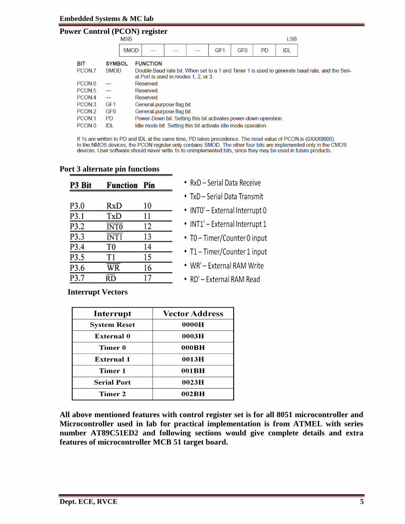
Power Control (PCON) register
Port 3 alternate pin functions
Interrupt Vectors
All above mentioned features with control register set is for all 8051 microcontroller and
Microcontroller used in lab for practical implementation is from ATMEL with series
number AT89C51ED2 and following sections would give complete details and extra
features of microcontroller MCB 51 target board.

Embedded Systems & MC lab
Dept. ECE, RVCE 6
INTRODUCTION TO ESA MCB 51 TARGET BOARD
This is a development board and supports a wide variety of 8051(with on-chip ROM)
compatible 8-bit microcontroller. ESA MCB 51 is designed to be general purpose development
board for single chip MCU applications that may be used as an instructional learning aid and
also as a development tool in R&D labs in industries. ESA MCB 51 development board is
built around Atmel AT89C51ED2/RD2 microcontroller.
ESA MCB 51 Capabilities
The powerful full-chip monitor provides communication with Keil µ Vision Debugger.
Executes user programs at full speed or debug the program using single step and break
point facilities available in Keil µ Vision debugger.
Examine/ modify the contents of CPU registers and memory contents.
On board LCD (16 x 2), interfaced to port lines.
All the 32 I/O lines are terminated on 4 different 10 pin connectors.
24 port lines (i.e. P0, P1 and P2) are terminated 0n 26-pin connector.
On board ISP (In-System Programming) support for on-chip flash programming.
Block Diagram: Fig 1
AT89C51ED2/RD2 Microcontroller
AT89C51RD2/ED2 is high performance CMOS Flash version of the 80C51 CMOS
single chip 8-bit microcontroller. It contains a 64-Kbyte Flash memory block for code. The 64-
Kbytes Flash memory can be programmed either in parallel mode or in serial mode with the
ISP(In System Programming) capability or with software. The programming voltage is
internally generated from the standard VCC pin.
The AT89C51RD2/ED2 retains all of the features of the Atmel 80C52 with 256 bytes of
internal RAM, a 9-source 4-level interrupt controller and three timer/counters. The
AT89C51ED2 provides 2048 bytes of EEPROM for non volatile data storage.
80C52 Architecture Compatible
– 8051 Instruction Compatible
– Four 8-bit I/O Ports (44 Pins Version)

Embedded Systems & MC lab
Dept. ECE, RVCE 7
– Three 16-bit Timer/Counters
– 256 Bytes Scratch Pad RAM
– 9 Interrupt Sources with 4 Priority Levels
ISP (In-System Programming) Using Standard VCC Power Supply
2048 Bytes Boot ROM Contains Low Level Flash Programming Routines and a default
Serial Loader
64K Bytes On-chip Flash Program/Data Memory
– Byte and Page (128 Bytes) Erase and Write
– 100k Write Cycles
On-chip 1792 bytes Expanded RAM (XRAM)
On-chip 2048 Bytes EEPROM Block for Data Storage (AT89C51ED2 Only)
SPI(Serial Peripheral ) Interface (Master/Slave Mode)
Full-duplex Enhanced UART with Dedicated Internal Baud Rate Generator
Hardware Watchdog Timer (One-time Enabled with Reset-Out)
Power Control Modes: Idle Mode, Power-down Mode
Block diagram of AT89C51ED2 Microcontroller: Fig 2
On-Chip memory of AT89C51ED2 Microcontroller: Fig 3
Embedded Systems & MC lab
Dept. ECE, RVCE 8
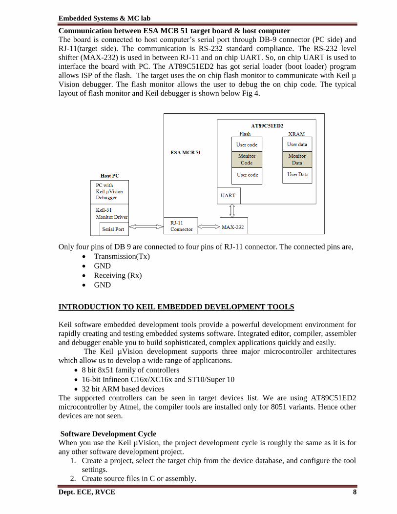
Communication between ESA MCB 51 target board & host computer
The board is connected to host computer’s serial port through DB-9 connector (PC side) and
RJ-11(target side). The communication is RS-232 standard compliance. The RS-232 level
shifter (MAX-232) is used in between RJ-11 and on chip UART. So, on chip UART is used to
interface the board with PC. The AT89C51ED2 has got serial loader (boot loader) program
allows ISP of the flash. The target uses the on chip flash monitor to communicate with Keil µ
Vision debugger. The flash monitor allows the user to debug the on chip code. The typical
layout of flash monitor and Keil debugger is shown below Fig 4.
Only four pins of DB 9 are connected to four pins of RJ-11 connector. The connected pins are,
Transmission(Tx)
GND
Receiving (Rx)
GND
INTRODUCTION TO KEIL EMBEDDED DEVELOPMENT TOOLS
Keil software embedded development tools provide a powerful development environment for
rapidly creating and testing embedded systems software. Integrated editor, compiler, assembler
and debugger enable you to build sophisticated, complex applications quickly and easily.
The Keil µVision development supports three major microcontroller architectures
which allow us to develop a wide range of applications.
8 bit 8x51 family of controllers
16-bit Infineon C16x/XC16x and ST10/Super 10
32 bit ARM based devices
The supported controllers can be seen in target devices list. We are using AT89C51ED2
microcontroller by Atmel, the compiler tools are installed only for 8051 variants. Hence other
devices are not seen.
Software Development Cycle
When you use the Keil µVision, the project development cycle is roughly the same as it is for
any other software development project.
1. Create a project, select the target chip from the device database, and configure the tool
settings.
2. Create source files in C or assembly.
Embedded Systems & MC lab
Dept. ECE, RVCE 9
3. Build your application with the project manager.
4. Correct errors in source files.
5. Test the linked application.
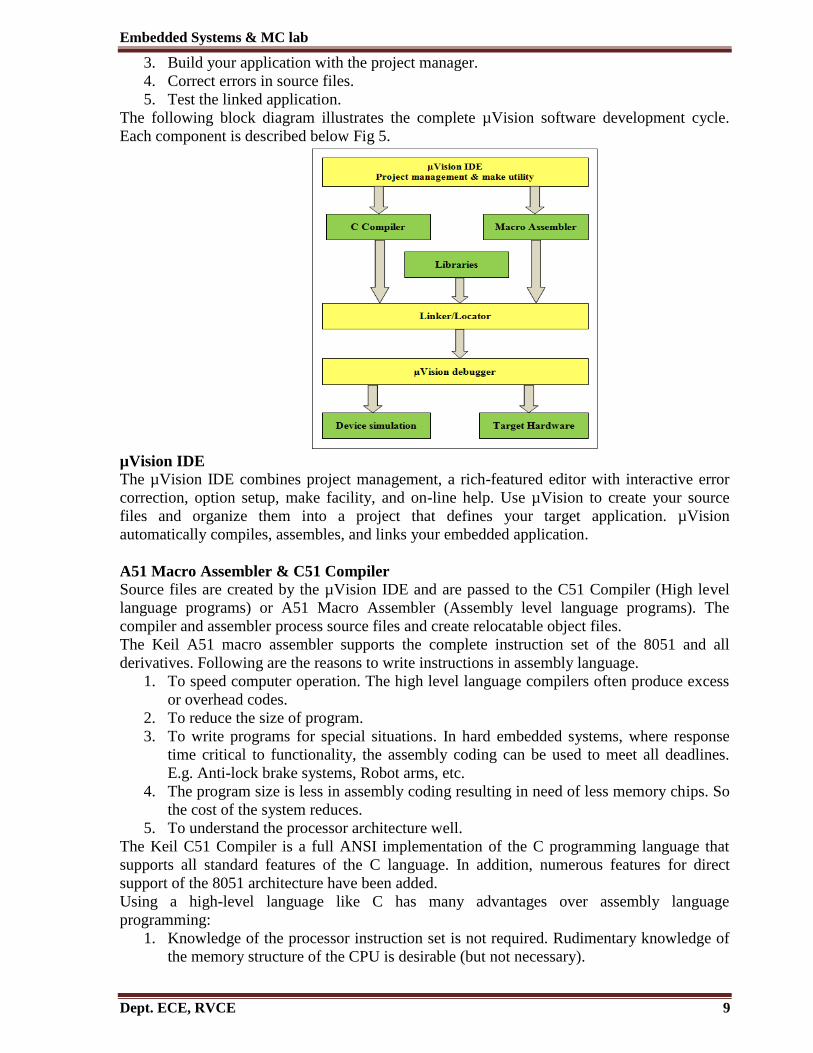
The following block diagram illustrates the complete µVision software development cycle.
Each component is described below Fig 5.
µVision IDE
The µVision IDE combines project management, a rich-featured editor with interactive error
correction, option setup, make facility, and on-line help. Use µVision to create your source
files and organize them into a project that defines your target application. µVision
automatically compiles, assembles, and links your embedded application.
A51 Macro Assembler & C51 Compiler
Source files are created by the µVision IDE and are passed to the C51 Compiler (High level
language programs) or A51 Macro Assembler (Assembly level language programs). The
compiler and assembler process source files and create relocatable object files.
The Keil A51 macro assembler supports the complete instruction set of the 8051 and all
derivatives. Following are the reasons to write instructions in assembly language.
1. To speed computer operation. The high level language compilers often produce excess
or overhead codes.
2. To reduce the size of program.
3. To write programs for special situations. In hard embedded systems, where response
time critical to functionality, the assembly coding can be used to meet all deadlines.
E.g. Anti-lock brake systems, Robot arms, etc.
4. The program size is less in assembly coding resulting in need of less memory chips. So
the cost of the system reduces.
5. To understand the processor architecture well.
The Keil C51 Compiler is a full ANSI implementation of the C programming language that
supports all standard features of the C language. In addition, numerous features for direct
support of the 8051 architecture have been added.
Using a high-level language like C has many advantages over assembly language
programming:
1. Knowledge of the processor instruction set is not required. Rudimentary knowledge of
the memory structure of the CPU is desirable (but not necessary).

Embedded Systems & MC lab
Dept. ECE, RVCE 10
2. Details like register allocation and addressing of the various memory types and data
types is managed by the compiler.
3. Programs get a formal structure (which is imposed by the C programming language)
and can be divided into separate functions. This contributes to
source code reusability as well as better overall application structure.
4. The ability to combine variable selection with specific operations improves program
readability.
5. Keywords and operational functions that more nearly resemble the human thought
process may be used.
6. Programming and program test time is drastically reduced.
7. The C run-time library contains many standard routines such as: formatted output,
numeric conversions, and floating-point arithmetic.
8. Existing program parts can be more easily included into new programs because of
modular program construction techniques.
9. The language C is a very portable language (based on the ANSI standard) that enjoys
wide popular support and is easily obtained for most systems. Existing program
investments can be quickly adapted to other processors as needed.
But compilers never generate optimized code as compared assembler which translates
assembly programs into machine codes. But, in some of the compilers special options will be
given to generate optimized code as in Keil software. Note that, while defining optimized code
memory requirement and execution time of object files are considered. The Keil software does
two types code optimization techniques (These can be enabled or disabled). In spite of all these
optimizations, object code generated by compilers is only comparable in speed and memory
requirement with that of object files generated by assemblers but not the same. Many
embedded development tools are now available with facility of writing assembly instructions
in high level language programs.
LIB51 Library Manager
The LIB51 library manager allows you to create object library from the object files created by
the compiler and assembler. Libraries are specially formatted, ordered program collections of
object modules that may be used by the linker at a later time. When the linker processes a
library, only those object modules in the library that are necessary to create the program are
used.
BL51 Linker/Locator
The BL51 Linker/Locator creates an absolute HEX file using the object modules extracted
from libraries and those created by the compiler and assembler. An absolute object file or
module contains no relocatable code or data. All code and data reside at fixed memory
locations. The absolute HEX file may be used:
To program an Flash ROM or other memory devices,
With the µVision Debugger for simulation and target debugging,
With an in-circuit emulator for the program testing.
µVision Debugger
The µVision symbolic, source-level debugger is ideally suited for fast, reliable program
debugging. The debugger includes a high-speed simulator that let you simulate an entire 8051
system including on-chip peripherals and external hardware. The attributes of the chip you use
are automatically configured when you select the device from the Device Database.
The µVision debugger offers two operating modes- Simulator mode and Target mode.
Simulator mode configures µVision debugger as software only product that accurately
simulates target systems including instructions and on-chip peripherals. This allows code

Embedded Systems & MC lab
Dept. ECE, RVCE 11
testing before hardware is available and gives you benefits for rapid, reliable embedded
software development.
Simulation allows software testing on your desktop with no hardware environment.
Early software debugging on a functional basis improves overall software reliability.
Simulation allows breakpoints that are impossible with hardware debuggers.
Simulation offers optimal input signal.
Failure scenarios that would destroy real hardware peripherals are easily checked.
The target mode connects the µvision debugger to real hardware. The appropriate target
driver is required depending on the target board connected. For ESA MCB-51 target board,
Keil Monitor-51 driver is used.
Intel HEX file
This is a file format for conveying binary information for applications like programming
microcontrollers, EPROMs, and other kinds of chips. The format is a text file, with each line
containing hexadecimal values encoding a sequence of data and their starting offset or absolute
address. There are three types of Intel HEX: 8-bit, 16-bit, and 32-bit. They are distinguished by
their byte order.
Each line of Intel HEX fioile consists of six parts:
1. Start code, one character, an ASCII colon ':'.
2. Byte count, two hex digits, a number of bytes (hex digit pairs) in the data field. 16
(0x10) or 32 (0x20) bytes of data are the usual compromise values between line length
and address overhead.
3. Address, four hex digits, a 16-bit address of the beginning of the memory position for
the data. Limited to 64 kilobytes, the limit is worked around by specifying higher bits
via additional record types. This address is big endian.
4. Record type, two hex digits, 00 to 05, defining the type of the data field.
5. Data, a sequence of n bytes of the data themselves. 2n hex digits.
6. Checksum, two hex digits - the least significant byte of the two's complement sum of
the values of all fields except fields 1 and 6 (Start code ":" byte and two hex digits of
the Checksum). It is calculated by adding together the hex-encoded bytes (hex digit
pairs), then leaving only the LSB of the result, and making a 2's complement (either by
subtracting the byte from 0x100, or inverting it by XOR-ing with 0xFF and adding
0x01).
For example, on : 0300300002337A1E
03 + 00 + 30 + 00 + 02 + 33 + 7A = E2, 2's complement is 1E
There are six record types:
00, data record, contains data and 16-bit address. The format described above.
01, End Of File record, a file termination record. No data. Has to be the last line of the
file, only one per file is permitted. Usually ':00000001FF'.
02, Extended Segment Address Record, segment-base address. Used when 16 bits are
not enough, identical to 80x86 real mode addressing. The address specified by the 02
record is multiplied by 16 (shifted 4 bits left) and added to the subsequent 00 record
addresses. This allows addressing of up to a megabyte of address space. The address
field of this record has to be 0000, the byte count is 02 (the segment is 16-bit). The least
significant hex digit of the segment address is always 0.
03, Start Segment Address Record. For 80x86 processors, it specifies the initial content
of the CS: IP registers. The address field is 0000, the byte count is 04, the first two
bytes are the CS value, the latter two are the IP value.

Embedded Systems & MC lab
Dept. ECE, RVCE 12
04, Extended Linear Address Record, allowing for fully 32 bit addressing. The address
field is 0000, the byte count is 02. The two data bytes represent the upper 16 bits of the
32 bit address, when combined with the address of the 00 type record.
05, Start Linear Address Record. The address field is 0000, the byte count is 04. The 4
data bytes represent the 32-bit value loaded into the EIP register of the 80386 and
higher CPU.

Embedded Systems & MC lab
Dept. ECE, RVCE 13
Experiment 1
a) Write an assembly language program to exchange 5 bytes of data at locations
0100H and at locations 0150H.
Algorithm
1. Initialize a source pointer (R0), a destination pointer (R1) & a counter (R3).
2. Get data from a source location into accumulator and save in a register
3. Get data from the destination location into accumulator.
4. Exchange the data at the two memory locations.
5. Update pointers to point to next elements in the arrays.
6. Decrement the count register and repeat from step 2 to 5 till count is zero.
Before Execution:
After Execution:
Program:
ORG 0000H
SJMP 30H
ORG 30H
MOV DPTR, #0100H
MOV R0, #00H ;source address
MOV R1, #50H ;destination address
MOV R3, #05H ;Block is of length 5 elements
BACK: MOV DPL, R0
MOVX A, @DPTR
MOV R2, A ; Save in a reg
MOV DPL, R1
MOVX A,@DPTR
XCH A, R2
MOVX @DPTR, A
MOV DPL, R0
Embedded Systems & MC lab
Dept. ECE, RVCE 14
MOV A, R2
MOVX @DPTR, A
INC R0
INC R1
DJNZ R3, BACK
HERE: SJMP HERE
END
Output:
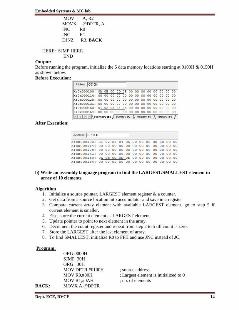
Before running the program, initialize the 5 data memory locations starting at 0100H & 0150H
as shown below.
Before Execution:
After Execution:
b) Write an assembly language program to find the LARGEST/SMALLEST element in
array of 10 elements.
Algorithm
1. Initialize a source pointer, LARGEST element register & a counter.
2. Get data from a source location into accumulator and save in a register
3. Compare current array element with available LARGEST element, go to step 5 if
current element is smaller.
4. Else, store the current element as LARGEST element.
5. Update pointer to point to next element in the array.
6. Decrement the count register and repeat from step 2 to 5 till count is zero.
7. Store the LARGEST after the last element of array.
8. To find SMALLEST, initialize R0 to FFH and use JNC instead of JC.
Program:
ORG 0000H
SJMP 30H
ORG 30H
MOV DPTR,#0100H ; source address
MOV R0,#00H ; Largest element is initialized to 0
MOV R1,#0AH ; no. of elements
BACK: MOVX A,@DPTR

Embedded Systems & MC lab
Dept. ECE, RVCE 15
MOV R2,A
CLR C
SUBB A,R0 ; if A> R0, carry flag is 0
JC LOOP
MOV A,R2
MOV R0,A
LOOP: INC DPTR
DJNZ R1,BACK
MOV A,R0 ; Store the largest element
MOVX @DPTR,A
HERE: SJMP HERE
End
Output: Before Execution:
After Execution: Underlined element is largest.
c) Write an assembly language program to sort an array of elements using BUBBLE
SORT. Array starts from location 0101H and size of the array is at location
0100H.
Algorithm
1. Initialize a source pointer, an ITERATION (outer-R3) counter & a COMPARISON
(inner-R2) counter.
2. Check the number of elements and if it is equal to 0 or 1, end program.
3. Compare the current and the next element in the array.
4. If the current element is larger (smaller for descending order) then exchange the 2
numbers in the array.
5. Decrement the COMPARISON counter and repeat through step 4 until this counter
becomes 0.
6. Decrement the ITERATION counter and repeat through step 3 until this counter
becomes zero.
7. For descending order use JC instead of JNC.
The given list
28 58 84 16 270 42 19 77 59 17 27 255
Embedded Systems & MC lab
Dept. ECE, RVCE 16
Iteration 1 28 58 16 84 42 19 77 59 17 27 57 255
Iteration 2 28 16 58 42 19 77 59 17 27 57 84 255
Iteration 3 16 28 42 19 58 59 17 27 57 77 84 255
Iteration 4 16 28 19 42 58 17 27 57 59 77 84 255
Iteration 5 16 19 28 42 17 27 57 58 59 77 84 255
Iteration 6 16 19 28 17 27 42 57 58 59 77 84 255
Iteration 7 16 19 17 27 28 42 57 58 59 77 84 255
Iteration 8 16 17 19 27 28 42 57 58 59 77 84 255
Iteration 9 16 17 19 27 28 42 57 58 59 77 84 255
Iteration10 16 17 19 27 28 42 57 58 59 77 84 255
Iteration 11 16 17 19 27 28 42 57 58 59 77 84 255
The final sorted list
16 17 19 27 28 42 57 58 59 77 84 255
Note that, 11 iterations are required to sort array of 12 elements .Totally, 11 comparisons
are to be done in first iteration and is reduces by 1 for each subsequent iteration.
Program:
ORG 0000H
SJMP 30H
ORG 30H
MOV DPTR, # 0100H ;Number of elements
MOVX A, @DPTR
JZ STOP ;compare with zero
MOV R3, A
CLR C
SUBB A, #01H
JZ STOP ;compare with 1
DEC R3
NEXT1: MOV A,R3
MOV R2,A
MOV DPTR, # 0101H ;First element
NEXT : MOVX A, @DPTR
MOV R0, A
INC DPTR
MOVX A, @DPTR ;second element
MOV R1, A
CLR C
SUBB A, R0 ;(2nd - 1st) no 2nd >1st no exchange
JNC NOEXCH ; JC for descending order
MOV A, R0 ; This code excahnge two elements
MOVX @DPTR , A
DEC DPL
MOV A, R1
MOVX @DPTR, A
INC DPTR
NOEXCH: DJNZ R2, NEXT
DJNZ R3, NEXT1
STOP: SJMP STOP

Embedded Systems & MC lab
Dept. ECE, RVCE 17
END
Output:
Before Execution: The encircled number in the figure is no. of elements.
After Execution:
d) Write an assembly language program to find the sum of an array of 8-bit BCD
numbers starting at location 0100H. Store the result at location 0150H (Most
Significant Byte) & 0151H (Least Significant Byte).
Algorithm
1. Initialize a source pointer, a counter & a 16-bit result (partial SUM) register.
2. Add the first element to partial SUM register & suitably consider carry generated.
3. Adjust the result suitably to decimal form.
4. Update pointer to point to next element in the array.
5. Decrement the count register and repeat from step 2 to 4 till count is zero.
6. Store the result present in partial SUM registers to the appropriate memory locations.
Program:
ORG 0000H
SJMP 30H
ORG 30H
MOV DPTR, #0100H ;Source Address
MOV R1, # 00H ;Partial Sum Lsbyte
MOV R2, # 00H ;Partial Sum Msbyte
MOV R3, # 05H ;Count
BACK: MOVX A,@DPTR
ADD A, R1
DA A ;Adjust Ls Part Of Result To Bcd Form
MOV R1, A
JNC NEXT
MOV A, R2 ;Adjust Ms Part Of Result Also
ADD A, #01H
DA A
MOV R2,A
NEXT: INC DPTR

Embedded Systems & MC lab
Dept. ECE, RVCE 18
DJNZ R3, BACK
MOV DPTR,#0150H
MOV A, R2
MOVX @DPTR, A ;Store The Result
INC DPTR
MOV A, R1
MOVX @DPTR, A
HERE: SJMP HERE
END
Output:
Before Execution: Enter BCD input
After Execution:
Observations to be recorded for Experiment 1
1. Use of ORG 0000H & END statements
2. Use of SJMP 30H & ORG 30H statements
3. Use of HERE:SJMP HERE statement
4. HEX file of any one program
5. Use of MOVX statement
6. Use of DA A instruction

Embedded Systems & MC lab
Dept. ECE, RVCE 19
7. .lst file of any one program
8. Setting clock a real number
9. Use of AT89c51ED2 as a target
10. Contents of code memory as seen in memory window of Keil for any one program
Embedded Systems & MC lab
Dept. ECE, RVCE 20
Experiment 2
a) Write an assembly language program to find the product of a 16-bit number & an 8-
bit number stored at location 0100h, 0101h & 0102h. Store the result at locations
0103h, 0104h & 0105h.
Algorithm
1. Initialize a set of registers with operands.
2. Multiply the LS byte of the multiplicand with the multiplier.
3. Store the LS part of result & preserve the MS part of the result in a register.
4. Multiply the MS byte of the multiplicand with the multiplier.
5. Add the LS part of present result with MS part of the previous result & store it.
6. Add the MS part of present result with carry of the previous addition & store it
Program:
ORG 0000H
SJMP 30H
ORG 30H
MOV DPTR,#0101H
MOVX A,@DPTR
MOV B,A ;LS Byte Of Multiplier (LS)
MOV DPTR,#0100H
MOVX A,@DPTR
MOV R1,A ; MS byte of Multiplier (MS)
MOV DPTR,#0102H
MOVX A, @DPTR
MOV R2,A ; 8-bit multiplicand (MUP)
MUL AB ; LS x MUP= 16 bit partial result1
INC DPTR ; A-LS byte, B-MS byte
MOVX @DPTR, A ;save LS byte of result1 in 0103H
MOV A,R2
MOV R3,B
MOV B,R1
MUL AB ;MS x MUP= 16 partial result2
ADD A,R3 ; MS byte of partial result1+ LS byte of partial
INC DPTR ; result2
MOVX @DPTR,A ;Save second byte of result in 0104H
CLR A
ADDC A,B ;add carry of previous addtion to MS byte of
INC DPTR ; partial result2
MOVX @DPTR,A ;Save MS byte of result in 0105H
HERE: SJMP HERE
END
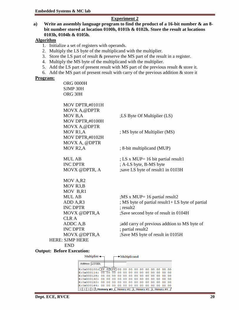
Output: Before Execution:

Embedded Systems & MC lab
Dept. ECE, RVCE 21
After Execution:The correct result in odrder is FEFF01H
b) Write an assembly language program to divide a 16-bit number in R2 & R3 by
another 8-bit number in R4. Store the result at location 150h & 151h.
Algorithm
1. The division operation is implemented as repeated subtraction.
2. Initialize a set of registers with operands & a 16 bit quotient register.
3. Convert the 8 bit divisor to a 16 bit number (by prefixing 0’s).
4. Subtract the 16 bit divisor from the 16 bit dividend & increment the quotient register.
5. Repeat step 3 as long as (dividend) > (divisor).
6. Store the result i.e. quotient & remainder at suitable locations.
Program:
ORG 0000H
SJMP 30H
ORG 0030H
MOV R2,#0FFh ;MS byte of 16 bit dividend
MOV R3, #0FFh ;LS byte of 16 bit dividend
MOV R4, #0E8H ; 8-bit divisor
MOV R5,#00H ; The operation is (R2R3) / (R5R4)
MOV DPTR,#0FFFFH ;16 bit quotient in DPTR
BACK: INC DPTR
MOV A, R2
CLR C
SUBB A, R4 ; Subtract divisor from MS byte
MOV R2, A
MOV A, R3
SUBB A, R5 ; Subtract divisor from LS byte
MOV R3, A
JNC BACK ; Repeat until (Dividend >Divisor)
MOV A, R2 ; Get the correct remainder
ADD A, R4
MOV R2, A
MOV A, R3
ADDC A, R5
MOV R3, A
MOV A, DPH ; This code store result
MOV R0, DPL ; Quotient will be there in DPTR (16-bit)
MOV DPTR, #0150H

Embedded Systems & MC lab
Dept. ECE, RVCE 22
MOVX @DPTR, A
MOV A, R0
INC DPTR ; The 16-bit remainder will be there in
MOVX @DPTR, A ; R3(MS byte) and R2(LS byte)
MOV A, R3
INC DPTR
MOVX @DPTR, A
MOV A, R2
INC DPTR
MOVX @DPTR, A
OVER: SJMP OVER
END
Output: After Execution:
The above program also performs division of two sixteen bit numbers. Change the values of
registers depending upon operation required.
c) i) Write an ALP to implement (display) an eight bit up/down binary (hex) counters
on watch window.
Algorithm:
1. Initialize A - register with 00h
2. Use a delay subroutine (in delay program load designed values to R1, R2 and R3, loop
and decrement until 0) to create a delay of 1 second.
3. Increment A - register (decrement for down counter) repeatedly.
Program:
ORG 0000H
SJMP 30H
ORG 30H
MOV A,#00
BACK: ACALL DELAY
INC A ; decrement a for binary down counter
SJMP BACK
DELAY: MOV R1,#20H
DECR: MOV R2,#0FFH
DECR1: MOV R3,#0FFH
HERE: DJNZ R3,HERE
DJNZ R2,DECR1
DJNZ R1, DECR
RET
END
Note: To run this program, after selecting DEBUG session in the main menu, select
Embedded Systems & MC lab
Dept. ECE, RVCE 23
View-> Watch& call Stack window, in the Watches select watch 1(or 2) and press F2
and enter a (for accumulator A) as shown below.
ii) Write an ALP to implement (display) an eight bit up/down BCD counters on
watch window.
Algorithm:
1. Initialize A - register with 00h
2. Use a delay subroutine (in delay program load designed values to registers R1, R2 and
R3, loop and decrement until 0) to create a delay of 1 second.
3. Add A register with 01 and decimal adjust the result (for down counter add 99h)
repeatedly.
Program:
ORG 0H
SJMP 30H
ORG 30H
MOV A,#00
BACK:ACALL DELAY
ADD A,#99H ;ADD, #01 for BCD up counter
DA A
JNZ BACK
HERE:SJMP HERE
DELAY: MOV R1,#20H
DECR1: MOV R2,#0FFH
DECR: MOV R3, #0FFH
TEMP: DJNZ R3,TEMP
DJNZ R2, DECR
DJNZ R1, DECR1
RET
END
Note: To run this program, after selecting DEBUG session in the main menu, select
View-> Watch& call Stack window, in the Watches select watch 1(or 2) and press F2
and enter a (for accumulator A)
d) Write an ALP using subroutines to perform the following; an array of 4 elements is
stored in external memory locations starting from 0100H;
i) If the first two elements are equal, then store ‘1’ in the first bit (00H) of bit
addressable memory, else, store ‘0’.
ii) If the last two elements are equal, then store ‘1’ in the last bit of bit addressable
memory (7FH), else, store ‘0’.
iii) If both these bits are set, then logically AND all 4 elements; else logically OR
them and store the result in 5th
location of the array.
Embedded Systems & MC lab
Dept. ECE, RVCE 24
Algorithm:
1. Read the elements of the array from the address 0100h
2. Compare the first 2 numbers for equality using sub-routine FIRST & store result in bit
address 00h.
3. Compare the last 2 numbers for equality using sub-routine SECOND & store result in
bit address 7Fh.
4. Check the result of steps 2 & 3; if both bits are set, then logically AND all elements
using L_AND sub-routine; else, logically OR them using L_OR sub-routine.
5. Store the result in 5th
location.
Program:
ORG 0000H
SJMP 30H
ORG 30H
MOV DPTR,#0100H
MOVX A,@DPTR
MOV R0,A
INC DPTR
MOVX A,@DPTR
MOV R1, A
ACALL FIRST
INC DPTR
MOVX A,@DPTR
MOV R2,A
INC DPTR
MOVX A,@DPTR
MOV R3,A
ACALL SECOND
JNB 7FH, NEXT
JNB 00H, NEXT
ACALL L_AND
OVER:INC DPTR
MOVX @DPTR, A
STOP: SJMP STOP
NEXT: ACALL L_OR
JMP OVER
FIRST: CJNE A,00H, SKIP
SETB 00H
RET
SKIP: CLR 00H
RET
SECOND: CJNE A,02H, SKIP1
SETB 7FH
RET
SKIP1: CLR 7FH
RET
Embedded Systems & MC lab
Dept. ECE, RVCE 25
L_AND: MOV A, R0
ANL A,R1
ANL A,R2
ANL A,R3
RET
L_OR: MOV A, R0
ORL A,R1
ORL A,R2
ORL A,R3
RET
END
Output: Before Execution:
After Execution:
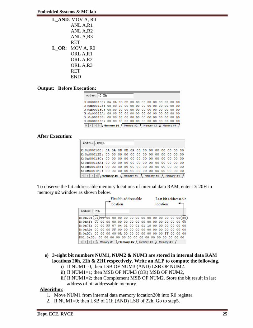
To observe the bit addressable memory locations of internal data RAM, enter D: 20H in
memory #2 window as shown below.
e) 3-eight bit numbers NUM1, NUM2 & NUM3 are stored in internal data RAM
locations 20h, 21h & 22H respectively. Write an ALP to compute the following.
i) If NUM1=0; then LSB OF NUM3 (AND) LSB OF NUM2.
ii) If NUM1=1; then MSB OF NUM3 (OR) MSB OF NUM2,
iii) If NUM1=2; then Complement MSB OF NUM2. Store the bit result in last
address of bit addressable memory.
Algorithm:
1. Move NUM1 from internal data memory location20h into R0 register.
2. If NUM1=0; then LSB of 21h (AND) LSB of 22h. Go to step5.

Embedded Systems & MC lab
Dept. ECE, RVCE 26
3. If NUM1=1; then MSB of 21h (OR) MSB of 22h. Go to step5.
4. If NUM1=2; then complement MSB of 21h. Go to step5
5. Store the result at MSB bit of 7Fh location.
Program: ORG 00H
SJMP 30h
ORG 30h
MOV R0,20H ;R0 - NUM1
CJNE R0,#0,CK1
MOV C,08H ;LSB of NUM2 (21H) - bit address -08h
ANL C,10H ;LSB of NUM3 (22H) - bit address -10h
SJMP LAST
CK1:CJNE R0,#1,CK2
MOV C,0FH ;MSB of NUM2 (21H) - bit address -0Fh
ORL C,17H ;MSB of NUM3 (22H) - bit address -17h
SJMP LAST
CK2:CJNE R0,#2,CK3
CPL 0FH
MOV C,0FH ;MSB of NUM1 (21H) - bit address -0Fh
SJMP LAST
CK3:CLR C
LAST:MOV 7Fh,C ;RES location -7Fh
HERE:SJMP HERE
END
Output:
Run 1:
Before Execution:
RAM location: 20h=00h (NUM1)
RAM location: 21h=FFh(NUM2)
RAM location: 22h=FFh(NUM3)
After Execution:
RAM location: 20h=00h(NUM1)
RAM location: 21h=FFh(NUM2)
RAM location: 22h=FFh(NUM3)
RAM location: 2Fh=80h (NUM2LSB AND NUM3LSB)
Run 2:
Before Execution:
RAM location: 20h=01h (NUM1)
RAM location: 21h=FFh(NUM2)
RAM location: 22h=FFh(NUM3)
After Execution:
RAM location: 20h=01h(NUM1)
RAM location: 21h=FFh(NUM2)
RAM location: 22h=FFh(NUM3)
RAM location: 2Fh=80h (NUM2MSB OR NUM3MSB)
Run 3:
Before Execution:
Embedded Systems & MC lab
Dept. ECE, RVCE 27
RAM location: 20h=02h (NUM1)
RAM location: 21h=FFh(NUM2)
RAM location: 22h=FFh(NUM3)
After Execution:
RAM location: 20h=02h(NUM1)
RAM location: 21h=7Fh(NUM2 MSB is complemented)
RAM location: 22h=FFh(NUM3)
RAM location: 2Fh=00h (NOT of NUM2MSB)
The bit address 7Fh is MSB of RAM location 2Fh.
Observations to be recorded for Experiment 2
1. Pointer for program memory & data memory.
2. Effect of changing clock frequency on program execution time, delay loops
3. Use call stack window
4. Use of Byte level & Bit level instructions
5. Opcode for all ACALL instructions in a program
6. Contents of data memory as seen in Keil memory window
7. Use of ASCII symbols
8. Use of peripheral window of to observe timer count sequence
9. Effect of clock frequency on timer delay
10. Instruction execution time in terms of clock cycles, machine cycles & instruction cycle

Embedded Systems & MC lab
Dept. ECE, RVCE 28
Experiment 3
a) Write an ALP to convert a BCD number stored at a location into its ASCII
equivalent number.
Algorithm 1. Move the BCD data to be converted to accumulator.
2. Get the lower nibble(BCD digit) & ADD (or ORL) with 30h
3. Store the converted ASCII value
4. Get the higher nibble(tens BCD digit) & ADD (or ORL) with 30h
5. Store the converted ASCII value
Program:
ORG 0000H
SJMP 30h
ORG 30h
MOV R1,#50H
MOV A,@R1 ;get BCD data byte from RAM location 50h
MOV R2,A ;Store in R2
ANL A,#0FH ;Get the lower nibble
ORL A,#30H ;Add/OR with 30h i.e., 0-9 converted to 30-39h
INC R1
MOV @R1,A ;Store the lower digit's ASCII code
MOV A,R2 ;Get back the number
SWAP A ;Swap nibbles in A
ANL A,#0FH ;Get the upper BCD digit
ORL A,#30H ;Convert to ASCII
INC R1
MOV @R1,A ;Store the upper digit's ASCII code
HERE: SJMP HERE
END
Output:
Before Execution:
Internal RAM location: 50H=28(BCD)
Internal RAM location: 51H=00
Internal RAM location: 52H=00
After Execution:
Internal RAM location: 50H=28(BCD)
Internal RAM location: 51H=38(ASCII equivalent of 8)
Internal RAM location: 52H=32(ASCII equivalent of 2)
b) Write an ALP to generate a square wave of 2 KHz, duty cycle 0.5 on P1.5 by
programming on-chip timer in mode-1.
Algorithm:
1. Initialize Timer0 in mode-1.
2. Load suitable values in to TH0 and TL0 registers.
3. Set P1.5 pin for 250 µSec and clear for another 250µSec.
4. Repeat step 2 and 3 indefinitely.
The given data is,
Period=500 µSec Duty cycle=50% TON=250µSec TOFF= 250µSec
Input clock frequency to Timer0= Oscillator frequency/12=11.0592/12=0.9216 MHz
Let the number states of TL0 register required for 250 µSec be x.
Embedded Systems & MC lab
Dept. ECE, RVCE 29
250 µSec=x(1/0.9216 M)=>x=230.4
Therefore, the value to be loaded into TL0 register=256-230=26D=1AH
For different duty cycles, load different values into TL0 register for TON & TOFF.
Program:
ORG 0h
SJMP 30h
ORG 30h
MOV TMOD, #01H ; Timer-0, mode-1
REP: MOV TL0, #1Ah ; TON period
MOV TH0, #0FFh
SETB P1.5
ACALL DEL
MOV TL0, #1Ah ;TOFF period
MOV TH0, #0FFh
CLR P1.5
ACALL DEL
SJMP REP
DEL: SETB TR0 ; this is delay routine
HERE: JNB TF0, HERE
CLR TR0
CLR TF0
RET
END
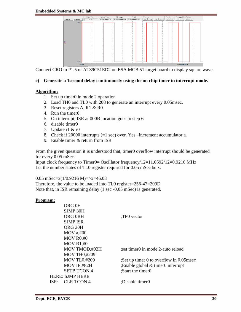
Output:
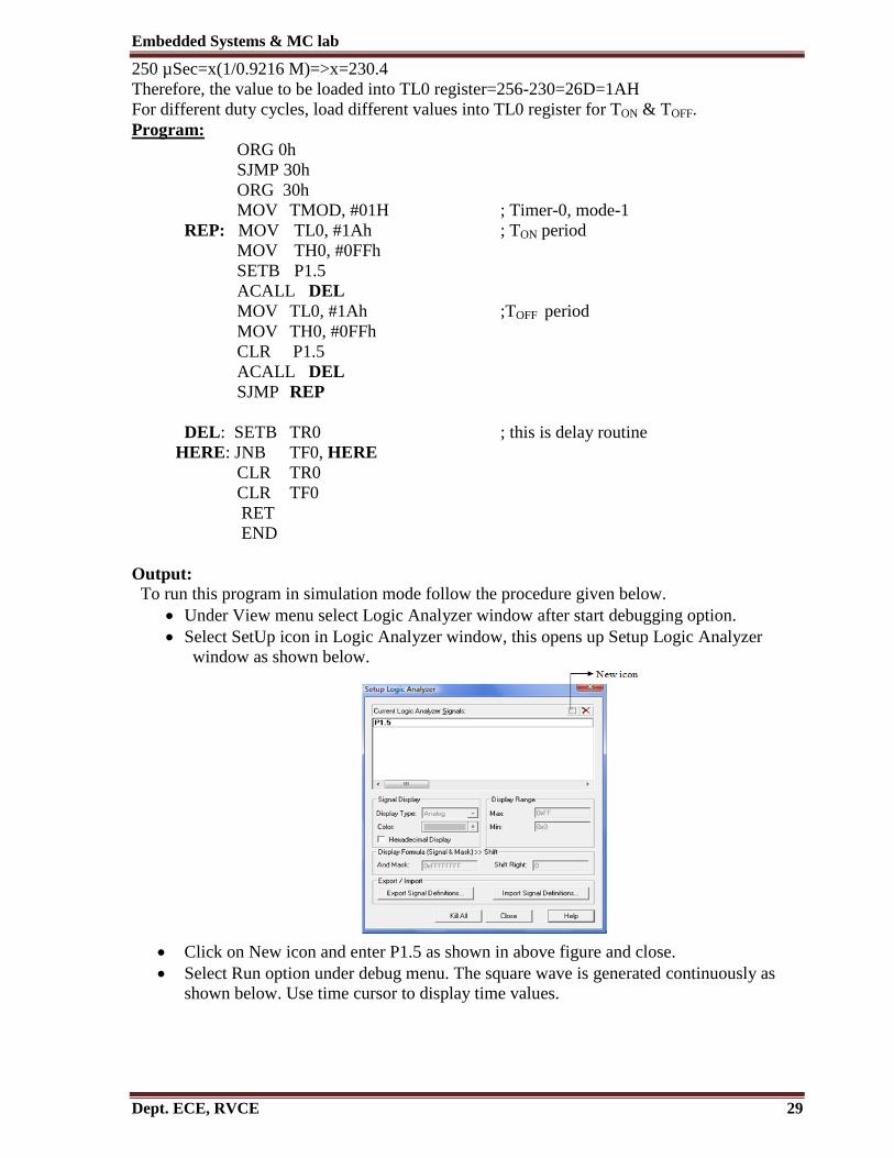
To run this program in simulation mode follow the procedure given below.
Under View menu select Logic Analyzer window after start debugging option.
Select SetUp icon in Logic Analyzer window, this opens up Setup Logic Analyzer
window as shown below.
Click on New icon and enter P1.5 as shown in above figure and close.
Select Run option under debug menu. The square wave is generated continuously as
shown below. Use time cursor to display time values.
Embedded Systems & MC lab
Dept. ECE, RVCE 30
Connect CRO to P1.5 of AT89C51ED2 on ESA MCB 51 target board to display square wave.
c) Generate a 1second delay continuously using the on chip timer in interrupt mode.
Algorithm:
1. Set up timer0 in mode 2 operation
2. Load TH0 and TL0 with 208 to generate an interrupt every 0.05msec.
3. Reset registers A, R1 & R0.
4. Run the timer0.
5. On interrupt; ISR at 000B location goes to step 6
6. disable timer0
7. Update r1 & r0
8. Check if 20000 interrupts (=1 sec) over. Yes –increment accumulator a.
9. Enable timer & return from ISR
From the given question it is understood that, timer0 overflow interrupt should be generated
for every 0.05 mSec.
Input clock frequency to Timer0= Oscillator frequency/12=11.0592/12=0.9216 MHz
Let the number states of TL0 register required for 0.05 mSec be x.
0.05 mSec=x(1/0.9216 M)=>x=46.08
Therefore, the value to be loaded into TL0 register=256-47=209D
Note that, in ISR remaining delay (1 sec -0.05 mSec) is generated.
Program:
ORG 0H
SJMP 30H
ORG 0BH ;TF0 vector
SJMP ISR
ORG 30H
MOV a,#00
MOV R0,#0
MOV R1,#0
MOV TMOD,#02H ;set timer0 in mode 2-auto reload
MOV TH0,#209
MOV TL0,#209 ;Set up timer 0 to overflow in 0.05msec
MOV IE,#82H ;Enable global & timer0 interrupt
SETB TCON.4 ;Start the timer0
HERE: SJMP HERE
ISR: CLR TCON.4 ;Disable timer0

Embedded Systems & MC lab
Dept. ECE, RVCE 31
INC r1 ;r1*r2 = 100*200 = 20000 * 0.05msec = 1sec
CJNE r1,#100,SKIP
MOV r1,#00
INC r0
CJNE r0,#200,SKIP
MOV r0,#00H
INC A
SKIP: SETB TCON.4 ; Enable Timer
RETI ; Return from interrupt subroutine
END
Output:
Observe the value of accumulator incrementing approximately for every 1 sec in watch and
call stack window.
Observations to be recorded for Experiment 3
1. Advantage of generating delay using Timers
2. Methods to generate delay
3. Use of call stack window
4. Values of TH0, TL0 for generating 4KHz frequency with 75% duty cycle
5.

Embedded Systems & MC lab
Dept. ECE, RVCE 32
Experiment 4
a) Write an 8051 C program to interface Logic Controller card and perform various
logical functions.
Logic Controller Interface:
Logic controller interface consists of 8 TTL inputs connected to 8 DIP switches & 8 TTL
outputs connected to 8 LEDs. Another set of 8 LEDs used to indicate status of each DIP
switch. Using this interface card, different logical operations can be performed. To give
input, DIP switches can be used and to output can be displayed on LEDs. [Input port is P1
and the Output port is P0 for interfacing board, switch 2 (SW2) on board for updating
input changes].
Connection diagram:
From the connection diagram, it is observed that the DIP switches are connected to port
1(to be configured as input) output LEDs are connected to port 0(to be configured as
output). So, the control word for above configurations is obtained as follows. (Port 2 is not
used)
Program:
#include<reg51.h>
void msdelay(unsigned int itime)
unsigned int i,j;
for(i=0;i<1275;i++)
for(j=0;j<itime;j++) ;
void main()
unsigned char arr[] = 0x00, 0x02, 0x02, 0x01, 0x02, 0x01, 0x01, 0x03, temp;
P0=0x00; // output port
P1 = 0xff; // configuration input port
while(1)
P0 = 0x03 & P0; // masking MSB bits for full adder operation
temp = P1 & 0x07;

Embedded Systems & MC lab
Dept. ECE, RVCE 33
if (temp ==0)
P0 = arr[0];
else if (temp ==1)
P0 = arr[1];
else if (temp ==2)
P0 = arr[2];
else if (temp ==3)
P0 = arr[3];
else if (temp ==4)
P0 = arr[4];
else if (temp ==5)
P0 = arr[5];
else if (temp ==6)
P0 = arr[6];
else
P0 = arr[7];
msdelay(50);
Activity: Do 4 possible logical operations using the above program (full subtracter,
logical OR, XOR etc.,)
b) Write 8051 C program to interface stepper motor to rotate in clockwise/ anti
clockwise directions & and to rotate the motor through predefined angle of rotation.
The stepper motor is a widely used device that translates electrical pulses into
mechanical movement. In applications such as disk drives, dot matrix printers, and robotics,
the stepper motor is used for position control.
Stepper motors commonly have a central magnet called rotor or shaft surrounded
by stator. The most common stepper motors have four stator windings that are paired with
center-tapped common as shown in figure below. This type of stepper motor is commonly
called as a four-phase or unipolar stepper motor. Hence, the unipolar stepper motors have 6
leads: 4 representing the four stator windings and 2 commons for the center tapped leads.
The stepper motor moves in fixed repeatable increment, which allows one to move it
to a fixed precise position. The direction of rotation is dictated by the stator poles. The stator
poles are determined by the current sent through the wire coils. As direction of current
changed, the polarity is also changed causing motor rotate in opposite direction. As the

Embedded Systems & MC lab
Dept. ECE, RVCE 34
sequence of power is applied to each stator winding, the rotor will rotate. There are several
widely used sequences where each has a different degree of precision. The table below shows
1-phase, 4-step stepping sequence. It is 1-phase because at any time only one coil is excited. It
must be noted that although we can start with any of the sequences in table, once we start we
must continue in the proper order.
Step coil A coil B coil C coil D
1 0 0 0 1
2 1 0 0 0
3 0 1 0 0
4 0 0 1 0
Anyone of these values forms the initial value. The step angle is minimum degree of
rotation associated with a single step. This depends on number teeth on rotor and stator. The
step angle of motor using in lab is 1.8º. So, the steps per revolution is 200 (360o
/ 1.8o). Note
that, after completing every four steps, the rotor moves only by one tooth pitch. Therefore, in a
stepper motor with 200 steps per revolution, the rotor has 50 teeth since 4 x 50=200 steps are
needed to complete one revolution (Refer figure below). The curtain amount of minimum of
current is required to energize the coils. Since, 8051 lacks sufficient current to drive, a driver
(Darlington pair formed by 2N3055 & SL100) is used. It must be noted that P0.0 is connected
to coil C, P0.1 is connected to coil D, P0.2 is connected to coil A, P0.3 is connected to coil B.
Interfacing diagram:
Anti clockwise Clockwise
Embedded Systems & MC lab
Dept. ECE, RVCE 35
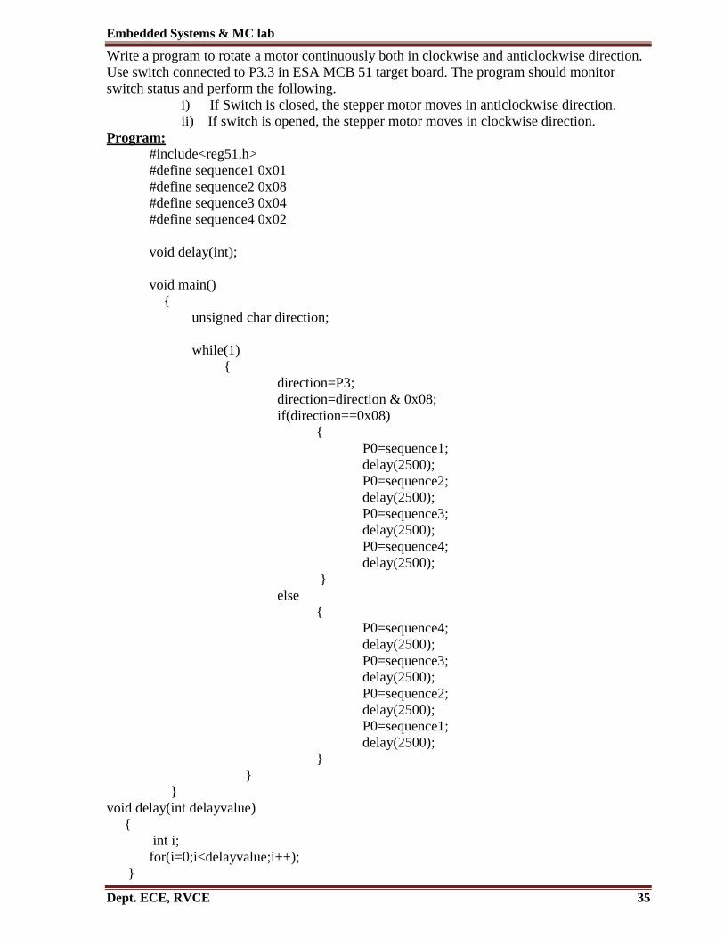
Write a program to rotate a motor continuously both in clockwise and anticlockwise direction.
Use switch connected to P3.3 in ESA MCB 51 target board. The program should monitor
switch status and perform the following.
i) If Switch is closed, the stepper motor moves in anticlockwise direction.
ii) If switch is opened, the stepper motor moves in clockwise direction.
Program:
#include<reg51.h>
#define sequence1 0x01
#define sequence2 0x08
#define sequence3 0x04
#define sequence4 0x02
void delay(int);
void main()
unsigned char direction;
while(1)
direction=P3;
direction=direction & 0x08;
if(direction==0x08)
P0=sequence1;
delay(2500);
P0=sequence2;
delay(2500);
P0=sequence3;
delay(2500);
P0=sequence4;
delay(2500);
else
P0=sequence4;
delay(2500);
P0=sequence3;
delay(2500);
P0=sequence2;
delay(2500);
P0=sequence1;
delay(2500);
void delay(int delayvalue)
int i;
for(i=0;i<delayvalue;i++);
Embedded Systems & MC lab
Dept. ECE, RVCE 36
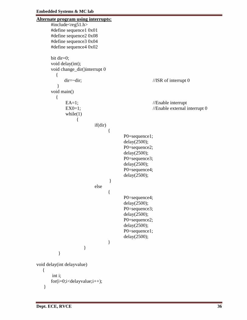
Alternate program using interrupts:
#include<reg51.h>
#define sequence1 0x01
#define sequence2 0x08
#define sequence3 0x04
#define sequence4 0x02
bit dir=0;
void delay(int);
void change_dir()interrupt 0
dir=~dir; //ISR of interrupt 0
void main()
EA=1; //Enable interrupt
EX0=1; //Enable external interrupt 0
while(1)
if(dir)
P0=sequence1;
delay(2500);
P0=sequence2;
delay(2500);
P0=sequence3;
delay(2500);
P0=sequence4;
delay(2500);
else
P0=sequence4;
delay(2500);
P0=sequence3;
delay(2500);
P0=sequence2;
delay(2500);
P0=sequence1;
delay(2500);
void delay(int delayvalue)
int i;
for(i=0;i<delayvalue;i++);

Embedded Systems & MC lab
Dept. ECE, RVCE 37
Write a program to rotate motor 180º in the clockwise direction. The motor step angle is 1.8º.
Use the 4-step sequence.
The given data is,
Step angle=1.8º /step
Therefore, for 4-step the angle of rotation= 4x1.8 =7.2º.
For 180º, the 4-step sequence must be repeated for 25 times(180º / 7.2º)
Program:
#include <REG51.H>
void delay (unsigned int x)
for(;x>0;x--);
return;
main ( )
unsigned char val;
int x=0,i;
P0=0x00;
while(x<25)
val=0x11;
for(i=0;i<4;i++)
P0=val;
val=val>>1; //Perform << shift for other direction.
delay(5000);
x++;
for(;;);
Alternate exam questions:
1. Write a program to rotate stepper motor 45 degrees in clockwise & 90 degrees in anti
clockwise direction continuously.
2. Write a program to rotate stepper motor continuously in clockwise direction for 1 sec,
halt for 0.5 sec and in anticlockwise direction for 1sec, halt for 2 sec and repeat.
Observations to be recorded for Experiment 4
1. Use of micro stepping in stepper motor
2. Writing program in assembly and ‘C’[code size and program execution]
3. Memory location for Variables declared in ‘C’

Embedded Systems & MC lab
Dept. ECE, RVCE 38
4. Use of REG51.h header file
5. Purpose of using interrupts over polling mode
6. Contents of stack for function calls in C program
7. Use of flash as program memory
8. Logic high and logic low voltage levels of port pins
9. Stepper motor voltage & current ratings
Embedded Systems & MC lab
Dept. ECE, RVCE 39
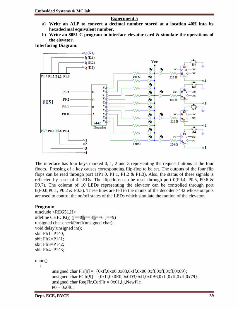
Experiment 5
a) Write an ALP to convert a decimal number stored at a location 40H into its
hexadecimal equivalent number.
b) Write an 8051 C program to interface elevator card & simulate the operations of
the elevator.
Interfacing Diagram:
The interface has four keys marked 0, 1, 2 and 3 representing the request buttons at the four
floors. Pressing of a key causes corresponding flip-flop to be set. The outputs of the four flip
flops can be read through port 1(P1.0, P1.1, P1.2 & P1.3). Also, the status of these signals is
reflected by a set of 4 LEDs. The flip-flops can be reset through port 0(P0.4, P0.5, P0.6 &
P0.7). The column of 10 LEDs representing the elevator can be controlled through port
0(P0.0,P0.1, P0.2 & P0.3). These lines are fed to the inputs of the decoder 7442 whose outputs
are used to control the on/off states of the LEDs which simulate the motion of the elevator.
Program:
#include <REG51.H>
#define CHECK(j) (j==0||j==3||j==6||j==9)
unsigned char checkPort1(unsigned char);
void delay(unsigned int);
sbit Flr1=P1^0;
sbit Flr2=P1^1;
sbit Flr3=P1^2;
sbit Flr4=P1^3;
main()
unsigned char Flr[9] = 0xff,0x00,0x03,0xff,0x06,0xff,0xff,0xff,0x09;
unsigned char FClr[9] = 0xff,0x0E0,0x0D3,0xff,0x0B6,0xff,0xff,0xff,0x79;
unsigned char ReqFlr,CurFlr = 0x01,i,j,NewFlr;
P0 = 0x0f0;
Embedded Systems & MC lab
Dept. ECE, RVCE 40
while(1)
P1 = 0x0f;
ReqFlr = P1 | 0x0f0;
while(ReqFlr == 0x0ff)
ReqFlr = P1 | 0x0f0; /* Read Request Floor from P1 */
ReqFlr = ~ReqFlr;
if(CurFlr == ReqFlr) /* If Request floor is equal to Current Floor */
P0 = FClr[CurFlr]; /* Clear Floor Indicator */
continue;
/* Go up to read again */
else if(CurFlr > ReqFlr) /* If Current floor is > request floor */
i = Flr[CurFlr] - Flr[ReqFlr]; /* Get the no of floors to travel */
j = Flr[CurFlr];
for(;i>0;i--) /*Move the indicator down */
if(CHECK(j))
NewFlr=checkPort1(j);
if(NewFlr!=0)
P0 = FClr[NewFlr];
delay(65000);
j--;
continue;
P0 = 0x0f0 | j;
j--;
delay(15000);
else /* If Current floor is < request floor */
i = Flr[ReqFlr] - Flr[CurFlr]; /* Get the no of floors to travel */
j = Flr[CurFlr];
for(;i>0;i--) /* Move the indicator Up */
if(CHECK(j))
NewFlr=checkPort1(j);
if(NewFlr!=0)
P0 = FClr[NewFlr];
delay(65000);
j++;
continue;

Embedded Systems & MC lab
Dept. ECE, RVCE 41
P0 = 0x0f0 | j;
j++;
delay(15000);
CurFlr = ReqFlr; /* Update Current floor */
P0 = FClr[CurFlr]; /* Clear the indicator */
/*End of while*/
void delay(unsigned int x)
for(;x>0;x--);
unsigned char checkPort1(unsigned char j)
if(j==9 && Flr4==0)
return 0x08;
else if(j==6 && Flr3==0)
return 0x04;
else if(j==3 && Flr2==0)
return 0x02;
else if(j==0 && Flr1==0)
return 0x01;
else
return 0;
Observations to be recorded for Experiment 5
1. Use of latched ports
2. Use of SBIT data type
3. Contents of disassembly window as seen in keil IDE for any one program.

Embedded Systems & MC lab
Dept. ECE, RVCE 42
4. Logic high and logic low current levels of port pins
5. Use of buffers to connect external devices
6. Fan in & Fan out of 8051 MCU
7. Use of max232 IC
8. Monitor 51 Program
Embedded Systems & MC lab
Dept. ECE, RVCE 43
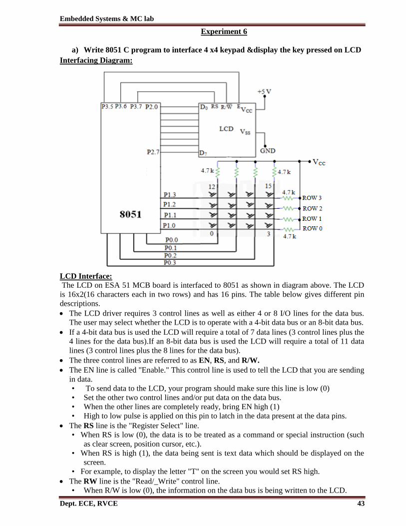
Experiment 6
a) Write 8051 C program to interface 4 x4 keypad &display the key pressed on LCD
Interfacing Diagram:
LCD Interface:
The LCD on ESA 51 MCB board is interfaced to 8051 as shown in diagram above. The LCD
is 16x2(16 characters each in two rows) and has 16 pins. The table below gives different pin
descriptions.
The LCD driver requires 3 control lines as well as either 4 or 8 I/O lines for the data bus.
The user may select whether the LCD is to operate with a 4-bit data bus or an 8-bit data bus.
If a 4-bit data bus is used the LCD will require a total of 7 data lines (3 control lines plus the
4 lines for the data bus).If an 8-bit data bus is used the LCD will require a total of 11 data
lines (3 control lines plus the 8 lines for the data bus).
The three control lines are referred to as EN, RS, and R/W.
The EN line is called "Enable." This control line is used to tell the LCD that you are sending
in data.
• To send data to the LCD, your program should make sure this line is low (0)
• Set the other two control lines and/or put data on the data bus.
• When the other lines are completely ready, bring EN high (1)
• High to low pulse is applied on this pin to latch in the data present at the data pins.
The RS line is the "Register Select" line.
• When RS is low (0), the data is to be treated as a command or special instruction (such
as clear screen, position cursor, etc.).
• When RS is high (1), the data being sent is text data which should be displayed on the
screen.
• For example, to display the letter "T" on the screen you would set RS high.
The RW line is the "Read/_Write" control line.
• When R/W is low (0), the information on the data bus is being written to the LCD.
Embedded Systems & MC lab
Dept. ECE, RVCE 44
• When R/W is high (1), the program is effectively querying (or reading) the LCD.
• Only one instruction (reading LCD status) is a read command. The busy flag(D7)
combined R/W & RS is used to read LCD status. If R/W=1 ,RS =0 if D7=1(busy
flag=1) the LCD is busy taking care of internal operations and will not accept any new
operation. When D7=0, the LCD is ready to receive new information. It is
recommended to check the busy flag before writing any data to the LCD.
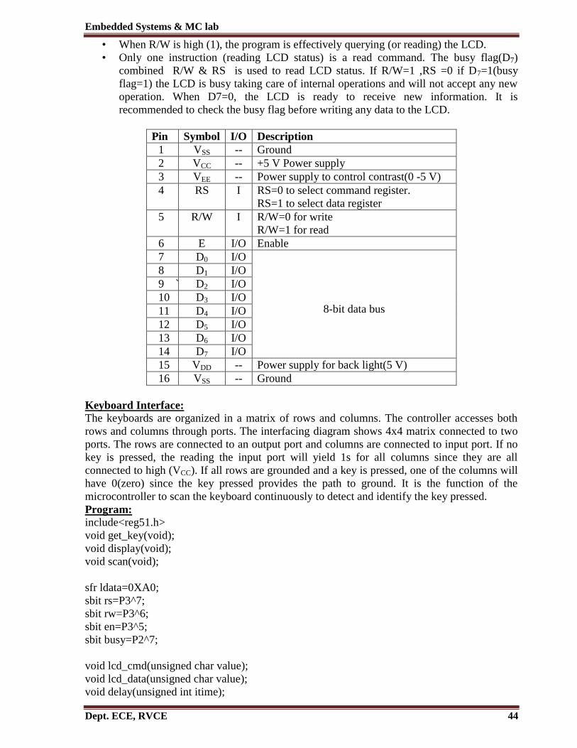
Pin Symbol I/O Description
1 VSS -- Ground
2 VCC -- +5 V Power supply
3 VEE -- Power supply to control contrast(0 -5 V)
4 RS I RS=0 to select command register.
RS=1 to select data register
5 R/W I R/W=0 for write
R/W=1 for read
6 E I/O Enable
7 D0 I/O
8-bit data bus
8 D1 I/O
9 ` D2 I/O
10 D3 I/O
11 D4 I/O
12 D5 I/O
13 D6 I/O
14 D7 I/O
15 VDD -- Power supply for back light(5 V)
16 VSS -- Ground
Keyboard Interface:
The keyboards are organized in a matrix of rows and columns. The controller accesses both
rows and columns through ports. The interfacing diagram shows 4x4 matrix connected to two
ports. The rows are connected to an output port and columns are connected to input port. If no
key is pressed, the reading the input port will yield 1s for all columns since they are all
connected to high (VCC). If all rows are grounded and a key is pressed, one of the columns will
have 0(zero) since the key pressed provides the path to ground. It is the function of the
microcontroller to scan the keyboard continuously to detect and identify the key pressed.
Program:
include<reg51.h>
void get_key(void);
void display(void);
void scan(void);
sfr ldata=0XA0;
sbit rs=P3^7;
sbit rw=P3^6;
sbit en=P3^5;
sbit busy=P2^7;
void lcd_cmd(unsigned char value);
void lcd_data(unsigned char value);
void delay(unsigned int itime);

Embedded Systems & MC lab
Dept. ECE, RVCE 45
void lcd_ready();
idata temp2,temp3,flag,row,res1;
void main ()
lcd_cmd(0x38); // 8 BIT DATA , 2LINE, 5X7 DOT MATRIX
lcd_cmd(0x0E); // DISPLAY ON, CURSOR ON, NO BLINK
lcd_cmd(0x01); //CLEAR DISPLAY
while(1)
get_key();
display();
void get_key(void)
flag =0x00;
while(1)
for(row=0;row<4;row++)
if(row==0)
temp3=0xfe;
else if(row==1)
temp3=0xfd;
else if(row==2)
temp3=0xfb;
else if(row==3)
temp3=0xf7;
P1=temp3;
scan();
delay(10);
if(flag==0xff)
break;
if(flag==0xff)
break;
void scan(void)
unsigned char t;
P0=0xff;
Embedded Systems & MC lab
Dept. ECE, RVCE 46
temp2=P0;
temp2=temp2&0x0f;
if(temp2!=0x0f)
delay(30);
delay(30);
temp2=P0;
temp2=temp2&0x0f;
if(temp2!=0x0f)
flag=0xff;
res1=temp2;
if(temp3==0xfe && res1==0x0e)
res1='0';
if(temp3==0xfe && res1==0x0d)
res1='1';
if(temp3==0xfe && res1==0x0b)
res1='2';
if(temp3==0xfe && res1==0x07)
res1='3';
if(temp3==0xfd && res1==0x0e)
res1='4';
if(temp3==0xfd && res1==0x0d)
res1='5';
if(temp3==0xfd && res1==0x0b)
res1='6';
if(temp3==0xfd && res1==0x07)
res1='7';
if(temp3==0xfb && res1==0x0e)
res1='8';
if(temp3==0xfb && res1==0x0d)
res1='9';
if(temp3==0xfb && res1==0x0b)
res1='A';
if(temp3==0xfb && res1==0x07)
res1='B';
if(temp3==0xf7 && res1==0x0e)
res1='C';
if(temp3==0xf7 && res1==0x0d)
res1='D';
if(temp3==0xf7 && res1==0x0b)
res1='E';
if(temp3==0xf7 && res1==0x07)
res1='F';
else
flag=0x00;

Embedded Systems & MC lab
Dept. ECE, RVCE 47
void display(void)
lcd_cmd(0x01);
lcd_cmd(0x80); // FIRST LINE
delay(5);
ldata=res1;
lcd_data(ldata);
delay(5);
void lcd_cmd(unsigned char value)
lcd_ready();
ldata=value;
rs=0;
rw=0;
en=1;
delay(5);
en=0;
return;
void lcd_data(unsigned char value)
lcd_ready();
ldata=value;
rs=1;
rw=0;
en=1;
delay(5);
en=0;
return;
void lcd_ready()
busy=1;
rs=0;
rw=1;
while(busy==1)
en=0;
delay(5);
en=1;
return;
void delay(unsigned int itime)
unsigned int i,j;
for(i=0;i<itime;i++)
for(j=0;j<50;j++);

Embedded Systems & MC lab
Dept. ECE, RVCE 48
b) Write 8051 C program to interface 4 x 4 keypad & accept 4 keys consecutively and
send to serial port
Program:
#include<reg51.h>
void get_key(void);
void scan(void);
void send(unsigned char q);
void send_string();
void delay(unsigned int itime);
idata temp2,temp3,flag,row,res1;
void main ()
unsigned char t =0, arr[5];
SCON=0x50; //serial communication settings
TMOD=0x20;
TH1=-3;
TL1=-3;
TR1=1;
send_string();
for(t=0; t<4; t++)
get_key();
arr[t]= res1;
delay(150);
for(t=0; t<4; t++)
send(arr[t]);
delay(100);
while(1);
void get_key(void)
flag =0x00;
Embedded Systems & MC lab
Dept. ECE, RVCE 49
while(1)
for(row=0;row<4;row++)
if(row==0)
temp3=0xfe;
else if(row==1)
temp3=0xfd;
else if(row==2)
temp3=0xfb;
else if(row==3)
temp3=0xf7;
P1=temp3;
scan();
delay(100);
if(flag==0xff)
break;
if(flag==0xff)
break;
void scan(void)
P0=0xff;
temp2=P0;
temp2=temp2&0x0f;
if(temp2!=0x0f)
delay(100);
flag=0xff;
res1=temp2;
if(temp3==0xfe && res1==0x0e)
res1='0';
if(temp3==0xfe && res1==0x0d)
res1='1';
if(temp3==0xfe && res1==0x0b)
res1='2';
if(temp3==0xfe && res1==0x07)
res1='3';
if(temp3==0xfd && res1==0x0e)

Embedded Systems & MC lab
Dept. ECE, RVCE 50
res1='4';
if(temp3==0xfd && res1==0x0d)
res1='5';
if(temp3==0xfd && res1==0x0b)
res1='6';
if(temp3==0xfd && res1==0x07)
res1='7';
if(temp3==0xfb && res1==0x0e)
res1='8';
if(temp3==0xfb && res1==0x0d)
res1='9';
if(temp3==0xfb && res1==0x0b)
res1='A';
if(temp3==0xfb && res1==0x07)
res1='B';
if(temp3==0xf7 && res1==0x0e)
res1='C';
if(temp3==0xf7 && res1==0x0d)
res1='D';
if(temp3==0xf7 && res1==0x0b)
res1='E';
if(temp3==0xf7 && res1==0x07)
res1='F';
else
flag=0x00;
void delay(unsigned int itime)
unsigned int i,j;
for(i=0;i<itime;i++)
for(j=0;j<50;j++);
void send_string()
unsigned char temp[20]=“\nKeys Pressed:”;
char i=0;
while(temp[i]!='\0')
send(temp[i]);
i++;

Embedded Systems & MC lab
Dept. ECE, RVCE 51
void send(unsigned char q)
SBUF=q;
while(!TI);
TI=0;
Alternate exam question:
Write a program to interface 3x8 keyboard and LCD to microcontroller.
Observations to be recorded for Experiment 6
1. Allocation of program memory for a program written in ‘C’
2. Memory allocation for variables declared in C
3. Use of header files reg51.h
4. RAM locations used for stack operations in C programs
5. Use SFR data type
6. Serial baud rate generation
7. Types of LCDs
8. LCD command set
9. Baud rate Vs Bit rate
10. Null modem connection
Embedded Systems & MC lab
Dept. ECE, RVCE 52
Experiment 7
a) Write an ALP to transmit a message “RVCE IS MY COLLEGE” serially by
programming the serial port with a baud of 9600, 8-bit data with 1-start bit & 1-
stop bit.
In serial transmission as opposed to parallel transmission, one bit at a time is transmitted.
In serial asynchronous transmission, the data consists of a Start bit (high), followed by 8
bits of data to be transmitted and finally the stop bit. The byte character to be transmitted is
written into the SBUF register. It transmits the start bit. The 8-bit character is transferred
one bit at a time. The stop bit is transferred. After the transmission, the TI flag = 1
indicating the completion of transmission. Hence in the subroutine wait until TI is set.
Later clear the TI flag and continue with transmission of the next byte by writing into the
SBUF register. (The program can also be written in interrupt mode). The speed of the
serial transmission is set by the baud rate which is done with the help of timer 1.
Timer1 must be programmed in mode 2 (that is, 8-bit, auto reload).
Baud rate Calculation: Crystal freq/ (12*32) = (11.0592MHz)/(12*32) = 28800
Serial communication circuitry divides the machine cycle frequency (11.0592MHz)/(12)
by 32 before it is being used by the timer to set the baud rate.
To get 9600, 28800/3 is obtained by loading timer1 with -3 (i.e., FF – 3 = FD) for further
clock division. For 2400 baud rate, 28800/12 => -12 = F4 in TH1.
Program:
ORG 0
SJMP 30H
ORG 30H
MOV TMOD, #20h ;Timer-1, mode-2
MOV TH1, #-3h ;baud rate of 9600.
MOV SCON, #50h ;mode-1, 8 bit data,1-start bit, 1-stop bit.
SETB TR1
MOV DPTR, #MYDATA
AGN: CLR A
MOVC A, @A+DPTR
JZ STOP
ACALL SEND
INC DPTR
SJMP AGN
STOP: SJMP STOP
SEND: MOV SBUF, A
HERE: JNB TI, HERE ; monitor TI flag for completion
CLR TI
RET
MYDATA: DB "RVCE IS MY COLLEGE.",0
END

Embedded Systems & MC lab
Dept. ECE, RVCE 53
Output:
To see the result of this program, after selecting DEBUG session in the main menu use
View-> serial window #1. On running & halting the program, the data is seen in the serial
window.
b) Write an 8051 C program to transmit characters – consecutively using internal serial
interrupt and display the same on LCD interface.
#include<reg51.h>
sfr ldata=0XA0;
sbit rs=P3^7;
sbit rw=P3^6;
sbit en=P3^5;
sbit busy=P2^7;
void lcd_cmd(unsigned char value);
void lcd_data(unsigned char value);
void delay(unsigned int itime);
void lcd_ready();
void display();
unsigned char res1;
void main ()
EA=1;
ES=1;
RI=0;
lcd_cmd(0x38); // 8 BIT DATA , 2LINE, 5X7 DOT MATRIX
lcd_cmd(0x0E); // DISPLAY ON, CURSOR ON, NO BLINK
lcd_cmd(0x01); //CLEAR DISPLAY
//lcd_cmd(0x80); // FIRST LINE
SCON=0x50; //serial communication settings
TMOD=0x20;
TH1=-3;
TL1=-3;
TR1=1;
while(1);
void receive()interrupt 4
ES=0;
res1=SBUF;
display ();
RI=0;
ES=1;
void display(void)

Embedded Systems & MC lab
Dept. ECE, RVCE 54
lcd_cmd(0x01);
delay(5);
lcd_data(res1);
delay(5);
void lcd_cmd(unsigned char value)
lcd_ready();
ldata=value;
rs=0;
rw=0;
en=1;
delay(5);
en=0;
return;
void lcd_data(unsigned char value)
lcd_ready();
ldata=value;
rs=1;
rw=0;
en=1;
delay(5);
en=0;
return;
void lcd_ready()
busy=1;
rs=0;
rw=1;
while(busy==1)
en=0;
delay(5);
en=1;
return;
void delay(unsigned int itime)
unsigned int i,j;
for(i=0;i<itime;i++)
for(j=0;j<50;j++);
Embedded Systems & MC lab
Dept. ECE, RVCE 55
Activity: Write an C Program to Display 4 characters on 7 segment LED using MUX and
Ports
Observations to be recorded for Experiment 7
1. RS-232 data & Control signals
2. RJ-11 & DB-9 Connectors signal assignment
3. Synchronous & Asynchronous serial communication
4. Use of LCD ready function in the above program
5. Importance of receiving the data using serial interrupt
6. What is level converter
7. Functionality of MAX232

Embedded Systems & MC lab
Dept. ECE, RVCE 56
Experiment 8
a) Write an 8051 C program to interface ADC in polled mode.
b) Write an 8051 C program to interface ADC in interrupt mode.
The A/D conversion is a quantizing process whereby an analog signal is converted into
equivalent binary word. An ADC has n-bit resolution where n is 8, 10, 12, 16 or even 24 bits.
The higher resolution ADC provides smaller step size, where step size is the smallest change in
input analog voltage, an ADC can detect. ADC is governed by conversion time which is
defined as time taken to convert the analog input to digital value. The step size is also called as
resolution some times. The step size is defined as ratio of a change in value of input voltage
needed to change a digital output by 1 LSB. If the full scale input voltage required to cause a
digital output of all 1’s is VIFS, then resolution (step size) can be given as,
Resolution= VIFS / 2n
Where, n=no. of output bits
Quantization Error
The figure below shows transfer curve of 3 bit ADC. From the figure, it is observed that there
is an unavoidable uncertainty about the exact value of VIN for all digital output. This
uncertainty is specified as quantization error. Its value is ± ½ LSB.
ADC 816
The ADC0816, ADC0817 data acquisition component is a monolithic CMOS device
with an 8-bit analog-to-digital converter. The 8-bit A/D converter uses successive
approximation as the conversion technique. This IC has 16-channels (IN0- IN15), so that
analog signals from 16 different sources can be given. The 4 user programmable address lines
(ADD A-ADD D) select among them any time. In ADC 816, REF(+) & REF(-) set the
reference voltage. If REF(+) =5 V and REF(-)=GND, the step size is 19.53 mv(5/256). The
input analog voltage can be varied between 0(00H) to 5V(FFH). If REF(+) =2.5 V and REF(-)
=GND, the step size is 9.7 mv (2.5/256). The input analog voltage can be varied between
0(00H) to 2.5V(FFH). In the ADC target board of lab, REF(+)=5 V and REF(-)=GND (can be
changed also). We use ADD A-ADD D to select IN0 –IN15 and activate the ALE to latch in
the address. Start(SOC) is for start of conversion. EOC(end of conversion) and OE(output
enable) is to read the 8 bit digital value (Refer timing diagram).Conversion time is 100µS.
Embedded Systems & MC lab
Dept. ECE, RVCE 57
Successive Approximation Conversion Technique
The successive approximation Analog to digital converter circuit typically consists of four
chief sub circuits:
1. A sample and hold circuit to acquire the input voltage (Vin).
2. An analog voltage comparator that compares Vin to the output of the internal
DAC (digital-to-analog converter) and outputs the result of the comparison to
the successive approximation register (SAR).
3. A successive approximation register sub circuit designed to supply an
approximate digital code of Vin to the internal DAC.
4. An internal reference DAC that supplies the comparator with an analog voltage
equivalent of the digital code output of the SAR for comparison with Vin.

Embedded Systems & MC lab
Dept. ECE, RVCE 58
Consider a three-bit conversion for simplicity. The search tree for an SAR search is
illustrated below. To start a conversion cycle a three-bit digital register is first cleared, and then
loaded with the triplet 100(MSB set to1). The register state provides the input to a DAC, and
that provides a reference output. This output is compared to the analog signal to be converted,
and a decision is made whether the analog signal is greater than or less than the reference
signal.
As the tree suggests, if the analog voltage is lesser, the comparator causes the SAR to
clear MSB; otherwise, the bit is left a 1. Then the next bit is set to 1 and does the same test,
continuing this binary search until every bit in the SAR has been tested. The resulting code is
the digital approximation of the sampled input voltage and is finally output by the DAC at the
end of the conversion (EOC).
Interfacing Diagram:

Embedded Systems & MC lab
Dept. ECE, RVCE 59
a) This program demonstrates polled mode of I/O support. This program display
converted digital value on serial window. Since the program run in polling mode, the
digital value is displayed continuously. The above program can be made interrupt
driven using any one external interrupt. Mean while processor can be put in idle
mode. (as demonstrated in next program)
#include<reg51.h>
sbit sel0=P0^0;
sbit sel1=P0^1;
sbit sel2=P0^2;
sbit sel3=P0^3;
sbit ale=P0^4;
sbit soc=P0^5;
sbit rd=P0^6;
sbit eoc=P2^0;
void delay(unsigned int i)
for(;i>0;i--);
return;
void send(unsigned char q)
SBUF=q;
while(!TI);
TI=0;
void convert(unsigned char y)
unsigned char q;
q=y;
y=(y>>4)&0x0f;
if(y>0x09)
y+=0x07;
y+=0x30;
send(y);
y=q;
y=y&0x0F;
if(y>0x09)
y+=0x07;
y+=0x30;
send(y);
void send_string()
unsigned char temp[20]='\n','D','i','g','i','t','a','l',' ','v','a','l','u','e',':','\0';
char i=0;
while(temp[i]!='\0')
Embedded Systems & MC lab
Dept. ECE, RVCE 60
send(temp[i]);
i++;
delay(10000);
void main(void)
unsigned char a;
P0=0x00;
P2=0xff;
sel0=0x0;
sel1=0;
sel2=0;
sel3=0;
P1=0xff;
SCON=0x50;
TMOD=0x20;
TH1=-3;
TL1=-3;
TR1=1;
while(1)
soc=1;
delay(1000);
soc=0;
delay(10000);
while(eoc==0);
rd=1; //wait for EOC signal
a=P1;
rd=0;
send_string();
convert(a);
delay(64000);
b) Interrupt driven I/O support(reduces power consumption)
#include<reg51.h>
sbit sel0=P0^0;
sbit sel1=P0^1;
sbit sel2=P0^2;
sbit sel3=P0^3;
sbit ale=P0^4;
sbit soc=P0^5;
sbit rd=P0^6;
sbit eoc=P2^0;
unsigned char title[]='\n','D','i','g','i','t','a','l',' ','v','a','l','u','e',':','\0';
unsigned char message[]="\nCPU is in IDLE mode,Enable INT0 to continue";
void delay(unsigned int i)
Embedded Systems & MC lab
Dept. ECE, RVCE 61
for(;i>0;i--);
return;
void send(unsigned char q)
SBUF=q;
while(!TI);
TI=0;
void convert(unsigned char y)
unsigned char q;
q=y;
y=(y>>4)&0x0f;
if(y>0x09)
y+=0x07;
y+=0x30;
send(y);
y=q;
y=y&0x0F;
if(y>0x09)
y+=0x07;
y+=0x30;
send(y);
void doNothing(void)interrupt 0
//No code
void send_string(unsigned char temp[])
char i=0;
while(temp[i]!='\0')
send(temp[i]);
i++;
void main(void)
unsigned char a;
P0=0x00;
P2=0xff;
sel0=0x0;
sel1=0;

Embedded Systems & MC lab
Dept. ECE, RVCE 62
sel2=0;
sel3=0;
P1=0xff;
SCON=0x50;
TMOD=0x20;
TH1=-3;
TL1=-3;
TR1=1;
IE=0x81; //Enable external interrupt 0
while(1)
soc=1;
delay(1000);
soc=0;
while(eoc==0);
rd=1; //wait for EOC signal
a=P1;
rd=0;
send_string(title);
convert(a);
send_string(message);
PCON=0x01; //After one conversion, enable idle mode.
Observations to be recorded for Experiment 8
1. Resolution of ADC
2. Quantization error of ADC
3. ADC control signals
4. Types of ADCs(Explain briefly)
5. Use of Sleep modes of MCU

Embedded Systems & MC lab
Dept. ECE, RVCE 63
6. Idle mode of 8051 MCU
7. Methods to improve resolution of ADC
8. Parallel Vs serial ADC
9. Use of serial window of Keil
10. ADC selection criteria

Embedded Systems & MC lab
Dept. ECE, RVCE 64
EXPERIMENT 9
a) Generate PWM wave on pin P3.1 to control speed of DC motor. Control the duty
cycle by analog input.
Interfacing Diagram:
This program demonstrates the generation of pulse width modulated wave to control the speed
of DC motor. By changing (modulating) the width of the pulse applied to DC motor we can
increase or decrease the amount of power provided to the motor, thereby increasing or
decreasing motor speed. Notice that, although the voltage has fixed amplitude, it has variable
duty cycle. In this program, digital equivalent of analog input voltage is used to vary the duty
cycle using timers. Speed varies linearly with analog voltage.
Program:
#include<reg51.h>
sbit sel0=P0^0;
sbit sel1=P0^1;
sbit sel2=P0^2;
sbit sel3=P0^3;
sbit ale=P0^4;
sbit soc=P0^5;
sbit rd=P0^6;
sbit eoc=P2^0;
sbit pwm=P3^1;
void delay(unsigned int i)
for(;i>0;i--);
return;
void main(void)
unsigned char a;
P0=0x00;
P2=0xff;
sel0=0x0;
Embedded Systems & MC lab
Dept. ECE, RVCE 65
sel1=0;
sel2=0;
sel3=0;
P1=0xff;
TMOD=0x10;
TH1=0;
TL1=0;
while(1)
soc=1;
delay(1000);
soc=0;
while(eoc==0);
rd=1; //wait for EOC signal
a=P1;
rd=0;
TH1=a;
TL1=a;
TR1=1;
pwm=0;
while(TF1==0);
TF1=0;
a=~a;
TH1=a;
TL1=a;
pwm=1;
TR1=1;
while(TF1==0);
TF1=0;
b) Write a program to generate sine wave using DAC. Display the generated signal in
logic analyzer window in simulation mode and in CRO in target mode.
Interfacing diagram:

Embedded Systems & MC lab
Dept. ECE, RVCE 66
Circuit Diagram:
In DAC 0800A digital inputs are converted to current (Iout) and by connecting a current to
voltage converter output result in voltage. The total output current is function of the binary
information D0- D7 inputs of the DAC and reference current (Iref) and is given as,
Iref is the current generated by 10 V power supply and 3 KΩ resistor.
To generate a sine wave, we first need table whose values represent the magnitude of
the sine angles between 0 and 360 degrees. The values for the sine vary from -1.0 to 1.0 for 0
to 360 degrees. The table below shows the angles, the sine values, the voltage magnitudes and
integer values representing the voltage magnitude for each angle.
Angle θ Vout (Voltage Magnitude)
5 V+(5V x sin θ)
Values sent to DAC
(Vout x 25.6)
0 5 128 d (80 H)
5 5.4 139 d (8B H)
10 5.86 150 d (96 H)
15 6.29 161 d (A1 H)
20 6.79 171 d (AB H)
25 7.11 182 d (B6 H)
30 7.5 192 d (C0 H)
To generate the above table, we assumed the full scale voltage of 10 V for DAC output. Full
scale output of the DAC is achieved when all the data inputs of the DAC are high. To find the
value sent to the DAC for various angles, we simply multiply the Vout voltages by 25.6 because
there are 256 steps in 10 volts. Therefore, 256 steps/ 10 V =25.6 steps/ volt. Similar procedure
is followed to calculate the integer values for all remaining angles.
Program:
#include <REG51xD2.H>
main()

Embedded Systems & MC lab
Dept. ECE, RVCE 67
unsigned char i,
z[]=0x80,0x8b,0x96,0xa1,0xab,0xb6,0xc0,0xc9,0xd2,0xda,0xe2,0xe8,0xee,0xf4,0xf8,
0xfb,0xfe,0xff,0xfe,0xfb,0xf8,0xf4,0xee,0xe8,0xe2,0xda,0xd2,0xc9,0xc0,0xb6,0xab,0
xa1,0x96,0x8b,0x80,0x74,0x69,0x5e,0x59,0x49,0x40,0x36,0x2d,0x25,0x1d,0x17,0x1
1,0x0a,0x07,0x04,0x00,0x00,0x04,0x07,0x0a,0x11,0x17,0x1d,0x25,0x2d,0x36,0x40,0
x49,0x59,0x5e,0x69,0x74,0x80 ;
while(1) //do it for ever
for(i=0;i<67;i++)
P0=z[i];
Alternate exam question:
Write a program to generate sine wave of given frequency.
Observations to be recorded for Experiment 9
1. Use of I to V converter in DAC board
2. Use of dual DAC on Target board
3. What is peak to peak voltage of sine wave generated
4. What is reference voltage and current for DAC
5. Peace of code for generating square wave, Saw-tooth waveform
6. What is the digital equivalent of 3V analog voltage for ADC0816

Embedded Systems & MC lab
Dept. ECE, RVCE 68
EXPERIMENT 10
a) Write an 8051 C program to measure frequency of TTL waveform.
This program demonstrates use of counter to measure the frequency of TTL
waveform connected to pin P3.4.After starting counter, it is made to count for
approximately for one second. The measured frequency in Hz is displayed on interfaced
LCD in reverse order. To meet timing constraint, assembly instructions (inline assembly)
are written in C program.
Interfacing Diagram:
Program:
#include <REG51.H>
sfr ldata=0XA0;
sbit rs=P3^7;
sbit rw=P3^6;
sbit en=P3^5;
sbit busy=P2^7;
unsigned char countOverflow;
unsigned long int freq;
unsigned int count;
void calFreq();
void lcd_cmd(unsigned char value);
void lcd_data(unsigned char value);
void delay(unsigned int itime);
void lcd_ready();
void sendString();
void sendFreq();
unsigned char string[]='F','R','Q','U','E','N','C','Y',' ','M','E','T','E','R';
unsigned long int frqOffset[]=0,65536,131071,196608,262144,3276800,393216,458752;
void onCounterOverflow(void)interrupt 1

Embedded Systems & MC lab
Dept. ECE, RVCE 69
TF0=0;
countOverflow+=1;
main()
IE=0x82;
lcd_cmd(0x3C); /* 10x5 dot matrix, 2 line dislay, 8 bit data line*/
while(1)
TH0=TL0=0;
count=0;
countOverflow=0;
TMOD=0x15;
#pragma asm
MOV R0,#14
CLR A
MOV TH1,A
MOV TL1,A
MOV TH0,A
MOV TL0,A
MOV TCON,#50h
Here:JNB TF1,Here
CLR TF1
MOV R1,#91
Wait:DEC R1
CJNE R1.#00h,wait
DJNZ R0,here
CLR TR0
CLR TR1
#pragma endasm
lcd_cmd(0x01); /*clear */
sendString();
lcd_cmd(0x0C0);
calFreq();
sendFreq();
lcd_data('H');
lcd_data('z');
void sendFreq()
unsigned char temp;
while(freq!=0)
temp=freq%10;
freq/=10;
Embedded Systems & MC lab
Dept. ECE, RVCE 70
temp=temp+(0x30);
lcd_data(temp);
void calFreq()
freq=frqOffset[countOverflow];
count=TH0;
count=count<<8;
count+=TL0;
freq+=count;
void sendString()
char i;
for(i=0;i<14;i++)
lcd_data(string[i]);
void lcd_cmd(unsigned char value)
lcd_ready();
ldata=value;
rs=0;
rw=0;
en=1;
delay(5);
en=0;
return;
void lcd_data(unsigned char value)
lcd_ready();
ldata=value;
rs=1;
rw=0;
en=1;
delay(5);
en=0;
return;
void lcd_ready()
busy=1;
rs=0;
rw=1;
Embedded Systems & MC lab
Dept. ECE, RVCE 71
while(busy==1)
en=0;
delay(5);
en=1;
return;
void delay(unsigned int itime)
unsigned int i,j;
for(i=0;i<itime;i++)
for(j=0;j<50;j++);
Note: Before compiling, Select Generate Assembler SRC file & Assemble SRC file under
options for source group1 and add C51S library file to project (path: source
drive\Keil\C51\LIB).
Observations to be recorded for Experiment 10
1. Inline Assembly
2. Situations demanding inline assembly
3. Keil optimization tools
4. DAC 0800
5. Compare IDLE mode with NOP instructions.
6. Use of adding C51S library file to the program

Embedded Systems & MC lab
Dept. ECE, RVCE 72
DEPARTMENT OF ELECTRONICS AND COMMUNICATION
R.V. COLLEGE OF ENGINEERING, BANGALORE – 59.
Embedded systems & Microcontrollers Lab
Viva –Voce Questions
1. Differentiate between RISC & CISC.
2. What is hardwired control unit?
3. What is micro programmed control unit?
4. Mention different ways to implement processor register.
5. What is the meaning of hardware support & software support for an instruction?
6. Differentiate between microprocessor & microcontroller.
7. What is embedded system?
8. Differentiate between hard & soft embedded systems with examples.
9. What is real time embedded systems.
10. Mention important constraints of embedded systems.
11. Why RISC processors are called load & store architectures?
12. Differentiate between Von Neuman & Harvard architectures with examples.
13. Compare clock speeds of microprocessor & microcontroller.
14. What is general purpose processor?
15. Mention qualifying factors of microcontroller for an embedded system.
16. Mention variants of 8051 microcontroller.
17. What is instruction set compatibility?
18. What is the driving capability of 8051 microcontroller ports?
19. What is orthogonal instruction set?
20. What is power on reset?
21. How reset action of 8051 is initiated?
22. What is minimum & maximum clock frequency of Intel’s 8051?
23. Differentiate between instruction cycle, machine cycle & clock cycle?
24. Why AT89C51ED2 is operated at 11.0592 MHz?
25. Explain naming convention of AT89C51ED2.
26. Why the crystal oscillator used to drive MCUs?
27. Why the machine cycle width of AT89C51ED2 is 12 clock cycles (probable reason)?
28. Explain data memory organization of Intel’s 8051.
29. Mention the advantages of bit addressable locations.
30. Mention the advantages of bit addressable locations with context to program memory.
31. Explain data memory organization of AT89C51ED2.
32. Explain interfacing of external data memory with timing diagram.
33. Explain organization of the program memory in Intel’s 8051?
34. What is the status of PSEN signal to access on chip ROM?
35. What is the status of EA pin to access on chip data RAM?
36. How microcontroller differentiates between on chip & off chip data memory access?
37. Show the flag register status after execution of (23h-77h) operation.
38. Show interfacing of 4K x 8 ROM chip to 8051 microcontroller.
39. Write instruction to move the stack above 80h location.
40. Mention different units of ports.

Embedded Systems & MC lab
Dept. ECE, RVCE 73
41. The data memory of AT89C51ED2 is 256(00-FFh) bytes. The SFRs are also
implemented in RAM locations 80-FFh. Write instructions to RAM locations & SFRs.
42. How to test stack overflow?
43. Differentiate between directive & instruction.
44. What is read-modify-write instruction?
45. The ALE signal is generated twice/machine cycle. Two bytes are fetched though an
instruction is 1 byte which takes atleast 1MC to execute. Will the second byte is decoded?
46. Differentiate between reading a latch & reading a pin with examples.
47. Mention different ways to support I/O devices.
48. Explain port 0 pin structure.
49. Differentiate between bidirectional & quasi bidirectional port with examples.
50. Write a program to read the status of switch & actuating LED continuously. Use
directives.
51. Write instruction to configure a port as output.
52. What is the fan out of port pins of 8051microcontoller?
53. Why external pull up resistor is required for I/O operation of port 0?
54. Differentiate between QFP & DIP ICs.
55. What is advantage of fixed length instructions of RISC architectures?
56. Differentiate between timer & counter with an example each.
57. Mention different ways to generate delay using 8051 microcontroller.
58. Mention different ways to control timer/counter running.
59. If the input oscillator frequency is 11.0592 MHz, then what is the TL0 counter
frequency?
60. Explain auto reload counter mode of 8051.
61. Write a program to generate delay of 1sec using timer1 in any mode.
62. Write an ISR of timer 1 to read a switch every 100ms.
63. Explain mode 3 of timer 0.
64. What is the maximum input frequency that can be accurately counted by an
AT89C51ED2 controller counter at XTAL=16MHz ?
65. Explain TMOD register.
66. Write a program to generate a square wave of 100 KHz &70% duty cycle using delay
loop.
67. What is watch dog timer? Mention some probable reasons causing hanging of system.
68. How to control the running of timer 1 if timer 0 is set in mode 3?
69. If the input oscillator frequency is 11.0592 MHz, then what is the TH counter
frequency in mode 0 & mode 1?
70. What is the application GATE bit of timer/counter?
71. Mention different conditions which set overflow flag to 0.
72. What is the advantage of bit addressable registers? Explain with examples.
73. Explain control logic of timer/counter.
74. The timer 1 is programmed in mode 2. The value in TH0 register is F3h. What is the
initial state for first counting sequence?
75. What is wake up time of 8051?

Embedded Systems & MC lab
Dept. ECE, RVCE 74
76. Design an 8051 based system to measure the pulse width. It is learnt that the pulse to
be measured is generated at random interval of times. Use sleep mode of 8051 to reduce
power consumption.
77. Explain power saving modes of 8051.
78. Differentiate between parallel & serial data transfer with examples.
79. Differentiate between synchronous & asynchronous serial communication with
examples.
80. What is block data transfer?
81. What is baud rate? Compare with bps.
82. Explain simplex, half duplex & full duplex serial communication.
83. Explain data transmission formats of synchronous & asynchronous transmission.
84. What is master-slave configuration?
85. What is RS-232? Explain voltage levels RS-232.
86. Explain 9 signals of RS-232.
87. Explain Null modem connection of RS-232.
88. Mention advantages of high voltage levels of RS-232.
89. Mention different methods to support serial communication with merits & demerits.
90. Explain the registers of 8051 used for serial communication.
91. Explain shift register mode of 8051.
92. The mode 0 of serial interface is half duplex synchronous transmission. Explain how
direction of data flow is controlled in this mode.
93. What is the baud rate of mode 0?
94. What is UART? Explain how baud rate is generated in this mode.
95. The timer 0 is configured in mode 3 & timer 1 in mode 1. To generate the baud timer 1
can be used or not?
96. What is multiprocessor communication mode?
97. What is framing error? Explain the support available in 8051 to detect framing error in
serial mode 1.
98. Design a scheme for connecting 3 8051 microcontrollers using full duplex serial
communication with variable baud rate. Select any one controller as a master and assign
address to slaves. Write block diagram showing connection of controllers. It is learnt that
master communicate with a salve every 10ms. Write ALP for master for this communication.
99. Explain interrupts of 8051.
100. Explain different actions performed by microcontroller upon arrival of interrupts.
101. Mention different priority levels among 8051 interrupts.
102. How contention among multiples interrupts of same priorities is solved in 8051?
103. Interrupt driven I/O support is better than polling. Why?
104. What is the minimum response time 8051 interrupt?
105. Differentiate between edge triggered & level triggered interrupts.
106. Write an assembly program to generate square wave of 2 KHz square wave & 50%
duty cycle using timer interrupts.
107. Why some time interrupts may have high response time?
108. Explain how hardware single stepping is implemented using interrupts.
109. Write a C program to transmit message “My best friend” serially. Use serial interrupt.
Embedded Systems & MC lab
Dept. ECE, RVCE 75
110. Write a C program to send actuating signal to a bell for every 1 second.
111. Which are the addressing modes supported by 8051.Explain with examples.
112. Explain instruction formats of 8051.
113. Differentiate between MOVX & MOVC instructions.
114. MOV A,80h & MOV A,P0 are the instructions doing same job. Differentiate between
these two instructions with respect to assembling time.
115. Write an instruction to push the accumulator on stack.
116. What is DB? Write program statements to store string “Microcontroller” at memory
locations starting at 500h.
117. What is EQU directive? Explain with an example.
118. Why all the programs are instructed to start at program memory locations above 30h?
119. Why END is the last statement of program? What is the machine code for the same?
120. Why the statement Here: SJMP Here required in all programs?
121. What is listing file?
122. Differentiate between .obj & .abs files?
123. What is object to hex converter?
124. What Intel hex file? Why these files are required?
125. Write a program to copy the value 55h into RAM locations 40h to 45h using
a)Immediate addressing mode
b)indirect addressing mode without a loop c) with a loop
126. Write program to copy the internal code byte at address 0300h to external RAM
address 0300h.
127. Explain internal RAM organization of AT89C51Ed2? How accessing of SFRs is
differentiated compare to upper 128 bytes of RAM?
128. Write a program to demonstrate the use of MOVC instruction.
129. Write instruction to move content of any upper 128 bytes of RAM locations of
AT89C51ED2.
130. Explain the following instruction. XCH A,P0
131. Show that set of XCH instructions executes faster than PUSH & POP when saving
contents of A register.
132. Write the instructions to do the following
a) Complement the contents of RAM location 30H
b) Mask upper four bits of A
c) Set lower 4 bits of A
133. What is the operation of following instructions?
Mybit equ p1.0
mov c, Mybit
mov r0,#Mybit
134. What is the operation of following instructions?
In_port equ p1
mov r1,In_port
mov r0,#In_port
135. A switch is connected to pin P1.7 and LED to pin P2.0. Write a program to get the
status of the switch and send it to LED.
Embedded Systems & MC lab
Dept. ECE, RVCE 76
136. Explain rotate instructions. Write program to transfer accumulator contents serially to
some peripheral connected to port pins.
137. Write a program to add 2 16-bit numbers FC45h and 02ECh.
138. Explain DA instruction with an example.
139. How DIV instruction indicates divide-by-zero error?
140. Write syntax instruction of unconditional jump instruction.
141. Explain SJMP, AJMP & LJMP instructions with examples.
142. Differentiate between call & Jump instructions.
143. Write a program to count number of 1’s in any number in register B and put the count
in R5.
144. Compare IDLE mode with NOP instructions.
145. Explain data types supported by 8051 C compiler of Keil.
146. Write C instruction to store string “Microcontroller” in code memory.
147. What is resolution of ADC? How resolution of ADC can be varied?
148. What is the digital equivalent of 3V analog voltage? Assume ADC is 0816 & reference
voltage is 5V.
149. What is quantization error of ADC? Explain methods to reduce it.
150. Explain successive approximation method of analog to digital conversion.
151. What is resolution of DAC?
152. Explain different stepper motors.
153. What is step angle & pitch of stepper motor?
154. Write block diagram showing connection between Keil IDE running on host system &
ESA MCB-51 target board.
155. Explain different units of Keil μVision.
156. What is In-System-Programming? What is boot loader or serial loader?
157. Compare MIPS, MFLOPS & MMACS.
158. What is code banking? Explain support provided by Keil IDE for code banking.
159. Which are the different code optimization techniques available in Keil IDE?
160. Differentiate between basic linker & extended linker of Keil.
161. What is monitor program?
162. Explaining programming 8051 program memory with diagram.
163. What are lock bits? Explain various options which could be obtained by programming
lock bits.
164. How the memory map to linker is given in the case of C programs?
165. Explain DB 9 & RJ 11 connector details.
166. Explain some features of AT89C51ED2.
167. Why we must check serial interrupt of Keil Monitor-51 driver settings?
168. Why we must not check serial interrupt of Keil monitor-51 driver settings if the
application is using serial interrupt?
169. What is the difference between reset option given in Keil IDE & hardware reset of the
MCU?
170. What is Flash memory? Compare with EEPROM.