mc68hc705c8a, mc68hsc705c8a technical data...
TRANSCRIPT
F
ree
sca
le S
em
ico
nd
uc
tor,
I
Freescale Semiconductor, Inc.n
c..
.
M68HC05Microcontrollers
MC68HC705C8A/DRev. 3, 3/2002
MC68HC705C8AMC68HSC705C8A
Technical Data
For More Information On This Product,
Go to: www.freescale.com

F
ree
sca
le S
em
ico
nd
uc
tor,
I
Freescale Semiconductor, Inc.n
c..
.
For More Information On This Product,
Go to: www.freescale.com

F
ree
sca
le S
em
ico
nd
uc
tor,
IFreescale Semiconductor, Inc.
nc
...
MC68HC705C8AMC68HSC705C8ATechnical Data
To provide the most up-to-date information, the revision of our documents on the World Wide Web will be the most current. Your printed copy may be an earlier revision. To verify you have the latest information available, refer to:
http://www.freescale.com
The following revision history table summarizes changes contained in this document. For your convenience, the page number designators have been linked to the appropriate location.
0&+&&$² 5HY 7HFKQLFDO'DWD
For More Information On This Product,
Go to: www.freescale.com
Technical Data
F
ree
sca
le S
em
ico
nd
uc
tor,
I
Freescale Semiconductor, Inc.n
c..
.
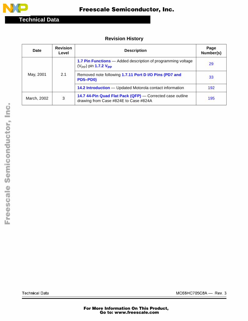
Revision History
DateRevision
LevelDescription
PageNumber(s)
May, 2001 2.1
1.7 Pin Functions — Added description of programming voltage (VPP) pin 1.7.2 VPP
29
Removed note following 1.7.11 Port D I/O Pins (PD7 and PD5–PD0)
33
14.2 Introduction — Updated Motorola contact information 192
March, 2002 314.7 44-Pin Quad Flat Pack (QFP) — Corrected case outline drawing from Case #824E to Case #824A
195
7HFKQLFDO'DWD 0&+&&$² 5HY
For More Information On This Product,
Go to: www.freescale.com

F
ree
sca
le S
em
ico
nd
uc
tor,
IFreescale Semiconductor, Inc.
nc
...
Technical Data — MC68HC705C8A
List of Sections
Section 1. General Description . . . . . . . . . . . . . . . . . . . .21
Section 2. Memory . . . . . . . . . . . . . . . . . . . . . . . . . . . . . .35
Section 3. Central Processor Unit (CPU) . . . . . . . . . . . .43
Section 4. Interrupts . . . . . . . . . . . . . . . . . . . . . . . . . . . . .49
Section 5. Resets . . . . . . . . . . . . . . . . . . . . . . . . . . . . . . .61
Section 6. Low-Power Modes. . . . . . . . . . . . . . . . . . . . . .69
Section 7. Parallel Input/Output (I/O). . . . . . . . . . . . . . . .77
Section 8. Capture/Compare Timer . . . . . . . . . . . . . . . . .89
Section 9. EPROM/OTPROM (PROM) . . . . . . . . . . . . . .103
Section 10. Serial Communications Interface (SCI). . . 121
Section 11. Serial Peripheral Interface (SPI). . . . . . . . . 139
Section 12. Instruction Set . . . . . . . . . . . . . . . . . . . . . . . 153
Section 13. Electrical Specifications . . . . . . . . . . . . . .171
Section 14. Mechanical Specifications . . . . . . . . . . . . . 191
Section 15. Ordering Information . . . . . . . . . . . . . . . . . 199
Appendix A. MC68HSC705C8A . . . . . . . . . . . . . . . . . . .201
Index. . . . . . . . . . . . . . . . . . . . . . . . . . . . . . . . . . . . . . . . .211
MC68HC705C8A — Rev. 3 Technical Data
MOTOROLA List of Sections For More Information On This Product,
Go to: www.freescale.com

List of Sections
F
ree
sca
le S
em
ico
nd
uc
tor,
I
Freescale Semiconductor, Inc.n
c..
.
Technical Data MC68HC705C8A — Rev. 3
6 List of Sections For More Information On This Product,
Go to: www.freescale.com

F
ree
sca
le S
em
ico
nd
uc
tor,
IFreescale Semiconductor, Inc.
nc
...
Technical Data — MC68HC705C8A
Table of Contents
Section 1. General Description
1.1 Contents . . . . . . . . . . . . . . . . . . . . . . . . . . . . . . . . . . . . . . . . . .21
1.2 Introduction . . . . . . . . . . . . . . . . . . . . . . . . . . . . . . . . . . . . . . . .22
1.3 Features . . . . . . . . . . . . . . . . . . . . . . . . . . . . . . . . . . . . . . . . . .22
1.4 Programmable Options. . . . . . . . . . . . . . . . . . . . . . . . . . . . . . .23
1.5 Block Diagram . . . . . . . . . . . . . . . . . . . . . . . . . . . . . . . . . . . . .24
1.6 Pin Assignments . . . . . . . . . . . . . . . . . . . . . . . . . . . . . . . . . . . .26
1.7 Pin Functions . . . . . . . . . . . . . . . . . . . . . . . . . . . . . . . . . . . . . .291.7.1 VDD and VSS. . . . . . . . . . . . . . . . . . . . . . . . . . . . . . . . . . . . .291.7.2 VPP . . . . . . . . . . . . . . . . . . . . . . . . . . . . . . . . . . . . . . . . . . . .291.7.3 OSC1 and OSC2 . . . . . . . . . . . . . . . . . . . . . . . . . . . . . . . . .301.7.4 External Reset Pin (RESET) . . . . . . . . . . . . . . . . . . . . . . . .321.7.5 External Interrupt Request Pin (IRQ) . . . . . . . . . . . . . . . . . .321.7.6 Input Capture Pin (TCAP) . . . . . . . . . . . . . . . . . . . . . . . . . .321.7.7 Output Compare Pin (TCMP) . . . . . . . . . . . . . . . . . . . . . . . .331.7.8 Port A I/O Pins (PA7–PA0). . . . . . . . . . . . . . . . . . . . . . . . . .331.7.9 Port B I/O Pins (PB7–PB0). . . . . . . . . . . . . . . . . . . . . . . . . .331.7.10 Port C I/O Pins (PC7–PC0) . . . . . . . . . . . . . . . . . . . . . . . . .331.7.11 Port D I/O Pins (PD7 and PD5–PD0) . . . . . . . . . . . . . . . . . .33
Section 2. Memory
2.1 Contents . . . . . . . . . . . . . . . . . . . . . . . . . . . . . . . . . . . . . . . . . .35
2.2 Introduction . . . . . . . . . . . . . . . . . . . . . . . . . . . . . . . . . . . . . . . .35
2.3 Memory Map. . . . . . . . . . . . . . . . . . . . . . . . . . . . . . . . . . . . . . .35
2.4 Input/Output (I/O) . . . . . . . . . . . . . . . . . . . . . . . . . . . . . . . . . . .36
MC68HC705C8A — Rev. 3 Technical Data
MOTOROLA Table of Contents For More Information On This Product,
Go to: www.freescale.com

Table of Contents
F
ree
sca
le S
em
ico
nd
uc
tor,
I
Freescale Semiconductor, Inc.n
c..
.
2.5 RAM . . . . . . . . . . . . . . . . . . . . . . . . . . . . . . . . . . . . . . . . . . . . .36
2.6 EPROM/OTPROM (PROM) . . . . . . . . . . . . . . . . . . . . . . . . . . .37
2.7 Bootloader ROM. . . . . . . . . . . . . . . . . . . . . . . . . . . . . . . . . . . .37
Section 3. Central Processor Unit (CPU)
3.1 Contents . . . . . . . . . . . . . . . . . . . . . . . . . . . . . . . . . . . . . . . . . .43
3.2 Introduction . . . . . . . . . . . . . . . . . . . . . . . . . . . . . . . . . . . . . . . .43
3.3 CPU Registers . . . . . . . . . . . . . . . . . . . . . . . . . . . . . . . . . . . . .443.3.1 Accumulator . . . . . . . . . . . . . . . . . . . . . . . . . . . . . . . . . . . .453.3.2 Index Register . . . . . . . . . . . . . . . . . . . . . . . . . . . . . . . . . . .453.3.3 Stack Pointer . . . . . . . . . . . . . . . . . . . . . . . . . . . . . . . . . . . .463.3.4 Program Counter . . . . . . . . . . . . . . . . . . . . . . . . . . . . . . . . .463.3.5 Condition Code Register . . . . . . . . . . . . . . . . . . . . . . . . . . .47
3.4 Arithmetic/Logic Unit (ALU) . . . . . . . . . . . . . . . . . . . . . . . . . . .48
Section 4. Interrupts
4.1 Contents . . . . . . . . . . . . . . . . . . . . . . . . . . . . . . . . . . . . . . . . . .49
4.2 Introduction . . . . . . . . . . . . . . . . . . . . . . . . . . . . . . . . . . . . . . . .49
4.3 Interrupt Sources . . . . . . . . . . . . . . . . . . . . . . . . . . . . . . . . . . .504.3.1 Software Interrupt. . . . . . . . . . . . . . . . . . . . . . . . . . . . . . . . .504.3.2 External Interrupt (IRQ) . . . . . . . . . . . . . . . . . . . . . . . . . . . .514.3.3 Port B Interrupts . . . . . . . . . . . . . . . . . . . . . . . . . . . . . . . . . .534.3.4 Capture/Compare Timer Interrupts . . . . . . . . . . . . . . . . . . .554.3.5 SCI Interrupts . . . . . . . . . . . . . . . . . . . . . . . . . . . . . . . . . . . .554.3.6 SPI Interrupts . . . . . . . . . . . . . . . . . . . . . . . . . . . . . . . . . . . .56
4.4 Interrupt Processing . . . . . . . . . . . . . . . . . . . . . . . . . . . . . . . . .57
Section 5. Resets
5.1 Contents . . . . . . . . . . . . . . . . . . . . . . . . . . . . . . . . . . . . . . . . . .61
5.2 Introduction . . . . . . . . . . . . . . . . . . . . . . . . . . . . . . . . . . . . . . . .61
Technical Data MC68HC705C8A — Rev. 3
8 Table of Contents For More Information On This Product,
Go to: www.freescale.com

Table of Contents
F
ree
sca
le S
em
ico
nd
uc
tor,
I
Freescale Semiconductor, Inc.n
c..
.
5.3 Reset Sources . . . . . . . . . . . . . . . . . . . . . . . . . . . . . . . . . . . . .615.3.1 Power-On Reset (POR) . . . . . . . . . . . . . . . . . . . . . . . . . . . .625.3.2 External Reset . . . . . . . . . . . . . . . . . . . . . . . . . . . . . . . . . . .625.3.3 Programmable and Non-Programmable
COP Watchdog Resets . . . . . . . . . . . . . . . . . . . . . . . . . .625.3.4 Clock Monitor Reset . . . . . . . . . . . . . . . . . . . . . . . . . . . . . . .67
Section 6. Low-Power Modes
6.1 Contents . . . . . . . . . . . . . . . . . . . . . . . . . . . . . . . . . . . . . . . . . .69
6.2 Introduction . . . . . . . . . . . . . . . . . . . . . . . . . . . . . . . . . . . . . . . .69
6.3 Stop Mode . . . . . . . . . . . . . . . . . . . . . . . . . . . . . . . . . . . . . . . .696.3.1 SCI During Stop Mode . . . . . . . . . . . . . . . . . . . . . . . . . . . . .716.3.2 SPI During Stop Mode . . . . . . . . . . . . . . . . . . . . . . . . . . . . .716.3.3 Programmable COP Watchdog in Stop Mode . . . . . . . . . . .716.3.4 Non-Programmable COP Watchdog in Stop Mode . . . . . . .73
6.4 Wait Mode. . . . . . . . . . . . . . . . . . . . . . . . . . . . . . . . . . . . . . . . .736.4.1 Programmable COP Watchdog in Wait Mode . . . . . . . . . . .756.4.2 Non-Programmable COP Watchdog in Wait Mode . . . . . . .75
6.5 Data-Retention Mode . . . . . . . . . . . . . . . . . . . . . . . . . . . . . . . .75
Section 7. Parallel Input/Output (I/O)
7.1 Contents . . . . . . . . . . . . . . . . . . . . . . . . . . . . . . . . . . . . . . . . . .77
7.2 Introduction . . . . . . . . . . . . . . . . . . . . . . . . . . . . . . . . . . . . . . . .77
7.3 Port A . . . . . . . . . . . . . . . . . . . . . . . . . . . . . . . . . . . . . . . . . . . .787.3.1 Port A Data Register . . . . . . . . . . . . . . . . . . . . . . . . . . . . . .787.3.2 Data Direction Register A. . . . . . . . . . . . . . . . . . . . . . . . . . .797.3.3 Port A Logic . . . . . . . . . . . . . . . . . . . . . . . . . . . . . . . . . . . . .80
7.4 Port B . . . . . . . . . . . . . . . . . . . . . . . . . . . . . . . . . . . . . . . . . . . .817.4.1 Port B Data Register . . . . . . . . . . . . . . . . . . . . . . . . . . . . . .817.4.2 Data Direction Register B. . . . . . . . . . . . . . . . . . . . . . . . . . .827.4.3 Port B Logic . . . . . . . . . . . . . . . . . . . . . . . . . . . . . . . . . . . . .83
MC68HC705C8A — Rev. 3 Technical Data
MOTOROLA Table of Contents For More Information On This Product,
Go to: www.freescale.com

Table of Contents
F
ree
sca
le S
em
ico
nd
uc
tor,
I
Freescale Semiconductor, Inc.n
c..
.
7.5 Port C . . . . . . . . . . . . . . . . . . . . . . . . . . . . . . . . . . . . . . . . . . . .857.5.1 Port C Data Register . . . . . . . . . . . . . . . . . . . . . . . . . . . . . .857.5.2 Data Direction Register C. . . . . . . . . . . . . . . . . . . . . . . . . . .867.5.3 Port C Logic . . . . . . . . . . . . . . . . . . . . . . . . . . . . . . . . . . . . .87
7.6 Port D . . . . . . . . . . . . . . . . . . . . . . . . . . . . . . . . . . . . . . . . . . . .88
Section 8. Capture/Compare Timer
8.1 Contents . . . . . . . . . . . . . . . . . . . . . . . . . . . . . . . . . . . . . . . . . .89
8.2 Introduction . . . . . . . . . . . . . . . . . . . . . . . . . . . . . . . . . . . . . . . .89
8.3 Timer Operation . . . . . . . . . . . . . . . . . . . . . . . . . . . . . . . . . . . .898.3.1 Input Capture . . . . . . . . . . . . . . . . . . . . . . . . . . . . . . . . . . . .928.3.2 Output Compare. . . . . . . . . . . . . . . . . . . . . . . . . . . . . . . . . .93
8.4 Timer I/O Registers. . . . . . . . . . . . . . . . . . . . . . . . . . . . . . . . . .948.4.1 Timer Control Register . . . . . . . . . . . . . . . . . . . . . . . . . . . . .948.4.2 Timer Status Register . . . . . . . . . . . . . . . . . . . . . . . . . . . . .968.4.3 Timer Registers . . . . . . . . . . . . . . . . . . . . . . . . . . . . . . . . . .978.4.4 Alternate Timer Registers. . . . . . . . . . . . . . . . . . . . . . . . . . .988.4.5 Input Capture Registers . . . . . . . . . . . . . . . . . . . . . . . . . .1008.4.6 Output Compare Registers. . . . . . . . . . . . . . . . . . . . . . . . .101
Section 9. EPROM/OTPROM (PROM)
9.1 Contents . . . . . . . . . . . . . . . . . . . . . . . . . . . . . . . . . . . . . . . . .103
9.2 Introduction . . . . . . . . . . . . . . . . . . . . . . . . . . . . . . . . . . . . . . .103
9.3 EPROM/OTPROM (PROM) Programming . . . . . . . . . . . . . . .1049.3.1 Program Register . . . . . . . . . . . . . . . . . . . . . . . . . . . . . . . .1099.3.2 Preprogramming Steps . . . . . . . . . . . . . . . . . . . . . . . . . . .110
9.4 PROM Programming Routines . . . . . . . . . . . . . . . . . . . . . . . .1119.4.1 Program and Verify PROM. . . . . . . . . . . . . . . . . . . . . . . . .1119.4.2 Verify PROM Contents . . . . . . . . . . . . . . . . . . . . . . . . . . . .1129.4.3 Secure PROM . . . . . . . . . . . . . . . . . . . . . . . . . . . . . . . . . .1129.4.4 Secure PROM and Verify . . . . . . . . . . . . . . . . . . . . . . . . . .1139.4.5 Secure PROM and Dump. . . . . . . . . . . . . . . . . . . . . . . . . .1139.4.6 Load Program into RAM and Execute . . . . . . . . . . . . . . . .114
Technical Data MC68HC705C8A — Rev. 3
10 Table of Contents For More Information On This Product,
Go to: www.freescale.com

Table of Contents
F
ree
sca
le S
em
ico
nd
uc
tor,
I
Freescale Semiconductor, Inc.n
c..
.
9.4.7 Execute Program in RAM. . . . . . . . . . . . . . . . . . . . . . . . . .1159.4.8 Dump PROM Contents. . . . . . . . . . . . . . . . . . . . . . . . . . . .115
9.5 Control Registers . . . . . . . . . . . . . . . . . . . . . . . . . . . . . . . . . .1169.5.1 Option Register . . . . . . . . . . . . . . . . . . . . . . . . . . . . . . . . .1169.5.2 Mask Option Register 1 . . . . . . . . . . . . . . . . . . . . . . . . . . .1179.5.3 Mask Option Register 2 . . . . . . . . . . . . . . . . . . . . . . . . . . .118
9.6 EPROM Erasing . . . . . . . . . . . . . . . . . . . . . . . . . . . . . . . . . . .119
Section 10. Serial Communications Interface (SCI)
10.1 Contents . . . . . . . . . . . . . . . . . . . . . . . . . . . . . . . . . . . . . . . . .121
10.2 Introduction . . . . . . . . . . . . . . . . . . . . . . . . . . . . . . . . . . . . . . .121
10.3 Features . . . . . . . . . . . . . . . . . . . . . . . . . . . . . . . . . . . . . . . . .122
10.4 SCI Data Format. . . . . . . . . . . . . . . . . . . . . . . . . . . . . . . . . . .122
10.5 SCI Operation . . . . . . . . . . . . . . . . . . . . . . . . . . . . . . . . . . . . .12310.5.1 Transmitter . . . . . . . . . . . . . . . . . . . . . . . . . . . . . . . . . . . . .12310.5.2 Receiver . . . . . . . . . . . . . . . . . . . . . . . . . . . . . . . . . . . . . . .127
10.6 SCI I/O Registers . . . . . . . . . . . . . . . . . . . . . . . . . . . . . . . . . .12910.6.1 SCI Data Register . . . . . . . . . . . . . . . . . . . . . . . . . . . . . . .12910.6.2 SCI Control Register 1 . . . . . . . . . . . . . . . . . . . . . . . . . . . .13010.6.3 SCI Control Register 2 . . . . . . . . . . . . . . . . . . . . . . . . . . . .13110.6.4 SCI Status Register . . . . . . . . . . . . . . . . . . . . . . . . . . . . . .13310.6.5 Baud Rate Register . . . . . . . . . . . . . . . . . . . . . . . . . . . . . .136
Section 11. Serial Peripheral Interface (SPI)
11.1 Contents . . . . . . . . . . . . . . . . . . . . . . . . . . . . . . . . . . . . . . . . .139
11.2 Introduction . . . . . . . . . . . . . . . . . . . . . . . . . . . . . . . . . . . . . . .139
11.3 Features . . . . . . . . . . . . . . . . . . . . . . . . . . . . . . . . . . . . . . . . .140
11.4 Operation . . . . . . . . . . . . . . . . . . . . . . . . . . . . . . . . . . . . . . . .14211.4.1 Pin Functions in Master Mode . . . . . . . . . . . . . . . . . . . . . .14311.4.2 Pin Functions in Slave Mode . . . . . . . . . . . . . . . . . . . . . . .144
11.5 Multiple-SPI Systems . . . . . . . . . . . . . . . . . . . . . . . . . . . . . . .145
MC68HC705C8A — Rev. 3 Technical Data
MOTOROLA Table of Contents For More Information On This Product,
Go to: www.freescale.com

Table of Contents
F
ree
sca
le S
em
ico
nd
uc
tor,
I
Freescale Semiconductor, Inc.n
c..
.
11.6 Serial Clock Polarity and Phase . . . . . . . . . . . . . . . . . . . . . . .146
11.7 SPI Error Conditions . . . . . . . . . . . . . . . . . . . . . . . . . . . . . . . .14711.7.1 Mode Fault Error . . . . . . . . . . . . . . . . . . . . . . . . . . . . . . . .14711.7.2 Write Collision Error . . . . . . . . . . . . . . . . . . . . . . . . . . . . . .14711.7.3 Overrun Error . . . . . . . . . . . . . . . . . . . . . . . . . . . . . . . . . . .148
11.8 SPI Interrupts . . . . . . . . . . . . . . . . . . . . . . . . . . . . . . . . . . . . .148
11.9 SPI I/O Registers . . . . . . . . . . . . . . . . . . . . . . . . . . . . . . . . . .14811.9.1 SPI Data Register. . . . . . . . . . . . . . . . . . . . . . . . . . . . . . . .14911.9.2 SPI Control Register. . . . . . . . . . . . . . . . . . . . . . . . . . . . . .14911.9.3 SPI Status Register . . . . . . . . . . . . . . . . . . . . . . . . . . . . . .151
Section 12. Instruction Set
12.1 Contents . . . . . . . . . . . . . . . . . . . . . . . . . . . . . . . . . . . . . . . . .153
12.2 Introduction . . . . . . . . . . . . . . . . . . . . . . . . . . . . . . . . . . . . . . .154
12.3 Addressing Modes . . . . . . . . . . . . . . . . . . . . . . . . . . . . . . . . .15412.3.1 Inherent . . . . . . . . . . . . . . . . . . . . . . . . . . . . . . . . . . . . . . .15512.3.2 Immediate. . . . . . . . . . . . . . . . . . . . . . . . . . . . . . . . . . . . . .15512.3.3 Direct . . . . . . . . . . . . . . . . . . . . . . . . . . . . . . . . . . . . . . . . .15512.3.4 Extended . . . . . . . . . . . . . . . . . . . . . . . . . . . . . . . . . . . . . .15512.3.5 Indexed, No Offset . . . . . . . . . . . . . . . . . . . . . . . . . . . . . . .15612.3.6 Indexed, 8-Bit Offset. . . . . . . . . . . . . . . . . . . . . . . . . . . . . .15612.3.7 Indexed, 16-Bit Offset. . . . . . . . . . . . . . . . . . . . . . . . . . . . .15612.3.8 Relative . . . . . . . . . . . . . . . . . . . . . . . . . . . . . . . . . . . . . . .157
12.4 Instruction Types . . . . . . . . . . . . . . . . . . . . . . . . . . . . . . . . . .15712.4.1 Register/Memory Instructions. . . . . . . . . . . . . . . . . . . . . . .15812.4.2 Read-Modify-Write Instructions . . . . . . . . . . . . . . . . . . . . .15912.4.3 Jump/Branch Instructions. . . . . . . . . . . . . . . . . . . . . . . . . .16012.4.4 Bit Manipulation Instructions . . . . . . . . . . . . . . . . . . . . . . .16212.4.5 Control Instructions . . . . . . . . . . . . . . . . . . . . . . . . . . . . . .163
12.5 Instruction Set Summary . . . . . . . . . . . . . . . . . . . . . . . . . . . .164
12.6 Opcode Map . . . . . . . . . . . . . . . . . . . . . . . . . . . . . . . . . . . . . .169
Technical Data MC68HC705C8A — Rev. 3
12 Table of Contents For More Information On This Product,
Go to: www.freescale.com

Table of Contents
F
ree
sca
le S
em
ico
nd
uc
tor,
I
Freescale Semiconductor, Inc.n
c..
.
Section 13. Electrical Specifications
13.1 Contents . . . . . . . . . . . . . . . . . . . . . . . . . . . . . . . . . . . . . . . . .171
13.2 Introduction . . . . . . . . . . . . . . . . . . . . . . . . . . . . . . . . . . . . . . .171
13.3 Maximum Ratings . . . . . . . . . . . . . . . . . . . . . . . . . . . . . . . . . .172
13.4 Operating Temperature Range. . . . . . . . . . . . . . . . . . . . . . . .173
13.5 Thermal Characteristics . . . . . . . . . . . . . . . . . . . . . . . . . . . . .173
13.6 Power Considerations. . . . . . . . . . . . . . . . . . . . . . . . . . . . . . .174
13.7 5.0-Volt DC Electrical Characteristics. . . . . . . . . . . . . . . . . . .175
13.8 3.3-Volt DC Electrical Characteristics . . . . . . . . . . . . . . . . . .176
13.9 5.0-Volt Control Timing . . . . . . . . . . . . . . . . . . . . . . . . . . . . . .181
13.10 3.3-Volt Control Timing . . . . . . . . . . . . . . . . . . . . . . . . . . . . . .182
13.11 5.0-Volt Serial Peripheral Interface (SPI) Timing . . . . . . . . . .185
13.12 3.3-Volt Serial Peripheral Interface (SPI) Timing . . . . . . . . . .187
Section 14. Mechanical Specifications
14.1 Contents . . . . . . . . . . . . . . . . . . . . . . . . . . . . . . . . . . . . . . . . .191
14.2 Introduction . . . . . . . . . . . . . . . . . . . . . . . . . . . . . . . . . . . . . . .191
14.3 40-Pin Plastic Dual In-Line Package (PDIP). . . . . . . . . . . . . .192
14.4 40-Pin Ceramic Dual In-Line Package (Cerdip) . . . . . . . . . . .193
14.5 44-Lead Plastic-Leaded Chip Carrier (PLCC) . . . . . . . . . . . .194
14.6 44-Lead Ceramic-Leaded Chip Carrier (CLCC) . . . . . . . . . . .195
14.7 44-Pin Quad Flat Pack (QFP). . . . . . . . . . . . . . . . . . . . . . . . .196
14.8 42-Pin Shrink Dual In-Line Package (SDIP) . . . . . . . . . . . . . .197
MC68HC705C8A — Rev. 3 Technical Data
MOTOROLA Table of Contents For More Information On This Product,
Go to: www.freescale.com
Table of Contents
F
ree
sca
le S
em
ico
nd
uc
tor,
I
Freescale Semiconductor, Inc.n
c..
.
Section 15. Ordering Information
15.1 Contents . . . . . . . . . . . . . . . . . . . . . . . . . . . . . . . . . . . . . . . . .199
15.2 Introduction . . . . . . . . . . . . . . . . . . . . . . . . . . . . . . . . . . . . . . .199
15.3 MCU Order Numbers . . . . . . . . . . . . . . . . . . . . . . . . . . . . . . .199
Appendix A. MC68HSC705C8A
A.1 Contents . . . . . . . . . . . . . . . . . . . . . . . . . . . . . . . . . . . . . . . . .201
A.2 Introduction . . . . . . . . . . . . . . . . . . . . . . . . . . . . . . . . . . . . . . .201
A.3 5.0-Volt High-Speed DC Electrical Characteristics. . . . . . . . .202
A.4 3.3-Volt High-Speed DC Electrical Characteristics . . . . . . . .203
A.5 5.0-Volt High-Speed Control Timing . . . . . . . . . . . . . . . . . . . .204
A.6 3.3-Volt High-Speed Control Timing . . . . . . . . . . . . . . . . . . . .204
A.7 5.0-Volt High-Speed SPI Timing . . . . . . . . . . . . . . . . . . . . . .205
A.8 3.3-Volt High-Speed SPI Timing. . . . . . . . . . . . . . . . . . . . . . .207
A.9 Ordering Information. . . . . . . . . . . . . . . . . . . . . . . . . . . . . . . .209
Index
Index . . . . . . . . . . . . . . . . . . . . . . . . . . . . . . . . . . . . . . . . . . . .211
Technical Data MC68HC705C8A — Rev. 3
14 Table of Contents For More Information On This Product,
Go to: www.freescale.com
F
ree
sca
le S
em
ico
nd
uc
tor,
IFreescale Semiconductor, Inc.
nc
...
Technical Data — MC68HC705C8A
List of Figures
Figure Title Page
1-1 Option Register (Option) . . . . . . . . . . . . . . . . . . . . . . . . . . .231-2 MC68HC705C8A Block Diagram . . . . . . . . . . . . . . . . . . . . .251-3 40-Pin PDIP/Cerdip Pin Assignments . . . . . . . . . . . . . . . . .261-4 44-Lead PLCC/CLCC Pin Assignments . . . . . . . . . . . . . . . .271-5 44-Pin QFP Pin Assignments. . . . . . . . . . . . . . . . . . . . . . . .271-6 42-Pin SDIP Pin Assignments . . . . . . . . . . . . . . . . . . . . . . .281-7 Bypassing Layout Recommendation . . . . . . . . . . . . . . . . . .291-8 Crystal Connections . . . . . . . . . . . . . . . . . . . . . . . . . . . . . . .301-9 2-Pin Ceramic Resonator Connections . . . . . . . . . . . . . . . .311-10 3-Pin Ceramic Resonator Connections . . . . . . . . . . . . . . . .311-11 External Clock . . . . . . . . . . . . . . . . . . . . . . . . . . . . . . . . . . .32
2-1 Memory Map . . . . . . . . . . . . . . . . . . . . . . . . . . . . . . . . . . . .382-2 I/O Register Summary . . . . . . . . . . . . . . . . . . . . . . . . . . . . .39
3-1 Programming Model . . . . . . . . . . . . . . . . . . . . . . . . . . . . . .0443-2 Accumulator (A) . . . . . . . . . . . . . . . . . . . . . . . . . . . . . . . . .0453-3 Index Register (X) . . . . . . . . . . . . . . . . . . . . . . . . . . . . . . .0453-4 Stack Pointer (SP) . . . . . . . . . . . . . . . . . . . . . . . . . . . . . . .0463-5 Program Counter (PC) . . . . . . . . . . . . . . . . . . . . . . . . . . . .0463-6 Condition Code Register (CCR) . . . . . . . . . . . . . . . . . . . . .047
4-1 External Interrupt Internal Function Diagram . . . . . . . . . . . .524-2 External Interrupt Timing . . . . . . . . . . . . . . . . . . . . . . . . . . .524-3 Port B I/O Logic . . . . . . . . . . . . . . . . . . . . . . . . . . . . . . . . . .544-4 Interrupt Stacking Order . . . . . . . . . . . . . . . . . . . . . . . . . . . .584-5 Reset and Interrupt Processing Flowchart . . . . . . . . . . . . . .59
MC68HC705C8A — Rev. 3 Technical Data
MOTOROLA List of Figures For More Information On This Product,
Go to: www.freescale.com

List of Figures
F
ree
sca
le S
em
ico
nd
uc
tor,
I
Freescale Semiconductor, Inc.n
c..
.
Figure Title Page
5-1 Programmable COP Watchdog Diagram . . . . . . . . . . . . . . .635-2 Programmable COP Reset Register (COPRST) . . . . . . . . .645-3 Programmable COP Control Register (COPCR) . . . . . . . . .645-4 Non-Programmable COP Watchdog Diagram . . . . . . . . . . .676-1 Stop/Wait Mode Function Flowchart . . . . . . . . . . . . . . . . . .706-2 Programmable COP Watchdog
in Stop Mode (PCOPE = 1) Flowchart. . . . . . . . . . . . . . .726-3 Non-Programmable COP Watchdog
in Stop Mode (NCOPE = 1) Flowchart . . . . . . . . . . . . . .74
7-1 Port A Data Register (PORTA). . . . . . . . . . . . . . . . . . . . . . .787-2 Data Direction Register A (DDRA) . . . . . . . . . . . . . . . . . . . .797-3 Port A I/O Logic . . . . . . . . . . . . . . . . . . . . . . . . . . . . . . . . . .807-4 Port B Data Register (PORTB). . . . . . . . . . . . . . . . . . . . . . .817-5 Data Direction Register B (DDRB) . . . . . . . . . . . . . . . . . . . .827-6 Port B I/O Logic . . . . . . . . . . . . . . . . . . . . . . . . . . . . . . . . . .837-7 Port C Data Register (PORTC) . . . . . . . . . . . . . . . . . . . . . .857-8 Data Direction Register C (DDRC). . . . . . . . . . . . . . . . . . . .867-9 Port C I/O Logic . . . . . . . . . . . . . . . . . . . . . . . . . . . . . . . . . .877-10 Port D Fixed Input Register (PORTD) . . . . . . . . . . . . . . . . .88
8-1 Timer Block Diagram . . . . . . . . . . . . . . . . . . . . . . . . . . . . . .908-2 Timer I/O Register Summary . . . . . . . . . . . . . . . . . . . . . . . .918-3 Input Capture Operation. . . . . . . . . . . . . . . . . . . . . . . . . . . .928-4 Output Compare Operation . . . . . . . . . . . . . . . . . . . . . . . . .938-5 Timer Control Register (TCR) . . . . . . . . . . . . . . . . . . . . . . .948-6 Timer Status Register (TSR) . . . . . . . . . . . . . . . . . . . . . . . .968-7 Timer Registers (TRH and TRL) . . . . . . . . . . . . . . . . . . . . .978-8 Timer Register Reads . . . . . . . . . . . . . . . . . . . . . . . . . . . . .988-10 Alternate Timer Register Reads . . . . . . . . . . . . . . . . . . . . . .998-9 Alternate Timer Registers (ATRH and ATRL) . . . . . . . . . . .998-11 Input Capture Registers (ICRH and ICRL) . . . . . . . . . . . . .1008-12 Output Compare Registers (OCRH and OCRL). . . . . . . . .101
9-1 EPROM/OTPROM Programming Flowchart . . . . . . . . . . .1059-2 PROM Programming Circuit . . . . . . . . . . . . . . . . . . . . . . . .106
Technical Data MC68HC705C8A — Rev. 3
16 List of Figures For More Information On This Product,
Go to: www.freescale.com

List of Figures
F
ree
sca
le S
em
ico
nd
uc
tor,
I
Freescale Semiconductor, Inc.n
c..
.
Figure Title Page
9-3 Program Register (PROG) . . . . . . . . . . . . . . . . . . . . . . . . .1099-4 Option Register (Option) . . . . . . . . . . . . . . . . . . . . . . . . . .1169-5 Mask Option Register 1 (MOR1) . . . . . . . . . . . . . . . . . . . .1179-6 Mask Option Register 2 (MOR2) . . . . . . . . . . . . . . . . . . . .118
10-1 SCI Data Format . . . . . . . . . . . . . . . . . . . . . . . . . . . . . . . .12310-2 SCI Transmitter . . . . . . . . . . . . . . . . . . . . . . . . . . . . . . . . .12410-3 SCI Transmitter I/O Register Summary . . . . . . . . . . . . . . .12510-4 SCI Receiver . . . . . . . . . . . . . . . . . . . . . . . . . . . . . . . . . . .12710-5 SCI Data Register (SCDR). . . . . . . . . . . . . . . . . . . . . . . . .12910-6 SCI Control Register 1 (SCCR1) . . . . . . . . . . . . . . . . . . . .13010-7 SCI Control Register 2 (SCCR2) . . . . . . . . . . . . . . . . . . . .13110-8 SCI Status Register (SCSR) . . . . . . . . . . . . . . . . . . . . . . .13310-9 Baud Rate Register (Baud) . . . . . . . . . . . . . . . . . . . . . . . .136
11-1 SPI Block Diagram . . . . . . . . . . . . . . . . . . . . . . . . . . . . . . .14111-2 SPI I/O Register Summary . . . . . . . . . . . . . . . . . . . . . . . . .14211-3 Master/Slave Connections . . . . . . . . . . . . . . . . . . . . . . . . .14311-4 One Master and Three Slaves Block Diagram . . . . . . . . . .14511-5 Two Master/Slaves and Three Slaves Block Diagram . . . .14611-6 SPI Clock/Data Timing . . . . . . . . . . . . . . . . . . . . . . . . . . . .14611-7 SPI Data Register (SPDR) . . . . . . . . . . . . . . . . . . . . . . . . .14911-8 SPI Control Register (SPCR) . . . . . . . . . . . . . . . . . . . . . . .14911-9 SPI Status Register (SPSR). . . . . . . . . . . . . . . . . . . . . . . .151
13-1 Equivalent Test Load . . . . . . . . . . . . . . . . . . . . . . . . . . . . .17313-2 Typical Voltage Compared to Current . . . . . . . . . . . . . . . .17713-3 Typical Current versus Internal
Frequency for Run and Wait Modes . . . . . . . . . . . . . . .17913-4 Total Current Drain versus Frequency . . . . . . . . . . . . . . . .18013-5 Timer Relationships . . . . . . . . . . . . . . . . . . . . . . . . . . . . . .18213-6 Stop Recovery Timing Diagram . . . . . . . . . . . . . . . . . . . . .18313-7 Power-On Reset and External Reset Timing Diagram. . . .18413-8 SPI Master Timing . . . . . . . . . . . . . . . . . . . . . . . . . . . . . . .18913-9 SPI Slave Timing . . . . . . . . . . . . . . . . . . . . . . . . . . . . . . . .190
MC68HC705C8A — Rev. 3 Technical Data
MOTOROLA List of Figures For More Information On This Product,
Go to: www.freescale.com

List of Figures
F
ree
sca
le S
em
ico
nd
uc
tor,
I
Freescale Semiconductor, Inc.n
c..
.
Figure Title Page
14-1 MC68HC705C8AP Package Dimensions (Case #711). . . . . . . . . . . . . . . . . . . . . . . . . . . . . . . . . .192
14-2 MC68HC705C8AS Package Dimensions (Case #734A) . . . . . . . . . . . . . . . . . . . . . . . . . . . . . . . .193
14-3 MC68HC705C8AFN Package Dimensions (Case #777). . . . . . . . . . . . . . . . . . . . . . . . . . . . . . . . . .194
14-4 MC68HC705C8AFS Package Dimensions (Case #777B) . . . . . . . . . . . . . . . . . . . . . . . . . . . . . . . .195
14-5 MC68HC705C8AFB Package Dimensions (Case #824A) . . . . . . . . . . . . . . . . . . . . . . . . . . . . . . . .196
14-6 MC68HC705C8AB Package Dimensions (Case #858). . . . . . . . . . . . . . . . . . . . . . . . . . . . . . . . . .197
Technical Data MC68HC705C8A — Rev. 3
18 List of Figures For More Information On This Product,
Go to: www.freescale.com

F
ree
sca
le S
em
ico
nd
uc
tor,
IFreescale Semiconductor, Inc.
nc
...
Technical Data — MC68HC705C8A
List of Tables
Table Title Page
2-1 Memory Configurations . . . . . . . . . . . . . . . . . . . . . . . . . . . . .36
4-1 Reset/Interrupt Vector Addresses . . . . . . . . . . . . . . . . . . . . .57
5-1 Programmable COP Timeout Period Selection . . . . . . . . . . .66
7-1 Port A Pin Functions. . . . . . . . . . . . . . . . . . . . . . . . . . . . . . . .807-2 Port B Pin Functions. . . . . . . . . . . . . . . . . . . . . . . . . . . . . . . .847-3 Port C Pin Functions. . . . . . . . . . . . . . . . . . . . . . . . . . . . . . . .87
9-1 MC68HC05PGMR PCB Reference Designators . . . . . . . . .1049-2 PROM Programming Routines . . . . . . . . . . . . . . . . . . . . . . .108
10-1 Baud Rate Generator Clock Prescaling . . . . . . . . . . . . . . . .13610-2 Baud Rate Selection. . . . . . . . . . . . . . . . . . . . . . . . . . . . . . .13710-3 Baud Rate Selection Examples . . . . . . . . . . . . . . . . . . . . . .138
11-1 SPI Clock Rate Selection . . . . . . . . . . . . . . . . . . . . . . . . . . .150
12-1 Register/Memory Instructions. . . . . . . . . . . . . . . . . . . . . . . .15812-2 Read-Modify-Write Instructions . . . . . . . . . . . . . . . . . . . . . .15912-3 Jump and Branch Instructions . . . . . . . . . . . . . . . . . . . . . . .16112-4 Bit Manipulation Instructions. . . . . . . . . . . . . . . . . . . . . . . . .16212-5 Control Instructions. . . . . . . . . . . . . . . . . . . . . . . . . . . . . . . .16312-6 Instruction Set Summary . . . . . . . . . . . . . . . . . . . . . . . . . . .16412-7 Opcode Map . . . . . . . . . . . . . . . . . . . . . . . . . . . . . . . . . . . . .170
15-1 MC68HC705C8A Order Numbers . . . . . . . . . . . . . . . . . . . .199
MC68HC705C8A — Rev. 3 Technical Data
MOTOROLA List of Tables For More Information On This Product,
Go to: www.freescale.com

List of Tables
F
ree
sca
le S
em
ico
nd
uc
tor,
I
Freescale Semiconductor, Inc.n
c..
.
Table Title Page
A-1 Programmable COP Timeout Period Selection . . . . . . . . . . .202A-2 MC68HSC705C8A Order Numbers . . . . . . . . . . . . . . . . . . . .209
Technical Data MC68HC705C8A — Rev. 3
20 List of Tables For More Information On This Product,
Go to: www.freescale.com

F
ree
sca
le S
em
ico
nd
uc
tor,
IFreescale Semiconductor, Inc.
nc
...
Technical Data — MC68HC705C8A
Section 1. General Description
1.1 Contents
1.2 Introduction . . . . . . . . . . . . . . . . . . . . . . . . . . . . . . . . . . . . . . . .22
1.3 Features . . . . . . . . . . . . . . . . . . . . . . . . . . . . . . . . . . . . . . . . . .22
1.4 Programmable Options. . . . . . . . . . . . . . . . . . . . . . . . . . . . . . .23
1.5 Block Diagram . . . . . . . . . . . . . . . . . . . . . . . . . . . . . . . . . . . . .24
1.6 Pin Assignments . . . . . . . . . . . . . . . . . . . . . . . . . . . . . . . . . . . .26
1.7 Pin Functions . . . . . . . . . . . . . . . . . . . . . . . . . . . . . . . . . . . . . .291.7.1 VDD and VSS. . . . . . . . . . . . . . . . . . . . . . . . . . . . . . . . . . . . .291.7.2 VPP . . . . . . . . . . . . . . . . . . . . . . . . . . . . . . . . . . . . . . . . . . . .291.7.3 OSC1 and OSC2 . . . . . . . . . . . . . . . . . . . . . . . . . . . . . . . . .301.7.3.1 Crystal Resonator . . . . . . . . . . . . . . . . . . . . . . . . . . . . . .301.7.3.2 Ceramic Resonator . . . . . . . . . . . . . . . . . . . . . . . . . . . . .311.7.3.3 External Clock Signal. . . . . . . . . . . . . . . . . . . . . . . . . . . .321.7.4 External Reset Pin (RESET) . . . . . . . . . . . . . . . . . . . . . . . .321.7.5 External Interrupt Request Pin (IRQ) . . . . . . . . . . . . . . . . . .321.7.6 Input Capture Pin (TCAP) . . . . . . . . . . . . . . . . . . . . . . . . . .321.7.7 Output Compare Pin (TCMP) . . . . . . . . . . . . . . . . . . . . . . . .331.7.8 Port A I/O Pins (PA7–PA0). . . . . . . . . . . . . . . . . . . . . . . . . .331.7.9 Port B I/O Pins (PB7–PB0). . . . . . . . . . . . . . . . . . . . . . . . . .331.7.10 Port C I/O Pins (PC7–PC0) . . . . . . . . . . . . . . . . . . . . . . . . .331.7.11 Port D I/O Pins (PD7 and PD5–PD0) . . . . . . . . . . . . . . . . . .33
MC68HC705C8A — Rev. 3 Technical Data
MOTOROLA General Description For More Information On This Product,
Go to: www.freescale.com

General Description
F
ree
sca
le S
em
ico
nd
uc
tor,
I
Freescale Semiconductor, Inc.n
c..
.
1.2 Introduction
The MC68HC705C8A, an enhanced version of the MC68HC705C8, is a member of the low-cost, high-performance M68HC05 Family of 8-bit microcontroller units (MCU). The MC68HSC705C8A, introduced in Appendix A. MC68HSC705C8A, is an enhanced, high-speed version of the MC68HC705C8A. The M68HC05 Family is based on the customer-specified integrated circuit (CSIC) design strategy. All MCUs in the family use the M68HC05 central processor unit (CPU) and are available with a variety of subsystems, memory sizes and types, and package types.
1.3 Features
Features of the MC68HC705C8A include:
• M68HC05 central processor unit (CPU)
• On-chip oscillator with crystal/ceramic resonator
• Memory-mapped input/output (I/O)
• Selectable memory configurations
• Selectable programmable and/or non-programmable computer operating properly (COP) watchdog timers
• Selectable port B external interrupt capability
• Clock monitor
• High current drive on pin C7 (PC7)
• 24 bidirectional I/O lines and 7 input-only lines
• Serial communications interface (SCI) system
• Serial peripheral interface (SPI) system
• Bootstrap capability
• Power-saving stop, wait, and data-retention modes
• Single 3.0-volt to 5.5-volt supply (2-volt data-retention mode)
• Fully static operation
Technical Data MC68HC705C8A — Rev. 3
22 General Description For More Information On This Product,
Go to: www.freescale.com

General DescriptionProgrammable Options
F
ree
sca
le S
em
ico
nd
uc
tor,
I
Freescale Semiconductor, Inc.n
c..
.
• Software-programmable external interrupt sensitivity
• Bidirectional RESET pin
NOTE: A line over a signal name indicates an active low signal. For example, RESET is active high and RESET is active low. Any reference to voltage, current, or frequency specified in this document will refer to the nominal values. The exact values and their tolerance or limits are specified in Section 13. Electrical Specifications.
1.4 Programmable Options
These options are programmable in the mask option registers:
• Enabling of port B pullup devices (see 9.5.2 Mask Option Register 1)
• Enabling of non-programmable COP watchdog (see 9.5.3 Mask Option Register 2)
These options are programmable in the option register (see Figure 1-1):
• One of four selectable memory configurations
• Programmable read-only memory (PROM) security1
• External interrupt sensitivity
1. No security feature is absolutely secure. However, Motorola’s strategy is to make reading or copying the PROM difficult for unauthorized users.
Address: $1FDF
Bit 7 6 5 4 3 2 1 Bit 0
Read:RAM0 RAM1 0 0 SEC* IRQ 0
Write:
Reset: 0 0 0 0 * U 1 0
*Implemented as an EPROM cell
= Unimplemented U = Unaffected
Figure 1-1. Option Register (Option)
MC68HC705C8A — Rev. 3 Technical Data
MOTOROLA General Description For More Information On This Product,
Go to: www.freescale.com
General Description
F
ree
sca
le S
em
ico
nd
uc
tor,
I
Freescale Semiconductor, Inc.n
c..
.
RAM0 — Random-Access Memory Control Bit 0 1 = Maps 32 bytes of RAM into page zero starting at address
$0030. Addresses from $0020 to $002F are reserved. This bit can be read or written at any time, allowing memory configuration to be changed during program execution.
0 = Provides 48 bytes of PROM at location $0020–$005F.
RAM1 — Random-Access Memory Control Bit 1 1 = Maps 96 bytes of RAM into page one starting at address $0100.
This bit can be read or written at any time, allowing memory configuration to be changed during program execution.
0 = Provides 96 bytes of PROM at location $0100.
SEC — Security Bit
This bit is implemented as an erasable, programmable read-only memory (EPROM) cell and is not affected by reset.
1 = Bootloader disabled; MCU operates only in single-chip mode0 = Security off; bootloader can be enabled
IRQ — Interrupt Request Pin Sensitivity Bit
IRQ is set only by reset, but can be cleared by software. This bit can be written only once.
1 = IRQ pin is both negative edge- and level-sensitive. 0 = IRQ pin is negative edge-sensitive only.
Bits 5, 4, and 0 — Not used; always read 0
Bit 2 — Unaffected by reset; reads either 1 or 0
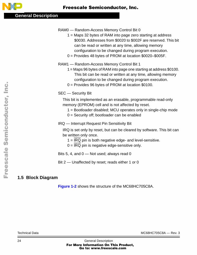
1.5 Block Diagram
Figure 1-2 shows the structure of the MC68HC705C8A.
Technical Data MC68HC705C8A — Rev. 3
24 General Description For More Information On This Product,
Go to: www.freescale.com

General DescriptionBlock Diagram
F
ree
sca
le S
em
ico
nd
uc
tor,
I
Freescale Semiconductor, Inc.n
c..
.
Figure 1-2. MC68HC705C8A Block Diagram
INTERNALPROCESSOR
CLOCK
TCAP
÷ 2
ACCUMULATOR
INDEX REGISTER
OSC1
OSC2OSCILLATOR
IRQ
RESET
COP WATCHDOG
CPU
M68HC05 CPU
ARITHMETIC
VDD
VSS
CPU REGISTERS
CONTROL
POR
T A
DAT
A D
IREC
TIO
N A
PA0
PA1
PA2
PA3
PA4
PA5
PA6
PA7
POWER
OPTION
EPROM/OTPROM — 7744 BYTES
1100000
CZNIH111
16-BITCAPTURE/COMPARE
POR
T B
DATA
DIR
ECTI
ON
B
PB0*PB1*PB2*PB3*PB4*PB5*PB6*PB7*
POR
T C
DAT
A D
IREC
TIO
N C
PC0
PC1
PC2
PC3
PC4
PC5
PC6
PC7†
TIMER SYSTEM
BAUD RATEGENERATOR
PD7
RDI (PD0)
TDO (PD1)
MISO (PD2)
MOSI (PD3)
SCK (PD4)
SS (PD5)
SCI
SPI
TCMP
RAM — 176 BYTES
REGISTER
BOOT ROM — 240 BYTES
(144 BYTES CONFIGURABLE)
PROGRAM REGISTEREPROM PROGRAMMINGVPP
ANDCLOCK MONITOR
POR
T D
LOGIC UNIT
(304 BYTES MAXIMUM)
CONTROL
PROGRAM COUNTER
STACK POINTER
CONDITION CODE REGISTER
* Port B pins also function as external interrupts.† PC7 has a high current sink and source capability.
MC68HC705C8A — Rev. 3 Technical Data
MOTOROLA General Description For More Information On This Product,
Go to: www.freescale.com

General Description
F
ree
sca
le S
em
ico
nd
uc
tor,
I
Freescale Semiconductor, Inc.n
c..
.
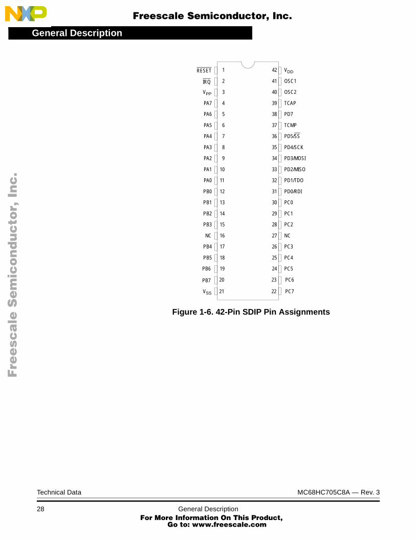
1.6 Pin Assignments
The MC68HC705C8A is available in six packages:
• 40-pin plastic dual in-line package (PDIP)
• 40-pin ceramic dual in-line package (cerdip)
• 44-lead plastic-leaded chip carrier (PLCC)
• 44-lead ceramic-leaded chip carrier (CLCC)
• 44-pin quad flat pack (QFP)
• 42-pin shrink dual in-line package (SDIP)
The pin assignments for these packages are shown in Figure 1-3, Figure 1-4, Figure 1-5, and Figure 1-6.
Figure 1-3. 40-Pin PDIP/Cerdip Pin Assignments
1
2
3
4
5
6
7
8
9
10
11
12
13
14 27
28
29
30
31
32
33
34
35
36
37
38
39
40 VDD
OSC1
OSC2
TCAP
PD7
TCMP
PD5/SS
PD4/SCK
PD3/MOSI
PD2/MISO
PD1/TDO
PD0/RDI
PC0
PC1
RESET
IRQ
VPP
PA7
PA5
PA4
PA3
PA2
PA1
PA0
PB0
PB1
PB2
PA6
15
16
17
18
19
20
PB4
PB5
PB6
PB7
VSS
PB3
21
22
23
24
25
26 PC2
PC3
PC4
PC5
PC6
PC7
Technical Data MC68HC705C8A — Rev. 3
26 General Description For More Information On This Product,
Go to: www.freescale.com

General DescriptionPin Assignments
F
ree
sca
le S
em
ico
nd
uc
tor,
I
Freescale Semiconductor, Inc.n
c..
.
Figure 1-4. 44-Lead PLCC/CLCC Pin Assignments
Figure 1-5. 44-Pin QFP Pin Assignments
PA6
PA7
V PP
NC IRQ
RESE
T
V DD
OSC
1
OSC
2
TCAP
NC
6 5 4 3 2 1 44 43 42 41 40
39
38
37
PD7TCMPPD5/SS
36
35
PD4/SCK
PD3/MOSI
34 PD2/MISO
33 PD1/TDO
32 PD0/RDI
31 PC0
30 PC1
29 PC2
2827262524232221201918N
C
PB5
PB6
PB7
V SS
NC
PC7
PC6
PC5
PC4
PC3
PB4
PB3
PB2PB1
17
16
15
14PB0
PA0
PA1
PA2
13
12
11
10
PA3 9
PA4 8PA5 7
PD7
TCAP
OSC2
OSC1
VDD
NC
NC
RESET
IRQ
VPP
PA7
PA6
PA5
PA4
PA3
PA2
PA1
PA0
PB0
PB1
PB2
PB3
PD3/
MO
SI
PD2/
MIS
O
PD4/
SCK
PD5/
SS
TCM
P
PD1/T
DO
PD0/
RDI
PC0
PC1
PC2
PC3
NC
PC4
PC5
PC6
PC7
VSS
NC
PB7
PB6
PB5
PB412 3 4 5 6 7 8 9 10 11
12
13
14
15
16
17
18
19
20
21
222324252627282930313233
34
35
36
37
38
39
40
41
42
4344
MC68HC705C8A — Rev. 3 Technical Data
MOTOROLA General Description For More Information On This Product,
Go to: www.freescale.com
General Description
F
ree
sca
le S
em
ico
nd
uc
tor,
I
Freescale Semiconductor, Inc.n
c..
.
Figure 1-6. 42-Pin SDIP Pin Assignments
VPP
PA7
PA6
PA5
PA4
PA3
PA2
PA1
PA0
PB0
PB1
PB2
PB3
NC
PB4
PB5
PB6
VSS
VDD
OSC1
OSC2
TCAP
PD7
TCMP
PD5/SS
PD4/SCK
PD3/MOSI
PD2/MISO
PD1/TDO
PD0/RDI
PC0
PC1
PC2
NC
PC3
PC4
PC5
PC6
1
2
3
4
5
6
7
8
9
10
11
12
13
14
15
16
17
18
19
20
42
41
40
39
38
37
36
35
34
33
32
31
30
29
28
27
26
25
24
23
22 PC7
PB7
21
RESET
IRQ
Technical Data MC68HC705C8A — Rev. 3
28 General Description For More Information On This Product,
Go to: www.freescale.com

General DescriptionPin Functions
F
ree
sca
le S
em
ico
nd
uc
tor,
I
Freescale Semiconductor, Inc.n
c..
.
1.7 Pin Functions
This subsection describes the MC68HC705C8A signals. Reference is made, where applicable, to other sections that contain more detail about the function being performed.
1.7.1 VDD and VSS
VDD and VSS are the power supply and ground pins. The MCU operates from a single power supply.
Very fast signal transitions occur on the MCU pins, placing high short-duration current demands on the power supply. To prevent noise problems, take special care to provide good power supply bypassing at the MCU. Place bypass capacitors as close to the MCU as possible, as shown in Figure 1-7.
1.7.2 VPP
This pin provides the programming voltage to the EPROM array. For normal operation, VPP shuld be tied to VDD.
NOTE: Connecting the VPP pin (programming voltage) to VSS (ground) could result in damage to the MCU.
MCU C2
VDD
VSS
V+
+C1
Figure 1-7. Bypassing Layout Recommendation
MC68HC705C8A — Rev. 3 Technical Data
MOTOROLA General Description For More Information On This Product,
Go to: www.freescale.com

General Description
F
ree
sca
le S
em
ico
nd
uc
tor,
I
Freescale Semiconductor, Inc.n
c..
.
1.7.3 OSC1 and OSC2
The OSC1 and OSC2 pins are the control connections for the 2-pin on-chip oscillator. The oscillator can be driven by:
• Crystal resonator
• Ceramic resonator
• External clock signal
NOTE: The frequency of the internal oscillator is fOSC. The MCU divides the internal oscillator output by two to produce the internal clock with a frequency of fOP.
1.7.3.1 Crystal Resonator
The circuit in Figure 1-8 shows a crystal oscillator circuit for an AT-cut, parallel resonant crystal. Follow the crystal supplier’s recommendations, because the crystal parameters determine the external component values required to provide reliable startup and maximum stability. The load capacitance values used in the oscillator circuit design should account for all stray layout capacitances. To minimize output distortion, mount the crystal and capacitors as close as possible to the pins.
NOTE: Use an AT-cut crystal and not a strip or tuning fork crystal. The MCU might overdrive or have the incorrect characteristic impedance for a strip or tuning fork crystal.
MCU
OSC1 OSC2
XTAL22 pF∗ 22 pF∗
10 MΩ∗
2 MHz
Figure 1-8. Crystal Connections
∗ Starting value only. Follow crystal supplier’srecommendations regarding component values that will provide reliable startup and maximum stability.
Technical Data MC68HC705C8A — Rev. 3
30 General Description For More Information On This Product,
Go to: www.freescale.com

General DescriptionPin Functions
F
ree
sca
le S
em
ico
nd
uc
tor,
I
Freescale Semiconductor, Inc.n
c..
.
1.7.3.2 Ceramic Resonator
To reduce cost, use a ceramic resonator instead of a crystal. Use the circuit shown in Figure 1-9 for a 2-pin ceramic resonator or the circuit shown in Figure 1-10 for a 3-pin ceramic resonator, and follow the resonator manufacturer’s recommendations.
The external component values required for maximum stability and reliable starting depend upon the resonator parameters. The load capacitance values used in the oscillator circuit design should include all stray layout capacitances. To minimize output distortion, mount the resonator and capacitors as close as possible to the pins.
NOTE: The bus frequency (fOP) is one-half the external or crystal frequency (fOSC), while the processor clock cycle (tCYC) is two times the fOSC period.
MCU
OSC1 OSC2
CERAMICC C
R
RESONATOR
Figure 1-9. 2-Pin Ceramic Resonator Connections
.
MCU
OSC1 OSC2
CERAMICRESONATOR
Figure 1-10. 3-Pin Ceramic Resonator
Connections
MC68HC705C8A — Rev. 3 Technical Data
MOTOROLA General Description For More Information On This Product,
Go to: www.freescale.com
General Description
F
ree
sca
le S
em
ico
nd
uc
tor,
I
Freescale Semiconductor, Inc.n
c..
.
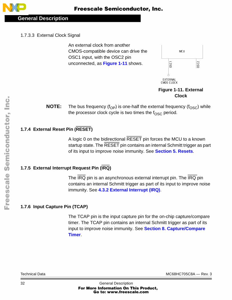
1.7.3.3 External Clock Signal
An external clock from another CMOS-compatible device can drive the OSC1 input, with the OSC2 pin unconnected, as Figure 1-11 shows.
NOTE: The bus frequency (fOP) is one-half the external frequency (fOSC) while the processor clock cycle is two times the fOSC period.
1.7.4 External Reset Pin (RESET)
A logic 0 on the bidirectional RESET pin forces the MCU to a known startup state. The RESET pin contains an internal Schmitt trigger as part of its input to improve noise immunity. See Section 5. Resets.
1.7.5 External Interrupt Request Pin (IRQ)
The IRQ pin is an asynchronous external interrupt pin. The IRQ pin contains an internal Schmitt trigger as part of its input to improve noise immunity. See 4.3.2 External Interrupt (IRQ).
1.7.6 Input Capture Pin (TCAP)
The TCAP pin is the input capture pin for the on-chip capture/compare timer. The TCAP pin contains an internal Schmitt trigger as part of its input to improve noise immunity. See Section 8. Capture/Compare Timer.
MCU
OSC
1
OSC
2
EXTERNALCMOS CLOCK
Figure 1-11. External Clock
Technical Data MC68HC705C8A — Rev. 3
32 General Description For More Information On This Product,
Go to: www.freescale.com

General DescriptionPin Functions
F
ree
sca
le S
em
ico
nd
uc
tor,
I
Freescale Semiconductor, Inc.n
c..
.
1.7.7 Output Compare Pin (TCMP)
The TCMP pin is the output compare pin for the on-chip capture/compare timer. See Section 8. Capture/Compare Timer.
1.7.8 Port A I/O Pins (PA7–PA0)
These eight I/O lines comprise port A, a general-purpose, bidirectional I/O port. The pins are programmable as either inputs or outputs under software control of the data direction registers. See 7.3 Port A.
1.7.9 Port B I/O Pins (PB7–PB0)
These eight I/O pins comprise port B, a general-purpose, bidirectional I/O port. The pins are programmable as either inputs or outputs under software control of the data direction registers. Port B pins also can be configured to function as external interrupts. See 7.4 Port B.
1.7.10 Port C I/O Pins (PC7–PC0)
These eight I/O pins comprise port C, a general-purpose, bidirectional I/O port. The pins are programmable as either inputs or outputs under software control of the data direction registers. PC7 has a high current sink and source capability. See 7.5 Port C.
1.7.11 Port D I/O Pins (PD7 and PD5–PD0)
These seven lines comprise port D, a fixed input port. All special functions that are enabled (SPI and SCI) affect this port. See 7.6 Port D.
MC68HC705C8A — Rev. 3 Technical Data
MOTOROLA General Description For More Information On This Product,
Go to: www.freescale.com

General Description
F
ree
sca
le S
em
ico
nd
uc
tor,
I
Freescale Semiconductor, Inc.n
c..
.
Technical Data MC68HC705C8A — Rev. 3
34 General Description For More Information On This Product,
Go to: www.freescale.com
F
ree
sca
le S
em
ico
nd
uc
tor,
IFreescale Semiconductor, Inc.
nc
...
Technical Data — MC68HC705C8A
Section 2. Memory
2.1 Contents
2.2 Introduction . . . . . . . . . . . . . . . . . . . . . . . . . . . . . . . . . . . . . . . .35
2.3 Memory Map. . . . . . . . . . . . . . . . . . . . . . . . . . . . . . . . . . . . . . .35
2.4 Input/Output (I/O) . . . . . . . . . . . . . . . . . . . . . . . . . . . . . . . . . . .36
2.5 RAM . . . . . . . . . . . . . . . . . . . . . . . . . . . . . . . . . . . . . . . . . . . . .36
2.6 EPROM/OTPROM (PROM) . . . . . . . . . . . . . . . . . . . . . . . . . . .37
2.7 Bootloader ROM. . . . . . . . . . . . . . . . . . . . . . . . . . . . . . . . . . . .37
2.2 Introduction
This section describes the organization of the on-chip memory.
2.3 Memory Map
The central processor unit (CPU) can address eight Kbytes of memory and input/output (I/O) registers. The program counter typically advances one address at a time through memory, reading the program instructions and data. The programmable read-only memory (PROM) portion of memory — either one-time programmable read-only memory (OTPROM) or erasable, programmable read-only memory (EPROM) — holds the program instructions, fixed data, user-defined vectors, and interrupt service routines. The random-access memory (RAM) portion of memory holds variable data.
I/O registers are memory-mapped so that the CPU can access their locations in the same way that it accesses all other memory locations. The shared stack area is used during processing of an interrupt or
MC68HC705C8A — Rev. 3 Technical Data
MOTOROLA Memory For More Information On This Product,
Go to: www.freescale.com

Memory
F
ree
sca
le S
em
ico
nd
uc
tor,
I
Freescale Semiconductor, Inc.n
c..
.
subroutine call to save the CPU state. The stack pointer decrements during pushes and increments during pulls.
Figure 2-1 is a memory map of the MCU. Addresses $0000–$001F, shown in Figure 2-2, contain most of the control, status, and data registers. Additional I/O registers have these addresses:
• $1FDF, option register
• $1FF0, mask option register 1 (MOR1)
• $1FF1, mask option register 2 (MOR2)
2.4 Input/Output (I/O)
The first 32 addresses of memory space, from $0000 to $001F, are the I/O section. These are the addresses of the I/O control registers, status registers, and data registers. See Figure 2-2 for more information.
2.5 RAM
One of four selectable memory configurations is selected by the state of the RAM1 and RAM0 bits in the option register located at $1FDF. Reset or power-on reset (POR) clears these bits, automatically selecting the first memory configuration as shown in Table 2-1. See 9.5.1 Option Register.
NOTE: Be careful when using nested subroutines or multiple interrupt levels. The CPU can overwrite data in the stack RAM during a subroutine or during the interrupt stacking operation.
Table 2-1. Memory Configurations
RAM0 RAM1 RAM Bytes PROM Bytes
0 0 176 7744
1 0 208 7696
0 1 272 7648
1 1 304 7600
Technical Data MC68HC705C8A — Rev. 3
36 Memory For More Information On This Product,
Go to: www.freescale.com

MemoryEPROM/OTPROM (PROM)
F
ree
sca
le S
em
ico
nd
uc
tor,
I
Freescale Semiconductor, Inc.n
c..
.
2.6 EPROM/OTPROM (PROM)
An MCU with a quartz window has a maximum of 7744 bytes of EPROM. The quartz window allows the EPROM erasure with ultraviolet light. In an MCU without a quartz window, the EPROM cannot be erased and serves a maximum 7744 bytes of OTPROM (see Table 2-1). See Section 9. EPROM/OTPROM (PROM).
2.7 Bootloader ROM
The 240 bytes at addresses $1F00–$1FEF are reserved ROM addresses that contain the instructions for the bootloader functions. See Section 9. EPROM/OTPROM (PROM).
MC68HC705C8A — Rev. 3 Technical Data
MOTOROLA Memory For More Information On This Product,
Go to: www.freescale.com

Memory
F
ree
sca
le S
em
ico
nd
uc
tor,
I
Freescale Semiconductor, Inc.n
c..
.
Figure 2-1. Memory Map
$0000I/O REGISTERS
32 BYTES
PORT A DATA REGISTER $0000PORT B DATA REGISTER $0001
$001F PORT C DATA REGISTER $0002$0020
UNUSED16 BYTES
USER PROM48 BYTES
PORT D FIXED INPUT PORT $0003PORT A DATA DIRECTION REGISTER $0004
$002F PORT B DATA DIRECTION REGISTER $0005$0030
RAM32 BYTES
PORT C DATA DIRECTION REGISTER $0006UNUSED $0007UNUSED $0008
$004F RAM0 = 1(1) RAM0 = 0(1) UNUSED $0009$0050 SPI CONTROL REGISTER $000A
SPI STATUS REGISTER $000B$00BF SPI DATA REGISTER $000C$00C0
STACK64 BYTES
SCI BAUD RATE REGISTER $000DSCI CONTROL REGISTER 1 $000E
$00FF SCI CONTROL REGISTER 2 $000F$0100
USER PROM96 BYTES
RAM96 BYTES
SCI STATUS REGISTER $0010SCI DATA REGISTER $0011
TIMER CONTROL REGISTER $0012TIMER STATUS REGISTER $0013
INPUT CAPTURE REGISTER (HIGH) $0014INPUT CAPTURE REGISTER (LOW) $0015
OUTPUT COMPARE REGISTER (HIGH) $0016OUTPUT COMPARE REGISTER (LOW) $0017
$015F RAM1 = 0(1) RAM1 = 1(1) TIMER REGISTER (HIGH) $0018$0160
USER PROM7584 BYTES
TIMER REGISTER (LOW) $0019ALTERNATE TIMER REGISTER (HIGH) $001A
$1EFF ALTERNATE TIMER REGISTER (LOW) $001B$1F00
BOOTLOADER ROM240 BYTES
EPROM PROGRAM REGISTER $001CCOP RESET REGISTER $001D
$1FDE COP CONTROL REGISTER $001E$1FDF OPTION REGISTER UNUSED $001F$1FE0
$1FEF
BOOT ROM VECTORS16 BYTES
$1FF0 MASK OPTION REGISTER 1RESERVED $1FF2RESERVED $1FF3
$1FF1 MASK OPTION REGISTER 2SPI INTERRUPT VECTOR (HIGH) $1FF4SPI INTERRUPT VECTOR (LOW) $1FF5
$1FF2USER PROM VECTORS
12 BYTES
SCI INTERRUPT VECTOR (HIGH) $1FF6SCI INTERRUPT VECTOR (LOW) $1FF7
$1FFF TIMER INTERRUPT VECTOR (HIGH) $1FF8TIMER INTERRUPT VECTOR (LOW) $1FF9
EXTERNAL INTERRUPT VECTOR (HIGH) $1FFA(1) See 9.5.1 Option Register for information. EXTERNAL INTERRUPT VECTOR (LOW) $1FFB
SOFTWARE INTERRUPT VECTOR (HIGH) $1FFCSOFTWARE INTERRUPT VECTOR (LOW) $1FFD
RESET VECTOR (HIGH) $1FFERESET VECTOR (LOW) $1FFF
RAM176 BYTES
Technical Data MC68HC705C8A — Rev. 3
38 Memory For More Information On This Product,
Go to: www.freescale.com

MemoryBootloader ROM
F
ree
sca
le S
em
ico
nd
uc
tor,
I
Freescale Semiconductor, Inc.n
c..
.
Addr. Register Name Bit 7 6 5 4 3 2 1 Bit 0
$0000Port A Data Register
(PORTA)See page 78.
Read:PA7 PA6 PA5 PA4 PA3 PA2 PA1 PA0
Write:
Reset: Unaffected by reset
$0001Port B Data Register
(PORTB)See page 81.
Read:PB7 PB6 PB5 PB4 PB3 PB2 PB1 PB0
Write:
Reset: Unaffected by reset
$0002Port C Data Register
(PORTC)See page 85.
Read:PC7 PC6 PC5 PC4 PC3 PC2 PC1 PC0
Write:
Reset: Unaffected by reset
$0003Port D Fixed Input Register
(PORTD)See page 88.
Read: PD7 SS SCK MOSI MISO TDO RDI
Write:
Reset: Unaffected by reset
$0004Port A Data Direction
Register (DDRA)See page 79.
Read:DDRA7 DDRA6 DDRA5 DDRA4 DDRA3 DDRA2 DDRA1 DDRA0
Write:
Reset: 0 0 0 0 0 0 0 0
$0005Port B Data Direction
Register (DDRB)See page 82.
Read:DDRB7 DDRB6 DDRB5 DDRB4 DDRB3 DDRB2 DDRB1 DDRB0
Write:
Reset: 0 0 0 0 0 0 0 0
$0006Port C Data Direction
(DDRC)See page 86.
Read:DDRC7 DDRC6 DDRC5 DDRC4 DDRC3 DDRC2 DDRC1 DDRC0
Write:
Reset: 0 0 0 0 0 0 0 0
$0007 Unimplemented
$0008 Unimplemented
$0009 Unimplemented
= Unimplemented U = Unaffected
Figure 2-2. I/O Register Summary (Sheet 1 of 4)
MC68HC705C8A — Rev. 3 Technical Data
MOTOROLA Memory For More Information On This Product,
Go to: www.freescale.com

Memory
F
ree
sca
le S
em
ico
nd
uc
tor,
I
Freescale Semiconductor, Inc.n
c..
.
$000ASPI Control Register
(SPCR)See page 149.
Read:SPIE SPE MSTR CPOL CPHA SPR1 SPR0
Write:
Reset: 0 0 0 U U U U
$000BSPI Status Register
(SPSR)See page 151.
Read: SPIF WCOL MODF
Write:
Reset: 0 0 0
$000CSPI Data Register
(SPDR)See page 149.
Read:Bit 7 Bit 6 Bit 5 Bit 4 Bit 3 BIt 2 Bit 1 Bit 0
Write:
Reset: Unaffected by reset
$000DBaud Rate Register
(Baud)See page 136.
Read:SCP1 SCP0 SCR2 SCR1 SCR0
Write:
Reset: U U 0 0 U U U U
$000ESCI Control Register 1
(SCCR1)See page 130.
Read:R8 T8 M WAKE
Write:
Reset: U U U U
$000FSCI Control Register 2
(SCCR2)See page 131.
Read:TIE TCIE RIE ILIE TE RE RWU SBK
Write:
Reset: 0 0 0 0 0 0 0 0
$0010SCI Status Register
(SCSR)See page 133.
Read: TDRE TC RDRF IDLE OR NF FE
Write:
Reset: 1 1 0 0 0 0 0 U
$0011SCI Data Register
(SCDR)See page 129.
Read:Bit 7 Bit 6 Bit 5 Bit 4 Bit 3 Bit 2 Bit 1 Bit 0
Write:
Reset: Unaffected by reset
$0012Timer Control Register
(TCR)See page 94.
Read:ICIE OCIE TOIE 0 0 0 IEDG OLVL
Write:
Reset: 0 0 0 0 0 0 U 0
Addr. Register Name Bit 7 6 5 4 3 2 1 Bit 0
= Unimplemented U = Unaffected
Figure 2-2. I/O Register Summary (Sheet 2 of 4)
Technical Data MC68HC705C8A — Rev. 3
40 Memory For More Information On This Product,
Go to: www.freescale.com

MemoryBootloader ROM
F
ree
sca
le S
em
ico
nd
uc
tor,
I
Freescale Semiconductor, Inc.n
c..
.
$0013Timer Status Register
(TSR)See page 96.
Read: ICF OCF TOF 0 0 0 0 0
Write:
Reset: U U U 0 0 0 0 0
$0014Input Capture Register
High (ICRH)See page 100.
Read: Bit 15 Bit 14 Bit 13 Bit 12 Bit 11 Bit 10 Bit 9 Bit 8
Write:
Reset: Unaffected by reset
$0015Input Capture Register
Low (ICRL)See page 100.
Read: Bit 7 Bit 6 Bit 5 Bit 4 Bit 3 Bit 2 Bit 1 Bit 0
Write:
Reset: Unaffected by reset
$0016
Output Compare RegisterHigh (OCRH)
See page 101.
Read:Bit 15 Bit 14 Bit 13 Bit 12 Bit 11 Bit 10 Bit 9 Bit 8
Write:
Reset: Unaffected by reset
$0017Output Compare Register
Low (OCRL)See page 101.
Read:Bit 7 Bit 6 Bit 5 Bit 4 Bit 3 Bit 2 Bit 1 Bit 0
Write:
Reset: Unaffected by reset
$0018Timer Register High
(TRH)See page 97.
Read: Bit 15 Bit 14 Bit 13 Bit 12 Bit 11 Bit 10 Bit 9 Bit 8
Write:
Reset: Reset initializes TRH to $FF
$0019Timer Register Low
(TRL)See page 97.
Read: Bit 7 Bit 6 Bit 5 Bit 4 Bit 3 Bit 2 Bit 1 Bit 0
Write:
Reset: Reset initializes TRL to $FC
$001AAlternate Timer Register
High (ATRH)See page 99.
Read: Bit 15 Bit 14 Bit 13 Bit 12 Bit 11 Bit 10 Bit 9 Bit 8
Write:
Reset: Reset initializes ATRH to $FF
$001BAlternate Timer Register
Low (ATRL)See page 99.
Read: Bit 7 Bit 6 Bit 5 Bit 4 Bit 3 Bit 2 Bit 1 Bit 0
Write:
Reset: Reset initializes ATRL to $FC
Addr. Register Name Bit 7 6 5 4 3 2 1 Bit 0
= Unimplemented U = Unaffected
Figure 2-2. I/O Register Summary (Sheet 3 of 4)
MC68HC705C8A — Rev. 3 Technical Data
MOTOROLA Memory For More Information On This Product,
Go to: www.freescale.com

Memory
F
ree
sca
le S
em
ico
nd
uc
tor,
I
Freescale Semiconductor, Inc.n
c..
.
$001CEPROM Programming
Register (PROG)See page 109.
Read:0 0 0 0 0 LAT 0 PGM
Write:
Reset: 0 0 0 0 0 0 0 0
$001DProgrammable COP Reset
Register (COPRST)See page 64.
Read:
Write: Bit 7 Bit 6 Bit 5 Bit 4 Bit 3 Bit 2 Bit 1 Bit 0
Reset: U U U U U U U U
$001EProgrammable COP Control
Register (COPCR)See page 64.
Read: 0 0 0 COPFCME PCOPE CM1 CM0
Write:
Reset: 0 0 0 U 0 0 0 0
$001F Unimplemented
$1FDFOption Register
(Option)See page 116.
Read:RAM0 RAM1 0 0 SEC* IRQ 0
Write:
Reset: 0 0 0 0 * U 1 0
*Implemented as an EPROM cell
$1FF0Mask Option Register 1
(MOR1)See page 117.
Read:PBPU7 PBPU6 PBPU5 PBPU4 PBPU3 PBPU2 PBPU1
PBPU0/COPCWrite:
Reset: Unaffected by reset
$1FF1Mask Option Register 2
(MOR2)See page 118.
Read:NCOPE
Write:
Reset: Unaffected by reset
Addr. Register Name Bit 7 6 5 4 3 2 1 Bit 0
= Unimplemented U = Unaffected
Figure 2-2. I/O Register Summary (Sheet 4 of 4)
Technical Data MC68HC705C8A — Rev. 3
42 Memory For More Information On This Product,
Go to: www.freescale.com

F
ree
sca
le S
em
ico
nd
uc
tor,
IFreescale Semiconductor, Inc.
nc
...
Technical Data — MC68HC705C8A
Section 3. Central Processor Unit (CPU)
3.1 Contents
3.2 Introduction . . . . . . . . . . . . . . . . . . . . . . . . . . . . . . . . . . . . . . . .43
3.3 CPU Registers . . . . . . . . . . . . . . . . . . . . . . . . . . . . . . . . . . . . .443.3.1 Accumulator . . . . . . . . . . . . . . . . . . . . . . . . . . . . . . . . . . . .453.3.2 Index Register . . . . . . . . . . . . . . . . . . . . . . . . . . . . . . . . . . .453.3.3 Stack Pointer . . . . . . . . . . . . . . . . . . . . . . . . . . . . . . . . . . . .463.3.4 Program Counter . . . . . . . . . . . . . . . . . . . . . . . . . . . . . . . . .463.3.5 Condition Code Register . . . . . . . . . . . . . . . . . . . . . . . . . . .47
3.4 Arithmetic/Logic Unit (ALU) . . . . . . . . . . . . . . . . . . . . . . . . . . .48
3.2 Introduction
This section describes the central processor unit (CPU) registers.
MC68HC705C8A — Rev. 3 Technical Data
MOTOROLA Central Processor Unit (CPU) For More Information On This Product,
Go to: www.freescale.com

Central Processor Unit (CPU)
F
ree
sca
le S
em
ico
nd
uc
tor,
I
Freescale Semiconductor, Inc.n
c..
.
3.3 CPU Registers
Figure 3-1 shows the five CPU registers. These are hard-wired registers within the CPU and are not part of the memory map.
Figure 3-1. Programming Model
ACCUMULATOR (A)
INDEX REGISTER (X)
1 10 00 0 0
Z CI N1 H1 1
Bit 04Bit 7 5
CONDITION CODE REGISTER (CCR)
PROGRAM COUNTER (PC)
STACK POINTER (SP)
HALF-CARRY FLAG
INTERRUPT MASK
NEGATIVE FLAG
ZERO FLAG
CARRY/BORROW FLAG
6 3 2 1
Bit 047 56 3 2 1
Bit 047 56 3 2 1
Bit 04Bit 7 56 3 2 1
Bit 04Bit 7 56 3 2 1
8Bit 12 11 10 9
8Bit 12 11 10 9
Technical Data MC68HC705C8A — Rev. 3
44 Central Processor Unit (CPU) For More Information On This Product,
Go to: www.freescale.com

Central Processor Unit (CPU)CPU Registers
F
ree
sca
le S
em
ico
nd
uc
tor,
I
Freescale Semiconductor, Inc.n
c..
.
3.3.1 Accumulator
The accumulator (A) shown in Figure 3-2 is a general-purpose 8-bit register. The CPU uses the accumulator to hold operands and results of arithmetic and non-arithmetic operations.
Figure 3-2. Accumulator (A)
3.3.2 Index Register
In the indexed addressing modes, the CPU uses the byte in the index register (X) shown in Figure 3-3 to determine the conditional address of the operand. See 12.3.5 Indexed, No Offset, 12.3.6 Indexed, 8-Bit Offset, and 12.3.7 Indexed, 16-Bit Offset for more information on indexed addressing.
The 8-bit index register also can serve as a temporary data storage location.
Figure 3-3. Index Register (X)
Bit 7 6 5 4 3 2 1 Bit 0
Read:
Write:
Reset: Unaffected by reset
Bit 7 6 5 4 3 2 1 Bit 0
Read:
Write:
Reset: Unaffected by reset
MC68HC705C8A — Rev. 3 Technical Data
MOTOROLA Central Processor Unit (CPU) For More Information On This Product,
Go to: www.freescale.com
Central Processor Unit (CPU)
F
ree
sca
le S
em
ico
nd
uc
tor,
I
Freescale Semiconductor, Inc.n
c..
.
3.3.3 Stack Pointer
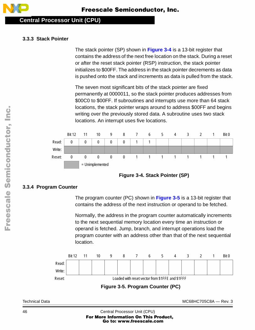
The stack pointer (SP) shown in Figure 3-4 is a 13-bit register that contains the address of the next free location on the stack. During a reset or after the reset stack pointer (RSP) instruction, the stack pointer initializes to $00FF. The address in the stack pointer decrements as data is pushed onto the stack and increments as data is pulled from the stack.
The seven most significant bits of the stack pointer are fixed permanently at 0000011, so the stack pointer produces addresses from $00C0 to $00FF. If subroutines and interrupts use more than 64 stack locations, the stack pointer wraps around to address $00FF and begins writing over the previously stored data. A subroutine uses two stack locations. An interrupt uses five locations.
Figure 3-4. Stack Pointer (SP)
3.3.4 Program Counter
The program counter (PC) shown in Figure 3-5 is a 13-bit register that contains the address of the next instruction or operand to be fetched.
Normally, the address in the program counter automatically increments to the next sequential memory location every time an instruction or operand is fetched. Jump, branch, and interrupt operations load the program counter with an address other than that of the next sequential location.
Bit 12 11 10 9 8 7 6 5 4 3 2 1 Bit 0
Read: 0 0 0 0 0 1 1
Write:
Reset: 0 0 0 0 0 1 1 1 1 1 1 1 1
= Unimplemented
Bit 12 11 10 9 8 7 6 5 4 3 2 1 Bit 0
Read:
Write:
Reset: Loaded with reset vector from $1FFE and $1FFF
Figure 3-5. Program Counter (PC)
Technical Data MC68HC705C8A — Rev. 3
46 Central Processor Unit (CPU) For More Information On This Product,
Go to: www.freescale.com

Central Processor Unit (CPU)CPU Registers
F
ree
sca
le S
em
ico
nd
uc
tor,
I
Freescale Semiconductor, Inc.n
c..
.
3.3.5 Condition Code Register
The condition code register (CCR) shown in Figure 3-6 is an 8-bit register whose three most significant bits are permanently fixed at 111. The condition code register contains the interrupt mask and four bits that indicate the results of prior instructions.
H — Half-Carry Bit
The CPU sets the half-carry flag when a carry occurs between bits 3 and 4 of the accumulator during an add without carry (ADD) or add with carry (ADC) operation. The half-carry bit is required for binary-coded decimal (BCD) arithmetic operations. Reset has no affect on the half-carry flag.
I — Interrupt Mask Bit
Setting the interrupt mask (I) disables interrupts. If an interrupt request occurs while the interrupt mask is a logic 0, the CPU saves the CPU registers on the stack, sets the interrupt mask, and then fetches the interrupt vector. If an interrupt request occurs while the interrupt mask is set, the interrupt request is latched. The CPU processes the latched interrupt as soon as the interrupt mask is cleared again.
A return-from-interrupt (RTI) instruction pulls the CPU registers from the stack, restoring the interrupt mask to its cleared state. After a reset, the interrupt mask is set and can be cleared only by a CLI, STOP, or WAIT instruction.
Bit 7 6 5 4 3 2 1 Bit 0
Read: 1 1 1H I N Z C
Write:
Reset: 1 1 1 U 1 U U U
= Unimplemented U = Unaffected
Figure 3-6. Condition Code Register (CCR)
MC68HC705C8A — Rev. 3 Technical Data
MOTOROLA Central Processor Unit (CPU) For More Information On This Product,
Go to: www.freescale.com

Central Processor Unit (CPU)
F
ree
sca
le S
em
ico
nd
uc
tor,
I
Freescale Semiconductor, Inc.n
c..
.
N — Negative Flag
The CPU sets the negative flag when an arithmetic operation, logical operation, or data manipulation produces a negative result (bit 7 in the results is a logic 1). Reset has no effect on the negative flag.
Z — Zero Flag
The CPU sets the zero flag when an arithmetic operation, logical operation, or data manipulation produces a result of $00. Reset has no effect on the zero flag.
C — Carry/Borrow Flag
The CPU sets the carry/borrow flag when an addition operation produces a carry out of bit 7 of the accumulator or when a subtraction operation requires a borrow. Some logical operations and data manipulation instructions also clear or set the carry/borrow bit. Reset has no effect on the carry/borrow flag.
3.4 Arithmetic/Logic Unit (ALU)
The arithmetic/logic unit (ALU) performs the arithmetic and logical operations defined by the instruction set. The binary arithmetic circuits decode instructions and set up the ALU for the selected operation. Most binary arithmetic is based on the addition algorithm, carrying out subtraction as negative addition. Multiplication is not performed as a discrete operation but as a chain of addition and shift operations within the ALU. The multiply instruction requires 11 internal clock cycles to complete this chain of operations.
Technical Data MC68HC705C8A — Rev. 3
48 Central Processor Unit (CPU) For More Information On This Product,
Go to: www.freescale.com
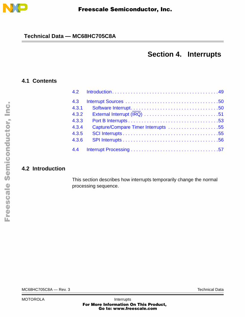
F
ree
sca
le S
em
ico
nd
uc
tor,
IFreescale Semiconductor, Inc.
nc
...
Technical Data — MC68HC705C8A
Section 4. Interrupts
4.1 Contents
4.2 Introduction . . . . . . . . . . . . . . . . . . . . . . . . . . . . . . . . . . . . . . . .49
4.3 Interrupt Sources . . . . . . . . . . . . . . . . . . . . . . . . . . . . . . . . . . .504.3.1 Software Interrupt. . . . . . . . . . . . . . . . . . . . . . . . . . . . . . . . .504.3.2 External Interrupt (IRQ) . . . . . . . . . . . . . . . . . . . . . . . . . . . .514.3.3 Port B Interrupts . . . . . . . . . . . . . . . . . . . . . . . . . . . . . . . . . .534.3.4 Capture/Compare Timer Interrupts . . . . . . . . . . . . . . . . . . .554.3.5 SCI Interrupts . . . . . . . . . . . . . . . . . . . . . . . . . . . . . . . . . . . .554.3.6 SPI Interrupts . . . . . . . . . . . . . . . . . . . . . . . . . . . . . . . . . . . .56
4.4 Interrupt Processing . . . . . . . . . . . . . . . . . . . . . . . . . . . . . . . . .57
4.2 Introduction
This section describes how interrupts temporarily change the normal processing sequence.
MC68HC705C8A — Rev. 3 Technical Data
MOTOROLA Interrupts For More Information On This Product,
Go to: www.freescale.com

Interrupts
F
ree
sca
le S
em
ico
nd
uc
tor,
I
Freescale Semiconductor, Inc.n
c..
.
4.3 Interrupt Sources
These sources can generate interrupts:
• Software instructions (SWI)
• External interrupt pin (IRQ)
• Port B pins
• Serial communications interface (SCI):
– SCI transmit data register empty
– SCI transmission complete
– SCI receive data register full
– SCI receiver overrun
– SCI receiver input idle
• Serial peripheral interface (SPI):
– SPI transmission complete
– SPI mode fault
– SPI overrun
The IRQ pin, port B pins, SCI, and SPI can be masked (disabled) by setting the I bit of the condition code register (CCR). The software interrupt (SWI) instruction is non-maskable.
An interrupt temporarily changes the program sequence to process a particular event. An interrupt does not stop the execution of the instruction in progress but takes effect when the current instruction completes its execution. Interrupt processing automatically saves the central processor unit (CPU) registers on the stack and loads the program counter with a user-defined vector address.
4.3.1 Software Interrupt
The software interrupt instruction (SWI) causes a non-maskable interrupt.
Technical Data MC68HC705C8A — Rev. 3
50 Interrupts For More Information On This Product,
Go to: www.freescale.com
InterruptsInterrupt Sources
F
ree
sca
le S
em
ico
nd
uc
tor,
I
Freescale Semiconductor, Inc.n
c..
.
4.3.2 External Interrupt (IRQ)
An interrupt signal on the IRQ pin latches an external interrupt request. After completing the current instruction, the CPU tests these bits:
• IRQ latch
• I bit in the CCR
Setting the I bit in the CCR disables external interrupts.
If the IRQ latch is set and the I bit is clear, the CPU then begins the interrupt sequence. The CPU clears the IRQ latch while it fetches the interrupt vector, so that another external interrupt request can be latched during the interrupt service routine. As soon as the I bit is cleared during the return-from-interrupt (RTI) instruction, the CPU can recognize the new interrupt request. Figure 4-1 shows the logic for external interrupts.
Figure 4-1 shows an external interrupt functional diagram. Figure 4-2 shows an external interrupt timing diagram for the interrupt line. The timing diagram illustrates two treatments of the interrupt line to the processor.
1. Two single pulses on the interrupt line are spaced far enough apart to be serviced. The minimum time between pulses is a function of the length of the interrupt service.
Once a pulse occurs, the next pulse normally should not occur until an RTI occurs. This time (tILIL) is obtained by adding 19 instruction cycles to the total number of cycles needed to complete the service routine (not including the RTI instruction).
2. Many interrupt lines are “wire-ORed” to the IRQ line. If the interrupt line remains low after servicing an interrupt, then the CPU continues to recognize an interrupt.
NOTE: The internal interrupt latch is cleared in the first part of the interrupt service routine. Therefore, a new external interrupt pulse could be latched and serviced as soon as the I bit is cleared.
If the IRQ pin is not in use, connect it to the VDD pin.
MC68HC705C8A — Rev. 3 Technical Data
MOTOROLA Interrupts For More Information On This Product,
Go to: www.freescale.com

Interrupts
F
ree
sca
le S
em
ico
nd
uc
tor,
I
Freescale Semiconductor, Inc.n
c..
.
Figure 4-1. External Interrupt Internal Function Diagram
Figure 4-2. External Interrupt Timing
R
C
D Q
Q
VDD
EXTERNAL INTERRUPT REQUEST
I BIT (CCR)
INTERNAL RESET (COP)
EXTERNAL RESET
EXTERNAL INTERRUPT BEING SERVICED(VECTOR FETCH)
EDGE- AND LEVEL-SENSITIVE TRIGGER
OPTION REGISTER
INTERRUPT PIN
IRQ LATCH
POR
NORMALLYUSED WITHWIRED-OR
CONNECTION
IRQ
tILIH
tILIL
tILIH
IRQ PIN
IRQ1
IRQn
.
.
.
a. Edge-Sensitive Trigger Condition. The minimum pulse width (tILIH) is either 125 ns (fOP = 2.1 MHz)or 250 ns (fOP = 1 MHz). The period tILIL should not be less than the number of tCYC cycles it takes toexecute the interrupt service routine plus 19 tCYC cycles.
b. Level-Sensitive Trigger Condition. If the interrupt line remains low after servicing an interrupt, then the CPU continues to recognize an interrupt.
(INTERNAL)
Technical Data MC68HC705C8A — Rev. 3
52 Interrupts For More Information On This Product,
Go to: www.freescale.com

InterruptsInterrupt Sources
F
ree
sca
le S
em
ico
nd
uc
tor,
I
Freescale Semiconductor, Inc.n
c..
.
4.3.3 Port B Interrupts
When these three conditions are true, a port B pin (PBx) acts as an external interrupt pin:
• The corresponding port B pullup bit (PBPUx) in mask option register 1 (MOR1) is programmed to a logic 1.
• The corresponding port B data direction bit (DDRBx) in data direction register B (DDRB) is a logic 0.
• The clear interrupt mask (CLI) instruction has cleared the I bit in the CCR.
MOR1 is an erasable, programmable read-only memory (EPROM) register that enables the port B pullup device. Data from MOR1 is latched on the rising edge of the voltage on the RESET pin. See 9.5.2 Mask Option Register 1.
Port B external interrupt pins can be falling-edge sensitive only or both falling-edge and low-level sensitive, depending on the state of the IRQ bit in the option register at location $1FDF.
When the IRQ bit is a logic 1, a falling edge or a low level on a port B external interrupt pin latches an external interrupt request. As long as any port B external interrupt pin is low, an external interrupt request is present, and the CPU continues to execute the interrupt service routine.
When the IRQ bit is a logic 0, a falling-edge only on a port B external interrupt pin latches an external interrupt request. A subsequent port B external interrupt request can be latched only after the voltage level of the previous port B external interrupt signal returns to a logic 1 and then falls again to a logic 0.
Figure 4-3 shows the port B input/output (I/O) logic.
MC68HC705C8A — Rev. 3 Technical Data
MOTOROLA Interrupts For More Information On This Product,
Go to: www.freescale.com

Interrupts
F
ree
sca
le S
em
ico
nd
uc
tor,
I
Freescale Semiconductor, Inc.n
c..
.
Figure 4-3. Port B I/O Logic
PB7
EXTERNALINTERRUPTREQUEST
DATA DIRECTIONREGISTER BBIT DDRB7
PORT B DATAREGISTER
BIT PB7
READ $0005
WRITE $0001
READ $0001
RESET
INTE
RN
AL D
ATA
BUS
WRITE $0005
PBPU7
FROM OTHER
VDD
PORT B PINS
D
C
Q
RQ
I BIT
VDD
FROM CCR
RESET
EXTERNAL INTERRUPT VECTOR FETCH
IRQ
IRQ
FROM OPTIONREGISTER
FROM MOR1
Technical Data MC68HC705C8A — Rev. 3
54 Interrupts For More Information On This Product,
Go to: www.freescale.com
InterruptsInterrupt Sources
F
ree
sca
le S
em
ico
nd
uc
tor,
I
Freescale Semiconductor, Inc.n
c..
.
4.3.4 Capture/Compare Timer Interrupts
Setting the I bit in the CCR disables all interrupts except for SWI.
4.3.5 SCI Interrupts
The serial communications interface (SCI) can generate these interrupts:
• Transmit data register empty interrupt
• Transmission complete interrupt
• Receive data register full interrupt
• Receiver overrun interrupt
• Receiver input idle interrupt
Setting the I bit in the CCR disables all SCI interrupts.
• SCI Transmit Data Register Empty Interrupt — The transmit data register empty bit (TDRE) indicates that the SCI data register is ready to receive a byte for transmission. TDRE becomes set when data in the SCI data register transfers to the transmit shift register. TDRE generates an interrupt request if the transmit interrupt enable bit (TIE) is set also.
• SCI Transmission Complete Interrupt — The transmission complete bit (TC) indicates the completion of an SCI transmission. TC becomes set when the TDRE bit becomes set and no data, preamble, or break character is being transmitted. TC generates an interrupt request if the transmission complete interrupt enable bit (TCIE) is set also.
• SCI Receive Data Register Full Interrupt — The receive data register full bit (RDRF) indicates that a byte is ready to be read in the SCI data register. RDRF becomes set when the data in the receive shift register transfers to the SCI data register. RDRF generates an interrupt request if the receive interrupt enable bit (RIE) is set also.
MC68HC705C8A — Rev. 3 Technical Data
MOTOROLA Interrupts For More Information On This Product,
Go to: www.freescale.com
Interrupts
F
ree
sca
le S
em
ico
nd
uc
tor,
I
Freescale Semiconductor, Inc.n
c..
.
• SCI Receiver Overrun Interrupt — The overrun bit (OR) indicates that a received byte is lost because software has not read the previously received byte. OR becomes set when a byte shifts into the receive shift register before software reads the word already in the SCI data register. OR generates an interrupt request if the receive interrupt enable bit (RIE) is set also.
• SCI Receiver Input Idle Interrupt — The receiver input idle bit (IDLE) indicates that the SCI receiver input is not receiving data. IDLE becomes set when 10 or 11 consecutive logic 1s appear on the receiver input. IDLE generates an interrupt request if the idle line interrupt enable bit (ILIE) is set also.
4.3.6 SPI Interrupts
The serial peripheral interrupt (SPI) can generate these interrupts:
• SPI transmission complete interrupt
• SPI mode fault interrupt
Setting the I bit in the CCR disables all SPI interrupts.
• SPI Transmission Complete Interrupt — The SPI flag bit (SPIF) in the SPI status register indicates the completion of an SPI transmission. SPIF becomes set when a byte shifts into or out of the SPI data register. SPIF generates an interrupt request if the SPIE bit is set also.
• SPI Mode Fault Interrupt — The mode fault bit (MODF) in the SPI status register indicates an SPI mode error. MODF becomes set when a logic 0 occurs on the PD5/SS pin while the master bit (MSTR) in the SPI control register is set. MODF generates an interrupt request if the SPIE bit is set also.
Technical Data MC68HC705C8A — Rev. 3
56 Interrupts For More Information On This Product,
Go to: www.freescale.com

InterruptsInterrupt Processing
F
ree
sca
le S
em
ico
nd
uc
tor,
I
Freescale Semiconductor, Inc.n
c..
.
4.4 Interrupt Processing
The CPU takes these actions to begin servicing an interrupt:
1. Stores the CPU registers on the stack in the order shown inFigure 4-4
2. Sets the I bit in the CCR to prevent further interrupts
3. Loads the program counter with the contents of the appropriate interrupt vector locations as shown in Table 4-1.
The return-from-interrupt (RTI) instruction causes the CPU to recover the CPU registers from the stack as shown in Figure 4-4.
Table 4-1. Reset/Interrupt Vector Addresses
Function Source LocalMask
GlobalMask
Priority(1 = Highest) Vector Address
Reset
Power-onlogic None None 1 $1FFE–$1FFF
RESET pin
Softwareinterrupt
(SWI)User code None None
Same priorityas any
instruction$1FFC–$1FFD
Externalinterrupt
IRQ pinNone I bit 2 $1FFA–$1FFB
Port B pins
Timerinterrupts
ICF bit ICIE bit
I bit 3 $1FF8–$1FF9OCF bit OCIE bit
TOF bit TOIE bit
SCIinterrupts
TDRE bitTCIE bit
I bit 4 $1FF6–$1FF7
TC bit
RDRF bitRIE bit
OR bit
IDLE bit ILIE bit
SPIinterrupts
SPIF bitSPIE I bit 5 $1FF4–$1FF5
MODF bit
MC68HC705C8A — Rev. 3 Technical Data
MOTOROLA Interrupts For More Information On This Product,
Go to: www.freescale.com

Interrupts
F
ree
sca
le S
em
ico
nd
uc
tor,
I
Freescale Semiconductor, Inc.n
c..
.
Figure 4-4. Interrupt Stacking Order
NOTE: If more than one interrupt request is pending, the CPU fetches the vector of the higher priority interrupt first. A higher priority interrupt does not interrupt a lower priority interrupt service routine unless the lower priority interrupt service routine clears the I bit. See Table 4-1 for a priority listing.
Figure 4-5 shows the sequence of events caused by an interrupt.
CONDITION CODE REGISTER
$00C0 (BOTTOM OF STACK)
$00C1
$00C2
•
•
•
ACCUMULATOR
INDEX REGISTER
PROGRAM COUNTER (HIGH BYTE)
PROGRAM COUNTER (LOW BYTE)
•
•
•
•
•
•
•
•
•
$00FD
$00FE
$00FF (TOP OF STACK)
1
2
3
4
5
5
4
3
2
1
UNSTACKINGORDER
STACKINGORDER
Technical Data MC68HC705C8A — Rev. 3
58 Interrupts For More Information On This Product,
Go to: www.freescale.com

InterruptsInterrupt Processing
F
ree
sca
le S
em
ico
nd
uc
tor,
I
Freescale Semiconductor, Inc.n
c..
.
Figure 4-5. Reset and Interrupt Processing Flowchart
EXTERNAL
I BIT IN
FROMRESET
TIMERINTERRUPT?
FETCH NEXTINSTRUCTION
SWIINSTRUCTION?
RTIINSTRUCTION?
1. STACK PC, X, A, CCR2. SET I BIT3. LOAD PC WITH VECTOR
YES
YES
YES
YES
YESRESTORE REGISTERS FROM STACK:
EXECUTE INSTRUCTION
CLEAR IRQ REQUEST LATCH
NO
NO
NO
NO
NO
SCIINTERRUPT?
YES
YES
NO
NO
CCR REGISTER
SPIINTERRUPT?
SWI:IRQ:
TIMER:SCI:SPI:
$1FFC–$1FFD $1FFA–$1FFB$1FF8–$1FF9$1FF6–$1FF7$1FF4–$1FF5
SET?
IRQINTERRUPT?
CCR, A, X, PC
MC68HC705C8A — Rev. 3 Technical Data
MOTOROLA Interrupts For More Information On This Product,
Go to: www.freescale.com

Interrupts
F
ree
sca
le S
em
ico
nd
uc
tor,
I
Freescale Semiconductor, Inc.n
c..
.
Technical Data MC68HC705C8A — Rev. 3
60 Interrupts For More Information On This Product,
Go to: www.freescale.com

F
ree
sca
le S
em
ico
nd
uc
tor,
IFreescale Semiconductor, Inc.
nc
...
Technical Data — MC68HC705C8A
Section 5. Resets
5.1 Contents
5.2 Introduction . . . . . . . . . . . . . . . . . . . . . . . . . . . . . . . . . . . . . . . .61
5.3 Reset Sources . . . . . . . . . . . . . . . . . . . . . . . . . . . . . . . . . . . . .615.3.1 Power-On Reset (POR) . . . . . . . . . . . . . . . . . . . . . . . . . . . .625.3.2 External Reset . . . . . . . . . . . . . . . . . . . . . . . . . . . . . . . . . . .625.3.3 Programmable and Non-Programmable
COP Watchdog Resets . . . . . . . . . . . . . . . . . . . . . . . . . .625.3.3.1 Programmable COP Watchdog Reset . . . . . . . . . . . . . . .635.3.3.2 Non-Programmable COP Watchdog . . . . . . . . . . . . . . . .665.3.4 Clock Monitor Reset . . . . . . . . . . . . . . . . . . . . . . . . . . . . . . .67
5.2 Introduction
This section describes how resets initialize the microcontroller unit (MCU).
5.3 Reset Sources
A reset immediately stops the operation of the instruction being executed, initializes certain control bits, and loads the program counter with a user-defined reset vector address. These conditions produce a reset:
• Power-on reset (POR) — Initial power-up
• External reset — A logic 0 applied to the RESET pin
• Internal programmable computer operating properly (COP) watchdog timer reset
• Internal non-programmable COP watchdog timer reset
• Internal clock monitor reset
MC68HC705C8A — Rev. 3 Technical Data
MOTOROLA Resets For More Information On This Product,
Go to: www.freescale.com
Resets
F
ree
sca
le S
em
ico
nd
uc
tor,
I
Freescale Semiconductor, Inc.n
c..
.
5.3.1 Power-On Reset (POR)
A positive transition on the VDD pin generates a power-on reset (POR). The POR is strictly for the power-up condition and cannot be used to detect drops in power supply voltage.
A 4064 tCYC (internal clock cycle) delay after the oscillator becomes active allows the clock generator to stabilize. If the RESET pin is at logic 0 at the end of 4064 tCYC, the MCU remains in the reset condition until the signal on the RESET pin goes to logic 1.
5.3.2 External Reset
The minimum time required for the MCU to recognize a reset is 1 1/2 tCYC. However, to guarantee that the MCU recognizes an external reset as an external reset and not as a COP or clock monitor reset, the RESET pin must be low for eight tCYC. After six tCYC, the input on the RESET pin is sampled. If the pin is still low, an external reset has occurred. If the input is high, then the MCU assumes that the reset was initiated internally by either the COP watchdog timer or by the clock monitor. This method of differentiating between external and internal reset conditions assumes that the RESET pin will rise to a logic 1 less than two tCYC after its release and that an externally generated reset should stay active for at least eight tCYC.
5.3.3 Programmable and Non-Programmable COP Watchdog Resets
A timeout of a COP watchdog generates a COP reset. A COP watchdog, once enabled, is part of a software error detection system and must be cleared periodically to start a new timeout period.
The MC68HC705C8A has two different COP watchdogs for compatibility with devices such as the MC68HC705C8 and the MC68HC05C4A:
1. Programmable COP watchdog reset
2. Non-programmable COP watchdog
One COP has four programmable timeout periods and the other has a fixed non-programmable timeout period.
Technical Data MC68HC705C8A — Rev. 3
62 Resets For More Information On This Product,
Go to: www.freescale.com

ResetsReset Sources
F
ree
sca
le S
em
ico
nd
uc
tor,
I
Freescale Semiconductor, Inc.n
c..
.
5.3.3.1 Programmable COP Watchdog Reset
A timeout of the 18-stage ripple counter in the programmable COP watchdog generates a reset. Figure 5-1 is a diagram of the programmable COP watchdog. Two registers control and monitor operation of the programmable COP watchdog:
• COP reset register (COPRST), $001D
• COP control register (COPCR), $001E
To clear the programmable COP watchdog and begin a new timeout period, write these values to the COP reset register (COPRST). See Figure 5-2.
1. $55
2. $AA
The $55 write must precede the $AA write. Instructions may be executed between the write operations provided that the COP watchdog does not time out before the second write.
Figure 5-1. Programmable COP Watchdog Diagram
÷2÷2 ÷2 ÷2 ÷2 ÷2 ÷2 ÷2 ÷2 ÷2 ÷2 ÷2 ÷2 ÷2 ÷2÷4
÷ 4 ÷ 2 ÷ 2 ÷ 2 ÷ 2 ÷ 2 ÷ 2 221
219
217
213
215
CM1CM0
COPRST
PCOPE
RESET
INTERNALCLOCK
(fOP)
PROGRAMMABLE COP WATCHDOG (MC68HC705C8 TYPE)
÷2
MC68HC705C8A — Rev. 3 Technical Data
MOTOROLA Resets For More Information On This Product,
Go to: www.freescale.com

Resets
F
ree
sca
le S
em
ico
nd
uc
tor,
I
Freescale Semiconductor, Inc.n
c..
.
The programmable COP control register (COPCR) shown in Figure 5-3 does these functions:
• Flags programmable COP watchdog resets
• Enables the clock monitor
• Enables the programmable COP watchdog
• Controls the timeout period of the programmable COP watchdog
COPF — COP Flag
This read-only bit is set when a timeout of the programmable COP watchdog occurs or when the clock monitor detects a slow or absent internal clock. Clear the COPF bit by reading the COP control register. Reset has no effect on the COPF bit.
1 = COP timeout or internal clock failure0 = No COP timeout and no internal clock failure
Address: $001D
Bit 7 6 5 4 3 2 1 Bit 0
Read:
Write: Bit 7 6 5 4 3 2 1 Bit 0
Reset: U U U U U U U U
= Unimplemented U = Unaffected
Figure 5-2. Programmable COP Reset Register (COPRST)
Address: $001E
Bit 7 6 5 4 3 2 1 Bit 0
Read: 0 0 0 COPF CME PCOPE CM1 CM0
Write:
Reset: 0 0 0 U 0 0 0 0
= Unimplemented U = Unaffected
Figure 5-3. Programmable COP Control Register (COPCR)
Technical Data MC68HC705C8A — Rev. 3
64 Resets For More Information On This Product,
Go to: www.freescale.com

ResetsReset Sources
F
ree
sca
le S
em
ico
nd
uc
tor,
I
Freescale Semiconductor, Inc.n
c..
.
CME — Clock Monitor Enable Bit
This read/write bit enables the clock monitor. The clock monitor sets the COPF bit and generates a reset if it detects an absent internal clock for a period of from 5 µs to 100 µs. CME is readable and writable at any time. Reset clears the CME bit.
1 = Clock monitor enabled0 = Clock monitor disabled
NOTE: Do not enable the clock monitor in applications with an internal clock frequency of 200 kHz or less.
If the clock monitor detects a slow clock, it drives the bidirectional RESET pin low for four clock cycles. If the clock monitor detects an absent clock, it drives the RESET pin low until the clock recovers.
PCOPE — Programmable COP Enable Bit
This read/write bit enables the programmable COP watchdog. PCOPE is readable at any time but can be written only once after reset. Reset clears the PCOPE bit.
1 = Programmable COP watchdog enabled0 = Programmable COP watchdog disabled
NOTE: Programming the non-programmable COP enable bit (NCOPE) in mask option register 2 (MOR2) to logic 1 enables the non-programmable COP watchdog. Setting the PCOPE bit while the NCOPE bit is programmed to logic 1 enables both COP watchdogs to operate at the same time. (See 9.5.3 Mask Option Register 2.)
CM1 and CM0 — COP Mode Bits
These read/write bits select the timeout period of the programmable COP watchdog. (See Table 5-1.) CM1 and CM0 can be read anytime but can be written only once. They can be cleared only by reset.
Bits 7–5 — Unused
Bits 7–5 always read as logic 0s. Reset clears bits 7–5.
MC68HC705C8A — Rev. 3 Technical Data
MOTOROLA Resets For More Information On This Product,
Go to: www.freescale.com

Resets
F
ree
sca
le S
em
ico
nd
uc
tor,
I
Freescale Semiconductor, Inc.n
c..
.
5.3.3.2 Non-Programmable COP Watchdog
A timeout of the 18-stage ripple counter in the non-programmable COP watchdog generates a reset. The timeout period is 65.536 ms when fOSC = 4 MHz. The timeout period for the non-programmable COP timer is a direct function of the crystal frequency. The equation is:
Two memory locations control operation of the non-programmable COP watchdog:
1. Non-programmable COP enable bit (NCOPE) in mask option register 2 (MOR2)
Programming the NCOPE bit in MOR2 to a logic 1 enables the non-programmable COP watchdog. See 9.5.3 Mask Option Register 2.
NOTE: Writing a logic 1 to the programmable COP enable bit (PCOPE) in the COP control register enables the programmable COP watchdog. Setting the PCOPE bit while the NCOPE bit is programmed to logic 1 enables both COP watchdogs to operate at the same time.
Table 5-1. Programmable COP Timeout Period Selection
CM1:CM0 COPTimeout Rate
Programmable COP Timeout Period
fOSC = 4.0 MHzfOP = 2.0 MHz
fOSC = 3.5795 MHzfOP = 1.7897 MHz
fOSC = 2.0 MHzfOP = 1.0 MHz
fOSC = 1.0 MHzfOP = 0.5 MHz
00 fOP ÷ 215 16.38 ms 18.31 ms 32.77 ms 65.54 ms
01 fOP ÷ 217 65.54 ms 73.24 ms 131.07 ms 262.14 ms
10 fOP ÷ 219 262.14 ms 292.95 ms 524.29 ms 1.048 s
11 fOP ÷ 221 1.048 s 1.172 s 2.097 s 4.194 s
262,144
fOSCTimeout period =
Technical Data MC68HC705C8A — Rev. 3
66 Resets For More Information On This Product,
Go to: www.freescale.com
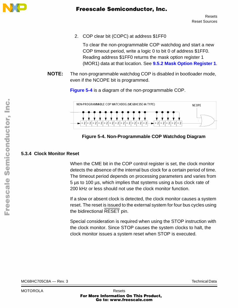
ResetsReset Sources
F
ree
sca
le S
em
ico
nd
uc
tor,
I
Freescale Semiconductor, Inc.n
c..
.
2. COP clear bit (COPC) at address $1FF0
To clear the non-programmable COP watchdog and start a new COP timeout period, write a logic 0 to bit 0 of address $1FF0. Reading address $1FF0 returns the mask option register 1 (MOR1) data at that location. See 9.5.2 Mask Option Register 1.
NOTE: The non-programmable watchdog COP is disabled in bootloader mode, even if the NCOPE bit is programmed.
Figure 5-4 is a diagram of the non-programmable COP.
Figure 5-4. Non-Programmable COP Watchdog Diagram
5.3.4 Clock Monitor Reset
When the CME bit in the COP control register is set, the clock monitor detects the absence of the internal bus clock for a certain period of time. The timeout period depends on processing parameters and varies from 5 µs to 100 µs, which implies that systems using a bus clock rate of 200 kHz or less should not use the clock monitor function.
If a slow or absent clock is detected, the clock monitor causes a system reset. The reset is issued to the external system for four bus cycles using the bidirectional RESET pin.
Special consideration is required when using the STOP instruction with the clock monitor. Since STOP causes the system clocks to halt, the clock monitor issues a system reset when STOP is executed.
÷ 2÷ 2 ÷ 2 ÷ 2 ÷ 2 ÷ 2 ÷ 2 ÷ 2 ÷ 2 ÷ 2 ÷ 2 ÷ 2 ÷ 2 ÷ 2 ÷ 2 ÷ 2÷ 2
NCOPE NON-PROGRAMMABLE COP WATCHDOG (MC68HC05C4A TYPE)
MC68HC705C8A — Rev. 3 Technical Data
MOTOROLA Resets For More Information On This Product,
Go to: www.freescale.com
Resets
F
ree
sca
le S
em
ico
nd
uc
tor,
I
Freescale Semiconductor, Inc.n
c..
.
The clock monitor is a useful backup to the COP watchdog system. Because the watchdog timer requires a clock to function, it cannot indicate a system clock failure. The clock monitor would detect such a condition and force the MCU to a reset state. Clocks are not required for the MCU to reach a reset condition. They are, however, required to bring the MCU through the reset sequence and back to run condition.
Technical Data MC68HC705C8A — Rev. 3
68 Resets For More Information On This Product,
Go to: www.freescale.com

F
ree
sca
le S
em
ico
nd
uc
tor,
IFreescale Semiconductor, Inc.
nc
...
Technical Data — MC68HC705C8A
Section 6. Low-Power Modes
6.1 Contents
6.2 Introduction . . . . . . . . . . . . . . . . . . . . . . . . . . . . . . . . . . . . . . . .69
6.3 Stop Mode . . . . . . . . . . . . . . . . . . . . . . . . . . . . . . . . . . . . . . . .696.3.1 SCI During Stop Mode . . . . . . . . . . . . . . . . . . . . . . . . . . . . .716.3.2 SPI During Stop Mode . . . . . . . . . . . . . . . . . . . . . . . . . . . . .716.3.3 Programmable COP Watchdog in Stop Mode . . . . . . . . . . .716.3.4 Non-Programmable COP Watchdog in Stop Mode . . . . . . .73
6.4 Wait Mode. . . . . . . . . . . . . . . . . . . . . . . . . . . . . . . . . . . . . . . . .736.4.1 Programmable COP Watchdog in Wait Mode . . . . . . . . . . .756.4.2 Non-Programmable COP Watchdog in Wait Mode . . . . . . .75
6.5 Data-Retention Mode . . . . . . . . . . . . . . . . . . . . . . . . . . . . . . . .75
6.2 Introduction
This section describes the three low-power modes:
• Stop mode
• Wait mode
• Data-retention mode
6.3 Stop Mode
The STOP instruction places the microcontroller unit (MCU) in its lowest power consumption mode. In stop mode, the internal oscillator is turned off, halting all internal processing including timer, serial communications interface (SCI), and master mode serial peripheral interface (SPI) operation. See Figure 6-1.
MC68HC705C8A — Rev. 3 Technical Data
MOTOROLA Low-Power Modes For More Information On This Product,
Go to: www.freescale.com

Low-Power Modes
F
ree
sca
le S
em
ico
nd
uc
tor,
I
Freescale Semiconductor, Inc.n
c..
.
Figure 6-1. Stop/Wait Mode Function Flowchart
During stop mode, the I bit in the condition code register (CCR) is cleared to enable external interrupts. All other registers and memory remain unaltered. All input/output (I/O) lines remain unchanged. The processor can be brought out of stop mode only by an external interrupt or reset.
NO
YES
YES
YES
YES
YES
NO
NO
NONO
YES
NO
NOYES
STOP
RESET
EXTERNALINTERRUPT
(IRQ)
TURN ON OSCILLATORWAIT FOR TIME
DELAY TO STABILIZE
1. FETCH RESET VECTOR
2. SERVICE INTERRUPT:a. STACKb. SET I BITc. VECTOR TO
INTERRUPT ROUTINE
STOP OSCILLATORAND ALL CLOCKS
CLEAR I BIT
WAIT
OSCILLATOR ACTIVETIMER, SCI, AND SPI
CLOCKS ACTIVECPU CLOCKS STOPPED
RESET
EXTERNALINTERRUPT
(IRQ)
INTERNAL TIMERINTERRUPT
INTERNAL SCIINTERRUPT
INTERNAL SPIINTERRUPT
RESTART CPU CLOCK
1. FETCH RESET VECTOR
2. SERVICE INTERRUPT:a. STACKb. SET I BITc. VECTOR TO
INTERRUPT ROUTINE
CLEAR I BIT
OR OR
Technical Data MC68HC705C8A — Rev. 3
70 Low-Power Modes For More Information On This Product,
Go to: www.freescale.com

Low-Power ModesStop Mode
F
ree
sca
le S
em
ico
nd
uc
tor,
I
Freescale Semiconductor, Inc.n
c..
.
6.3.1 SCI During Stop Mode
When the MCU enters stop mode, the baud rate generator stops, halting all SCI activity. If the STOP instruction is executed during a transmitter transfer, that transfer is halted. If a low input to the IRQ pin is used to exit stop mode, the transfer resumes.
If the SCI receiver is receiving data and stop mode is entered, received data sampling stops because the baud rate generator stops, and all subsequent data is lost. Therefore, all SCI transfers should be in the idle state when the STOP instruction is executed.
6.3.2 SPI During Stop Mode
When the MCU enters stop mode, the baud rate generator stops, terminating all master mode SPI operations. If the STOP instruction is executed during an SPI transfer, that transfer halts until the MCU exits stop mode by a low signal on the IRQ pin. If reset is used to exit stop mode, the SPI control and status bits are cleared, and the SPI is disabled.
If the MCU is in slave mode when the STOP instruction is executed, the slave SPI continues to operate and can still accept data and clock information in addition to transmitting its own data back to a master device. At the end of a possible transmission with a slave SPI in stop mode, no flags are set until a low on the IRQ pin wakes up the MCU.
NOTE: Although a slave SPI in stop mode can exchange data with a master SPI, the status bits of a slave SPI are inactive in stop mode.
6.3.3 Programmable COP Watchdog in Stop Mode
The STOP instruction turns off the internal oscillator and suspends the computer operating properly (COP) watchdog counter. If the RESET pin brings the MCU out of stop mode, the reset function clears and disables the COP watchdog.
If the IRQ pin brings the MCU out of stop mode, the COP counter resumes counting from its suspended value after the 4064-tCYC clock stabilization delay. See Figure 6-2.
MC68HC705C8A — Rev. 3 Technical Data
MOTOROLA Low-Power Modes For More Information On This Product,
Go to: www.freescale.com

Low-Power Modes
F
ree
sca
le S
em
ico
nd
uc
tor,
I
Freescale Semiconductor, Inc.n
c..
.
NOTE: If the clock monitor is enabled (CME = 1), the STOP instruction causes the clock monitor to time out and reset the MCU.
Figure 6-2. Programmable COP Watchdog in Stop Mode (PCOPE = 1) Flowchart
STABILIZATION
STOP
EXTERNALRESET?
NO
NO
TURN ON INTERNAL OSCILLATOR
YES
YES
END OF
DELAY?
YES
NO
1. LOAD PC WITH RESET VECTOROR
2. SERVICE INTERRUPT:a. SAVE CPU REGISTERS ON STACKb. SET I BIT IN CCRc. LOAD PC WITH INTERRUPT VECTOR
CLEAR I BIT IN CCRTURN OFF INTERNAL OSCILLATOR
TURN ON INTERNAL CLOCK
SUSPEND COP COUNTER
TURN ON INTERNAL OSCILLATOR
END OFSTABILIZATION
DELAY?
YES
NO
1. LOAD PC WITH RESET VECTOROR
2. SERVICE INTERRUPT:a. SAVE CPU REGISTERS ON STACKb. SET I BIT IN CCRc. LOAD PC WITH INTERRUPT VECTOR
TURN ON INTERNAL CLOCK
CLEAR COP COUNTERCLEAR PCOPE BIT IN COPCR
RESUME COP WATCHDOG COUNT
EXTERNALINTERRUPT?
Technical Data MC68HC705C8A — Rev. 3
72 Low-Power Modes For More Information On This Product,
Go to: www.freescale.com

Low-Power ModesWait Mode
F
ree
sca
le S
em
ico
nd
uc
tor,
I
Freescale Semiconductor, Inc.n
c..
.
6.3.4 Non-Programmable COP Watchdog in Stop Mode
The STOP instruction has these effects on the non-programmable COP watchdog:
• Turns off the oscillator and the COP watchdog counter
• Clears the COP watchdog counter
If the RESET pin brings the MCU out of stop mode, the COP watchdog begins counting immediately. The reset function clears the COP counter again after the 4064-tCYC clock stabilization delay.
If the IRQ pin brings the MCU out of stop mode, the COP watchdog begins counting immediately. The IRQ function does not clear the COP counter again after the 4064-tCYC clock stabilization delay. See Figure 6-3.
NOTE: If the clock monitor is enabled (CME = 1), the STOP instruction causes it to time out and reset the MCU.
6.4 Wait Mode
The WAIT instruction places the MCU in an intermediate power consumption mode. All central processor unit (CPU) activity is suspended, but the oscillator, capture/compare timer, SCI, and SPI remain active. Any interrupt or reset brings the MCU out of wait mode. See Figure 6-1.
The WAIT instruction has these effects on the CPU:
• Clears the I bit in the condition code register, enabling interrupts
• Stops the CPU clock, but allows the internal clock to drive the capture/compare timer, SCI, and SPI
The WAIT instruction does not affect any other registers or I/O lines. The capture/compare timer, SCI, and SPI can be enabled to allow a periodic exit from wait mode.
MC68HC705C8A — Rev. 3 Technical Data
MOTOROLA Low-Power Modes For More Information On This Product,
Go to: www.freescale.com
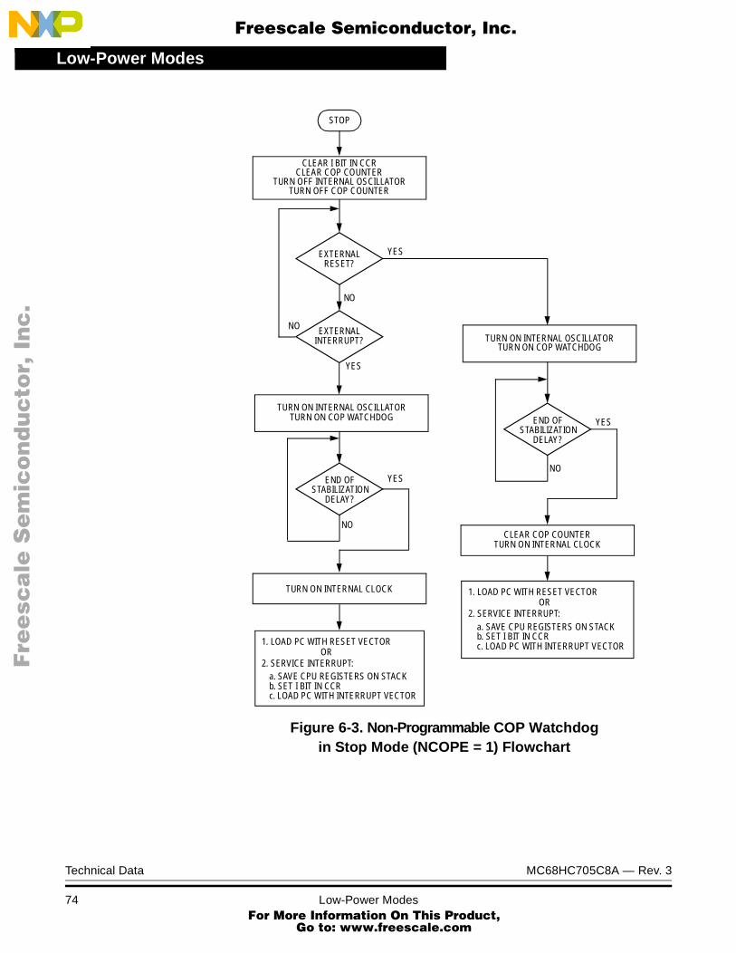
Low-Power Modes
F
ree
sca
le S
em
ico
nd
uc
tor,
I
Freescale Semiconductor, Inc.n
c..
.
Figure 6-3. Non-Programmable COP Watchdogin Stop Mode (NCOPE = 1) Flowchart
STABILIZATION
STOP
EXTERNALRESET?
NO
NO
TURN ON INTERNAL OSCILLATOR
YES
YES
END OF
DELAY?
YES
NO
1. LOAD PC WITH RESET VECTOROR
2. SERVICE INTERRUPT:a. SAVE CPU REGISTERS ON STACKb. SET I BIT IN CCRc. LOAD PC WITH INTERRUPT VECTOR
CLEAR I BIT IN CCRCLEAR COP COUNTER
TURN ON INTERNAL CLOCK
TURN OFF INTERNAL OSCILLATOR
TURN ON INTERNAL OSCILLATOR
END OFSTABILIZATION
DELAY?
YES
NO
1. LOAD PC WITH RESET VECTOROR
2. SERVICE INTERRUPT:a. SAVE CPU REGISTERS ON STACKb. SET I BIT IN CCRc. LOAD PC WITH INTERRUPT VECTOR
CLEAR COP COUNTER
TURN ON COP WATCHDOG
EXTERNALINTERRUPT?
TURN OFF COP COUNTER
TURN ON COP WATCHDOG
TURN ON INTERNAL CLOCK
Technical Data MC68HC705C8A — Rev. 3
74 Low-Power Modes For More Information On This Product,
Go to: www.freescale.com
Low-Power ModesData-Retention Mode
F
ree
sca
le S
em
ico
nd
uc
tor,
I
Freescale Semiconductor, Inc.n
c..
.
6.4.1 Programmable COP Watchdog in Wait Mode
The programmable COP watchdog is active during wait mode. Software must periodically bring the MCU out of wait mode to clear the programmable COP watchdog.
6.4.2 Non-Programmable COP Watchdog in Wait Mode
The non-programmable COP watchdog is active during wait mode. Software must periodically bring the MCU out of wait mode to clear the non-programmable COP watchdog.
6.5 Data-Retention Mode
In data-retention mode, the MCU retains random-access memory (RAM) contents and CPU register contents at VDD voltages as low as 2.0 Vdc. The data-retention feature allows the MCU to remain in a low power-consumption state during which it retains data, but the CPU cannot execute instructions.
To put the MCU in data-retention mode:
1. Drive the RESET pin to logic 0.
2. Lower VDD voltage. The RESET pin must remain low continuously during data-retention mode.
To take the MCU out of data-retention mode:
1. Return VDD to normal operating voltage.
2. Return the RESET pin to logic 1.
MC68HC705C8A — Rev. 3 Technical Data
MOTOROLA Low-Power Modes For More Information On This Product,
Go to: www.freescale.com
Low-Power Modes
F
ree
sca
le S
em
ico
nd
uc
tor,
I
Freescale Semiconductor, Inc.n
c..
.
Technical Data MC68HC705C8A — Rev. 3
76 Low-Power Modes For More Information On This Product,
Go to: www.freescale.com

F
ree
sca
le S
em
ico
nd
uc
tor,
IFreescale Semiconductor, Inc.
nc
...
Technical Data — MC68HC705C8A
Section 7. Parallel Input/Output (I/O)
7.1 Contents
7.2 Introduction . . . . . . . . . . . . . . . . . . . . . . . . . . . . . . . . . . . . . . . .77
7.3 Port A . . . . . . . . . . . . . . . . . . . . . . . . . . . . . . . . . . . . . . . . . . . .787.3.1 Port A Data Register . . . . . . . . . . . . . . . . . . . . . . . . . . . . . .787.3.2 Data Direction Register A. . . . . . . . . . . . . . . . . . . . . . . . . . .797.3.3 Port A Logic . . . . . . . . . . . . . . . . . . . . . . . . . . . . . . . . . . . . .80
7.4 Port B . . . . . . . . . . . . . . . . . . . . . . . . . . . . . . . . . . . . . . . . . . . .817.4.1 Port B Data Register . . . . . . . . . . . . . . . . . . . . . . . . . . . . . .817.4.2 Data Direction Register B. . . . . . . . . . . . . . . . . . . . . . . . . . .827.4.3 Port B Logic . . . . . . . . . . . . . . . . . . . . . . . . . . . . . . . . . . . . .83
7.5 Port C . . . . . . . . . . . . . . . . . . . . . . . . . . . . . . . . . . . . . . . . . . . .857.5.1 Port C Data Register . . . . . . . . . . . . . . . . . . . . . . . . . . . . . .857.5.2 Data Direction Register C. . . . . . . . . . . . . . . . . . . . . . . . . . .867.5.3 Port C Logic . . . . . . . . . . . . . . . . . . . . . . . . . . . . . . . . . . . . .87
7.6 Port D . . . . . . . . . . . . . . . . . . . . . . . . . . . . . . . . . . . . . . . . . . . .88
7.2 Introduction
This section describes the programming of ports A, B, C, and D.
MC68HC705C8A — Rev. 3 Technical Data
MOTOROLA Parallel Input/Output (I/O) For More Information On This Product,
Go to: www.freescale.com

Parallel Input/Output (I/O)
F
ree
sca
le S
em
ico
nd
uc
tor,
I
Freescale Semiconductor, Inc.n
c..
.
7.3 Port A
Port A is an 8-bit, general-purpose, bidirectional input/output (I/O) port.
7.3.1 Port A Data Register
The port A data register (PORTA) shown in Figure 7-1 contains a data latch for each of the eight port A pins. When a port A pin is programmed to be an output, the state of its data register bit determines the state of the output pin. When a port A pin is programmed to be an input, reading the port A data register returns the logic state of the pin.
PA7–PA0 — Port A Data Bits
These read/write bits are software programmable. Data direction of each bit is under the control of the corresponding bit in data direction register A. Reset has no effect on port A data.
Address: $0000
Bit 7 6 5 4 3 2 1 Bit 0
Read:PA7 PA6 PA5 PA4 PA3 PA2 PA1 PA0
Write:
Reset: Unaffected by reset
Figure 7-1. Port A Data Register (PORTA)
Technical Data MC68HC705C8A — Rev. 3
78 Parallel Input/Output (I/O) For More Information On This Product,
Go to: www.freescale.com

Parallel Input/Output (I/O)Port A
F
ree
sca
le S
em
ico
nd
uc
tor,
I
Freescale Semiconductor, Inc.n
c..
.
7.3.2 Data Direction Register A
The contents of data direction register A (DDRA) shown in Figure 7-2 determine whether each port A pin is an input or an output. Writing a logic 1 to a DDRA bit enables the output buffer for the associated port A pin; a logic 0 disables the output buffer. A reset clears all DDRA bits, configuring all port A pins as inputs.
DDRA7–DDRA0 — Port A Data Direction Bits
These read/write bits control port A data direction. Reset clears bits DDRA7–DDRA0.
1 = Corresponding port A pin configured as output0 = Corresponding port A pin configured as input
NOTE: Avoid glitches on port A pins by writing to the port A data register before changing DDRA bits from logic 0 to logic 1.
Address: $0004
Bit 7 6 5 4 3 2 1 Bit 0
Read:DDRA7 DDRA6 DDRA5 DDRA4 DDRA3 DDRA2 DDRA1 DDRA0
Write:
Reset: 0 0 0 0 0 0 0 0
Figure 7-2. Data Direction Register A (DDRA)
MC68HC705C8A — Rev. 3 Technical Data
MOTOROLA Parallel Input/Output (I/O) For More Information On This Product,
Go to: www.freescale.com

Parallel Input/Output (I/O)
F
ree
sca
le S
em
ico
nd
uc
tor,
I
Freescale Semiconductor, Inc.n
c..
.
7.3.3 Port A Logic
Figure 7-3 is a diagram of the port A I/O logic.
Figure 7-3. Port A I/O Logic
When a port A pin is programmed to be an output, the state of its data register bit determines the state of the output pin. When a port A pin is programmed to be an input, reading the port A data register returns the logic state of the pin.
The data latch can always be written, regardless of the state of its DDRA bit. Table 7-1 summarizes the operation of the port A pins.
NOTE: To avoid excessive current draw, tie all unused input pins to VDD or VSS, or change I/O pins to outputs by writing to DDRA in user code as early as possible.
Table 7-1. Port A Pin Functions
DDRA Bit I/O Pin ModeAccesses to DDRA Accesses to PORTA
Read/Write Read Write
0 Input, Hi-Z(1)
1. Hi-Z = high impedance
DDRA7–DDRA0 Pin PA7–PA0(2)
2. Writing affects data register but does not affect input.
1 Output DDRA7–DDRA0 PA7–PA0 PA7–PA0
DATA DIRECTIONREGISTER ABIT DDRAx
PAxPORT A DATA
REGISTERBIT PAx
READ $0004
WRITE $0000
READ $0000
RESETIN
TERN
AL D
ATA
BUS
WRITE $0004
Technical Data MC68HC705C8A — Rev. 3
80 Parallel Input/Output (I/O) For More Information On This Product,
Go to: www.freescale.com

Parallel Input/Output (I/O)Port B
F
ree
sca
le S
em
ico
nd
uc
tor,
I
Freescale Semiconductor, Inc.n
c..
.
7.4 Port B
Port B is an 8-bit, general-purpose, bidirectional I/O port. Port B pins can also be configured to function as external interrupts. The port B pullup devices are enabled in mask option register 1 (MOR1). See 9.5.2 Mask Option Register 1 and 4.3.3 Port B Interrupts.
7.4.1 Port B Data Register
The port B data register (PORTB) shown in Figure 7-4 contains a data latch for each of the eight port B pins.
PB7–PB0 — Port B Data Bits
These read/write bits are software programmable. Data direction of each bit is under the control of the corresponding bit in data direction register B. Reset has no effect on port B data.
Address: $0001
Bit 7 6 5 4 3 2 1 Bit 0
Read:PB7 PB6 PB5 PB4 PB3 PB2 PB1 PB0
Write:
Reset: Unaffected by reset
Figure 7-4. Port B Data Register (PORTB)
MC68HC705C8A — Rev. 3 Technical Data
MOTOROLA Parallel Input/Output (I/O) For More Information On This Product,
Go to: www.freescale.com
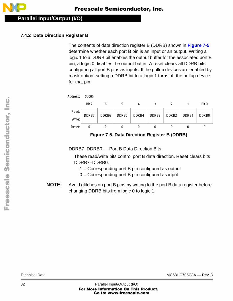
Parallel Input/Output (I/O)
F
ree
sca
le S
em
ico
nd
uc
tor,
I
Freescale Semiconductor, Inc.n
c..
.
7.4.2 Data Direction Register B
The contents of data direction register B (DDRB) shown in Figure 7-5 determine whether each port B pin is an input or an output. Writing a logic 1 to a DDRB bit enables the output buffer for the associated port B pin; a logic 0 disables the output buffer. A reset clears all DDRB bits, configuring all port B pins as inputs. If the pullup devices are enabled by mask option, setting a DDRB bit to a logic 1 turns off the pullup device for that pin.
DDRB7–DDRB0 — Port B Data Direction Bits
These read/write bits control port B data direction. Reset clears bits DDRB7–DDRB0.
1 = Corresponding port B pin configured as output0 = Corresponding port B pin configured as input
NOTE: Avoid glitches on port B pins by writing to the port B data register before changing DDRB bits from logic 0 to logic 1.
Address: $0005
Bit 7 6 5 4 3 2 1 Bit 0
Read:DDRB7 DDRB6 DDRB5 DDRB4 DDRB3 DDRB2 DDRB1 DDRB0
Write:
Reset: 0 0 0 0 0 0 0 0
Figure 7-5. Data Direction Register B (DDRB)
Technical Data MC68HC705C8A — Rev. 3
82 Parallel Input/Output (I/O) For More Information On This Product,
Go to: www.freescale.com

Parallel Input/Output (I/O)Port B
F
ree
sca
le S
em
ico
nd
uc
tor,
I
Freescale Semiconductor, Inc.n
c..
.
7.4.3 Port B Logic
Figure 7-6 shows the port B I/O logic.
Figure 7-6. Port B I/O Logic
PB7
EXTERNALINTERRUPTREQUEST
DATA DIRECTIONREGISTER BBIT DDRB7
PORT B DATAREGISTER
BIT PB7
READ $0005
WRITE $0001
READ $0001
RESET
INTE
RN
AL D
ATA
BUS
WRITE $0005
PBPU7
FROM OTHER
VDD
PORT B PINS
D
C
Q
RQ
I BIT
VDD
FROM CCR
RESET
EXTERNAL INTERRUPT VECTOR FETCH
IRQ
IRQ
FROM OPTIONREGISTER
IRQLATCH
FROM MOR1
MC68HC705C8A — Rev. 3 Technical Data
MOTOROLA Parallel Input/Output (I/O) For More Information On This Product,
Go to: www.freescale.com

Parallel Input/Output (I/O)
F
ree
sca
le S
em
ico
nd
uc
tor,
I
Freescale Semiconductor, Inc.n
c..
.
When a port B pin is programmed as an output, reading the port bit reads the value of the data latch and not the voltage on the pin itself. When a port B pin is programmed as an input, reading the port bit reads the voltage level on the pin. The data latch can always be written, regardless of the state of its DDRB bit.
NOTE: To avoid excessive current draw, tie all unused input pins to VDD or VSS, or for I/O pins change to outputs by writing to DDRB in user code as early as possible.
Table 7-2. Port B Pin Functions
DDRB Bit I/O Pin ModeAccesses to DDRB Accesses to PORTB
Read/Write Read Write
0 Input, Hi-Z(1)
1. Hi-Z = high impedance
DDRB7–DDRB0 Pin PB7–PB0(2)
2. Writing affects data register but does not affect input.
1 Output DDRB7–DDRB0 PB7–PB0 PB7–PB0
Technical Data MC68HC705C8A — Rev. 3
84 Parallel Input/Output (I/O) For More Information On This Product,
Go to: www.freescale.com

Parallel Input/Output (I/O)Port C
F
ree
sca
le S
em
ico
nd
uc
tor,
I
Freescale Semiconductor, Inc.n
c..
.
7.5 Port C
Port C is an 8-bit, general-purpose, bidirectional I/O port. PC7 has a high current sink and source capability.
7.5.1 Port C Data Register
The port C data register (PORTC) shown in Figure 7-7 contains a data latch for each of the eight port C pins. When a port C pin is programmed to be an output, the state of its data register bit determines the state of the output pin. When a port C pin is programmed to be an input, reading the port C data register returns the logic state of the pin.
PC7–PC0 — Port C Data Bits
These read/write bits are software programmable. Data direction of each bit is under the control of the corresponding bit in data direction register C. PC7 has a high current sink and source capability. Reset has no effect on port C data.
Address: $0002
Bit 7 6 5 4 3 2 1 Bit 0
Read:PC7 PC6 PC5 PC4 PC3 PC2 PC1 PC0
Write:
Reset: Unaffected by reset
Figure 7-7. Port C Data Register (PORTC)
MC68HC705C8A — Rev. 3 Technical Data
MOTOROLA Parallel Input/Output (I/O) For More Information On This Product,
Go to: www.freescale.com

Parallel Input/Output (I/O)
F
ree
sca
le S
em
ico
nd
uc
tor,
I
Freescale Semiconductor, Inc.n
c..
.
7.5.2 Data Direction Register C
The contents of data direction register C (DDRC) shown in Figure 7-8 determine whether each port C pin is an input or an output. Writing a logic 1 to a DDRC bit enables the output buffer for the associated port C pin; a logic 0 disables the output buffer. A reset clears all DDRC bits, configuring all port C pins as inputs.
DDRC7–DDRC0 — Port C Data Direction Bits
These read/write bits control port C data direction. Reset clears bits DDRC7–DDRC0.
1 = Corresponding port C pin configured as output0 = Corresponding port C pin configured as input
NOTE: Avoid glitches on port C pins by writing to the port C data register before changing DDRC bits from logic 0 to logic 1.
Address: $0006
Bit 7 6 5 4 3 2 1 Bit 0
Read:DDRC7 DDRC6 DDRC5 DDRC4 DDRC3 DDRC2 DDRC1 DDRC0
Write:
Reset: 0 0 0 0 0 0 0 0
Figure 7-8. Data Direction Register C (DDRC)
Technical Data MC68HC705C8A — Rev. 3
86 Parallel Input/Output (I/O) For More Information On This Product,
Go to: www.freescale.com

Parallel Input/Output (I/O)Port C
F
ree
sca
le S
em
ico
nd
uc
tor,
I
Freescale Semiconductor, Inc.n
c..
.
7.5.3 Port C Logic
Figure 7-9 shows port C I/O logic.
Figure 7-9. Port C I/O Logic
When a port C pin is programmed as an output, reading the port bit reads the value of the data latch and not the voltage on the pin. When a port C pin is programmed as an input, reading the port bit reads the voltage level on the pin. The data latch can always be written, regardless of the state of its DDRC bit. Table 7-3 summarizes the operation of the port C pins.
NOTE: To avoid excessive current draw, tie all unused input pins to VDD or VSS or change I/O pins to outputs by writing to DDRC in user code as early as possible.
Table 7-3. Port C Pin Functions
DDRC Bit I/O Pin ModeAccesses to DDRC Accesses to PORTC
Read/Write Read Write
0 Input, Hi-Z(1)
1. Hi-Z = high impedance
DDRC7–DDRC0 Pin PC7–PC0(2)
2. Writing affects data register but does not affect input.
1 Output DDRC7–DDRC0 PC7–PC0 PC7–PC0
PCx
DATA DIRECTIONREGISTER CBIT DDRCx
PORT C DATAREGISTER
BIT PCx
READ $0006
WRITE $0002
READ $0002
RESETIN
TERN
AL D
ATA
BUS
WRITE $0006
MC68HC705C8A — Rev. 3 Technical Data
MOTOROLA Parallel Input/Output (I/O) For More Information On This Product,
Go to: www.freescale.com

Parallel Input/Output (I/O)
F
ree
sca
le S
em
ico
nd
uc
tor,
I
Freescale Semiconductor, Inc.n
c..
.
7.6 Port D
Port D is a 7-bit, special-purpose, input-only port that has no data register. Reading address $0003 returns the logic states of the port D pins.
Port D shares pins PD5–PD2 with the serial peripheral interface module (SPI). When the SPI is enabled, PD5–PD2 read as logic 0s. When the SPI is disabled, reading address $0003 returns the logic states of the PD5–PD2 pins.
Port D shares pins PD1 and PD0 with the SCI module. When the SCI is enabled, PD1 and PD0 read as logic 0s. When the SCI is disabled, reading address $0003 returns the logic states of the PD1 and PD0 pins.
Address: $0003
Bit 7 6 5 4 3 2 1 Bit 0
Read: PD7 SS SCK MOSI MISO TDO RDI
Write:
Reset: Unaffected by reset
= Unimplemented
Figure 7-10. Port D Fixed Input Register (PORTD)
Technical Data MC68HC705C8A — Rev. 3
88 Parallel Input/Output (I/O) For More Information On This Product,
Go to: www.freescale.com

F
ree
sca
le S
em
ico
nd
uc
tor,
IFreescale Semiconductor, Inc.
nc
...
Technical Data — MC68HC705C8A
Section 8. Capture/Compare Timer
8.1 Contents
8.2 Introduction . . . . . . . . . . . . . . . . . . . . . . . . . . . . . . . . . . . . . . . .89
8.3 Timer Operation . . . . . . . . . . . . . . . . . . . . . . . . . . . . . . . . . . . .898.3.1 Input Capture . . . . . . . . . . . . . . . . . . . . . . . . . . . . . . . . . . . .928.3.2 Output Compare. . . . . . . . . . . . . . . . . . . . . . . . . . . . . . . . . .93
8.4 Timer I/O Registers. . . . . . . . . . . . . . . . . . . . . . . . . . . . . . . . . .948.4.1 Timer Control Register . . . . . . . . . . . . . . . . . . . . . . . . . . . . .948.4.2 Timer Status Register . . . . . . . . . . . . . . . . . . . . . . . . . . . . .968.4.3 Timer Registers . . . . . . . . . . . . . . . . . . . . . . . . . . . . . . . . . .978.4.4 Alternate Timer Registers. . . . . . . . . . . . . . . . . . . . . . . . . . .988.4.5 Input Capture Registers . . . . . . . . . . . . . . . . . . . . . . . . . .1008.4.6 Output Compare Registers. . . . . . . . . . . . . . . . . . . . . . . . .101
8.2 Introduction
This section describes the operation of the 16-bit capture/compare timer. Figure 8-1 shows the structure of the timer module. Figure 8-2 is a summary of the timer input/output (I/O) registers.
8.3 Timer Operation
The core of the capture/compare timer is a 16-bit free-running counter. The counter is the timing reference for the input capture and output compare functions. The input capture and output compare functions can latch the times at which external events occur, measure input waveforms, and generate output waveforms and timing delays. Software can read the value in the counter at any time without affecting the counter sequence.
MC68HC705C8A — Rev. 3 Technical Data
MOTOROLA Capture/Compare Timer For More Information On This Product,
Go to: www.freescale.com

Capture/Compare Timer
F
ree
sca
le S
em
ico
nd
uc
tor,
I
Freescale Semiconductor, Inc.n
c..
.
Figure 8-1. Timer Block Diagram
TCAP
EDGESELECT/
16-BIT COMPARATOR
OCRH ($0016) OCRL ($0017)
16-BIT COUNTER
ATRH ($001A) ATRL ($001B)
TCMP
DETECTLOGIC
PINCONTROL
LOGIC
TRH ($0018) TRL ($0019)
ICRH ($0014) ICRL ($0015)
INTERNAL DATA BUS
TIMER CONTROL REGISTER TIMER STATUS REGISTER
TIMERINTERRUPTREQUEST
INTERNAL CLOCK (XTAL ÷ 2)
TOF
OC
F
ICF
$0013$0012
ICIE
OC
IE
TOIE
IED
G
OLV
L
OVE
RFLO
W
÷ 4
Technical Data MC68HC705C8A — Rev. 3
90 Capture/Compare Timer For More Information On This Product,
Go to: www.freescale.com

Capture/Compare TimerTimer Operation
F
ree
sca
le S
em
ico
nd
uc
tor,
I
Freescale Semiconductor, Inc.n
c..
.
Addr. Register Name Bit 7 6 5 4 3 2 1 Bit 0
$0012Timer Control Register
(TCR)See page 94.
Read:ICIE OCIE TOIE 0 0 0 IEDG OLVL
Write:
Reset: 0 0 0 0 0 0 U 0
$0013Timer Status Register
(TSR)See page 96.
Read: ICF OCF TOF 0 0 0 0 0
Write:
Reset: U U U 0 0 0 0 0
$0014Input Capture Register
High (ICRH)See page 100.
Read: Bit 15 Bit 14 Bit 13 Bit 12 Bit 11 Bit 10 Bit 9 Bit 8
Write:
Reset: Unaffected by reset
$0015Input Capture Register
Low (ICRL)See page 100.
Read: Bit 7 Bit 6 Bit 5 Bit 4 Bit 3 Bit 2 Bit 1 Bit 0
Write:
Reset: Unaffected by reset
$0016
Output Compare RegisterHigh (OCRH)
See page 101.
Read:Bit 15 Bit 14 Bit 13 Bit 12 Bit 11 Bit 10 Bit 9 Bit 8
Write:
Reset: Unaffected by reset
$0017Output Compare Register
Low (OCRL)See page 101.
Read:Bit 7 Bit 6 Bit 5 Bit 4 Bit 3 Bit 2 Bit 1 Bit 0
Write:
Reset: Unaffected by reset
$0018Timer Register High
(TRH)See page 97.
Read: Bit 15 Bit 14 Bit 13 Bit 12 Bit 11 Bit 10 Bit 9 Bit 8
Write:
Reset: Reset initializes TRH to $FF
$0019Timer Register Low
(TRL)See page 97.
Read: Bit 7 Bit 6 Bit 5 Bit 4 Bit 3 Bit 2 Bit 1 Bit 0
Write:
Reset: Reset initializes TRL to $FC
$001AAlternate Timer Register
High (ATRH)See page 99.
Read: Bit 15 Bit 14 Bit 13 Bit 12 Bit 11 Bit 10 Bit 9 Bit 8
Write:
Reset: Reset initializes ATRH to $FF
$001BAlternate Timer Register
Low (ATRL)See page 99.
Read: Bit 7 Bit 6 Bit 5 Bit 4 Bit 3 Bit 2 Bit 1 Bit 0
Write:
Reset: Reset initializes ATRL to $FC
= Unimplemented U = Unaffected
Figure 8-2. Timer I/O Register Summary
MC68HC705C8A — Rev. 3 Technical Data
MOTOROLA Capture/Compare Timer For More Information On This Product,
Go to: www.freescale.com

Capture/Compare Timer
F
ree
sca
le S
em
ico
nd
uc
tor,
I
Freescale Semiconductor, Inc.n
c..
.
Because of the 16-bit timer architecture, the I/O registers for the input capture and output compare functions are pairs of 8-bit registers.
Because the counter is 16 bits long and preceded by a fixed divide-by-four prescaler, the counter rolls over every 262,144 internal clock cycles. Timer resolution with a 4-MHz crystal is 2 µs.
8.3.1 Input Capture
The input capture function can record the time at which an external event occurs. When the input capture circuitry detects an active edge on the input capture pin (TCAP), it latches the contents of the timer registers into the input capture registers. The polarity of the active edge is programmable.
Latching values into the input capture registers at successive edges of the same polarity measures the period of the input signal on the TCAP pin. Latching the counter values at successive edges of opposite polarity measures the pulse width of the signal. Figure 8-3 shows the logic of the input capture function.
Figure 8-3. Input Capture Operation
TCAPEDGE
SELECT/DETECT INPUT CAPTURE REGISTER HIGH INPUT CAPTURE REGISTER LOW
TIMER REGISTER HIGH TIMER REGISTER LOW
TIMERINTERRUPTREQUEST
LOGIC
15 $0018 8 7 $0019 0
15 8 7 0
$0014 $0015
TIMER STATUS REGISTERTIMER CONTROL REGISTER
LATCH
IED
G$0012 $0013
ICF
OC
F
TOF
ICIE
OC
IE
TOIE
OLV
L
Technical Data MC68HC705C8A — Rev. 3
92 Capture/Compare Timer For More Information On This Product,
Go to: www.freescale.com

Capture/Compare TimerTimer Operation
F
ree
sca
le S
em
ico
nd
uc
tor,
I
Freescale Semiconductor, Inc.n
c..
.
8.3.2 Output Compare
The output compare function can generate an output signal when the 16-bit counter reaches a selected value. Software writes the selected value into the output compare registers. On every fourth internal clock cycle the output compare circuitry compares the value of the counter to the value written in the output compare registers. When a match occurs, the timer transfers the programmable output level bit (OLVL) from the timer control register to the output compare pin (TCMP).
Software can use the output compare register to measure time periods, to generate timing delays, or to generate a pulse of specific duration or a pulse train of specific frequency and duty cycle on the TCMP pin. Figure 8-4 shows the logic of the output compare function.
Figure 8-4. Output Compare Operation
16-BIT COMPARATOR
OUTPUT COMPARE REGISTER HIGH OUTPUT COMPARE REGISTER LOW
COUNTER HIGH BYTE COUNTER LOW BYTE
PINCONTROL
LOGICTCMP
TIMER STATUS REGISTERTIMER STATUS REGISTER
15 0
15 8 7 0
TIMERINTERRUPTREQUEST
ICIE
OC
IE
TOIE
ICF
OC
F
TOF
$0012 $0013
$0016 $0017
MC68HC705C8A — Rev. 3 Technical Data
MOTOROLA Capture/Compare Timer For More Information On This Product,
Go to: www.freescale.com

Capture/Compare Timer
F
ree
sca
le S
em
ico
nd
uc
tor,
I
Freescale Semiconductor, Inc.n
c..
.
8.4 Timer I/O Registers
These registers control and monitor the timer operation:
• Timer control register (TCR)
• Timer status register (TSR)
• Timer registers (TRH and TRL)
• Alternate timer registers (ATRH and ATRL)
• Input capture registers (ICRH and ICRL)
• Output compare registers (OCRH and OCRL)
8.4.1 Timer Control Register
The timer control register (TCR) as shown in Figure 8-5 performs these functions:
• Enables input capture interrupts
• Enables output compare interrupts
• Enables timer overflow interrupts
• Controls the active edge polarity of the TCAP signal
• Controls the active level of the TCMP output
Address: $0012
Bit 7 6 5 4 3 2 1 Bit 0
Read:ICIE OCIE TOIE 0 0 0 IEDG OLVL
Write:
Reset: 0 0 0 0 0 0 U 0
U = Unaffected
Figure 8-5. Timer Control Register (TCR)
Technical Data MC68HC705C8A — Rev. 3
94 Capture/Compare Timer For More Information On This Product,
Go to: www.freescale.com

Capture/Compare TimerTimer I/O Registers
F
ree
sca
le S
em
ico
nd
uc
tor,
I
Freescale Semiconductor, Inc.n
c..
.
ICIE — Input Capture Interrupt Enable Bit
This read/write bit enables interrupts caused by an active signal on the TCAP pin. Reset clears the ICIE bit.
1 = Input capture interrupts enabled0 = Input capture interrupts disabled
OCIE — Output Compare Interrupt Enable Bit
This read/write bit enables interrupts caused by an active signal on the TCMP pin. Reset clears the OCIE bit.
1 = Output compare interrupts enabled0 = Output compare interrupts disabled
TOIE — Timer Overflow Interrupt Enable Bit
This read/write bit enables interrupts caused by a timer overflow. Reset clears the TOIE bit.
1 = Timer overflow interrupts enabled0 = Timer overflow interrupts disabled
IEDG — Input Edge Bit
The state of this read/write bit determines whether a positive or negative transition on the TCAP pin triggers a transfer of the contents of the timer register to the input capture registers. Reset has no effect on the IEDG bit.
1 = Positive edge (low-to-high transition) triggers input capture0 = Negative edge (high-to-low transition) triggers input capture
OLVL — Output Level Bit
The state of this read/write bit determines whether a logic 1 or a logic 0 appears on the TCMP pin when a successful output compare occurs. Reset clears the OLVL bit.
1 = TCMP goes high on output compare0 = TCMP goes low on output compare
Bits 4–2 — Not used; these bits always read 0
MC68HC705C8A — Rev. 3 Technical Data
MOTOROLA Capture/Compare Timer For More Information On This Product,
Go to: www.freescale.com

Capture/Compare Timer
F
ree
sca
le S
em
ico
nd
uc
tor,
I
Freescale Semiconductor, Inc.n
c..
.
8.4.2 Timer Status Register
The timer status register (TSR) is a read-only register shown in Figure 8-6 contains flags for these events:
• An active signal on the TCAP pin, transferring the contents of the timer registers to the input capture registers
• A match between the 16-bit counter and the output compare registers, transferring the OLVL bit to the TCMP pin
• A timer rollover from $FFFF to $0000
ICF — Input Capture Flag
The ICF bit is set automatically when an edge of the selected polarity occurs on the TCAP pin. Clear the ICF bit by reading the timer status register with ICF set and then reading the low byte ($0015) of the input capture registers. Reset has no effect on ICF.
1 = Input capture0 = No input capture
OCF — Output Compare Flag
The OCF bit is set automatically when the value of the timer registers matches the contents of the output compare registers. Clear the OCF bit by reading the timer status register with OCF set and then reading the low byte ($0017) of the output compare registers. Reset has no effect on OCF.
1 = Output compare0 = No output compare
Address: $0013
Bit 7 6 5 4 3 2 1 Bit 0
Read: ICF OCF TOF 0 0 0 0 0
Write:
Reset: U U U 0 0 0 0 0
= Unimplemented U = Unaffected
Figure 8-6. Timer Status Register (TSR)
Technical Data MC68HC705C8A — Rev. 3
96 Capture/Compare Timer For More Information On This Product,
Go to: www.freescale.com

Capture/Compare TimerTimer I/O Registers
F
ree
sca
le S
em
ico
nd
uc
tor,
I
Freescale Semiconductor, Inc.n
c..
.
TOF — Timer Overflow Flag
The TOF bit is automatically set when the 16-bit counter rolls over from $FFFF to $0000. Clear the TOF bit by reading the timer status register with TOF set and then reading the low byte ($0019) of the timer registers. Reset has no effect on TOF.
1 = Timer overflow0 = No timer overflow
Bits 4–0 — Not used; these bits always read 0
8.4.3 Timer Registers
The read-only timer registers (TRH and TRL) shown in Figure 8-7 contain the current high and low bytes of the 16-bit counter. Reading TRH before reading TRL causes TRL to be latched until TRL is read. Reading TRL after reading the timer status register clears the timer overflow flag bit (TOF). Writing to the timer registers has no effect.
Bit 7 6 5 4 3 2 1 Bit 0
Register Name and Address: Timer Register High — $0018
Read: Bit 15 Bit 14 Bit 13 Bit 12 Bit 11 Bit 10 Bit 9 Bit 8
Write:
Reset: Reset initializes TRH to $FF
Register Name and Address: Timer Register Low — $0019
Read: Bit 7 Bit 6 Bit 5 Bit 4 Bit 3 Bit 2 Bit 1 Bit 0
Write:
Reset: Reset initializes TRL to $FC
= Unimplemented
Figure 8-7. Timer Registers (TRH and TRL)
MC68HC705C8A — Rev. 3 Technical Data
MOTOROLA Capture/Compare Timer For More Information On This Product,
Go to: www.freescale.com

Capture/Compare Timer
F
ree
sca
le S
em
ico
nd
uc
tor,
I
Freescale Semiconductor, Inc.n
c..
.
Reading TRH returns the current value of the high byte of the counter and causes the low byte to be latched into a buffer, as shown inFigure 8-8. The buffer value remains fixed even if the high byte is read more than once. Reading TRL reads the transparent low byte buffer and completes the read sequence of the timer registers.
Figure 8-8. Timer Register Reads
NOTE: To prevent interrupts from occurring between readings of TRH and TRL, set the interrupt mask (I bit) in the condition code register before reading TRH, and clear the mask after reading TRL.
8.4.4 Alternate Timer Registers
The alternate timer registers (ATRH and ATRL) shown in Figure 8-9 contain the current high and low bytes of the 16-bit counter. Reading ATRH before reading ATRL causes ATRL to be latched until ATRL is read. Reading does not affect the timer overflow flag (TOF). Writing to the alternate timer registers has no effect.
LOW BYTE BUFFER
$0018 $0019TIMER REGISTER HIGH TIMER REGISTER LOW
READ TRH
LATCH
INTERNAL DATA BUS
15
7 0
078
Technical Data MC68HC705C8A — Rev. 3
98 Capture/Compare Timer For More Information On This Product,
Go to: www.freescale.com
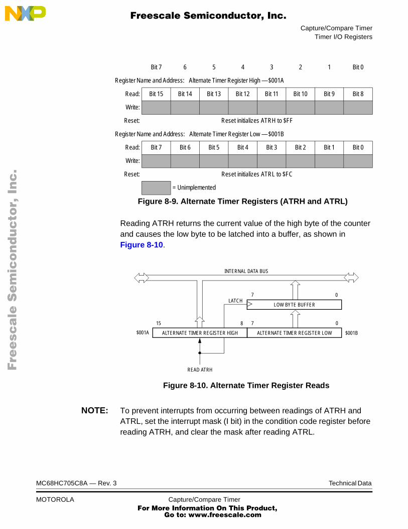
Capture/Compare TimerTimer I/O Registers
F
ree
sca
le S
em
ico
nd
uc
tor,
I
Freescale Semiconductor, Inc.n
c..
.
Reading ATRH returns the current value of the high byte of the counter and causes the low byte to be latched into a buffer, as shown inFigure 8-10.
Figure 8-10. Alternate Timer Register Reads
NOTE: To prevent interrupts from occurring between readings of ATRH and ATRL, set the interrupt mask (I bit) in the condition code register before reading ATRH, and clear the mask after reading ATRL.
Bit 7 6 5 4 3 2 1 Bit 0
Register Name and Address: Alternate Timer Register High — $001A
Read: Bit 15 Bit 14 Bit 13 Bit 12 Bit 11 Bit 10 Bit 9 Bit 8
Write:
Reset: Reset initializes ATRH to $FF
Register Name and Address: Alternate Timer Register Low — $001B
Read: Bit 7 Bit 6 Bit 5 Bit 4 Bit 3 Bit 2 Bit 1 Bit 0
Write:
Reset: Reset initializes ATRL to $FC
= Unimplemented
Figure 8-9. Alternate Timer Registers (ATRH and ATRL)
LOW BYTE BUFFER
$001A $001B
READ ATRH
LATCH
INTERNAL DATA BUS
15
7 0
078
ALTERNATE TIMER REGISTER HIGH ALTERNATE TIMER REGISTER LOW
MC68HC705C8A — Rev. 3 Technical Data
MOTOROLA Capture/Compare Timer For More Information On This Product,
Go to: www.freescale.com

Capture/Compare Timer
F
ree
sca
le S
em
ico
nd
uc
tor,
I
Freescale Semiconductor, Inc.n
c..
.
8.4.5 Input Capture Registers
When a selected edge occurs on the TCAP pin, the current high and low bytes of the 16-bit counter are latched into the read-only input capture registers (ICRH and ICRL) shown in Figure 8-11. Reading ICRH before reading ICRL inhibits further captures until ICRL is read. Reading ICRL after reading the timer status register clears the input capture flag (ICF). Writing to the input capture registers has no effect.
NOTE: To prevent interrupts from occurring between readings of ICRH and ICRL, set the interrupt mask (I bit) in the condition code register before reading ICRH and clear the mask after reading ICRL.
Bit 7 6 5 4 3 2 1 Bit 0
Register Name and Address: Input Capture Register High — $0014
Read: Bit 15 Bit 14 Bit 13 Bit 12 Bit 11 Bit 10 Bit 9 Bit 8
Write:
Reset: Unaffected by reset
Register Name and Address: Input Capture Register Low — $0015
Read: Bit 7 Bit 6 Bit 5 Bit 4 Bit 3 Bit 2 Bit 1 Bit 0
Write:
Reset: Unaffected by reset
= Unimplemented
Figure 8-11. Input Capture Registers (ICRH and ICRL)
Technical Data MC68HC705C8A — Rev. 3
100 Capture/Compare Timer For More Information On This Product,
Go to: www.freescale.com

Capture/Compare TimerTimer I/O Registers
F
ree
sca
le S
em
ico
nd
uc
tor,
I
Freescale Semiconductor, Inc.n
c..
.
8.4.6 Output Compare Registers
When the value of the 16-bit counter matches the value in the read/write output compare registers (OCRH and OCRL) shown in Figure 8-12, the planned TCMP pin action takes place. Writing to OCRH before writing to OCRL inhibits timer compares until OCRL is written. Reading or writing to OCRL after reading the timer status register clears the output compare flag (OCF).
To prevent OCF from being set between the time it is read and the time the output compare registers are updated, use this procedure:
1. Disable interrupts by setting the I bit in the condition code register.
2. Write to OCRH. Compares are now inhibited until OCRL is written.
3. Clear bit OCF by reading the timer status register (TSR).
4. Enable the output compare function by writing to OCRL.
5. Enable interrupts by clearing the I bit in the condition code register.
Bit 7 6 5 4 3 2 1 Bit 0
Register Name and Address: Output Compare Register High — $0016
Read:Bit 15 Bit 14 Bit 13 Bit 12 Bit 11 Bit 10 Bit 9 Bit 8
Write:
Reset: Unaffected by reset
Register Name and Address: Output Compare Register Low — $0017
Read:Bit 7 Bit 6 Bit 5 Bit 4 Bit 3 Bit 2 Bit 1 Bit 0
Write:
Reset: Unaffected by reset
Figure 8-12. Output Compare Registers (OCRH and OCRL)
MC68HC705C8A — Rev. 3 Technical Data
MOTOROLA Capture/Compare Timer For More Information On This Product,
Go to: www.freescale.com

Capture/Compare Timer
F
ree
sca
le S
em
ico
nd
uc
tor,
I
Freescale Semiconductor, Inc.n
c..
.
Technical Data MC68HC705C8A — Rev. 3
102 Capture/Compare Timer For More Information On This Product,
Go to: www.freescale.com

F
ree
sca
le S
em
ico
nd
uc
tor,
IFreescale Semiconductor, Inc.
nc
...
Technical Data — MC68HC705C8A
Section 9. EPROM/OTPROM (PROM)
9.1 Contents
9.2 Introduction . . . . . . . . . . . . . . . . . . . . . . . . . . . . . . . . . . . . . . .103
9.3 EPROM/OTPROM (PROM) Programming . . . . . . . . . . . . . . .1049.3.1 Program Register . . . . . . . . . . . . . . . . . . . . . . . . . . . . . . . .1099.3.2 Preprogramming Steps . . . . . . . . . . . . . . . . . . . . . . . . . . .110
9.4 PROM Programming Routines . . . . . . . . . . . . . . . . . . . . . . . .1119.4.1 Program and Verify PROM. . . . . . . . . . . . . . . . . . . . . . . . .1119.4.2 Verify PROM Contents . . . . . . . . . . . . . . . . . . . . . . . . . . . .1129.4.3 Secure PROM . . . . . . . . . . . . . . . . . . . . . . . . . . . . . . . . . .1129.4.4 Secure PROM and Verify . . . . . . . . . . . . . . . . . . . . . . . . . .1139.4.5 Secure PROM and Dump. . . . . . . . . . . . . . . . . . . . . . . . . .1139.4.6 Load Program into RAM and Execute . . . . . . . . . . . . . . . .1149.4.7 Execute Program in RAM. . . . . . . . . . . . . . . . . . . . . . . . . .1159.4.8 Dump PROM Contents. . . . . . . . . . . . . . . . . . . . . . . . . . . .115
9.5 Control Registers . . . . . . . . . . . . . . . . . . . . . . . . . . . . . . . . . .1169.5.1 Option Register . . . . . . . . . . . . . . . . . . . . . . . . . . . . . . . . .1169.5.2 Mask Option Register 1 . . . . . . . . . . . . . . . . . . . . . . . . . . .1179.5.3 Mask Option Register 2 . . . . . . . . . . . . . . . . . . . . . . . . . . .118
9.6 EPROM Erasing . . . . . . . . . . . . . . . . . . . . . . . . . . . . . . . . . . .119
9.2 Introduction
This section describes erasable, programmable read-only memory/one-time programmable read-only memory (EPROM/OTPROM (PROM)) programming.
MC68HC705C8A — Rev. 3 Technical Data
MOTOROLA EPROM/OTPROM (PROM) For More Information On This Product,
Go to: www.freescale.com

EPROM/OTPROM (PROM)
F
ree
sca
le S
em
ico
nd
uc
tor,
I
Freescale Semiconductor, Inc.n
c..
.
9.3 EPROM/OTPROM (PROM) Programming
The internal PROM can be programmed efficiently using the Motorola MC68HC05PGMR-2 programmer board, which can be purchased from a Motorola-authorized distributor. The user can program the microcontroller unit (MCU) using this printed circuit board (PCB) in conjunction with an EPROM device already programmed with user code.
Only standalone programming is discussed in this section. For more information concerning the MC68HC05PGMR and its usages, contact a local Motorola representative for a copy of the MC68HC05PGMR Programmer Board User’s Manual #2, Motorola document number MC68HC05PGMR2/D1.
Refer to Figure 9-1 for an EPROM programming flowchart. Figure 9-2 provides a schematic of the MC68HC05PGMR PCB with the reference designators defined in Table 9-1.
Table 9-1. MC68HC05PGMR PCB Reference Designators
ReferenceDesignators
DeviceType Ground +5 V +12 V –12 V VPP Notes
U1 2764 14, 20 1, 26, 27, 28 — — — 8 K x 8-bit EPROM
U2 MCU 20 40 — — 3 40-pin DIP socket
U3 MCU 22 44 — — 4 44-lead PLCC socket
U4 MC145406 9 16 1 8 — Driver/receiver
VR1 NMA0512S 2.5 1 6 4 — DC-DC converter
Technical Data MC68HC705C8A — Rev. 3
104 EPROM/OTPROM (PROM) For More Information On This Product,
Go to: www.freescale.com
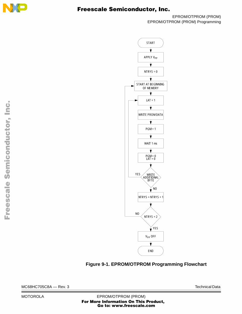
EPROM/OTPROM (PROM)EPROM/OTPROM (PROM) Programming
F
ree
sca
le S
em
ico
nd
uc
tor,
I
Freescale Semiconductor, Inc.n
c..
.
Figure 9-1. EPROM/OTPROM Programming Flowchart
YES
NO
START
APPLY VPP
NTRYS = 0
START AT BEGINNING OF MEMORY
LAT = 1
WRITE PROM DATA
PGM = 1
WAIT 1 ms
PGM = 0LAT = 0
WRITEADDITIONAL
BYTE
NTRYS = NTRYS + 1
NTRYS = 2
VPP OFF
END
YES
NO
MC68HC705C8A — Rev. 3 Technical Data
MOTOROLA EPROM/OTPROM (PROM) For More Information On This Product,
Go to: www.freescale.com
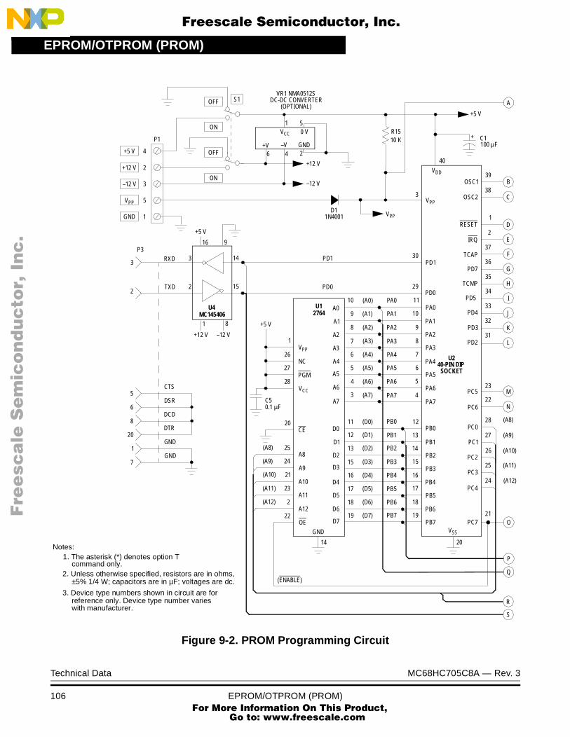
EPROM/OTPROM (PROM)
F
ree
sca
le S
em
ico
nd
uc
tor,
I
Freescale Semiconductor, Inc.n
c..
.
Figure 9-2. PROM Programming Circuit
1. The asterisk (*) denotes option T
4
2
3
5
1
1 5
6 4 2
+
3
3033
P3
1 8
2922
16 9
14
15
5
6
8
20
1
7
1
26
28
20
25
22
24
21
23
2
+12 V
OFF
ON
S1
P1
+5 V
+12 V
–12 V
VPP
GND
RXD
TXD
CTS
DSR
DCD
DTR
GND
GND
U4MC145406
+12 V –12 V
+5 V
ON
OFF
VR1 NMA0512SDC-DC CONVERTER
(OPTIONAL)
VCC 0 V
+V –V GND
–12 V
D11N4001
PD1
PD0
U12764
VPP
+5 V
NC
VCC
C50.1 µF
PGM
CE
(A10)
(A11)
(A12)
A8
A9
A10
A11
OE
GND
14
D0
10
9
8
7
6
5
4
3
(A0)
(A1)
(A2)
(A3)
(A4)
(A5)
(A6)
(A7)
11
12
13
15
16
17
18
19
R1510 K
PA0
PA1
PA2
PA3
PA4
PA5
PA6
PA7
PB0
PB1
PB2
PB3
PB4
PB5
PB6
PB7
40
VDD
VPP
PD1
PD0
PA011
10
9
8
7
6
5
4
12
13
14
15
16
17
18
19
20
VSS
PB1
PB0
PA7
PA6
PA5
PA4
PA3
PA2
U240-PIN DIP
SOCKET
PA1
+5 V
C1100 µF
OSC139
OSC238
RESET1
IRQ2
TCAP37
PD736
TCMP35
PD534
PD433
PD2
32
31
PC5
PC6
PC0
PC1
PC2
PC3
PC4
23
22
28
27
26
25
24
(A8)
(A9)
(A10)
(A11)
(A12)
PC721
M
N
L
K
J
I
H
G
F
E
D
C
B
A
(ENABLE)
(A8)
(A9) (D3)
(D2)
(D1)
(D0)
(D4)
(D5)
(D6)
(D7)O
P
Q
R
S
PD3
PB2
PB3
PB4
PB5
PB6
PB7
A0
A1
A2
A3
A4
A5
A6
A7
27
D1
D2
D3
D4
D5
D6
D7
VPP
A12
Notes:
2. Unless otherwise specified, resistors are in ohms,
3. Device type numbers shown in circuit are for
command only.
±5% 1/4 W; capacitors are in µF; voltages are dc.
reference only. Device type number varieswith manufacturer.
Technical Data MC68HC705C8A — Rev. 3
106 EPROM/OTPROM (PROM) For More Information On This Product,
Go to: www.freescale.com

EPROM/OTPROM (PROM)EPROM/OTPROM (PROM) Programming
F
ree
sca
le S
em
ico
nd
uc
tor,
I
Freescale Semiconductor, Inc.n
c..
.
Figure 9-2. PROM Programming Circuit (Continued)
123
1 2
A
B
C
D
E
F
G
H
I
J
K
L
+5 V
R10*470
DS2*
M
N
VERF
(VERF)
(PROG)
PROG
DS1*
R11*470
+5 V
O
P
Q
R
S
(D4)(D3)
(D2)
(D1)
(D0)
(A0)(A1)(A2)
(A3)(A4)
(A5)
17
1516
14
13
1211
10987
PB4PB3
PB2
PB1
PB0
PA0PA1PA2PA3PA4
PA5
C422 pF
R5
10 M
C322 pF2.0 MHz
Y1R1310 K
+5 V
+5 V
R3 10 K
R910 K
R810 K
R710 K
R610 K
PA6
PA7
V PP
NC
IRQ
RES
ET V DD
OSC
1O
SC2
TCAP N
C
PD7TCMP
PD5PD4PD3
PD2PD1PD0PC0PC1PC2
U344-LEAD PLCC
SOCKET
C60.1 µF
NC
PB5
PB6
PB7
V SS
NC
PC7
PC6
PC5
PC4
PC3
3938373635
3433323130
29
18
NC
19 20 21 22 23 24 25(P
RO
G) 26 27 28
(VER
F)
(D5)
(D6)
(D7)
NC
(A12
)(A
11)
(A10)(A9)(A8)PD0PD1
PD2
PD3PD4PD5
(A6)
6
(A7)
5 4 3
NC
2 1 44 43 42 41 40
NC
+5 V
PC7
PC6
PC5
PD0
PD1
PC4
PC3
PC2
PC1PC0
PA7
PA6
PA5
PA4
PA3
PA2
PA1
PA0
PB7
PB6
PB5
PB4
PB3
PB2
PB1
PB0
TCMP
TCAP37
35
12
13
14
15
16
17
18
19
11
10
9
8
7
6
5
4
28
27
26
25
24
30
29
23
22
21
R1210 K
PD7
PD2
PD3
PD4
PD534
33
32
31
36
S6S5S4S3
+5 V
J2
+5 VIRQ
RESET
2+5 V
R410 K
40
39
38
3
1
P2
NC
NC
NC
NC
NC
+12 V
R2
10 K
2.7 K
R1
NC
OUT1.0 µFC2 S2
J1
20VSS
MC68HC705C8A — Rev. 3 Technical Data
MOTOROLA EPROM/OTPROM (PROM) For More Information On This Product,
Go to: www.freescale.com

EPROM/OTPROM (PROM)
F
ree
sca
le S
em
ico
nd
uc
tor,
I
Freescale Semiconductor, Inc.n
c..
.
To program the PROM MCU, the MCU is installed in the PCB, along with an EPROM device programmed with user code; the MCU is then subjected to a series of routines. The routines necessary to program, verify, and secure the PROM MCU are:
• Program and verify PROM
• Verify PROM contents only
• Secure PROM and verify
• Secure PROM and dump through the serial communications interface (SCI)
Other board routines available to the user are:
• Load program into random-access memory (RAM) and execute
• Execute program in RAM
• Dump PROM contents (binary upload)
The user first configures the MCU for the bootstrap mode of operations by installing a fabricated jumper across pins 1 and 2 of the board’s mode select header, J1. Next, the board’s mode switches (S3, S4, S5, and S6) are set to determine the routine to be executed after the next reset, as shown in Table 9-2.
Table 9-2. PROM Programming Routines
Routine S3 S4 S5 S6
Program and verify PROM Off Off Off Off
Verify PROM contents only Off Off On Off
Secure PROM contents and verify On Off On Off
Secure PROM contents and dump On On On Off
Load program into RAM and execute Off On Off Off
Execute program in RAM Off Off Off On
Dump PROM contents Off On On Off
Technical Data MC68HC705C8A — Rev. 3
108 EPROM/OTPROM (PROM) For More Information On This Product,
Go to: www.freescale.com

EPROM/OTPROM (PROM)EPROM/OTPROM (PROM) Programming
F
ree
sca
le S
em
ico
nd
uc
tor,
I
Freescale Semiconductor, Inc.n
c..
.
9.3.1 Program Register
The program register (PROG) shown in Figure 9-3 is used for PROM programming.
LAT — Latch Enable Bit
This bit is both readable and writable.1 = Enables PROM data and address bus latches for programming
on the next byte write cycle0 = Latch disabled. PROM data and address buses are unlatched
for normal CPU operations.
PGM — Program Bit
If LAT is cleared, PGM cannot be set. 1 = Enables VPP power to the PROM for programming
0 = VPP is disabled.
Bits 1 and 3−7 — Not used; always read 0
Address: $001C
Bit 7 6 5 4 3 2 1 Bit 0
Read:0 0 0 0 0 LAT 0 PGM
Write:
Reset: 0 0 0 0 0 0 0 0
Figure 9-3. Program Register (PROG)
MC68HC705C8A — Rev. 3 Technical Data
MOTOROLA EPROM/OTPROM (PROM) For More Information On This Product,
Go to: www.freescale.com
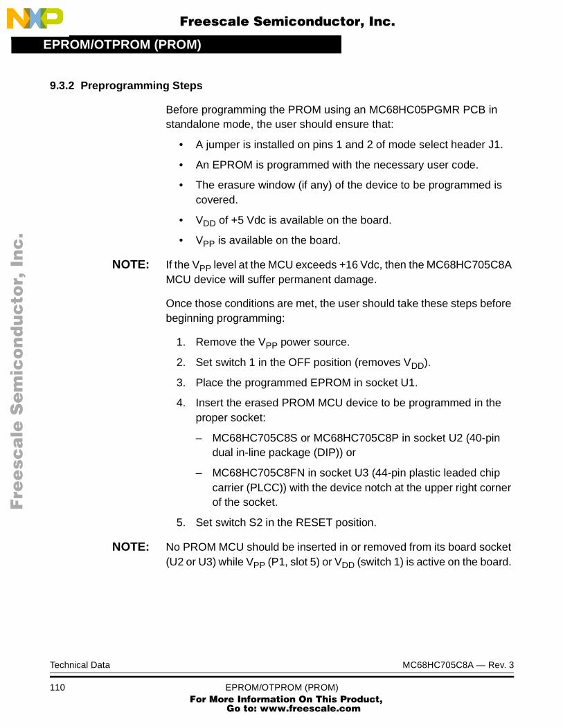
EPROM/OTPROM (PROM)
F
ree
sca
le S
em
ico
nd
uc
tor,
I
Freescale Semiconductor, Inc.n
c..
.
9.3.2 Preprogramming Steps
Before programming the PROM using an MC68HC05PGMR PCB in standalone mode, the user should ensure that:
• A jumper is installed on pins 1 and 2 of mode select header J1.
• An EPROM is programmed with the necessary user code.
• The erasure window (if any) of the device to be programmed is covered.
• VDD of +5 Vdc is available on the board.
• VPP is available on the board.
NOTE: If the VPP level at the MCU exceeds +16 Vdc, then the MC68HC705C8A MCU device will suffer permanent damage.
Once those conditions are met, the user should take these steps before beginning programming:
1. Remove the VPP power source.
2. Set switch 1 in the OFF position (removes VDD).
3. Place the programmed EPROM in socket U1.
4. Insert the erased PROM MCU device to be programmed in the proper socket:
– MC68HC705C8S or MC68HC705C8P in socket U2 (40-pin dual in-line package (DIP)) or
– MC68HC705C8FN in socket U3 (44-pin plastic leaded chip carrier (PLCC)) with the device notch at the upper right corner of the socket.
5. Set switch S2 in the RESET position.
NOTE: No PROM MCU should be inserted in or removed from its board socket (U2 or U3) while VPP (P1, slot 5) or VDD (switch 1) is active on the board.
Technical Data MC68HC705C8A — Rev. 3
110 EPROM/OTPROM (PROM) For More Information On This Product,
Go to: www.freescale.com

EPROM/OTPROM (PROM)PROM Programming Routines
F
ree
sca
le S
em
ico
nd
uc
tor,
I
Freescale Semiconductor, Inc.n
c..
.
9.4 PROM Programming Routines
This subsection describes the routines necessary to program, verify, and secure the PROM device, and other routines available to the user.
9.4.1 Program and Verify PROM
The program and verify PROM routine copies the contents of the external EPROM into the MCU PROM with direct correspondence between the addresses. Memory addresses in the MCU that are not implemented in PROM are skipped. Unprogrammed addresses in the EPROM being copied should contain $00 bytes to speed up the programming process.
To run the program and verify the PROM routine on the PROM MCU, take these steps:
1. Set switch 1 in the ON position (restores VDD).
2. Restore the VPP power source.
3. Set switches S3, S4, S5, and S6 in the OFF position (selects proper routine).
4. Set switch 2 in the OUT position (routine is activated).
The red light-emitting diode (LED) is illuminated, showing that the programming part of the routine is running. The LED goes out when programming is finished. The verification part of the routine now begins. When the green LED is illuminated, verification is successfully completed and the routine is finished.
5. Set switch 2 in the RESET position.
At this point, if no other MCU is to be programmed or secured, remove VPP power from the board. If another routine is to be performed on the MCU being programmed, the user can then set switches S3, S4, S5, and S6 to the positions necessary to select the next routine, and begin the routine by setting switch 2 to the OUT position. If no other routine is to be performed, remove VDD from the board and remove the MCU from the programming socket.
MC68HC705C8A — Rev. 3 Technical Data
MOTOROLA EPROM/OTPROM (PROM) For More Information On This Product,
Go to: www.freescale.com

EPROM/OTPROM (PROM)
F
ree
sca
le S
em
ico
nd
uc
tor,
I
Freescale Semiconductor, Inc.n
c..
.
9.4.2 Verify PROM Contents
The verify PROM contents routine is normally run automatically after the PROM is programmed. Direct entry to this routine causes the PROM contents of the MCU to be compared to the contents of the external memory locations of the EPROM at the same addresses.
To invoke the verify PROM contents routine of the MCU, take these steps:
1. Set switch 1 in the ON position (restores VDD).
2. Connect VPP to VDD.
3. Set switches S3, S4, and S6 in the OFF position.
4. Set S5 in the ON position.
5. Set switch 2 in the OUT position (routine is activated).
The red LED is not illuminated during this routine, since no programming takes place. If verification fails, the routine halts with the failing address in the external memory bus. When the green LED is illuminated, verification is completed successfully and the routine is finished.
6. Set switch 2 in the RESET position.
At this point, if another routine is to be performed on the MCU being programmed, the user can set switches S3, S4, S5, and S6 to the positions necessary to select the next routine and move switch S2 to the OUT position to start the routine. If no other routine is to be performed, remove VDD from the board and remove the MCU from the programming socket.
9.4.3 Secure PROM
The secure PROM routines are used after the PROM is successfully programmed and verified. Only the SEC bit of the option register ($1FDF) is programmed, but VPP is necessary. Once this bit is programmed, PROM is secure and can be neither verified nor dumped.
Technical Data MC68HC705C8A — Rev. 3
112 EPROM/OTPROM (PROM) For More Information On This Product,
Go to: www.freescale.com

EPROM/OTPROM (PROM)PROM Programming Routines
F
ree
sca
le S
em
ico
nd
uc
tor,
I
Freescale Semiconductor, Inc.n
c..
.
9.4.4 Secure PROM and Verify
This routine is used after the PROM is programmed successfully to verify the contents of the MCU PROM against the contents of the EPROM and then to secure the PROM. To accomplish this routine, take these steps:
1. Set switch 1 in the ON position (restores VDD).
2. Restore VPP power to the programming board.
3. Set switches S4 and S6 in the OFF position.
4. Set switches S3 and S5 in the ON position.
5. Set switch 2 in the OUT position (routine is activated). Execution time for this routine is about one second.
6. Set switch 2 in the RESET position when the routine is completed.
No LED is illuminated during this routine. Further, the end of the routine does not mean that the SEC bit was verified. To ensure that security is properly enabled, attempt to perform another verify routine. If the green LED does not light, the PROM has been secured properly.
9.4.5 Secure PROM and Dump
This routine is used after the PROM is successfully programmed to dump the contents of the MCU PROM through the SCI (binary upload) and then to secure the PROM. To accomplish this routine, take these steps:
1. Set switch 1 in the ON position (restores VDD).
2. Restore VPP power to the programming board.
3. Set switch S6 in the OFF position.
4. Set switches S3, S4, and S5 in the ON position.
5. Set switch 2 in the OUT position (routine is activated). Execution time for this routine is about one second.
6. Set switch 2 in the RESET position when the routine is completed.
MC68HC705C8A — Rev. 3 Technical Data
MOTOROLA EPROM/OTPROM (PROM) For More Information On This Product,
Go to: www.freescale.com

EPROM/OTPROM (PROM)
F
ree
sca
le S
em
ico
nd
uc
tor,
I
Freescale Semiconductor, Inc.n
c..
.
No LED is illuminated during this routine. Further, the end of the routine does not mean that the SEC bit was verified. To ensure that security is properly enabled, attempt to perform another verify routine. If the green LED does not light, the PROM has been secured properly.
9.4.6 Load Program into RAM and Execute
In the load program in RAM and execute routine, user programs are loaded via the SCI port and then executed. Data is loaded sequentially starting at address $0050. After the last byte is loaded, control is transferred to the RAM program starting at $0051. The first byte loaded is the count of the total number of bytes in the program plus the count byte. The program starts at location $0051 in RAM. During initialization, the SCI is configured for eight data bits and one stop bit. The baud rate is 4800 with a 2-MHz crystal or 9600 with a 4-MHz crystal.
To load a program into RAM and execute it, take these steps:
1. Set switch 1 in the ON position (restores VDD).
2. Connect VPP to VDD.
3. Set switches S3, S5, and S6 in the OFF position.
4. Set switch S4 in the ON position.
5. Set switch 2 in the OUT position (routine is activated).
The downloaded program starts executing as soon as the last byte is received by the SCI.
Execution of the routine can be held off by setting the byte count in the count byte (the first byte loaded) to a value greater than the number of bytes to be loaded. After loading the last byte, the firmware waits for more data. Program execution does not begin. At this point, placing switch 2 in the RESET position resets the MCU with the RAM data intact. Any other routine can be entered, including the one to execute the program in RAM, simply by setting switches S3–S6 as necessary to select the desired routine, then setting switch 2 in the OUT position.
Technical Data MC68HC705C8A — Rev. 3
114 EPROM/OTPROM (PROM) For More Information On This Product,
Go to: www.freescale.com

EPROM/OTPROM (PROM)PROM Programming Routines
F
ree
sca
le S
em
ico
nd
uc
tor,
I
Freescale Semiconductor, Inc.n
c..
.
9.4.7 Execute Program in RAM
This routine allows the MCU to transfer control to a program previously loaded in RAM. This program is executed once bootstrap mode is entered, if switch S6 is in the ON position and switch 2 is in the OUT position, without any firmware initialization. The program must start at location $0051 to be compatible with the load program in RAM routine.
To run the execute program in RAM routine, take these steps:
1. Set switch 1 in the ON position (restores VDD).
2. Connect VPP to VDD.
3. Set switch S6 in the OFF position.
4. Switches S3, S4, and S5 can be in either position.
5. Set switch 2 in the OUT position (routine is activated).
NOTE: The non-programmable watchdog COP is disabled in bootloader mode, even if the NCOPE bit is programmed.
9.4.8 Dump PROM Contents
In the dump PROM contents routine, the PROM contents are dumped sequentially to the SCI output, provided the PROM has not been secured. The first location sent is $0020 and the last location sent is $1FFF. Unused locations are skipped so that no gaps exist in the data stream. The external memory address lines indicate the current location being sent. Data is sent with eight data bits and one stop bit at 4800 baud with a 2-MHz crystal or 9600 baud with a 4-MHz crystal.
To run the dump PROM contents routine, take these steps:
1. Set switch 1 in the ON position (restores VDD).
2. Connect VPP to VDD.
3. Set switches S3 and S6 in the OFF position.
4. Set switches S4 and S5 in the ON position.
5. Set switch 2 in the OUT position (routine is activated).
6. Once PROM dumping is complete, set switch 2 in the RESET position.
MC68HC705C8A — Rev. 3 Technical Data
MOTOROLA EPROM/OTPROM (PROM) For More Information On This Product,
Go to: www.freescale.com

EPROM/OTPROM (PROM)
F
ree
sca
le S
em
ico
nd
uc
tor,
I
Freescale Semiconductor, Inc.n
c..
.
9.5 Control Registers
This subsection describes the three registers that control memory configuration, PROM security, and IRQ edge or level sensitivity; port B pullups; and non-programmable COP enable/disable.
9.5.1 Option Register
The option register shown in Figure 9-4 is used to select the IRQ sensitivity, enable the PROM security, and select the memory configuration.
RAM0 — Random-Access Memory Control Bit 0 1 = Maps 32 bytes of RAM into page zero starting at address
$0030. Addresses from $0020 to $002F are reserved. This bit can be read or written at any time, allowing memory configuration to be changed during program execution.
0 = Provides 48 bytes of PROM at location $0020–$005F.
RAM1 — Random-Access Memory Control Bit 1 1 = Maps 96 bytes of RAM into page one starting at address $0100.
This bit can be read or written at any time, allowing memory configuration to be changed during program execution.
0 = Provides 96 bytes of PROM at location $0100.
Address: $1FDF
Bit 7 6 5 4 3 2 1 Bit 0
Read:RAM0 RAM1 0 0 SEC* IRQ 0
Write:
Reset: 0 0 0 0 * U 1 0
*Implemented as an EPROM cell
= Unimplemented U = Unaffected
Figure 9-4. Option Register (Option)
Technical Data MC68HC705C8A — Rev. 3
116 EPROM/OTPROM (PROM) For More Information On This Product,
Go to: www.freescale.com

EPROM/OTPROM (PROM)Control Registers
F
ree
sca
le S
em
ico
nd
uc
tor,
I
Freescale Semiconductor, Inc.n
c..
.
SEC — Security Bit
This bit is implemented as an EPROM cell and is not affected by reset.
1 = Security enabled 0 = Security off; bootloader able to be enabled
IRQ — Interrupt Request Pin Sensitivity Bit
IRQ is set only by reset, but can be cleared by software. This bit can only be written once.
1 = IRQ pin is both negative edge- and level-sensitive. 0 = IRQ pin is negative edge-sensitive only.
Bits 5, 4, and 0 — Not used; always read 0
Bit 2 — Unaffected by reset; reads either 1 or 0
9.5.2 Mask Option Register 1
Mask option register 1 (MOR1) shown in Figure 9-5 is an EPROM register that enables the port B pullup devices. Data from MOR1 is latched on the rising edge of the voltage on the RESET pin. See 4.3.3 Port B Interrupts.
PBPU7–PBPU0/COPC — Port B Pullup Enable Bits 7–0
These EPROM bits enable the port B pullup devices.1 = Port B pullups enabled0 = Port B pullups disabled
Address: $1FF0
Bit 7 6 5 4 3 2 1 Bit 0
Read:PBPU7 PBPU6 PBPU5 PBPU4 PBPU3 PBPU2 PBPU1
PBPU0/COPCWrite:
Reset: Unaffected by reset
Erased: 0 0 0 0 0 0 0 0
Figure 9-5. Mask Option Register 1 (MOR1)
MC68HC705C8A — Rev. 3 Technical Data
MOTOROLA EPROM/OTPROM (PROM) For More Information On This Product,
Go to: www.freescale.com

EPROM/OTPROM (PROM)
F
ree
sca
le S
em
ico
nd
uc
tor,
I
Freescale Semiconductor, Inc.n
c..
.
NOTE: PBPU0/COPC programmed to a 1 enables the port B pullup bit. This bit is also used to clear the non-programmable COP (MC68HC05C4A type). Writing to this bit to clear the COP will not affect the state of the port B pull-up (bit 0). See 5.3.3 Programmable and Non-Programmable COP Watchdog Resets.
When using the MC68HC705C8A in an MC68HC705C8 or MC68HSC705C8 application, program locations $1FF0 and $1FF1 to $00.
9.5.3 Mask Option Register 2
Mask option register 2 (MOR2) shown in Figure 9-6 is an EPROM register that enables the non-programmable COP watchdog. Data from MOR2 is latched on the rising edge of the voltage on the RESET pin. See 5.3.3 Programmable and Non-Programmable COP Watchdog Resets.
NCOPE — Non-Programmable COP Watchdog Enable Bit
This EPROM bit enables the non-programmable COP watchdog.1 = Non-programmable COP watchdog enabled0 = Non-programmable COP watchdog disabled
Address: $1FF1
Bit 7 6 5 4 3 2 1 Bit 0
Read:NCOPE
Write:
Reset: Unaffected by reset
Erased: 0 0 0 0 0 0 0 0
= Unimplemented
Figure 9-6. Mask Option Register 2 (MOR2)
Technical Data MC68HC705C8A — Rev. 3
118 EPROM/OTPROM (PROM) For More Information On This Product,
Go to: www.freescale.com

EPROM/OTPROM (PROM)EPROM Erasing
F
ree
sca
le S
em
ico
nd
uc
tor,
I
Freescale Semiconductor, Inc.n
c..
.
9.6 EPROM Erasing
The erased state of an EPROM or OTPROM byte is $00. EPROM devices can be erased by exposure to a high intensity ultraviolet (UV) light with a wave length of 2537 Å. The recommended erasure dosage (UV intensity on a given surface area x exposure time) is 15 Ws/cm2. UV lamps should be used without short-wave filters, and the EPROM device should be positioned about one inch from the UV source.
OTPROM devices are shipped in an erased state. Once programmed, they cannot be erased. Electrical erasing procedures cannot be performed on either EPROM or OTPROM devices.
MC68HC705C8A — Rev. 3 Technical Data
MOTOROLA EPROM/OTPROM (PROM) For More Information On This Product,
Go to: www.freescale.com

EPROM/OTPROM (PROM)
F
ree
sca
le S
em
ico
nd
uc
tor,
I
Freescale Semiconductor, Inc.n
c..
.
Technical Data MC68HC705C8A — Rev. 3
120 EPROM/OTPROM (PROM) For More Information On This Product,
Go to: www.freescale.com

F
ree
sca
le S
em
ico
nd
uc
tor,
IFreescale Semiconductor, Inc.
nc
...
Technical Data — MC68HC705C8A
Section 10. Serial Communications Interface (SCI)
10.1 Contents
10.2 Introduction . . . . . . . . . . . . . . . . . . . . . . . . . . . . . . . . . . . . . . .121
10.3 Features . . . . . . . . . . . . . . . . . . . . . . . . . . . . . . . . . . . . . . . . .122
10.4 SCI Data Format. . . . . . . . . . . . . . . . . . . . . . . . . . . . . . . . . . .122
10.5 SCI Operation . . . . . . . . . . . . . . . . . . . . . . . . . . . . . . . . . . . . .12310.5.1 Transmitter . . . . . . . . . . . . . . . . . . . . . . . . . . . . . . . . . . . . .12310.5.2 Receiver . . . . . . . . . . . . . . . . . . . . . . . . . . . . . . . . . . . . . . .127
10.6 SCI I/O Registers . . . . . . . . . . . . . . . . . . . . . . . . . . . . . . . . . .12910.6.1 SCI Data Register . . . . . . . . . . . . . . . . . . . . . . . . . . . . . . .12910.6.2 SCI Control Register 1 . . . . . . . . . . . . . . . . . . . . . . . . . . . .13010.6.3 SCI Control Register 2 . . . . . . . . . . . . . . . . . . . . . . . . . . . .13110.6.4 SCI Status Register . . . . . . . . . . . . . . . . . . . . . . . . . . . . . .13310.6.5 Baud Rate Register . . . . . . . . . . . . . . . . . . . . . . . . . . . . . .136
10.2 Introduction
The serial communications interface (SCI) module allows high-speed asynchronous communication with peripheral devices and other microcontroller units (MCUs).
MC68HC705C8A — Rev. 3 Technical Data
MOTOROLA Serial Communications Interface (SCI) For More Information On This Product,
Go to: www.freescale.com
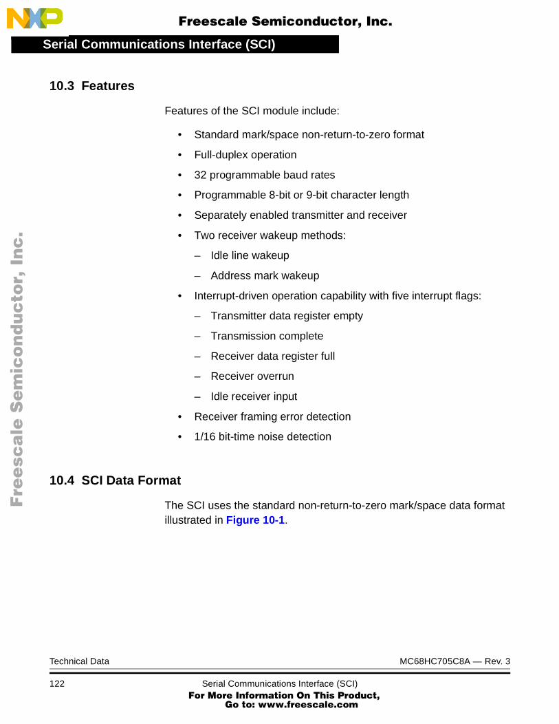
Serial Communications Interface (SCI)
F
ree
sca
le S
em
ico
nd
uc
tor,
I
Freescale Semiconductor, Inc.n
c..
.
10.3 Features
Features of the SCI module include:
• Standard mark/space non-return-to-zero format
• Full-duplex operation
• 32 programmable baud rates
• Programmable 8-bit or 9-bit character length
• Separately enabled transmitter and receiver
• Two receiver wakeup methods:
– Idle line wakeup
– Address mark wakeup
• Interrupt-driven operation capability with five interrupt flags:
– Transmitter data register empty
– Transmission complete
– Receiver data register full
– Receiver overrun
– Idle receiver input
• Receiver framing error detection
• 1/16 bit-time noise detection
10.4 SCI Data Format
The SCI uses the standard non-return-to-zero mark/space data format illustrated in Figure 10-1.
Technical Data MC68HC705C8A — Rev. 3
122 Serial Communications Interface (SCI) For More Information On This Product,
Go to: www.freescale.com
Serial Communications Interface (SCI)SCI Operation
F
ree
sca
le S
em
ico
nd
uc
tor,
I
Freescale Semiconductor, Inc.n
c..
.
Figure 10-1. SCI Data Format
10.5 SCI Operation
The SCI allows full-duplex, asynchronous, RS232 or RS422 serial communication between the MCU and remote devices, including other MCUs. The transmitter and receiver of the SCI operate independently, although they use the same baud-rate generator. This subsection describes the operation of the SCI transmitter and receiver.
10.5.1 Transmitter
Figure 10-2 shows the structure of the SCI transmitter. Figure 10-3 is a summary of the SCI transmitter input/output (I/O) registers.
• Character Length — The transmitter can accommodate either 8-bit or 9-bit data. The state of the M bit in SCI control register 1 (SCCR1) determines character length. When transmitting 9-bit data, bit T8 in SCCR1 is the ninth bit (bit 8).
• Character Transmission — During transmission, the transmit shift register shifts a character out to the PD1/TDO pin. The SCI data register (SCDR) is the write-only buffer between the internal data bus and the transmit shift register.
8-BIT DATA FORMAT(BIT M IN SCCR1 CLEAR)
9-BIT DATA FORMAT(BIT M IN SCCR1 SET)
STARTBIT BIT 0 BIT 1 BIT 2 BIT 3 BIT 4 BIT 5 BIT 6 BIT 7 BIT 8 STOP
BIT
NEXTSTART
BIT
BIT 0 BIT 1 BIT 2 BIT 3 BIT 4 BIT 5 BIT 6 BIT 7START
BITSTOPBIT
NEXTSTART
BIT
MC68HC705C8A — Rev. 3 Technical Data
MOTOROLA Serial Communications Interface (SCI) For More Information On This Product,
Go to: www.freescale.com
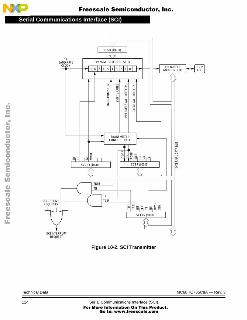
Serial Communications Interface (SCI)
F
ree
sca
le S
em
ico
nd
uc
tor,
I
Freescale Semiconductor, Inc.n
c..
.
Figure 10-2. SCI Transmitter
SCDR ($0011)
TRANSMIT SHIFT REGISTER
7 6 5 4 3 2 1 08H L
TRANSMITTERCONTROL LOGIC
LOAD
FR
OM
SC
DR
SHIF
T EN
ABLE
PREA
MBL
E (A
LL L
OG
IC 1
s)
BREA
K (A
LL L
OG
IC 0
s)
PIN BUFFERAND CONTROL
PD1/TDO
SCI RECEIVEREQUESTS
SCI INTERRUPTREQUEST
1XBAUD RATE
CLOCK
SCCR1 ($000E)
SCCR2 ($000F)
SCSR ($0010)
TIE
TCIE
RIE
ILIE
TE RE
RW
USB
K
TDR
ETC RD
RFID
LEO
RN
FFER8 T8 M W
AKE
TIE
TDRE
TC
TCIE
INTE
RNAL
DAT
A BU
S
Technical Data MC68HC705C8A — Rev. 3
124 Serial Communications Interface (SCI) For More Information On This Product,
Go to: www.freescale.com

Serial Communications Interface (SCI)SCI Operation
F
ree
sca
le S
em
ico
nd
uc
tor,
I
Freescale Semiconductor, Inc.n
c..
.
Writing a logic 1 to the TE bit in SCI control register 2 (SCCR2) and then writing data to the SCDR begins the transmission. At the start of a transmission, transmitter control logic automatically loads the transmit shift register with a preamble of logic 1s. After the preamble shifts out, the control logic transfers the SCDR data into the shift register. A logic 0 start bit automatically goes into the least significant bit (LSB) position of the shift register, and a logic 1 stop bit goes into the most significant bit (MSB) position.
When the data in the SCDR transfers to the transmit shift register, the transmit data register empty (TDRE) flag in the SCI status register (SCSR) becomes set. The TDRE flag indicates that the SCDR can accept new data from the internal data bus.
When the shift register is not transmitting a character, the PD1/TDO pin goes to the idle condition, logic 1. If software clears the TE bit during the idle condition, and while TDRE is set, the transmitter relinquishes control of the PD1/TDO pin.
Addr. Register Name Bit 7 6 5 4 3 2 1 Bit 0
$000DBaud Rate Register
(Baud)See page 136.
Read:SCP1 SCP0 SCR2 SCR1 SCR0
Write:
Reset: U U 0 0 U U U U
$000ESCI Control Register 1
(SCCR1)See page 130.
Read:R8 T8 M WAKE
Write:
Reset: U U U U
$000FSCI Control Register 2
(SCCR2)See page 131.
Read:TIE TCIE RIE ILIE TE RE RWU SBK
Write:
Reset: 0 0 0 0 0 0 0 0
$0010SCI Status Register
(SCSR)See page 133.
Read: TDRE TC RDRF IDLE OR NF FE
Write:
Reset: 1 1 0 0 0 0 0 U
$0011SCI Data Register
(SCDR)See page 129.
Read:Bit 7 Bit 6 Bit 5 Bit 4 Bit 3 Bit 2 Bit 1 Bit 0
Write:
Reset: Unaffected by reset
= Unimplemented U = Unaffected
Figure 10-3. SCI Transmitter I/O Register Summary
MC68HC705C8A — Rev. 3 Technical Data
MOTOROLA Serial Communications Interface (SCI) For More Information On This Product,
Go to: www.freescale.com

Serial Communications Interface (SCI)
F
ree
sca
le S
em
ico
nd
uc
tor,
I
Freescale Semiconductor, Inc.n
c..
.
• Break Characters — Writing a logic 1 to the SBK bit in SCCR2 loads the shift register with a break character. A break character contains all logic 0s and has no start and stop bits. Break character length depends on the M bit in SCCR1. As long as SBK is at logic 1, transmitter logic continuously loads break characters into the shift register. After software clears the SBK bit, the shift register finishes transmitting the last break character and then transmits at least one logic 1. The automatic logic 1 at the end of a break character is to guarantee the recognition of the start bit of the next character.
• Idle Characters — An idle character contains all logic 1s and has no start or stop bits. Idle character length depends on the M bit in SCCR1. The preamble is a synchronizing idle character that begins every transmission.
Clearing the TE bit during a transmission relinquishes the PD1/TDO pin after the last character to be transmitted is shifted out. The last character may already be in the shift register, or waiting in the SCDR, or it may be a break character generated by writing to the SBK bit. Toggling TE from logic 0 to logic 1 while the last character is in transmission generates an idle character (a preamble) that allows the receiver to maintain control of the PD1/TDO pin.
• Transmitter Interrupts — These sources can generate SCI transmitter interrupt requests:
– Transmit Data Register Empty (TDRE) — The TDRE bit in the SCSR indicates that the SCDR has transferred a character to the transmit shift register. TDRE is a source of SCI interrupt requests. The transmission complete interrupt enable bit (TCIE) in SCCR2 is the local mask for TDRE interrupts.
– Transmission Complete (TC) — The TC bit in the SCSR indicates that both the transmit shift register and the SCDR are empty and that no break or idle character has been generated. TC is a source of SCI interrupt requests. The transmission complete interrupt enable bit (TCIE) in SCCR2 is the local mask for TC interrupts.
Technical Data MC68HC705C8A — Rev. 3
126 Serial Communications Interface (SCI) For More Information On This Product,
Go to: www.freescale.com

Serial Communications Interface (SCI)SCI Operation
F
ree
sca
le S
em
ico
nd
uc
tor,
I
Freescale Semiconductor, Inc.n
c..
.
10.5.2 Receiver
Figure 10-4 shows the structure of the SCI receiver. Refer to Figure 10-3 for a summary of the SCI receiver I/O registers.
Figure 10-4. SCI Receiver
RECEIVE SHIFT REGISTER
7 6 5 4 3 2 1 08PIN BUFFER
AND CONTROLPD0/RDI
16XBAUD RATE
CLOCK
DATARECOVERY
STO
P
STAR
T÷16
IDLE
WAKEUPLOGIC
SCSR ($0010)
TDR
E
TC RD
RF
IDLE
OR
NF
FE
SCDR ($0011)SCCR1 ($000E)
R8 T8 M WAK
E
SCCR2 ($000F)
TIE
TCIE
RIE
ILIE
TE RE RWU
SBK
MSB RDRF OR
RDRF
RIE
IDLE
ILIE
OR
RIE
SCI TRANSMITREQUESTS
SCI INTERRUPTREQUEST
INTE
RNA
L D
ATA
BUS
REM
DISABLEDRIVER
INTE
RN
AL D
ATA
BUS
MC68HC705C8A — Rev. 3 Technical Data
MOTOROLA Serial Communications Interface (SCI) For More Information On This Product,
Go to: www.freescale.com
Serial Communications Interface (SCI)
F
ree
sca
le S
em
ico
nd
uc
tor,
I
Freescale Semiconductor, Inc.n
c..
.
• Character Length — The receiver can accommodate either 8-bit or 9-bit data. The state of the M bit in SCI control register 1 (SCCR1) determines character length. When receiving 9-bit data, bit R8 in SCCR1 is the ninth bit (bit 8).
• Character Reception — During reception, the receive shift register shifts characters in from the PD0/RDI pin. The SCI data register (SCDR) is the read-only buffer between the internal data bus and the receive shift register.
After a complete character shifts into the receive shift register, the data portion of the character is transferred to the SCDR, setting the receive data register full (RDRF) flag. The RDRF flag can be used to generate an interrupt.
• Receiver Wakeup — So that the MCU can ignore transmissions intended only for other receivers in multiple-receiver systems, the MCU can be put into a standby state. Setting the receiver wakeup enable (RWU) bit in SCI control register 2 (SCCR2) puts the MCU into a standby state during which receiver interrupts are disabled.
Either of two conditions on the PD0/RDI pin can bring the MCU out of the standby state:
– Idle input line condition — If the PD0/RDI pin is at logic 1 long enough for 10 or 11 logic 1s to shift into the receive shift register, receiver interrupts are again enabled.
– Address mark — If a logic 1 occurs in the most significant bit position of a received character, receiver interrupts are again enabled.
The state of the WAKE bit in SCCR1 determines which of the two conditions wakes up the MCU.
• Receiver Noise Immunity — The data recovery logic samples each bit 16 times to identify and verify the start bit and to detect noise. Any conflict between noise detection samples sets the noise flag (NF) in the SCSR. The NF bit is set at the same time that the RDRF bit is set.
Technical Data MC68HC705C8A — Rev. 3
128 Serial Communications Interface (SCI) For More Information On This Product,
Go to: www.freescale.com
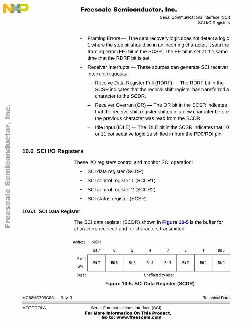
Serial Communications Interface (SCI)SCI I/O Registers
F
ree
sca
le S
em
ico
nd
uc
tor,
I
Freescale Semiconductor, Inc.n
c..
.
• Framing Errors — If the data recovery logic does not detect a logic 1 where the stop bit should be in an incoming character, it sets the framing error (FE) bit in the SCSR. The FE bit is set at the same time that the RDRF bit is set.
• Receiver Interrupts — These sources can generate SCI receiver interrupt requests:
– Receive Data Register Full (RDRF) — The RDRF bit in the SCSR indicates that the receive shift register has transferred a character to the SCDR.
– Receiver Overrun (OR) — The OR bit in the SCSR indicates that the receive shift register shifted in a new character before the previous character was read from the SCDR.
– Idle Input (IDLE) — The IDLE bit in the SCSR indicates that 10 or 11 consecutive logic 1s shifted in from the PD0/RDI pin.
10.6 SCI I/O Registers
These I/O registers control and monitor SCI operation:
• SCI data register (SCDR)
• SCI control register 1 (SCCR1)
• SCI control register 2 (SCCR2)
• SCI status register (SCSR)
10.6.1 SCI Data Register
The SCI data register (SCDR) shown in Figure 10-5 is the buffer for characters received and for characters transmitted.
Address: $0011
Bit 7 6 5 4 3 2 1 Bit 0
Read:Bit 7 Bit 6 Bit 5 Bit 4 Bit 3 Bit 2 Bit 1 Bit 0
Write:
Reset: Unaffected by reset
Figure 10-5. SCI Data Register (SCDR)
MC68HC705C8A — Rev. 3 Technical Data
MOTOROLA Serial Communications Interface (SCI) For More Information On This Product,
Go to: www.freescale.com

Serial Communications Interface (SCI)
F
ree
sca
le S
em
ico
nd
uc
tor,
I
Freescale Semiconductor, Inc.n
c..
.
10.6.2 SCI Control Register 1
SCI control register 1 (SCCR1) shown in Figure 10-6 has these functions:
• Stores ninth SCI data bit received and ninth SCI data bit transmitted
• Controls SCI character length
• Controls SCI wakeup method
R8 — Bit 8 (Received)
When the SCI is receiving 9-bit characters, R8 is the ninth bit of the received character. R8 receives the ninth bit at the same time that the SCDR receives the other eight bits. Reset has no effect on the R8 bit.
T8 — Bit 8 (Transmitted)
When the SCI is transmitting 9-bit characters, T8 is the ninth bit of the transmitted character. T8 is loaded into the transmit shift register at the same time that SCDR is loaded into the transmit shift register. Reset has no effect on the T8 bit.
M — Character Length Bit
This read/write bit determines whether SCI characters are eight or nine bits long. The ninth bit can be used as an extra stop bit, as a receiver wakeup signal, or as a mark or space parity bit. Reset has no effect on the M bit.
1 = 9-bit SCI characters0 = 8-bit SCI characters
Address: $000E
Bit 7 6 5 4 3 2 1 Bit 0
Read:R8 T8 M WAKE
Write:
Reset: U U U U
= Unimplemented U = Unaffected
Figure 10-6. SCI Control Register 1 (SCCR1)
Technical Data MC68HC705C8A — Rev. 3
130 Serial Communications Interface (SCI) For More Information On This Product,
Go to: www.freescale.com

Serial Communications Interface (SCI)SCI I/O Registers
F
ree
sca
le S
em
ico
nd
uc
tor,
I
Freescale Semiconductor, Inc.n
c..
.
WAKE — Wakeup Bit
This read/write bit determines which condition wakes up the SCI: a logic 1 (address mark) in the most significant bit position of a received character or an idle condition of the PD0/RDI pin. Reset has no effect on the WAKE bit.
1 = Address mark wakeup0 = Idle line wakeup
10.6.3 SCI Control Register 2
SCI control register 2 (SCCR2) shown in Figure 10-7 has these functions:
• Enables the SCI receiver and SCI receiver interrupts
• Enables the SCI transmitter and SCI transmitter interrupts
• Enables SCI receiver idle interrupts
• Enables SCI transmission complete interrupts
• Enables SCI wakeup
• Transmits SCI break characters
TIE — Transmit Interrupt Enable Bit
This read/write bit enables SCI interrupt requests when the TDRE bit becomes set. Reset clears the TIE bit.
1 = TDRE interrupt requests enabled0 = TDRE interrupt requests disabled
Address: $000F
Bit 7 6 5 4 3 2 1 Bit 0
Read:TIE TCIE RIE ILIE TE RE RWU SBK
Write:
Reset: 0 0 0 0 0 0 0 0
Figure 10-7. SCI Control Register 2 (SCCR2)
MC68HC705C8A — Rev. 3 Technical Data
MOTOROLA Serial Communications Interface (SCI) For More Information On This Product,
Go to: www.freescale.com

Serial Communications Interface (SCI)
F
ree
sca
le S
em
ico
nd
uc
tor,
I
Freescale Semiconductor, Inc.n
c..
.
TCIE — Transmission Complete Interrupt Enable Bit
This read/write bit enables SCI interrupt requests when the TC bit becomes set. Reset clears the TCIE bit.
1 = TC interrupt requests enabled0 = TC interrupt requests disabled
RIE — Receive Interrupt Enable Bit
This read/write bit enables SCI interrupt requests when the RDRF bit or the OR bit becomes set. Reset clears the RIE bit.
1 = RDRF interrupt requests enabled0 = RDRF interrupt requests disabled
ILIE — Idle Line Interrupt Enable Bit
This read/write bit enables SCI interrupt requests when the IDLE bit becomes set. Reset clears the ILIE bit.
1 = IDLE interrupt requests enabled0 = IDLE interrupt requests disabled
TE — Transmit Enable Bit
Setting this read/write bit begins the transmission by sending a preamble of 10 or 11 logic 1s from the transmit shift register to the PD1/TDO pin. Reset clears the TE bit.
1 = Transmission enabled0 = Transmission disabled
RE — Receive Enable Bit
Setting this read/write bit enables the receiver. Clearing the RE bit disables the receiver and receiver interrupts but does not affect the receiver interrupt flags. Reset clears the RE bit.
1 = Receiver enabled0 = Receiver disabled
RWU — Receiver Wakeup Enable Bit
This read/write bit puts the receiver in a standby state. Typically, data transmitted to the receiver clears the RWU bit and returns the receiver to normal operation. The WAKE bit in SCCR1 determines whether an
Technical Data MC68HC705C8A — Rev. 3
132 Serial Communications Interface (SCI) For More Information On This Product,
Go to: www.freescale.com

Serial Communications Interface (SCI)SCI I/O Registers
F
ree
sca
le S
em
ico
nd
uc
tor,
I
Freescale Semiconductor, Inc.n
c..
.
idle input or an address mark brings the receiver out of the standby state. Reset clears the RWU bit.
1 = Standby state0 = Normal operation
SBK — Send Break Bit
Setting this read/write bit continuously transmits break codes in the form of 10-bit or 11-bit groups of logic 0s. Clearing the SBK bit stops the break codes and transmits a logic 1 as a start bit. Reset clears the SBK bit.
1 = Break codes being transmitted0 = No break codes being transmitted
10.6.4 SCI Status Register
The SCI status register (SCSR) shown in Figure 10-8 contains flags to signal these conditions:
• Transfer of SCDR data to transmit shift register complete
• Transmission complete
• Transfer of receive shift register data to SCDR complete
• Receiver input idle
• Receiver overrun
• Noisy data
• Framing error
Address: $0010
Bit 7 6 5 4 3 2 1 Bit 0
Read: TDRE TC RDRF IDLE OR NF FE
Write:
Reset: 1 1 0 0 0 0 0 U
= Unimplemented U = Unaffected
Figure 10-8. SCI Status Register (SCSR)
MC68HC705C8A — Rev. 3 Technical Data
MOTOROLA Serial Communications Interface (SCI) For More Information On This Product,
Go to: www.freescale.com
Serial Communications Interface (SCI)
F
ree
sca
le S
em
ico
nd
uc
tor,
I
Freescale Semiconductor, Inc.n
c..
.
TDRE — Transmit Data Register Empty Bit
This clearable, read-only bit is set when the data in the SCDR transfers to the transmit shift register. TDRE generates an interrupt request if the TIE bit in SCCR2 is also set. Clear the TDRE bit by reading the SCSR with TDRE set and then writing to the SCDR. Reset sets the TDRE bit. Software must initialize the TDRE bit to logic 0 to avoid an instant interrupt request when turning on the transmitter.
1 = SCDR data transferred to transmit shift register0 = SCDR data not transferred to transmit shift register
TC — Transmission Complete Bit
This clearable, read-only bit is set when the TDRE bit is set and no data, preamble, or break character is being transmitted. TC generates an interrupt request if the TCIE bit in SCCR2 is also set. Clear the TC bit by reading the SCSR with TC set and then writing to the SCDR. Reset sets the TC bit. Software must initialize the TC bit to logic 0 to avoid an instant interrupt request when turning on the transmitter.
1 = No transmission in progress0 = Transmission in progress
RDRF — Receive Data Register Full Bit
This clearable, read-only bit is set when the data in the receive shift register transfers to the SCI data register. RDRF generates an interrupt request if the RIE bit in SCCR2 is also set. Clear the RDRF bit by reading the SCSR with RDRF set and then reading the SCDR. Reset clears the RDRF bit.
1 = Received data available in SCDR0 = Received data not available in SCDR
IDLE — Receiver Idle Bit
This clearable, read-only bit is set when 10 or 11 consecutive logic 1s appear on the receiver input. IDLE generates an interrupt request if the ILIE bit in SCCR2 is also set. Clear the IDLE bit by reading the SCSR with IDLE set, and then reading the SCDR. Reset clears the IDLE bit.
1 = Receiver input idle0 = Receiver input not idle
Technical Data MC68HC705C8A — Rev. 3
134 Serial Communications Interface (SCI) For More Information On This Product,
Go to: www.freescale.com

Serial Communications Interface (SCI)SCI I/O Registers
F
ree
sca
le S
em
ico
nd
uc
tor,
I
Freescale Semiconductor, Inc.n
c..
.
OR — Receiver Overrun Bit
This clearable, read-only bit is set if the SCDR is not read before the receive shift register receives the next word. OR generates an interrupt request if the RIE bit in SCCR2 is also set. The data in the shift register is lost, but the data already in the SCDR is not affected. Clear the OR bit by reading the SCSR with OR set and then reading the SCDR. Reset clears the OR bit.
1 = Receiver shift register full and RDRF = 10 = No receiver overrun
NF — Receiver Noise Flag Bit
This clearable, read-only bit is set when noise is detected in data received in the SCI data register. Clear the NF bit by reading the SCSR and then reading the SCDR. Reset clears the NF bit.
1 = Noise detected in SCDR0 = No noise detected in SCDR
FE — Receiver Framing Error Bit
This clearable, read-only flag is set when a logic 0 is located where a stop bit should be in the character shifted into the receive shift register. If the received word causes both a framing error and an overrun error, the OR bit is set and the FE bit is not set. Clear the FE bit by reading the SCSR and then reading the SCDR. Reset clears the FE bit.
1 = Framing error0 = No framing error
MC68HC705C8A — Rev. 3 Technical Data
MOTOROLA Serial Communications Interface (SCI) For More Information On This Product,
Go to: www.freescale.com

Serial Communications Interface (SCI)
F
ree
sca
le S
em
ico
nd
uc
tor,
I
Freescale Semiconductor, Inc.n
c..
.
10.6.5 Baud Rate Register
The baud rate register shown in Figure 10-9 selects the baud rate for both the receiver and the transmitter.
SCP1 and SCP0 — SCI Prescaler Select Bits
These read/write bits control prescaling of the baud rate generator clock, as shown in Table 10-1. Resets clear both SCP1 and SCP0.
Address: $000D
Bit 7 6 5 4 3 2 1 Bit 0
Read:SCP1 SCP0 SCR2 SCR1 SCR0
Write:
Reset: U U 0 0 U U U U
= Unimplemented U = Unaffected
Figure 10-9. Baud Rate Register (Baud)
Table 10-1. Baud Rate Generator Clock Prescaling
SCP[1:0] Baud Rate Generator Clock
00 Internal clock ÷ 1
01 Internal clock ÷ 3
10 Internal clock ÷ 4
11 Internal clock ÷ 13
Technical Data MC68HC705C8A — Rev. 3
136 Serial Communications Interface (SCI) For More Information On This Product,
Go to: www.freescale.com

Serial Communications Interface (SCI)SCI I/O Registers
F
ree
sca
le S
em
ico
nd
uc
tor,
I
Freescale Semiconductor, Inc.n
c..
.
SCR2–SCR0 — SCI Baud Rate Select BitsThese read/write bits select the SCI baud rate, as shown in Table 10-2. Reset has no effect on the SCR2–SCR0 bits.
Table 10-3 shows all possible SCI baud rates derived from crystal frequencies of 2 MHz, 4 MHz, and 4.194304 MHz.
Table 10-2. Baud Rate Selection
SCR[2:1:0] SCI Baud Rate (Baud)
000 Prescaled clock ÷ 1
001 Prescaled clock ÷ 2
010 Prescaled clock ÷ 4
011 Prescaled clock ÷ 8
100 Prescaled clock ÷ 16
101 Prescaled clock ÷ 32
110 Prescaled clock ÷ 64
111 Prescaled clock ÷ 128
MC68HC705C8A — Rev. 3 Technical Data
MOTOROLA Serial Communications Interface (SCI) For More Information On This Product,
Go to: www.freescale.com

Serial Communications Interface (SCI)
F
ree
sca
le S
em
ico
nd
uc
tor,
I
Freescale Semiconductor, Inc.n
c..
.
Table 10-3. Baud Rate Selection Examples
SCP[1:0] SCR[2:1:0]SCI Baud Rate
fOSC = 2 MHz fOSC = 4 MHz fOSC = 4.194304 MHz
00 000 62.50 Kbaud 125 Kbaud 131.1 Kbaud
00 001 31.25 Kbaud 62.50 Kbaud 65.54 Kbaud
00 010 15.63 Kbaud 31.25 Kbaud 32.77 Kbaud
00 011 7813 baud 15.63 Kbaud 16.38 Kbaud
00 100 3906 baud 7813 baud 8192 baud
00 101 1953 baud 3906 baud 4096 baud
00 110 976.6 baud 1953 baud 2048 baud
00 111 488.3 baud 976.6 baud 1024 baud
01 000 20.83 Kbaud 41.67 Kbaud 43.69 Kbaud
01 001 10.42 Kbaud 20.83 Kbaud 21.85 Kbaud
01 010 5208 baud 10.42 Kbaud 10.92 Kbaud
01 011 2604 baud 5208 baud 5461 baud
01 100 1302 baud 2604 baud 2731 baud
01 101 651.0 baud 1302 baud 1365 baud
01 110 325.5 baud 651.0 baud 682.7 baud
01 111 162.8 baud 325.5 baud 341.3 baud
10 000 15.63 Kbaud 31.25 Kbaud 32.77 Kbaud
10 001 7813 baud 15.63 Kbaud 16.38 Kbaud
10 010 3906 baud 7813 baud 8192 baud
10 011 1953 baud 3906 baud 4906 baud
10 100 976.6 baud 1953 baud 2048 baud
10 101 488.3 baud 976.6 baud 1024 baud
10 110 244.1 baud 488.3 baud 512.0 baud
10 111 122.1 baud 244.1 baud 256.0 baud
11 000 4808 baud 9615 baud 10.08 Kbaud
11 001 2404 baud 4808 baud 5041 baud
11 010 1202 baud 2404 baud 2521 baud
11 011 601.0 baud 1202 baud 1260 baud
11 100 300.5 baud 601.0 baud 630.2 baud
11 101 150.2 baud 300.5 baud 315.1 baud
11 110 75.12 baud 150.2 baud 157.5 baud
11 111 37.56 baud 75.12 baud 78.77 baud
Technical Data MC68HC705C8A — Rev. 3
138 Serial Communications Interface (SCI) For More Information On This Product,
Go to: www.freescale.com
F
ree
sca
le S
em
ico
nd
uc
tor,
IFreescale Semiconductor, Inc.
nc
...
Technical Data — MC68HC705C8A
Section 11. Serial Peripheral Interface (SPI)
11.1 Contents
11.2 Introduction . . . . . . . . . . . . . . . . . . . . . . . . . . . . . . . . . . . . . . .139
11.3 Features . . . . . . . . . . . . . . . . . . . . . . . . . . . . . . . . . . . . . . . . .140
11.4 Operation . . . . . . . . . . . . . . . . . . . . . . . . . . . . . . . . . . . . . . . .14211.4.1 Pin Functions in Master Mode . . . . . . . . . . . . . . . . . . . . . .14311.4.2 Pin Functions in Slave Mode . . . . . . . . . . . . . . . . . . . . . . .144
11.5 Multiple-SPI Systems . . . . . . . . . . . . . . . . . . . . . . . . . . . . . . .145
11.6 Serial Clock Polarity and Phase . . . . . . . . . . . . . . . . . . . . . . .146
11.7 SPI Error Conditions . . . . . . . . . . . . . . . . . . . . . . . . . . . . . . . .14711.7.1 Mode Fault Error . . . . . . . . . . . . . . . . . . . . . . . . . . . . . . . .14711.7.2 Write Collision Error . . . . . . . . . . . . . . . . . . . . . . . . . . . . . .14711.7.3 Overrun Error . . . . . . . . . . . . . . . . . . . . . . . . . . . . . . . . . . .148
11.8 SPI Interrupts . . . . . . . . . . . . . . . . . . . . . . . . . . . . . . . . . . . . .148
11.9 SPI I/O Registers . . . . . . . . . . . . . . . . . . . . . . . . . . . . . . . . . .14811.9.1 SPI Data Register. . . . . . . . . . . . . . . . . . . . . . . . . . . . . . . .14911.9.2 SPI Control Register. . . . . . . . . . . . . . . . . . . . . . . . . . . . . .14911.9.3 SPI Status Register . . . . . . . . . . . . . . . . . . . . . . . . . . . . . .151
11.2 Introduction
The serial peripheral interface (SPI) module allows full-duplex, synchronous, serial communication with peripheral devices.
MC68HC705C8A — Rev. 3 Technical Data
MOTOROLA Serial Peripheral Interface (SPI) For More Information On This Product,
Go to: www.freescale.com
Serial Peripheral Interface (SPI)
F
ree
sca
le S
em
ico
nd
uc
tor,
I
Freescale Semiconductor, Inc.n
c..
.
11.3 Features
Features of the SPI include:
• Full-duplex operation
• Master and slave modes
• Four programmable master mode frequencies (1.05 MHz maximum)
• 2.1-MHz maximum slave mode frequency
• Serial clock with programmable polarity and phase
• End of transmission interrupt flag
• Write collision error flag
• Bus contention error flag
Figure 11-1 shows the structure of the SPI module. Figure 11-2 is a summary of the SPI input/output (I/O) registers.
Technical Data MC68HC705C8A — Rev. 3
140 Serial Peripheral Interface (SPI) For More Information On This Product,
Go to: www.freescale.com

Serial Peripheral Interface (SPI)Features
F
ree
sca
le S
em
ico
nd
uc
tor,
I
Freescale Semiconductor, Inc.n
c..
.
Figure 11-1. SPI Block Diagram
SPI SHIFT REGISTER
DIVIDER
SPCR ($000A)
7 6 5 4 3 2 1 0
PD4/SCK
PD3/MOSI
÷2 ÷32÷6÷4
SELECT
SPI CONTROL
S
M
M
S
INTERNALCLOCK
(XTAL ÷2)
PIN
CO
NTR
OL
LOG
IC
PD2/MISO
SPSR ($000B)
SPIF
WC
OL
MO
DF
REQUEST
SPR
1
SPR0
SPDR ($000C)
SPI INTERRUPT INTERNALDATA BUS
SPI CLOCK (MASTER)
CLOCKLOGIC
MSTRSPE
M
S
MSTRSPEDWOM
SPIE
SPE
DW
OM
MST
R
CPH
A
CPO
L
SPR
1
SPR
0
SHIFT CLOCK
SPIE
PD5/SS
MC68HC705C8A — Rev. 3 Technical Data
MOTOROLA Serial Peripheral Interface (SPI) For More Information On This Product,
Go to: www.freescale.com
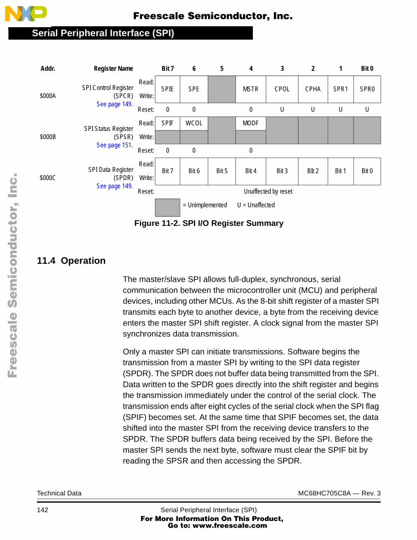
Serial Peripheral Interface (SPI)
F
ree
sca
le S
em
ico
nd
uc
tor,
I
Freescale Semiconductor, Inc.n
c..
.
11.4 Operation
The master/slave SPI allows full-duplex, synchronous, serial communication between the microcontroller unit (MCU) and peripheral devices, including other MCUs. As the 8-bit shift register of a master SPI transmits each byte to another device, a byte from the receiving device enters the master SPI shift register. A clock signal from the master SPI synchronizes data transmission.
Only a master SPI can initiate transmissions. Software begins the transmission from a master SPI by writing to the SPI data register (SPDR). The SPDR does not buffer data being transmitted from the SPI. Data written to the SPDR goes directly into the shift register and begins the transmission immediately under the control of the serial clock. The transmission ends after eight cycles of the serial clock when the SPI flag (SPIF) becomes set. At the same time that SPIF becomes set, the data shifted into the master SPI from the receiving device transfers to the SPDR. The SPDR buffers data being received by the SPI. Before the master SPI sends the next byte, software must clear the SPIF bit by reading the SPSR and then accessing the SPDR.
Addr. Register Name Bit 7 6 5 4 3 2 1 Bit 0
$000ASPI Control Register
(SPCR)See page 149.
Read:SPIE SPE MSTR CPOL CPHA SPR1 SPR0
Write:
Reset: 0 0 0 U U U U
$000BSPI Status Register
(SPSR)See page 151.
Read: SPIF WCOL MODF
Write:
Reset: 0 0 0
$000CSPI Data Register
(SPDR)See page 149.
Read:Bit 7 Bit 6 Bit 5 Bit 4 Bit 3 BIt 2 Bit 1 Bit 0
Write:
Reset: Unaffected by reset
= Unimplemented U = Unaffected
Figure 11-2. SPI I/O Register Summary
Technical Data MC68HC705C8A — Rev. 3
142 Serial Peripheral Interface (SPI) For More Information On This Product,
Go to: www.freescale.com

Serial Peripheral Interface (SPI)Operation
F
ree
sca
le S
em
ico
nd
uc
tor,
I
Freescale Semiconductor, Inc.n
c..
.
In a slave SPI, data enters the shift register under the control of the serial clock from the master SPI. After a byte enters the shift register of a slave SPI, it transfers to the SPDR. To prevent an overrun condition, slave software must then read the byte in the SPDR before another byte enters the shift register and is ready to transfer to the SPDR.
Figure 11-3 shows how a master SPI exchanges data with a slave SPI.
Figure 11-3. Master/Slave Connections
11.4.1 Pin Functions in Master Mode
Setting the MSTR bit in the SPI control register (SPCR) configures the SPI for operation in master mode. The master-mode functions of the SPI pins are:
• PD4/SCK (serial clock) — In master mode, the PD4/SCK pin is the synchronizing clock output.
• PD3/MOSI (master output, slave input) — In master mode, the PD3/MOSI pin is the serial output.
• PD2/MISO (master input, slave output) — In master mode, the PD2/MISO pin is configured as the serial input.
• PD5/SS (slave select) — In master mode, the PD5/SS pin protects against driver contention caused by the simultaneous operation of two SPIs in master mode. A logic 0 on the PD5/SS pin of a master SPI disables the SPI, clears the MSTR bit, and sets the mode-fault flag (MODF).
SPI SHIFT REGISTER
7 6 5 4 3 2 1 0
SPI SHIFT REGISTER
7 6 5 4 3 2 1 0
SPDR ($000C) SPDR ($000C)
PD3/MOSI
PD2/MISO
PD5/SS
PD4/SCK
MASTER MCU SLAVE MCU
MC68HC705C8A — Rev. 3 Technical Data
MOTOROLA Serial Peripheral Interface (SPI) For More Information On This Product,
Go to: www.freescale.com

Serial Peripheral Interface (SPI)
F
ree
sca
le S
em
ico
nd
uc
tor,
I
Freescale Semiconductor, Inc.n
c..
.
11.4.2 Pin Functions in Slave Mode
Clearing the MSTR bit in the SPCR configures the SPI for operation in slave mode. The slave-mode functions of the SPI pins are:
• PD4/SCK (serial clock) — In slave mode, the PD4/SCK pin is the input for the synchronizing clock signal from the master SPI.
• PD3/MOSI (master output, slave input) — In slave mode, the PD3/MOSI pin is the serial input.
• PD2/MISO (master input, slave output) — In slave mode, the PD2/MISO pin is the serial output.
• PD5/SS (slave select) — In slave mode, the PD5/SS pin enables the SPI for data and serial clock reception from a master SPI.
When CPHA = 0, the shift clock is the OR of SS with SCK. In this clock phase mode, SS must go high between successive characters in an SPI message. When CPHA = 1, SS may be left low for several SPI characters. In cases with only one SPI slave MCU, the slave MCU SS line can be tied to VSS as long as CPHA = 1 clock modes are used.
The WCOL flag bit can be improperly set when attempting the first transmission after a reset if these conditions are present: MSTR = 0, CPOL = 0, CPHA = 1, SS pin = 0, and SCK pin = 1. The reset states of the CPOL and CPHA bits are 0 and 1, respectively. Under normal operating conditions (CPOL = 0, CPHA = 1), the SCK input will be low.
The incorrect setting of the WCOL bit can be prevented in two ways:
1. Send a dummy transmission after reset, clear the WCOL flag, and then proceed with the real transmission.
2. Use the MSTR bit in the SPCR (SPI control register). This is accomplished by setting the MSTR bit at the same time the CPOL and CPHA bits are programmed to the desired logic levels. Then, the data register can be written to if desired. After this, the MSTR bit should be set to a logic 0, the SPE (SPI enable bit) should be set to a logic 1, and the CPOL, CPHA, SPR1, and SPR0 bits set to the desired logic levels. If this procedure is followed after a reset and before the first access to the SPDR, the WCOL flag will not be set.
Technical Data MC68HC705C8A — Rev. 3
144 Serial Peripheral Interface (SPI) For More Information On This Product,
Go to: www.freescale.com
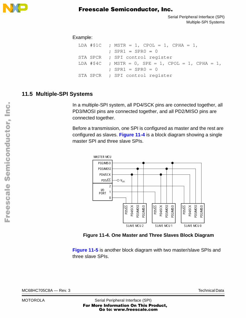
Serial Peripheral Interface (SPI)Multiple-SPI Systems
F
ree
sca
le S
em
ico
nd
uc
tor,
I
Freescale Semiconductor, Inc.n
c..
.
Example:
LDA #$1C ; MSTR = 1, CPOL = 1, CPHA = 1, ; SPR1 = SPR0 = 0
STA SPCR ; SPI control registerLDA #$4C ; MSTR = 0, SPE = 1, CPOL = 1, CPHA = 1,
; SPR1 = SPR0 = 0STA SPCR ; SPI control register
11.5 Multiple-SPI Systems
In a multiple-SPI system, all PD4/SCK pins are connected together, all PD3/MOSI pins are connected together, and all PD2/MISO pins are connected together.
Before a transmission, one SPI is configured as master and the rest are configured as slaves. Figure 11-4 is a block diagram showing a single master SPI and three slave SPIs.
Figure 11-4. One Master and Three Slaves Block Diagram
Figure 11-5 is another block diagram with two master/slave SPIs and three slave SPIs.
PD2/MISO
PD3/MOSI
PD4/SCK
PD5/SS
I/O2
1
0
SLAVE MCU 2 SLAVE MCU 1 SLAVE MCU 0
PD5/
SS
PD4/
SCK
PD3/
MO
SI
PD2/
MIS
O
MASTER MCU
PORT
PD5/
SS
PD4/
SCK
PD3/
MO
SI
PD2/
MIS
O
PD5/
SS
PD4/
SCK
PD3/
MO
SI
PD2/
MIS
O
VDD
MC68HC705C8A — Rev. 3 Technical Data
MOTOROLA Serial Peripheral Interface (SPI) For More Information On This Product,
Go to: www.freescale.com

Serial Peripheral Interface (SPI)
F
ree
sca
le S
em
ico
nd
uc
tor,
I
Freescale Semiconductor, Inc.n
c..
.
Figure 11-5. Two Master/Slaves and Three Slaves Block Diagram
11.6 Serial Clock Polarity and Phase
To accommodate the different serial communication requirements of peripheral devices, software can change the phase and polarity of the SPI serial clock. The clock polarity bit (CPOL) and the clock phase bit (CPHA), both in the SPCR, control the timing relationship between the serial clock and the transmitted data. Figure 11-6 shows how the CPOL and CPHA bits affect the clock/data timing.
Figure 11-6. SPI Clock/Data Timing
SLAVE MCU 2 SLAVE MCU 1 SLAVE MCU 0
PD5/
SS
PD4/
SCK
PD3/
MO
SI
PD2/
MIS
O
MASTER/SLAVE
PD5/
SS
PD4/
SCK
PD3/
MO
SI
PD2/
MIS
O
PD5/
SS
PD4/
SCK
PD3/
MO
SI
PD2/
MIS
O
PD2/MISO
PD3/MOSI
PD4/SCK
PD5/SS
I/O
0
1
2 PORT
3
PD2/MISO
PD3/MOSI
PD4/SCK
PD5/SS
I/O
0
1
2PORT
3
MCU 1MASTER/SLAVE
MCU 2
MSB BIT 6 BIT 5 BIT 4 BIT 3 BIT 2 BIT 1 LSBSDO/SDI
1
0
1
0
SS
1
1
0
0
SCK (D)
SCK (C)
SCK (B)
SCK (A)
CPHA CPOL
CAPTURE STROBE
Technical Data MC68HC705C8A — Rev. 3
146 Serial Peripheral Interface (SPI) For More Information On This Product,
Go to: www.freescale.com

Serial Peripheral Interface (SPI)SPI Error Conditions
F
ree
sca
le S
em
ico
nd
uc
tor,
I
Freescale Semiconductor, Inc.n
c..
.
11.7 SPI Error Conditions
These conditions produce SPI system errors:
• Bus contention caused by multiple master SPIs (mode fault error)
• Writing to the SPDR during a transmission (write-collision error)
• Failing to read the SPDR before the next incoming byte sets the SPIF bit (overrun error)
11.7.1 Mode Fault Error
A mode fault error results when a logic 0 occurs on the PD5/SS pin of a master SPI. The MCU takes these actions when a mode fault error occurs:
• Puts the SPI in slave mode by clearing the MSTR bit
• Disables the SPI by clearing the SPE bit
• Sets the MODF bit
11.7.2 Write Collision Error
Writing to the SPDR during a transmission causes a write collision error and sets the WCOL bit in the SPSR. Either a master SPI or a slave SPI can generate a write collision error.
• Master — A master SPI can cause a write collision error by writing to the SPDR while the previously written byte is still being shifted out to the PD3/MOSI pin. The error does not affect the transmission of the previously written byte, but the byte that caused the error is lost.
• Slave — A slave SPI can cause a write collision error in either of two ways, depending on the state of the CPHA bit:
– CPHA = 0 — A slave SPI can cause a write collision error by writing to the SPDR while the PD5/SS pin is at logic 0. The error does not affect the byte in the SPDR, but the byte that caused the error is lost.
MC68HC705C8A — Rev. 3 Technical Data
MOTOROLA Serial Peripheral Interface (SPI) For More Information On This Product,
Go to: www.freescale.com

Serial Peripheral Interface (SPI)
F
ree
sca
le S
em
ico
nd
uc
tor,
I
Freescale Semiconductor, Inc.n
c..
.
– CPHA = 1 — A slave SPI can cause a write collision error by writing to the SPDR while receiving a transmission, that is, between the first active SCK edge and the end of the eighth SCK cycle. The error does not affect the transmission from the master SPI, but the byte that caused the error is lost.
11.7.3 Overrun Error
Failing to read the byte in the SPDR before a subsequent byte enters the shift register causes an overrun condition. In an overrun condition, all incoming data is lost until software clears SPIF. The overrun condition has no flag.
11.8 SPI Interrupts
The SPIF bit in the SPSR indicates a byte has shifted into or out of the SPDR. The SPIF bit is a source of SPI interrupt requests. The SPI interrupt enable bit (SPIE) in the SPCR is the local mask for SPIF interrupts.
The MODF bit in the SPSR indicates a mode error and is a source of SPI interrupt requests. The MODF bit is set when a logic 0 occurs on the PD5/SS pin while the MSTR bit is set. The SPI interrupt enable bit (SPIE) in the SPCR is the local mask for MODF interrupts.
11.9 SPI I/O Registers
These input/output (I/O) registers control and monitor SPI operation:
• SPI data register (SPDR)
• SPI control register (SPCR)
• SPI status register (SPSR)
Technical Data MC68HC705C8A — Rev. 3
148 Serial Peripheral Interface (SPI) For More Information On This Product,
Go to: www.freescale.com

Serial Peripheral Interface (SPI)SPI I/O Registers
F
ree
sca
le S
em
ico
nd
uc
tor,
I
Freescale Semiconductor, Inc.n
c..
.
11.9.1 SPI Data Register
The SPDR shown in Figure 11-7 is the read buffer for characters received by the SPI. Writing a byte to the SPDR places the byte directly into the SPI shift register.
11.9.2 SPI Control Register
• Enables SPI interrupt requests
• Enables the SPI
• Configures the SPI as master or slave
• Selects serial clock polarity, phase, and frequency
SPIE — SPI Interrupt Enable Bit
This read/write bit enables SPI interrupts. Reset clears the SPIE bit.1 = SPI interrupts enabled0 = SPI interrupts disabled
Address: $000C
Bit 7 6 5 4 3 2 1 Bit 0
Read:Bit 7 Bit 6 Bit 5 Bit 4 Bit 3 Bit 2 Bit 1 Bit 0
Write:
Reset: Unaffected by reset
Figure 11-7. SPI Data Register (SPDR)
Address: $000A
Bit 7 6 5 4 3 2 1 Bit 0
Read:SPIE SPE MSTR CPOL CPHA SPR1 SPR0
Write:
Reset: 0 0 0 U U U U
= Unimplemented U = Unaffected
Figure 11-8. SPI Control Register (SPCR)
MC68HC705C8A — Rev. 3 Technical Data
MOTOROLA Serial Peripheral Interface (SPI) For More Information On This Product,
Go to: www.freescale.com
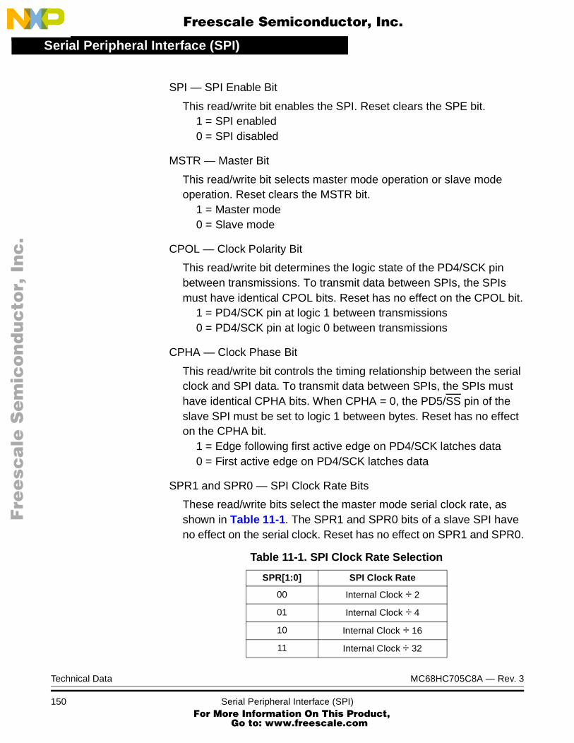
Serial Peripheral Interface (SPI)
F
ree
sca
le S
em
ico
nd
uc
tor,
I
Freescale Semiconductor, Inc.n
c..
.
SPI — SPI Enable Bit
This read/write bit enables the SPI. Reset clears the SPE bit.1 = SPI enabled0 = SPI disabled
MSTR — Master Bit
This read/write bit selects master mode operation or slave mode operation. Reset clears the MSTR bit.
1 = Master mode0 = Slave mode
CPOL — Clock Polarity Bit
This read/write bit determines the logic state of the PD4/SCK pin between transmissions. To transmit data between SPIs, the SPIs must have identical CPOL bits. Reset has no effect on the CPOL bit.
1 = PD4/SCK pin at logic 1 between transmissions0 = PD4/SCK pin at logic 0 between transmissions
CPHA — Clock Phase Bit
This read/write bit controls the timing relationship between the serial clock and SPI data. To transmit data between SPIs, the SPIs must have identical CPHA bits. When CPHA = 0, the PD5/SS pin of the slave SPI must be set to logic 1 between bytes. Reset has no effect on the CPHA bit.
1 = Edge following first active edge on PD4/SCK latches data0 = First active edge on PD4/SCK latches data
SPR1 and SPR0 — SPI Clock Rate Bits
These read/write bits select the master mode serial clock rate, as shown in Table 11-1. The SPR1 and SPR0 bits of a slave SPI have no effect on the serial clock. Reset has no effect on SPR1 and SPR0.
Table 11-1. SPI Clock Rate Selection
SPR[1:0] SPI Clock Rate
00 Internal Clock ÷ 2
01 Internal Clock ÷ 4
10 Internal Clock ÷ 16
11 Internal Clock ÷ 32
Technical Data MC68HC705C8A — Rev. 3
150 Serial Peripheral Interface (SPI) For More Information On This Product,
Go to: www.freescale.com

Serial Peripheral Interface (SPI)SPI I/O Registers
F
ree
sca
le S
em
ico
nd
uc
tor,
I
Freescale Semiconductor, Inc.n
c..
.
11.9.3 SPI Status Register
The SPSR shown in Figure 11-9 contains flags to signal these conditions:
• SPI transmission complete
• Write collision
• Mode fault
SPIF — SPI Flag
This clearable, read-only bit is set each time a byte shifts out of or into the shift register. SPIF generates an interrupt request if the SPIE bit in the SPCR is also set. Clear SPIF by reading the SPSR with SPIF set and then reading or writing the SPDR. Reset clears the SPIF bit.
1 = Transmission complete0 = Transmission not complete
WCOL — Write Collision Bit
This clearable, read-only flag is set when software writes to the SPDR while a transmission is in progress. Clear the WCOL bit by reading the SPSR with WCOL set and then reading or writing the SPDR. Reset clears WCOL.
1 = Invalid write to SPDR0 = No invalid write to SPDR
Address: $000B
Bit 7 6 5 4 3 2 1 Bit 0
Read: SPIF WCOL MODF
Write:
Reset: 0 0 0
= Unimplemented
Figure 11-9. SPI Status Register (SPSR)
MC68HC705C8A — Rev. 3 Technical Data
MOTOROLA Serial Peripheral Interface (SPI) For More Information On This Product,
Go to: www.freescale.com

Serial Peripheral Interface (SPI)
F
ree
sca
le S
em
ico
nd
uc
tor,
I
Freescale Semiconductor, Inc.n
c..
.
MODF — Mode Fault Bit
This clearable, read-only bit is set when a logic 0 occurs on the PD5/SS pin while the MSTR bit is set. MODF generates an interrupt request if the SPIE bit is also set. Clear the MODF bit by reading the SPSR with MODF set and then writing to the SPCR. Reset clears MODF.
1 = PD5/SS pulled low while MSTR bit set0 = PD5/SS not pulled low while MSTR bit set
Technical Data MC68HC705C8A — Rev. 3
152 Serial Peripheral Interface (SPI) For More Information On This Product,
Go to: www.freescale.com
F
ree
sca
le S
em
ico
nd
uc
tor,
IFreescale Semiconductor, Inc.
nc
...
Technical Data — MC68HC705C8A
Section 12. Instruction Set
12.1 Contents
12.2 Introduction . . . . . . . . . . . . . . . . . . . . . . . . . . . . . . . . . . . . . . .154
12.3 Addressing Modes . . . . . . . . . . . . . . . . . . . . . . . . . . . . . . . . .15412.3.1 Inherent . . . . . . . . . . . . . . . . . . . . . . . . . . . . . . . . . . . . . . .15512.3.2 Immediate. . . . . . . . . . . . . . . . . . . . . . . . . . . . . . . . . . . . . .15512.3.3 Direct . . . . . . . . . . . . . . . . . . . . . . . . . . . . . . . . . . . . . . . . .15512.3.4 Extended . . . . . . . . . . . . . . . . . . . . . . . . . . . . . . . . . . . . . .15512.3.5 Indexed, No Offset . . . . . . . . . . . . . . . . . . . . . . . . . . . . . . .15612.3.6 Indexed, 8-Bit Offset. . . . . . . . . . . . . . . . . . . . . . . . . . . . . .15612.3.7 Indexed, 16-Bit Offset. . . . . . . . . . . . . . . . . . . . . . . . . . . . .15612.3.8 Relative . . . . . . . . . . . . . . . . . . . . . . . . . . . . . . . . . . . . . . .157
12.4 Instruction Types . . . . . . . . . . . . . . . . . . . . . . . . . . . . . . . . . .15712.4.1 Register/Memory Instructions. . . . . . . . . . . . . . . . . . . . . . .15812.4.2 Read-Modify-Write Instructions . . . . . . . . . . . . . . . . . . . . .15912.4.3 Jump/Branch Instructions. . . . . . . . . . . . . . . . . . . . . . . . . .16012.4.4 Bit Manipulation Instructions . . . . . . . . . . . . . . . . . . . . . . .16212.4.5 Control Instructions . . . . . . . . . . . . . . . . . . . . . . . . . . . . . .163
12.5 Instruction Set Summary . . . . . . . . . . . . . . . . . . . . . . . . . . . .164
12.6 Opcode Map . . . . . . . . . . . . . . . . . . . . . . . . . . . . . . . . . . . . . .169
MC68HC705C8A — Rev. 3 Technical Data
MOTOROLA Instruction Set For More Information On This Product,
Go to: www.freescale.com
Instruction Set
F
ree
sca
le S
em
ico
nd
uc
tor,
I
Freescale Semiconductor, Inc.n
c..
.
12.2 Introduction
The MCU instruction set has 62 instructions and uses eight addressing modes. The instructions include all those of the M146805 CMOS Family plus one more: the unsigned multiply (MUL) instruction. The MUL instruction allows unsigned multiplication of the contents of the accumulator (A) and the index register (X). The high-order product is stored in the index register, and the low-order product is stored in the accumulator.
12.3 Addressing Modes
The CPU uses eight addressing modes for flexibility in accessing data. The addressing modes provide eight different ways for the CPU to find the data required to execute an instruction.
The eight addressing modes are:
• Inherent
• Immediate
• Direct
• Extended
• Indexed, no offset
• Indexed, 8-bit offset
• Indexed, 16-bit offset
• Relative
Technical Data MC68HC705C8A — Rev. 3
154 Instruction Set For More Information On This Product,
Go to: www.freescale.com

Instruction SetAddressing Modes
F
ree
sca
le S
em
ico
nd
uc
tor,
I
Freescale Semiconductor, Inc.n
c..
.
12.3.1 Inherent
Inherent instructions are those that have no operand, such as return from interrupt (RTI) and stop (STOP). Some of the inherent instructions act on data in the CPU registers, such as set carry flag (SEC) and increment accumulator (INCA). Inherent instructions require no operand address and are one byte long.
12.3.2 Immediate
Immediate instructions are those that contain a value to be used in an operation with the value in the accumulator or index register. Immediate instructions require no operand address and are two bytes long. The opcode is the first byte, and the immediate data value is the second byte.
12.3.3 Direct
Direct instructions can access any of the first 256 memory locations with two bytes. The first byte is the opcode, and the second is the low byte of the operand address. In direct addressing, the CPU automatically uses $00 as the high byte of the operand address.
12.3.4 Extended
Extended instructions use three bytes and can access any address in memory. The first byte is the opcode; the second and third bytes are the high and low bytes of the operand address.
When using the Motorola assembler, the programmer does not need to specify whether an instruction is direct or extended. The assembler automatically selects the shortest form of the instruction.
MC68HC705C8A — Rev. 3 Technical Data
MOTOROLA Instruction Set For More Information On This Product,
Go to: www.freescale.com
Instruction Set
F
ree
sca
le S
em
ico
nd
uc
tor,
I
Freescale Semiconductor, Inc.n
c..
.
12.3.5 Indexed, No Offset
Indexed instructions with no offset are 1-byte instructions that can access data with variable addresses within the first 256 memory locations. The index register contains the low byte of the effective address of the operand. The CPU automatically uses $00 as the high byte, so these instructions can address locations $0000–$00FF.
Indexed, no offset instructions are often used to move a pointer through a table or to hold the address of a frequently used RAM or I/O location.
12.3.6 Indexed, 8-Bit Offset
Indexed, 8-bit offset instructions are 2-byte instructions that can access data with variable addresses within the first 511 memory locations. The CPU adds the unsigned byte in the index register to the unsigned byte following the opcode. The sum is the effective address of the operand. These instructions can access locations $0000–$01FE.
Indexed 8-bit offset instructions are useful for selecting the kth element in an n-element table. The table can begin anywhere within the first 256 memory locations and could extend as far as location 510 ($01FE). The k value is typically in the index register, and the address of the beginning of the table is in the byte following the opcode.
12.3.7 Indexed, 16-Bit Offset
Indexed, 16-bit offset instructions are 3-byte instructions that can access data with variable addresses at any location in memory. The CPU adds the unsigned byte in the index register to the two unsigned bytes following the opcode. The sum is the effective address of the operand. The first byte after the opcode is the high byte of the 16-bit offset; the second byte is the low byte of the offset.
Indexed, 16-bit offset instructions are useful for selecting the kth element in an n-element table anywhere in memory.
As with direct and extended addressing, the Motorola assembler determines the shortest form of indexed addressing.
Technical Data MC68HC705C8A — Rev. 3
156 Instruction Set For More Information On This Product,
Go to: www.freescale.com

Instruction SetInstruction Types
F
ree
sca
le S
em
ico
nd
uc
tor,
I
Freescale Semiconductor, Inc.n
c..
.
12.3.8 Relative
Relative addressing is only for branch instructions. If the branch condition is true, the CPU finds the effective branch destination by adding the signed byte following the opcode to the contents of the program counter. If the branch condition is not true, the CPU goes to the next instruction. The offset is a signed, two’s complement byte that gives a branching range of –128 to +127 bytes from the address of the next location after the branch instruction.
When using the Motorola assembler, the programmer does not need to calculate the offset, because the assembler determines the proper offset and verifies that it is within the span of the branch.
12.4 Instruction Types
The MCU instructions fall into five categories:
• Register/memory instructions
• Read-modify-write instructions
• Jump/branch instructions
• Bit manipulation instructions
• Control instructions
MC68HC705C8A — Rev. 3 Technical Data
MOTOROLA Instruction Set For More Information On This Product,
Go to: www.freescale.com

Instruction Set
F
ree
sca
le S
em
ico
nd
uc
tor,
I
Freescale Semiconductor, Inc.n
c..
.
12.4.1 Register/Memory Instructions
These instructions operate on CPU registers and memory locations. Most of them use two operands. One operand is in either the accumulator or the index register. The CPU finds the other operand in memory.
Table 12-1. Register/Memory Instructions
Instruction Mnemonic
Add memory byte and carry bit to accumulator ADC
Add memory byte to accumulator ADD
AND memory byte with accumulator AND
Bit test accumulator BIT
Compare accumulator CMP
Compare index register with memory byte CPX
Exclusive OR accumulator with memory byte EOR
Load accumulator with memory byte LDA
Load Index register with memory byte LDX
Multiply MUL
OR accumulator with memory byte ORA
Subtract memory byte and carry bit from accumulator
SBC
Store accumulator in memory STA
Store index register in memory STX
Subtract memory byte from accumulator SUB
Technical Data MC68HC705C8A — Rev. 3
158 Instruction Set For More Information On This Product,
Go to: www.freescale.com

Instruction SetInstruction Types
F
ree
sca
le S
em
ico
nd
uc
tor,
I
Freescale Semiconductor, Inc.n
c..
.
12.4.2 Read-Modify-Write Instructions
These instructions read a memory location or a register, modify its contents, and write the modified value back to the memory location or to the register.
NOTE: Do not use read-modify-write operations on write-only registers.
Table 12-2. Read-Modify-Write Instructions
Instruction Mnemonic
Arithmetic shift left (same as LSL) ASL
Arithmetic shift right ASR
Bit clear BCLR(1)
1. Unlike other read-modify-write instructions, BCLR and BSET useonly direct addressing.
Bit set BSET(1)
Clear register CLR
Complement (one’s complement) COM
Decrement DEC
Increment INC
Logical shift left (same as ASL) LSL
Logical shift right LSR
Negate (two’s complement) NEG
Rotate left through carry bit ROL
Rotate right through carry bit ROR
Test for negative or zero TST(2)
2. TST is an exception to the read-modify-write sequence because itdoes not write a replacement value.
MC68HC705C8A — Rev. 3 Technical Data
MOTOROLA Instruction Set For More Information On This Product,
Go to: www.freescale.com

Instruction Set
F
ree
sca
le S
em
ico
nd
uc
tor,
I
Freescale Semiconductor, Inc.n
c..
.
12.4.3 Jump/Branch Instructions
Jump instructions allow the CPU to interrupt the normal sequence of the program counter. The unconditional jump instruction (JMP) and the jump-to-subroutine instruction (JSR) have no register operand. Branch instructions allow the CPU to interrupt the normal sequence of the program counter when a test condition is met. If the test condition is not met, the branch is not performed.
The BRCLR and BRSET instructions cause a branch based on the state of any readable bit in the first 256 memory locations. These 3-byte instructions use a combination of direct addressing and relative addressing. The direct address of the byte to be tested is in the byte following the opcode. The third byte is the signed offset byte. The CPU finds the effective branch destination by adding the third byte to the program counter if the specified bit tests true. The bit to be tested and its condition (set or clear) is part of the opcode. The span of branching is from –128 to +127 from the address of the next location after the branch instruction. The CPU also transfers the tested bit to the carry/borrow bit of the condition code register.
Technical Data MC68HC705C8A — Rev. 3
160 Instruction Set For More Information On This Product,
Go to: www.freescale.com

Instruction SetInstruction Types
F
ree
sca
le S
em
ico
nd
uc
tor,
I
Freescale Semiconductor, Inc.n
c..
.
Table 12-3. Jump and Branch Instructions
Instruction Mnemonic
Branch if carry bit clear BCC
Branch if carry bit set BCS
Branch if equal BEQ
Branch if half-carry bit clear BHCC
Branch if half-carry bit set BHCS
Branch if higher BHI
Branch if higher or same BHS
Branch if IRQ pin high BIH
Branch if IRQ pin low BIL
Branch if lower BLO
Branch if lower or same BLS
Branch if interrupt mask clear BMC
Branch if minus BMI
Branch if interrupt mask set BMS
Branch if not equal BNE
Branch if plus BPL
Branch always BRA
Branch if bit clear BRCLR
Branch never BRN
Branch if bit set BRSET
Branch to subroutine BSR
Unconditional jump JMP
Jump to subroutine JSR
MC68HC705C8A — Rev. 3 Technical Data
MOTOROLA Instruction Set For More Information On This Product,
Go to: www.freescale.com

Instruction Set
F
ree
sca
le S
em
ico
nd
uc
tor,
I
Freescale Semiconductor, Inc.n
c..
.
12.4.4 Bit Manipulation Instructions
The CPU can set or clear any writable bit in the first 256 bytes of memory, which includes I/O registers and on-chip RAM locations. The CPU can also test and branch based on the state of any bit in any of the first 256 memory locations.
Table 12-4. Bit Manipulation Instructions
Instruction Mnemonic
Bit clear BCLR
Branch if bit clear BRCLR
Branch if bit set BRSET
Bit set BSET
Technical Data MC68HC705C8A — Rev. 3
162 Instruction Set For More Information On This Product,
Go to: www.freescale.com

Instruction SetInstruction Types
F
ree
sca
le S
em
ico
nd
uc
tor,
I
Freescale Semiconductor, Inc.n
c..
.
12.4.5 Control Instructions
These instructions act on CPU registers and control CPU operation during program execution.
Table 12-5. Control Instructions
Instruction Mnemonic
Clear carry bit CLC
Clear interrupt mask CLI
No operation NOP
Reset stack pointer RSP
Return from interrupt RTI
Return from subroutine RTS
Set carry bit SEC
Set interrupt mask SEI
Stop oscillator and enable IRQ pin STOP
Software interrupt SWI
Transfer accumulator to index register TAX
Transfer index register to accumulator TXA
Stop CPU clock and enable interrupts WAIT
MC68HC705C8A — Rev. 3 Technical Data
MOTOROLA Instruction Set For More Information On This Product,
Go to: www.freescale.com

Instruction Set
F
ree
sca
le S
em
ico
nd
uc
tor,
I
Freescale Semiconductor, Inc.n
c..
.
12.5 Instruction Set Summary
Table 12-6. Instruction Set Summary (Sheet 1 of 6)
SourceForm Operation Description
Effect onCCR
Ad
dre
ssM
od
e
Op
cod
e
Op
eran
d
Cyc
les
H I N Z C
ADC #oprADC oprADC oprADC opr,XADC opr,XADC ,X
Add with Carry A ← (A) + (M) + (C) —
IMMDIREXTIX2IX1IX
A9B9C9D9E9F9
iidd
hh llee ff
ff
234543
ADD #oprADD oprADD oprADD opr,XADD opr,XADD ,X
Add without Carry A ← (A) + (M) —
IMMDIREXTIX2IX1IX
ABBBCBDBEBFB
iidd
hh llee ff
ff
234543
AND #oprAND oprAND oprAND opr,XAND opr,XAND ,X
Logical AND A ← (A) ∧ (M) — — —
IMMDIREXTIX2IX1IX
A4B4C4D4E4F4
iidd
hh llee ff
ff
234543
ASL oprASLAASLXASL opr,XASL ,X
Arithmetic Shift Left (Same as LSL) — —
DIRINHINHIX1IX
3848586878
dd
ff
53365
ASR oprASRAASRXASR opr,XASR ,X
Arithmetic Shift Right — —
DIRINHINHIX1IX
3747576777
dd
ff
53365
BCC rel Branch if Carry Bit Clear PC ← (PC) + 2 + rel ? C = 0 — — — — — REL 24 rr 3
BCLR n opr Clear Bit n Mn ← 0 — — — — —
DIR (b0)DIR (b1)DIR (b2)DIR (b3)DIR (b4)DIR (b5)DIR (b6)DIR (b7)
11131517191B1D1F
dddddddddddddddd
55555555
BCS rel Branch if Carry Bit Set (Same as BLO) PC ← (PC) + 2 + rel ? C = 1 — — — — — REL 25 rr 3
BEQ rel Branch if Equal PC ← (PC) + 2 + rel ? Z = 1 — — — — — REL 27 rr 3
BHCC rel Branch if Half-Carry Bit Clear PC ← (PC) + 2 + rel ? H = 0 — — — — — REL 28 rr 3
BHCS rel Branch if Half-Carry Bit Set PC ← (PC) + 2 + rel ? H = 1 — — — — — REL 29 rr 3
BHI rel Branch if Higher PC ← (PC) + 2 + rel ? C ∨ Z = 0 — — — — — REL 22 rr 3
BHS rel Branch if Higher or Same PC ← (PC) + 2 + rel ? C = 0 — — — — — REL 24 rr 3
C
b0b7
0
b0b7
C
Technical Data MC68HC705C8A — Rev. 3
164 Instruction Set For More Information On This Product,
Go to: www.freescale.com

Instruction SetInstruction Set Summary
F
ree
sca
le S
em
ico
nd
uc
tor,
I
Freescale Semiconductor, Inc.n
c..
.
BIH rel Branch if IRQ Pin High PC ← (PC) + 2 + rel ? IRQ = 1 — — — — — REL 2F rr 3
BIL rel Branch if IRQ Pin Low PC ← (PC) + 2 + rel ? IRQ = 0 — — — — — REL 2E rr 3
BIT #oprBIT oprBIT oprBIT opr,XBIT opr,XBIT ,X
Bit Test Accumulator with Memory Byte (A) ∧ (M) — — —
IMMDIREXTIX2IX1IX
A5B5C5D5E5F5
iidd
hh llee ff
ff
234543
BLO rel Branch if Lower (Same as BCS) PC ← (PC) + 2 + rel ? C = 1 — — — — — REL 25 rr 3
BLS rel Branch if Lower or Same PC ← (PC) + 2 + rel ? C ∨ Z = 1 — — — — — REL 23 rr 3
BMC rel Branch if Interrupt Mask Clear PC ← (PC) + 2 + rel ? I = 0 — — — — — REL 2C rr 3
BMI rel Branch if Minus PC ← (PC) + 2 + rel ? N = 1 — — — — — REL 2B rr 3
BMS rel Branch if Interrupt Mask Set PC ← (PC) + 2 + rel ? I = 1 — — — — — REL 2D rr 3
BNE rel Branch if Not Equal PC ← (PC) + 2 + rel ? Z = 0 — — — — — REL 26 rr 3
BPL rel Branch if Plus PC ← (PC) + 2 + rel ? N = 0 — — — — — REL 2A rr 3
BRA rel Branch Always PC ← (PC) + 2 + rel ? 1 = 1 — — — — — REL 20 rr 3
BRCLR n opr rel Branch if Bit n Clear PC ← (PC) + 2 + rel ? Mn = 0 — — — —
DIR (b0)DIR (b1)DIR (b2)DIR (b3)DIR (b4)DIR (b5)DIR (b6)DIR (b7)
01030507090B0D0F
dd rrdd rrdd rrdd rrdd rrdd rrdd rrdd rr
55555555
BRN rel Branch Never PC ← (PC) + 2 + rel ? 1 = 0 — — — — — REL 21 rr 3
BRSET n opr rel Branch if Bit n Set PC ← (PC) + 2 + rel ? Mn = 1 — — — —
DIR (b0)DIR (b1)DIR (b2)DIR (b3)DIR (b4)DIR (b5)DIR (b6)DIR (b7)
00020406080A0C0E
dd rrdd rrdd rrdd rrdd rrdd rrdd rrdd rr
55555555
BSET n opr Set Bit n Mn ← 1 — — — — —
DIR (b0)DIR (b1)DIR (b2)DIR (b3)DIR (b4)DIR (b5)DIR (b6)DIR (b7)
10121416181A1C1E
dddddddddddddddd
55555555
BSR rel Branch to Subroutine
PC ← (PC) + 2; push (PCL)SP ← (SP) – 1; push (PCH)
SP ← (SP) – 1PC ← (PC) + rel
— — — — — REL AD rr 6
CLC Clear Carry Bit C ← 0 — — — — 0 INH 98 2
CLI Clear Interrupt Mask I ← 0 — 0 — — — INH 9A 2
Table 12-6. Instruction Set Summary (Sheet 2 of 6)
SourceForm Operation Description
Effect onCCR
Ad
dre
ssM
od
e
Op
cod
e
Op
eran
d
Cyc
les
H I N Z C
MC68HC705C8A — Rev. 3 Technical Data
MOTOROLA Instruction Set For More Information On This Product,
Go to: www.freescale.com

Instruction Set
F
ree
sca
le S
em
ico
nd
uc
tor,
I
Freescale Semiconductor, Inc.n
c..
.
CLR oprCLRACLRXCLR opr,XCLR ,X
Clear Byte
M ← $00A ← $00X ← $00M ← $00M ← $00
— — 0 1 —
DIRINHINHIX1IX
3F4F5F6F7F
dd
ff
53365
CMP #oprCMP oprCMP oprCMP opr,XCMP opr,XCMP ,X
Compare Accumulator with Memory Byte (A) – (M) — —
IMMDIREXTIX2IX1IX
A1B1C1D1E1F1
iidd
hh llee ff
ff
234543
COM oprCOMACOMXCOM opr,XCOM ,X
Complement Byte (One’s Complement)
M ← (M) = $FF – (M)A ← (A) = $FF – (A)X ← (X) = $FF – (X)M ← (M) = $FF – (M)M ← (M) = $FF – (M)
— — 1
DIRINHINHIX1IX
3343536373
dd
ff
53365
CPX #oprCPX oprCPX oprCPX opr,XCPX opr,XCPX ,X
Compare Index Register with Memory Byte (X) – (M) — —
IMMDIREXTIX2IX1IX
A3B3C3D3E3F3
iidd
hh llee ff
ff
234543
DEC oprDECADECXDEC opr,XDEC ,X
Decrement Byte
M ← (M) – 1A ← (A) – 1X ← (X) – 1M ← (M) – 1M ← (M) – 1
— — —
DIRINHINHIX1IX
3A4A5A6A7A
dd
ff
53365
EOR #oprEOR oprEOR oprEOR opr,XEOR opr,XEOR ,X
EXCLUSIVE OR Accumulator with Memory Byte
A ← (A) ⊕ (M) — — —
IMMDIREXTIX2IX1IX
A8B8C8D8E8F8
iidd
hh llee ff
ff
234543
INC oprINCAINCXINC opr,XINC ,X
Increment Byte
M ← (M) + 1A ← (A) + 1X ← (X) + 1M ← (M) + 1M ← (M) + 1
— — —
DIRINHINHIX1IX
3C4C5C6C7C
dd
ff
53365
JMP oprJMP oprJMP opr,XJMP opr,XJMP ,X
Unconditional Jump PC ← Jump Address — — — — —
DIREXTIX2IX1IX
BCCCDCECFC
ddhh llee ff
ff
23432
Table 12-6. Instruction Set Summary (Sheet 3 of 6)
SourceForm Operation Description
Effect onCCR
Ad
dre
ssM
od
e
Op
cod
e
Op
eran
d
Cyc
les
H I N Z C
Technical Data MC68HC705C8A — Rev. 3
166 Instruction Set For More Information On This Product,
Go to: www.freescale.com
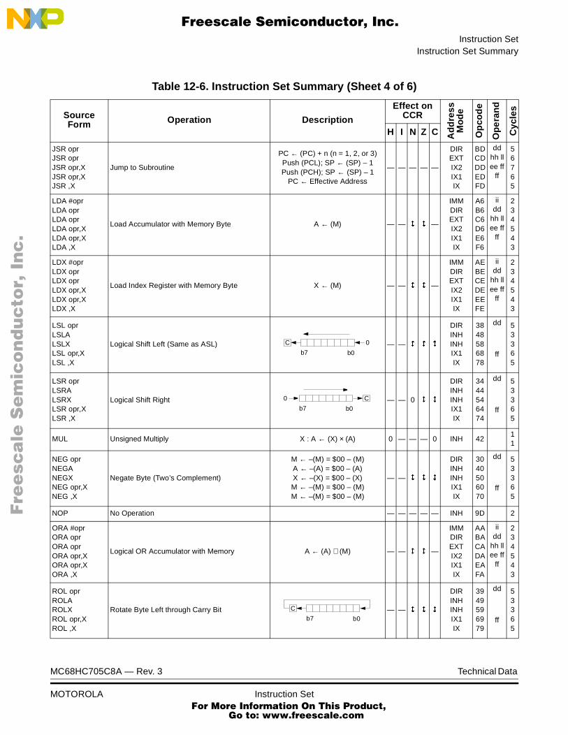
Instruction SetInstruction Set Summary
F
ree
sca
le S
em
ico
nd
uc
tor,
I
Freescale Semiconductor, Inc.n
c..
.
JSR oprJSR oprJSR opr,XJSR opr,XJSR ,X
Jump to Subroutine
PC ← (PC) + n (n = 1, 2, or 3)Push (PCL); SP ← (SP) – 1Push (PCH); SP ← (SP) – 1
PC ← Effective Address
— — — — —
DIREXTIX2IX1IX
BDCDDDEDFD
ddhh llee ff
ff
56765
LDA #oprLDA oprLDA oprLDA opr,XLDA opr,XLDA ,X
Load Accumulator with Memory Byte A ← (M) — — —
IMMDIREXTIX2IX1IX
A6B6C6D6E6F6
iidd
hh llee ff
ff
234543
LDX #oprLDX oprLDX oprLDX opr,XLDX opr,XLDX ,X
Load Index Register with Memory Byte X ← (M) — — —
IMMDIREXTIX2IX1IX
AEBECEDEEEFE
iidd
hh llee ff
ff
234543
LSL oprLSLALSLXLSL opr,XLSL ,X
Logical Shift Left (Same as ASL) — —
DIRINHINHIX1IX
3848586878
dd
ff
53365
LSR oprLSRALSRXLSR opr,XLSR ,X
Logical Shift Right — — 0
DIRINHINHIX1IX
3444546474
dd
ff
53365
MUL Unsigned Multiply X : A ← (X) × (A) 0 — — — 0 INH 4211
NEG oprNEGANEGXNEG opr,XNEG ,X
Negate Byte (Two’s Complement)
M ← –(M) = $00 – (M)A ← –(A) = $00 – (A)X ← –(X) = $00 – (X)M ← –(M) = $00 – (M)M ← –(M) = $00 – (M)
— —
DIRINHINHIX1IX
3040506070
dd
ff
53365
NOP No Operation — — — — — INH 9D 2
ORA #oprORA oprORA oprORA opr,XORA opr,XORA ,X
Logical OR Accumulator with Memory A ← (A) ∨ (M) — — —
IMMDIREXTIX2IX1IX
AABACADAEAFA
iidd
hh llee ff
ff
234543
ROL oprROLAROLXROL opr,XROL ,X
Rotate Byte Left through Carry Bit — —
DIRINHINHIX1IX
3949596979
dd
ff
53365
Table 12-6. Instruction Set Summary (Sheet 4 of 6)
SourceForm Operation Description
Effect onCCR
Ad
dre
ssM
od
e
Op
cod
e
Op
eran
d
Cyc
les
H I N Z C
C
b0b7
0
b0b7
C0
C
b0b7
MC68HC705C8A — Rev. 3 Technical Data
MOTOROLA Instruction Set For More Information On This Product,
Go to: www.freescale.com

Instruction Set
F
ree
sca
le S
em
ico
nd
uc
tor,
I
Freescale Semiconductor, Inc.n
c..
.
ROR oprRORARORXROR opr,XROR ,X
Rotate Byte Right through Carry Bit — —
DIRINHINHIX1IX
3646566676
dd
ff
53365
RSP Reset Stack Pointer SP ← $00FF — — — — — INH 9C 2
RTI Return from Interrupt
SP ← (SP) + 1; Pull (CCR)SP ← (SP) + 1; Pull (A)SP ← (SP) + 1; Pull (X)
SP ← (SP) + 1; Pull (PCH)SP ← (SP) + 1; Pull (PCL)
INH 80 9
RTS Return from SubroutineSP ← (SP) + 1; Pull (PCH)SP ← (SP) + 1; Pull (PCL)
— — — — — INH 81 6
SBC #oprSBC oprSBC oprSBC opr,XSBC opr,XSBC ,X
Subtract Memory Byte and Carry Bit from Accumulator
A ← (A) – (M) – (C) — —
IMMDIREXTIX2IX1IX
A2B2C2D2E2F2
iidd
hh llee ff
ff
234543
SEC Set Carry Bit C ← 1 — — — — 1 INH 99 2
SEI Set Interrupt Mask I ← 1 — 1 — — — INH 9B 2
STA oprSTA oprSTA opr,XSTA opr,XSTA ,X
Store Accumulator in Memory M ← (A) — — —
DIREXTIX2IX1IX
B7C7D7E7F7
ddhh llee ff
ff
45654
STOP Stop Oscillator and Enable IRQ Pin — 0 — — — INH 8E 2
STX oprSTX oprSTX opr,XSTX opr,XSTX ,X
Store Index Register In Memory M ← (X) — — —
DIREXTIX2IX1IX
BFCFDFEFFF
ddhh llee ff
ff
45654
SUB #oprSUB oprSUB oprSUB opr,XSUB opr,XSUB ,X
Subtract Memory Byte from Accumulator A ← (A) – (M) — —
IMMDIREXTIX2IX1IX
A0B0C0D0E0F0
iidd
hh llee ff
ff
234543
SWI Software Interrupt
PC ← (PC) + 1; Push (PCL)SP ← (SP) – 1; Push (PCH)
SP ← (SP) – 1; Push (X)SP ← (SP) – 1; Push (A)
SP ← (SP) – 1; Push (CCR)SP ← (SP) – 1; I ← 1
PCH ← Interrupt Vector High BytePCL ← Interrupt Vector Low Byte
— 1 — — — INH 8310
TAX Transfer Accumulator to Index Register X ← (A) — — — — — INH 97 2
Table 12-6. Instruction Set Summary (Sheet 5 of 6)
SourceForm Operation Description
Effect onCCR
Ad
dre
ssM
od
e
Op
cod
e
Op
eran
d
Cyc
les
H I N Z C
b0b7
C
Technical Data MC68HC705C8A — Rev. 3
168 Instruction Set For More Information On This Product,
Go to: www.freescale.com

Instruction SetOpcode Map
F
ree
sca
le S
em
ico
nd
uc
tor,
I
Freescale Semiconductor, Inc.n
c..
.
12.6 Opcode Map
See Table 12-7.
TST oprTSTATSTXTST opr,XTST ,X
Test Memory Byte for Negative or Zero (M) – $00 — — —
DIRINHINHIX1IX
3D4D5D6D7D
dd
ff
43354
TXA Transfer Index Register to Accumulator A ← (X) — — — — — INH 9F 2
WAIT Stop CPU Clock and Enable Interrupts — — — — INH 8F 2
A Accumulator opr Operand (one or two bytes)C Carry/borrow flag PC Program counterCCR Condition code register PCH Program counter high bytedd Direct address of operand PCL Program counter low bytedd rr Direct address of operand and relative offset of branch instruction REL Relative addressing modeDIR Direct addressing mode rel Relative program counter offset byteee ff High and low bytes of offset in indexed, 16-bit offset addressing rr Relative program counter offset byteEXT Extended addressing mode SP Stack pointerff Offset byte in indexed, 8-bit offset addressing X Index registerH Half-carry flag Z Zero flaghh ll High and low bytes of operand address in extended addressing # Immediate valueI Interrupt mask ∧ Logical ANDii Immediate operand byte ∨ Logical ORIMM Immediate addressing mode ⊕ Logical EXCLUSIVE ORINH Inherent addressing mode ( ) Contents ofIX Indexed, no offset addressing mode –( ) Negation (two’s complement)IX1 Indexed, 8-bit offset addressing mode ← Loaded withIX2 Indexed, 16-bit offset addressing mode ? IfM Memory location : Concatenated withN Negative flag Set or clearedn Any bit — Not affected
Table 12-6. Instruction Set Summary (Sheet 6 of 6)
SourceForm Operation Description
Effect onCCR
Ad
dre
ssM
od
e
Op
cod
e
Op
eran
d
Cyc
les
H I N Z C
MC68HC705C8A — Rev. 3 Technical Data
MOTOROLA Instruction Set For More Information On This Product,
Go to: www.freescale.com

Instruction Set
SB
F
ree
sca
le S
em
ico
nd
uc
tor,
I
Freescale Semiconductor, Inc.n
c..
.
Tab
le 1
2-7.
Op
cod
e M
ap
Bit
Man
ipu
lati
on
Bra
nch
Rea
d-M
od
ify-
Wri
teC
on
tro
lR
egis
ter/
Mem
ory
DIR
DIR
RE
LD
IRIN
HIN
HIX
1IX
INH
INH
IMM
DIR
EX
TIX
2IX
1IX
01
23
45
67
89
AB
CD
EF
05
BR
SE
T0
3D
I R
5B
SE
T0
2D
I R
3B
RA
2R
EL
5N
EG
2D
I R
3N
EG
A1
I NH
3N
EG
X1
I NH
6N
EG
2IX
1
5N
EG
1IX
9R
TI
1I N
H
2S
UB
2I M
M
3S
UB
2D
I R
4S
UB
3E
XT
5S
UB
3IX
2
4S
UB
2IX
1
3S
UB
1I X
0
15
BR
CL
R0
3D
I R
5B
CLR
02
DI R
3B
RN
2R
EL
6R
TS
1I N
H
2C
MP
2I M
M
3C
MP
2D
I R
4C
MP
3E
XT
5C
MP
3IX
2
4C
MP
2IX
1
3C
MP
1I X
1
25
BR
SE
T1
3D
I R
5B
SE
T1
2D
I R
3B
HI
2R
EL
11M
UL
1I N
H
2S
BC
2I M
M
3S
BC
2D
I R
4S
BC
3E
XT
5S
BC
3IX
2
4S
BC
2IX
1
3S
BC
1I X
2
35
BR
CL
R1
3D
I R
5B
CLR
12
DI R
3B
LS2
RE
L
5C
OM
2D
I R
3C
OM
A1
I NH
3C
OM
X1
I NH
6C
OM
2IX
1
5C
OM
1IX
10S
WI
1I N
H
2C
PX
2I M
M
3C
PX
2D
I R
4C
PX
3E
XT
5C
PX
3IX
2
4C
PX
2IX
1
3C
PX
1I X
3
45
BR
SE
T2
3D
I R
5B
SE
T2
2D
I R
3B
CC
2R
EL
5LS
R2
DI R
3LS
RA
1I N
H
3LS
RX
1I N
H
6LS
R2
IX1
5LS
R1
IX
2A
ND
2I M
M
3A
ND
2D
I R
4A
ND
3E
XT
5A
ND
3IX
2
4A
ND
2IX
1
3A
ND
1I X
4
55
BR
CL
R2
3D
IR
5B
CLR
22
DIR
3B
CS
/BLO
2R
EL
2B
IT2
IMM
3B
IT2
DIR
4B
IT3
EX
T
5B
IT3
IX2
4B
IT2
IX1
3B
IT1
IX5
65
BR
SE
T3
3D
IR
5B
SE
T3
2D
IR
3B
NE
2R
EL
5R
OR
2D
IR
3R
OR
A1
INH
3R
OR
X1
INH
6R
OR
2IX
1
5R
OR
1IX
2LD
A2
IMM
3LD
A2
DIR
4LD
A3
EX
T
5LD
A3
IX2
4LD
A2
IX1
3LD
A1
IX6
75
BR
CL
R3
3D
IR
5B
CLR
32
DIR
3B
EQ
2R
EL
5A
SR
2D
IR
3A
SR
A1
INH
3A
SR
X1
INH
6A
SR
2IX
1
5A
SR
1IX
2TA
X1
INH
4S
TA2
DIR
5S
TA3
EX
T
6S
TA3
IX2
5S
TA2
IX1
4S
TA1
IX7
85
BR
SE
T4
3D
IR
5B
SE
T4
2D
IR
3B
HC
C2
RE
L
5A
SL/
LSL
2D
IR
3A
SLA
/LS
LA1
INH
3A
SLX
/LS
LX1
INH
6A
SL/
LSL
2IX
1
5A
SL/
LSL
1IX
2C
LC
1IN
H
2E
OR
2IM
M
3E
OR
2D
IR
4E
OR
3E
XT
5E
OR
3IX
2
4E
OR
2IX
1
3E
OR
1IX
8
95
BR
CL
R4
3D
IR
5B
CLR
42
DIR
3B
HC
S2
RE
L
5R
OL
2D
IR
3R
OLA
1IN
H
3R
OLX
1IN
H
6R
OL
2IX
1
5R
OL
1IX
2S
EC
1IN
H
2A
DC
2IM
M
3A
DC
2D
IR
4A
DC
3E
XT
5A
DC
3IX
2
4A
DC
2IX
1
3A
DC
1IX
9
A5
BR
SE
T5
3D
IR
5B
SE
T5
2D
IR
3B
PL
2R
EL
5D
EC
2D
IR
3D
EC
A1
INH
3D
EC
X1
INH
6D
EC
2IX
1
5D
EC
1IX
2C
LI1
INH
2O
RA
2IM
M
3O
RA
2D
IR
4O
RA
3E
XT
5O
RA
3IX
2
4O
RA
2IX
1
3O
RA
1IX
A
B5
BR
CL
R5
3D
IR
5B
CLR
52
DIR
3B
MI
2R
EL
2S
EI
1IN
H
2A
DD
2IM
M
3A
DD
2D
IR
4A
DD
3E
XT
5A
DD
3IX
2
4A
DD
2IX
1
3A
DD
1IX
B
C5
BR
SE
T6
3D
IR
5B
SE
T6
2D
IR
3B
MC
2R
EL
5IN
C2
DIR
3IN
CA
1IN
H
3IN
CX
1IN
H
6IN
C2
IX1
5IN
C1
IX
2R
SP
1IN
H
2JM
P2
DIR
3JM
P3
EX
T
4JM
P3
IX2
3JM
P2
IX1
2JM
P1
IXC
D5
BR
CL
R6
3D
IR
5B
CLR
62
DIR
3B
MS
2R
EL
4T
ST
2D
IR
3T
STA
1IN
H
3T
ST
X1
INH
5T
ST
2IX
1
4T
ST
1IX
2N
OP
1IN
H
6B
SR
2R
EL
5JS
R2
DIR
6JS
R3
EX
T
7JS
R3
IX2
6JS
R2
IX1
5JS
R1
IXD
E5
BR
SE
T7
3D
IR
5B
SE
T7
2D
IR
3B
IL2
RE
L
2S
TO
P1
INH
2LD
X2
IMM
3LD
X2
DIR
4LD
X3
EX
T
5LD
X3
IX2
4LD
X2
IX1
3LD
X1
IXE
F5
BR
CL
R7
3D
IR
5B
CLR
72
DIR
3B
IH2
RE
L
5C
LR
2D
IR
3C
LR
A1
INH
3C
LRX
1IN
H
6C
LR
2IX
1
5C
LR1
IX
2W
AIT
1IN
H
2T
XA
1IN
H
4S
TX
2D
IR
5S
TX
3E
XT
6S
TX
3IX
2
5S
TX
2IX
1
4S
TX
1IX
F
INH
= In
here
ntR
EL
= R
elat
ive
IMM
= Im
med
iate
IX =
Inde
xed,
No
Offs
etD
IR =
Dire
ctIX
1 =
Inde
xed,
8-B
it O
ffset
EX
T =
Ext
ende
dIX
2 =
Inde
xed,
16-
Bit
Offs
et
0M
SB
of O
pcod
e in
Hex
adec
imal
LSB
of O
pcod
e in
Hex
adec
imal
05
BR
SE
T0
3D
IR
Num
ber
of C
ycle
sO
pcod
e M
nem
onic
Num
ber
of B
ytes
/Add
ress
ing
Mod
e
SBM
SB
LM
SB
LSB
MS
B
Technical Data MC68HC705C8A — Rev. 3
170 Instruction Set
L
For More Information On This Product,
Go to: www.freescale.com

F
ree
sca
le S
em
ico
nd
uc
tor,
IFreescale Semiconductor, Inc.
nc
...
Technical Data — MC68HC705C8A
Section 13. Electrical Specifications
13.1 Contents
13.2 Introduction . . . . . . . . . . . . . . . . . . . . . . . . . . . . . . . . . . . . . . .171
13.3 Maximum Ratings . . . . . . . . . . . . . . . . . . . . . . . . . . . . . . . . . .172
13.4 Operating Temperature Range. . . . . . . . . . . . . . . . . . . . . . . .173
13.5 Thermal Characteristics . . . . . . . . . . . . . . . . . . . . . . . . . . . . .173
13.6 Power Considerations. . . . . . . . . . . . . . . . . . . . . . . . . . . . . . .174
13.7 5.0-Volt DC Electrical Characteristics. . . . . . . . . . . . . . . . . . .175
13.8 3.3-Volt DC Electrical Characteristics . . . . . . . . . . . . . . . . . .176
13.9 5.0-Volt Control Timing . . . . . . . . . . . . . . . . . . . . . . . . . . . . . .181
13.10 3.3-Volt Control Timing . . . . . . . . . . . . . . . . . . . . . . . . . . . . . .182
13.11 5.0-Volt Serial Peripheral Interface (SPI) Timing . . . . . . . . . .185
13.12 3.3-Volt Serial Peripheral Interface (SPI) Timing . . . . . . . . . .187
13.2 Introduction
This section contains electrical and timing specifications.
MC68HC705C8A — Rev. 3 Technical Data
MOTOROLA Electrical Specifications For More Information On This Product,
Go to: www.freescale.com
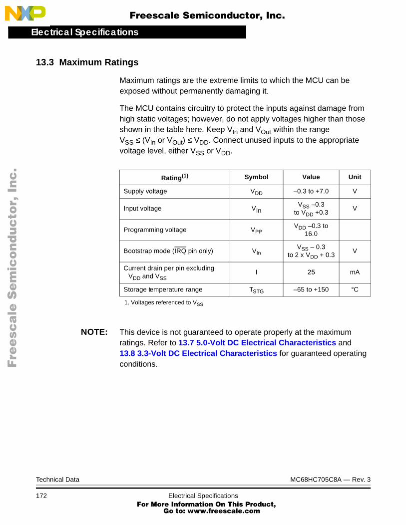
Electrical Specifications
F
ree
sca
le S
em
ico
nd
uc
tor,
I
Freescale Semiconductor, Inc.n
c..
.
13.3 Maximum Ratings
Maximum ratings are the extreme limits to which the MCU can be exposed without permanently damaging it.
The MCU contains circuitry to protect the inputs against damage from high static voltages; however, do not apply voltages higher than those shown in the table here. Keep VIn and VOut within the range VSS ≤ (VIn or VOut) ≤ VDD. Connect unused inputs to the appropriate voltage level, either VSS or VDD.
NOTE: This device is not guaranteed to operate properly at the maximum ratings. Refer to 13.7 5.0-Volt DC Electrical Characteristics and13.8 3.3-Volt DC Electrical Characteristics for guaranteed operating conditions.
Rating(1)
1. Voltages referenced to VSS
Symbol Value Unit
Supply voltage VDD –0.3 to +7.0 V
Input voltage VInVSS –0.3
to VDD +0.3V
Programming voltage VPPVDD –0.3 to
16.0
Bootstrap mode (IRQ pin only) VInVSS – 0.3
to 2 x VDD + 0.3V
Current drain per pin excluding VDD and VSS
I 25 mA
Storage temperature range TSTG –65 to +150 °C
Technical Data MC68HC705C8A — Rev. 3
172 Electrical Specifications For More Information On This Product,
Go to: www.freescale.com
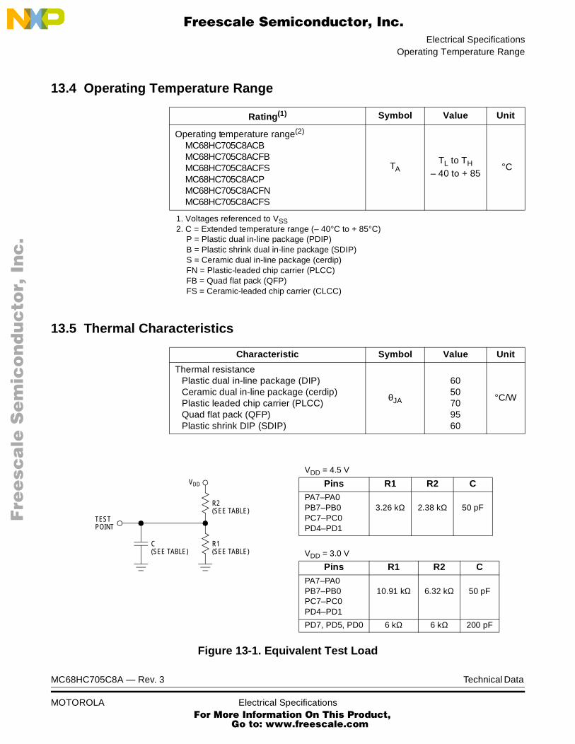
Electrical SpecificationsOperating Temperature Range
F
ree
sca
le S
em
ico
nd
uc
tor,
I
Freescale Semiconductor, Inc.n
c..
.
13.4 Operating Temperature Range
13.5 Thermal Characteristics
Figure 13-1. Equivalent Test Load
Rating(1)
1. Voltages referenced to VSS
Symbol Value Unit
Operating temperature range(2) MC68HC705C8ACBMC68HC705C8ACFBMC68HC705C8ACFSMC68HC705C8ACPMC68HC705C8ACFNMC68HC705C8ACFS
2. C = Extended temperature range (– 40°C to + 85°C)P = Plastic dual in-line package (PDIP)B = Plastic shrink dual in-line package (SDIP)S = Ceramic dual in-line package (cerdip)FN = Plastic-leaded chip carrier (PLCC)FB = Quad flat pack (QFP)FS = Ceramic-leaded chip carrier (CLCC)
TATL to TH
– 40 to + 85 °C
Characteristic Symbol Value Unit
Thermal resistancePlastic dual in-line package (DIP)Ceramic dual in-line package (cerdip)Plastic leaded chip carrier (PLCC)Quad flat pack (QFP)Plastic shrink DIP (SDIP)
θJA
6050709560
°C/W
VDD
C
R2
R1
TESTPOINT
(SEE TABLE) (SEE TABLE)
(SEE TABLE)
VDD = 4.5 V
Pins R1 R2 CPA7–PA0PB7–PB0PC7–PC0PD4–PD1
3.26 kΩ 2.38 kΩ 50 pF
VDD = 3.0 V
Pins R1 R2 CPA7–PA0PB7–PB0PC7–PC0PD4–PD1
10.91 kΩ 6.32 kΩ 50 pF
PD7, PD5, PD0 6 kΩ 6 kΩ 200 pF
MC68HC705C8A — Rev. 3 Technical Data
MOTOROLA Electrical Specifications For More Information On This Product,
Go to: www.freescale.com

Electrical Specifications
F
ree
sca
le S
em
ico
nd
uc
tor,
I
Freescale Semiconductor, Inc.n
c..
.
13.6 Power Considerations
The average chip junction temperature, TJ, in °C can be obtained from:
TJ = TA + (PD x θJA) (1)
Where:TA = ambient temperature in °CθJA = package thermal resistance, junction to ambient in °C/WPD = PINT + PI/OPINT = ICC × VCC = chip internal power dissipationPI/O = power dissipation on input and output pins (user-determined)
For most applications, PI/O < PINT and can be neglected.
Ignoring PI/O, the relationship between PD and TJ is approximately:
(2)
Solving equations (1) and (2) for K gives:
= PD x (TA + 273°C) + θJA x (PD)2 (3)
where K is a constant pertaining to the particular part. K can be determined from equation (3) by measuring PD (at equilibrium) for a known TA. Using this value of K, the values of PD and TJ can be obtained by solving equations (1) and (2) iteratively for any value of TA.
PD = TJ + 273°C
K
Technical Data MC68HC705C8A — Rev. 3
174 Electrical Specifications For More Information On This Product,
Go to: www.freescale.com
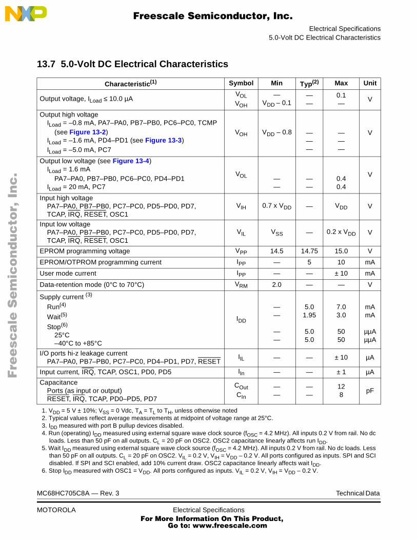
Electrical Specifications5.0-Volt DC Electrical Characteristics
F
ree
sca
le S
em
ico
nd
uc
tor,
I
Freescale Semiconductor, Inc.n
c..
.
13.7 5.0-Volt DC Electrical Characteristics
Characteristic(1)
1. VDD = 5 V ± 10%; VSS = 0 Vdc, TA = TL to TH, unless otherwise noted
Symbol Min Typ(2)
2. Typical values reflect average measurements at midpoint of voltage range at 25°C.
Max Unit
Output voltage, ILoad ≤ 10.0 µAVOL
VOH
—VDD – 0.1
——
0.1—
V
Output high voltageILoad = –0.8 mA, PA7–PA0, PB7–PB0, PC6–PC0, TCMP
(see Figure 13-2)ILoad = –1.6 mA, PD4–PD1 (see Figure 13-3)ILoad = –5.0 mA, PC7
VOH VDD – 0.8 ———
———
V
Output low voltage (see Figure 13-4)ILoad = 1.6 mA
PA7–PA0, PB7–PB0, PC6–PC0, PD4–PD1ILoad = 20 mA, PC7
VOL ——
——
0.40.4
V
Input high voltagePA7–PA0, PB7–PB0, PC7–PC0, PD5–PD0, PD7, TCAP, IRQ, RESET, OSC1
VIH 0.7 x VDD — VDD V
Input low voltagePA7–PA0, PB7–PB0, PC7–PC0, PD5–PD0, PD7, TCAP, IRQ, RESET, OSC1
VIL VSS — 0.2 x VDD V
EPROM programming voltage VPP 14.5 14.75 15.0 V
EPROM/OTPROM programming current IPP — 5 10 mA
User mode current IPP — — ± 10 mA
Data-retention mode (0°C to 70°C) VRM 2.0 — — V
Supply current (3)
Run(4)
Wait(5)
Stop(6)
25°C–40°C to +85°C
3. IDD measured with port B pullup devices disabled. 4. Run (operating) IDD measured using external square wave clock source (fOSC = 4.2 MHz). All inputs 0.2 V from rail. No dc
loads. Less than 50 pF on all outputs. CL = 20 pF on OSC2. OSC2 capacitance linearly affects run IDD.5. Wait IDD measured using external square wave clock source (fOSC = 4.2 MHz). All inputs 0.2 V from rail. No dc loads. Less
than 50 pF on all outputs. CL = 20 pF on OSC2. VIL = 0.2 V, VIH = VDD – 0.2 V. All ports configured as inputs. SPI and SCIdisabled. If SPI and SCI enabled, add 10% current draw. OSC2 capacitance linearly affects wait IDD.
6. Stop IDD measured with OSC1 = VDD. All ports configured as inputs. VIL = 0.2 V, VIH = VDD – 0.2 V.
IDD
——
——
5.0 1.95
5.05.0
7.03.0
5050
mAmA
µµAµµA
I/O ports hi-z leakage current PA7–PA0, PB7–PB0, PC7–PC0, PD4–PD1, PD7, RESET
IIL — — ± 10 µA
Input current, IRQ, TCAP, OSC1, PD0, PD5 IIn — — ± 1 µA
CapacitancePorts (as input or output)RESET, IRQ, TCAP, PD0–PD5, PD7
COutCIn
——
——
128
pF
MC68HC705C8A — Rev. 3 Technical Data
MOTOROLA Electrical Specifications For More Information On This Product,
Go to: www.freescale.com

Electrical Specifications
F
ree
sca
le S
em
ico
nd
uc
tor,
I
Freescale Semiconductor, Inc.n
c..
.
13.8 3.3-Volt DC Electrical Characteristics
Characteristic(1)
1. VDD = 3.3 V ± 10%; VSS = 0 Vdc, TA = TL to TH, unless otherwise noted
Symbol Min Typ(2)
2. Typical values at midpoint of voltage range, 25°C only.
Max Unit
Output voltage, ILoad ≤ 10.0 µAVOLVOH
—VDD – 0.1
——
0.1—
V
Output high voltageILoad = –0.2 mA
PA7–PA0, PB7–PB0, PC6–PC0, TCMP (see Figure 13-2)
ILoad = –0.4 mAPD4–PD1 (see Figure 13-3)
ILoad = –1.5 mAPC7
VOH VDD – 0.3 —
—
—
—
—
—
V
Output low voltage (see Figure 13-4)ILoad = 0.4 mA
PA7–PA0, PB7–PB0, PC6–PC0, PD4–PD1ILoad = 6.0 mA
PC7
VOL —
—
—
—
0.3
0.3
V
Input high voltagePA7–PA0, PB7–PB0, PC7–PC0, PD5–PD0, PD7, TCAP, IRQ, RESET, OSC1
VIH 0.7 x VDD — VDD V
Input low voltagePA7–PA0, PB7–PB0, PC7–PC0, PD5–PD0, PD7, TCAP, IRQ, RESET, OSCI
VIL VSS — 0.2 x VDD V
Data-retention mode (0°C to 70°C) VRM 2.0 — — V
Supply current(3)
Run(4)
Wait(5)
Stop(6)
3. IDD measured with port B pullup devices disabled.4. Run (operating) IDD measured using external square wave clock source (fOSC = 2.0 MHz). All inputs 0.2 V from rail. No dc
loads. Less than 50 pF on all outputs. CL = 20 pF on OSC2. OSC2 capacitance linearly affects run IDD.5. Wait IDD measured using external square wave clock source (fOSC = 2.0 MHz). All inputs 0.2 V from rail. No dc loads. Less
than 50 pF on all outputs. CL = 20 pF on OSC2. VIL = 0.2 V, VIH = VDD – 0.2 V. All ports configured as inputs. SPI and SCIdisabled. If SPI and SCI enabled, add 10% current draw. OSC2 capacitance linearly affects wait IDD.
6. Stop IDD measured with OSC1 = VDD. All ports configured as inputs. VIL = 0.2 V; VIH = VDD – 0.2 V.
IDD———
1.530.7112.0
3.01.020
mAmAµA
I/O ports hi-z leakage currentPA7–PA0, PB7–PB0, PC7–PC0, PD4–PD1, PD7, RESET
IIL — — ± 10 µA
Input currentIRQ, TCAP, OSC1, PD5, PD0
IIn — — ± 1 µA
Technical Data MC68HC705C8A — Rev. 3
176 Electrical Specifications For More Information On This Product,
Go to: www.freescale.com

Electrical Specifications3.3-Volt DC Electrical Characteristics
F
ree
sca
le S
em
ico
nd
uc
tor,
I
Freescale Semiconductor, Inc.n
c..
.
Figure 13-2. Typical Voltage Compared to Current
0
1.0
2.0
3.0
4.0
5.0
0 0.6 0.80.2 0.4
VDD – VOH (VOLTS)
I OH
(mA)
(a) VOH versus IOH for Ports A, B, PC6–PC0, and TCMP
V DD = 5.0 V
SEE NOTE 1
SEE NOTE 2
1. At VDD = 5.0 V, devices are specified and tested for (VDD – VOH) Notes:
≤ 800 mV @ IOH = –0.8 mA.
V DD = 3.0 V
2. At VDD = 3.3 V, devices are specified and tested for (VDD – VOH) ≤ 300 mV @ IOH = –0.2 mA.
0.8
0.2
0
2.0
4.0
6.0
8.0
0 0.60.2 0.4
VDD – VOH (VOLTS)
I OH
(mA) V DD =
5.0 V
(b) VOH versus IOH for PD4–PD1
SEE NOTE 1
SEE NOTE 2VDD = 3.0 V
1. At VDD = 5.0 V, devices are specified and tested for Notes:
(VDD – VOH) ≤ 800 mV @ IOH = –1.6 mA.
2. At VDD = 3.3 V, devices are specified and tested for (VDD – VOH) ≤ 300 mV @ IOH = –0.4 mA.
1.6
0.4
MC68HC705C8A — Rev. 3 Technical Data
MOTOROLA Electrical Specifications For More Information On This Product,
Go to: www.freescale.com

Electrical Specifications
F
ree
sca
le S
em
ico
nd
uc
tor,
I
Freescale Semiconductor, Inc.n
c..
.
Figure 13-2. Typical Voltage Compared to Current (Continued)
0
1.0
2.0
3.0
4.0
5.0
0 0.3 0.40.1 0.2
VOL (VOLTS)
I OL (
MA)
6.0
V DD = 5.0 V
V DD = 3.0 V
(c) VOL versus IOL for All Ports Except PC7
SEE NOTE 1
SEE NOTE 2
1. At VDD = 5.0 V, devices are specified and tested forNotes:
VOL ≤ 400 mV @ IOL = 1.6 mA.
2. At VDD = 3.3 V, devices are specified and tested for VOL ≤ 300 mV @ IOL = 0.4 mA.
1.6
0.4
Technical Data MC68HC705C8A — Rev. 3
178 Electrical Specifications For More Information On This Product,
Go to: www.freescale.com

Electrical Specifications3.3-Volt DC Electrical Characteristics
F
ree
sca
le S
em
ico
nd
uc
tor,
I
Freescale Semiconductor, Inc.n
c..
.
Figure 13-3. Typical Current versus Internal Frequency for Run and Wait Modes
I DD
(mA)
0.0
0.2
0.4
0.6
0.8
1.0
1.2
1.4
1.6
1.8
0.0 0.5 1.0 1.5 2.0INTERNAL FREQUENCY 1 tCYC (MHz)
2.0
(a) Wait Mode
V DD = 5.
0 V
V DD = 3.3 V
I DD
(mA)
0.0
0.5
1.0
1.5
2.0
2.5
3.0
3.5
4.0
4.5
0.0 0.5 1.0 1.5 2.0INTERNAL FREQUENCY 1 tCYC (MHz)
5.0
(b) Run Mode
V DD = 5.
0 V
V DD = 3.3 V
5.5
MC68HC705C8A — Rev. 3 Technical Data
MOTOROLA Electrical Specifications For More Information On This Product,
Go to: www.freescale.com

Electrical Specifications
F
ree
sca
le S
em
ico
nd
uc
tor,
I
Freescale Semiconductor, Inc.n
c..
.
Figure 13-4. Total Current Drain versus Frequency
SUPP
LY C
URR
ENT
(I DD)
1.0 mA
1.5 mA
2.0 mA
2.5 mA
3.0 mA
0 250 kHz 500 kHz 750 kHz 1 MHz
INTERNAL CLOCK FREQUENCY (XTAL ÷ 2)
0
500 mA
T = –40°C to 85°CVDD = 3.3 V ± 10%
STOP IDD (20 µA)
RUN (OPERATING) I DD
WAIT IDD
(a) Maximum Current Drain versus Frequency @ 3.3 V ± 10 %
SUPP
LY C
URR
ENT
(I DD
)
1.0 mA
2.0 mA
3.0 mA
4.0 mA
5.0 mA
0 500 kHz 1 MHz 1.5 MHz 2 MHz
INTERNAL CLOCK FREQUENCY (XTAL ÷ 2)
0
T = –40°C to 85°C
VDD = 5.0 V ± 10%
STOP IDD (50 µA)
6.0 mA
7.0 mA
RUN (OPERATING) I DD
WAIT IDD
(b) Maximum Current Drain versus Frequency @ 5 V ± 10%
Technical Data MC68HC705C8A — Rev. 3
180 Electrical Specifications For More Information On This Product,
Go to: www.freescale.com

Electrical Specifications5.0-Volt Control Timing
F
ree
sca
le S
em
ico
nd
uc
tor,
I
Freescale Semiconductor, Inc.n
c..
.
13.9 5.0-Volt Control Timing
Characteristic(1)
1. VDD = 5.0 Vdc ± 10%, VSS = 0 Vdc; TA = TL to TH
Symbol Min Max Unit
Frequency of operationCrystal optionExternal clock option
fOSC —dc
4.24.2
MHz
Internal operating frequencyCrystal (fOSC ÷ 2)External clock (fOSC ÷ 2)
fOP —dc
2.12.1
MHz
Cycle time (see Figure 13-7) tCYC 480 — ns
Crystal oscillator startup time (see Figure 13-7) tOXOV — 100 ms
Stop recovery startup time (crystal oscillator) (see Figure 13-6)
tILCH — 100 ms
RESET pulse width (see Figure 13-7) tRL 8 — tCYC
Timer
Resolution(2)
Input capture pulse width (see Figure 13-5)Input capture pulse period (see Figure 13-5)
2. Since a 2-bit prescaler in the timer must count four internal cycles (tCYC), this is the limiting minimum factor in determiningthe timer resolution.
tRESLtTH, tTLtTLTL
4.0125(3)
3. The minimum period, tTLTL, should not be less than the number of cycle times it takes to execute the capture interrupt ser-vice routine plus 24 tCYC.
———
tCYCns
tCYC
Interrupt pulse width low (edge-triggered)(see Figure 4-2. External Interrupt Timing)
tILIH 125 — ns
Interrupt pulse period (see Figure 4-2. External Interrupt Timing)
tILIL (4)
4. The minimum period, tILIL, should not be less than the number of cycle times it takes to execute the interrupt service routineplus 19 tCYC.
— tCYC
OSC1 pulse width tOH, tOL 90 — ns
MC68HC705C8A — Rev. 3 Technical Data
MOTOROLA Electrical Specifications For More Information On This Product,
Go to: www.freescale.com

Electrical Specifications
F
ree
sca
le S
em
ico
nd
uc
tor,
I
Freescale Semiconductor, Inc.n
c..
.
13.10 3.3-Volt Control Timing
Figure 13-5. Timer Relationships
Characteristic(1) Symbol Min Max Unit
Frequency of operationCrystal optionExternal clock option
fOSC—dc
2.02.0
MHz
Internal operating frequencyCrystal (fOSC ÷ 2)External clock (fOSC ÷ 2)
fOP—dc
1.01.0
MHz
Cycle time (see Figure 13-7) tCYC 1000 — ns
Crystal oscillator startup time (see Figure 13-7) tOXOV — 100 ms
Stop recovery startup time (crystal oscillator) (see Figure 13-6)
tILCH — 100 ms
RESET pulse width, excluding power-up(see Figure 13-7)
tRL 8 — tCYC
Timer
Resolution(2)
Input capture pulse width (see Figure 13-5)Input capture pulse period (see Figure 13-5)
tRESLtTH, tTLtTLTL
4.0250(3)
———
tCYCns
tCYC
Interrupt pulse width low (edge-triggered)(see Figure 4-2. External Interrupt Timing)
tILIH 250 — ns
Interrupt pulse period (see Figure 4-2. External Interrupt Timing)
tILIL (4) — tCYC
OSC1 pulse width tOH, tOL 200 — ns
1. VDD = 3.3 Vdc ± 0.3 Vdc, VSS = 0 Vdc; TA = TL to TH2. Since a 2-bit prescaler in the timer must count four internal cycles (tCYC), this is the limiting minimum factor in determining
the timer resolution.3. The minimum period, tTLTL, should not be less than the number of cycle times it takes to execute the capture interrupt ser-
vice routine plus 24 tCYC.4. The minimum period, tILIL, should not be less than the number of cycle times it takes to execute the interrupt service routine
plus 19 tCYC.
tTLTL*
EXTERNAL SIGNAL
tTH* tTL*
*Refer to timer resolution data in Figure 13-6 and Figure 13-7.
(TCAP PIN 37)
Technical Data MC68HC705C8A — Rev. 3
182 Electrical Specifications For More Information On This Product,
Go to: www.freescale.com

Electrical Specifications3.3-Volt Control Timing
F
ree
sca
le S
em
ico
nd
uc
tor,
I
Freescale Semiconductor, Inc.n
c..
.
Figure 13-6. Stop Recovery Timing Diagram
1FFE 1FFE 1FFE 1FFE 1FFF(4)
tILCH 4064 tCYC
tILIH
tRL
Notes:1. Represents the internal gating of the OSC1 pin2. IRQ pin edge-sensitive option3. IRQ pin level and edge-sensitive option4. RESET vector address shown for timing example
RESET OR INTERRUPT VECTOR FETCH
OSC1(1)
RESET
IRQ(2)
IRQ(3)
INTERNALCLOCK
INTERNALADDRESSBUS
MC68HC705C8A — Rev. 3 Technical Data
MOTOROLA Electrical Specifications For More Information On This Product,
Go to: www.freescale.com

Electrical Specifications
F
ree
sca
le S
em
ico
nd
uc
tor,
I
Freescale Semiconductor, Inc.n
c..
.
Fig
ure
13-
7. P
ow
er-O
n R
eset
an
d E
xter
nal
Res
et T
imin
g D
iag
ram
PCH
PCL
OSC
1
RES
ET
INTE
RNA
LPR
OC
ESSO
R
INTE
RNA
LAD
DRES
SBU
S 1F
FE1F
FF
V DD
V DD
TH
RESH
OLD
(1-2
V T
YPIC
AL)
t VD
DR
t RL
INTE
RNA
LD
ATA
BUS
1FFE
1FFE
1FFE
1FFE
NEW
PC
1FFF
*O
SC
1 lin
e is
not
mea
nt to
rep
rese
nt fr
eque
ncy.
It is
onl
y us
ed to
rep
rese
nt ti
me.
**In
tern
al ti
min
g si
gnal
and
bus
info
rmat
ion
are
not a
vai la
ble
exte
rnal
ly.
***T
he n
ext r
isin
g ed
ge o
f the
inte
rnal
pro
cess
or c
lock
f ollo
win
g th
e ris
ing
edge
of R
ES
ET
initi
ates
the
rese
t seq
uenc
e.
NEW
NEW
PCL
PCH
NEW
PC
CLO
CK
OP
CO
DE
OP
CODE
t CYC
t OXO
V
* *
*
* ** ***
Technical Data MC68HC705C8A — Rev. 3
184 Electrical Specifications For More Information On This Product,
Go to: www.freescale.com

Electrical Specifications5.0-Volt Serial Peripheral Interface (SPI) Timing
F
ree
sca
le S
em
ico
nd
uc
tor,
I
Freescale Semiconductor, Inc.n
c..
.
13.11 5.0-Volt Serial Peripheral Interface (SPI) Timing
Number(1) Characteristic(2) Symbol Min Max Unit
Operating frequencyMasterSlave
fOP(M)fOP(S)
dcdc
0.52.1
fOPMHz
1Cycle time
MasterSlave
tCYC(M)
tCYC(S)
2.0480
——
tCYCns
2Enable lead time
MasterSlave
tLead(M)tLead(S)
(3)
240——
ns
3Enable lag time
MasterSlave
tLag(M)tLag(S)
(2)
720——
ns
4Clock (SCK) high time
MasterSlave
tW(SCKH)MtW(SCKH)S
340190
——
ns
5Clock (SCK) low time
MasterSlave
tW(SCKL)MtW(SCKL)S
340190
——
ns
6Data setup time (inputs)
MasterSlave
tSU(M)
tSU(S)
100100
——
ns
7Data hold time (inputs)
MasterSlave
tH(M)tH(S)
100100
——
ns
8 Access time(4)
SlavetA 0 120 ns
9 Disable time(5)
SlavetDIS — 240 ns
10
Data valid timeMaster (before capture edge)
Slave (after enable edge)(6)tV(M)tV(S)
0.25—
—240
tCYC(M)
ns
Continued
MC68HC705C8A — Rev. 3 Technical Data
MOTOROLA Electrical Specifications For More Information On This Product,
Go to: www.freescale.com

Electrical Specifications
F
ree
sca
le S
em
ico
nd
uc
tor,
I
Freescale Semiconductor, Inc.n
c..
.
11Data hold time (outputs)
Master (after capture edge)Slave (after enable edge)
tHO(M)tHO(S)
0.250
——
tCYC(M)
ns
12Rise time(7)
SPI outputs (SCK, MOSI, MISO)SPI inputs (SCK, MOSI, MISO, SS)
tR(M)tR(S)
——
1002.0
nsµs
13Fall time(8)
SPI outputs (SCK, MOSI, MISO)SPI inputs (SCK, MOSI, MISO, SS)
tF(M)tF(S)
——
1002.0
nsµs
1. Numbers refer to dimensions in Figure 13-8 and Figure 13-9.2. VDD = 5.0 Vdc ± 10%3. Signal production depends on software.4. Time to data active from high-impedance state5. Hold time to high-impedance state6. With 200 pF on all SPI pins7. 20% of VDD to 70% of VDD; CL = 200 pF8. 70% of VDD to 20% of VDD; CL = 200 pF
Number(1) Characteristic(2) Symbol Min Max Unit
Technical Data MC68HC705C8A — Rev. 3
186 Electrical Specifications For More Information On This Product,
Go to: www.freescale.com

Electrical Specifications3.3-Volt Serial Peripheral Interface (SPI) Timing
F
ree
sca
le S
em
ico
nd
uc
tor,
I
Freescale Semiconductor, Inc.n
c..
.
13.12 3.3-Volt Serial Peripheral Interface (SPI) Timing
Number(1) Characteristic(2) Symbol Min Max Unit
Operating frequencyMasterSlave
fOP(M)fOP(S)
dc0.52.1
fOPMHz
1Cycle time
MasterSlave
tCYC(M)
tCYC(S)
2.01
——
tCYCns
2Enable lead time
MasterSlave
tLead(M)tLead(S)
(3)
500——
ns
3Enable lag time
MasterSlave
tLag(M)tLag(S)
(2)
1500——
ns
4Clock (SCK) high time
MasterSlave
tW(SCKH)MtW(SCKH)S
720400
——
ns
5Clock (SCK) low time
MasterSlave
tW(SCKL)MtW(SCKL)S
720400
——
ns
6Data setup time (inputs)
MasterSlave
tSU(M)
tSU(S)
200200
——
ns
7Data hold time (inputs)
MasterSlave
tH(M)tH(S)
200200
——
ns
8 Access time(4)
SlavetA 0 250 ns
9 Disable time(5)
SlavetDIS — 500 ns
10
Data valid timeMaster (before capture edge)
Slave (after enable edge)(6)tV(M)tV(S)
0.25—
—500
tCYC(M)
ns
Continued
MC68HC705C8A — Rev. 3 Technical Data
MOTOROLA Electrical Specifications For More Information On This Product,
Go to: www.freescale.com

Electrical Specifications
F
ree
sca
le S
em
ico
nd
uc
tor,
I
Freescale Semiconductor, Inc.n
c..
.
11Data hold time (outputs)
Master (after capture edge)Slave (after enable edge)
tHO(M)tHO(S)
0.250
——
tCYC(M)
ns
12Rise time(7)
SPI outputs (SCK, MOSI, MISO)SPI inputs (SCK, MOSI, MISO, SS)
tR(M)tR(S)
——
2002.0
nsµs
13Fall time(8)
SPI outputs (SCK, MOSI, MISO)SPI inputs (SCK, MOSI, MISO, SS)
tF(M)tF(S)
——
2002.0
nsµs
1. Numbers refer to dimensions in Figure 13-8 and Figure 13-9.2. VDD = 3.3 Vdc ± 10%3. Signal production depends on software.4. Time to data active from high-impedance state5. Hold time to high-impedance state6. With 200 pF on all SPI pins7. 20% of VDD to 70% of VDD; CL = 200 pF8. 70% of VDD to 20% of VDD; CL = 200 pF
Number(1) Characteristic(2) Symbol Min Max Unit
Technical Data MC68HC705C8A — Rev. 3
188 Electrical Specifications For More Information On This Product,
Go to: www.freescale.com
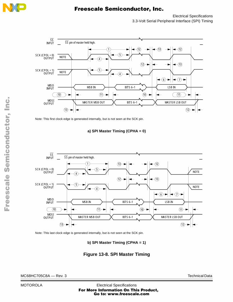
Electrical Specifications3.3-Volt Serial Peripheral Interface (SPI) Timing
F
ree
sca
le S
em
ico
nd
uc
tor,
I
Freescale Semiconductor, Inc.n
c..
.
Figure 13-8. SPI Master Timing
NOTE
Note: This first clock edge is generated internally, but is not seen at the SCK pin.
SS pin of master held high.
MSB IN
SSINPUT
SCK (CPOL = 0)OUTPUT
SCK (CPOL = 1)OUTPUT
MISOINPUT
MOSIOUTPUT
NOTE
4
5
5
1 13 12
4
12 13
BITS 6–1 LSB IN
MASTER MSB OUT BITS 6–1 MASTER LSB OUT
10
13
11 10
12
11
76
NOTE
Note: This last clock edge is generated internally, but is not seen at the SCK pin.
SS pin of master held high.
MSB IN
SSINPUT
SCK (CPOL = 0)OUTPUT
SCK (CPOL = 1)OUTPUT
MISOINPUT
MOSIOUTPUT
NOTE4
5
5
1 13 12
4
13
BITS 6–1 LSB IN
MASTER MSB OUT BITS 6–1 MASTER LSB OUT
10
13
11 10
12
11
76
12
a) SPI Master Timing (CPHA = 0)
b) SPI Master Timing (CPHA = 1)
12
MC68HC705C8A — Rev. 3 Technical Data
MOTOROLA Electrical Specifications For More Information On This Product,
Go to: www.freescale.com

Electrical Specifications
F
ree
sca
le S
em
ico
nd
uc
tor,
I
Freescale Semiconductor, Inc.n
c..
.
Figure 13-9. SPI Slave Timing
Note: Not defined, but normally MSB of character just received
SLAVE
SSINPUT
SCK (CPOL = 0)(INPUT
SCK (CPOL = 1)INPUT
MISOINPUT
MOSIOUTPUT
4
5
5
1 13 12
4
13
MSB IN
BITS 6–1
8
6 10
11
11
12
NOTESLAVE LSB OUT
9
3
LSB IN
2
7
BITS 6–1
MSB OUT
Note: Not defined, but normally LSB of character previously transmitted
SLAVE
SSINPUT
SCK (CPOL = 0)INPUT
SCK (CPOL = 1)INPUT
MISOOUTPUT
MOSIINPUT
4
5
5
1 13 12
4
13
MSB IN
BITS 6–1
8
6 10 11
12
NOTE SLAVE LSB OUT
9
3
LSB IN
2
7
BITS 6–1
MSB OUT
10
a) SPI Slave Timing (CPHA = 0)
b) SPI Slave Timing (CPHA = 1)
Technical Data MC68HC705C8A — Rev. 3
190 Electrical Specifications For More Information On This Product,
Go to: www.freescale.com
F
ree
sca
le S
em
ico
nd
uc
tor,
IFreescale Semiconductor, Inc.
nc
...
Technical Data — MC68HC705C8A
Section 14. Mechanical Specifications
14.1 Contents
14.2 Introduction . . . . . . . . . . . . . . . . . . . . . . . . . . . . . . . . . . . . . . .191
14.3 40-Pin Plastic Dual In-Line Package (PDIP). . . . . . . . . . . . . .192
14.4 40-Pin Ceramic Dual In-Line Package (Cerdip) . . . . . . . . . . .193
14.5 44-Lead Plastic-Leaded Chip Carrier (PLCC) . . . . . . . . . . . .194
14.6 44-Lead Ceramic-Leaded Chip Carrier (CLCC) . . . . . . . . . . .195
14.7 44-Pin Quad Flat Pack (QFP). . . . . . . . . . . . . . . . . . . . . . . . .196
14.8 42-Pin Shrink Dual In-Line Package (SDIP) . . . . . . . . . . . . . .197
14.2 Introduction
Package dimensions available at the time of this publication for the MC68HC705C8A are provided in this section. The packages are:
• 40-pin plastic dual in-line package (PDIP)
• 40-pin ceramic dual-in-line package (cerdip)
• 44-lead plastic-leaded chip carrier (PLCC)
• 44-lead ceramic-leaded chip carrier (CLCC)
• 44-pin quad flat pack (QFP)
• 42-pin shrink dual in-line package (SDIP)
MC68HC705C8A — Rev. 3 Technical Data
MOTOROLA Mechanical Specifications For More Information On This Product,
Go to: www.freescale.com
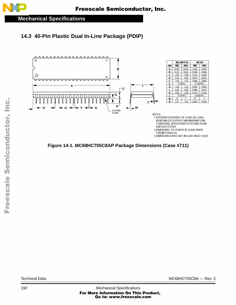
Mechanical Specifications
F
ree
sca
le S
em
ico
nd
uc
tor,
I
Freescale Semiconductor, Inc.n
c..
.
14.3 40-Pin Plastic Dual In-Line Package (PDIP)
Figure 14-1. MC68HC705C8AP Package Dimensions (Case #711)
1 20
40 21
B
AC
SEATINGPLANE
DFGH K
N
M
J
L
DIM MIN MAX MIN MAXINCHESMILLIMETERS
A 51.69 52.45 2.035 2.065B 13.72 14.22 0.540 0.560C 3.94 5.08 0.155 0.200D 0.36 0.56 0.014 0.022F 1.02 1.52 0.040 0.060G 2.54 BSC 0.100 BSCH 1.65 2.16 0.065 0.085J 0.20 0.38 0.008 0.015K 2.92 3.43 0.115 0.135L 15.24 BSC 0.600 BSCM 1°N 0.51 1.02 0.020 0.040
NOTES:1.POSITION TOLERANCE OF LEADS (D), SHALL
BEWITHIN 0.25 (0.010) AT MAXIMUM MATERIALCONDITIONS, IN RELATION TO SEATING PLANEAND EACH OTHER.
2.DIMENSION L TO CENTER OF LEADS WHENFORMED PARALLEL.
3.DIMENSION B DOES NOT INCLUDE MOLD FLASH.
1°0°0°
Technical Data MC68HC705C8A — Rev. 3
192 Mechanical Specifications For More Information On This Product,
Go to: www.freescale.com

Mechanical Specifications40-Pin Ceramic Dual In-Line Package (Cerdip)
F
ree
sca
le S
em
ico
nd
uc
tor,
I
Freescale Semiconductor, Inc.n
c..
.
14.4 40-Pin Ceramic Dual In-Line Package (Cerdip)
Figure 14-2. MC68HC705C8AS Package Dimensions (Case #734A)
M
L
JDIM MIN MAX MIN MAX
MILLIMETERSINCHES
A 2.020 2.096 51.31 53.23B 0.500 0.610 12.70 15.94C 0.160 0.240 4.06 6.09D 0.015 0.022 0.38 0.55F 0.050 0.065 1.27 1.65G 0.100 BSC 2.54 BSCJ 0.008 0.012 0.20 0.30K 0.125 0.160 3.17 4.06L 0.600 BSC 15.24 BSCM 0° 15° 0° 15°N 0.020 0.050 0.51 1.27
Aφ 0.25(0.010) T
T
40 PLD
1
40
20
21
A
B
GF
K
C
N
SEATINGPLANE
DATUMPLANE
MM
MC68HC705C8A — Rev. 3 Technical Data
MOTOROLA Mechanical Specifications For More Information On This Product,
Go to: www.freescale.com

Mechanical Specifications
F
ree
sca
le S
em
ico
nd
uc
tor,
I
Freescale Semiconductor, Inc.n
c..
.
14.5 44-Lead Plastic-Leaded Chip Carrier (PLCC)
Figure 14-3. MC68HC705C8AFN Package Dimensions (Case #777)
-N-
-L- -M-
DY
D
K
VW144
BRK
B
Z
U
X
VIEW D-D
SL-MM0.007(0.180) N ST
SL-MM0.007(0.180) N ST
G1SL-MS0.010 (0.25) N ST
K1
F
H
SL-MM0.007(0.180) N ST
Z
G
G1
R
A
EJ
VIEW S
C
SL-MM0.007(0.180) N ST
SL-MM0.007(0.180) N ST
0.004 (0.10)
-T- SEATINGPLANE
VIEW S
DIM MIN MAX MIN MAX
MILLIMETERSINCHES
A 0.685 0.695 17.40 17.65B 0.685 0.695 17.40 17.65C 0.165 0.180 4.20 4.57E 0.090 0.110 2.29 2.79F 0.013 0.019 0.33 0.48G 0.050 BSC 1.27 BSCH 0.026 0.032 0.66 0.81J 0.020 0.51K 0.025 0.64R 0.650 0.656 16.51 16.66U 0.650 0.656 16.51 16.66V 0.042 0.048 1.07 1.21W 0.042 0.048 1.07 1.21X 0.042 0.056 1.07 1.42Y 0.020 0.50Z 2° 10°
G1 0.610 0.630 15.50 16.00K1 0.040 1.02
SL-MS0.010 (0.25) N ST
SL-MM0.007(0.180) N ST
2° 10°
NOTES:1. DATUMS -L-, -M-, AND -N- ARE DETERMINED
WHERE TOP OF LEAD SHOLDERS EXITSPLASTIC BODY AT MOLD PARTING LINE.
2. DIMENSION G1, TRUE POSITION TO BEMEASURED AT DATUM -T-, SEATING PLANE.
3. DIMENSION R AND U DO NOT INCLUDE MOLDFLASH. ALLOWABLE MOLD FLASH IS 0.010(0.25) PER SIDE.
4. DIMENSIONING AND TOLERANCING PER ANSIY14.5M, 1982.
5. CONTROLLING DIMENSION: INCH.6. THE PACKAGE TOP MAY BE SMALLER THAN
THE PACKAGE BOTTOM BY UP TO 0.012(0.300). DIMENSIONS R AND U ARE DETERMINEDAT THE OUTERMOST EXTREMES OF THEPLASTIC BODY EXCLUSIVE OF THE MOLDFLASH, TIE BAR BURRS, GATE BURRS ANDINTERLEAD FLASH, BUT INCLUDING ANYMISMATCH BETWEEN THE TOP AND BOTTOMOF THE PLASTIC BODY.
7. DIMINSION H DOES NOT INCLUDE DAMBARPROTRUSION OR INTRUSION. THE DAMBARPROTUSION(S) SHALL NOT CAUSE THE HDIMINSION TO BE GREATER THAN 0.037(0.940198). THE DAMBAR INTRUSION(S) SHALLNOT CAUSE THE H DIMINISION TO SMALLERTHAN 0.025 (0.635).
Technical Data MC68HC705C8A — Rev. 3
194 Mechanical Specifications For More Information On This Product,
Go to: www.freescale.com
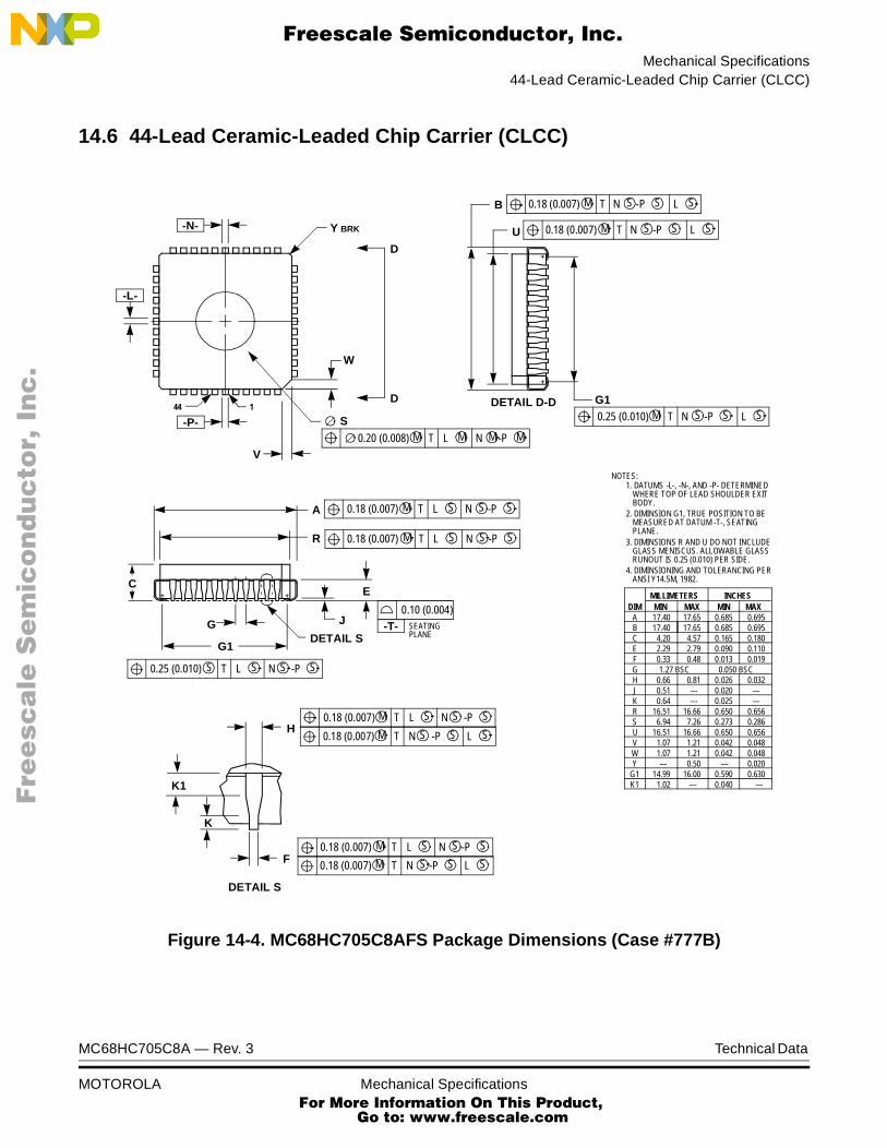
Mechanical Specifications44-Lead Ceramic-Leaded Chip Carrier (CLCC)
F
ree
sca
le S
em
ico
nd
uc
tor,
I
Freescale Semiconductor, Inc.n
c..
.
14.6 44-Lead Ceramic-Leaded Chip Carrier (CLCC)
Figure 14-4. MC68HC705C8AFS Package Dimensions (Case #777B)
17.4017.40
4.202.290.33
0.660.510.64
16.516.94
16.511.071.07---
14.991.02
SLM0.18 (0.007) N -PS ST
B
U
G1
SLM0.18 (0.007) N -PS ST
SLM N -PS STDETAIL D-D
-N-
MLM0.20 (0.008) N -PM MT
-L-
-P-144
V
D
W
S
D
Y BRK
SLM0.18 (0.007) N -PS ST
SLM0.18 (0.007) N -PS ST
0.10 (0.004)SEATINGPLANE
-T-J
E
R
A
G
G1
SLS0.25 (0.010) N -PS ST
DETAIL S
C
SLM0.18 (0.007) N -PS ST
SLM0.18 (0.007) N -PS ST
FSLM0.18 (0.007) N -PS ST
SLM0.18 (0.007) N -PS ST
H
K
K1
DETAIL S
DIM MIN MAX MIN MAXINCHESMILLIMETERS
A 17.65 0.685 0.695B 17.65 0.685 0.695C 4.57 0.165 0.180E 2.79 0.090 0.110F 0.48 0.013 0.019G 1.27 BSC 0.050 BSCH 0.81 0.026 0.032J --- 0.020 ---K --- 0.025 ---R 16.66 0.650 0.656S 7.26 0.273 0.286U 16.66 0.650 0.656V 1.21 0.042 0.048W 1.21 0.042 0.048Y 0.50 --- 0.020
G1 16.00 0.590 0.630K1 --- 0.040 ---
NOTES:1. DATUMS -L-, -N-, AND -P- DETERMINED
WHERE TOP OF LEAD SHOULDER EXITBODY.
2. DIMINSION G1, TRUE POSITION TO BEMEASURED AT DATUM -T-, SEATINGPLANE.
3. DIMINSIONS R AND U DO NOT INCLUDEGLASS MENISCUS. ALLOWABLE GLASSRUNOUT IS 0.25 (0.010) PER SIDE.
4. DIMINSIONING AND TOLERANCING PERANSI Y14.5M, 1982.
0.25 (0.010)
MC68HC705C8A — Rev. 3 Technical Data
MOTOROLA Mechanical Specifications For More Information On This Product,
Go to: www.freescale.com

Mechanical Specifications
F
ree
sca
le S
em
ico
nd
uc
tor,
I
Freescale Semiconductor, Inc.n
c..
.
14.7 44-Pin Quad Flat Pack (QFP)
Figure 14-5. MC68HC705C8AFB Package Dimensions (Case #824A)
NOTES:1. 1. DIMENSIONING AND TOLERANCING PER ANSI
Y14.5M, 1982.2. 2. CONTROLLING DIMENSION: MILLIMETER.3. 3. DATUM PLANE -H- IS LOCATED AT BOTTOM OF
LEAD AND IS COINCIDENT WITH THE LEAD WHERE THE LEAD EXITS THE PLASTIC BODY AT THE BOTTOM OF THE PARTING LINE.
4. 4. DATUMS -A-, -B- AND -D- TO BE DETERMINED AT DATUM PLANE -H-.
5. 5. DIMENSIONS S AND V TO BE DETERMINED AT SEATING PLANE -C-.
6. 6. DIMENSIONS A AND B DO NOT INCLUDE MOLD PROTRUSION. ALLOWABLE PROTRUSION IS 0.25 (0.010) PER SIDE. DIMENSIONS A AND B DO INCLUDE MOLD MISMATCH AND ARE DETERMINED AT DATUM PLANE -H-.
7. 7. DIMENSION D DOES NOT INCLUDE DAMBAR PROTRUSION. ALLOWABLE DAMBAR PROTRUSION SHALL BE 0.08 (0.003) TOTAL IN EXCESS OF THE D DIMENSION AT MAXIMUM MATERIAL CONDITION. DAMBAR CANNOT BE LOCATED ON THE LOWER RADIUS OR THE FOOT.
L
33
34
23
22
44
1 11
12
DETAIL A
-D-
-A-
ASA-BM0.20 (0.008) D SC
SA-BM0.20 (0.008) D SH
0.05 (0.002) A-B
S
BS
A-B
M0.
20 (
0.00
8)D
SC
SA
-BM
0.20
(0.
008)
DS
H
0.05
(0.
002)
A-B
VL
-B-
-C-SEATINGPLANE
M
M
E
HG
C -H- DATUMPLANE
DETAIL C
0.01 (0.004)
M
-H-DATUMPLANE
T
R
KQW
X
DETAIL C
DIM MIN MAX MIN MAXINCHESMILLIMETERS
A 9.90 10.10 0.390 0.398B 9.90 10.10 0.390 0.398C 2.10 2.45 0.083 0.096D 0.30 0.45 0.012 0.018E 2.00 2.10 0.079 0.083F 0.30 0.40 0.012 0.016G 0.80 BSC 0.031 BSCH --- 0.25 --- 0.010J 0.013 0.23 0.005 0.009K 0.65 0.95 0.026 0.037L 8.00 REF 0.315 REFM 5 10 5 10 N 0.13 0.17 0.005 0.007Q 0 7 0 7 R 0.13 0.30 0.005 0.012S 12.95 13.45 0.510 0.530T 0.13 --- 0.005 ---U 0 --- 0 ---V 12.95 13.45 0.510 0.530W 0.40 --- 0.016 ---X 1.6 REF 0.063 REF
DETAIL A
B
B
-A-, -B-, -D-
SA-BM0.20 (0.008) D SC
F
N
SECTION B-B
J
D
BASE METAL
° ° ° °
° ° ° °
° °
Technical Data MC68HC705C8A — Rev. 3
196 Mechanical Specifications For More Information On This Product,
Go to: www.freescale.com

Mechanical Specifications42-Pin Shrink Dual In-Line Package (SDIP)
F
ree
sca
le S
em
ico
nd
uc
tor,
I
Freescale Semiconductor, Inc.n
c..
.
14.8 42-Pin Shrink Dual In-Line Package (SDIP)
Figure 14-6. MC68HC705C8AB Package Dimensions (Case #858)
°
°
°
°
-B-
-A-
C
D 42 PL
FK
G N
J 42 PLM
H
L
! " !
# ! $# !
1 21
42 22
-T-
MC68HC705C8A — Rev. 3 Technical Data
MOTOROLA Mechanical Specifications For More Information On This Product,
Go to: www.freescale.com

Mechanical Specifications
F
ree
sca
le S
em
ico
nd
uc
tor,
I
Freescale Semiconductor, Inc.n
c..
.
Technical Data MC68HC705C8A — Rev. 3
198 Mechanical Specifications For More Information On This Product,
Go to: www.freescale.com
F
ree
sca
le S
em
ico
nd
uc
tor,
IFreescale Semiconductor, Inc.
nc
...
Technical Data — MC68HC705C8A
Section 15. Ordering Information
15.1 Contents
15.2 Introduction . . . . . . . . . . . . . . . . . . . . . . . . . . . . . . . . . . . . . . .199
15.3 MCU Order Numbers . . . . . . . . . . . . . . . . . . . . . . . . . . . . . . .199
15.2 Introduction
This section contains ordering information for the available package types.
15.3 MCU Order Numbers
Table 15-1 lists the MC order numbers.
Table 15-1. MC68HC705C8A Order Numbers
Package Type Temperature Range Order Number
40-pin plastic dual in-line package (PDIP) –40°C to +85°C MC68HC705C8AC(1)P(2)
44-lead plastic-leaded chip carrier (PLCC) –40°C to +85°C MC68HC705C8ACFN(3)
44-lead ceramic-leaded chip carrier (CLCC) –40°C to +85°C MC68HC705C8ACFS(4)
40-pin windowed ceramic DIP (Cerdip) –40°C to +85°C MC68HC705C8ACS(5)
44-pin quad flat pack (QFP) –40°C to +85°C MC68HC705C8ACFB(6)
42-pin shrink dual in-line package (SDIP) –40°C to +85°C MC68HC705C8ACB(7)
1. C = Extended temperature range (–40°C to +85°C)2. P = Plastic dual in-line package (PDIP)3. FN = Plastic-leaded chip carrier (PLCC)4. FS = Ceramic-leaded chip carrier (CLCC)5. S = Windowed ceramic dual in-line package (Cerdip)6. FB = Quad flat pack (QFP)7. B = Shrink dual in-line package (SDIP)
MC68HC705C8A — Rev. 3 Technical Data
MOTOROLA Ordering Information For More Information On This Product,
Go to: www.freescale.com

Ordering Information
F
ree
sca
le S
em
ico
nd
uc
tor,
I
Freescale Semiconductor, Inc.n
c..
.
Technical Data MC68HC705C8A — Rev. 3
200 Ordering Information For More Information On This Product,
Go to: www.freescale.com

F
ree
sca
le S
em
ico
nd
uc
tor,
IFreescale Semiconductor, Inc.
nc
...
Technical Data — MC68HC705C8A
Appendix A. MC68HSC705C8A
A.1 Contents
A.2 Introduction . . . . . . . . . . . . . . . . . . . . . . . . . . . . . . . . . . . . . . .201
A.3 5.0-Volt High-Speed DC Electrical Characteristics. . . . . . . . .202
A.4 3.3-Volt High-Speed DC Electrical Characteristics . . . . . . . .203
A.5 5.0-Volt High-Speed Control Timing . . . . . . . . . . . . . . . . . . . .204
A.6 3.3-Volt High-Speed Control Timing . . . . . . . . . . . . . . . . . . . .204
A.7 5.0-Volt High-Speed SPI Timing . . . . . . . . . . . . . . . . . . . . . .205
A.8 3.3-Volt High-Speed SPI Timing. . . . . . . . . . . . . . . . . . . . . . .207
A.9 Ordering Information. . . . . . . . . . . . . . . . . . . . . . . . . . . . . . . .209
A.2 Introduction
The MC68HSC705C8A is an enhanced, high-speed version of the MC68HC705C8A, featuring a 4-MHz bus speed.
The data in this document, MC68HC705C8A Technical Data Rev. 3, applies to the MC68HSC705C8A with the exceptions given in this appendix.
The computer operating properly (COP) mode bits (CM1 and CM0 in the COP control register) select the timeout period of the programmable COP watchdog, as shown in Table A-1. See Figure 5-3. Programmable COP Control Register (COPCR).
MC68HC705C8A — Rev. 3 Technical Data
MOTOROLA MC68HSC705C8A For More Information On This Product,
Go to: www.freescale.com

MC68HSC705C8A
F
ree
sca
le S
em
ico
nd
uc
tor,
I
Freescale Semiconductor, Inc.n
c..
.
A.3 5.0-Volt High-Speed DC Electrical Characteristics
Table A-1. Programmable COP Timeout Period Selection
CM1:CM0COP
Timeout Rate
Programmable COP Timeout Period
fOSC = 8.0 MHzfOP = 4.0 MHz
fOSC = 4.0 MHzfOP = 2.0 MHz
fOSC = 3.5795 MHzfOP = 1.7897 MHz
fOSC = 2.0 MHzfOP = 1.0 MHz
00 fOP ÷ 215 8.192 ms 16.38 ms 18.31 ms 32.77 ms
01 fOP ÷ 217 32.77 ms 65.54 ms 73.24 ms 131.07 ms
10 fOP ÷ 219 131.07 ms 262.14 ms 292.95 ms 524.29 ms
11 fOP ÷ ÷221 524.29 ms 1.048 s 1.172 s 2.097 s
Characteristic(1)
1. VDD = 5 V ± 10%; VSS = 0 Vdc, TA = TL to TH, unless otherwise noted
Symbol Min Typ(2)
2. Typical values reflect average measurements at midpoint of voltage range at 25°C.
Max Unit
Output high voltageILoad = –0.8 mA
PA7–PA0, PB7–PB0, PC6–PC0, TCMPILoad = –1.6 mA
PD4–PD1ILoad = –5.0 mA
PC7
VOH VDD – 0.8—
—
—
—
—
—
V
Output low voltageILoad = 1.6 mA
PA7–PA0, PB7–PB0, PC6–PC0, PD4–PD1ILoad = 20 mA
PC7
VOL —
—
—
—
0.4
0.4
V
Supply current(3)
Run(4)
Wait(5)
Stop(6)
25°C–40°C to +85°C
3. IDD measured with port B pullup devices disabled.4. Run (operating) IDD measured using external square wave clock source (fOSC = 8.0 MHz). All inputs 0.2 V from rail. No dc
loads. Less than 50 pF on all outputs. CL = 20 pF on OSC2. OSC2 capacitance linearly affects run IDD.5. Wait IDD measured using external square wave clock source (fOSC = 8.0 MHz). All inputs 0.2 V from rail. No dc loads. Less
than 50 pF on all outputs. CL = 20 pF on OSC2. VIL = 0.2 V, VIH = VDD – 0.2 V. All ports configured as inputs. SPI and SCIdisabled. If SPI and SCI enabled, add 10% current draw. OSC2 capacitance linearly affects wait IDD.
6. Stop IDD measured with OSC1 = VDD. All ports configured as inputs. VIL = 0.2 V, VIH = VDD – 0.2 V.
IDD
——
——
5.922.27
52.0
147.0
5050
mAmA
µAµA
Technical Data MC68HC705C8A — Rev. 3
202 MC68HSC705C8A For More Information On This Product,
Go to: www.freescale.com

MC68HSC705C8A
F
ree
sca
le S
em
ico
nd
uc
tor,
I
Freescale Semiconductor, Inc.n
c..
.
A.4 3.3-Volt High-Speed DC Electrical Characteristics
Characteristic(1)
1. VDD = 3.3 V ± 10%; VSS = 0 Vdc, TA = TL to TH, unless otherwise noted
Symbol Min Typ(2)
2. Typical values reflect average measurements at midpoint of voltage range at 25°C.
Max Unit
Output high voltageILoad = –0.2 mA
PA7–PA0, PB7–PB0, PC6–PC0, TCMPILoad = –0.4 mA
PD4–PD1ILoad = –1.5 mA
PC7
VOH VDD – 0.3—
—
—
—
—
—
V
Output low voltageILoad = 0.4 mA
PA7–PA0, PB7–PB0, PC6–PC0, PD4–PD1ILoad = 6.0 mA
PC7
VOL —
—
—
—
0.3
0.3
V
Supply current(3)
Run(4)
Wait(5)
Stop(6)
3. IDD measured with port B pullup devices disabled.4. Run (operating) IDD measured using external square wave clock source (fOSC = 4.2 MHz). All inputs 0.2 V from rail. No dc
loads. Less than 50 pF on all outputs. CL = 20 pF on OSC2. OSC2 capacitance linearly affects run IDD.5. Wait IDD measured using external square wave clock source (fOSC = 4.2 MHz). All inputs 0.2 V from rail. No dc loads. Less
than 50 pF on all outputs. CL = 20 pF on OSC2. VIL = 0.2 V, VIH = VDD – 0.2 V. All ports configured as inputs. SPI and SCIdisabled. If SPI and SCI enabled, add 10% current draw. OSC2 capacitance linearly affects wait IDD.
6. Stop IDD measured with OSC1 = VDD. All ports configured as inputs. VIL = 0.2 V; VIH = VDD – 0.2 V.
IDD———
1.910.915
2.0
6.02.020
mAmAµA
MC68HC705C8A — Rev. 3 Technical Data
MOTOROLA MC68HSC705C8A For More Information On This Product,
Go to: www.freescale.com

MC68HSC705C8A
F
ree
sca
le S
em
ico
nd
uc
tor,
I
Freescale Semiconductor, Inc.n
c..
.
A.5 5.0-Volt High-Speed Control Timing
A.6 3.3-Volt High-Speed Control Timing
Characteristic(1) Symbol Min Max Unit
Oscillator frequencyCrystal oscillatorExternal clock
fOSC —dc
8.08.0
MHz
Internal operating frequency (fOSC ÷ 2)Crystal oscillatorExternal clock
fOP —dc
4.04.0
MHz
Cycle time tCYC 250 — ns
Input capture pulse width tTH, tTL 65 — ns
Interrupt pulse width low (edge-triggered) tILIH 65 — ns
OSC1 pulse width tOH, tOL 45 — ns
1. VDD = 5 V ± 10%; VSS = 0 Vdc, TA = TL to TH, unless otherwise noted
Characteristic(1) Symbol Min Max Unit
Oscillator frequencyCrystal oscillatorExternal clock
fOSC —dc
4.04.0
MHz
Internal operating frequency (fOSC ÷ 2)Crystal oscillatorExternal clock
fOP —dc
2.02.0
MHz
Cycle time tCYC 476 — ns
Input capture pulse width tTH, tTL 125 — ns
Interrupt pulse width low (edge-triggered) tILIH 125 — ns
OSC1 pulse width tOH, tOL 90 — ns
1. VDD = 3.3 V ± 10%; VSS = 0 Vdc, TA = TL to TH, unless otherwise noted
Technical Data MC68HC705C8A — Rev. 3
204 MC68HSC705C8A For More Information On This Product,
Go to: www.freescale.com

MC68HSC705C8A
F
ree
sca
le S
em
ico
nd
uc
tor,
I
Freescale Semiconductor, Inc.n
c..
.
A.7 5.0-Volt High-Speed SPI Timing
Diagram
Number(1) Characteristic(2) Symbol Min Max Unit
Operating frequencyMasterSlave
fOP(S)fOP(S)
dcdc
0.54.0
fOPMHz
1Cycle time
MasterSlave
tCYC(M)tCYC(S)
2.0250
——
tCYC
ns
2Enable lead time
MasterSlave
tLead(M)tLead(S)
Note (3)
125——
ns
3Enable lag time
MasterSlave
tLag(M)tLag(S)
Note(2)
375——
ns
4Clock (SCK) high time
MasterSlave
tW(SCKH)M
tW(SCKH)S
17095
——
ns
5Clock (SCK) low time
MasterSlave
tW(SCKL)MtW(SCKL)S
17095
——
ns
6Data setup time (inputs)
MasterSlave
tSU(M)tSU(S)
5050
——
ns
7Data hold time (inputs)
MasterSlave
tH(M)tH(S)
5050
——
ns
8 Access time(4)
SlavetA 0 60 ns
9 Disable time(5)
SlavetDIS — 120 ns
10Data valid time
Master (before capture edge)
Slave (after enable edge)(6)tV(M)tV(S)
0.25—
—120
tCYC(M)ns
Continued
MC68HC705C8A — Rev. 3 Technical Data
MOTOROLA MC68HSC705C8A For More Information On This Product,
Go to: www.freescale.com

MC68HSC705C8A
F
ree
sca
le S
em
ico
nd
uc
tor,
I
Freescale Semiconductor, Inc.n
c..
.
11Data hold time (outputs)
Master (after capture edge)Slave (after enable edge)
tHO(M)tHO(S)
0.250
——
tCYC(M)
ns
12Rise time(7)
SPI outputs (SCK, MOSI, MISO)SPI inputs (SCK, MOSI, MISO, SS)
tRMtRS
——
502.0
nsµs
13Fall time(8)
SPI outputs (SCK, MOSI, MISO)SPI inputs (SCK, MOSI, MISO, SS)
tFMtFS
——
502.0
nsµs
1. Diagram numbers refer to dimensions in Figure 13-8. SPI Master Timing and Figure 13-9. SPI Slave Timing.2. VDD = 5 V ± 10%; VSS = 0 Vdc, TA = TL to TH, unless otherwise noted3. Signal production depends on software.4. Time to data active from high-impedance state5. Hold time to high-impedance state6. With 200 pF on all SPI pins.7. 20% of VDD to 70% of VDD; CL = 200 pF8. 70% of VDD to 20% of VDD; CL = 200 pF
Diagram
Number(1) Characteristic(2) Symbol Min Max Unit
Technical Data MC68HC705C8A — Rev. 3
206 MC68HSC705C8A For More Information On This Product,
Go to: www.freescale.com

MC68HSC705C8A
F
ree
sca
le S
em
ico
nd
uc
tor,
I
Freescale Semiconductor, Inc.n
c..
.
A.8 3.3-Volt High-Speed SPI Timing
Diagram
Number(1) Characteristic(2) Symbol Min Max Unit
Operating frequencyMasterSlave
fOP(S)
fOP(S)
dcdc
0.52.1
fOPMHz
1Cycle time
MasterSlave
tCYC(M)tCYC(S)
2.0480
——
tCYCns
2Enable lead time
MasterSlave
tLead(M)tLead(S)
Note (3)
240——
ns
3Enable lag time
MasterSlave
tLag(M)
tLag(S)
Note(2)
720——
ns
4Clock (SCK) high time
MasterSlave
tW(SCKH)MtW(SCKH)S
340190
——
ns
5Clock (SCK) low time
MasterSlave
tW(SCKL)MtW(SCKL)S
340190
——
ns
6Data setup time (inputs)
MasterSlave
tSU(M)tSU(S)
100100
——
ns
7Data hold time (inputs)
MasterSlave
tH(M)tH(S)
100100
——
ns
8 Access time(4)
SlavetA 0 120
ns
9 Disable time(5)
SlavetDIS — 240
ns
10Data valid time
Master (before capture edge)
Slave (after enable edge)(6)tV(M)
tV(S)
0.25—
—240
tCYC(M)ns
Continued
MC68HC705C8A — Rev. 3 Technical Data
MOTOROLA MC68HSC705C8A For More Information On This Product,
Go to: www.freescale.com

MC68HSC705C8A
F
ree
sca
le S
em
ico
nd
uc
tor,
I
Freescale Semiconductor, Inc.n
c..
.
11Data hold time (outputs)
Master (after capture edge)Slave (after enable edge)
tHO(M)tHO(S)
0.250
——
tCYC(M)
ns
12Rise time(7)
SPI outputs (SCK, MOSI, MISO)SPI inputs (SCK, MOSI, MISO, SS)
tRMtRS
——
1002.0
nsµs
13Fall time(8)
SPI outputs (SCK, MOSI, MISO)SPI inputs (SCK, MOSI, MISO, SS)
tFMtFS
——
1002.0
nsµs
1. Diagram numbers refer to dimensions in Figure 13-8. SPI Master Timing and Figure 13-9. SPI Slave Timing.2. VDD = 3.3 V ± 10%; VSS = 0 Vdc, TA = TL to TH, unless otherwise noted3. Signal production depends on software.4. Time to data active from high-impedance state5. Hold time to high-impedance state6. With 200 pF on all SPI pins7. 20% of VDD to 70% of VDD; CL = 200 pF8. 70% of VDD to 20% of VDD; CL = 200 pF
Diagram
Number(1) Characteristic(2) Symbol Min Max Unit
Technical Data MC68HC705C8A — Rev. 3
208 MC68HSC705C8A For More Information On This Product,
Go to: www.freescale.com

MC68HSC705C8A
F
ree
sca
le S
em
ico
nd
uc
tor,
I
Freescale Semiconductor, Inc.n
c..
.
A.9 Ordering Information
Table A-2 provides ordering information for the MC68HSC705C8A.
Table A-2. MC68HSC705C8A Order Numbers
Package Type Temperature Range Order Number
40-pin plastic dual in-line package (PDIP) –40°C to +85°C MC68HSC705C8AC(1)P(2)
44-lead plastic-leaded chip carrier (PLCC) –40°C to +85°C MC68HSC705C8ACFN(3)
44-lead ceramic-leaded chip carrier (CLCC) –40°C to +85°C MC68HSC705C8ACFS(4)
40-pin ceramic DIP (cerdip) –40°C to +85°C MC68HSC705C8ACS(5)
44-pin quad flat pack (QFP) –40°C to +85°C MC68HSC705C8ACFB(6)
42-pin shrink dual in-line package (SDIP) –40°C to +85°C MC68HSC705C8ACB(7)
1. C = Extended temperature range (–40°C to +85°C)2. P = Plastic dual in-line package (PDIP)3. FN = Plastic-leaded chip carrier (PLCC)4. FS = Ceramic-leaded chip carrier (CLCC)5. S = Windowed ceramic dual in-line package (cerdip)6. FB = Quad flat pack (QFP)7. B = Shrink dual in-line package (SDIP)
MC68HC705C8A — Rev. 3 Technical Data
MOTOROLA MC68HSC705C8A For More Information On This Product,
Go to: www.freescale.com

MC68HSC705C8A
F
ree
sca
le S
em
ico
nd
uc
tor,
I
Freescale Semiconductor, Inc.n
c..
.
Technical Data MC68HC705C8A — Rev. 3
210 MC68HSC705C8A For More Information On This Product,
Go to: www.freescale.com
F
ree
sca
le S
em
ico
nd
uc
tor,
IFreescale Semiconductor, Inc.
nc
...
Technical Data — MC68HC705C8A
Index
A
accumulator (A) . . . . . . . . . . . . . . . . . . . . . . . . . . . . . 45, 154, 155, 158
addressing modes . . . . . . . . . . . . . . . . . . . . . . . . . . . . . . . . . . . . . . 154
arithmetic/logic unit (ALU) . . . . . . . . . . . . . . . . . . . . . . . . . . . . . . . . . 48
B
block diagram . . . . . . . . . . . . . . . . . . . . . . . . . . . . . . . . . . . . . . . . . . 24
bootloader ROM . . . . . . . . . . . . . . . . . . . . . . . . . . . . . . . . . . . . . . . . 37
C
C bit . . . . . . . . . . . . . . . . . . . . . . . . . . . . . . . . . . . . . . . . . . . . . . . . . 160
condition code register (CCR) . . . . . . . . . . . . . . . . . . . . . . . . . . 47, 160
COP watchdog (non-programmable)diagram . . . . . . . . . . . . . . . . . . . . . . . . . . . . . . . . . . . . . . . . . . . . 67flowchart. . . . . . . . . . . . . . . . . . . . . . . . . . . . . . . . . . . . . . . . . . . . 73in stop mode. . . . . . . . . . . . . . . . . . . . . . . . . . . . . . . . . . . . . . . . . 73reset . . . . . . . . . . . . . . . . . . . . . . . . . . . . . . . . . . . . . . . . . . . . . . . 66timeout period formula . . . . . . . . . . . . . . . . . . . . . . . . . . . . . . . . . 66when clock monitor enabled. . . . . . . . . . . . . . . . . . . . . . . . . . . . . 73
COP watchdog (programmable)COP control register (COPCR) . . . . . . . . . . . . . . . . . . . . . . . . . . 64COP reset register (COPRST) . . . . . . . . . . . . . . . . . . . . . . . . . . . 64diagram . . . . . . . . . . . . . . . . . . . . . . . . . . . . . . . . . . . . . . . . . . . . 63flowchart. . . . . . . . . . . . . . . . . . . . . . . . . . . . . . . . . . . . . . . . . . . . 71in stop mode. . . . . . . . . . . . . . . . . . . . . . . . . . . . . . . . . . . . . . . . . 71reset . . . . . . . . . . . . . . . . . . . . . . . . . . . . . . . . . . . . . . . . . . . . . . . 63timeout period selection . . . . . . . . . . . . . . . . . . . . . . . . . . . . . . . . 66
MC68HC705C8A — Rev. 3 Technical Data
MOTOROLA Index For More Information On This Product,
Go to: www.freescale.com

Index
F
ree
sca
le S
em
ico
nd
uc
tor,
I
Freescale Semiconductor, Inc.n
c..
.
CPUinstruction set summary . . . . . . . . . . . . . . . . . . . . . . . . . . . . . . . 164instruction types . . . . . . . . . . . . . . . . . . . . . . . . . . . . . . . . . . . . . 157opcode map . . . . . . . . . . . . . . . . . . . . . . . . . . . . . . . . . . . . . . . . 170programming model . . . . . . . . . . . . . . . . . . . . . . . . . . . . . . . . . . . 44registers . . . . . . . . . . . . . . . . . . . . . . . . . . . . . . . . . . . . . . . . . . . . 44
CPU registers . . . . . . . . . . . . . . . . . . . . . . . . . . . . . . . . . 155, 158, 163accumulator (A) . . . . . . . . . . . . . . . . . . . . . . . . . . . . . 154, 155, 158condition code register (CCR) . . . . . . . . . . . . . . . . . . . . . . . . . . 160index register (X) . . . . . . . . . . . . . . . . . . . . . . . . 154, 155, 156, 158program counter (PC) . . . . . . . . . . . . . . . . . . . . . . . . . . . . 157, 160
D
data-retention mode . . . . . . . . . . . . . . . . . . . . . . . . . . . . . . . . . . . . . 75
E
electrical specifications . . . . . . . . . . . . . . . . . . . . . . . . . . . . . . . . . . 171control timing . . . . . . . . . . . . . . . . . . . . . . . . . . . . . . . . . . . . . . . 181DC electrical characteristics. . . . . . . . . . . . . . . . . . . . . . . . . . . . 176power considerations . . . . . . . . . . . . . . . . . . . . . . . . . . . . . . . . . 174
electrical specifications (high-speed part)control timing . . . . . . . . . . . . . . . . . . . . . . . . . . . . . . . . . . . . . . . 204DC electrical characteristics. . . . . . . . . . . . . . . . . . . . . . . . . . . . 202ordering information . . . . . . . . . . . . . . . . . . . . . . . . . . . . . . . . . . 209SPI timing. . . . . . . . . . . . . . . . . . . . . . . . . . . . . . . . . . . . . . . . . . 205
EPROM/OTPROM (PROM) . . . . . . . . . . . . . . . . . . . . . . . . . . . 37, 103control registers . . . . . . . . . . . . . . . . . . . . . . . . . . . . . . . . . . . . . 116EPROM erasing . . . . . . . . . . . . . . . . . . . . . . . . . . . . . . . . . . . . . 119mask option register 1 (MOR1) . . . . . . . . . . . . . . . . . . . . . . . . . 117mask option register 2 (MOR2) . . . . . . . . . . . . . . . . . . . . . . . . . 118option register (option) . . . . . . . . . . . . . . . . . . . . . . . . . . . . . . . . 116preprogramming steps . . . . . . . . . . . . . . . . . . . . . . . . . . . . . . . . 110program register (PROG). . . . . . . . . . . . . . . . . . . . . . . . . . . . . . 109programming . . . . . . . . . . . . . . . . . . . . . . . . . . . . . . . . . . . . . . . 104
MC68HC05PGMR programmer board . . . . . . . . . . . . . . . . . 104programming circuit . . . . . . . . . . . . . . . . . . . . . . . . . . . . . . . . . . 106
Technical Data MC68HC705C8A — Rev. 3
212 Index For More Information On This Product,
Go to: www.freescale.com

Index
F
ree
sca
le S
em
ico
nd
uc
tor,
I
Freescale Semiconductor, Inc.n
c..
.
programming flowchart. . . . . . . . . . . . . . . . . . . . . . . . . . . . . . . . 105programming routines . . . . . . . . . . . . . . . . . . . . . . . . . . . . 108, 111
F
features . . . . . . . . . . . . . . . . . . . . . . . . . . . . . . . . . . . . . . . . . . . . . . . 22
H
high-speed part (MC68HSC705C8A) . . . . . . . . . . . . . . . . . . . . . . . 201
I
I/O . . . . . . . . . . . . . . . . . . . . . . . . . . . . . . . . . . . . . . . . . . . . . . . . 36, 77data direction register A (DDRA) . . . . . . . . . . . . . . . . . . . . . . . . . 79data direction register B (DDRB) . . . . . . . . . . . . . . . . . . . . . . . . . 82data direction register C (DDRC) . . . . . . . . . . . . . . . . . . . . . . . . . 86port A . . . . . . . . . . . . . . . . . . . . . . . . . . . . . . . . . . . . . . . . . . . . . . 78port A data register (PORTA). . . . . . . . . . . . . . . . . . . . . . . . . . . . 78port A I/O logic . . . . . . . . . . . . . . . . . . . . . . . . . . . . . . . . . . . . . . . 80port A pin functions . . . . . . . . . . . . . . . . . . . . . . . . . . . . . . . . . . . 80port B . . . . . . . . . . . . . . . . . . . . . . . . . . . . . . . . . . . . . . . . . . . . . . 81port B data register (PORTB). . . . . . . . . . . . . . . . . . . . . . . . . . . . 81port B I/O logic . . . . . . . . . . . . . . . . . . . . . . . . . . . . . . . . . . . . . . . 83port B pin functions . . . . . . . . . . . . . . . . . . . . . . . . . . . . . . . . . . . 84port C . . . . . . . . . . . . . . . . . . . . . . . . . . . . . . . . . . . . . . . . . . . . . . 85port C data register . . . . . . . . . . . . . . . . . . . . . . . . . . . . . . . . . . . 85port C I/O logic . . . . . . . . . . . . . . . . . . . . . . . . . . . . . . . . . . . . . . . 87port C pin functions . . . . . . . . . . . . . . . . . . . . . . . . . . . . . . . . . . . 87port D . . . . . . . . . . . . . . . . . . . . . . . . . . . . . . . . . . . . . . . . . . . . . . 88
I/O bitsC bit . . . . . . . . . . . . . . . . . . . . . . . . . . . . . . . . . . . . . . . . . . . . . . 160
I/O register summary . . . . . . . . . . . . . . . . . . . . . . . . . . . . . . . . . . . . . 39
index register (X) . . . . . . . . . . . . . . . . . . . . . . . . 45, 154, 155, 156, 158
instruction set . . . . . . . . . . . . . . . . . . . . . . . . . . . . . . . . . . . . . . . . . 153addressing modes . . . . . . . . . . . . . . . . . . . . . . . . . . . . . . . . . . . 154instruction set summary . . . . . . . . . . . . . . . . . . . . . . . . . . . . . . . 164instruction types . . . . . . . . . . . . . . . . . . . . . . . . . . . . . . . . . . . . . 157opcode map . . . . . . . . . . . . . . . . . . . . . . . . . . . . . . . . . . . . . . . . 170
MC68HC705C8A — Rev. 3 Technical Data
MOTOROLA Index For More Information On This Product,
Go to: www.freescale.com

Index
F
ree
sca
le S
em
ico
nd
uc
tor,
I
Freescale Semiconductor, Inc.n
c..
.
interrupt processing . . . . . . . . . . . . . . . . . . . . . . . . . . . . . . . . . . . . . . 57flowchart. . . . . . . . . . . . . . . . . . . . . . . . . . . . . . . . . . . . . . . . . . . . 59reset/interrupt vector addresses. . . . . . . . . . . . . . . . . . . . . . . . . . 57stacking order. . . . . . . . . . . . . . . . . . . . . . . . . . . . . . . . . . . . . . . . 58
interruptsexternal interrupt (IRQ) . . . . . . . . . . . . . . . . . . . . . . . . . . . . . . . . 51
internal function diagram . . . . . . . . . . . . . . . . . . . . . . . . . . . . 52timing diagram . . . . . . . . . . . . . . . . . . . . . . . . . . . . . . . . . . . . 52
interrupt sources . . . . . . . . . . . . . . . . . . . . . . . . . . . . . . . . . . . . . 50masking . . . . . . . . . . . . . . . . . . . . . . . . . . . . . . . . . . . . . . . . . . . . 50port B interrupts . . . . . . . . . . . . . . . . . . . . . . . . . . . . . . . . . . . . . . 53
enabling . . . . . . . . . . . . . . . . . . . . . . . . . . . . . . . . . . . . . . . . . 53port B I/O logic . . . . . . . . . . . . . . . . . . . . . . . . . . . . . . . . . . . . 54
SCI interrupts . . . . . . . . . . . . . . . . . . . . . . . . . . . . . . . . . . . . . . . . 55software interrupt . . . . . . . . . . . . . . . . . . . . . . . . . . . . . . . . . . . . . 50sources. . . . . . . . . . . . . . . . . . . . . . . . . . . . . . . . . . . . . . . . . . . . . 49SPI interrupts . . . . . . . . . . . . . . . . . . . . . . . . . . . . . . . . . . . . . . . . 56timer interrupts . . . . . . . . . . . . . . . . . . . . . . . . . . . . . . . . . . . . . . . 55
IRQ pin . . . . . . . . . . . . . . . . . . . . . . . . . . . . . . . . . . . . . . . . . . . . . . . 32
J
junction temperature . . . . . . . . . . . . . . . . . . . . . . . . . . . . . . . . . . . . 174
L
low-power modes . . . . . . . . . . . . . . . . . . . . . . . . . . . . . . . . . . . . . . . 69data-retention mode. . . . . . . . . . . . . . . . . . . . . . . . . . . . . . . . . . . 75stop mode
non-programmable COP in stop mode flowchart . . . . . . . . . . 74non-programmable COP watchdog in stop mode. . . . . . . . . . 73programmable COP in stop mode flowchart. . . . . . . . . . . . . . 72programmable COP watchdog in stop mode . . . . . . . . . . . . . 71SCI during stop mode. . . . . . . . . . . . . . . . . . . . . . . . . . . . . . . 71SPI during stop mode . . . . . . . . . . . . . . . . . . . . . . . . . . . . . . . 71stop/wait mode function flowchart. . . . . . . . . . . . . . . . . . . . . . 70
wait mode. . . . . . . . . . . . . . . . . . . . . . . . . . . . . . . . . . . . . . . . . . . 73non-programmable COP watchdog in wait mode . . . . . . . . . . 75programmable COP watchdog in wait mode . . . . . . . . . . . . . 75
Technical Data MC68HC705C8A — Rev. 3
214 Index For More Information On This Product,
Go to: www.freescale.com

Index
F
ree
sca
le S
em
ico
nd
uc
tor,
I
Freescale Semiconductor, Inc.n
c..
.
M
mask option registers . . . . . . . . . . . . . . . . . . . . . . . . . . . . 23, 117, 118
MC68HSC705C8A (high-speed part) . . . . . . . . . . . . . . . . . . . . . . . 201control timing . . . . . . . . . . . . . . . . . . . . . . . . . . . . . . . . . . . . . . . 204DC electrical characteristics. . . . . . . . . . . . . . . . . . . . . . . . . . . . 202ordering information . . . . . . . . . . . . . . . . . . . . . . . . . . . . . . . . . . 209programmable COP timeout period selection . . . . . . . . . . . . . . 202SPI timing. . . . . . . . . . . . . . . . . . . . . . . . . . . . . . . . . . . . . . . . . . 205
mechanical specifications . . . . . . . . . . . . . . . . . . . . . . . . . . . . . . . . 191
memorybootloader ROM. . . . . . . . . . . . . . . . . . . . . . . . . . . . . . . . . . . . . . 37I/O . . . . . . . . . . . . . . . . . . . . . . . . . . . . . . . . . . . . . . . . . . . . . . . . 36I/O register summary . . . . . . . . . . . . . . . . . . . . . . . . . . . . . . . . . . 39memory map . . . . . . . . . . . . . . . . . . . . . . . . . . . . . . . . . . . . . 35, 38PROM (EPROM/OTPROM) . . . . . . . . . . . . . . . . . . . . . . . . . . . . . 37RAM . . . . . . . . . . . . . . . . . . . . . . . . . . . . . . . . . . . . . . . . . . . . . . . 36
memory map . . . . . . . . . . . . . . . . . . . . . . . . . . . . . . . . . . . . . . . . 35, 38
O
on-chip memory. . . . . . . . . . . . . . . . . . . . . . . . . . . . . . . . . . . . . . . . . 35
opcode map. . . . . . . . . . . . . . . . . . . . . . . . . . . . . . . . . . . . . . . . . . . 170
option register . . . . . . . . . . . . . . . . . . . . . . . . . . . . . . . . . . . . . . . . . . 23
ordering information. . . . . . . . . . . . . . . . . . . . . . . . . . . . . . . . . . . . . 199order numbers . . . . . . . . . . . . . . . . . . . . . . . . . . . . . . . . . . . . . . 199
OSC1 pin. . . . . . . . . . . . . . . . . . . . . . . . . . . . . . . . . . . . . . . . . . . . . . 30
OSC2 pin. . . . . . . . . . . . . . . . . . . . . . . . . . . . . . . . . . . . . . . . . . . . . . 30
oscillatorceramic resonator . . . . . . . . . . . . . . . . . . . . . . . . . . . . . . . . . . . . 30crystal resonator . . . . . . . . . . . . . . . . . . . . . . . . . . . . . . . . . . . . . .30external clock signal. . . . . . . . . . . . . . . . . . . . . . . . . . . . . . . . . . . 30
MC68HC705C8A — Rev. 3 Technical Data
MOTOROLA Index For More Information On This Product,
Go to: www.freescale.com

Index
F
ree
sca
le S
em
ico
nd
uc
tor,
I
Freescale Semiconductor, Inc.n
c..
.
P
pin assignments. . . . . . . . . . . . . . . . . . . . . . . . . . . . . . . . . . . . . . . . . 26
port A. . . . . . . . . . . . . . . . . . . . . . . . . . . . . . . . . . . . . . . . . . . . . . 33, 78data direction register A (DDRA) . . . . . . . . . . . . . . . . . . . . . . . . . 79port A data register (PORT A) . . . . . . . . . . . . . . . . . . . . . . . . . . . 78port A I/O logic . . . . . . . . . . . . . . . . . . . . . . . . . . . . . . . . . . . . . . . 80port A pin functions . . . . . . . . . . . . . . . . . . . . . . . . . . . . . . . . . . . 80
port B. . . . . . . . . . . . . . . . . . . . . . . . . . . . . . . . . . . . . . . . . . . . . . 33, 81data direction register B (DDRB) . . . . . . . . . . . . . . . . . . . . . . . . . 82port B data register (PORTB). . . . . . . . . . . . . . . . . . . . . . . . . . . . 81port B I/O logic . . . . . . . . . . . . . . . . . . . . . . . . . . . . . . . . . . . . . . . 83port B pin functions . . . . . . . . . . . . . . . . . . . . . . . . . . . . . . . . . . . 84
port C. . . . . . . . . . . . . . . . . . . . . . . . . . . . . . . . . . . . . . . . . . . . . . 33, 85data direction register C (DDRC) . . . . . . . . . . . . . . . . . . . . . . . . . 86port C data register . . . . . . . . . . . . . . . . . . . . . . . . . . . . . . . . . . . 85port C I/O logic . . . . . . . . . . . . . . . . . . . . . . . . . . . . . . . . . . . . . . . 87port C pin functions . . . . . . . . . . . . . . . . . . . . . . . . . . . . . . . . . . .87
port D. . . . . . . . . . . . . . . . . . . . . . . . . . . . . . . . . . . . . . . . . . . . . . 33, 88
power dissipation. . . . . . . . . . . . . . . . . . . . . . . . . . . . . . . . . . . . . . . 174
program counter (PC) . . . . . . . . . . . . . . . . . . . . . . . . . . . . 46, 157, 160
programmable options. . . . . . . . . . . . . . . . . . . . . . . . . . . . . . . . . . . . 23
programming model. . . . . . . . . . . . . . . . . . . . . . . . . . . . . . . . . . . . . . 44
PROM (EPROM/OTPROM) . . . . . . . . . . . . . . . . . . . . . . . . . . . . . . . 37
R
RAM. . . . . . . . . . . . . . . . . . . . . . . . . . . . . . . . . . . . . . . . . . . . . . . . . . 36
registersI/O register summary . . . . . . . . . . . . . . . . . . . . . . . . . . . . . . . . . . 39
reset and interrupt processing flowchart . . . . . . . . . . . . . . . . . . . . . . 59
RESET pin. . . . . . . . . . . . . . . . . . . . . . . . . . . . . . . . . . . . . . . . . . . . . 32
resets. . . . . . . . . . . . . . . . . . . . . . . . . . . . . . . . . . . . . . . . . . . . . . . . . 61clock monitor reset . . . . . . . . . . . . . . . . . . . . . . . . . . . . . . . . . 65, 67
with STOP instructions . . . . . . . . . . . . . . . . . . . . . . . . . . . . . . 67
Technical Data MC68HC705C8A — Rev. 3
216 Index For More Information On This Product,
Go to: www.freescale.com

Index
F
ree
sca
le S
em
ico
nd
uc
tor,
I
Freescale Semiconductor, Inc.n
c..
.
COP watchdog resets . . . . . . . . . . . . . . . . . . . . . . . . . . . . . . . . . 62non-programmable . . . . . . . . . . . . . . . . . . . . . . . . . . . . . . . . . 66non-programmable COP watchdog diagram . . . . . . . . . . . . . 67programmable. . . . . . . . . . . . . . . . . . . . . . . . . . . . . . . . . . . . . 63programmable COP watchdog diagram . . . . . . . . . . . . . . . . . 63
enabling both programmable and non-programmable COPs . . . 65external reset . . . . . . . . . . . . . . . . . . . . . . . . . . . . . . . . . . . . . . . . 62power-on reset (POR) . . . . . . . . . . . . . . . . . . . . . . . . . . . . . . . . . 62reset sources . . . . . . . . . . . . . . . . . . . . . . . . . . . . . . . . . . . . . . . . 61
ROM (bootloader) . . . . . . . . . . . . . . . . . . . . . . . . . . . . . . . . . . . . . . . 37
S
serial communications interface (SCI). . . . . . . . . . . . . . . . . . . . . . . 121baud rate generator clock prescaling . . . . . . . . . . . . . . . . . . . . . 136baud rate register (baud) . . . . . . . . . . . . . . . . . . . . . . . . . . . . . . 136baud rate selection. . . . . . . . . . . . . . . . . . . . . . . . . . . . . . . . . . . 137baud rate selection examples . . . . . . . . . . . . . . . . . . . . . . . . . . 138during stop mode . . . . . . . . . . . . . . . . . . . . . . . . . . . . . . . . . . . . . 71features . . . . . . . . . . . . . . . . . . . . . . . . . . . . . . . . . . . . . . . . . . . 122SCI control register 1 (SCCR1) . . . . . . . . . . . . . . . . . . . . . . . . . 130SCI control register 2 (SCCR2) . . . . . . . . . . . . . . . . . . . . . . . . . 131SCI data format . . . . . . . . . . . . . . . . . . . . . . . . . . . . . . . . . . . . . 123SCI data register (SCDR). . . . . . . . . . . . . . . . . . . . . . . . . . . . . . 129SCI I/O registers. . . . . . . . . . . . . . . . . . . . . . . . . . . . . . . . . . . . . 129SCI interrupts . . . . . . . . . . . . . . . . . . . . . . . . . . . . . . . . . . . . . . . . 55SCI operation . . . . . . . . . . . . . . . . . . . . . . . . . . . . . . . . . . . . . . . 123SCI receiver . . . . . . . . . . . . . . . . . . . . . . . . . . . . . . . . . . . . . . . . 127SCI status register (SCSR) . . . . . . . . . . . . . . . . . . . . . . . . . . . . 133SCI transmitter . . . . . . . . . . . . . . . . . . . . . . . . . . . . . . . . . . . . . . 124
serial peripheral interface (SPI . . . . . . . . . . . . . . . . . . . . . . . . . . . . 139during stop mode . . . . . . . . . . . . . . . . . . . . . . . . . . . . . . . . . . . . . 71features . . . . . . . . . . . . . . . . . . . . . . . . . . . . . . . . . . . . . . . . . . . 140master/slave connections. . . . . . . . . . . . . . . . . . . . . . . . . . . . . . 143multiple-SPI systems . . . . . . . . . . . . . . . . . . . . . . . . . . . . . . . . . 145pin functions in master mode . . . . . . . . . . . . . . . . . . . . . . . . . . . 143pin functions in slave mode . . . . . . . . . . . . . . . . . . . . . . . . . . . . 144serial clock polarity and phase . . . . . . . . . . . . . . . . . . . . . . . . . . 146
MC68HC705C8A — Rev. 3 Technical Data
MOTOROLA Index For More Information On This Product,
Go to: www.freescale.com

Index
F
ree
sca
le S
em
ico
nd
uc
tor,
I
Freescale Semiconductor, Inc.n
c..
.
SPI block diagram . . . . . . . . . . . . . . . . . . . . . . . . . . . . . . . . . . . 141SPI clock/data timing . . . . . . . . . . . . . . . . . . . . . . . . . . . . . . . . . 146SPI control register (SPCR) . . . . . . . . . . . . . . . . . . . . . . . . . . . . 149SPI data register (SPDR) . . . . . . . . . . . . . . . . . . . . . . . . . . . . . . 149SPI error conditions . . . . . . . . . . . . . . . . . . . . . . . . . . . . . . . . . . 147SPI I/O register summary. . . . . . . . . . . . . . . . . . . . . . . . . . . . . . 142SPI I/O registers. . . . . . . . . . . . . . . . . . . . . . . . . . . . . . . . . . . . . 148SPI interrupts . . . . . . . . . . . . . . . . . . . . . . . . . . . . . . . . . . . . . . . 148SPI operation . . . . . . . . . . . . . . . . . . . . . . . . . . . . . . . . . . . . . . . 142SPI status register (SPSR). . . . . . . . . . . . . . . . . . . . . . . . . . . . . 151
stack pointer (SP) . . . . . . . . . . . . . . . . . . . . . . . . . . . . . . . . . . . . . . . 46
stop modenon-programmable COP . . . . . . . . . . . . . . . . . . . . . . . . . . . . . . . 73non-programmable COP flowchart. . . . . . . . . . . . . . . . . . . . . . . . 74programmable COP . . . . . . . . . . . . . . . . . . . . . . . . . . . . . . . . . . . 71programmable COP flowchart . . . . . . . . . . . . . . . . . . . . . . . . . . . 72SCI during stop mode . . . . . . . . . . . . . . . . . . . . . . . . . . . . . . . . . 71SPI during stop mode. . . . . . . . . . . . . . . . . . . . . . . . . . . . . . . . . . 71stop mode . . . . . . . . . . . . . . . . . . . . . . . . . . . . . . . . . . . . . . . . . . 69stop/wait mode function flowchart . . . . . . . . . . . . . . . . . . . . . . . . 70
T
TCAP pin . . . . . . . . . . . . . . . . . . . . . . . . . . . . . . . . . . . . . . . . . . . . . . 32
TCMP pin. . . . . . . . . . . . . . . . . . . . . . . . . . . . . . . . . . . . . . . . . . . . . . 33
thermal resistance . . . . . . . . . . . . . . . . . . . . . . . . . . . . . . . . . . . . . . 174
timer. . . . . . . . . . . . . . . . . . . . . . . . . . . . . . . . . . . . . . . . . . . . . . . . . . 89alternate timer registers (ATRH and ATRL) . . . . . . . . . . . . . . . . . 99I/O registers . . . . . . . . . . . . . . . . . . . . . . . . . . . . . . . . . . . . . . . . . 94input capture registers (ICRH and ICRL) . . . . . . . . . . . . . . . . . . 100output compare registers . . . . . . . . . . . . . . . . . . . . . . . . . . . . . . 101timer block diagram . . . . . . . . . . . . . . . . . . . . . . . . . . . . . . . . . . . 90timer control register (TCR) . . . . . . . . . . . . . . . . . . . . . . . . . . . . . 94timer I/O register summary. . . . . . . . . . . . . . . . . . . . . . . . . . . . . . 91timer interrupts . . . . . . . . . . . . . . . . . . . . . . . . . . . . . . . . . . . . . . . 55timer operation . . . . . . . . . . . . . . . . . . . . . . . . . . . . . . . . . . . . . . . 89timer registers (TRH and TRL). . . . . . . . . . . . . . . . . . . . . . . . . . . 97timer status register (TSR) . . . . . . . . . . . . . . . . . . . . . . . . . . . . . . 96
Technical Data MC68HC705C8A — Rev. 3
218 Index For More Information On This Product,
Go to: www.freescale.com

Index
F
ree
sca
le S
em
ico
nd
uc
tor,
I
Freescale Semiconductor, Inc.n
c..
.
V
VDD pin . . . . . . . . . . . . . . . . . . . . . . . . . . . . . . . . . . . . . . . . . . . . . . . 29
VSS pin . . . . . . . . . . . . . . . . . . . . . . . . . . . . . . . . . . . . . . . . . . . . . . . 29
VPP pin . . . . . . . . . . . . . . . . . . . . . . . . . . . . . . . . . . . . . . . . . . . . . . . 29
W
wait modenon-programmable COP watchdog in wait mode . . . . . . . . . . . . 75programmable COP watchdog in wait mode . . . . . . . . . . . . . . . . 75stop/wait mode function flowchart . . . . . . . . . . . . . . . . . . . . . . . . 70
MC68HC705C8A — Rev. 3 Technical Data
MOTOROLA Index For More Information On This Product,
Go to: www.freescale.com

Index
F
ree
sca
le S
em
ico
nd
uc
tor,
I
Freescale Semiconductor, Inc.n
c..
.
Technical Data MC68HC705C8A — Rev. 3
220 Index For More Information On This Product,
Go to: www.freescale.com

F
ree
sca
le S
em
ico
nd
uc
tor,
I
Freescale Semiconductor, Inc.n
c..
.
For More Information On This Product,
Go to: www.freescale.com

F
ree
sca
le S
em
ico
nd
uc
tor,
I
Freescale Semiconductor, Inc.n
c..
.
MC68HC705C8A/D
For More Information On This Product,
Go to: www.freescale.com