mc68hc908jl3/jk3e/jk1e … · m68hc08 microcontrollers freescale.com mc68hc908jl3/jk3e/jk1e...
TRANSCRIPT

M68HC08Microcontrollers
freescale.com
MC68HC908JL3/JK3E/JK1EMC68HRC908JL3/JK3E/JK1EMC68HLC908JL3/JK3E/JK1EMC68HC903KL3E/KK3EMC68HC08JL3E/JK3EMC68HRC08JL3E/JK3E
Data Sheet
MC68HC908JL3ERev. 410/2006


Freescale™ and the Freescale logo are trademarks of Freescale Semiconductor, Inc.This product incorporates SuperFlash® technology licensed from SST.
© Freescale Semiconductor, Inc., 2004, 2006. All rights reserved.
MC68HC908JL3/JK3E/JK1E MC68HRC908JL3/JK3E/JK1EMC68HLC908JL3/JK3E/JK1EMC68HC908KL3E/KK3EMC68HC08JL3E/JK3EMC68HRC08JL3E/JK3EData Sheet
To provide the most up-to-date information, the revision of our documents on the World Wide Web will be the most current. Your printed copy may be an earlier revision. To verify you have the latest information available, refer to:
http://www.freescale.com
MC68HC908JL3E Family Data Sheet, Rev. 4
Freescale Semiconductor 3

The following revision history table summarizes changes contained in this document. For your convenience, the page number designators have been linked to the appropriate location.
Revision History
DateRevision
LevelDescription
PageNumber(s)
October 2006 4
Table 4-1. Instruction Set Summary — Updated table to include the WAIT instruction.
42
5.7.1 Break Status Register (BSR) — Updated for clarity. 63
5.7.2 Reset Status Register (RSR) — Updated description for clarity. 64
7.4 Security — Updated to reflect the correct RAM location ($80) to determine if the security code has been entered correctly.
80
8.9.1 TIM Status and Control Register (TSC) — Added note to definition of TSTOP bit.
89
10.1 Introduction — Added note regarding 20-pin devices. 103
15.4.3 Break Status Register — Updated for clarity. 132
Chapter 17 Mechanical Specifications — Updated package drawings to the latest available.
147
Nov 2004 3Added appendix B for ROM parts. 159–166
Added appendix C for ADC-less parts. 167–170
Dec 2002 2
Added appendix A for low-volt devices. 153–224
Updated Monitor Mode Circuit (Figure 7-1) and Monitor Mode Entry Requirements and Options (Table 7-1) in Monitor ROM section.
76, 77
May 2002 1 First general release. —
MC68HC908JL3E Family Data Sheet, Rev. 4
4 Freescale Semiconductor

List of Chapters
Chapter 1 General Description. . . . . . . . . . . . . . . . . . . . . . . . . . . . . . . . . . . . . . . . . . . . . . . .15
Chapter 2 Memory. . . . . . . . . . . . . . . . . . . . . . . . . . . . . . . . . . . . . . . . . . . . . . . . . . . . . . . . . .21
Chapter 3 Configuration Registers (CONFIG) . . . . . . . . . . . . . . . . . . . . . . . . . . . . . . . . . . .35
Chapter 4 Central Processor Unit (CPU). . . . . . . . . . . . . . . . . . . . . . . . . . . . . . . . . . . . . . . .37
Chapter 5 System Integration Module (SIM) . . . . . . . . . . . . . . . . . . . . . . . . . . . . . . . . . . . . .49
Chapter 6 Oscillator (OSC) . . . . . . . . . . . . . . . . . . . . . . . . . . . . . . . . . . . . . . . . . . . . . . . . . . .67
Chapter 7 Monitor ROM (MON) . . . . . . . . . . . . . . . . . . . . . . . . . . . . . . . . . . . . . . . . . . . . . . .71
Chapter 8 Timer Interface Module (TIM) . . . . . . . . . . . . . . . . . . . . . . . . . . . . . . . . . . . . . . . .81
Chapter 9 Analog-to-Digital Converter (ADC). . . . . . . . . . . . . . . . . . . . . . . . . . . . . . . . . . . .97
Chapter 10 Input/Output (I/O) Ports. . . . . . . . . . . . . . . . . . . . . . . . . . . . . . . . . . . . . . . . . . .103
Chapter 11 External Interrupt (IRQ) . . . . . . . . . . . . . . . . . . . . . . . . . . . . . . . . . . . . . . . . . . .113
Chapter 12 Keyboard Interrupt Module (KBI) . . . . . . . . . . . . . . . . . . . . . . . . . . . . . . . . . . .117
Chapter 13 Computer Operating Properly (COP) . . . . . . . . . . . . . . . . . . . . . . . . . . . . . . . .123
Chapter 14 Low Voltage Inhibit (LVI). . . . . . . . . . . . . . . . . . . . . . . . . . . . . . . . . . . . . . . . . .127
Chapter 15 Break Module (BREAK) . . . . . . . . . . . . . . . . . . . . . . . . . . . . . . . . . . . . . . . . . . .129
Chapter 16 Electrical Specifications . . . . . . . . . . . . . . . . . . . . . . . . . . . . . . . . . . . . . . . . . .135
Chapter 17 Mechanical Specifications . . . . . . . . . . . . . . . . . . . . . . . . . . . . . . . . . . . . . . . .147
Chapter 18 Ordering Information. . . . . . . . . . . . . . . . . . . . . . . . . . . . . . . . . . . . . . . . . . . . .157
Appendix A MC68HLC908JL3E/JK3E/JK1E . . . . . . . . . . . . . . . . . . . . . . . . . . . . . . . . . . . .159
Appendix B MC68H(R)C08JL3E/JK3E. . . . . . . . . . . . . . . . . . . . . . . . . . . . . . . . . . . . . . . . .165
Appendix C MC68HC908KL3E/KK3E. . . . . . . . . . . . . . . . . . . . . . . . . . . . . . . . . . . . . . . . . .175
MC68HC908JL3E Family Data Sheet, Rev. 4
Freescale Semiconductor 5

List of Chapters
MC68HC908JL3E Family Data Sheet, Rev. 4
6 Freescale Semiconductor

Table of Contents
Chapter 1 General Description
1.1 Introduction . . . . . . . . . . . . . . . . . . . . . . . . . . . . . . . . . . . . . . . . . . . . . . . . . . . . . . . . . . . . . . . . 151.2 Features. . . . . . . . . . . . . . . . . . . . . . . . . . . . . . . . . . . . . . . . . . . . . . . . . . . . . . . . . . . . . . . . . . . 161.3 MCU Block Diagram . . . . . . . . . . . . . . . . . . . . . . . . . . . . . . . . . . . . . . . . . . . . . . . . . . . . . . . . . 171.4 Pin Assignments . . . . . . . . . . . . . . . . . . . . . . . . . . . . . . . . . . . . . . . . . . . . . . . . . . . . . . . . . . . . 181.5 Pin Functions . . . . . . . . . . . . . . . . . . . . . . . . . . . . . . . . . . . . . . . . . . . . . . . . . . . . . . . . . . . . . . . 20
Chapter 2 Memory
2.1 Introduction . . . . . . . . . . . . . . . . . . . . . . . . . . . . . . . . . . . . . . . . . . . . . . . . . . . . . . . . . . . . . . . . 212.2 I/O Section . . . . . . . . . . . . . . . . . . . . . . . . . . . . . . . . . . . . . . . . . . . . . . . . . . . . . . . . . . . . . . . . . 212.3 Monitor ROM . . . . . . . . . . . . . . . . . . . . . . . . . . . . . . . . . . . . . . . . . . . . . . . . . . . . . . . . . . . . . . . 212.4 Random-Access Memory (RAM) . . . . . . . . . . . . . . . . . . . . . . . . . . . . . . . . . . . . . . . . . . . . . . . . 272.5 Flash Memory . . . . . . . . . . . . . . . . . . . . . . . . . . . . . . . . . . . . . . . . . . . . . . . . . . . . . . . . . . . . . . 282.6 Functional Description . . . . . . . . . . . . . . . . . . . . . . . . . . . . . . . . . . . . . . . . . . . . . . . . . . . . . . . . 282.7 Flash Control Register . . . . . . . . . . . . . . . . . . . . . . . . . . . . . . . . . . . . . . . . . . . . . . . . . . . . . . . . 292.8 Flash Page Erase Operation . . . . . . . . . . . . . . . . . . . . . . . . . . . . . . . . . . . . . . . . . . . . . . . . . . . 302.9 Flash Mass Erase Operation . . . . . . . . . . . . . . . . . . . . . . . . . . . . . . . . . . . . . . . . . . . . . . . . . . . 302.10 Flash Program Operation. . . . . . . . . . . . . . . . . . . . . . . . . . . . . . . . . . . . . . . . . . . . . . . . . . . . . . 312.11 Flash Protection . . . . . . . . . . . . . . . . . . . . . . . . . . . . . . . . . . . . . . . . . . . . . . . . . . . . . . . . . . . . . 312.12 Flash Block Protect Register . . . . . . . . . . . . . . . . . . . . . . . . . . . . . . . . . . . . . . . . . . . . . . . . . . . 33
Chapter 3 Configuration Registers (CONFIG)
3.1 Introduction . . . . . . . . . . . . . . . . . . . . . . . . . . . . . . . . . . . . . . . . . . . . . . . . . . . . . . . . . . . . . . . . 353.2 Functional Description . . . . . . . . . . . . . . . . . . . . . . . . . . . . . . . . . . . . . . . . . . . . . . . . . . . . . . . . 353.3 Configuration Register 1 (CONFIG1). . . . . . . . . . . . . . . . . . . . . . . . . . . . . . . . . . . . . . . . . . . . . 353.4 Configuration Register 2 (CONFIG2). . . . . . . . . . . . . . . . . . . . . . . . . . . . . . . . . . . . . . . . . . . . . 36
Chapter 4 Central Processor Unit (CPU)
4.1 Introduction . . . . . . . . . . . . . . . . . . . . . . . . . . . . . . . . . . . . . . . . . . . . . . . . . . . . . . . . . . . . . . . . 374.2 Features. . . . . . . . . . . . . . . . . . . . . . . . . . . . . . . . . . . . . . . . . . . . . . . . . . . . . . . . . . . . . . . . . . . 374.3 CPU Registers . . . . . . . . . . . . . . . . . . . . . . . . . . . . . . . . . . . . . . . . . . . . . . . . . . . . . . . . . . . . . . 374.3.1 Accumulator . . . . . . . . . . . . . . . . . . . . . . . . . . . . . . . . . . . . . . . . . . . . . . . . . . . . . . . . . . . . . 384.3.2 Index Register . . . . . . . . . . . . . . . . . . . . . . . . . . . . . . . . . . . . . . . . . . . . . . . . . . . . . . . . . . . 384.3.3 Stack Pointer . . . . . . . . . . . . . . . . . . . . . . . . . . . . . . . . . . . . . . . . . . . . . . . . . . . . . . . . . . . . 39
MC68HC908JL3E Family Data Sheet, Rev. 4
Freescale Semiconductor 7

Table of Contents
4.3.4 Program Counter . . . . . . . . . . . . . . . . . . . . . . . . . . . . . . . . . . . . . . . . . . . . . . . . . . . . . . . . . 394.3.5 Condition Code Register . . . . . . . . . . . . . . . . . . . . . . . . . . . . . . . . . . . . . . . . . . . . . . . . . . . 404.4 Arithmetic/Logic Unit (ALU) . . . . . . . . . . . . . . . . . . . . . . . . . . . . . . . . . . . . . . . . . . . . . . . . . . . . 414.5 Low-Power Modes . . . . . . . . . . . . . . . . . . . . . . . . . . . . . . . . . . . . . . . . . . . . . . . . . . . . . . . . . . . 414.5.1 Wait Mode . . . . . . . . . . . . . . . . . . . . . . . . . . . . . . . . . . . . . . . . . . . . . . . . . . . . . . . . . . . . . . 414.5.2 Stop Mode . . . . . . . . . . . . . . . . . . . . . . . . . . . . . . . . . . . . . . . . . . . . . . . . . . . . . . . . . . . . . . 414.6 CPU During Break Interrupts . . . . . . . . . . . . . . . . . . . . . . . . . . . . . . . . . . . . . . . . . . . . . . . . . . . 414.7 Instruction Set Summary . . . . . . . . . . . . . . . . . . . . . . . . . . . . . . . . . . . . . . . . . . . . . . . . . . . . . . 424.8 Opcode Map . . . . . . . . . . . . . . . . . . . . . . . . . . . . . . . . . . . . . . . . . . . . . . . . . . . . . . . . . . . . . . . 47
Chapter 5 System Integration Module (SIM)
5.1 Introduction . . . . . . . . . . . . . . . . . . . . . . . . . . . . . . . . . . . . . . . . . . . . . . . . . . . . . . . . . . . . . . . . 495.2 SIM Bus Clock Control and Generation . . . . . . . . . . . . . . . . . . . . . . . . . . . . . . . . . . . . . . . . . . . 515.2.1 Bus Timing . . . . . . . . . . . . . . . . . . . . . . . . . . . . . . . . . . . . . . . . . . . . . . . . . . . . . . . . . . . . . . 515.2.2 Clock Start-Up from POR. . . . . . . . . . . . . . . . . . . . . . . . . . . . . . . . . . . . . . . . . . . . . . . . . . . 515.2.3 Clocks in Stop Mode and Wait Mode . . . . . . . . . . . . . . . . . . . . . . . . . . . . . . . . . . . . . . . . . . 515.3 Reset and System Initialization . . . . . . . . . . . . . . . . . . . . . . . . . . . . . . . . . . . . . . . . . . . . . . . . . 525.3.1 External Pin Reset . . . . . . . . . . . . . . . . . . . . . . . . . . . . . . . . . . . . . . . . . . . . . . . . . . . . . . . . 525.3.2 Active Resets from Internal Sources . . . . . . . . . . . . . . . . . . . . . . . . . . . . . . . . . . . . . . . . . . 525.3.2.1 Power-On Reset . . . . . . . . . . . . . . . . . . . . . . . . . . . . . . . . . . . . . . . . . . . . . . . . . . . . . . . . 535.3.2.2 Computer Operating Properly (COP) Reset . . . . . . . . . . . . . . . . . . . . . . . . . . . . . . . . . . . 545.3.2.3 Illegal Opcode Reset . . . . . . . . . . . . . . . . . . . . . . . . . . . . . . . . . . . . . . . . . . . . . . . . . . . . 545.3.2.4 Illegal Address Reset . . . . . . . . . . . . . . . . . . . . . . . . . . . . . . . . . . . . . . . . . . . . . . . . . . . . 545.3.2.5 LVI Reset . . . . . . . . . . . . . . . . . . . . . . . . . . . . . . . . . . . . . . . . . . . . . . . . . . . . . . . . . . . . . 555.4 SIM Counter. . . . . . . . . . . . . . . . . . . . . . . . . . . . . . . . . . . . . . . . . . . . . . . . . . . . . . . . . . . . . . . . 555.4.1 SIM Counter During Power-On Reset . . . . . . . . . . . . . . . . . . . . . . . . . . . . . . . . . . . . . . . . . 555.4.2 SIM Counter During Stop Mode Recovery. . . . . . . . . . . . . . . . . . . . . . . . . . . . . . . . . . . . . . 555.4.3 SIM Counter and Reset States . . . . . . . . . . . . . . . . . . . . . . . . . . . . . . . . . . . . . . . . . . . . . . 555.5 Exception Control. . . . . . . . . . . . . . . . . . . . . . . . . . . . . . . . . . . . . . . . . . . . . . . . . . . . . . . . . . . . 555.5.1 Interrupts . . . . . . . . . . . . . . . . . . . . . . . . . . . . . . . . . . . . . . . . . . . . . . . . . . . . . . . . . . . . . . . 555.5.1.1 Hardware Interrupts . . . . . . . . . . . . . . . . . . . . . . . . . . . . . . . . . . . . . . . . . . . . . . . . . . . . . 575.5.1.2 SWI Instruction . . . . . . . . . . . . . . . . . . . . . . . . . . . . . . . . . . . . . . . . . . . . . . . . . . . . . . . . . 585.5.2 Interrupt Status Registers . . . . . . . . . . . . . . . . . . . . . . . . . . . . . . . . . . . . . . . . . . . . . . . . . . 585.5.2.1 Interrupt Status Register 1 . . . . . . . . . . . . . . . . . . . . . . . . . . . . . . . . . . . . . . . . . . . . . . . . 595.5.2.2 Interrupt Status Register 2 . . . . . . . . . . . . . . . . . . . . . . . . . . . . . . . . . . . . . . . . . . . . . . . . 595.5.2.3 Interrupt Status Register 3 . . . . . . . . . . . . . . . . . . . . . . . . . . . . . . . . . . . . . . . . . . . . . . . . 605.5.3 Reset . . . . . . . . . . . . . . . . . . . . . . . . . . . . . . . . . . . . . . . . . . . . . . . . . . . . . . . . . . . . . . . . . . 605.5.4 Break Interrupts . . . . . . . . . . . . . . . . . . . . . . . . . . . . . . . . . . . . . . . . . . . . . . . . . . . . . . . . . . 605.5.5 Status Flag Protection in Break Mode . . . . . . . . . . . . . . . . . . . . . . . . . . . . . . . . . . . . . . . . . 605.6 Low-Power Modes . . . . . . . . . . . . . . . . . . . . . . . . . . . . . . . . . . . . . . . . . . . . . . . . . . . . . . . . . . . 615.6.1 Wait Mode . . . . . . . . . . . . . . . . . . . . . . . . . . . . . . . . . . . . . . . . . . . . . . . . . . . . . . . . . . . . . . 615.6.2 Stop Mode . . . . . . . . . . . . . . . . . . . . . . . . . . . . . . . . . . . . . . . . . . . . . . . . . . . . . . . . . . . . . . 625.7 SIM Registers . . . . . . . . . . . . . . . . . . . . . . . . . . . . . . . . . . . . . . . . . . . . . . . . . . . . . . . . . . . . . . 635.7.1 Break Status Register (BSR) . . . . . . . . . . . . . . . . . . . . . . . . . . . . . . . . . . . . . . . . . . . . . . . . 635.7.2 Reset Status Register (RSR) . . . . . . . . . . . . . . . . . . . . . . . . . . . . . . . . . . . . . . . . . . . . . . . . 645.7.3 Break Flag Control Register (BFCR) . . . . . . . . . . . . . . . . . . . . . . . . . . . . . . . . . . . . . . . . . . 65
MC68HC908JL3E Family Data Sheet, Rev. 4
8 Freescale Semiconductor

Chapter 6 Oscillator (OSC)
6.1 Introduction . . . . . . . . . . . . . . . . . . . . . . . . . . . . . . . . . . . . . . . . . . . . . . . . . . . . . . . . . . . . . . . . 676.2 X-tal Oscillator (MC68HC908JL3E/JK3E/JK1E) . . . . . . . . . . . . . . . . . . . . . . . . . . . . . . . . . . . . 676.3 RC Oscillator (MC68HRC908JL3E/JK3E/JK1E) . . . . . . . . . . . . . . . . . . . . . . . . . . . . . . . . . . . . 676.4 I/O Signals . . . . . . . . . . . . . . . . . . . . . . . . . . . . . . . . . . . . . . . . . . . . . . . . . . . . . . . . . . . . . . . . . 696.4.1 Crystal Amplifier Input Pin (OSC1). . . . . . . . . . . . . . . . . . . . . . . . . . . . . . . . . . . . . . . . . . . . 696.4.2 Crystal Amplifier Output Pin (OSC2/PTA6/RCCLK). . . . . . . . . . . . . . . . . . . . . . . . . . . . . . . 696.4.3 Oscillator Enable Signal (SIMOSCEN) . . . . . . . . . . . . . . . . . . . . . . . . . . . . . . . . . . . . . . . . 696.4.4 X-tal Oscillator Clock (XTALCLK) . . . . . . . . . . . . . . . . . . . . . . . . . . . . . . . . . . . . . . . . . . . . 696.4.5 RC Oscillator Clock (RCCLK) . . . . . . . . . . . . . . . . . . . . . . . . . . . . . . . . . . . . . . . . . . . . . . . 696.4.6 Oscillator Out 2 (2OSCOUT) . . . . . . . . . . . . . . . . . . . . . . . . . . . . . . . . . . . . . . . . . . . . . . . . 696.4.7 Oscillator Out (OSCOUT). . . . . . . . . . . . . . . . . . . . . . . . . . . . . . . . . . . . . . . . . . . . . . . . . . . 696.5 Low Power Modes . . . . . . . . . . . . . . . . . . . . . . . . . . . . . . . . . . . . . . . . . . . . . . . . . . . . . . . . . . . 706.5.1 Wait Mode . . . . . . . . . . . . . . . . . . . . . . . . . . . . . . . . . . . . . . . . . . . . . . . . . . . . . . . . . . . . . . 706.5.2 Stop Mode . . . . . . . . . . . . . . . . . . . . . . . . . . . . . . . . . . . . . . . . . . . . . . . . . . . . . . . . . . . . . . 706.6 Oscillator During Break Mode . . . . . . . . . . . . . . . . . . . . . . . . . . . . . . . . . . . . . . . . . . . . . . . . . . 70
Chapter 7 Monitor ROM (MON)
7.1 Introduction . . . . . . . . . . . . . . . . . . . . . . . . . . . . . . . . . . . . . . . . . . . . . . . . . . . . . . . . . . . . . . . . 717.2 Features. . . . . . . . . . . . . . . . . . . . . . . . . . . . . . . . . . . . . . . . . . . . . . . . . . . . . . . . . . . . . . . . . . . 717.3 Functional Description . . . . . . . . . . . . . . . . . . . . . . . . . . . . . . . . . . . . . . . . . . . . . . . . . . . . . . . . 717.3.1 Entering Monitor Mode. . . . . . . . . . . . . . . . . . . . . . . . . . . . . . . . . . . . . . . . . . . . . . . . . . . . . 737.3.2 Baud Rate . . . . . . . . . . . . . . . . . . . . . . . . . . . . . . . . . . . . . . . . . . . . . . . . . . . . . . . . . . . . . . 757.3.3 Data Format . . . . . . . . . . . . . . . . . . . . . . . . . . . . . . . . . . . . . . . . . . . . . . . . . . . . . . . . . . . . . 767.3.4 Echoing . . . . . . . . . . . . . . . . . . . . . . . . . . . . . . . . . . . . . . . . . . . . . . . . . . . . . . . . . . . . . . . . 767.3.5 Break Signal. . . . . . . . . . . . . . . . . . . . . . . . . . . . . . . . . . . . . . . . . . . . . . . . . . . . . . . . . . . . . 767.3.6 Commands. . . . . . . . . . . . . . . . . . . . . . . . . . . . . . . . . . . . . . . . . . . . . . . . . . . . . . . . . . . . . . 777.4 Security . . . . . . . . . . . . . . . . . . . . . . . . . . . . . . . . . . . . . . . . . . . . . . . . . . . . . . . . . . . . . . . . . . . 79
Chapter 8 Timer Interface Module (TIM)
8.1 Introduction . . . . . . . . . . . . . . . . . . . . . . . . . . . . . . . . . . . . . . . . . . . . . . . . . . . . . . . . . . . . . . . . 818.2 Features. . . . . . . . . . . . . . . . . . . . . . . . . . . . . . . . . . . . . . . . . . . . . . . . . . . . . . . . . . . . . . . . . . . 818.3 Pin Name Conventions . . . . . . . . . . . . . . . . . . . . . . . . . . . . . . . . . . . . . . . . . . . . . . . . . . . . . . . 818.4 Functional Description . . . . . . . . . . . . . . . . . . . . . . . . . . . . . . . . . . . . . . . . . . . . . . . . . . . . . . . . 828.4.1 TIM Counter Prescaler . . . . . . . . . . . . . . . . . . . . . . . . . . . . . . . . . . . . . . . . . . . . . . . . . . . . . 848.4.2 Input Capture . . . . . . . . . . . . . . . . . . . . . . . . . . . . . . . . . . . . . . . . . . . . . . . . . . . . . . . . . . . . 848.4.3 Output Compare. . . . . . . . . . . . . . . . . . . . . . . . . . . . . . . . . . . . . . . . . . . . . . . . . . . . . . . . . . 848.4.3.1 Unbuffered Output Compare . . . . . . . . . . . . . . . . . . . . . . . . . . . . . . . . . . . . . . . . . . . . . . 848.4.3.2 Buffered Output Compare . . . . . . . . . . . . . . . . . . . . . . . . . . . . . . . . . . . . . . . . . . . . . . . . 848.4.4 Pulse Width Modulation (PWM) . . . . . . . . . . . . . . . . . . . . . . . . . . . . . . . . . . . . . . . . . . . . . . 858.4.4.1 Unbuffered PWM Signal Generation . . . . . . . . . . . . . . . . . . . . . . . . . . . . . . . . . . . . . . . . 868.4.4.2 Buffered PWM Signal Generation . . . . . . . . . . . . . . . . . . . . . . . . . . . . . . . . . . . . . . . . . . 868.4.4.3 PWM Initialization . . . . . . . . . . . . . . . . . . . . . . . . . . . . . . . . . . . . . . . . . . . . . . . . . . . . . . . 87
MC68HC908JL3E Family Data Sheet, Rev. 4
Freescale Semiconductor 9

Table of Contents
8.5 Interrupts . . . . . . . . . . . . . . . . . . . . . . . . . . . . . . . . . . . . . . . . . . . . . . . . . . . . . . . . . . . . . . . . . . 888.6 Low-Power Modes . . . . . . . . . . . . . . . . . . . . . . . . . . . . . . . . . . . . . . . . . . . . . . . . . . . . . . . . . . . 888.6.1 Wait Mode . . . . . . . . . . . . . . . . . . . . . . . . . . . . . . . . . . . . . . . . . . . . . . . . . . . . . . . . . . . . . . 888.6.2 Stop Mode . . . . . . . . . . . . . . . . . . . . . . . . . . . . . . . . . . . . . . . . . . . . . . . . . . . . . . . . . . . . . . 888.7 TIM During Break Interrupts. . . . . . . . . . . . . . . . . . . . . . . . . . . . . . . . . . . . . . . . . . . . . . . . . . . . 888.8 I/O Signals . . . . . . . . . . . . . . . . . . . . . . . . . . . . . . . . . . . . . . . . . . . . . . . . . . . . . . . . . . . . . . . . . 898.9 I/O Registers . . . . . . . . . . . . . . . . . . . . . . . . . . . . . . . . . . . . . . . . . . . . . . . . . . . . . . . . . . . . . . . 898.9.1 TIM Status and Control Register (TSC) . . . . . . . . . . . . . . . . . . . . . . . . . . . . . . . . . . . . . . . . 898.9.2 TIM Counter Registers (TCNTH:TCNTL). . . . . . . . . . . . . . . . . . . . . . . . . . . . . . . . . . . . . . . 918.9.3 TIM Counter Modulo Registers (TMODH:TMODL) . . . . . . . . . . . . . . . . . . . . . . . . . . . . . . . 918.9.4 TIM Channel Status and Control Registers (TSC0:TSC1). . . . . . . . . . . . . . . . . . . . . . . . . . 928.9.5 TIM Channel Registers (TCH0H/L:TCH1H/L) . . . . . . . . . . . . . . . . . . . . . . . . . . . . . . . . . . . 95
Chapter 9 Analog-to-Digital Converter (ADC)
9.1 Introduction . . . . . . . . . . . . . . . . . . . . . . . . . . . . . . . . . . . . . . . . . . . . . . . . . . . . . . . . . . . . . . . . 979.2 Features. . . . . . . . . . . . . . . . . . . . . . . . . . . . . . . . . . . . . . . . . . . . . . . . . . . . . . . . . . . . . . . . . . . 979.3 Functional Description . . . . . . . . . . . . . . . . . . . . . . . . . . . . . . . . . . . . . . . . . . . . . . . . . . . . . . . . 979.3.1 ADC Port I/O Pins . . . . . . . . . . . . . . . . . . . . . . . . . . . . . . . . . . . . . . . . . . . . . . . . . . . . . . . . 989.3.2 Voltage Conversion . . . . . . . . . . . . . . . . . . . . . . . . . . . . . . . . . . . . . . . . . . . . . . . . . . . . . . . 999.3.3 Conversion Time . . . . . . . . . . . . . . . . . . . . . . . . . . . . . . . . . . . . . . . . . . . . . . . . . . . . . . . . . 999.3.4 Continuous Conversion . . . . . . . . . . . . . . . . . . . . . . . . . . . . . . . . . . . . . . . . . . . . . . . . . . . . 999.3.5 Accuracy and Precision . . . . . . . . . . . . . . . . . . . . . . . . . . . . . . . . . . . . . . . . . . . . . . . . . . . . 999.4 Interrupts . . . . . . . . . . . . . . . . . . . . . . . . . . . . . . . . . . . . . . . . . . . . . . . . . . . . . . . . . . . . . . . . . . 999.5 Low-Power Modes . . . . . . . . . . . . . . . . . . . . . . . . . . . . . . . . . . . . . . . . . . . . . . . . . . . . . . . . . . . 999.5.1 Wait Mode . . . . . . . . . . . . . . . . . . . . . . . . . . . . . . . . . . . . . . . . . . . . . . . . . . . . . . . . . . . . . . 999.5.2 Stop Mode . . . . . . . . . . . . . . . . . . . . . . . . . . . . . . . . . . . . . . . . . . . . . . . . . . . . . . . . . . . . . 1009.6 I/O Signals . . . . . . . . . . . . . . . . . . . . . . . . . . . . . . . . . . . . . . . . . . . . . . . . . . . . . . . . . . . . . . . . 1009.6.1 ADC Voltage In (ADCVIN) . . . . . . . . . . . . . . . . . . . . . . . . . . . . . . . . . . . . . . . . . . . . . . . . . 1009.7 I/O Registers . . . . . . . . . . . . . . . . . . . . . . . . . . . . . . . . . . . . . . . . . . . . . . . . . . . . . . . . . . . . . . 1009.7.1 ADC Status and Control Register . . . . . . . . . . . . . . . . . . . . . . . . . . . . . . . . . . . . . . . . . . . 1009.7.2 ADC Data Register. . . . . . . . . . . . . . . . . . . . . . . . . . . . . . . . . . . . . . . . . . . . . . . . . . . . . . . 1029.7.3 ADC Input Clock Register . . . . . . . . . . . . . . . . . . . . . . . . . . . . . . . . . . . . . . . . . . . . . . . . . 102
Chapter 10 Input/Output (I/O) Ports
10.1 Introduction . . . . . . . . . . . . . . . . . . . . . . . . . . . . . . . . . . . . . . . . . . . . . . . . . . . . . . . . . . . . . . . 10310.2 Port A . . . . . . . . . . . . . . . . . . . . . . . . . . . . . . . . . . . . . . . . . . . . . . . . . . . . . . . . . . . . . . . . . . . . 10510.2.1 Port A Data Register (PTA) . . . . . . . . . . . . . . . . . . . . . . . . . . . . . . . . . . . . . . . . . . . . . . . . 10510.2.2 Data Direction Register A (DDRA) . . . . . . . . . . . . . . . . . . . . . . . . . . . . . . . . . . . . . . . . . . . 10610.2.3 Port A Input Pull-up Enable Register (PTAPUE) . . . . . . . . . . . . . . . . . . . . . . . . . . . . . . . . 10710.3 Port B . . . . . . . . . . . . . . . . . . . . . . . . . . . . . . . . . . . . . . . . . . . . . . . . . . . . . . . . . . . . . . . . . . . . 10810.3.1 Port B Data Register (PTB) . . . . . . . . . . . . . . . . . . . . . . . . . . . . . . . . . . . . . . . . . . . . . . . . 10810.3.2 Data Direction Register B (DDRB) . . . . . . . . . . . . . . . . . . . . . . . . . . . . . . . . . . . . . . . . . . . 108
MC68HC908JL3E Family Data Sheet, Rev. 4
10 Freescale Semiconductor

10.4 Port D. . . . . . . . . . . . . . . . . . . . . . . . . . . . . . . . . . . . . . . . . . . . . . . . . . . . . . . . . . . . . . . . . . . . 11010.4.1 Port D Data Register (PTD) . . . . . . . . . . . . . . . . . . . . . . . . . . . . . . . . . . . . . . . . . . . . . . . . 11010.4.2 Data Direction Register D (DDRD). . . . . . . . . . . . . . . . . . . . . . . . . . . . . . . . . . . . . . . . . . . 11110.4.3 Port D Control Register (PDCR) . . . . . . . . . . . . . . . . . . . . . . . . . . . . . . . . . . . . . . . . . . . . 112
Chapter 11 External Interrupt (IRQ)
11.1 Introduction . . . . . . . . . . . . . . . . . . . . . . . . . . . . . . . . . . . . . . . . . . . . . . . . . . . . . . . . . . . . . . . 11311.2 Features. . . . . . . . . . . . . . . . . . . . . . . . . . . . . . . . . . . . . . . . . . . . . . . . . . . . . . . . . . . . . . . . . . 11311.3 Functional Description . . . . . . . . . . . . . . . . . . . . . . . . . . . . . . . . . . . . . . . . . . . . . . . . . . . . . . . 11311.3.1 IRQ Pin. . . . . . . . . . . . . . . . . . . . . . . . . . . . . . . . . . . . . . . . . . . . . . . . . . . . . . . . . . . . . . . . 11511.4 IRQ Module During Break Interrupts . . . . . . . . . . . . . . . . . . . . . . . . . . . . . . . . . . . . . . . . . . . . 11511.5 IRQ Status and Control Register (INTSCR). . . . . . . . . . . . . . . . . . . . . . . . . . . . . . . . . . . . . . . 116
Chapter 12 Keyboard Interrupt Module (KBI)
12.1 Introduction . . . . . . . . . . . . . . . . . . . . . . . . . . . . . . . . . . . . . . . . . . . . . . . . . . . . . . . . . . . . . . . 11712.2 Features. . . . . . . . . . . . . . . . . . . . . . . . . . . . . . . . . . . . . . . . . . . . . . . . . . . . . . . . . . . . . . . . . . 11712.3 I/O Pins . . . . . . . . . . . . . . . . . . . . . . . . . . . . . . . . . . . . . . . . . . . . . . . . . . . . . . . . . . . . . . . . . . 11712.4 Functional Description . . . . . . . . . . . . . . . . . . . . . . . . . . . . . . . . . . . . . . . . . . . . . . . . . . . . . . . 11812.4.1 Keyboard Initialization . . . . . . . . . . . . . . . . . . . . . . . . . . . . . . . . . . . . . . . . . . . . . . . . . . . . 11912.5 Keyboard Interrupt Registers . . . . . . . . . . . . . . . . . . . . . . . . . . . . . . . . . . . . . . . . . . . . . . . . . . 11912.5.1 Keyboard Status and Control Register. . . . . . . . . . . . . . . . . . . . . . . . . . . . . . . . . . . . . . . . 12012.5.2 Keyboard Interrupt Enable Register. . . . . . . . . . . . . . . . . . . . . . . . . . . . . . . . . . . . . . . . . . 12112.6 Low-Power Modes . . . . . . . . . . . . . . . . . . . . . . . . . . . . . . . . . . . . . . . . . . . . . . . . . . . . . . . . . . 12112.6.1 Wait Mode . . . . . . . . . . . . . . . . . . . . . . . . . . . . . . . . . . . . . . . . . . . . . . . . . . . . . . . . . . . . . 12112.6.2 Stop Mode . . . . . . . . . . . . . . . . . . . . . . . . . . . . . . . . . . . . . . . . . . . . . . . . . . . . . . . . . . . . . 12112.7 Keyboard Module During Break Interrupts. . . . . . . . . . . . . . . . . . . . . . . . . . . . . . . . . . . . . . . . 121
Chapter 13 Computer Operating Properly (COP)
13.1 Introduction . . . . . . . . . . . . . . . . . . . . . . . . . . . . . . . . . . . . . . . . . . . . . . . . . . . . . . . . . . . . . . . 12313.2 Functional Description . . . . . . . . . . . . . . . . . . . . . . . . . . . . . . . . . . . . . . . . . . . . . . . . . . . . . . . 12313.3 I/O Signals . . . . . . . . . . . . . . . . . . . . . . . . . . . . . . . . . . . . . . . . . . . . . . . . . . . . . . . . . . . . . . . . 12413.3.1 2OSCOUT . . . . . . . . . . . . . . . . . . . . . . . . . . . . . . . . . . . . . . . . . . . . . . . . . . . . . . . . . . . . . 12413.3.2 COPCTL Write . . . . . . . . . . . . . . . . . . . . . . . . . . . . . . . . . . . . . . . . . . . . . . . . . . . . . . . . . . 12413.3.3 Power-On Reset. . . . . . . . . . . . . . . . . . . . . . . . . . . . . . . . . . . . . . . . . . . . . . . . . . . . . . . . . 12413.3.4 Internal Reset. . . . . . . . . . . . . . . . . . . . . . . . . . . . . . . . . . . . . . . . . . . . . . . . . . . . . . . . . . . 12413.3.5 Reset Vector Fetch . . . . . . . . . . . . . . . . . . . . . . . . . . . . . . . . . . . . . . . . . . . . . . . . . . . . . . 12413.3.6 COPD (COP Disable). . . . . . . . . . . . . . . . . . . . . . . . . . . . . . . . . . . . . . . . . . . . . . . . . . . . . 12413.3.7 COPRS (COP Rate Select) . . . . . . . . . . . . . . . . . . . . . . . . . . . . . . . . . . . . . . . . . . . . . . . . 12513.4 COP Control Register . . . . . . . . . . . . . . . . . . . . . . . . . . . . . . . . . . . . . . . . . . . . . . . . . . . . . . . 12513.5 Interrupts . . . . . . . . . . . . . . . . . . . . . . . . . . . . . . . . . . . . . . . . . . . . . . . . . . . . . . . . . . . . . . . . . 12513.6 Monitor Mode . . . . . . . . . . . . . . . . . . . . . . . . . . . . . . . . . . . . . . . . . . . . . . . . . . . . . . . . . . . . . . 12513.7 Low-Power Modes . . . . . . . . . . . . . . . . . . . . . . . . . . . . . . . . . . . . . . . . . . . . . . . . . . . . . . . . . . 125
MC68HC908JL3E Family Data Sheet, Rev. 4
Freescale Semiconductor 11

Table of Contents
13.7.1 Wait Mode . . . . . . . . . . . . . . . . . . . . . . . . . . . . . . . . . . . . . . . . . . . . . . . . . . . . . . . . . . . . . 12613.7.2 Stop Mode . . . . . . . . . . . . . . . . . . . . . . . . . . . . . . . . . . . . . . . . . . . . . . . . . . . . . . . . . . . . . 12613.8 COP Module During Break Mode . . . . . . . . . . . . . . . . . . . . . . . . . . . . . . . . . . . . . . . . . . . . . . 126
Chapter 14 Low Voltage Inhibit (LVI)
14.1 Introduction . . . . . . . . . . . . . . . . . . . . . . . . . . . . . . . . . . . . . . . . . . . . . . . . . . . . . . . . . . . . . . . 12714.2 Features. . . . . . . . . . . . . . . . . . . . . . . . . . . . . . . . . . . . . . . . . . . . . . . . . . . . . . . . . . . . . . . . . . 12714.3 Functional Description . . . . . . . . . . . . . . . . . . . . . . . . . . . . . . . . . . . . . . . . . . . . . . . . . . . . . . . 12714.4 LVI Control Register (CONFIG2/CONFIG1) . . . . . . . . . . . . . . . . . . . . . . . . . . . . . . . . . . . . . . 12814.5 Low-Power Modes . . . . . . . . . . . . . . . . . . . . . . . . . . . . . . . . . . . . . . . . . . . . . . . . . . . . . . . . . . 12814.5.1 Wait Mode . . . . . . . . . . . . . . . . . . . . . . . . . . . . . . . . . . . . . . . . . . . . . . . . . . . . . . . . . . . . . 12814.5.2 Stop Mode . . . . . . . . . . . . . . . . . . . . . . . . . . . . . . . . . . . . . . . . . . . . . . . . . . . . . . . . . . . . . 128
Chapter 15 Break Module (BREAK)
15.1 Introduction . . . . . . . . . . . . . . . . . . . . . . . . . . . . . . . . . . . . . . . . . . . . . . . . . . . . . . . . . . . . . . . 12915.2 Features. . . . . . . . . . . . . . . . . . . . . . . . . . . . . . . . . . . . . . . . . . . . . . . . . . . . . . . . . . . . . . . . . . 12915.3 Functional Description . . . . . . . . . . . . . . . . . . . . . . . . . . . . . . . . . . . . . . . . . . . . . . . . . . . . . . . 12915.3.1 Flag Protection During Break Interrupts. . . . . . . . . . . . . . . . . . . . . . . . . . . . . . . . . . . . . . . 13015.3.2 CPU During Break Interrupts . . . . . . . . . . . . . . . . . . . . . . . . . . . . . . . . . . . . . . . . . . . . . . . 13015.3.3 TIM During Break Interrupts. . . . . . . . . . . . . . . . . . . . . . . . . . . . . . . . . . . . . . . . . . . . . . . . 13015.3.4 COP During Break Interrupts . . . . . . . . . . . . . . . . . . . . . . . . . . . . . . . . . . . . . . . . . . . . . . . 13015.4 Break Module Registers. . . . . . . . . . . . . . . . . . . . . . . . . . . . . . . . . . . . . . . . . . . . . . . . . . . . . . 13115.4.1 Break Status and Control Register (BRKSCR) . . . . . . . . . . . . . . . . . . . . . . . . . . . . . . . . . 13115.4.2 Break Address Registers . . . . . . . . . . . . . . . . . . . . . . . . . . . . . . . . . . . . . . . . . . . . . . . . . . 13215.4.3 Break Status Register . . . . . . . . . . . . . . . . . . . . . . . . . . . . . . . . . . . . . . . . . . . . . . . . . . . . 13215.4.4 Break Flag Control Register (BFCR) . . . . . . . . . . . . . . . . . . . . . . . . . . . . . . . . . . . . . . . . . 13315.5 Low-Power Modes . . . . . . . . . . . . . . . . . . . . . . . . . . . . . . . . . . . . . . . . . . . . . . . . . . . . . . . . . . 13315.5.1 Wait Mode . . . . . . . . . . . . . . . . . . . . . . . . . . . . . . . . . . . . . . . . . . . . . . . . . . . . . . . . . . . . . 13315.5.2 Stop Mode . . . . . . . . . . . . . . . . . . . . . . . . . . . . . . . . . . . . . . . . . . . . . . . . . . . . . . . . . . . . . 133
Chapter 16 Electrical Specifications
16.1 Introduction . . . . . . . . . . . . . . . . . . . . . . . . . . . . . . . . . . . . . . . . . . . . . . . . . . . . . . . . . . . . . . . 13516.2 Absolute Maximum Ratings . . . . . . . . . . . . . . . . . . . . . . . . . . . . . . . . . . . . . . . . . . . . . . . . . . . 13516.3 Functional Operating Range . . . . . . . . . . . . . . . . . . . . . . . . . . . . . . . . . . . . . . . . . . . . . . . . . . 13616.4 Thermal Characteristics . . . . . . . . . . . . . . . . . . . . . . . . . . . . . . . . . . . . . . . . . . . . . . . . . . . . . . 13616.5 5V DC Electrical Characteristics . . . . . . . . . . . . . . . . . . . . . . . . . . . . . . . . . . . . . . . . . . . . . . . 13716.6 5V Control Timing . . . . . . . . . . . . . . . . . . . . . . . . . . . . . . . . . . . . . . . . . . . . . . . . . . . . . . . . . . 13816.7 5V Oscillator Characteristics . . . . . . . . . . . . . . . . . . . . . . . . . . . . . . . . . . . . . . . . . . . . . . . . . . 13916.8 3V DC Electrical Characteristics . . . . . . . . . . . . . . . . . . . . . . . . . . . . . . . . . . . . . . . . . . . . . . . 14016.9 3V Control Timing . . . . . . . . . . . . . . . . . . . . . . . . . . . . . . . . . . . . . . . . . . . . . . . . . . . . . . . . . . 14116.10 3V Oscillator Characteristics . . . . . . . . . . . . . . . . . . . . . . . . . . . . . . . . . . . . . . . . . . . . . . . . . . 14216.11 Typical Supply Currents. . . . . . . . . . . . . . . . . . . . . . . . . . . . . . . . . . . . . . . . . . . . . . . . . . . . . . 143
MC68HC908JL3E Family Data Sheet, Rev. 4
12 Freescale Semiconductor

16.12 ADC Characteristics. . . . . . . . . . . . . . . . . . . . . . . . . . . . . . . . . . . . . . . . . . . . . . . . . . . . . . . . . 14416.13 Memory Characteristics . . . . . . . . . . . . . . . . . . . . . . . . . . . . . . . . . . . . . . . . . . . . . . . . . . . . . . 145
Chapter 17 Mechanical Specifications
17.1 Introduction . . . . . . . . . . . . . . . . . . . . . . . . . . . . . . . . . . . . . . . . . . . . . . . . . . . . . . . . . . . . . . . 14717.2 Package Dimensions . . . . . . . . . . . . . . . . . . . . . . . . . . . . . . . . . . . . . . . . . . . . . . . . . . . . . . . . 147
Chapter 18 Ordering Information
18.1 Introduction . . . . . . . . . . . . . . . . . . . . . . . . . . . . . . . . . . . . . . . . . . . . . . . . . . . . . . . . . . . . . . . 15718.2 MC Order Numbers . . . . . . . . . . . . . . . . . . . . . . . . . . . . . . . . . . . . . . . . . . . . . . . . . . . . . . . . . 157
Appendix A MC68HLC908JL3E/JK3E/JK1E
A.1 Introduction . . . . . . . . . . . . . . . . . . . . . . . . . . . . . . . . . . . . . . . . . . . . . . . . . . . . . . . . . . . . . . . 159A.2 Flash Memory . . . . . . . . . . . . . . . . . . . . . . . . . . . . . . . . . . . . . . . . . . . . . . . . . . . . . . . . . . . . . 159A.3 Low-Voltage Inhibit . . . . . . . . . . . . . . . . . . . . . . . . . . . . . . . . . . . . . . . . . . . . . . . . . . . . . . . . . 159A.4 Oscillator Options. . . . . . . . . . . . . . . . . . . . . . . . . . . . . . . . . . . . . . . . . . . . . . . . . . . . . . . . . . . 159A.5 Electrical Specifications . . . . . . . . . . . . . . . . . . . . . . . . . . . . . . . . . . . . . . . . . . . . . . . . . . . . . . 159A.5.1 Functional Operating Range . . . . . . . . . . . . . . . . . . . . . . . . . . . . . . . . . . . . . . . . . . . . . . . . 159A.5.2 DC Electrical Characteristics. . . . . . . . . . . . . . . . . . . . . . . . . . . . . . . . . . . . . . . . . . . . . . . . 160A.5.3 Control Timing . . . . . . . . . . . . . . . . . . . . . . . . . . . . . . . . . . . . . . . . . . . . . . . . . . . . . . . . . . . 161A.5.4 Oscillator Characteristics. . . . . . . . . . . . . . . . . . . . . . . . . . . . . . . . . . . . . . . . . . . . . . . . . . . 161A.5.5 ADC Characteristics . . . . . . . . . . . . . . . . . . . . . . . . . . . . . . . . . . . . . . . . . . . . . . . . . . . . . . 162A.5.6 Memory Characteristics. . . . . . . . . . . . . . . . . . . . . . . . . . . . . . . . . . . . . . . . . . . . . . . . . . . . 163A.6 MC Order Numbers . . . . . . . . . . . . . . . . . . . . . . . . . . . . . . . . . . . . . . . . . . . . . . . . . . . . . . . . . 164
Appendix B MC68H(R)C08JL3E/JK3E
B.1 Introduction . . . . . . . . . . . . . . . . . . . . . . . . . . . . . . . . . . . . . . . . . . . . . . . . . . . . . . . . . . . . . . . 165B.2 MCU Block Diagram . . . . . . . . . . . . . . . . . . . . . . . . . . . . . . . . . . . . . . . . . . . . . . . . . . . . . . . . 165B.3 Memory Map . . . . . . . . . . . . . . . . . . . . . . . . . . . . . . . . . . . . . . . . . . . . . . . . . . . . . . . . . . . . . . 167B.4 Reserved Registers . . . . . . . . . . . . . . . . . . . . . . . . . . . . . . . . . . . . . . . . . . . . . . . . . . . . . . . . . 168B.5 Mask Option Registers. . . . . . . . . . . . . . . . . . . . . . . . . . . . . . . . . . . . . . . . . . . . . . . . . . . . . . . 168B.5.1 Functional Description. . . . . . . . . . . . . . . . . . . . . . . . . . . . . . . . . . . . . . . . . . . . . . . . . . . . . 168B.5.2 Mask Option Register 1 (MOR1) . . . . . . . . . . . . . . . . . . . . . . . . . . . . . . . . . . . . . . . . . . . . . 168B.5.3 Mask Option Register 2 (MOR2) . . . . . . . . . . . . . . . . . . . . . . . . . . . . . . . . . . . . . . . . . . . . . 169B.6 Monitor ROM . . . . . . . . . . . . . . . . . . . . . . . . . . . . . . . . . . . . . . . . . . . . . . . . . . . . . . . . . . . . . . 169B.7 Electrical Specifications . . . . . . . . . . . . . . . . . . . . . . . . . . . . . . . . . . . . . . . . . . . . . . . . . . . . . . 170B.7.1 DC Electrical Characteristics. . . . . . . . . . . . . . . . . . . . . . . . . . . . . . . . . . . . . . . . . . . . . . . . 170B.7.2 5V Oscillator Characteristics . . . . . . . . . . . . . . . . . . . . . . . . . . . . . . . . . . . . . . . . . . . . . . . . 171B.7.3 Memory Characteristics. . . . . . . . . . . . . . . . . . . . . . . . . . . . . . . . . . . . . . . . . . . . . . . . . . . . 172B.8 MC Order Numbers . . . . . . . . . . . . . . . . . . . . . . . . . . . . . . . . . . . . . . . . . . . . . . . . . . . . . . . . . 173
MC68HC908JL3E Family Data Sheet, Rev. 4
Freescale Semiconductor 13

Table of Contents
Appendix C MC68HC908KL3E/KK3E
C.1 Introduction . . . . . . . . . . . . . . . . . . . . . . . . . . . . . . . . . . . . . . . . . . . . . . . . . . . . . . . . . . . . . . . 175C.2 MCU Block Diagram . . . . . . . . . . . . . . . . . . . . . . . . . . . . . . . . . . . . . . . . . . . . . . . . . . . . . . . . 175C.3 Pin Assignments . . . . . . . . . . . . . . . . . . . . . . . . . . . . . . . . . . . . . . . . . . . . . . . . . . . . . . . . . . . 175C.4 Reserved Registers . . . . . . . . . . . . . . . . . . . . . . . . . . . . . . . . . . . . . . . . . . . . . . . . . . . . . . . . . 178C.5 Reserved Vectors . . . . . . . . . . . . . . . . . . . . . . . . . . . . . . . . . . . . . . . . . . . . . . . . . . . . . . . . . . 178C.6 Order Numbers . . . . . . . . . . . . . . . . . . . . . . . . . . . . . . . . . . . . . . . . . . . . . . . . . . . . . . . . . . . . 178
MC68HC908JL3E Family Data Sheet, Rev. 4
14 Freescale Semiconductor

Chapter 1 General Description
1.1 Introduction
The MC68H(R)C908JL3E is a member of the low-cost, high-performance M68HC08 Family of 8-bit microcontroller units (MCUs). The M68HC08 Family is based on the customer-specified integrated circuit (CSIC) design strategy. All MCUs in the family use the enhanced M68HC08 central processor unit (CPU08) and are available with a variety of modules, memory sizes and types, and package types.
A list of MC68H(R)C908JL3E device variations is shown in Table 1-1.
All references to the MC68H(R)C908JL3E in this data book apply equally to the MC68H(R)C908JK3E and MC68H(R)C908JK1E, unless otherwise stated.
Table 1-1. Summary of Device Variations
Device Type
Operating Voltage
LVI ADCOscillator
OptionMemory
Pin Count
Device
Flash 3V, 5V Yes Yes
XTAL4,096 bytes Flash
28 MC68HC908JL3E
20 MC68HC908JK3E
1,536 bytes Flash 20 MC68HC908JK1E
RC4,096 bytes Flash
28 MC68HRC908JL3E
20 MC68HRC908JK3E
1,536 bytes Flash 20 MC68HRC908JK1E
Low Voltage
Flash(1)
1. Low-voltage Flash devices are documented in Appendix A MC68HLC908JL3E/JK3E/JK1E.
2.2 to 5.5V No Yes XTAL4,096 bytes Flash
28 MC68HLC908JL3E
20 MC68HLC908JK3E
1,536 bytes Flash 20 MC68HLC908JK1E
ROM(2)
2. ROM devices are documented in Appendix B MC68H(R)C08JL3E/JK3E.
3V, 5V Yes Yes
XTAL
4,096 bytes ROM
28 MC68HC08JL3E
20 MC68HC08JK3E
RC28 MC68HRC08JL3E
20 MC68HRC08JK3E
Flash,
ADC-less(3)
3. Flash, ADC-less devices are documented in Appendix C MC68HC908KL3E/KK3E.
3V, 5V Yes No XTAL 4,096 bytes Flash28 MC68HC908KL3E
20 MC68HC908KK3E
MC68HC908JL3E Family Data Sheet, Rev. 4
Freescale Semiconductor 15

General Description
1.2 Features
Features of the MC68H(R)C908JL3E include the following:• EMC enhanced version of MC68H(R)C908JL3/JK3/JK1• High-performance M68HC08 architecture• Fully upward-compatible object code with M6805, M146805, and M68HC05 Families• Low-power design; fully static with stop and wait modes• Maximum internal bus frequency:
– 8-MHz at 5V operating voltage– 4-MHz at 3V operating voltage
• Oscillator options:– Crystal oscillator for MC68HC908JL3E/JK3E/JK1E– RC oscillator for MC68HRC908JL3E/JK3E/JK1E
• User program Flash memory with security(1) feature– 4,096 bytes for MC68H(R)C908JL3E/JK3E– 1,536 bytes for MC68H(R)C908JK1E
• 128 bytes of on-chip RAM• 2-channel, 16-bit timer interface module (TIM)• 12-channel, 8-bit analog-to-digital converter (ADC)• 23 general purpose I/O ports for MC68H(R)C908JL3E:
– 7 keyboard interrupt with internal pull-up(6 keyboard interrupt for MC68HC908JL3E)
– 10 LED drivers (sink)– 2 × 25mA open-drain I/O with pull-up
• 15 general purpose I/O ports for MC68H(R)C908JK3E/JK1E:– 1 keyboard interrupt with internal pull-up
(MC68HRC908JK3E/JK1E only)– 4 LED drivers (sink)– 2 × 25mA open-drain I/O with pull-up– 10-channel ADC
• System protection features:– Optional computer operating properly (COP) reset– Optional low-voltage detection with reset and selectable trip points for 3V and 5V operation– Illegal opcode detection with reset– Illegal address detection with reset
• Master reset pin with internal pull-up and power-on reset• IRQ with schmitt-trigger input and programmable pull-up• 28-pin PDIP, 28-pin SOIC, and 48-pin LQFP packages for MC68H(R)C908JL3E• 20-pin PDIP and 20-pin SOIC packages for MC68H(R)C908JK3E/JK1E
1. No security feature is absolutely secure. However, Freescale’s strategy is to make reading or copying the Flash difficult for unauthorized users.
MC68HC908JL3E Family Data Sheet, Rev. 4
16 Freescale Semiconductor

MCU Block Diagram
1.3 MCU Block Diagram
Figure 1-1 shows the structure of the MC68H(R)C908JL3E.
Figure 1-1. MCU Block Diagram
SYSTEM INTEGRATIONMODULE
ARITHMETIC/LOGICUNIT (ALU)
CPUREGISTERS
M68HC08 CPU
CONTROL AND STATUS REGISTERS — 64 BYTES
USER FLASH:
USER RAM — 128 BYTES
MONITOR ROM — 960 BYTES
USER FLASH VECTOR SPACE — 48 BYTES
EXTERNAL INTERRUPTMODULE
INTERNAL BUS
* RST
* IRQ
POWER
VSS
2-CHANNEL TIMER INTERFACEMODULE
KEYBOARD INTERRUPTMODULE
8-BIT ANALOG-TO-DIGITALCONVERTER MODULE
VDD
ADC REFERENCE
DD
RB
POR
TB
PTB7/ADC7PTB6/ADC6PTB5/ADC5PTB4/ADC4PTB3/ADC3PTB2/ADC2PTB1/ADC1PTB0/ADC0
DD
RA
POR
TA
PTA6/KBI6**¥
PTA5/KBI5**‡
PTA4/KBI4**‡
PTA3/KBI3**‡
PTA2/KBI2**‡
PTA1/KBI1**‡
PTA0/KBI0**‡
LOW-VOLTAGE INHIBITMODULE
* Pin contains integrated pull-up device.** Pin contains programmable pull-up device.† 25mA open-drain if output pin.‡ LED direct sink pin.
OSC1
¥ OSC2X-TAL OSCILLATOR
RC OSCILLATOR
DD
RD
POR
TD
PTD7**†‡
PTD6**†‡
PTD5/TCH1PTD4/TCH0PTD3/ADC8‡
PTD2/ADC9‡
PTD1/ADC10PTD0/ADC11
COMPUTER OPERATINGPROPERLY MODULE
MC68H(R)C908JK1E — 1,536 BYTES
POWER-ON RESETMODULE
BREAKMODULE
#
#
# Pins available on MC68H(R)C908JL3E only.
MC68HRC908JL3E/JK3E/JK1E
MC68HC908JL3E/JK3E/JK1E
¥ Shared pin:MC68HRC908JL3E/JK3E/JK1E — RCCLK/PTA6/KBI6
MC68H(R)C908JK3E/JL3E — 4,096 BYTES
MC68HC908JL3E/JK3E/JK1E — OSC2
MC68HC908JL3E Family Data Sheet, Rev. 4
Freescale Semiconductor 17

General Description
1.4 Pin Assignments
Figure 1-2. 28-Pin PDIP/SOIC Pin Assignment
Figure 1-3. 20-Pin PDIP/SOIC Pin Assignment
1
2
3
4
5
6
7
28
27
26
25
24
23
22
21
20
19
18
12
13
14
17
16
15
8
9
10
11
RST
PTA5/KBI5
PTD4/TCH0
PTD5/TCH1
PTD2/ADC9
PTA4/KBI4
PTD3/ADC8
PTB0/ADC0
PTB1/ADC1
PTD1/ADC10
PTB2/ADC2
PTB3/ADC3
PTD0/ADC11
PTB4/ADC4
IRQ
PTA0/KBI0
VSS
OSC1
OSC2/RCCLK/PTA6/KBI
PTA1/KBI1
VDD
PTA2/KBI2
PTA3/KBI3
PTB7/ADC7
PTB6/ADC6
PTB5/ADC5
PTD7
PTD6
MC68H(R)C908JL3E
1
2
3
4
5
6
7
20
19
18
17
16
15
14
13
12
11
8
9
10
RST
PTD4/TCH0
PTD5/TCH1
PTD2/ADC9
PTD3/ADC8
PTB0/ADC0
PTB1/ADC1
PTB2/ADC2
PTB3/ADC3
PTB4/ADC4
IRQ
VSS
OSC1
OSC2/RCCLK/PTA6/KBI
VDD
PTB7/ADC7
PTB6/ADC6
PTB5/ADC5
PTD7
PTD6
Pins not available on 20-pin packages
PTA0/KBI0 PTD0/ADC11
PTA1/KBI1 PTD1/ADC10
PTA2/KBI2
PTA3/KBI3
PTA4/KBI4
PTA5/KBI5
Internal pads are unconnected.
MC68H(R)C908JK3E/JK1E
MC68HC908JL3E Family Data Sheet, Rev. 4
18 Freescale Semiconductor

Pin Assignments
Figure 1-4. 48-Pin LQFP Pin Assignment
RST
48
47 46 45 44 43 42 41 40 39
1
2
3
4
5
6
7
8
9
10
14 15 16 17 18 19 20 21 22
36
32
31
30
29
28
27
26
13
NC
PTA3KBI3
PTB7/ADC7
NC
NC
OSC1
OSC2/RCCLK/PTA6/KBI6
PTA1/KBI1
NC
VDD
PTA2/KBI2
PTD
7
PTB6
/AD
C6
NC
NC
PTB5
/AD
C5
PTD
6
PTB2
/AD
C2
PTB3
/AD
C3
PTD
0/AD
C11 NC
PTB4
/AD
C4
NC
NC
NC
NC
PTD3/ADC8
NC
PTD1/ADC10
PTB0/ADC0
PTA4/KBI4
PTD2/ADC9
PTB1/ADC1
NC
12NC 25 NC
11
24N
C
23
35
34
33
IRQ
PTA0
/KBI
0
V SS
NC
NC
NC
PTD
5/TC
H1
PTD
4/TC
H0
PTA5
/KBI
5
NC
37
38
NC: No connection
MC68H(R)C908JL3E
MC68HC908JL3E Family Data Sheet, Rev. 4
Freescale Semiconductor 19
General Description
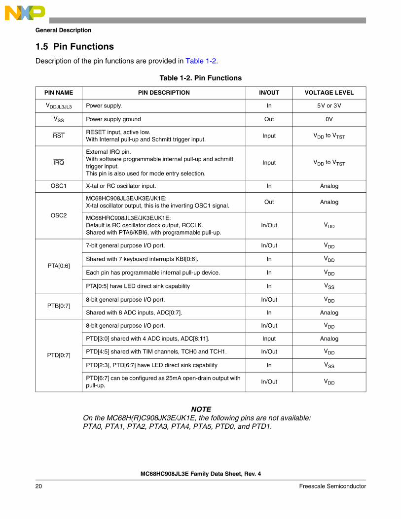
1.5 Pin Functions
Description of the pin functions are provided in Table 1-2.
NOTEOn the MC68H(R)C908JK3E/JK1E, the following pins are not available:PTA0, PTA1, PTA2, PTA3, PTA4, PTA5, PTD0, and PTD1.
Table 1-2. Pin Functions
PIN NAME PIN DESCRIPTION IN/OUT VOLTAGE LEVEL
VDDJL3JL3 Power supply. In 5V or 3V
VSS Power supply ground Out 0V
RSTRESET input, active low.With Internal pull-up and Schmitt trigger input.
Input VDD to VTST
IRQ
External IRQ pin.With software programmable internal pull-up and schmitt trigger input.This pin is also used for mode entry selection.
Input VDD to VTST
OSC1 X-tal or RC oscillator input. In Analog
OSC2
MC68HC908JL3E/JK3E/JK1E:X-tal oscillator output, this is the inverting OSC1 signal.
Out Analog
MC68HRC908JL3E/JK3E/JK1E:Default is RC oscillator clock output, RCCLK.Shared with PTA6/KBI6, with programmable pull-up.
In/Out VDD
PTA[0:6]
7-bit general purpose I/O port. In/Out VDD
Shared with 7 keyboard interrupts KBI[0:6]. In VDD
Each pin has programmable internal pull-up device. In VDD
PTA[0:5] have LED direct sink capability In VSS
PTB[0:7]8-bit general purpose I/O port. In/Out VDD
Shared with 8 ADC inputs, ADC[0:7]. In Analog
PTD[0:7]
8-bit general purpose I/O port. In/Out VDD
PTD[3:0] shared with 4 ADC inputs, ADC[8:11]. Input Analog
PTD[4:5] shared with TIM channels, TCH0 and TCH1. In/Out VDD
PTD[2:3], PTD[6:7] have LED direct sink capability In VSS
PTD[6:7] can be configured as 25mA open-drain output with pull-up.
In/Out VDD
MC68HC908JL3E Family Data Sheet, Rev. 4
20 Freescale Semiconductor

Chapter 2 Memory
2.1 Introduction
The CPU08 can address 64 Kbytes of memory space. The memory map, shown in Figure 2-1, includes:• 4,096 bytes of user Flash — MC68H(R)C908JL3E/JK3E
1,536 bytes of user Flash — MC68H(R)C908JK1E• 128 bytes of RAM• 48 bytes of user-defined vectors• 960 bytes of Monitor ROM
2.2 I/O Section
Addresses $0000–$003F, shown in Figure 2-2, contain most of the control, status, and data registers. Additional I/O registers have the following addresses:
• $FE00; Break Status Register, BSR• $FE01; Reset Status Register, RSR• $FE03; Break Flag Control Register, BFCR• $FE04; Interrupt Status Register 1, INT1• $FE05; Interrupt Status Register 2, INT2• $FE06; Interrupt Status Register 3, INT3• $FE08; Flash Control Register, FLCR• $FE09; Flash Block Protect Register, FLBPR• $FE0C; Break Address Register High, BRKH• $FE0D; Break Address Register Low, BRKL• $FE0E; Break Status and Control Register, BRKSCR• $FFFF; COP Control Register, COPCTL
2.3 Monitor ROM
The 960 bytes at addresses $FC00–$FDFF and $FE10–$FFCF are reserved ROM addresses that contain the instructions for the monitor functions. (See Chapter 7 Monitor ROM (MON).)
MC68HC908JL3E Family Data Sheet, Rev. 4
Freescale Semiconductor 21

Memory
$0000↓
$003F
I/O REGISTERS64 BYTES
$0040↓
$007F
RESERVED64 BYTES
$0080↓
$00FF
RAM128 BYTES
$0100↓
$EBFF
UNIMPLEMENTED60,160 BYTES UNIMPLEMENTED
62,720 BYTES
$0100↓
$F5FF
$EC00↓
$FBFF
FLASH MEMORYMC68H(R)C908JL3E/JK3E
4,096 BYTESFLASH MEMORY
MC68H(R)C908JK1E1,536 BYTES
$F600↓
$FBFF
$FC00↓
$FDFF
MONITOR ROM512 BYTES
$FE00 BREAK STATUS REGISTER (BSR)
$FE01 RESET STATUS REGISTER (RSR)
$FE02 RESERVED (UBAR)
$FE03 BREAK FLAG CONTROL REGISTER (BFCR)
$FE04 INTERRUPT STATUS REGISTER 1 (INT1)
$FE05 INTERRUPT STATUS REGISTER 2 (INT2)
$FE06 INTERRUPT STATUS REGISTER 3 (INT3)
$FE07 RESERVED
$FE08 FLASH CONTROL REGISTER (FLCR)
$FE09 FLASH BLOCK PROTECT REGISTER (FLBPR)
$FE0A RESERVED
$FE0B RESERVED
$FE0C BREAK ADDRESS HIGH REGISTER (BRKH)
$FE0D BREAK ADDRESS LOW REGISTER (BRKL)
$FE0E BREAK STATUS AND CONTROL REGISTER (BRKSCR)
$FE0F RESERVED
$FE10↓
$FFCF
MONITOR ROM448 BYTES
$FFD0↓
$FFFF
USER VECTORS48 BYTES
Figure 2-1. Memory Map
MC68HC908JL3E Family Data Sheet, Rev. 4
22 Freescale Semiconductor

Monitor ROM
Addr. Register Name Bit 7 6 5 4 3 2 1 Bit 0
$0000Port A Data Register
(PTA)
Read: 0PTA6 PTA5 PTA4 PTA3 PTA2 PTA1 PTA0
Write:
Reset: Unaffected by reset
$0001Port B Data Register
(PTB)
Read:PTB7 PTB6 PTB5 PTB4 PTB3 PTB2 PTB1 PTB0
Write:
Reset: Unaffected by reset
$0002 Unimplemented
Read:
Write:
$0003Port D Data Register
(PTD)
Read:PTD7 PTD6 PTD5 PTD4 PTD3 PTD2 PTD1 PTD0
Write:
Reset: Unaffected by reset
$0004Data Direction Register A
(DDRA)
Read: 0DDRA6 DDRA5 DDRA4 DDRA3 DDRA2 DDRA1 DDRA0
Write:
Reset: 0 0 0 0 0 0 0 0
$0005Data Direction Register B
(DDRB)
Read:DDRB7 DDRB6 DDRB5 DDRB4 DDRB3 DDRB2 DDRB1 DDRB0
Write:
Reset: 0 0 0 0 0 0 0 0
$0006 Unimplemented
Read:
Write:
$0007Data Direction Register D
(DDRD)
Read:DDRD7 DDRD6 DDRD5 DDRD4 DDRD3 DDRD2 DDRD1 DDRD0
Write:
Reset: 0 0 0 0 0 0 0 0
$0008↓
$0009 Unimplemented
Read:
Write:
$000APort D Control Register
(PDCR)
Read: 0 0 0 0SLOWD7 SLOWD6 PTDPU7 PTDPU6
Write:
Reset: 0 0 0 0 0 0 0 0
$000B↓
$000CUnimplemented
Read:
Write:
$000DPort A Input Pull-up Enable
Register (PTAPUE)
Read:PTA6EN PTAPUE6 PTAPUE5 PTAPUE4 PTAPUE3 PTAPUE2 PTAPUE1 PTAPUE0
Write:
Reset: 0 0 0 0 0 0 0 0
$000E↓
$0019Unimplemented
Read:
Write:
= Unimplemented R = Reserved
Figure 2-2. Control, Status, and Data Registers (Sheet 1 of 4)
MC68HC908JL3E Family Data Sheet, Rev. 4
Freescale Semiconductor 23

Memory
$001AKeyboard Status and Control
Register (KBSCR)
Read: 0 0 0 0 KEYF 0IMASKK MODEK
Write: ACKK
Reset: 0 0 0 0 0 0 0 0
$001BKeyboard Interrupt Enable
Register (KBIER)
Read: 0KBIE6 KBIE5 KBIE4 KBIE3 KBIE2 KBIE1 KBIE0
Write:
Reset: 0 0 0 0 0 0 0 0
$001CUnimplemented
Read:
Write:
$001DIRQ Status and Control
Register(INTSCR)
Read: 0 0 0 0 IRQF 0IMASK MODE
Write: ACK
Reset: 0 0 0 0 0 0 0 0
$001EConfiguration Register 2
(CONFIG2)†
Read:IRQPUD R R LVIT1 LVIT0 R R R
Write:
Reset: 0 0 0 0* 0* 0 0 0
$001FConfiguration Register 1
(CONFIG1)†
Read:COPRS R R LVID R SSREC STOP COPD
Write:
Reset: 0 0 0 0 0 0 0 0
† One-time writable register after each reset. * LVIT1 and LVIT0 reset to 0 by a power-on reset (POR) only.
$0020TIM Status and Control
Register (TSC)
Read: TOFTOIE TSTOP
0 0PS2 PS1 PS0
Write: 0 TRST
Reset: 0 0 1 0 0 0 0 0
$0021TIM Counter Register High
(TCNTH)
Read: Bit15 Bit14 Bit13 Bit12 Bit11 Bit10 Bit9 Bit8
Write:
Reset: 0 0 0 0 0 0 0 0
$0022TIM Counter Register
Low (TCNTL)
Read: Bit7 Bit6 Bit5 Bit4 Bit3 Bit2 Bit1 Bit0
Write:
Reset: 0 0 0 0 0 0 0 0
$0023TIM Counter Modulo Register
High (TMODH)
Read:Bit15 Bit14 Bit13 Bit12 Bit11 Bit10 Bit9 Bit8
Write:
Reset: 1 1 1 1 1 1 1 1
$0024TIM Counter Modulo Register
Low (TMODL)
Read:Bit7 Bit6 Bit5 Bit4 Bit3 Bit2 Bit1 Bit0
Write:
Reset: 1 1 1 1 1 1 1 1
$0025TIM Channel 0 Status and
Control Register (TSC0)
Read: CH0FCH0IE MS0B MS0A ELS0B ELS0A TOV0 CH0MAX
Write: 0
Reset: 0 0 0 0 0 0 0 0
$0026TIM Channel 0 Register High
(TCH0H)
Read:Bit15 Bit14 Bit13 Bit12 Bit11 Bit10 Bit9 Bit8
Write:
Reset: Indeterminate after reset
Addr. Register Name Bit 7 6 5 4 3 2 1 Bit 0
= Unimplemented R = Reserved
Figure 2-2. Control, Status, and Data Registers (Sheet 2 of 4)
MC68HC908JL3E Family Data Sheet, Rev. 4
24 Freescale Semiconductor

Monitor ROM
$0027TIM Channel 0 Register Low
(TCH0L)
Read:Bit7 Bit6 Bit5 Bit4 Bit3 Bit2 Bit1 Bit0
Write:
Reset: Indeterminate after reset
$0028TIM Channel 1 Status and
Control Register (TSC1)
Read: CH1FCH1IE
0MS1A ELS1B ELS1A TOV1 CH1MAX
Write: 0
Reset: 0 0 0 0 0 0 0 0
$0029TIM Channel 1 Register High
(TCH1H)
Read:Bit15 Bit14 Bit13 Bit12 Bit11 Bit10 Bit9 Bit8
Write:
Reset: Indeterminate after reset
$002ATIM Channel 1 Register Low
(TCH1L)
Read:Bit7 Bit6 Bit5 Bit4 Bit3 Bit2 Bit1 Bit0
Write:
Reset: Indeterminate after reset
$002B↓
$003BUnimplemented
Read:
Write:
$003CADC Status and Control
Register (ADSCR)
Read: COCOAIEN ADCO ADCH4 ADCH3 ADCH2 ADCH1 ADCH0
Write:
Reset: 0 0 0 1 1 1 1 1
$003DADC Data Register
(ADR)
Read: AD7 AD6 AD5 AD4 AD3 AD2 AD1 AD0
Write:
Reset: Indeterminate after reset
$003EADC Input Clock Register
(ADICLK)
Read:ADIV2 ADIV1 ADIV0
0 0 0 0 0
Write:
Reset: 0 0 0 0 0 0 0 0
$003FUnimplemented
Read:
Write:
$FE00Break Status Register
(BSR)
Read:R R R R R R
SBSWR
Write: See note
Reset: 0
Note: Writing a 0 clears SBSW.
$FE01Reset Status Register
(RSR)
Read: POR PIN COP ILOP ILAD MODRST LVI 0
Write:
POR: 1 0 0 0 0 0 0 0
$FE02 Reserved
Read:R R R R R R R R
Write:
$FE03Break Flag Control
Register (BFCR)
Read:BCFE R R R R R R R
Write:
Reset: 0
Addr. Register Name Bit 7 6 5 4 3 2 1 Bit 0
= Unimplemented R = Reserved
Figure 2-2. Control, Status, and Data Registers (Sheet 3 of 4)
MC68HC908JL3E Family Data Sheet, Rev. 4
Freescale Semiconductor 25

Memory
$FE04Interrupt Status Register 1
(INT1)
Read: 0 IF5 IF4 IF3 0 IF1 0 0
Write: R R R R R R R R
Reset: 0 0 0 0 0 0 0 0
$FE05Interrupt Status Register 2
(INT2)
Read: IF14 0 0 0 0 0 0 0
Write: R R R R R R R R
Reset: 0 0 0 0 0 0 0 0
$FE06Interrupt Status Register 3
(INT3)
Read: 0 0 0 0 0 0 0 IF15
Write: R R R R R R R R
Reset: 0 0 0 0 0 0 0 0
$FE07 Reserved
Read:R R R R R R R R
Write:
$FE08Flash Control Register
(FLCR)
Read: 0 0 0 0HVEN MASS ERASE PGM
Write:
Reset: 0 0 0 0 0 0 0 0
$FE09Flash Block Protect Register (FLBPR)
Read:BPR7 BPR6 BPR5 BPR4 BPR3 BPR2 BPR1 BPR0
Write:
Reset: 0 0 0 0 0 0 0 0
$FE0A↓
$FE0BReserved
Read:R R R R R R R R
Write:
$FE0CBreak Address High
Register (BRKH)
Read:Bit15 Bit14 Bit13 Bit12 Bit11 Bit10 Bit9 Bit8
Write:
Reset: 0 0 0 0 0 0 0 0
$FE0DBreak Address Low
Register (BRKL)
Read:Bit7 Bit6 Bit5 Bit4 Bit3 Bit2 Bit1 Bit0
Write:
Reset: 0 0 0 0 0 0 0 0
$FE0EBreak Status and Control
Register (BRKSCR)
Read:BRKE BRKA
0 0 0 0 0 0
Write:
Reset: 0 0 0 0 0 0 0 0
$FFFFCOP Control Register
(COPCTL)
Read: Low byte of reset vector
Write: Writing clears COP counter (any value)
Reset: Unaffected by reset
Addr. Register Name Bit 7 6 5 4 3 2 1 Bit 0
= Unimplemented R = Reserved
Figure 2-2. Control, Status, and Data Registers (Sheet 4 of 4)
MC68HC908JL3E Family Data Sheet, Rev. 4
26 Freescale Semiconductor

Random-Access Memory (RAM)
2.4 Random-Access Memory (RAM)
Addresses $0080 through $00FF are RAM locations. The location of the stack RAM is programmable. The 16-bit stack pointer allows the stack to be anywhere in the 64-Kbyte memory space.
NOTEFor correct operation, the stack pointer must point only to RAM locations.
Within page zero are 128 bytes of RAM. Because the location of the stack RAM is programmable, all page zero RAM locations can be used for I/O control and user data or code. When the stack pointer is moved from its reset location at $00FF, direct addressing mode instructions can access efficiently all page zero RAM locations. Page zero RAM, therefore, provides ideal locations for frequently accessed global variables.
Before processing an interrupt, the CPU uses five bytes of the stack to save the contents of the CPU registers.
NOTEFor M6805 compatibility, the H register is not stacked.
Table 2-1. Vector Addresses
Vector Priority INT Flag Address Vector
Lowest
Highest
—$FFD0
↓$FFDD
Not Used
IF15$FFDE ADC Conversion Complete Vector (High)
$FFDF ADC Conversion Complete Vector (Low)
IF14$FFE0 Keyboard Vector (High)
$FFE1 Keyboard Vector (Low)
IF13↓
IF6— Not Used
IF5$FFF2 TIM Overflow Vector (High)
$FFF3 TIM Overflow Vector (Low)
IF4$FFF4 TIM Channel 1 Vector (High)
$FFF5 TIM Channel 1 Vector (Low)
IF3$FFF6 TIM Channel 0 Vector (High)
$FFF7 TIM Channel 0 Vector (Low)
IF2 — Not Used
IF1$FFFA IRQ Vector (High)
$FFFB IRQ Vector (Low)
—$FFFC SWI Vector (High)
$FFFD SWI Vector (Low)
—$FFFE Reset Vector (High)
$FFFF Reset Vector (Low)
MC68HC908JL3E Family Data Sheet, Rev. 4
Freescale Semiconductor 27

Memory
During a subroutine call, the CPU uses two bytes of the stack to store the return address. The stack pointer decrements during pushes and increments during pulls.
NOTEBe careful when using nested subroutines. The CPU may overwrite data in the RAM during a subroutine or during the interrupt stacking operation.
2.5 Flash Memory
This sub-section describes the operation of the embedded Flash memory. The Flash memory can be read, programmed, and erased from a single external supply. The program and erase operations are enabled through the use of an internal charge pump.
2.6 Functional Description
The Flash memory consists of an array of 4,096 or 1,536 bytes with an additional 48 bytes for user vectors. The minimum size of Flash memory that can be erased is 64 bytes (a page); and the maximum size of Flash memory that can be programmed in a program cycle is 32 bytes (a row). Program and erase operations are facilitated through control bits in the Flash Control Register (FLCR). Details for these operations appear later in this section. The address ranges for the user memory and vectors are:
• $EC00–$FBFF; user memory; 4,096 bytes; MC68H(R)C908JL3E/JK3E$F600–$FBFF; user memory; 1,536 bytes; MC68H(R)C908JK1E
• $FFD0–$FFFF; user interrupt vectors; 48 bytes
NOTEAn erased bit reads as 1 and a programmed bit reads as 0. A security feature prevents viewing of the Flash contents.(1)
DeviceFlash Memory Size
(Bytes)Memory Address Range
MC68H(R)C908JL3E 4,096 $EC00—$FBFF
MC68H(R)C908JK3E 4,096 $EC00—$FBFF
MC68H(R)C908JK1E 1,536 $F600—$FBFF
Addr. Register Name Bit 7 6 5 4 3 2 1 Bit 0
$FE08Flash Control Register
(FLCR)
Read: 0 0 0 0HVEN MASS ERASE PGM
Write:Reset: 0 0 0 0 0 0 0 0
$FE09Flash Block Protect
Register(FLBPR)
Read:BPR7 BPR6 BPR5 BPR4 BPR3 BPR2 BPR1 BPR0
Write:Reset: 0 0 0 0 0 0 0 0
= Unimplemented
Figure 2-3. Flash I/O Register Summary
1. No security feature is absolutely secure. However, Freescale’s strategy is to make reading or copying the Flash difficult for unauthorized users.
MC68HC908JL3E Family Data Sheet, Rev. 4
28 Freescale Semiconductor

Flash Control Register
2.7 Flash Control Register
The Flash Control Register controls Flash program and erase operations.
HVEN — High Voltage Enable BitThis read/write bit enables high voltage from the charge pump to the memory for either program or erase operation. It can only be set if either PGM=1 or ERASE=1 and the proper sequence for program or erase is followed.
1 = High voltage enabled to array and charge pump on0 = High voltage disabled to array and charge pump off
MASS — Mass Erase Control BitThis read/write bit configures the memory for mass erase operation or page erase operation when the ERASE bit is set.
1 = Mass erase operation selected0 = Page erase operation selected
ERASE — Erase Control BitThis read/write bit configures the memory for erase operation. This bit and the PGM bit should not be set to 1 at the same time.
1 = Erase operation selected0 = Erase operation not selected
PGM — Program Control BitThis read/write bit configures the memory for program operation. This bit and the ERASE bit should not be set to 1 at the same time.
1 = Program operation selected0 = Program operation not selected
Address: $FE08
Bit 7 6 5 4 3 2 1 Bit 0
Read: 0 0 0 0HVEN MASS ERASE PGM
Write:
Reset: 0 0 0 0 0 0 0 0
= Unimplemented
Figure 2-4. Flash Control Register (FLCR)
MC68HC908JL3E Family Data Sheet, Rev. 4
Freescale Semiconductor 29

Memory
2.8 Flash Page Erase Operation
Use the following procedure to erase a page of Flash memory. A page consists of 64 consecutive bytes starting from addresses $XX00, $XX40, $XX80 or $XXC0. The 48-byte user interrupt vectors area also forms a page. Any page within the 4K bytes user memory area ($EC00–$FBFF) can be erased alone. The 48-byte user interrupt vectors cannot be erased by the page erase operation because of security reasons. Mass erase is required to erase this page.
1. Set the ERASE bit and clear the MASS bit in the Flash Control Register.2. Write any data to any Flash address within the page address range desired. 3. Wait for a time, tnvs (10μs).4. Set the HVEN bit.5. Wait for a time tErase (1ms).6. Clear the ERASE bit.7. Wait for a time, tnvh (5μs).8. Clear the HVEN bit.9. After time, trcv (1μs), the memory can be accessed in read mode again.
NOTEProgramming and erasing of Flash locations cannot be performed by code being executed from the Flash memory. While these operations must be performed in the order as shown, but other unrelated operations may occur between the steps.
2.9 Flash Mass Erase Operation
Use the following procedure to erase the entire Flash memory:1. Set both the ERASE bit and the MASS bit in the Flash Control Register.2. Write any data to any Flash location within the Flash memory address range.3. Wait for a time, tnvs (10μs).4. Set the HVEN bit.5. Wait for a time tMErase (4ms).6. Clear the ERASE bit.7. Wait for a time, tnvh1 (100μs).8. Clear the HVEN bit.9. After time, trcv (1μs), the memory can be accessed in read mode again.
NOTEProgramming and erasing of Flash locations cannot be performed by code being executed from the Flash memory. While these operations must be performed in the order as shown, but other unrelated operations may occur between the steps.
MC68HC908JL3E Family Data Sheet, Rev. 4
30 Freescale Semiconductor

Flash Program Operation
2.10 Flash Program Operation
Programming of the Flash memory is done on a row basis. A row consists of 32 consecutive bytes starting from addresses $XX00, $XX20, $XX40, $XX60, $XX80, $XXA0, $XXC0 or $XXE0. Use this step-by-step procedure to program a row of Flash memory (Figure 2-5 shows a flowchart of the programming algorithm):
1. Set the PGM bit. This configures the memory for program operation and enables the latching of address and data for programming.
2. Write any data to any Flash location within the address range of the row to be programmed.
3. Wait for a time, tnvs (10μs).
4. Set the HVEN bit.
5. Wait for a time, tpgs (5μs).
6. Write data to the byte being programmed.
7. Wait for time, tPROG (30μs).
8. Repeat step 6 and 7 until all the bytes within the row are programmed.
9. Clear the PGM bit.
10. Wait for time, tnvh (5μs).
11. Clear the HVEN bit.
12. After time, trcv (1μs), the memory can be accessed in read mode again.
This program sequence is repeated throughout the memory until all data is programmed.
NOTEThe time between each Flash address change (step 6 to step 6), or the time between the last Flash addressed programmed to clearing the PGM bit (step 6 to step 10), must not exceed the maximum programming time, tPROG max.
NOTEProgramming and erasing of Flash locations cannot be performed by code being executed from the Flash memory. While these operations must be performed in the order shown, other unrelated operations may occur between the steps.
2.11 Flash Protection
Due to the ability of the on-board charge pump to erase and program the Flash memory in the target application, provision is made to protect blocks of memory from unintentional erase or program operations due to system malfunction. This protection is done by use of a Flash Block Protect Register (FLBPR). The FLBPR determines the range of the Flash memory which is to be protected. The range of the protected area starts from a location defined by FLBPR and ends to the bottom of the Flash memory ($FFFF). When the memory is protected, the HVEN bit cannot be set in either ERASE or PROGRAM operations.
MC68HC908JL3E Family Data Sheet, Rev. 4
Freescale Semiconductor 31

Memory
Figure 2-5. Flash Programming Flowchart
Set HVEN bit
Write any data to any Flash addresswithin the row address range desired
Wait for a time, tnvs
Set PGM bit
Wait for a time, tpgs
Write data to the Flash addressto be programmed
Wait for a time, tPROG
Clear PGM bit
Wait for a time, tnvh
Clear HVEN bit
Wait for a time, trcv
Completedprogramming
this row?
Y
N
End of Programming
The time between each Flash address change (step 6 to step 6), or
must not exceed the maximum programmingtime, tPROG max.
the time between the last Flash address programmedto clearing PGM bit (step 6 to step 9)
NOTE:
1
2
3
4
5
6
7
9
10
11
12
Algorithm for programminga row (32 bytes) of Flash memory
This row program algorithm assumes the row/sto be programmed are initially erased.
MC68HC908JL3E Family Data Sheet, Rev. 4
32 Freescale Semiconductor

Flash Block Protect Register
2.12 Flash Block Protect Register
The Flash Block Protect Register is implemented as an 8-bit I/O register. The value in this register determines the starting address of the protected range within the Flash memory.
BPR[7:0] — Flash Block Protect Register Bit 7 to Bit 0BPR[7:1] represent bits [12:6] of a 16-bit memory address. Bits [15:13] are 1’s and bits [5:0] are 0’s.
BPR0 is used only for BPR[7:0] = $FF, for no block protection.The resultant 16-bit address is used for specifying the start address of the Flash memory for block protection. The Flash is protected from this start address to the end of Flash memory, at $FFFF. With this mechanism, the protect start address can be XX00, XX40, XX80, or XXC0 (at page boundaries — 64 bytes) within the Flash memory.
Examples of protect start address:
Address: $FE09
Bit 7 6 5 4 3 2 1 Bit 0
Read:BPR7 BPR6 BPR5 BPR4 BPR3 BPR2 BPR1 BPR0
Write:
Reset: 0 0 0 0 0 0 0 0
Figure 2-6. Flash Block Protect Register (FLBPR)
16-bit memory address
Start address of Flash block protect 1 1 1 0 0 0 0 0 0
BPR[7:1]
BPR[7:0] Start of Address of Protect Range
$00–$60 The entire Flash memory is protected.
$62 or $63(0110 001x)
$EC40 (1110 1100 0100 0000)
$64 or $65(0110 010x)
$EC80 (1110 1100 1000 0000)
$68 or $69(0110 100x)
$ED00 (1110 1101 0000 0000)
and so on...
$DE or $DF(1101 111x)
$FBC0 (1111 1011 1100 0000)
$FE(1111 1110)
$FFC0 (1111 1111 1100 0000)
$FF The entire Flash memory is not protected.
Note:The end address of the protected range is always $FFFF.
MC68HC908JL3E Family Data Sheet, Rev. 4
Freescale Semiconductor 33

Memory
MC68HC908JL3E Family Data Sheet, Rev. 4
34 Freescale Semiconductor

Chapter 3 Configuration Registers (CONFIG)
3.1 Introduction
This section describes the configuration registers (CONFIG1 and CONFIG2). The configuration registers enables or disables the following options:
• Stop mode recovery time (32 × 2OSCOUT cycles or 4096 × 2OSCOUT cycles)• STOP instruction• Computer operating properly module (COP)• COP reset period (COPRS), 8176 × 2OSCOUT or 262,128 × 2OSCOUT• Enable LVI circuit• Select LVI trip voltage
3.2 Functional Description
The configuration register is used in the initialization of various options. The configuration register can be written once after each reset. All of the configuration register bits are cleared during reset. Since the various options affect the operation of the MCU it is recommended that this register be written immediately after reset. The configuration register is located at $001E and $001F, and may be read at anytime.
NOTEThe CONFIG registers are one-time writable by the user after each reset. Upon a reset, the CONFIG registers default to predetermined settings as shown in Figure 3-1 and Figure 3-2.
3.3 Configuration Register 1 (CONFIG1)
COPRS — COP reset period selection bit1 = COP reset cycle is 8176 × 2OSCOUT0 = COP reset cycle is 262,128 × 2OSCOUT
Address: $001F
Bit 7 6 5 4 3 2 1 Bit 0
Read:COPRS R R LVID R SSREC STOP COPD
Write:
Reset: 0 0 0 0 0 0 0 0
R = Reserved
Figure 3-1. Configuration Register 1 (CONFIG1)
MC68HC908JL3E Family Data Sheet, Rev. 4
Freescale Semiconductor 35

Configuration Registers (CONFIG)
LVID — Low Voltage Inhibit Disable Bit1 = Low Voltage Inhibit disabled0 = Low Voltage Inhibit enabled
SSREC — Short Stop Recovery BitSSREC enables the CPU to exit stop mode with a delay of32 × 2OSCOUT cycles instead of a 4096 × 2OSCOUT cycle delay.
1 = Stop mode recovery after 32 × 2OSCOUT cycles0 = Stop mode recovery after 4096 × 2OSCOUT cycles
NOTEExiting stop mode by pulling reset will result in the long stop recovery.
If using an external crystal, do not set the SSREC bit.
STOP — STOP Instruction EnableSTOP enables the STOP instruction.
1 = STOP instruction enabled0 = STOP instruction treated as illegal opcode
COPD — COP Disable BitCOPD disables the COP module. (See Chapter 13 Computer Operating Properly (COP).)
1 = COP module disabled0 = COP module enabled
3.4 Configuration Register 2 (CONFIG2)
IRQPUD — IRQ Pin Pull-up control bit1 = Internal pull-up is disconnected0 = Internal pull-up is connected between IRQ pin and VDD
LVIT1, LVIT0 — Low Voltage Inhibit trip voltage selection bitsDetail description of the LVI control signals is given in Chapter 14 Low Voltage Inhibit (LVI)
Address: $001E
Bit 7 6 5 4 3 2 1 Bit 0
Read:IRQPUD R R LVIT1 LVIT0 R R R
Write:
Reset: 0 0 0Not
affectedNot
affected0 0 0
POR: 0 0 0 0 0 0 0 0
R = Reserved
Figure 3-2. Configuration Register 2 (CONFIG2)
MC68HC908JL3E Family Data Sheet, Rev. 4
36 Freescale Semiconductor

Chapter 4 Central Processor Unit (CPU)
4.1 Introduction
The M68HC08 CPU (central processor unit) is an enhanced and fully object-code-compatible version of the M68HC05 CPU. The CPU08 Reference Manual (document order number CPU08RM/AD) contains a description of the CPU instruction set, addressing modes, and architecture.
4.2 Features
Features of the CPU include:• Object code fully upward-compatible with M68HC05 Family• 16-bit stack pointer with stack manipulation instructions• 16-bit index register with x-register manipulation instructions• 8-MHz CPU internal bus frequency• 64-Kbyte program/data memory space• 16 addressing modes• Memory-to-memory data moves without using accumulator• Fast 8-bit by 8-bit multiply and 16-bit by 8-bit divide instructions• Enhanced binary-coded decimal (BCD) data handling• Modular architecture with expandable internal bus definition for extension of addressing range
beyond 64 Kbytes• Low-power stop and wait modes
4.3 CPU Registers
Figure 4-1 shows the five CPU registers. CPU registers are not part of the memory map.
MC68HC908JL3E Family Data Sheet, Rev. 4
Freescale Semiconductor 37

Central Processor Unit (CPU)
Figure 4-1. CPU Registers
4.3.1 Accumulator
The accumulator is a general-purpose 8-bit register. The CPU uses the accumulator to hold operands and the results of arithmetic/logic operations.
4.3.2 Index Register
The 16-bit index register allows indexed addressing of a 64-Kbyte memory space. H is the upper byte of the index register, and X is the lower byte. H:X is the concatenated 16-bit index register.
In the indexed addressing modes, the CPU uses the contents of the index register to determine the conditional address of the operand.
The index register can serve also as a temporary data storage location.
Bit 7 6 5 4 3 2 1 Bit 0
Read:
Write:
Reset: Unaffected by reset
Figure 4-2. Accumulator (A)
Bit 15 14 13 12 11 10 9 8 7 6 5 4 3 2 1
Bit0
Read:
Write:
Reset: 0 0 0 0 0 0 0 0 X X X X X X X X
X = Indeterminate
Figure 4-3. Index Register (H:X)
ACCUMULATOR (A)
INDEX REGISTER (H:X)
STACK POINTER (SP)
PROGRAM COUNTER (PC)
CONDITION CODE REGISTER (CCR)
CARRY/BORROW FLAGZERO FLAGNEGATIVE FLAGINTERRUPT MASKHALF-CARRY FLAGTWO’S COMPLEMENT OVERFLOW FLAG
V 1 1 H I N Z C
H X
0
0
0
0
7
15
15
15
7 0
MC68HC908JL3E Family Data Sheet, Rev. 4
38 Freescale Semiconductor
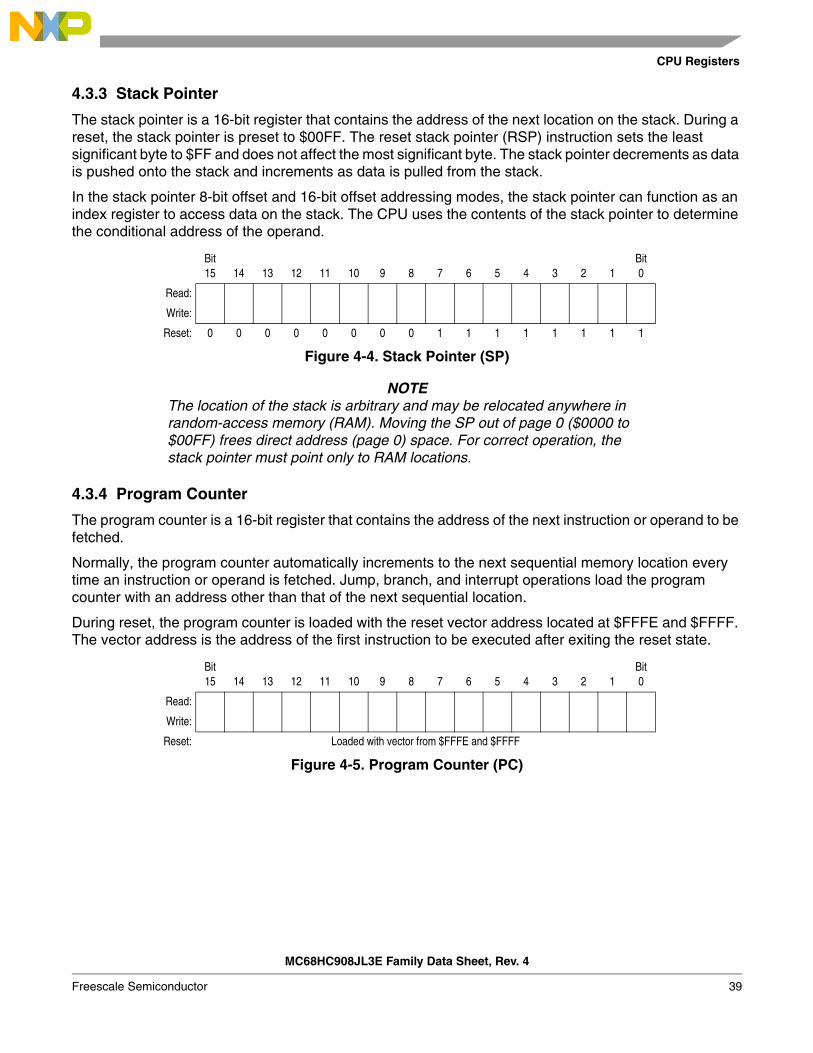
CPU Registers
4.3.3 Stack Pointer
The stack pointer is a 16-bit register that contains the address of the next location on the stack. During a reset, the stack pointer is preset to $00FF. The reset stack pointer (RSP) instruction sets the least significant byte to $FF and does not affect the most significant byte. The stack pointer decrements as data is pushed onto the stack and increments as data is pulled from the stack.
In the stack pointer 8-bit offset and 16-bit offset addressing modes, the stack pointer can function as an index register to access data on the stack. The CPU uses the contents of the stack pointer to determine the conditional address of the operand.
NOTEThe location of the stack is arbitrary and may be relocated anywhere in random-access memory (RAM). Moving the SP out of page 0 ($0000 to $00FF) frees direct address (page 0) space. For correct operation, the stack pointer must point only to RAM locations.
4.3.4 Program Counter
The program counter is a 16-bit register that contains the address of the next instruction or operand to be fetched.
Normally, the program counter automatically increments to the next sequential memory location every time an instruction or operand is fetched. Jump, branch, and interrupt operations load the program counter with an address other than that of the next sequential location.
During reset, the program counter is loaded with the reset vector address located at $FFFE and $FFFF. The vector address is the address of the first instruction to be executed after exiting the reset state.
Bit 15 14 13 12 11 10 9 8 7 6 5 4 3 2 1
Bit0
Read:
Write:
Reset: 0 0 0 0 0 0 0 0 1 1 1 1 1 1 1 1
Figure 4-4. Stack Pointer (SP)
Bit15 14 13 12 11 10 9 8 7 6 5 4 3 2 1
Bit0
Read:
Write:
Reset: Loaded with vector from $FFFE and $FFFF
Figure 4-5. Program Counter (PC)
MC68HC908JL3E Family Data Sheet, Rev. 4
Freescale Semiconductor 39

Central Processor Unit (CPU)
4.3.5 Condition Code Register
The 8-bit condition code register contains the interrupt mask and five flags that indicate the results of the instruction just executed. Bits 6 and 5 are set permanently to 1. The following paragraphs describe the functions of the condition code register.
V — Overflow FlagThe CPU sets the overflow flag when a two's complement overflow occurs. The signed branch instructions BGT, BGE, BLE, and BLT use the overflow flag.
1 = Overflow0 = No overflow
H — Half-Carry FlagThe CPU sets the half-carry flag when a carry occurs between accumulator bits 3 and 4 during an add-without-carry (ADD) or add-with-carry (ADC) operation. The half-carry flag is required for binary-coded decimal (BCD) arithmetic operations. The DAA instruction uses the states of the H and C flags to determine the appropriate correction factor.
1 = Carry between bits 3 and 40 = No carry between bits 3 and 4
I — Interrupt MaskWhen the interrupt mask is set, all maskable CPU interrupts are disabled. CPU interrupts are enabled when the interrupt mask is cleared. When a CPU interrupt occurs, the interrupt mask is set automatically after the CPU registers are saved on the stack, but before the interrupt vector is fetched.
1 = Interrupts disabled0 = Interrupts enabled
NOTETo maintain M6805 Family compatibility, the upper byte of the index register (H) is not stacked automatically. If the interrupt service routine modifies H, then the user must stack and unstack H using the PSHH and PULH instructions.
After the I bit is cleared, the highest-priority interrupt request is serviced first.A return-from-interrupt (RTI) instruction pulls the CPU registers from the stack and restores the interrupt mask from the stack. After any reset, the interrupt mask is set and can be cleared only by the clear interrupt mask software instruction (CLI).
N — Negative FlagThe CPU sets the negative flag when an arithmetic operation, logic operation, or data manipulation produces a negative result, setting bit 7 of the result.
1 = Negative result0 = Non-negative result
Bit 7 6 5 4 3 2 1 Bit 0
Read:V 1 1 H I N Z C
Write:
Reset: X 1 1 X 1 X X X
X = Indeterminate
Figure 4-6. Condition Code Register (CCR)
MC68HC908JL3E Family Data Sheet, Rev. 4
40 Freescale Semiconductor

Arithmetic/Logic Unit (ALU)
Z — Zero FlagThe CPU sets the zero flag when an arithmetic operation, logic operation, or data manipulation produces a result of $00.
1 = Zero result0 = Non-zero result
C — Carry/Borrow FlagThe CPU sets the carry/borrow flag when an addition operation produces a carry out of bit 7 of the accumulator or when a subtraction operation requires a borrow. Some instructions — such as bit test and branch, shift, and rotate — also clear or set the carry/borrow flag.
1 = Carry out of bit 70 = No carry out of bit 7
4.4 Arithmetic/Logic Unit (ALU)
The ALU performs the arithmetic and logic operations defined by the instruction set.
Refer to the CPU08 Reference Manual (document order number CPU08RM/AD) for a description of the instructions and addressing modes and more detail about the architecture of the CPU.
4.5 Low-Power Modes
The WAIT and STOP instructions put the MCU in low power-consumption standby modes.
4.5.1 Wait Mode
The WAIT instruction:• Clears the interrupt mask (I bit) in the condition code register, enabling interrupts. After exit from
wait mode by interrupt, the I bit remains clear. After exit by reset, the I bit is set.• Disables the CPU clock
4.5.2 Stop Mode
The STOP instruction:• Clears the interrupt mask (I bit) in the condition code register, enabling external interrupts. After
exit from stop mode by external interrupt, the I bit remains clear. After exit by reset, the I bit is set.• Disables the CPU clock
After exiting stop mode, the CPU clock begins running after the oscillator stabilization delay.
4.6 CPU During Break Interrupts
If a break module is present on the MCU, the CPU starts a break interrupt by:• Loading the instruction register with the SWI instruction• Loading the program counter with $FFFC:$FFFD or with $FEFC:$FEFD in monitor mode
The break interrupt begins after completion of the CPU instruction in progress. If the break address register match occurs on the last cycle of a CPU instruction, the break interrupt begins immediately.
A return-from-interrupt instruction (RTI) in the break routine ends the break interrupt and returns the MCU to normal operation if the break interrupt has been deasserted.
MC68HC908JL3E Family Data Sheet, Rev. 4
Freescale Semiconductor 41

Central Processor Unit (CPU)
4.7 Instruction Set Summary
Table 4-1 provides a summary of the M68HC08 instruction set.
Table 4-1. Instruction Set Summary (Sheet 1 of 6)
SourceForm Operation Description
Effecton CCR
Ad
dre
ssM
od
e
Op
cod
e
Op
eran
d
Cyc
les
V H I N Z C
ADC #oprADC oprADC oprADC opr,XADC opr,XADC ,XADC opr,SPADC opr,SP
Add with Carry A ← (A) + (M) + (C) –
IMMDIREXTIX2IX1IXSP1SP2
A9B9C9D9E9F9
9EE99ED9
iiddhh llee ffff
ffee ff
23443245
ADD #oprADD oprADD oprADD opr,XADD opr,XADD ,XADD opr,SPADD opr,SP
Add without Carry A ← (A) + (M) –
IMMDIREXTIX2IX1IXSP1SP2
ABBBCBDBEBFB
9EEB9EDB
iiddhh llee ffff
ffee ff
23443245
AIS #opr Add Immediate Value (Signed) to SP SP ← (SP) + (16 « M) – – – – – – IMM A7 ii 2
AIX #opr Add Immediate Value (Signed) to H:X H:X ← (H:X) + (16 « M) – – – – – – IMM AF ii 2
AND #oprAND oprAND oprAND opr,XAND opr,XAND ,XAND opr,SPAND opr,SP
Logical AND A ← (A) & (M) 0 – – –
IMMDIREXTIX2IX1IXSP1SP2
A4B4C4D4E4F4
9EE49ED4
iiddhh llee ffff
ffee ff
23443245
ASL oprASLAASLXASL opr,XASL ,XASL opr,SP
Arithmetic Shift Left(Same as LSL) – –
DIRINHINHIX1IXSP1
3848586878
9E68
dd
ff
ff
411435
ASR oprASRAASRXASR opr,XASR opr,XASR opr,SP
Arithmetic Shift Right – –
DIRINHINHIX1IXSP1
3747576777
9E67
dd
ff
ff
411435
BCC rel Branch if Carry Bit Clear PC ← (PC) + 2 + rel ? (C) = 0 – – – – – – REL 24 rr 3
BCLR n, opr Clear Bit n in M Mn ← 0 – – – – – –
DIR (b0)DIR (b1)DIR (b2)DIR (b3)DIR (b4)DIR (b5)DIR (b6)DIR (b7)
11131517191B1D1F
dd dd dd dd dd dd dd dd
44444444
BCS rel Branch if Carry Bit Set (Same as BLO) PC ← (PC) + 2 + rel ? (C) = 1 – – – – – – REL 25 rr 3
BEQ rel Branch if Equal PC ← (PC) + 2 + rel ? (Z) = 1 – – – – – – REL 27 rr 3
BGE opr Branch if Greater Than or Equal To (Signed Operands) PC ← (PC) + 2 + rel ? (N ⊕ V) = 0 – – – – – – REL 90 rr 3
BGT opr Branch if Greater Than (Signed Operands) PC ← (PC) + 2 + rel ? (Z) | (N ⊕ V) = 0 – – – – – – REL 92 rr 3
BHCC rel Branch if Half Carry Bit Clear PC ← (PC) + 2 + rel ? (H) = 0 – – – – – – REL 28 rr 3
BHCS rel Branch if Half Carry Bit Set PC ← (PC) + 2 + rel ? (H) = 1 – – – – – – REL 29 rr 3
BHI rel Branch if Higher PC ← (PC) + 2 + rel ? (C) | (Z) = 0 – – – – – – REL 22 rr 3
C
b0b7
0
b0b7
C
MC68HC908JL3E Family Data Sheet, Rev. 4
42 Freescale Semiconductor

Instruction Set Summary
BHS rel Branch if Higher or Same(Same as BCC) PC ← (PC) + 2 + rel ? (C) = 0 – – – – – – REL 24 rr 3
BIH rel Branch if IRQ Pin High PC ← (PC) + 2 + rel ? IRQ = 1 – – – – – – REL 2F rr 3
BIL rel Branch if IRQ Pin Low PC ← (PC) + 2 + rel ? IRQ = 0 – – – – – – REL 2E rr 3
BIT #oprBIT oprBIT oprBIT opr,XBIT opr,XBIT ,XBIT opr,SPBIT opr,SP
Bit Test (A) & (M) 0 – – –
IMMDIREXTIX2IX1IXSP1SP2
A5B5C5D5E5F5
9EE59ED5
iiddhh llee ffff
ffee ff
23443245
BLE opr Branch if Less Than or Equal To (Signed Operands) PC ← (PC) + 2 + rel ? (Z) | (N ⊕ V) = 1 – – – – – – REL 93 rr 3
BLO rel Branch if Lower (Same as BCS) PC ← (PC) + 2 + rel ? (C) = 1 – – – – – – REL 25 rr 3
BLS rel Branch if Lower or Same PC ← (PC) + 2 + rel ? (C) | (Z) = 1 – – – – – – REL 23 rr 3
BLT opr Branch if Less Than (Signed Operands) PC ← (PC) + 2 + rel ? (N ⊕ V) =1 – – – – – – REL 91 rr 3
BMC rel Branch if Interrupt Mask Clear PC ← (PC) + 2 + rel ? (I) = 0 – – – – – – REL 2C rr 3
BMI rel Branch if Minus PC ← (PC) + 2 + rel ? (N) = 1 – – – – – – REL 2B rr 3
BMS rel Branch if Interrupt Mask Set PC ← (PC) + 2 + rel ? (I) = 1 – – – – – – REL 2D rr 3
BNE rel Branch if Not Equal PC ← (PC) + 2 + rel ? (Z) = 0 – – – – – – REL 26 rr 3
BPL rel Branch if Plus PC ← (PC) + 2 + rel ? (N) = 0 – – – – – – REL 2A rr 3
BRA rel Branch Always PC ← (PC) + 2 + rel – – – – – – REL 20 rr 3
BRCLR n,opr,rel Branch if Bit n in M Clear PC ← (PC) + 3 + rel ? (Mn) = 0 – – – – –
DIR (b0)DIR (b1)DIR (b2)DIR (b3)DIR (b4)DIR (b5)DIR (b6)DIR (b7)
01030507090B0D0F
dd rrdd rrdd rrdd rrdd rrdd rrdd rrdd rr
55555555
BRN rel Branch Never PC ← (PC) + 2 – – – – – – REL 21 rr 3
BRSET n,opr,rel Branch if Bit n in M Set PC ← (PC) + 3 + rel ? (Mn) = 1 – – – – –
DIR (b0)DIR (b1)DIR (b2)DIR (b3)DIR (b4)DIR (b5)DIR (b6)DIR (b7)
00020406080A0C0E
dd rrdd rrdd rrdd rrdd rrdd rrdd rrdd rr
55555555
BSET n,opr Set Bit n in M Mn ← 1 – – – – – –
DIR (b0)DIR (b1)DIR (b2)DIR (b3)DIR (b4)DIR (b5)DIR (b6)DIR (b7)
10121416181A1C1E
dddddddddddddddd
44444444
BSR rel Branch to Subroutine
PC ← (PC) + 2; push (PCL)SP ← (SP) – 1; push (PCH)
SP ← (SP) – 1PC ← (PC) + rel
– – – – – – REL AD rr 4
CBEQ opr,relCBEQA #opr,relCBEQX #opr,relCBEQ opr,X+,relCBEQ X+,relCBEQ opr,SP,rel
Compare and Branch if Equal
PC ← (PC) + 3 + rel ? (A) – (M) = $00PC ← (PC) + 3 + rel ? (A) – (M) = $00PC ← (PC) + 3 + rel ? (X) – (M) = $00PC ← (PC) + 3 + rel ? (A) – (M) = $00PC ← (PC) + 2 + rel ? (A) – (M) = $00PC ← (PC) + 4 + rel ? (A) – (M) = $00
– – – – – –
DIRIMMIMMIX1+IX+SP1
3141516171
9E61
dd rrii rrii rrff rrrrff rr
544546
CLC Clear Carry Bit C ← 0 – – – – – 0 INH 98 1
CLI Clear Interrupt Mask I ← 0 – – 0 – – – INH 9A 2
Table 4-1. Instruction Set Summary (Sheet 2 of 6)
SourceForm Operation Description
Effecton CCR
Ad
dre
ssM
od
e
Op
cod
e
Op
eran
d
Cyc
les
V H I N Z C
MC68HC908JL3E Family Data Sheet, Rev. 4
Freescale Semiconductor 43

Central Processor Unit (CPU)
CLR oprCLRACLRXCLRHCLR opr,XCLR ,XCLR opr,SP
Clear
M ← $00A ← $00X ← $00H ← $00M ← $00M ← $00M ← $00
0 – – 0 1 –
DIRINHINHINHIX1IXSP1
3F4F5F8C6F7F
9E6F
dd
ff
ff
3111324
CMP #oprCMP oprCMP oprCMP opr,XCMP opr,XCMP ,XCMP opr,SPCMP opr,SP
Compare A with M (A) – (M) – –
IMMDIREXTIX2IX1IXSP1SP2
A1B1C1D1E1F1
9EE19ED1
iiddhh llee ffff
ffee ff
23443245
COM oprCOMACOMXCOM opr,XCOM ,XCOM opr,SP
Complement (One’s Complement)
M ← (M) = $FF – (M)A ← (A) = $FF – (M)X ← (X) = $FF – (M)M ← (M) = $FF – (M)M ← (M) = $FF – (M)M ← (M) = $FF – (M)
0 – – 1
DIRINHINHIX1IXSP1
3343536373
9E63
dd
ff
ff
411435
CPHX #oprCPHX opr Compare H:X with M (H:X) – (M:M + 1) – – IMM
DIR6575
ii ii+1dd
34
CPX #oprCPX oprCPX oprCPX ,XCPX opr,XCPX opr,XCPX opr,SPCPX opr,SP
Compare X with M (X) – (M) – –
IMMDIREXTIX2IX1IXSP1SP2
A3B3C3D3E3F3
9EE39ED3
iiddhh llee ffff
ffee ff
23443245
DAA Decimal Adjust A (A)10 U – – INH 72 2
DBNZ opr,relDBNZA relDBNZX relDBNZ opr,X,relDBNZ X,relDBNZ opr,SP,rel
Decrement and Branch if Not Zero
A ← (A) – 1 or M ← (M) – 1 or X ← (X) – 1PC ← (PC) + 3 + rel ? (result) ≠ 0PC ← (PC) + 2 + rel ? (result) ≠ 0PC ← (PC) + 2 + rel ? (result) ≠ 0PC ← (PC) + 3 + rel ? (result) ≠ 0PC ← (PC) + 2 + rel ? (result) ≠ 0PC ← (PC) + 4 + rel ? (result) ≠ 0
– – – – – –
DIRINHINHIX1IXSP1
3B4B5B6B7B
9E6B
dd rrrrrrff rrrrff rr
533546
DEC oprDECADECXDEC opr,XDEC ,XDEC opr,SP
Decrement
M ← (M) – 1A ← (A) – 1X ← (X) – 1M ← (M) – 1M ← (M) – 1M ← (M) – 1
– – –
DIRINHINHIX1IXSP1
3A4A5A6A7A
9E6A
dd
ff
ff
411435
DIV Divide A ← (H:A)/(X)H ← Remainder – – – – INH 52 7
EOR #oprEOR oprEOR oprEOR opr,XEOR opr,XEOR ,XEOR opr,SPEOR opr,SP
Exclusive OR M with A A ← (A ⊕ M) 0 – – –
IMMDIREXTIX2IX1IXSP1SP2
A8B8C8D8E8F8
9EE89ED8
iiddhh llee ffff
ffee ff
23443245
INC oprINCAINCXINC opr,XINC ,XINC opr,SP
Increment
M ← (M) + 1A ← (A) + 1X ← (X) + 1M ← (M) + 1M ← (M) + 1M ← (M) + 1
– – –
DIRINHINHIX1IXSP1
3C4C5C6C7C
9E6C
dd
ff
ff
411435
Table 4-1. Instruction Set Summary (Sheet 3 of 6)
SourceForm Operation Description
Effecton CCR
Ad
dre
ssM
od
e
Op
cod
e
Op
eran
d
Cyc
les
V H I N Z C
MC68HC908JL3E Family Data Sheet, Rev. 4
44 Freescale Semiconductor
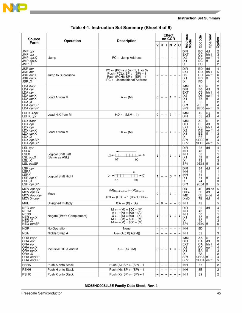
Instruction Set Summary
JMP oprJMP oprJMP opr,XJMP opr,XJMP ,X
Jump PC ← Jump Address – – – – – –
DIREXTIX2IX1IX
BCCCDCECFC
ddhh llee ffff
23432
JSR oprJSR oprJSR opr,XJSR opr,XJSR ,X
Jump to Subroutine
PC ← (PC) + n (n = 1, 2, or 3)Push (PCL); SP ← (SP) – 1Push (PCH); SP ← (SP) – 1PC ← Unconditional Address
– – – – – –
DIREXTIX2IX1IX
BDCDDDEDFD
ddhh llee ffff
45654
LDA #oprLDA oprLDA oprLDA opr,XLDA opr,XLDA ,XLDA opr,SPLDA opr,SP
Load A from M A ← (M) 0 – – –
IMMDIREXTIX2IX1IXSP1SP2
A6B6C6D6E6F6
9EE69ED6
iiddhh llee ffff
ffee ff
23443245
LDHX #oprLDHX opr Load H:X from M H:X ← (M:M + 1) 0 – – – IMM
DIR4555
ii jjdd
34
LDX #oprLDX oprLDX oprLDX opr,XLDX opr,XLDX ,XLDX opr,SPLDX opr,SP
Load X from M X ← (M) 0 – – –
IMMDIREXTIX2IX1IXSP1SP2
AEBECEDEEEFE
9EEE9EDE
iiddhh llee ffff
ffee ff
23443245
LSL oprLSLALSLXLSL opr,XLSL ,XLSL opr,SP
Logical Shift Left(Same as ASL) – –
DIRINHINHIX1IXSP1
3848586878
9E68
dd
ff
ff
411435
LSR oprLSRALSRXLSR opr,XLSR ,XLSR opr,SP
Logical Shift Right – – 0
DIRINHINHIX1IXSP1
3444546474
9E64
dd
ff
ff
411435
MOV opr,oprMOV opr,X+MOV #opr,oprMOV X+,opr
Move(M)Destination ← (M)Source
H:X ← (H:X) + 1 (IX+D, DIX+)0 – – –
DDDIX+IMDIX+D
4E5E6E7E
dd ddddii dddd
5444
MUL Unsigned multiply X:A ← (X) × (A) – 0 – – – 0 INH 42 5
NEG oprNEGANEGXNEG opr,XNEG ,XNEG opr,SP
Negate (Two’s Complement)
M ← –(M) = $00 – (M)A ← –(A) = $00 – (A)X ← –(X) = $00 – (X)M ← –(M) = $00 – (M)M ← –(M) = $00 – (M)
– –
DIRINHINHIX1IXSP1
3040506070
9E60
dd
ff
ff
411435
NOP No Operation None – – – – – – INH 9D 1
NSA Nibble Swap A A ← (A[3:0]:A[7:4]) – – – – – – INH 62 3
ORA #oprORA oprORA oprORA opr,XORA opr,XORA ,XORA opr,SPORA opr,SP
Inclusive OR A and M A ← (A) | (M) 0 – – –
IMMDIREXTIX2IX1IXSP1SP2
AABACADAEAFA
9EEA9EDA
iiddhh llee ffff
ffee ff
23443245
PSHA Push A onto Stack Push (A); SP ← (SP) – 1 – – – – – – INH 87 2
PSHH Push H onto Stack Push (H); SP ← (SP) – 1 – – – – – – INH 8B 2
PSHX Push X onto Stack Push (X); SP ← (SP) – 1 – – – – – – INH 89 2
Table 4-1. Instruction Set Summary (Sheet 4 of 6)
SourceForm Operation Description
Effecton CCR
Ad
dre
ssM
od
e
Op
cod
e
Op
eran
d
Cyc
les
V H I N Z C
C
b0b7
0
b0b7
C0
MC68HC908JL3E Family Data Sheet, Rev. 4
Freescale Semiconductor 45

Central Processor Unit (CPU)
PULA Pull A from Stack SP ← (SP + 1); Pull (A) – – – – – – INH 86 2
PULH Pull H from Stack SP ← (SP + 1); Pull (H) – – – – – – INH 8A 2
PULX Pull X from Stack SP ← (SP + 1); Pull (X) – – – – – – INH 88 2
ROL oprROLAROLXROL opr,XROL ,XROL opr,SP
Rotate Left through Carry – –
DIRINHINHIX1IXSP1
3949596979
9E69
dd
ff
ff
411435
ROR oprRORARORXROR opr,XROR ,XROR opr,SP
Rotate Right through Carry – –
DIRINHINHIX1IXSP1
3646566676
9E66
dd
ff
ff
411435
RSP Reset Stack Pointer SP ← $FF – – – – – – INH 9C 1
RTI Return from Interrupt
SP ← (SP) + 1; Pull (CCR)SP ← (SP) + 1; Pull (A)SP ← (SP) + 1; Pull (X)
SP ← (SP) + 1; Pull (PCH)SP ← (SP) + 1; Pull (PCL)
INH 80 7
RTS Return from Subroutine SP ← SP + 1; Pull (PCH)SP ← SP + 1; Pull (PCL) – – – – – – INH 81 4
SBC #oprSBC oprSBC oprSBC opr,XSBC opr,XSBC ,XSBC opr,SPSBC opr,SP
Subtract with Carry A ← (A) – (M) – (C) – –
IMMDIREXTIX2IX1IXSP1SP2
A2B2C2D2E2F2
9EE29ED2
iiddhh llee ffff
ffee ff
23443245
SEC Set Carry Bit C ← 1 – – – – – 1 INH 99 1
SEI Set Interrupt Mask I ← 1 – – 1 – – – INH 9B 2
STA oprSTA oprSTA opr,XSTA opr,XSTA ,XSTA opr,SPSTA opr,SP
Store A in M M ← (A) 0 – – –
DIREXTIX2IX1IXSP1SP2
B7C7D7E7F7
9EE79ED7
ddhh llee ffff
ffee ff
3443245
STHX opr Store H:X in M (M:M + 1) ← (H:X) 0 – – – DIR 35 dd 4
STOPEnable Interrupts, Stop Processing, Refer to MCU Documentation
I ← 0; Stop Processing – – 0 – – – INH 8E 1
STX oprSTX oprSTX opr,XSTX opr,XSTX ,XSTX opr,SPSTX opr,SP
Store X in M M ← (X) 0 – – –
DIREXTIX2IX1IXSP1SP2
BFCFDFEFFF
9EEF9EDF
ddhh llee ffff
ffee ff
3443245
SUB #oprSUB oprSUB oprSUB opr,XSUB opr,XSUB ,XSUB opr,SPSUB opr,SP
Subtract A ← (A) – (M) – –
IMMDIREXTIX2IX1IXSP1SP2
A0B0C0D0E0F0
9EE09ED0
iiddhh llee ffff
ffee ff
23443245
Table 4-1. Instruction Set Summary (Sheet 5 of 6)
SourceForm Operation Description
Effecton CCR
Ad
dre
ssM
od
e
Op
cod
e
Op
eran
d
Cyc
les
V H I N Z C
C
b0b7
b0b7
C
MC68HC908JL3E Family Data Sheet, Rev. 4
46 Freescale Semiconductor
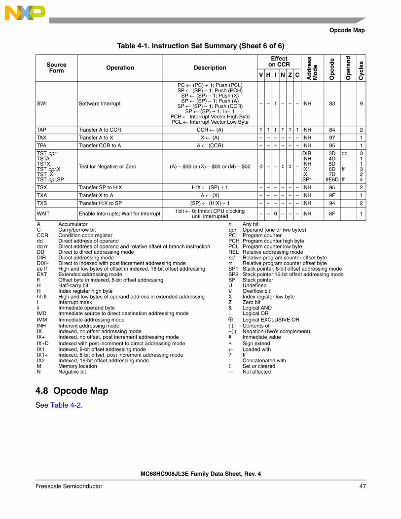
Opcode Map
4.8 Opcode Map
See Table 4-2.
SWI Software Interrupt
PC ← (PC) + 1; Push (PCL)SP ← (SP) – 1; Push (PCH)
SP ← (SP) – 1; Push (X)SP ← (SP) – 1; Push (A)
SP ← (SP) – 1; Push (CCR)SP ← (SP) – 1; I ← 1
PCH ← Interrupt Vector High BytePCL ← Interrupt Vector Low Byte
– – 1 – – – INH 83 9
TAP Transfer A to CCR CCR ← (A) INH 84 2
TAX Transfer A to X X ← (A) – – – – – – INH 97 1
TPA Transfer CCR to A A ← (CCR) – – – – – – INH 85 1
TST oprTSTATSTXTST opr,XTST ,XTST opr,SP
Test for Negative or Zero (A) – $00 or (X) – $00 or (M) – $00 0 – – –
DIRINHINHIX1IXSP1
3D4D5D6D7D
9E6D
dd
ff
ff
311324
TSX Transfer SP to H:X H:X ← (SP) + 1 – – – – – – INH 95 2
TXA Transfer X to A A ← (X) – – – – – – INH 9F 1
TXS Transfer H:X to SP (SP) ← (H:X) – 1 – – – – – – INH 94 2
WAIT Enable Interrupts; Wait for Interrupt I bit ← 0; Inhibit CPU clockinguntil interrupted – – 0 – – – INH 8F 1
A Accumulator n Any bitC Carry/borrow bit opr Operand (one or two bytes)CCR Condition code register PC Program counterdd Direct address of operand PCH Program counter high bytedd rr Direct address of operand and relative offset of branch instruction PCL Program counter low byteDD Direct to direct addressing mode REL Relative addressing modeDIR Direct addressing mode rel Relative program counter offset byteDIX+ Direct to indexed with post increment addressing mode rr Relative program counter offset byteee ff High and low bytes of offset in indexed, 16-bit offset addressing SP1 Stack pointer, 8-bit offset addressing modeEXT Extended addressing mode SP2 Stack pointer 16-bit offset addressing modeff Offset byte in indexed, 8-bit offset addressing SP Stack pointerH Half-carry bit U UndefinedH Index register high byte V Overflow bithh ll High and low bytes of operand address in extended addressing X Index register low byteI Interrupt mask Z Zero bitii Immediate operand byte & Logical ANDIMD Immediate source to direct destination addressing mode | Logical ORIMM Immediate addressing mode ⊕ Logical EXCLUSIVE ORINH Inherent addressing mode ( ) Contents ofIX Indexed, no offset addressing mode –( ) Negation (two’s complement)IX+ Indexed, no offset, post increment addressing mode # Immediate valueIX+D Indexed with post increment to direct addressing mode « Sign extendIX1 Indexed, 8-bit offset addressing mode ← Loaded withIX1+ Indexed, 8-bit offset, post increment addressing mode ? IfIX2 Indexed, 16-bit offset addressing mode : Concatenated withM Memory location Set or clearedN Negative bit — Not affected
Table 4-1. Instruction Set Summary (Sheet 6 of 6)
SourceForm Operation Description
Effecton CCR
Ad
dre
ssM
od
e
Op
cod
e
Op
eran
d
Cyc
les
V H I N Z C
MC68HC908JL3E Family Data Sheet, Rev. 4
Freescale Semiconductor 47

4 Cen
tral Pro
cessor U
nit (C
PU
)
Register/MemoryIX2 SP2 IX1 SP1 IX
D 9ED E 9EE F
4SUB
3 IX2
5SUB
4 SP2
3SUB
2 IX1
4SUB
3 SP1
2SUB
1 IX4
CMP3 IX2
5CMP
4 SP2
3CMP
2 IX1
4CMP
3 SP1
2CMP
1 IX4
SBC3 IX2
5SBC
4 SP2
3SBC
2 IX1
4SBC
3 SP1
2SBC
1 IX4
CPX3 IX2
5CPX
4 SP2
3CPX
2 IX1
4CPX
3 SP1
2CPX
1 IX4
AND3 IX2
5AND
4 SP2
3AND
2 IX1
4AND
3 SP1
2AND
1 IX4
BIT3 IX2
5BIT
4 SP2
3BIT
2 IX1
4BIT
3 SP1
2BIT
1 IX4
LDA3 IX2
5LDA
4 SP2
3LDA
2 IX1
4LDA
3 SP1
2LDA
1 IX4
STA3 IX2
5STA
4 SP2
3STA
2 IX1
4STA
3 SP1
2STA
1 IX4
EOR3 IX2
5EOR
4 SP2
3EOR
2 IX1
4EOR
3 SP1
2EOR
1 IX4
ADC3 IX2
5ADC
4 SP2
3ADC
2 IX1
4ADC
3 SP1
2ADC
1 IX4
ORA3 IX2
5ORA
4 SP2
3ORA
2 IX1
4ORA
3 SP1
2ORA
1 IX4
ADD3 IX2
5ADD
4 SP2
3ADD
2 IX1
4ADD
3 SP1
2ADD
1 IX4
JMP3 IX2
3JMP
2 IX1
2JMP
1 IX6
JSR3 IX2
5JSR
2 IX1
4JSR
1 IX4
LDX3 IX2
5LDX
4 SP2
3LDX
2 IX1
4LDX
3 SP1
2LDX
1 IX4
STX3 IX2
5STX
4 SP2
3STX
2 IX1
4STX
3 SP1
2STX
1 IX
High Byte of Opcode in Hexadecimal
CyclesOpcode MnemonicNumber of Bytes / Addressing Mode
MC
68HC
908JL3E
Family D
ata Sh
eet, Rev. 4
8F
reescale Sem
iconductor
Table 4-2. Opcode MapBit Manipulation Branch Read-Modify-Write Control
DIR DIR REL DIR INH INH IX1 SP1 IX INH INH IMM DIR EXT
0 1 2 3 4 5 6 9E6 7 8 9 A B C
05
BRSET03 DIR
4BSET0
2 DIR
3BRA
2 REL
4NEG
2 DIR
1NEGA
1 INH
1NEGX
1 INH
4NEG
2 IX1
5NEG
3 SP1
3NEG
1 IX
7RTI
1 INH
3BGE
2 REL
2SUB
2 IMM
3SUB
2 DIR
4SUB
3 EXT
15
BRCLR03 DIR
4BCLR0
2 DIR
3BRN
2 REL
5CBEQ
3 DIR
4CBEQA3 IMM
4CBEQX3 IMM
5CBEQ
3 IX1+
6CBEQ
4 SP1
4CBEQ
2 IX+
4RTS
1 INH
3BLT
2 REL
2CMP
2 IMM
3CMP
2 DIR
4CMP
3 EXT
25
BRSET13 DIR
4BSET1
2 DIR
3BHI
2 REL
5MUL
1 INH
7DIV
1 INH
3NSA
1 INH
2DAA
1 INH
3BGT
2 REL
2SBC
2 IMM
3SBC
2 DIR
4SBC
3 EXT
35
BRCLR13 DIR
4BCLR1
2 DIR
3BLS
2 REL
4COM
2 DIR
1COMA
1 INH
1COMX
1 INH
4COM
2 IX1
5COM
3 SP1
3COM
1 IX
9SWI
1 INH
3BLE
2 REL
2CPX
2 IMM
3CPX
2 DIR
4CPX
3 EXT
45
BRSET23 DIR
4BSET2
2 DIR
3BCC
2 REL
4LSR
2 DIR
1LSRA
1 INH
1LSRX
1 INH
4LSR
2 IX1
5LSR
3 SP1
3LSR
1 IX
2TAP
1 INH
2TXS
1 INH
2AND
2 IMM
3AND
2 DIR
4AND
3 EXT
55
BRCLR23 DIR
4BCLR2
2 DIR
3BCS
2 REL
4STHX
2 DIR
3LDHX
3 IMM
4LDHX
2 DIR
3CPHX
3 IMM
4CPHX
2 DIR
1TPA
1 INH
2TSX
1 INH
2BIT
2 IMM
3BIT
2 DIR
4BIT
3 EXT
65
BRSET33 DIR
4BSET3
2 DIR
3BNE
2 REL
4ROR
2 DIR
1RORA
1 INH
1RORX
1 INH
4ROR
2 IX1
5ROR
3 SP1
3ROR
1 IX
2PULA
1 INH
2LDA
2 IMM
3LDA
2 DIR
4LDA
3 EXT
75
BRCLR33 DIR
4BCLR3
2 DIR
3BEQ
2 REL
4ASR
2 DIR
1ASRA
1 INH
1ASRX
1 INH
4ASR
2 IX1
5ASR
3 SP1
3ASR
1 IX
2PSHA
1 INH
1TAX
1 INH
2AIS
2 IMM
3STA
2 DIR
4STA
3 EXT
85
BRSET43 DIR
4BSET4
2 DIR
3BHCC
2 REL
4LSL
2 DIR
1LSLA
1 INH
1LSLX
1 INH
4LSL
2 IX1
5LSL
3 SP1
3LSL
1 IX
2PULX
1 INH
1CLC
1 INH
2EOR
2 IMM
3EOR
2 DIR
4EOR
3 EXT
95
BRCLR43 DIR
4BCLR4
2 DIR
3BHCS
2 REL
4ROL
2 DIR
1ROLA
1 INH
1ROLX
1 INH
4ROL
2 IX1
5ROL
3 SP1
3ROL
1 IX
2PSHX
1 INH
1SEC
1 INH
2ADC
2 IMM
3ADC
2 DIR
4ADC
3 EXT
A5
BRSET53 DIR
4BSET5
2 DIR
3BPL
2 REL
4DEC
2 DIR
1DECA
1 INH
1DECX
1 INH
4DEC
2 IX1
5DEC
3 SP1
3DEC
1 IX
2PULH
1 INH
2CLI
1 INH
2ORA
2 IMM
3ORA
2 DIR
4ORA
3 EXT
B5
BRCLR53 DIR
4BCLR5
2 DIR
3BMI
2 REL
5DBNZ
3 DIR
3DBNZA2 INH
3DBNZX2 INH
5DBNZ
3 IX1
6DBNZ
4 SP1
4DBNZ
2 IX
2PSHH
1 INH
2SEI
1 INH
2ADD
2 IMM
3ADD
2 DIR
4ADD
3 EXT
C5
BRSET63 DIR
4BSET6
2 DIR
3BMC
2 REL
4INC
2 DIR
1INCA
1 INH
1INCX
1 INH
4INC
2 IX1
5INC
3 SP1
3INC
1 IX
1CLRH
1 INH
1RSP
1 INH
2JMP
2 DIR
3JMP
3 EXT
D5
BRCLR63 DIR
4BCLR6
2 DIR
3BMS
2 REL
3TST
2 DIR
1TSTA
1 INH
1TSTX
1 INH
3TST
2 IX1
4TST
3 SP1
2TST
1 IX
1NOP
1 INH
4BSR
2 REL
4JSR
2 DIR
5JSR
3 EXT
E5
BRSET73 DIR
4BSET7
2 DIR
3BIL
2 REL
5MOV
3 DD
4MOV
2 DIX+
4MOV
3 IMD
4MOV
2 IX+D
1STOP
1 INH *2
LDX2 IMM
3LDX
2 DIR
4LDX
3 EXT
F5
BRCLR73 DIR
4BCLR7
2 DIR
3BIH
2 REL
3CLR
2 DIR
1CLRA
1 INH
1CLRX
1 INH
3CLR
2 IX1
4CLR
3 SP1
2CLR
1 IX
1WAIT
1 INH
1TXA
1 INH
2AIX
2 IMM
3STX
2 DIR
4STX
3 EXT
INH Inherent REL Relative SP1 Stack Pointer, 8-Bit OffsetIMM Immediate IX Indexed, No Offset SP2 Stack Pointer, 16-Bit OffsetDIR Direct IX1 Indexed, 8-Bit Offset IX+ Indexed, No Offset with EXT Extended IX2 Indexed, 16-Bit Offset Post IncrementDD Direct-Direct IMD Immediate-Direct IX1+ Indexed, 1-Byte Offset with IX+D Indexed-Direct DIX+ Direct-Indexed Post Increment*Pre-byte for stack pointer indexed instructions
0
Low Byte of Opcode in Hexadecimal 05
BRSET03 DIR
MSB
LSB
MSB
LSB
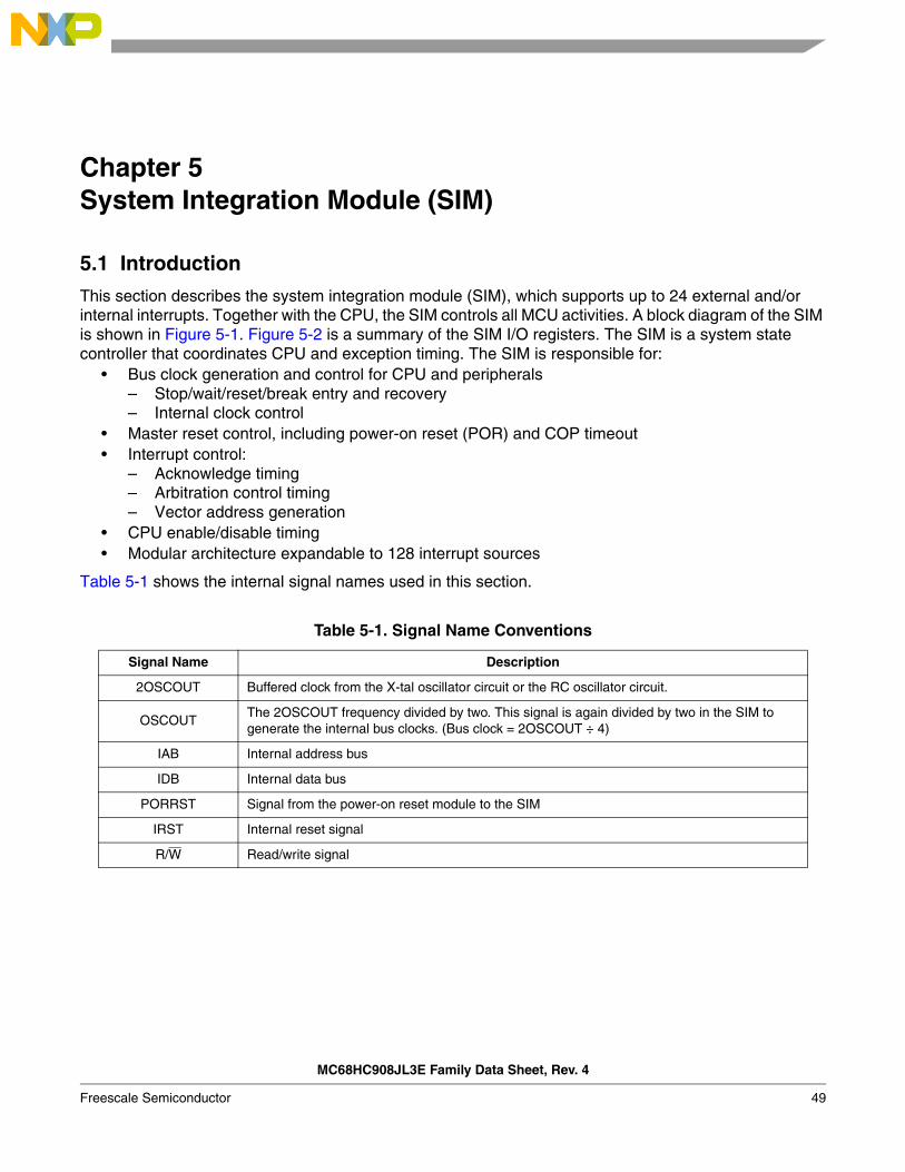
Chapter 5 System Integration Module (SIM)
5.1 Introduction
This section describes the system integration module (SIM), which supports up to 24 external and/or internal interrupts. Together with the CPU, the SIM controls all MCU activities. A block diagram of the SIM is shown in Figure 5-1. Figure 5-2 is a summary of the SIM I/O registers. The SIM is a system state controller that coordinates CPU and exception timing. The SIM is responsible for:
• Bus clock generation and control for CPU and peripherals– Stop/wait/reset/break entry and recovery– Internal clock control
• Master reset control, including power-on reset (POR) and COP timeout• Interrupt control:
– Acknowledge timing– Arbitration control timing – Vector address generation
• CPU enable/disable timing• Modular architecture expandable to 128 interrupt sources
Table 5-1 shows the internal signal names used in this section.
Table 5-1. Signal Name Conventions
Signal Name Description
2OSCOUT Buffered clock from the X-tal oscillator circuit or the RC oscillator circuit.
OSCOUTThe 2OSCOUT frequency divided by two. This signal is again divided by two in the SIM to generate the internal bus clocks. (Bus clock = 2OSCOUT ÷ 4)
IAB Internal address bus
IDB Internal data bus
PORRST Signal from the power-on reset module to the SIM
IRST Internal reset signal
R/W Read/write signal
MC68HC908JL3E Family Data Sheet, Rev. 4
Freescale Semiconductor 49

System Integration Module (SIM)
Figure 5-1. SIM Block Diagram
Addr. Register Name Bit 7 6 5 4 3 2 1 Bit 0
$FE00Break Status Register
(BSR)
Read:R R R R R R
SBSWR
Write: NOTEReset: 0 0 0 0 0 0 0 0
Note: Writing a 0 clears SBSW.
$FE01Reset Status Register
(RSR)
Read: POR PIN COP ILOP ILAD MODRST LVI 0Write:POR: 1 0 0 0 0 0 0 0
$FE02 ReservedRead:
R R R R R R R RWrite:Reset:
$FE03Break Flag Control
Register (BFCR)
Read:BCFE R R R R R R R
Write:Reset: 0
= Unimplemented R = Reserved
Figure 5-2. SIM I/O Register Summary
STOP/WAIT
CLOCKCONTROL CLOCK GENERATORS
POR CONTROL
RESET PIN CONTROL
SIM RESET STATUS REGISTER
INTERRUPT CONTROLAND PRIORITY DECODE
MODULE STOP
MODULE WAIT
CPU STOP (FROM CPU)CPU WAIT (FROM CPU)
SIMOSCEN (TO OSCILLATOR)
OSCOUT (FROM OSCILLATOR)
INTERNAL CLOCKS
MASTERRESET
CONTROL
RESETPIN LOGIC
ILLEGAL OPCODE (FROM CPU)ILLEGAL ADDRESS (FROM ADDRESSMAP DECODERS)COP TIMEOUT (FROM COP MODULE)
INTERRUPT SOURCES
CPU INTERFACE
RESET
CONTROL
SIMCOUNTER COP CLOCK
2OSCOUT (FROM OSCILLATOR)
÷2
USB RESET (FROM USB MODULE)
VDD
INTERNALPULL-UP
MC68HC908JL3E Family Data Sheet, Rev. 4
50 Freescale Semiconductor

SIM Bus Clock Control and Generation
5.2 SIM Bus Clock Control and Generation
The bus clock generator provides system clock signals for the CPU and peripherals on the MCU. The system clocks are generated from an incoming clock, OSCOUT, as shown in Figure 5-3.
Figure 5-3. SIM Clock Signals
5.2.1 Bus Timing
In user mode, the internal bus frequency is the oscillator frequency (2OSCOUT) divided by four.
5.2.2 Clock Start-Up from POR
When the power-on reset module generates a reset, the clocks to the CPU and peripherals are inactive and held in an inactive phase until after the 4096 2OSCOUT cycle POR time-out has completed. The RST pin is driven low by the SIM during this entire period. The IBUS clocks start upon completion of the time-out.
5.2.3 Clocks in Stop Mode and Wait Mode
Upon exit from stop mode by an interrupt, break, or reset, the SIM allows 2OSCOUT to clock the SIM counter. The CPU and peripheral clocks do not become active until after the stop delay time-out. This time-out is selectable as 4096 or 32 2OSCOUT cycles. (See 5.6.2 Stop Mode.)
In wait mode, the CPU clocks are inactive. The SIM also produces two sets of clocks for other modules. Refer to the wait mode subsection of each module to see if the module is active or inactive in wait mode. Some modules can be programmed to be active in wait mode.
$FE04Interrupt Status Register 1
(INT1)
Read: 0 IF5 IF4 IF3 0 IF1 0 0Write: R R R R R R R RReset: 0 0 0 0 0 0 0 0
$FE05Interrupt Status Register 2
(INT2)
Read: IF14 0 0 0 0 0 0 0Write: R R R R R R R RReset: 0 0 0 0 0 0 0 0
$FE06Interrupt Status Register 3
(INT3)
Read: 0 0 0 0 0 0 0 IF15Write: R R R R R R R RReset: 0 0 0 0 0 0 0 0
Addr. Register Name Bit 7 6 5 4 3 2 1 Bit 0
= Unimplemented R = Reserved
Figure 5-2. SIM I/O Register Summary
÷ 2 BUS CLOCKGENERATORS
SIM
SIM COUNTERFROM
OSCILLATOR
FROMOSCILLATOR
OSCOUT
2OSCOUT
MC68HC908JL3E Family Data Sheet, Rev. 4
Freescale Semiconductor 51

System Integration Module (SIM)
5.3 Reset and System Initialization
The MCU has these reset sources:
• Power-on reset module (POR)
• External reset pin (RST)
• Computer operating properly module (COP)
• Low-voltage inhibit module (LVI)
• Illegal opcode
• Illegal address
All of these resets produce the vector $FFFE–$FFFF ($FEFE–$FEFF in Monitor mode) and assert the internal reset signal (IRST). IRST causes all registers to be returned to their default values and all modules to be returned to their reset states.
An internal reset clears the SIM counter (see 5.4 SIM Counter), but an external reset does not. Each of the resets sets a corresponding bit in the reset status register (RSR). (See 5.7 SIM Registers.)
5.3.1 External Pin Reset
The RST pin circuits include an internal pull-up device. Pulling the asynchronous RST pin low halts all processing. The PIN bit of the reset status register (RSR) is set as long as RST is held low for a minimum of 67 2OSCOUT cycles, assuming that the POR was not the source of the reset. See Table 5-2 for details. Figure 5-4 shows the relative timing.
Figure 5-4. External Reset Timing
5.3.2 Active Resets from Internal Sources
All internal reset sources actively pull the RST pin low for 32 2OSCOUT cycles to allow resetting of external peripherals. The internal reset signal IRST continues to be asserted for an additional 32 cycles (Figure 5-5). An internal reset can be caused by an illegal address, illegal opcode, COP time-out, or POR. (See Figure 5-6.) Note that for POR resets, the SIM cycles through 4096 2OSCOUT cycles during which the SIM forces the RST pin low. The internal reset signal then follows the sequence from the falling edge of RST shown in Figure 5-5.
Table 5-2. PIN Bit Set Timing
Reset Type Number of Cycles Required to Set PIN
POR 4163 (4096 + 64 + 3)
All others 67 (64 + 3)
RST
IAB PC VECT H VECT L
2OSCOUT
MC68HC908JL3E Family Data Sheet, Rev. 4
52 Freescale Semiconductor
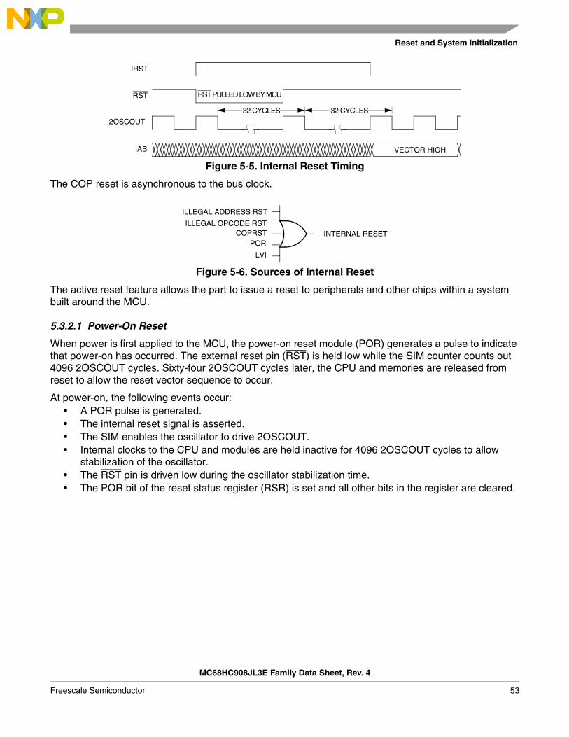
Reset and System Initialization
Figure 5-5. Internal Reset Timing
The COP reset is asynchronous to the bus clock.
Figure 5-6. Sources of Internal Reset
The active reset feature allows the part to issue a reset to peripherals and other chips within a system built around the MCU.
5.3.2.1 Power-On Reset
When power is first applied to the MCU, the power-on reset module (POR) generates a pulse to indicate that power-on has occurred. The external reset pin (RST) is held low while the SIM counter counts out 4096 2OSCOUT cycles. Sixty-four 2OSCOUT cycles later, the CPU and memories are released from reset to allow the reset vector sequence to occur.
At power-on, the following events occur:• A POR pulse is generated.• The internal reset signal is asserted.• The SIM enables the oscillator to drive 2OSCOUT.• Internal clocks to the CPU and modules are held inactive for 4096 2OSCOUT cycles to allow
stabilization of the oscillator.• The RST pin is driven low during the oscillator stabilization time.• The POR bit of the reset status register (RSR) is set and all other bits in the register are cleared.
IRST
RST RST PULLED LOW BY MCU
IAB
32 CYCLES 32 CYCLES
VECTOR HIGH
2OSCOUT
ILLEGAL ADDRESS RST
ILLEGAL OPCODE RSTCOPRST
POR
LVI
INTERNAL RESET
MC68HC908JL3E Family Data Sheet, Rev. 4
Freescale Semiconductor 53

System Integration Module (SIM)
Figure 5-7. POR Recovery
5.3.2.2 Computer Operating Properly (COP) Reset
An input to the SIM is reserved for the COP reset signal. The overflow of the COP counter causes an internal reset and sets the COP bit in the reset status register (RSR). The SIM actively pulls down the RST pin for all internal reset sources.
To prevent a COP module time-out, write any value to location $FFFF. Writing to location $FFFF clears the COP counter and stages 12 through 5 of the SIM counter. The SIM counter output, which occurs at least every 4080 2OSCOUT cycles, drives the COP counter. The COP should be serviced as soon as possible out of reset to guarantee the maximum amount of time before the first time-out.
The COP module is disabled if the RST pin or the IRQ pin is held at VTST while the MCU is in monitor mode. The COP module can be disabled only through combinational logic conditioned with the high voltage signal on the RST or the IRQ pin. This prevents the COP from becoming disabled as a result of external noise. During a break state, VTST on the RST pin disables the COP module.
5.3.2.3 Illegal Opcode Reset
The SIM decodes signals from the CPU to detect illegal instructions. An illegal instruction sets the ILOP bit in the reset status register (RSR) and causes a reset.
If the stop enable bit, STOP, in the mask option register is zero, the SIM treats the STOP instruction as an illegal opcode and causes an illegal opcode reset. The SIM actively pulls down the RST pin for all internal reset sources.
5.3.2.4 Illegal Address Reset
An opcode fetch from an unmapped address generates an illegal address reset. The SIM verifies that the CPU is fetching an opcode prior to asserting the ILAD bit in the reset status register (RSR) and resetting the MCU. A data fetch from an unmapped address does not generate a reset. The SIM actively pulls down the RST pin for all internal reset sources.
PORRST
OSC1
2OSCOUT
OSCOUT
RST
IAB
4096CYCLES
32CYCLES
32CYCLES
$FFFE $FFFF
MC68HC908JL3E Family Data Sheet, Rev. 4
54 Freescale Semiconductor

SIM Counter
5.3.2.5 LVI Reset
The low-voltage inhibit module (LVI) asserts its output to the SIM when the VDD voltage falls to the LVI trip voltage VTRIP. The LVI bit in the SIM reset status register (SRSR) is set, and the external reset pin (RSTB) is held low while the SIM counter counts out 4096 2OSCOUT cycles. Sixty-four 2OSCOUT cycles later, the CPU and memories are released from reset to allow the reset vector sequence to occur. The SIM actively pulls down the (RSTB) pin for all internal reset sources.
5.4 SIM Counter
The SIM counter is used by the power-on reset module (POR) and in stop mode recovery to allow the oscillator time to stabilize before enabling the internal bus (IBUS) clocks. The SIM counter also serves as a prescaler for the computer operating properly module (COP). The SIM counter uses 12 stages for counting, followed by a 13th stage that triggers a reset of SIM counters and supplies the clock for the COP module. The SIM counter is clocked by the falling edge of 2OSCOUT.
5.4.1 SIM Counter During Power-On Reset
The power-on reset module (POR) detects power applied to the MCU. At power-on, the POR circuit asserts the signal PORRST. Once the SIM is initialized, it enables the oscillator to drive the bus clock state machine.
5.4.2 SIM Counter During Stop Mode Recovery
The SIM counter also is used for stop mode recovery. The STOP instruction clears the SIM counter. After an interrupt, break, or reset, the SIM senses the state of the short stop recovery bit, SSREC, in the mask option register. If the SSREC bit is a one, then the stop recovery is reduced from the normal delay of 4096 2OSCOUT cycles down to 32 2OSCOUT cycles. This is ideal for applications using canned oscillators that do not require long start-up times from stop mode. External crystal applications should use the full stop recovery time, that is, with SSREC cleared in the configuration register (CONFIG).
5.4.3 SIM Counter and Reset States
External reset has no effect on the SIM counter. (See 5.6.2 Stop Mode for details.) The SIM counter is free-running after all reset states. (See 5.3.2 Active Resets from Internal Sources for counter control and internal reset recovery sequences.)
5.5 Exception Control
Normal, sequential program execution can be changed in three different ways:• Interrupts
– Maskable hardware CPU interrupts– Non-maskable software interrupt instruction (SWI)
• Reset• Break interrupts
5.5.1 Interrupts
An interrupt temporarily changes the sequence of program execution to respond to a particular event. Figure 5-8 flow charts the handling of system interrupts.
MC68HC908JL3E Family Data Sheet, Rev. 4
Freescale Semiconductor 55
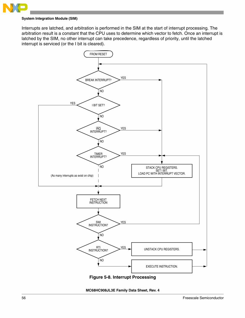
System Integration Module (SIM)
Interrupts are latched, and arbitration is performed in the SIM at the start of interrupt processing. The arbitration result is a constant that the CPU uses to determine which vector to fetch. Once an interrupt is latched by the SIM, no other interrupt can take precedence, regardless of priority, until the latched interrupt is serviced (or the I bit is cleared).
Figure 5-8. Interrupt Processing
NO
NO
NO
YES
NO
NO
YES
NO
YES
YES
(As many interrupts as exist on chip)
I BIT SET?
FROM RESET
BREAK INTERRUPT?
I BIT SET?
IRQINTERRUPT?
TIMERINTERRUPT?
SWIINSTRUCTION?
RTIINSTRUCTION?
FETCH NEXTINSTRUCTION
UNSTACK CPU REGISTERS.
STACK CPU REGISTERS.SET I BIT.
LOAD PC WITH INTERRUPT VECTOR.
EXECUTE INSTRUCTION.
YES
YES
MC68HC908JL3E Family Data Sheet, Rev. 4
56 Freescale Semiconductor

Exception Control
At the beginning of an interrupt, the CPU saves the CPU register contents on the stack and sets the interrupt mask (I bit) to prevent additional interrupts. At the end of an interrupt, the RTI instruction recovers the CPU register contents from the stack so that normal processing can resume. Figure 5-9 shows interrupt entry timing. Figure 5-10 shows interrupt recovery timing.
Figure 5-9. Interrupt Entry
Figure 5-10. Interrupt Recovery
5.5.1.1 Hardware Interrupts
A hardware interrupt does not stop the current instruction. Processing of a hardware interrupt begins after completion of the current instruction. When the current instruction is complete, the SIM checks all pending hardware interrupts. If interrupts are not masked (I bit clear in the condition code register), and if the corresponding interrupt enable bit is set, the SIM proceeds with interrupt processing; otherwise, the next instruction is fetched and executed.
If more than one interrupt is pending at the end of an instruction execution, the highest priority interrupt is serviced first. Figure 5-11 demonstrates what happens when two interrupts are pending. If an interrupt is pending upon exit from the original interrupt service routine, the pending interrupt is serviced before the LDA instruction is executed.
MODULE
IDB
R/W
INTERRUPT
DUMMY SP SP – 1 SP – 2 SP – 3 SP – 4 VECT H VECT L START ADDRIAB
DUMMY PC – 1[7:0] PC – 1[15:8] X A CCR V DATA H V DATA L OPCODE
I BIT
MODULE
IDB
R/W
INTERRUPT
SP – 4 SP – 3 SP – 2 SP – 1 SP PC PC + 1IAB
CCR A X PC – 1[15:8] PC – 1[7:0] OPCODE OPERAND
I BIT
MC68HC908JL3E Family Data Sheet, Rev. 4
Freescale Semiconductor 57

System Integration Module (SIM)
Figure 5-11. Interrupt Recognition Example
The LDA opcode is prefetched by both the INT1 and INT2 RTI instructions. However, in the case of the INT1 RTI prefetch, this is a redundant operation.
NOTETo maintain compatibility with the M6805 Family, the H register is not pushed on the stack during interrupt entry. If the interrupt service routine modifies the H register or uses the indexed addressing mode, software should save the H register and then restore it prior to exiting the routine.
5.5.1.2 SWI Instruction
The SWI instruction is a non-maskable instruction that causes an interrupt regardless of the state of the interrupt mask (I bit) in the condition code register.
NOTEA software interrupt pushes PC onto the stack. A software interrupt does not push PC – 1, as a hardware interrupt does.
5.5.2 Interrupt Status Registers
The flags in the interrupt status registers identify maskable interrupt sources. Table 5-3 summarizes the interrupt sources and the interrupt status register flags that they set. The interrupt status registers can be useful for debugging.
CLI
LDA
INT1
PULHRTI
INT2
BACKGROUND ROUTINE#$FF
PSHH
INT1 INTERRUPT SERVICE ROUTINE
PULHRTI
PSHH
INT2 INTERRUPT SERVICE ROUTINE
MC68HC908JL3E Family Data Sheet, Rev. 4
58 Freescale Semiconductor

Exception Control
5.5.2.1 Interrupt Status Register 1
IF1, IF3 to IF5 — Interrupt FlagsThese flags indicate the presence of interrupt requests from the sources shown in Table 5-3.
1 = Interrupt request present0 = No interrupt request present
Bit 0, 1, 3 and 7 — Always read 0
5.5.2.2 Interrupt Status Register 2
Table 5-3. Interrupt Sources
Priority Source Flag MASK(1)INT
Register Flag
Vector Address
Highest Reset — — — $FFFE–$FFFF
SWI Instruction — — — $FFFC–$FFFD
IRQ Pin IRQF IMASK IF1 $FFFA–$FFFB
Timer Channel 0 Interrupt CH0F CH0IE IF3 $FFF6–$FFF7
Timer Channel 1 Interrupt CH1F CH1IE IF4 $FFF4–$FFF5
Timer Overflow Interrupt TOF TOIE IF5 $FFF2–$FFF3
Keyboard Interrupt KEYF IMASKK IF14 $FFE0–$FFE1
Lowest ADC Conversion Complete Interrupt COCO AIEN IF15 $FFDE–$FFDF
1. The I bit in the condition code register is a global mask for all interrupts sources except the SWI instruction.
Address: $FE04
Bit 7 6 5 4 3 2 1 Bit 0
Read: 0 IF5 IF4 IF3 0 IF1 0 0
Write: R R R R R R R R
Reset: 0 0 0 0 0 0 0 0
R = Reserved
Figure 5-12. Interrupt Status Register 1 (INT1)
Address: $FE05
Bit 7 6 5 4 3 2 1 Bit 0
Read: IF14 0 0 0 0 0 0 0
Write: R R R R R R R R
Reset: 0 0 0 0 0 0 0 0
R = Reserved
Figure 5-13. Interrupt Status Register 2 (INT2)
MC68HC908JL3E Family Data Sheet, Rev. 4
Freescale Semiconductor 59

System Integration Module (SIM)
IF14 — Interrupt FlagsThis flag indicates the presence of interrupt requests from the sources shown in Table 5-3.
1 = Interrupt request present0 = No interrupt request present
Bit 0 to 6 — Always read 0
5.5.2.3 Interrupt Status Register 3
IF15 — Interrupt FlagsThese flags indicate the presence of interrupt requests from the sources shown in Table 5-3.
1 = Interrupt request present0 = No interrupt request present
Bit 1 to 7 — Always read 0
5.5.3 Reset
All reset sources always have equal and highest priority and cannot be arbitrated.
5.5.4 Break Interrupts
The break module can stop normal program flow at a software-programmable break point by asserting its break interrupt output. (See Chapter 15 Break Module (BREAK).) The SIM puts the CPU into the break state by forcing it to the SWI vector location. Refer to the break interrupt subsection of each module to see how each module is affected by the break state.
5.5.5 Status Flag Protection in Break Mode
The SIM controls whether status flags contained in other modules can be cleared during break mode. The user can select whether flags are protected from being cleared by properly initializing the break clear flag enable bit (BCFE) in the break flag control register (BFCR).
Protecting flags in break mode ensures that set flags will not be cleared while in break mode. This protection allows registers to be freely read and written during break mode without losing status flag information.
Setting the BCFE bit enables the clearing mechanisms. Once cleared in break mode, a flag remains cleared even when break mode is exited. Status flags with a two-step clearing mechanism — for example, a read of one register followed by the read or write of another — are protected, even when the first step is accomplished prior to entering break mode. Upon leaving break mode, execution of the second step will clear the flag as normal.
Address: $FE06
Bit 7 6 5 4 3 2 1 Bit 0
Read: 0 0 0 0 0 0 0 IF15
Write: R R R R R R R R
Reset: 0 0 0 0 0 0 0 0
R = Reserved
Figure 5-14. Interrupt Status Register 3 (INT3)
MC68HC908JL3E Family Data Sheet, Rev. 4
60 Freescale Semiconductor

Low-Power Modes
5.6 Low-Power Modes
Executing the WAIT or STOP instruction puts the MCU in a low-power-consumption mode for standby situations. The SIM holds the CPU in a non-clocked state. The operation of each of these modes is described below. Both STOP and WAIT clear the interrupt mask (I) in the condition code register, allowing interrupts to occur.
5.6.1 Wait Mode
In wait mode, the CPU clocks are inactive while the peripheral clocks continue to run. Figure 5-15 shows the timing for wait mode entry.
A module that is active during wait mode can wake up the CPU with an interrupt if the interrupt is enabled. Stacking for the interrupt begins one cycle after the WAIT instruction during which the interrupt occurred. In wait mode, the CPU clocks are inactive. Refer to the wait mode subsection of each module to see if the module is active or inactive in wait mode. Some modules can be programmed to be active in wait mode.
Wait mode can also be exited by a reset or break. A break interrupt during wait mode sets the SIM break stop/wait bit, SBSW, in the break status register (BSR). If the COP disable bit, COPD, in the mask option register is zero, then the computer operating properly module (COP) is enabled and remains active in wait mode.
Figure 5-15. Wait Mode Entry Timing
Figure 5-16 and Figure 5-17 show the timing for WAIT recovery.
Figure 5-16. Wait Recovery from Interrupt or Break
WAIT ADDR + 1 SAME SAMEIAB
IDB PREVIOUS DATA NEXT OPCODE SAME
WAIT ADDR
SAME
R/W
NOTE: Previous data can be operand data or the WAIT opcode, depending on the last instruction.
$6E0C$6E0B $00FF $00FE $00FD $00FC
$A6 $A6 $01 $0B $6E$A6
IAB
IDB
EXITSTOPWAIT
NOTE: EXITSTOPWAIT = RST pin OR CPU interrupt OR break interrupt
MC68HC908JL3E Family Data Sheet, Rev. 4
Freescale Semiconductor 61

System Integration Module (SIM)
Figure 5-17. Wait Recovery from Internal Reset
5.6.2 Stop Mode
In stop mode, the SIM counter is reset and the system clocks are disabled. An interrupt request from a module can cause an exit from stop mode. Stacking for interrupts begins after the selected stop recovery time has elapsed. Reset or break also causes an exit from stop mode.
The SIM disables the oscillator signals (OSCOUT and 2OSCOUT) in stop mode, stopping the CPU and peripherals. Stop recovery time is selectable using the SSREC bit in the configuration register (CONFIG). If SSREC is set, stop recovery is reduced from the normal delay of 4096 2OSCOUT cycles down to 32. This is ideal for applications using canned oscillators that do not require long start-up times from stop mode.
NOTEExternal crystal applications should use the full stop recovery time by clearing the SSREC bit.
A break interrupt during stop mode sets the SIM break stop/wait bit (SBSW) in the break status register (BSR).
The SIM counter is held in reset from the execution of the STOP instruction until the beginning of stop recovery. It is then used to time the recovery period. Figure 5-18 shows stop mode entry timing.
NOTETo minimize stop current, all pins configured as inputs should be driven to a logic 1 or logic 0.
Figure 5-18. Stop Mode Entry Timing
IAB
IDB
RST
$A6 $A6
$6E0B RST VCT H RST VCT L
$A6
2OSCOUT
32Cycles
32Cycles
STOP ADDR + 1 SAME SAMEIAB
IDB PREVIOUS DATA NEXT OPCODE SAME
STOP ADDR
SAME
R/W
CPUSTOP
NOTE: Previous data can be operand data or the STOP opcode, depending on the last instruction.
MC68HC908JL3E Family Data Sheet, Rev. 4
62 Freescale Semiconductor

SIM Registers
Figure 5-19. Stop Mode Recovery from Interrupt or Break
5.7 SIM Registers
The SIM has three memory mapped registers. Table 5-4 shows the mapping of these registers.
5.7.1 Break Status Register (BSR)
The break status register contains a flag to indicate a break caused by an exit from wait mode.
SBSW — SIM Break Stop/WaitSBSW can be read within the break state SWI routine. The user can modify the return address on the stack by subtracting one from it.
1 = Wait mode was exited by break interrupt0 = Wait mode was not exited by break interrupt
Table 5-4. SIM Registers
Address Register Access Mode
$FE00 BSR User
$FE01 RSR User
$FE03 BFCR User
Address: $FE00
Bit 7 6 5 4 3 2 1 Bit 0
Read:R R R R R R
SBSWR
Write: Note(1)
Reset: 0
R = Reserved 1. Writing a zero clears SBSW.
Figure 5-20. Break Status Register (BSR)
2OSCOUT
INT/BREAK
IAB STOP + 2 STOP + 2 SP SP – 1 SP – 2 SP – 3STOP +1
STOP RECOVERY PERIOD
MC68HC908JL3E Family Data Sheet, Rev. 4
Freescale Semiconductor 63

System Integration Module (SIM)
5.7.2 Reset Status Register (RSR)
The SRSR register contains flags that show the source of the last reset. The status register will automatically clear after reading SRSR. A power-on reset sets the POR bit and clears all other bits in the register. All other reset sources set the individual flag bits but do not clear the register. More than one reset source can be flagged at any time depending on the conditions at the time of the internal or external reset. For example, the POR and LVI bit can both be set if the power supply has a slow rise time.
POR — Power-On Reset Bit1 = Last reset caused by POR circuit0 = Read of SRSR
PIN — External Reset Bit1 = Last reset caused by external reset pin (RST)0 = POR or read of SRSR
COP — Computer Operating Properly Reset Bit1 = Last reset caused by COP counter0 = POR or read of SRSR
ILOP — Illegal Opcode Reset Bit1 = Last reset caused by an illegal opcode0 = POR or read of SRSR
ILAD — Illegal Address Reset Bit (opcode fetches only)1 = Last reset caused by an opcode fetch from an illegal address0 = POR or read of SRSR
MODRST — Monitor Mode Entry Module Reset bit1 = Last reset caused by monitor mode entry when vector locations $FFFE and $FFFF are $FF after
POR while IRQ = VDD0 = POR or read of SRSR
LVI — Low Voltage Inhibit Reset bit1 = Last reset caused by LVI circuit0 = POR or read of SRSR
Address: $FE01
Bit 7 6 5 4 3 2 1 Bit 0
Read: POR PIN COP ILOP ILAD MODRST LVI 0
Write:
POR: 1 0 0 0 0 0 0 0
= Unimplemented
Figure 5-21. Reset Status Register (RSR)
MC68HC908JL3E Family Data Sheet, Rev. 4
64 Freescale Semiconductor

SIM Registers
5.7.3 Break Flag Control Register (BFCR)
The break control register contains a bit that enables software to clear status bits while the MCU is in a break state.
BCFE — Break Clear Flag Enable BitThis read/write bit enables software to clear status bits by accessing status registers while the MCU is in a break state. To clear status bits during the break state, the BCFE bit must be set.
1 = Status bits clearable during break0 = Status bits not clearable during break
Address: $FE03
Bit 7 6 5 4 3 2 1 Bit 0
Read:BCFE R R R R R R R
Write:
Reset: 0
R = Reserved
Figure 5-22. Break Flag Control Register (BFCR)
MC68HC908JL3E Family Data Sheet, Rev. 4
Freescale Semiconductor 65

System Integration Module (SIM)
MC68HC908JL3E Family Data Sheet, Rev. 4
66 Freescale Semiconductor

Chapter 6 Oscillator (OSC)
6.1 Introduction
The oscillator module provides the reference clock for the MCU system and bus. Two types of oscillator modules are available:
• MC68HC908JL3E/JK3E/JK1E — built-in oscillator module (X-tal) that requires an external crystal or ceramic-resonator. This option also allows an external clock that can be driven directly into OSC1.
• MC68HRC908JL3E/JK3E/JK1E — built-in oscillator module (RC) that requires an external RC connection only.
6.2 X-tal Oscillator (MC68HC908JL3E/JK3E/JK1E)
The X-tal oscillator circuit is designed for use with an external crystal or ceramic resonator to provide accurate clock source.
In its typical configuration, the X-tal oscillator is connected in a Pierce oscillator configuration, as shown in Figure 6-1. This figure shows only the logical representation of the internal components and may not represent actual circuitry. The oscillator configuration uses five components:
• Crystal, X1• Fixed capacitor, C1• Tuning capacitor, C2 (can also be a fixed capacitor)• Feedback resistor, RB
• Series resistor, RS (optional)
The series resistor (RS) is included in the diagram to follow strict Pierce oscillator guidelines and may not be required for all ranges of operation, especially with high frequency crystals. Refer to the crystal manufacturer’s data for more information.
6.3 RC Oscillator (MC68HRC908JL3E/JK3E/JK1E)
The RC oscillator circuit is designed for use with external R and C to provide a clock source with tolerance less than 10%.
In its typical configuration, the RC oscillator requires two external components, one R and one C. Component values should have a tolerance of 1% or less, to obtain a clock source with less than 10% tolerance. The oscillator configuration uses two components:
• CEXT• REXT
The RC connection is shown in Figure 6-2.
MC68HC908JL3E Family Data Sheet, Rev. 4
Freescale Semiconductor 67

Oscillator (OSC)
Figure 6-1. X-tal Oscillator External Connections
Figure 6-2. RC Oscillator External Connections
C1 C2
SIMOSCEN
XTALCLK
RB
X1
RS*
*RS can be zero (shorted) when used with higher-frequency crystals.
MCU
From SIM
Refer to manufacturer’s data.
OSC2OSC1
÷ 2
OSCOUT2OSCOUT
To SIMTo SIM
See Chapter 16 Electrical Specifications for componentvalue requirements.
MCU
REXT CEXT
SIMOSCEN
OSC1
Ext-RCOscillator
ENRCCLK
÷ 2
OSCOUT2OSCOUT
To SIMFrom SIM
VDD
PTA6I/O
0
1 PTA6
PTA6EN
PTA6/RCCLK (OSC2)
To SIM
See Chapter 16 Electrical Specifications for componentvalue requirements.
MC68HC908JL3E Family Data Sheet, Rev. 4
68 Freescale Semiconductor

I/O Signals
6.4 I/O Signals
The following paragraphs describe the oscillator I/O signals.
6.4.1 Crystal Amplifier Input Pin (OSC1)
OSC1 pin is an input to the crystal oscillator amplifier or the input to the RC oscillator circuit.
6.4.2 Crystal Amplifier Output Pin (OSC2/PTA6/RCCLK)
For the X-tal oscillator device, OSC2 pin is the output of the crystal oscillator inverting amplifier.
For the RC oscillator device, OSC2 pin can be configured as a general purpose I/O pin PTA6, or the output of the internal RC oscillator clock, RCCLK.
6.4.3 Oscillator Enable Signal (SIMOSCEN)
The SIMOSCEN signal comes from the system integration module (SIM) and enables/disables the X-tal oscillator circuit or the RC-oscillator.
6.4.4 X-tal Oscillator Clock (XTALCLK)
XTALCLK is the X-tal oscillator output signal. It runs at the full speed of the crystal (fXCLK) and comes directly from the crystal oscillator circuit. Figure 6-1 shows only the logical relation of XTALCLK to OSC1 and OSC2 and may not represent the actual circuitry. The duty cycle of XTALCLK is unknown and may depend on the crystal and other external factors. Also, the frequency and amplitude of XTALCLK can be unstable at start-up.
6.4.5 RC Oscillator Clock (RCCLK)
RCCLK is the RC oscillator output signal. Its frequency is directly proportional to the time constant of the external R and C. Figure 6-2 shows only the logical relation of RCCLK to OSC1 and may not represent the actual circuitry.
6.4.6 Oscillator Out 2 (2OSCOUT)
2OSCOUT is same as the input clock (XTALCLK or RCCLK). This signal is driven to the SIM module and is used to determine the COP cycles.
6.4.7 Oscillator Out (OSCOUT)
The frequency of this signal is equal to half of the 2OSCOUT, this signal is driven to the SIM for generation of the bus clocks used by the CPU and other modules on the MCU. OSCOUT will be divided again in the SIM and results in the internal bus frequency being one fourth of the XTALCLK or RCCLK frequency.
Device Oscillator OSC2 pin function
MC68HC908JL3E/JK3E/JK1E X-tal Inverting OSC1
MC68HRC908JL3E/JK3E/JK1E RCControlled by PTA6EN bit in PTAPUER ($0D)
PTA6EN = 0: RCCLK outputPTA6EN = 1: PTA6 I/O
MC68HC908JL3E Family Data Sheet, Rev. 4
Freescale Semiconductor 69

Oscillator (OSC)
6.5 Low Power Modes
The WAIT and STOP instructions put the MCU in low-power consumption standby modes.
6.5.1 Wait Mode
The WAIT instruction has no effect on the oscillator logic. OSCOUT and 2OSCOUT continues to drive to the SIM module.
6.5.2 Stop Mode
The STOP instruction disables the XTALCLK or the RCCLK output, hence OSCOUT and 2OSCOUT.
6.6 Oscillator During Break Mode
The oscillator continues to drive OSCOUT and 2OSCOUT when the device enters the break state.
MC68HC908JL3E Family Data Sheet, Rev. 4
70 Freescale Semiconductor

Chapter 7 Monitor ROM (MON)
7.1 Introduction
This section describes the monitor ROM (MON) and the monitor mode entry methods. The monitor ROM allows complete testing of the MCU through a single-wire interface with a host computer. This mode is also used for programming and erasing of Flash memory in the MCU. Monitor mode entry can be achieved without use of the higher test voltage, VTST, as long as vector addresses $FFFE and $FFFF are blank, thus reducing the hardware requirements for in-circuit programming.
7.2 Features
Features of the monitor ROM include the following:• Normal user-mode pin functionality• One pin dedicated to serial communication between monitor ROM and host computer• Standard mark/space non-return-to-zero (NRZ) communication with host computer• Execution of code in RAM or Flash• Flash memory security feature(1)
• Flash memory programming interface• 960 bytes monitor ROM code size• Monitor mode entry without high voltage, VTST, if reset vector is blank ($FFFE and $FFFF contain
$FF)• Standard monitor mode entry if high voltage, VTST, is applied to IRQ
7.3 Functional Description
The monitor ROM receives and executes commands from a host computer. Figure 7-1 shows a example circuit used to enter monitor mode and communicate with a host computer via a standard RS-232 interface.
Simple monitor commands can access any memory address. In monitor mode, the MCU can execute host-computer code in RAM while most MCU pins retain normal operating mode functions. All communication between the host computer and the MCU is through the PTB0 pin. A level-shifting and multiplexing interface is required between PTB0 and the host computer. PTB0 is used in a wired-OR configuration and requires a pull-up resistor.
1. No security feature is absolutely secure. However, Freescale’s strategy is to make reading or copying the Flash difficult for unauthorized users.
MC68HC908JL3E Family Data Sheet, Rev. 4
Freescale Semiconductor 71

Monitor ROM (MON)
Figure 7-1. Monitor Mode Circuit
NOTES:1. Monitor mode entry method:
SW1: Position A — High voltage entry (VTST)Clock source must be EXT OSC or XTAL CIRCUIT.Bus clock depends on SW2.
SW1: Position B — Reset vector must be blank ($FFFE = $FFFF = $FF)Bus clock = OSC1 ÷ 4.
2. Affects high voltage entry to monitor mode only (SW1 at position A):SW2: Position C — Bus clock = OSC1 ÷ 4SW2: Position D — Bus clock = OSC1 ÷ 2
5. See Table 16-4. DC Electrical Characteristics (5V) for VTST voltage level requirements.
10M
RST
IRQ
OSC1
OSC2
VSS
PTB0
20 pF
20 pF
0.1 μF
9.8304MHz
PTB1
VDD
0.1 μF
VDD
PTB2
VDD
10 k
PTB3
VDD
10 k
10 k
SW2C
D
VDD
(SEE NOTE 2)
A
B
XTAL CIRCUIT
16
15
2
6VDD
MAX232
V+
V–
VDD
10 k
C1+
C1–
5
4 C2+
C2–
+
3
1
1 μF+ +
+
8
7DB9
2
3
5
10
9
+
1
2 3 4
5674HC125
74HC125
1 k
VTST
VCC
GND
1 μF
1 μF
1 μF
1 μF
8.5 V VDD10 k
10 k
(50% DUTY)
OSC1
(SEE NOTE 1)SW1
VDD
OSC1
OSC2
See Figure 16-1. RC vs. Frequency (5V @25°C) for component values vs. frequency.
H(R)C908JL3EH(R)C908JK3EH(R)C908JK1E
EXT OSC
OSC2
RC CIRCUIT
FOR MC68HC908JL3E/JK3E/JK1ESW1 AT POSITION A OR B
FOR MC68HRC908JL3E/JK3E/JK1ESW1 MUST BE AT POSITION A
FOR MC68HC908JL3E/JK3E/JK1ESW1 AT POSITION A OR B
FOR MC68HRC908JL3E/JK3E/JK1ESW1 MUST BE AT POSITION B
MC68HC908JL3E Family Data Sheet, Rev. 4
72 Freescale Semiconductor

Functional Description
7.3.1 Entering Monitor Mode
Table 7-1 shows the pin conditions for entering monitor mode. As specified in the table, monitor mode may be entered after a POR and will allow communication at 9600 baud provided one of the following sets of conditions is met:
1. If IRQ = VTST:– Clock on OSC1 is 4.9125MHz (EXT OSC or XTAL)– PTB3 = low
2. If IRQ = VTST:– Clock on OSC1 is 9.8304MHz (EXT OSC or XTAL)– PTB3 = high
3. If $FFFE & $FFFF is blank (contains $FF):– Clock on OSC1 is 9.8304MHz (EXT OSC or XTAL or RC)– IRQ = VDD
If VTST is applied to IRQ and PTB3 is low upon monitor mode entry (Table 7-1 condition set 1), the bus frequency is a divide-by-two of the clock input to OSC1. If PTB3 is high with VTST applied to IRQ upon monitor mode entry (Table 7-1 condition set 2), the bus frequency is a divide-by-four of the clock input to OSC1. Holding the PTB3 pin low when entering monitor mode causes a bypass of a divide-by-two stage at the oscillator only if VTST is applied to IRQ. In this event, the OSCOUT frequency is equal to the 2OSCOUT frequency, and OSC1 input directly generates internal bus clocks. In this case, the OSC1 signal must have a 50% duty cycle at maximum bus frequency.
Table 7-1. Monitor Mode Entry Requirements and Options
IRQ
$FF
FE
and
$FF
FF
PT
B3(1
)
1. PTB3 = 0: Bypasses the divide-by-two prescaler to SIM when using VTST for monitor mode entry.The OSC1 clock must be 50% duty cycle for this condition.
PT
B2
PT
B1
PT
B0
OSC1 FrequencyBus
FrequencyComments
VTST(2)
2. See Table 16-4. DC Electrical Characteristics (5V) for VTST voltage level requirements.
X 0 0 1 1 4.9152MHz2.4576MHz(OSC1 ÷ 2)
High-voltage entry to monitor mode.(3)
9600 baud communication on PTB0. COP disabled.
3. For IRQ = VTST:MC68HRC908JL3E/JK3E/JK1E — clock must be EXT OSC.MC68HC908JL3E/JK3E/JK1E — clock can be EXT OSC or XTAL.
VTST X 1 0 1 1 9.8304MHz2.4576MHz(OSC1 ÷ 4)
VDD
BLANK(contain
$FF)X X X 1 9.8304MHz
2.4576MHz(OSC1 ÷ 4)
Low-voltage entry to monitor mode.(4)
9600 baud communication on PTB0. COP disabled.
4. For IRQ = VDD:MC68HRC908JL3E/JK3E/JK1E — clock must be RC OSC.MC68HC908JL3E/JK3E/JK1E — clock can be EXT OSC or XTAL.
VDDNOT
BLANKX X X X
At desired frequency
OSC1 ÷ 4 Enters User mode.
MC68HC908JL3E Family Data Sheet, Rev. 4
Freescale Semiconductor 73

Monitor ROM (MON)
Entering monitor mode with VTST on IRQ, the COP is disabled as long as VTST is applied to either the IRQ or the RST. (See Chapter 5 System Integration Module (SIM) for more information on modes of operation.)
If entering monitor mode without high voltage on IRQ and reset vector being blank ($FFFE and $FFFF) (Table 7-1 condition set 3, where applied voltage is VDD), then all port B pin requirements and conditions, including the PTB3 frequency divisor selection, are not in effect. This is to reduce circuit requirements when performing in-circuit programming.
Entering monitor mode with the reset vector being blank, the COP is always disabled regardless of the state of IRQ or the RST.
Figure 7-2. shows a simplified diagram of the monitor mode entry when the reset vector is blank and IRQ = VDD. An OSC1 frequency of 9.8304MHz is required for a baud rate of 9600.
Figure 7-2. Low-Voltage Monitor Mode Entry Flowchart
Enter monitor mode with the pin configuration shown above by pulling RST low and then high. The rising edge of RST latches monitor mode. Once monitor mode is latched, the values on the specified pins can change.
Once out of reset, the MCU waits for the host to send eight security bytes. (See 7.4 Security.) After the security bytes, the MCU sends a break signal (10 consecutive logic zeros) to the host, indicating that it is ready to receive a command. The break signal also provides a timing reference to allow the host to determine the necessary baud rate.
In monitor mode, the MCU uses different vectors for reset, SWI, and break interrupt. The alternate vectors are in the $FE page instead of the $FF page and allow code execution from the internal monitor firmware instead of user code.
IS VECTORBLANK?
PORTRIGGERED?
NORMAL USERMODE
MONITOR MODE
EXECUTEMONITOR
CODE
NO
NO
YES
YES
POR RESET
MC68HC908JL3E Family Data Sheet, Rev. 4
74 Freescale Semiconductor

Functional Description
Table 7-2 is a summary of the vector differences between user mode and monitor mode.
When the host computer has completed downloading code into the MCU RAM, the host then sends a RUN command, which executes an RTI, which sends control to the address on the stack pointer.
7.3.2 Baud Rate
The communication baud rate is dependant on oscillator frequency. The state of PTB3 also affects baud rate if entry to monitor mode is by IRQ = VTST. When PTB3 is high, the divide by ratio is 1024. If the PTB3 pin is at logic zero upon entry into monitor mode, the divide by ratio is 512.
Table 7-2. Monitor Mode Vector Differences
Modes
Functions
COPResetVectorHigh
ResetVectorLow
BreakVectorHigh
BreakVectorLow
SWIVectorHigh
SWIVector
Low
User Enabled $FFFE $FFFF $FFFC $FFFD $FFFC $FFFD
Monitor Disabled(1) $FEFE $FEFF $FEFC $FEFD $FEFC $FEFD
1. If the high voltage (VTST) is removed from the IRQ pin or the RST pin, the SIM assertsits COP enable output. The COP is a mask option enabled or disabled by the COPD bitin the configuration register.
Table 7-3. Monitor Baud Rate Selection
Monitor ModeEntry By:
Input Clock Frequency
PTB3 Baud Rate
IRQ = VTST
4.9152 MHz 0 9600 bps
9.8304 MHz 1 9600 bps
4.9152 MHz 1 4800 bps
Blank reset vector,IRQ = VDD
9.8304 MHz X 9600 bps
4.9152 MHz X 4800 bps
MC68HC908JL3E Family Data Sheet, Rev. 4
Freescale Semiconductor 75

Monitor ROM (MON)
7.3.3 Data Format
Communication with the monitor ROM is in standard non-return-to-zero (NRZ) mark/space data format. (See Figure 7-3 and Figure 7-4.)
Figure 7-3. Monitor Data Format
Figure 7-4. Sample Monitor Waveforms
The data transmit and receive rate can be anywhere from 4800 baud to 28.8k-baud. Transmit and receive baud rates must be identical.
7.3.4 Echoing
As shown in Figure 7-5, the monitor ROM immediately echoes each received byte back to the PTB0 pin for error checking.
Figure 7-5. Read Transaction
Any result of a command appears after the echo of the last byte of the command.
7.3.5 Break Signal
A start bit followed by nine low bits is a break signal. (See Figure 7-6.) When the monitor receives a break signal, it drives the PTB0 pin high for the duration of two bits before echoing the break signal.
Figure 7-6. Break Transaction
BIT 5START
BIT BIT 0 BIT 1
NEXT
STOPBIT
STARTBITBIT 2 BIT 3 BIT 4 BIT 6 BIT 7
BIT 5START
BIT BIT 0 BIT 1
NEXT
STOPBIT
STARTBITBIT 2 BIT 3 BIT 4 BIT 6 BIT 7
STARTBIT BIT 0 BIT 1 NEXT
STOPBIT
STARTBIT
BIT 2
$A5
BREAK BIT 3 BIT 4 BIT 5 BIT 6 BIT 7
ADDR. HIGHREADREAD ADDR. HIGH ADDR. LOW ADDR. LOW DATA
ECHO
SENT TOMONITOR
RESULT
0 1 2 3 4 5 6 7 0 1 2 3 4 5 6 7
MISSING STOP BITTWO-STOP-BIT DELAY BEFORE ZERO ECHO
MC68HC908JL3E Family Data Sheet, Rev. 4
76 Freescale Semiconductor

Functional Description
7.3.6 Commands
The monitor ROM uses the following commands:• READ (read memory)• WRITE (write memory)• IREAD (indexed read)• IWRITE (indexed write)• READSP (read stack pointer)• RUN (run user program)
Table 7-4. READ (Read Memory) Command
Description Read byte from memory
Operand Specifies 2-byte address in high byte:low byte order
Data Returned Returns contents of specified address
Opcode $4A
Command Sequence
Table 7-5. WRITE (Write Memory) Command
Description Write byte to memory
Operand Specifies 2-byte address in high byte:low byte order; low byte followed by data byte
Data Returned None
Opcode $49
Command Sequence
ADDR. HIGHREADREAD ADDR. HIGH ADDR. LOW ADDR. LOW DATA
ECHO
SENT TOMONITOR
RESULT
ADDR. HIGHWRITEWRITE ADDR. HIGH ADDR. LOW ADDR. LOW DATA
ECHO
SENT TOMONITOR
DATA
MC68HC908JL3E Family Data Sheet, Rev. 4
Freescale Semiconductor 77
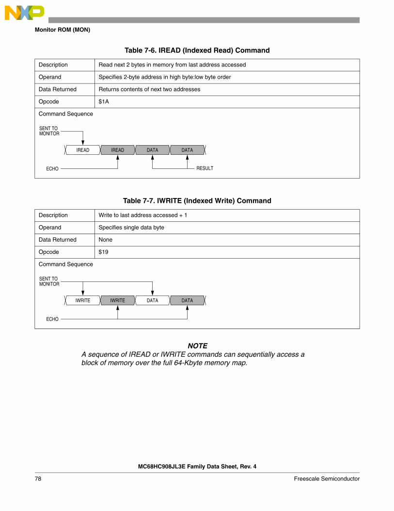
Monitor ROM (MON)
NOTEA sequence of IREAD or IWRITE commands can sequentially access a block of memory over the full 64-Kbyte memory map.
Table 7-6. IREAD (Indexed Read) Command
Description Read next 2 bytes in memory from last address accessed
Operand Specifies 2-byte address in high byte:low byte order
Data Returned Returns contents of next two addresses
Opcode $1A
Command Sequence
Table 7-7. IWRITE (Indexed Write) Command
Description Write to last address accessed + 1
Operand Specifies single data byte
Data Returned None
Opcode $19
Command Sequence
DATAIREADIREAD DATA
ECHO
SENT TOMONITOR
RESULT
DATAIWRITEIWRITE DATA
ECHO
SENT TOMONITOR
MC68HC908JL3E Family Data Sheet, Rev. 4
78 Freescale Semiconductor

Security
7.4 Security
A security feature discourages unauthorized reading of Flash locations while in monitor mode. The host can bypass the security feature at monitor mode entry by sending eight security bytes that match the bytes at locations $FFF6–$FFFD. Locations $FFF6–$FFFD contain user-defined data.
NOTEDo not leave locations $FFF6–$FFFD blank. For security reasons, program locations $FFF6–$FFFD even if they are not used for vectors.
During monitor mode entry, the MCU waits after the power-on reset for the host to send the eight security bytes on pin PTB0. If the received bytes match those at locations $FFF6–$FFFD, the host bypasses the security feature and can read all Flash locations and execute code from Flash. Security remains bypassed until a power-on reset occurs. If the reset was not a power-on reset, security remains bypassed and security code entry is not required. (See Figure 7-7.)
Table 7-8. READSP (Read Stack Pointer) Command
Description Reads stack pointer
Operand None
Data Returned Returns stack pointer in high byte:low byte order
Opcode $0C
Command Sequence
Table 7-9. RUN (Run User Program) Command
Description Executes RTI instruction
Operand None
Data Returned None
Opcode $28
Command Sequence
SP HIGHREADSPREADSP SP LOW
ECHO
SENT TOMONITOR
RESULT
RUNRUN
ECHO
SENT TOMONITOR
MC68HC908JL3E Family Data Sheet, Rev. 4
Freescale Semiconductor 79

Monitor ROM (MON)
Figure 7-7. Monitor Mode Entry Timing
Upon power-on reset, if the received bytes of the security code do not match the data at locations $FFF6–$FFFD, the host fails to bypass the security feature. The MCU remains in monitor mode, but reading a Flash location returns an invalid value and trying to execute code from Flash causes an illegal address reset. After receiving the eight security bytes from the host, the MCU transmits a break character, signifying that it is ready to receive a command.
NOTEThe MCU does not transmit a break character until after the host sends the eight security bytes.
To determine whether the security code entered is correct, check to see if bit 6 of RAM address $80 is set. If it is, then the correct security code has been entered and Flash can be accessed.
If the security sequence fails, the device should be reset by a power-on reset and brought up in monitor mode to attempt another entry. After failing the security sequence, the Flash module can also be mass erased by executing an erase routine that was downloaded into internal RAM. The mass erase operation clears the security code locations so that all eight security bytes become $FF (blank).
BY
TE
1
BY
TE
1 E
CH
O
BY
TE
2
BY
TE
2 E
CH
O
BY
TE
8
BY
TE
8 E
CH
O
CO
MM
AN
D
CO
MM
AN
D E
CH
O
PTB0
RST
VDD
4096 + 32 OSCXCLK CYCLES
24 BUS CYCLES
1 4 1 1 2 1
BR
EA
K
NOTES:
2 = Data return delay, 2 bit times4 = Wait 1 bit time before sending next byte.
4
FROM HOST
FROM MCU
1 = Echo delay, 2 bit times
MC68HC908JL3E Family Data Sheet, Rev. 4
80 Freescale Semiconductor
Chapter 8 Timer Interface Module (TIM)
8.1 Introduction
This section describes the timer interface module (TIM2, Version B). The TIM is a two-channel timer that provides a timing reference with input capture, output compare, and pulse-width-modulation functions. Figure 8-1 is a block diagram of the TIM.
8.2 Features
Features of the TIM include the following:• Two input capture/output compare channels
– Rising-edge, falling-edge, or any-edge input capture trigger– Set, clear, or toggle output compare action
• Buffered and unbuffered pulse width modulation (PWM) signal generation• Programmable TIM clock input with 7-frequency internal bus clock prescaler selection• Free-running or modulo up-count operation• Toggle any channel pin on overflow• TIM counter stop and reset bits
8.3 Pin Name Conventions
The TIM share two I/O pins with two port D I/O pins. The full name of the TIM I/O pins are listed inTable 8-1. The generic pin name appear in the text that follows.
Table 8-1. Pin Name Conventions
TIM Generic Pin Names: TCH0 TCH1
Full TIM Pin Names: PTD4/TCH0 PTD5/TCH1
MC68HC908JL3E Family Data Sheet, Rev. 4
Freescale Semiconductor 81

Timer Interface Module (TIM)
8.4 Functional Description
Figure 8-1 shows the structure of the TIM. The central component of the TIM is the 16-bit TIM counter that can operate as a free-running counter or a modulo up-counter. The TIM counter provides the timing reference for the input capture and output compare functions. The TIM counter modulo registers, TMODH:TMODL, control the modulo value of the TIM counter. Software can read the TIM counter value at any time without affecting the counting sequence.
The two TIM channels are programmable independently as input capture or output compare channels.
Figure 8-1. TIM Block Diagram
PRESCALER
PRESCALER SELECT
16-BIT COMPARATOR
PS2 PS1 PS0
16-BIT COMPARATOR
16-BIT LATCH
TCH0H:TCH0L
MS0A
ELS0B ELS0A
TOF
TOIE
16-BIT COMPARATOR
16-BIT LATCH
TCH1H:TCH1L
CHANNEL 0
CHANNEL 1
TMODH:TMODL
TRST
TSTOP
TOV0
CH0IE
CH0F
ELS1B ELS1ATOV1
CH1IE
CH1MAX
CH1F
CH0MAX
MS0B
16-BIT COUNTER
INTE
RN
AL B
US
MS1A
INTERNALBUS CLOCK
TCH1
TCH0
INTERRUPTLOGIC
PORTLOGIC
INTERRUPTLOGIC
INTERRUPTLOGIC
PORTLOGIC
MC68HC908JL3E Family Data Sheet, Rev. 4
82 Freescale Semiconductor

Functional Description
Addr. Register Name Bit 7 6 5 4 3 2 1 Bit 0
$0020TIM Status and Control
Register (TSC)
Read: TOFTOIE TSTOP
0 0PS2 PS1 PS0
Write: 0 TRST
Reset: 0 0 1 0 0 0 0 0
$0021TIM Counter Register High
(TCNTH)
Read: Bit15 Bit14 Bit13 Bit12 Bit11 Bit10 Bit9 Bit8
Write:
Reset: 0 0 0 0 0 0 0 0
$0022TIM Counter Register Low
(TCNTL)
Read: Bit7 Bit6 Bit5 Bit4 Bit3 Bit2 Bit1 Bit0
Write:
Reset: 0 0 0 0 0 0 0 0
$0023TIM Counter Modulo Register
High (TMODH)
Read:Bit15 Bit14 Bit13 Bit12 Bit11 Bit10 Bit9 Bit8
Write:
Reset: 1 1 1 1 1 1 1 1
$0024TIM Counter Modulo Register
Low (TMODL)
Read:Bit7 Bit6 Bit5 Bit4 Bit3 Bit2 Bit1 Bit0
Write:
Reset: 1 1 1 1 1 1 1 1
$0025TIM Channel 0 Status and
Control Register (TSC0)
Read: CH0FCH0IE MS0B MS0A ELS0B ELS0A TOV0 CH0MAX
Write: 0
Reset: 0 0 0 0 0 0 0 0
$0026TIM Channel 0 Register High
(TCH0H)
Read:Bit15 Bit14 Bit13 Bit12 Bit11 Bit10 Bit9 Bit8
Write:
Reset: Indeterminate after reset
$0027TIM Channel 0 Register Low
(TCH0L)
Read:Bit7 Bit6 Bit5 Bit4 Bit3 Bit2 Bit1 Bit0
Write:
Reset: Indeterminate after reset
$0028TIM Channel 1 Status and
Control Register (TSC1)
Read: CH1FCH1IE
0MS1A ELS1B ELS1A TOV1 CH1MAX
Write: 0
Reset: 0 0 0 0 0 0 0 0
$0029TIM Channel 1 Register High
(TCH1H)
Read:Bit15 Bit14 Bit13 Bit12 Bit11 Bit10 Bit9 Bit8
Write:
Reset: Indeterminate after reset
$002ATIM Channel 1 Register Low
(TCH1L)
Read:Bit7 Bit6 Bit5 Bit4 Bit3 Bit2 Bit1 Bit0
Write:
Reset: Indeterminate after reset
= Unimplemented
Figure 8-2. TIM I/O Register Summary
MC68HC908JL3E Family Data Sheet, Rev. 4
Freescale Semiconductor 83

Timer Interface Module (TIM)
8.4.1 TIM Counter Prescaler
The TIM clock source is one of the seven prescaler outputs. The prescaler generates seven clock rates from the internal bus clock. The prescaler select bits, PS[2:0], in the TIM status and control register (TSC) select the TIM clock source.
8.4.2 Input Capture
With the input capture function, the TIM can capture the time at which an external event occurs. When an active edge occurs on the pin of an input capture channel, the TIM latches the contents of the TIM counter into the TIM channel registers, TCHxH:TCHxL. The polarity of the active edge is programmable. Input captures can generate TIM CPU interrupt requests.
8.4.3 Output Compare
With the output compare function, the TIM can generate a periodic pulse with a programmable polarity, duration, and frequency. When the counter reaches the value in the registers of an output compare channel, the TIM can set, clear, or toggle the channel pin. Output compares can generate TIM CPU interrupt requests.
8.4.3.1 Unbuffered Output Compare
Any output compare channel can generate unbuffered output compare pulses as described in 8.4.3 Output Compare. The pulses are unbuffered because changing the output compare value requires writing the new value over the old value currently in the TIM channel registers.
An unsynchronized write to the TIM channel registers to change an output compare value could cause incorrect operation for up to two counter overflow periods. For example, writing a new value before the counter reaches the old value but after the counter reaches the new value prevents any compare during that counter overflow period. Also, using a TIM overflow interrupt routine to write a new, smaller output compare value may cause the compare to be missed. The TIM may pass the new value before it is written.
Use the following methods to synchronize unbuffered changes in the output compare value on channel x:• When changing to a smaller value, enable channel x output compare interrupts and write the new
value in the output compare interrupt routine. The output compare interrupt occurs at the end of the current output compare pulse. The interrupt routine has until the end of the counter overflow period to write the new value.
• When changing to a larger output compare value, enable TIM overflow interrupts and write the new value in the TIM overflow interrupt routine. The TIM overflow interrupt occurs at the end of the current counter overflow period. Writing a larger value in an output compare interrupt routine (at the end of the current pulse) could cause two output compares to occur in the same counter overflow period.
8.4.3.2 Buffered Output Compare
Channels 0 and 1 can be linked to form a buffered output compare channel whose output appears on the TCH0 pin. The TIM channel registers of the linked pair alternately control the output.
Setting the MS0B bit in TIM channel 0 status and control register (TSC0) links channel 0 and channel 1. The output compare value in the TIM channel 0 registers initially controls the output on the TCH0 pin. Writing to the TIM channel 1 registers enables the TIM channel 1 registers to synchronously control the output after the TIM overflows. At each subsequent overflow, the TIM channel registers (0 or 1) that
MC68HC908JL3E Family Data Sheet, Rev. 4
84 Freescale Semiconductor

Functional Description
control the output are the ones written to last. TSC0 controls and monitors the buffered output compare function, and TIM channel 1 status and control register (TSC1) is unused. While the MS0B bit is set, the channel 1 pin, TCH1, is available as a general-purpose I/O pin.
NOTEIn buffered output compare operation, do not write new output compare values to the currently active channel registers. User software should track the currently active channel to prevent writing a new value to the active channel. Writing to the active channel registers is the same as generating unbuffered output compares.
8.4.4 Pulse Width Modulation (PWM)
By using the toggle-on-overflow feature with an output compare channel, the TIM can generate a PWM signal. The value in the TIM counter modulo registers determines the period of the PWM signal. The channel pin toggles when the counter reaches the value in the TIM counter modulo registers. The time between overflows is the period of the PWM signal.
As Figure 8-3 shows, the output compare value in the TIM channel registers determines the pulse width of the PWM signal. The time between overflow and output compare is the pulse width. Program the TIM to clear the channel pin on output compare if the state of the PWM pulse is logic one. Program the TIM to set the pin if the state of the PWM pulse is logic zero.
Figure 8-3. PWM Period and Pulse Width
The value in the TIM counter modulo registers and the selected prescaler output determines the frequency of the PWM output. The frequency of an 8-bit PWM signal is variable in 256 increments. Writing $00FF (255) to the TIM counter modulo registers produces a PWM period of 256 times the internal bus clock period if the prescaler select value is 000 (see 8.9.1 TIM Status and Control Register (TSC)).
The value in the TIM channel registers determines the pulse width of the PWM output. The pulse width of an 8-bit PWM signal is variable in 256 increments. Writing $0080 (128) to the TIM channel registers produces a duty cycle of 128/256 or 50%.
TCHx
PERIOD
PULSEWIDTH
OVERFLOW OVERFLOW OVERFLOW
OUTPUTCOMPARE
OUTPUTCOMPARE
OUTPUTCOMPARE
MC68HC908JL3E Family Data Sheet, Rev. 4
Freescale Semiconductor 85

Timer Interface Module (TIM)
8.4.4.1 Unbuffered PWM Signal Generation
Any output compare channel can generate unbuffered PWM pulses as described in 8.4.4 Pulse Width Modulation (PWM). The pulses are unbuffered because changing the pulse width requires writing the new pulse width value over the old value currently in the TIM channel registers.
An unsynchronized write to the TIM channel registers to change a pulse width value could cause incorrect operation for up to two PWM periods. For example, writing a new value before the counter reaches the old value but after the counter reaches the new value prevents any compare during that PWM period. Also, using a TIM overflow interrupt routine to write a new, smaller pulse width value may cause the compare to be missed. The TIM may pass the new value before it is written.
Use the following methods to synchronize unbuffered changes in the PWM pulse width on channel x:• When changing to a shorter pulse width, enable channel x output compare interrupts and write the
new value in the output compare interrupt routine. The output compare interrupt occurs at the end of the current pulse. The interrupt routine has until the end of the PWM period to write the new value.
• When changing to a longer pulse width, enable TIM overflow interrupts and write the new value in the TIM overflow interrupt routine. The TIM overflow interrupt occurs at the end of the current PWM period. Writing a larger value in an output compare interrupt routine (at the end of the current pulse) could cause two output compares to occur in the same PWM period.
NOTEIn PWM signal generation, do not program the PWM channel to toggle on output compare. Toggling on output compare prevents reliable 0% duty cycle generation and removes the ability of the channel to self-correct in the event of software error or noise. Toggling on output compare also can cause incorrect PWM signal generation when changing the PWM pulse width to a new, much larger value.
8.4.4.2 Buffered PWM Signal Generation
Channels 0 and 1 can be linked to form a buffered PWM channel whose output appears on the TCH0 pin. The TIM channel registers of the linked pair alternately control the pulse width of the output.
Setting the MS0B bit in TIM channel 0 status and control register (TSC0) links channel 0 and channel 1. The TIM channel 0 registers initially control the pulse width on the TCH0 pin. Writing to the TIM channel 1 registers enables the TIM channel 1 registers to synchronously control the pulse width at the beginning of the next PWM period. At each subsequent overflow, the TIM channel registers (0 or 1) that control the pulse width are the ones written to last. TSC0 controls and monitors the buffered PWM function, and TIM channel 1 status and control register (TSC1) is unused. While the MS0B bit is set, the channel 1 pin, TCH1, is available as a general-purpose I/O pin.
NOTEIn buffered PWM signal generation, do not write new pulse width values to the currently active channel registers. User software should track the currently active channel to prevent writing a new value to the active channel. Writing to the active channel registers is the same as generating unbuffered PWM signals.
MC68HC908JL3E Family Data Sheet, Rev. 4
86 Freescale Semiconductor
Functional Description
8.4.4.3 PWM Initialization
To ensure correct operation when generating unbuffered or buffered PWM signals, use the following initialization procedure:
1. In the TIM status and control register (TSC):a. Stop the TIM counter by setting the TIM stop bit, TSTOP.
b. Reset the TIM counter and prescaler by setting the TIM reset bit, TRST.
2. In the TIM counter modulo registers (TMODH:TMODL), write the value for the required PWM period.
3. In the TIM channel x registers (TCHxH:TCHxL), write the value for the required pulse width.4. In TIM channel x status and control register (TSCx):
a. Write 0:1 (for unbuffered output compare or PWM signals) or 1:0 (for buffered output compare or PWM signals) to the mode select bits, MSxB:MSxA. (See Table 8-3.)
b. Write 1 to the toggle-on-overflow bit, TOVx.
c. Write 1:0 (to clear output on compare) or 1:1 (to set output on compare) to the edge/level select bits, ELSxB:ELSxA. The output action on compare must force the output to the complement of the pulse width level. (See Table 8-3.)
NOTEIn PWM signal generation, do not program the PWM channel to toggle on output compare. Toggling on output compare prevents reliable 0% duty cycle generation and removes the ability of the channel to self-correct in the event of software error or noise. Toggling on output compare can also cause incorrect PWM signal generation when changing the PWM pulse width to a new, much larger value.
5. In the TIM status control register (TSC), clear the TIM stop bit, TSTOP.
Setting MS0B links channels 0 and 1 and configures them for buffered PWM operation. The TIM channel 0 registers (TCH0H:TCH0L) initially control the buffered PWM output. TIM status control register 0 (TSC0) controls and monitors the PWM signal from the linked channels. MS0B takes priority over MS0A.
Clearing the toggle-on-overflow bit, TOVx, inhibits output toggles on TIM overflows. Subsequent output compares try to force the output to a state it is already in and have no effect. The result is a 0% duty cycle output.
Setting the channel x maximum duty cycle bit (CHxMAX) and setting the TOVx bit generates a 100% duty cycle output. (See 8.9.4 TIM Channel Status and Control Registers (TSC0:TSC1).)
MC68HC908JL3E Family Data Sheet, Rev. 4
Freescale Semiconductor 87

Timer Interface Module (TIM)
8.5 Interrupts
The following TIM sources can generate interrupt requests:• TIM overflow flag (TOF) — The TOF bit is set when the TIM counter reaches the modulo value
programmed in the TIM counter modulo registers. The TIM overflow interrupt enable bit, TOIE, enables TIM overflow CPU interrupt requests. TOF and TOIE are in the TIM status and control register.
• TIM channel flags (CH1F:CH0F) — The CHxF bit is set when an input capture or output compare occurs on channel x. Channel x TIM CPU interrupt requests are controlled by the channel x interrupt enable bit, CHxIE. Channel x TIM CPU interrupt requests are enabled when CHxIE=1. CHxF and CHxIE are in the TIM channel x status and control register.
8.6 Low-Power Modes
The WAIT and STOP instructions put the MCU in low power-consumption standby modes.
8.6.1 Wait Mode
The TIM remains active after the execution of a WAIT instruction. In wait mode, the TIM registers are not accessible by the CPU. Any enabled CPU interrupt request from the TIM can bring the MCU out of wait mode.
If TIM functions are not required during wait mode, reduce power consumption by stopping the TIM before executing the WAIT instruction.
8.6.2 Stop Mode
The TIM is inactive after the execution of a STOP instruction. The STOP instruction does not affect register conditions or the state of the TIM counter. TIM operation resumes when the MCU exits stop mode after an external interrupt.
8.7 TIM During Break Interrupts
A break interrupt stops the TIM counter.
The system integration module (SIM) controls whether status bits in other modules can be cleared during the break state. The BCFE bit in the break flag control register (BFCR) enables software to clear status bits during the break state. (See 5.7.3 Break Flag Control Register (BFCR).)
To allow software to clear status bits during a break interrupt, write a one to the BCFE bit. If a status bit is cleared during the break state, it remains cleared when the MCU exits the break state.
To protect status bits during the break state, write a zero to the BCFE bit. With BCFE at zero (its default state), software can read and write I/O registers during the break state without affecting status bits. Some status bits have a two-step read/write clearing procedure. If software does the first step on such a bit before the break, the bit cannot change during the break state as long as BCFE is at zero. After the break, doing the second step clears the status bit.
MC68HC908JL3E Family Data Sheet, Rev. 4
88 Freescale Semiconductor

I/O Signals
8.8 I/O Signals
Port D shares two of its pins with the TIM. The two TIM channel I/O pins are PTD4/TCH0 and PTD5/TCH1.
Each channel I/O pin is programmable independently as an input capture pin or an output compare pin. PTD4/TCH0 can be configured as a buffered output compare or buffered PWM pin.
8.9 I/O Registers
The following I/O registers control and monitor operation of the TIM:• TIM status and control register (TSC)• TIM counter registers (TCNTH:TCNTL)• TIM counter modulo registers (TMODH:TMODL)• TIM channel status and control registers (TSC0 and TSC1)• TIM channel registers (TCH0H:TCH0L and TCH1H:TCH1L)
8.9.1 TIM Status and Control Register (TSC)
The TIM status and control register does the following:• Enables TIM overflow interrupts• Flags TIM overflows• Stops the TIM counter• Resets the TIM counter• Prescales the TIM counter clock
TOF — TIM Overflow Flag BitThis read/write flag is set when the TIM counter reaches the modulo value programmed in the TIM counter modulo registers. Clear TOF by reading the TIM status and control register when TOF is set and then writing a zero to TOF. If another TIM overflow occurs before the clearing sequence is complete, then writing zero to TOF has no effect. Therefore, a TOF interrupt request cannot be lost due to inadvertent clearing of TOF. Reset clears the TOF bit. Writing a 1 to TOF has no effect.
1 = TIM counter has reached modulo value0 = TIM counter has not reached modulo value
TOIE — TIM Overflow Interrupt Enable BitThis read/write bit enables TIM overflow interrupts when the TOF bit becomes set. Reset clears the TOIE bit.
1 = TIM overflow interrupts enabled0 = TIM overflow interrupts disabled
Address: $0020
Bit 7 6 5 4 3 2 1 Bit 0
Read: TOFTOIE TSTOP
0 0PS2 PS1 PS0
Write: 0 TRST
Reset: 0 0 1 0 0 0 0 0
= Unimplemented
Figure 8-4. TIM Status and Control Register (TSC)
MC68HC908JL3E Family Data Sheet, Rev. 4
Freescale Semiconductor 89

Timer Interface Module (TIM)
TSTOP — TIM Stop BitThis read/write bit stops the TIM counter. Counting resumes when TSTOP is cleared. Reset sets the TSTOP bit, stopping the TIM counter until software clears the TSTOP bit.
1 = TIM counter stopped0 = TIM counter active
NOTEDo not set the TSTOP bit before entering wait mode if the TIM is required to exit wait mode. When the TSTOP bit is set and the timer is configured for input capture operation, input captures are inhibited until the TSTOP bit is cleared.
When using TSTOP to stop the timer counter, see if any timer flags are set. If a timer flag is set, it must be cleared by clearing TSTOP, then clearing the flag, then setting TSTOP again.
TRST — TIM Reset BitSetting this write-only bit resets the TIM counter and the TIM prescaler. Setting TRST has no effect on any other registers. Counting resumes from $0000. TRST is cleared automatically after the TIM counter is reset and always reads as zero. Reset clears the TRST bit.
1 = Prescaler and TIM counter cleared0 = No effect
NOTESetting the TSTOP and TRST bits simultaneously stops the TIM counter at a value of $0000.
PS[2:0] — Prescaler Select BitsThese read/write bits select one of the seven prescaler outputs as the input to the TIM counter as Table 8-2 shows. Reset clears the PS[2:0] bits.
Table 8-2. Prescaler Selection
PS2 PS1 PS0 TIM Clock Source
0 0 0 Internal Bus Clock ÷ 1
0 0 1 Internal Bus Clock ÷ 2
0 1 0 Internal Bus Clock ÷ 4
0 1 1 Internal Bus Clock ÷ 8
1 0 0 Internal Bus Clock ÷ 16
1 0 1 Internal Bus Clock ÷ 32
1 1 0 Internal Bus Clock ÷ 64
1 1 1 Not available
MC68HC908JL3E Family Data Sheet, Rev. 4
90 Freescale Semiconductor

I/O Registers
8.9.2 TIM Counter Registers (TCNTH:TCNTL)
The two read-only TIM counter registers contain the high and low bytes of the value in the TIM counter. Reading the high byte (TCNTH) latches the contents of the low byte (TCNTL) into a buffer. Subsequent reads of TCNTH do not affect the latched TCNTL value until TCNTL is read. Reset clears the TIM counter registers. Setting the TIM reset bit (TRST) also clears the TIM counter registers.
NOTEIf you read TCNTH during a break interrupt, be sure to unlatch TCNTL by reading TCNTL before exiting the break interrupt. Otherwise, TCNTL retains the value latched during the break.
8.9.3 TIM Counter Modulo Registers (TMODH:TMODL)
The read/write TIM modulo registers contain the modulo value for the TIM counter. When the TIM counter reaches the modulo value, the overflow flag (TOF) becomes set, and the TIM counter resumes counting from $0000 at the next timer clock. Writing to the high byte (TMODH) inhibits the TOF bit and overflow interrupts until the low byte (TMODL) is written. Reset sets the TIM counter modulo registers.
NOTEReset the TIM counter before writing to the TIM counter modulo registers.
Address: $0021 TCNTH
Bit 7 6 5 4 3 2 1 Bit 0
Read: Bit15 Bit14 Bit13 Bit12 Bit11 Bit10 Bit9 Bit8
Write:
Reset: 0 0 0 0 0 0 0 0
Address: $0022 TCNTL
Bit 7 6 5 4 3 2 1 Bit 0
Read: Bit7 Bit6 Bit5 Bit4 Bit3 Bit2 Bit1 Bit0
Write:
Reset: 0 0 0 0 0 0 0 0
= Unimplemented
Figure 8-5. TIM Counter Registers (TCNTH:TCNTL)
Address: $0023 TMODH
Bit 7 6 5 4 3 2 1 Bit 0
Read:Bit15 Bit14 Bit13 Bit12 Bit11 Bit10 Bit9 Bit8
Write:
Reset: 1 1 1 1 1 1 1 1
Address: $0024 TMODL
Bit 7 6 5 4 3 2 1 Bit 0
Read:Bit7 Bit6 Bit5 Bit4 Bit3 Bit2 Bit1 Bit0
Write:
Reset: 1 1 1 1 1 1 1 1
Figure 8-6. TIM Counter Modulo Registers (TMODH:TMODL)
MC68HC908JL3E Family Data Sheet, Rev. 4
Freescale Semiconductor 91

Timer Interface Module (TIM)
8.9.4 TIM Channel Status and Control Registers (TSC0:TSC1)
Each of the TIM channel status and control registers does the following:• Flags input captures and output compares• Enables input capture and output compare interrupts• Selects input capture, output compare, or PWM operation• Selects high, low, or toggling output on output compare• Selects rising edge, falling edge, or any edge as the active input capture trigger• Selects output toggling on TIM overflow• Selects 0% and 100% PWM duty cycle• Selects buffered or unbuffered output compare/PWM operation
CHxF — Channel x Flag BitWhen channel x is an input capture channel, this read/write bit is set when an active edge occurs on the channel x pin. When channel x is an output compare channel, CHxF is set when the value in the TIM counter registers matches the value in the TIM channel x registers.
When TIM CPU interrupt requests are enabled (CHxIE=1), clear CHxF by reading the TIM channel x status and control register with CHxF set and then writing a zero to CHxF. If another interrupt request occurs before the clearing sequence is complete, then writing zero to CHxF has no effect. Therefore, an interrupt request cannot be lost due to inadvertent clearing of CHxF.
Reset clears the CHxF bit. Writing a one to CHxF has no effect.1 = Input capture or output compare on channel x0 = No input capture or output compare on channel x
CHxIE — Channel x Interrupt Enable BitThis read/write bit enables TIM CPU interrupt service requests on channel x. Reset clears the CHxIE bit.
1 = Channel x CPU interrupt requests enabled0 = Channel x CPU interrupt requests disabled
Address: $0025 TSC0
Bit 7 6 5 4 3 2 1 Bit 0
Read: CH0FCH0IE MS0B MS0A ELS0B ELS0A TOV0 CH0MAX
Write: 0
Reset: 0 0 0 0 0 0 0 0
Address: $0028 TSC1
Bit 7 6 5 4 3 2 1 Bit 0
Read: CH1FCH1IE
0MS1A ELS1B ELS1A TOV1 CH1MAX
Write: 0
Reset: 0 0 0 0 0 0 0 0
= Unimplemented
Figure 8-7. TIM Channel Status and Control Registers (TSC0:TSC1)
MC68HC908JL3E Family Data Sheet, Rev. 4
92 Freescale Semiconductor

I/O Registers
MSxB — Mode Select Bit BThis read/write bit selects buffered output compare/PWM operation. MSxB exists only in the TIM channel 0 status and control register. Setting MS0B disables the channel 1 status and control register and reverts TCH1 to general-purpose I/O.
Reset clears the MSxB bit.1 = Buffered output compare/PWM operation enabled0 = Buffered output compare/PWM operation disabled
MSxA — Mode Select Bit AWhen ELSxB:ELSxA ≠ 0:0, this read/write bit selects either input capture operation or unbuffered output compare/PWM operation. See Table 8-3.
1 = Unbuffered output compare/PWM operation0 = Input capture operation
When ELSxB:ELSxA = 0:0, this read/write bit selects the initial output level of the TCHx pin. (See Table 8-3.) Reset clears the MSxA bit.
1 = Initial output level low0 = Initial output level high
NOTEBefore changing a channel function by writing to the MSxB or MSxA bit, set the TSTOP and TRST bits in the TIM status and control register (TSC).
ELSxB and ELSxA — Edge/Level Select BitsWhen channel x is an input capture channel, these read/write bits control the active edge-sensing logic on channel x. When channel x is an output compare channel, ELSxB and ELSxA control the channel x output behavior when an output compare occurs. When ELSxB and ELSxA are both clear, channel x is not connected to an I/O port, and pin TCHx is available as a general-purpose I/O pin. Table 8-3 shows how ELSxB and ELSxA work. Reset clears the ELSxB and ELSxA bits.
NOTEBefore enabling a TIM channel register for input capture operation, make sure that the TCHx pin is stable for at least two bus clocks.
Table 8-3. Mode, Edge, and Level Selection
MSxB MSxA ELSxB ELSxA Mode Configuration
X 0 0 0Output Preset
Pin under Port Control; Initial Output Level High
X 1 0 0 Pin under Port Control; Initial Output Level Low
0 0 0 1
Input Capture
Capture on Rising Edge Only
0 0 1 0 Capture on Falling Edge Only
0 0 1 1 Capture on Rising or Falling Edge
0 1 0 1Output
Compare or PWM
Toggle Output on Compare
0 1 1 0 Clear Output on Compare
0 1 1 1 Set Output on Compare
1 X 0 1 Buffered Output Compare or
Buffered PWM
Toggle Output on Compare
1 X 1 0 Clear Output on Compare
1 X 1 1 Set Output on Compare
MC68HC908JL3E Family Data Sheet, Rev. 4
Freescale Semiconductor 93

Timer Interface Module (TIM)
TOVx — Toggle-On-Overflow BitWhen channel x is an output compare channel, this read/write bit controls the behavior of the channel x output when the TIM counter overflows. When channel x is an input capture channel, TOVx has no effect. Reset clears the TOVx bit.
1 = Channel x pin toggles on TIM counter overflow.0 = Channel x pin does not toggle on TIM counter overflow.
NOTEWhen TOVx is set, a TIM counter overflow takes precedence over a channel x output compare if both occur at the same time.
CHxMAX — Channel x Maximum Duty Cycle BitWhen the TOVx bit is at one, setting the CHxMAX bit forces the duty cycle of buffered and unbuffered PWM signals to 100%. As Figure 8-8 shows, the CHxMAX bit takes effect in the cycle after it is set or cleared. The output stays at the 100% duty cycle level until the cycle after CHxMAX is cleared.
Figure 8-8. CHxMAX Latency
OUTPUT
OVERFLOW
TCHx
PERIOD
CHxMAX
OVERFLOW OVERFLOW OVERFLOW OVERFLOW
COMPAREOUTPUT
COMPAREOUTPUT
COMPAREOUTPUT
COMPARE
MC68HC908JL3E Family Data Sheet, Rev. 4
94 Freescale Semiconductor

I/O Registers
8.9.5 TIM Channel Registers (TCH0H/L:TCH1H/L)
These read/write registers contain the captured TIM counter value of the input capture function or the output compare value of the output compare function. The state of the TIM channel registers after reset is unknown.
In input capture mode (MSxB:MSxA = 0:0), reading the high byte of the TIM channel x registers (TCHxH) inhibits input captures until the low byte (TCHxL) is read.
In output compare mode (MSxB:MSxA ≠ 0:0), writing to the high byte of the TIM channel x registers (TCHxH) inhibits output compares until the low byte (TCHxL) is written.
Address: $0026 TCH0H
Bit 7 6 5 4 3 2 1 Bit 0
Read:Bit15 Bit14 Bit13 Bit12 Bit11 Bit10 Bit9 Bit8
Write:
Reset: Indeterminate after reset
Address: $0027 TCH0L
Bit 7 6 5 4 3 2 1 Bit 0
Read:Bit7 Bit6 Bit5 Bit4 Bit3 Bit2 Bit1 Bit0
Write:
Reset: Indeterminate after reset
Address: $0029 TCH1H
Bit 7 6 5 4 3 2 1 Bit 0
Read:Bit15 Bit14 Bit13 Bit12 Bit11 Bit10 Bit9 Bit8
Write:
Reset: Indeterminate after reset
Address: $02A TCH1L
Bit 7 6 5 4 3 2 1 Bit 0
Read:Bit7 Bit6 Bit5 Bit4 Bit3 Bit2 Bit1 Bit0
Write:
Reset: Indeterminate after reset
Figure 8-9. TIM Channel Registers (TCH0H/L:TCH1H/L)
MC68HC908JL3E Family Data Sheet, Rev. 4
Freescale Semiconductor 95

Timer Interface Module (TIM)
MC68HC908JL3E Family Data Sheet, Rev. 4
96 Freescale Semiconductor

Chapter 9 Analog-to-Digital Converter (ADC)
9.1 Introduction
This section describes the 12-channel, 8-bit linear successive approximation analog-to-digital converter (ADC).
9.2 Features
Features of the ADC module include:• 12 channels with multiplexed input• Linear successive approximation with monotonicity• 8-bit resolution• Single or continuous conversion• Conversion complete flag or conversion complete interrupt• Selectable ADC clock
9.3 Functional Description
Twelve ADC channels are available for sampling external sources at pins PTB0–PTB7 and PTD0–PTD3. An analog multiplexer allows the single ADC converter to select one of the 12 ADC channels as ADC voltage input (ADCVIN). ADCVIN is converted by the successive approximation register-based counters. The ADC resolution is 8 bits. When the conversion is completed, ADC puts the result in the ADC data register and sets a flag or generates an interrupt. Figure 9-2 shows a block diagram of the ADC.
Addr. Register Name Bit 7 6 5 4 3 2 1 Bit 0
$003CADC Status and Control
Register (ADSCR)
Read: COCOAIEN ADCO ADCH4 ADCH3 ADCH2 ADCH1 ADCH0
Write:
Reset: 0 0 0 1 1 1 1 1
$003DADC Data Register
(ADR)
Read: AD7 AD6 AD5 AD4 AD3 AD2 AD1 AD0
Write:
Reset: Indeterminate after reset
$003EADC Input Clock Register
(ADICLK)
Read:ADIV2 ADIV1 ADIV0
0 0 0 0 0
Write:
Reset: 0 0 0 0 0 0 0 0
= Unimplemented
Figure 9-1. ADC I/O Register Summary
MC68HC908JL3E Family Data Sheet, Rev. 4
Freescale Semiconductor 97

Analog-to-Digital Converter (ADC)
Figure 9-2. ADC Block Diagram
9.3.1 ADC Port I/O Pins
PTB0–PTB7 and PTD0–PTD3 are general-purpose I/O pins that are shared with the ADC channels. The channel select bits (ADC status and control register, $003C), define which ADC channel/port pin will be used as the input signal. The ADC overrides the port I/O by forcing that pin as input to the ADC. The remaining ADC channels/port pins are controlled by the port I/O and can be used as general-purpose I/O. Writes to the port register or DDR will not have any affect on the port pin that is selected by the ADC. Read of a port pin which is in use by the ADC will return a 0 if the corresponding DDR bit is at 0. If the DDR bit is at 1, the value in the port data latch is read.
INTERNALDATA BUS
INTERRUPTLOGIC
CHANNELSELECTADC
CLOCKGENERATOR
CONVERSIONCOMPLETE
ADC VOLTAGE INADCVIN
ADC CLOCK
BUS CLOCK
ADCH[4:0]
ADC DATA REGISTER
ADIV[2:0] ADICLK
AIEN COCO
DISABLE
DISABLE
ADC CHANNEL x
READ DDRB/DDRD
WRITE DDRB/DDRD
RESET
WRITE PTB/PTD
READ PTB/PTD
DDRBx/DDRDx
PTBx/PTDx
(1 OF 12 CHANNELS)
ADCx
MC68HC908JL3E Family Data Sheet, Rev. 4
98 Freescale Semiconductor

Interrupts
9.3.2 Voltage Conversion
When the input voltage to the ADC equals VDD, the ADC converts the signal to $FF (full scale). If the input voltage equals VSS, the ADC converts it to $00. Input voltages between VDD and VSS are a straight-line linear conversion. All other input voltages will result in $FF if greater than VDD and $00 if less than VSS.
NOTEInput voltage should not exceed the analog supply voltages.
9.3.3 Conversion Time
Fourteen ADC internal clocks are required to perform one conversion. The ADC starts a conversion on the first rising edge of the ADC internal clock immediately following a write to the ADSCR. If the ADC internal clock is selected to run at 1MHz, then one conversion will take 14μs to complete. With a 1MHz ADC internal clock the maximum sample rate is 71.43kHz.
9.3.4 Continuous Conversion
In the continuous conversion mode, the ADC continuously converts the selected channel filling the ADC data register with new data after each conversion. Data from the previous conversion will be overwritten whether that data has been read or not. Conversions will continue until the ADCO bit is cleared. The COCO bit (ADC status and control register, $003C) is set after each conversion and can be cleared by writing the ADC status and control register or reading of the ADC data register.
9.3.5 Accuracy and Precision
The conversion process is monotonic and has no missing codes.
9.4 Interrupts
When the AIEN bit is set, the ADC module is capable of generating a CPU interrupt after each ADC conversion. A CPU interrupt is generated if the COCO bit is at 0. The COCO bit is not used as a conversion complete flag when interrupts are enabled.
9.5 Low-Power Modes
The following subsections describe the ADC in low-power modes.
9.5.1 Wait Mode
The ADC continues normal operation during wait mode. Any enabled CPU interrupt request from the ADC can bring the MCU out of wait mode. If the ADC is not required to bring the MCU out of wait mode, power down the ADC by setting the ADCH[4:0] bits in the ADC status and control register to 1’s before executing the WAIT instruction.
14 ADC Clock CyclesConversion Time =
ADC Clock Frequency
Number of Bus Cycles = Conversion Time × Bus Frequency
MC68HC908JL3E Family Data Sheet, Rev. 4
Freescale Semiconductor 99
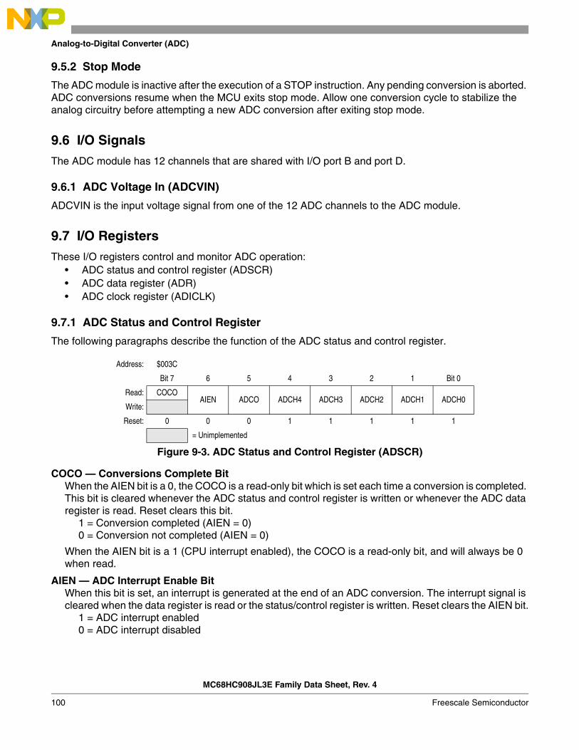
Analog-to-Digital Converter (ADC)
9.5.2 Stop Mode
The ADC module is inactive after the execution of a STOP instruction. Any pending conversion is aborted. ADC conversions resume when the MCU exits stop mode. Allow one conversion cycle to stabilize the analog circuitry before attempting a new ADC conversion after exiting stop mode.
9.6 I/O Signals
The ADC module has 12 channels that are shared with I/O port B and port D.
9.6.1 ADC Voltage In (ADCVIN)
ADCVIN is the input voltage signal from one of the 12 ADC channels to the ADC module.
9.7 I/O Registers
These I/O registers control and monitor ADC operation:• ADC status and control register (ADSCR)• ADC data register (ADR)• ADC clock register (ADICLK)
9.7.1 ADC Status and Control Register
The following paragraphs describe the function of the ADC status and control register.
COCO — Conversions Complete BitWhen the AIEN bit is a 0, the COCO is a read-only bit which is set each time a conversion is completed. This bit is cleared whenever the ADC status and control register is written or whenever the ADC data register is read. Reset clears this bit.
1 = Conversion completed (AIEN = 0) 0 = Conversion not completed (AIEN = 0)
When the AIEN bit is a 1 (CPU interrupt enabled), the COCO is a read-only bit, and will always be 0 when read.
AIEN — ADC Interrupt Enable BitWhen this bit is set, an interrupt is generated at the end of an ADC conversion. The interrupt signal is cleared when the data register is read or the status/control register is written. Reset clears the AIEN bit.
1 = ADC interrupt enabled0 = ADC interrupt disabled
Address: $003C
Bit 7 6 5 4 3 2 1 Bit 0
Read: COCOAIEN ADCO ADCH4 ADCH3 ADCH2 ADCH1 ADCH0
Write:
Reset: 0 0 0 1 1 1 1 1
= Unimplemented
Figure 9-3. ADC Status and Control Register (ADSCR)
MC68HC908JL3E Family Data Sheet, Rev. 4
100 Freescale Semiconductor

I/O Registers
ADCO — ADC Continuous Conversion BitWhen set, the ADC will convert samples continuously and update the ADR register at the end of each conversion. Only one conversion is allowed when this bit is cleared. Reset clears the ADCO bit.
1 = Continuous ADC conversion0 = One ADC conversion
ADCH[4:0] — ADC Channel Select BitsADCH[4:0] form a 5-bit field which is used to select one of the ADC channels. The five channel select bits are detailed in the following table. Care should be taken when using a port pin as both an analog and a digital input simultaneously to prevent switching noise from corrupting the analog signal.The ADC subsystem is turned off when the channel select bits are all set to one. This feature allows for reduced power consumption for the MCU when the ADC is not used. Reset sets all of these bits to a 1.
NOTERecovery from the disabled state requires one conversion cycle to stabilize.
Table 9-1. MUX Channel Select
ADCH4 ADCH3 ADCH2 ADCH1 ADCH0 ADC Channel Input Select
0 0 0 0 0 ADC0 PTB0
0 0 0 0 1 ADC1 PTB1
0 0 0 1 0 ADC2 PTB2
0 0 0 1 1 ADC3 PTB3
0 0 1 0 0 ADC4 PTB4
0 0 1 0 1 ADC5 PTB5
0 0 1 1 0 ADC6 PTB6
0 0 1 1 1 ADC7 PTB7
0 1 0 0 0 ADC8 PTD3
0 1 0 0 1 ADC9 PTD2
0 1 0 1 0 ADC10 PTD1
0 1 0 1 1 ADC11 PTD0
0 1 1 0 0Unused
(see Note 1): : : : : —
1 1 0 1 0
1 1 0 1 1 — Reserved
1 1 1 0 0 — Unused
1 1 1 0 1VDDA
(see Note 2)
1 1 1 1 0VSSA
(see Note 2)
1 1 1 1 1 ADC power off
1. If any unused channels are selected, the resulting ADC conversion will be unknown.2. The voltage levels supplied from internal reference nodes as specified in the table are used to verify the
operation of the ADC converter both in production test and for user applications.
MC68HC908JL3E Family Data Sheet, Rev. 4
Freescale Semiconductor 101

Analog-to-Digital Converter (ADC)
9.7.2 ADC Data Register
One 8-bit result register is provided. This register is updated each time an ADC conversion completes.
9.7.3 ADC Input Clock Register
This register selects the clock frequency for the ADC
ADIV[2:0] — ADC Clock Prescaler BitsADIV[2:0] form a 3-bit field which selects the divide ratio used by the ADC to generate the internal ADC clock. Table 9-2 shows the available clock configurations. The ADC clock should be set to approximately 1MHz.
Address: $003D
Bit 7 6 5 4 3 2 1 Bit 0
Read: AD7 AD6 AD5 AD4 AD3 AD2 AD1 AD0
Write:
Reset: Indeterminate after reset
= Unimplemented
Figure 9-4. ADC Data Register (ADR)
Address: $003E
Bit 7 6 5 4 3 2 1 Bit 0
Read:ADIV2 ADIV1 ADIV0
0 0 0 0 0
Write:
Reset: 0 0 0 0 0 0 0 0
= Unimplemented
Figure 9-5. ADC Input Clock Register (ADICLK)
Table 9-2. ADC Clock Divide Ratio
ADIV2 ADIV1 ADIV0 ADC Clock Rate
0 0 0 ADC Input Clock ÷ 1
0 0 1 ADC Input Clock ÷ 2
0 1 0 ADC Input Clock ÷ 4
0 1 1 ADC Input Clock ÷ 8
1 X X ADC Input Clock ÷ 16
X = don’t care
MC68HC908JL3E Family Data Sheet, Rev. 4
102 Freescale Semiconductor

Chapter 10 Input/Output (I/O) Ports
10.1 Introduction
Twenty three (23) bidirectional input-output (I/O) pins form three parallel ports. All I/O pins are programmable as inputs or outputs.
NOTEConnect any unused I/O pins to an appropriate logic level, either VDD or VSS. Although the I/O ports do not require termination for proper operation, termination reduces excess current consumption and the possibility of electrostatic damage.
20-pin devices have non-bonded pins. These pins should be configured either as outputs driving low or high, or as inputs with internal pullups enabled. Configuring these non-bonded pins in this manner will prrevent any excess current compsumption caused by floating inputs.
Addr. Register Name Bit 7 6 5 4 3 2 1 Bit 0
$0000Port A Data Register
(PTA)
Read: 0PTA6 PTA5 PTA4 PTA3 PTA2 PTA1 PTA0
Write:
Reset: Unaffected by reset
$0001Port B Data Register
(PTB)
Read:PTB7 PTB6 PTB5 PTB4 PTB3 PTB2 PTB1 PTB0
Write:
Reset: Unaffected by reset
$0003Port D Data Register
(PTD)
Read:PTD7 PTD6 PTD5 PTD4 PTD3 PTD2 PTD1 PTD0
Write:
Reset: Unaffected by reset
$0004Data Direction Register A
(DDRA)
Read: 0DDRA6 DDRA5 DDRA4 DDRA3 DDRA2 DDRA1 DDRA0
Write:
Reset: 0 0 0 0 0 0 0 0
$0005Data Direction Register B
(DDRB)
Read:DDRB7 DDRB6 DDRB5 DDRB4 DDRB3 DDRB2 DDRB1 DDRB0
Write:
Reset: 0 0 0 0 0 0 0 0
$0007Data Direction Register D
(DDRD)
Read:DDRD7 DDRD6 DDRD5 DDRD4 DDRD3 DDRD2 DDRD1 DDRD0
Write:
Reset: 0 0 0 0 0 0 0 0
Figure 10-1. I/O Port Register Summary
MC68HC908JL3E Family Data Sheet, Rev. 4
Freescale Semiconductor 103

Input/Output (I/O) Ports
$000APort D Control Register
(PDCR)
Read: 0 0 0 0SLOWD7 SLOWD6 PTDPU7 PTDPU6
Write:
Reset: 0 0 0 0 0 0 0 0
$000DPort A Input Pull-up Enable
Register(PTAPUE)
Read:PTA6EN PTAPUE6 PTAPUE5 PTAPUE4 PTAPUE3 PTAPUE2 PTAPUE1 PTAPUE0
Write:
Reset: 0 0 0 0 0 0 0 0
= Unimplemented
Table 10-1. Port Control Register Bits Summary
Port Bit DDRModule Control
PinModule Register Control Bit
A
0 DDRA0
KBI KBIER ($001B)
KBIE0 PTA0/KBI0
1 DDRA1 KBIE1 PTA1/KBI1
2 DDRA2 KBIE2 PTA2/KBI2
3 DDRA3 KBIE3 PTA3/KBI3
4 DDRA4 KBIE4 PTA4/KBI4
5 DDRA5 KBIE5 PTA5/KBI5
6 DDRA6OSCKBI
PTAPUE ($000D)KBIER ($001B)
PTA6ENKBIE6
RCCLK/PTA6/KBI6(1)
1. RCCLK/PTA6/KBI6 pin is only available on MC68HRC908JL3E/JK3E/JK1E devices (RC option); PTAPUE register has priority control over the port pin.RCCLK/PTA6/KBI6 is the OSC2 pin on MC68HC908JL3E/JK3E/JK1E devices (X-TAL option).
B
0 DDRB0
ADC ADSCR ($003C) ADCH[4:0]
PTB0/ADC0
1 DDRB1 PTB1/ADC1
2 DDRB2 PTB2/ADC2
3 DDRB3 PTB3/ADC3
4 DDRB4 PTB4/ADC4
5 DDRB5 PTB5/ADC5
6 DDRB6 PTB6/ADC6
7 DDRB7 PTB7/ADC7
D
0 DDRD0
ADC ADSCR ($003C) ADCH[4:0]
PTD0/ADC11
1 DDRD1 PTD1/ADC10
2 DDRD2 PTD2/ADC9
3 DDRD3 PTD3/ADC8
4 DDRD4TIM
TSC0 ($0025) ELS0B:ELS0A PTD4/TCH0
5 DDRD5 TSC1 ($0028) ELS1B:ELS1A PTD5/TCH1
6 DDRD6 — — — PTD6
7 DDRD7 — — — PTD7
Addr. Register Name Bit 7 6 5 4 3 2 1 Bit 0
Figure 10-1. I/O Port Register Summary
MC68HC908JL3E Family Data Sheet, Rev. 4
104 Freescale Semiconductor

Port A
10.2 Port A
Port A is an 7-bit special function port that shares all seven of its pins with the keyboard interrupt (KBI) module (see Chapter 12 Keyboard Interrupt Module (KBI)). Each port A pin also has software configurable pull-up device if the corresponding port pin is configured as input port. PTA0 to PTA5 has direct LED drive capability.
NOTEPTA0–PTA5 pins are available on MC68H(R)C908JL3E only.PTA6 pin is available on MC68HRC908JL3E/JK3E/JK1E only.
10.2.1 Port A Data Register (PTA)
The port A data register (PTA) contains a data latch for each of the seven port A pins.
PTA[6:0] — Port A Data BitsThese read/write bits are software programmable. Data direction of each port A pin is under the control of the corresponding bit in data direction register A. Reset has no effect on port A data.
KBI[6:0] — Port A Keyboard InterruptsThe keyboard interrupt enable bits, KBIE[6:0], in the keyboard interrupt control register (KBIER) enable the port A pins as external interrupt pins, (see Chapter 12 Keyboard Interrupt Module (KBI)).
Address: $0000
Bit 7 6 5 4 3 2 1 Bit 0
Read: 0PTA6 PTA5 PTA4 PTA3 PTA2 PTA1 PTA0
Write:
Reset: Unaffected by Reset
Additional Functions:LED
(Sink)LED
(Sink)LED
(Sink)LED
(Sink)LED
(Sink)LED
(Sink)
30k pull-up 30k pull-up 30k pull-up 30k pull-up 30k pull-up 30k pull-up 30k pull-up
Keyboard Interrupt
Keyboard Interrupt
Keyboard Interrupt
Keyboard Interrupt
Keyboard Interrupt
Keyboard Interrupt
Keyboard Interrupt
= Unimplemented
Figure 10-2. Port A Data Register (PTA)
MC68HC908JL3E Family Data Sheet, Rev. 4
Freescale Semiconductor 105

Input/Output (I/O) Ports
10.2.2 Data Direction Register A (DDRA)
Data direction register A determines whether each port A pin is an input or an output. Writing a one to a DDRA bit enables the output buffer for the corresponding port A pin; a zero disables the output buffer.
DDRA[6:0] — Data Direction Register A BitsThese read/write bits control port A data direction. Reset clears DDRA[6:0], configuring all port A pins as inputs.
1 = Corresponding port A pin configured as output0 = Corresponding port A pin configured as input
NOTEAvoid glitches on port A pins by writing to the port A data register before changing data direction register A bits from 0 to 1.
Figure 10-4 shows the port A I/O logic.
Figure 10-4. Port A I/O Circuit
When DDRAx is a 1, reading address $0000 reads the PTAx data latch. When DDRAx is a 0, reading address $0000 reads the voltage level on the pin. The data latch can always be written, regardless of the state of its data direction bit.
Address: $0004
Bit 7 6 5 4 3 2 1 Bit 0
Read: 0DDRA6 DDRA5 DDRA4 DDRA3 DDRA2 DDRA1 DDRA0
Write:
Reset: 0 0 0 0 0 0 0 0
= Unimplemented
Figure 10-3. Data Direction Register A (DDRA)
READ DDRA ($0004)
WRITE DDRA ($0004)
RESET
WRITE PTA ($0000)
READ PTA ($0000)
PTAx
DDRAx
PTAx
INTE
RN
AL D
ATA
BUS
30k
PTAPUEx
To Keyboard Interrupt Circuit
MC68HC908JL3E Family Data Sheet, Rev. 4
106 Freescale Semiconductor

Port A
10.2.3 Port A Input Pull-up Enable Register (PTAPUE)
The port A input pull-up enable register (PTAPUE) contains a software configurable pull-up device for each of the seven port A pins. Each bit is individually configurable and requires the corresponding data direction register, DDRAx be configured as input. Each pull-up device is automatically and dynamically disabled when its corresponding DDRAx bit is configured as output.
PTA6EN — Enable PTA6 on OSC2This read/write bit configures the OSC2 pin function when RC oscillator option is selected. This bit has no effect for X-tal oscillator option.
1 = OSC2 pin configured for PTA6 I/O, and has all the interrupt and pull-up functions0 = OSC2 pin outputs the RC oscillator clock (RCCLK)
PTAPUE[6:0] — Port A Input Pull-up Enable BitsThese read/write bits are software programmable to enable pull-up devices on port A pins
1 = Corresponding port A pin configured to have internal pull-up if its DDRA bit is set to 00 = Pull-up device is disconnected on the corresponding port A pin regardless of the state of its
DDRA bit
Table 10-2 summarizes the operation of the port A pins.
Address: $000D
Bit 7 6 5 4 3 2 1 Bit 0
Read:PTA6EN PTAPUE6 PTAPUE5 PTAPUE4 PTAPUE3 PTAPUE2 PTAPUE1 PTAPUE0
Write:
Reset: 0 0 0 0 0 0 0 0
Figure 10-5. Port A Input Pull-up Enable Register (PTAPUE)
Table 10-2. Port A Pin Functions
PTAPUE BitDDRA
BitPTA Bit I/O Pin Mode
Accesses to DDRA Accesses to PTA
Read/Write Read Write
1 0 X(1)
1. X = Don’t care.
Input, VDD(2)
2. I/O pin pulled to VDD by internal pull-up.
DDRA[6:0] Pin PTA[6:0](3)
3. Writing affects data register, but does not affect input.
0 0 X Input, Hi-Z(4)
4. Hi-Z = High Impedance.
DDRA[6:0] Pin PTA[6:0](3)
X 1 X Output DDRA[6:0] PTA[6:0] PTA[6:0]
MC68HC908JL3E Family Data Sheet, Rev. 4
Freescale Semiconductor 107
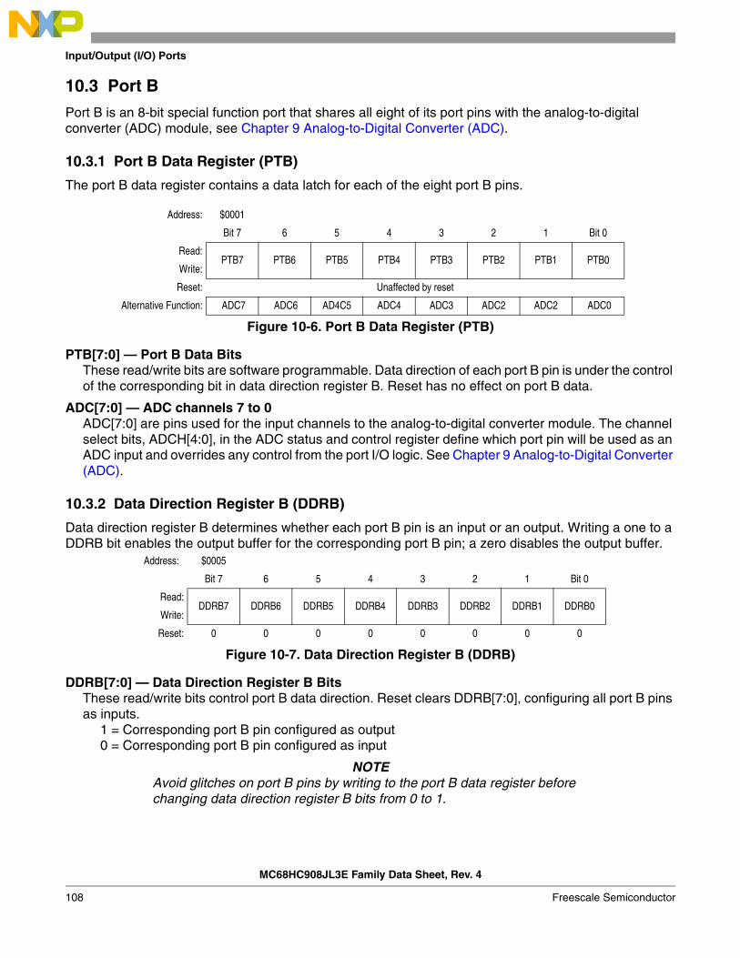
Input/Output (I/O) Ports
10.3 Port B
Port B is an 8-bit special function port that shares all eight of its port pins with the analog-to-digital converter (ADC) module, see Chapter 9 Analog-to-Digital Converter (ADC).
10.3.1 Port B Data Register (PTB)
The port B data register contains a data latch for each of the eight port B pins.
PTB[7:0] — Port B Data BitsThese read/write bits are software programmable. Data direction of each port B pin is under the control of the corresponding bit in data direction register B. Reset has no effect on port B data.
ADC[7:0] — ADC channels 7 to 0ADC[7:0] are pins used for the input channels to the analog-to-digital converter module. The channel select bits, ADCH[4:0], in the ADC status and control register define which port pin will be used as an ADC input and overrides any control from the port I/O logic. See Chapter 9 Analog-to-Digital Converter (ADC).
10.3.2 Data Direction Register B (DDRB)
Data direction register B determines whether each port B pin is an input or an output. Writing a one to a DDRB bit enables the output buffer for the corresponding port B pin; a zero disables the output buffer.
DDRB[7:0] — Data Direction Register B BitsThese read/write bits control port B data direction. Reset clears DDRB[7:0], configuring all port B pins as inputs.
1 = Corresponding port B pin configured as output0 = Corresponding port B pin configured as input
NOTEAvoid glitches on port B pins by writing to the port B data register before changing data direction register B bits from 0 to 1.
Address: $0001
Bit 7 6 5 4 3 2 1 Bit 0
Read:PTB7 PTB6 PTB5 PTB4 PTB3 PTB2 PTB1 PTB0
Write:
Reset: Unaffected by reset
Alternative Function: ADC7 ADC6 AD4C5 ADC4 ADC3 ADC2 ADC2 ADC0
Figure 10-6. Port B Data Register (PTB)
Address: $0005
Bit 7 6 5 4 3 2 1 Bit 0
Read:DDRB7 DDRB6 DDRB5 DDRB4 DDRB3 DDRB2 DDRB1 DDRB0
Write:
Reset: 0 0 0 0 0 0 0 0
Figure 10-7. Data Direction Register B (DDRB)
MC68HC908JL3E Family Data Sheet, Rev. 4
108 Freescale Semiconductor

Port B
Figure 10-8. Port B I/O Circuit
When DDRBx is a 1, reading address $0001 reads the PTBx data latch. When DDRBx is a 0, reading address $0001 reads the voltage level on the pin. The data latch can always be written, regardless of the state of its data direction bit. Table 10-3 summarizes the operation of the port B pins.
Table 10-3. Port B Pin Functions
DDRB Bit PTB Bit I/O Pin ModeAccesses to DDRB Accesses to PTB
Read/Write Read Write
0 X(1)
1. X = don’t care.
Input, Hi-Z(2)
2. Hi-Z = high impedance.
DDRB[7:0] Pin PTB[7:0](3)
3. Writing affects data register, but does not affect the input.
1 X Output DDRB[7:0] Pin PTB[7:0]
READ DDRB ($0005)
WRITE DDRB ($0005)
RESET
WRITE PTB ($0001)
READ PTB ($0001)
PTBx
DDRBx
PTBx
INTE
RN
AL D
ATA
BUS
To Analog-To-Digital Converter
MC68HC908JL3E Family Data Sheet, Rev. 4
Freescale Semiconductor 109

Input/Output (I/O) Ports
10.4 Port D
Port D is an 8-bit special function port that shares two of its pins with timer interface module, (see Chapter 8 Timer Interface Module (TIM)) and shares four of its pins with analog-to-digital converter module (see Chapter 9 Analog-to-Digital Converter (ADC)). PTD6 and PTD7 each has high current drive (25mA sink) and programmable pull-up. PTD2, PTD3, PTD6 and PTD7 each has LED driving (sink) capability.
NOTEPTD0–PTD1 are available on MC68H(R)C908JL3E only.
10.4.1 Port D Data Register (PTD)
The port D data register contains a data latch for each of the eight port D pins.
PTD[7:0] — Port D Data BitsThese read/write bits are software programmable. Data direction of each port D pin is under the control of the corresponding bit in data direction register D. Reset has no effect on port D data.
ADC[11:8] — ADC channels 11 to 8ADC[11:8] are pins used for the input channels to the analog-to-digital converter module. The channel select bits, ADCH[4:0], in the ADC status and control register define which port pin will be used as an ADC input and overrides any control from the port I/O logic. See Chapter 9 Analog-to-Digital Converter (ADC).
TCH[1:0] — Timer Channel I/OThe TCH1 and TCH0 pins are the TIM input capture/output compare pins. The edge/level select bits, ELSxB:ELSxA, determine whether the PTD4/TCH0 and PTD5/TCH1 pins are timer channel I/O pins or general-purpose I/O pins. See Chapter 8 Timer Interface Module (TIM).
Address: $0003
Bit 7 6 5 4 3 2 1 Bit 0
Read:PTD7 PTD6 PTD5 PTD4 PTD3 PTD2 PTD1 PTD0
Write:
Reset: Unaffected by reset
Additional Functions: LED(Sink)
LED(Sink)
LED(Sink)
LED(Sink)
ADC8 ADC9 ADC10 ADC11
TCH1 TCH0
25mA sink(Slow Edge)
25mA sink(Slow Edge)
5k pull-up 5k pull-up
= Unimplemented
Figure 10-9. Port D Data Register (PTD)
MC68HC908JL3E Family Data Sheet, Rev. 4
110 Freescale Semiconductor

Port D
10.4.2 Data Direction Register D (DDRD)
Data direction register D determines whether each port D pin is an input or an output. Writing a one to a DDRD bit enables the output buffer for the corresponding port D pin; a zero disables the output buffer.
DDRD[7:0] — Data Direction Register D BitsThese read/write bits control port D data direction. Reset clears DDRD[7:0], configuring all port D pins as inputs.
1 = Corresponding port D pin configured as output0 = Corresponding port D pin configured as input
NOTEAvoid glitches on port D pins by writing to the port D data register before changing data direction register D bits from 0 to 1. Figure 10-11 shows the port D I/O logic.
Figure 10-11. Port D I/O Circuit
When DDRDx is a 1, reading address $0003 reads the PTDx data latch. When DDRDx is a 0, reading address $0003 reads the voltage level on the pin. The data latch can always be written, regardless of the state of its data direction bit. Table 10-4 summarizes the operation of the port D pins.
Address: $0007
Bit 7 6 5 4 3 2 1 Bit 0
Read:DDRD7 DDRD6 DDRD5 DDRD4 DDRD3 DDRD2 DDRD1 DDRD0
Write:
Reset: 0 0 0 0 0 0 0 0
Figure 10-10. Data Direction Register D (DDRD)
READ DDRD ($0007)
WRITE DDRD ($0007)
RESET
WRITE PTD ($0003)
READ PTD ($0003)
PTDx
DDRDx
PTDx
INTE
RN
AL D
ATA
BUS
PTD[0:3] To Analog-To-Digital Converter
5k
PTDPU[6:7]
PTD[4:5] To Timer
MC68HC908JL3E Family Data Sheet, Rev. 4
Freescale Semiconductor 111

Input/Output (I/O) Ports
10.4.3 Port D Control Register (PDCR)
The port D control register enables/disables the pull-up resistor and slow-edge high current capability of pins PTD6 and PTD7.
SLOWDx — Slow Edge EnableThe SLOWD6 and SLOWD7 bits enable the Slow-edge, open-drain, high current output (25mA sink) of port pins PTD6 and PTD7 respectively. DDRDx bit is not affected by SLOWDx.
1 = Slow edge enabled; pin is open-drain output0 = Slow edge disabled; pin is push-pull
PTDPUx — Pull-up EnableThe PTDPU6 and PTDPU7 bits enable the 5kΩ pull-up on PTD6 and PTD7 respectively, regardless the status of DDRDx bit.
1 = Enable 5kΩ pull-up0 = Disable 5kΩ pull-up
Table 10-4. Port D Pin Functions
DDRDBit
PTD Bit I/O Pin Mode
Accesses to DDRD
Accesses to PTD
Read/Write Read Write
0 X(1)
1. X = don’t care.
Input, Hi-Z(2)
2. Hi-Z = high impedance.
DDRD[7:0] Pin PTD[7:0](3)
3. Writing affects data register, but does not affect the input.
1 X Output DDRD[7:0] Pin PTD[7:0]
Address: $000A
Bit 7 6 5 4 3 2 1 Bit 0
Read: 0 0 0 0SLOWD7 SLOWD6 PTDPU7 PTDPU6
Write:
Reset: 0 0 0 0 0 0 0 0
= Unimplemented
Figure 10-12. Port D Control Register (PDCR)
MC68HC908JL3E Family Data Sheet, Rev. 4
112 Freescale Semiconductor

Chapter 11 External Interrupt (IRQ)
11.1 Introduction
The IRQ (external interrupt) module provides a maskable interrupt input.
11.2 Features
Features of the IRQ module include the following:• A dedicated external interrupt pin, IRQ• IRQ interrupt control bits• Hysteresis buffer• Programmable edge-only or edge and level interrupt sensitivity• Automatic interrupt acknowledge• Selectable internal pullup resistor
11.3 Functional Description
A logic zero applied to the external interrupt pin can latch a CPU interrupt request. Figure 11-1 shows the structure of the IRQ module.
Interrupt signals on the IRQ pin are latched into the IRQ latch. An interrupt latch remains set until one of the following actions occurs:
• Vector fetch — A vector fetch automatically generates an interrupt acknowledge signal that clears the IRQ latch.
• Software clear — Software can clear the interrupt latch by writing to the acknowledge bit in the interrupt status and control register (INTSCR). Writing a one to the ACK bit clears the IRQ latch.
• Reset — A reset automatically clears the interrupt latch.
The external interrupt pin is falling-edge-triggered and is software-configurable to be either falling-edge or falling-edge and low-level-triggered. The MODE bit in the INTSCR controls the triggering sensitivity of the IRQ pin.
When the interrupt pin is edge-triggered only, the CPU interrupt request remains set until a vector fetch, software clear, or reset occurs.
When the interrupt pin is both falling-edge and low-level-triggered, the CPU interrupt request remains set until both of the following occur:
• Vector fetch or software clear• Return of the interrupt pin to logic one
MC68HC908JL3E Family Data Sheet, Rev. 4
Freescale Semiconductor 113
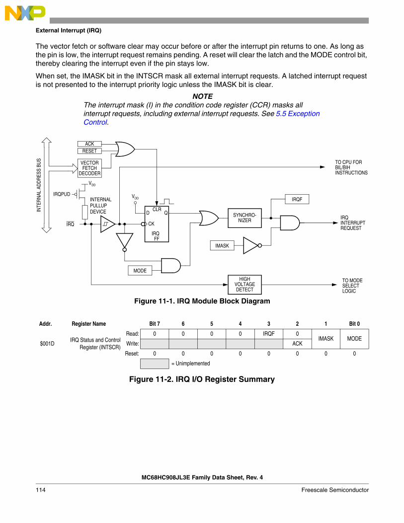
External Interrupt (IRQ)
The vector fetch or software clear may occur before or after the interrupt pin returns to one. As long as the pin is low, the interrupt request remains pending. A reset will clear the latch and the MODE control bit, thereby clearing the interrupt even if the pin stays low.
When set, the IMASK bit in the INTSCR mask all external interrupt requests. A latched interrupt request is not presented to the interrupt priority logic unless the IMASK bit is clear.
NOTEThe interrupt mask (I) in the condition code register (CCR) masks all interrupt requests, including external interrupt requests. See 5.5 Exception Control.
Figure 11-1. IRQ Module Block Diagram
Addr. Register Name Bit 7 6 5 4 3 2 1 Bit 0
$001DIRQ Status and Control
Register (INTSCR)
Read: 0 0 0 0 IRQF 0IMASK MODE
Write: ACK
Reset: 0 0 0 0 0 0 0 0
= Unimplemented
Figure 11-2. IRQ I/O Register Summary
ACK
IMASK
D Q
CK
CLR
IRQ
HIGH
INTERRUPT
TO MODESELECTLOGIC
IRQFF
REQUEST
VDD
MODE
VOLTAGEDETECT
SYNCHRO-NIZER
IRQF
TO CPU FORBIL/BIHINSTRUCTIONS
VECTORFETCH
DECODER
INTE
RN
AL A
DD
RES
S BU
S
RESET
VDD
IRQ
IRQPUDINTERNALPULLUPDEVICE
MC68HC908JL3E Family Data Sheet, Rev. 4
114 Freescale Semiconductor

IRQ Module During Break Interrupts
11.3.1 IRQ Pin
A zero on the IRQ pin can latch an interrupt request into the IRQ latch. A vector fetch, software clear, or reset clears the IRQ latch.
If the MODE bit is set, the IRQ pin is both falling-edge-sensitive and low-level-sensitive. With MODE set, both of the following actions must occur to clear IRQ:
• Vector fetch or software clear — A vector fetch generates an interrupt acknowledge signal to clear the latch. Software may generate the interrupt acknowledge signal by writing a logic one to the ACK bit in the interrupt status and control register (INTSCR). The ACK bit is useful in applications that poll the IRQ pin and require software to clear the IRQ latch. Writing to the ACK bit prior to leaving an interrupt service routine can also prevent spurious interrupts due to noise. Setting ACK does not affect subsequent transitions on the IRQ pin. A falling edge that occurs after writing to the ACK bit latches another interrupt request. If the IRQ mask bit, IMASK, is clear, the CPU loads the program counter with the vector address at locations $FFFA and $FFFB.
• Return of the IRQ pin to logic one — As long as the IRQ pin is at logic zero, IRQ remains active.
The vector fetch or software clear and the return of the IRQ pin to logic one may occur in any order. The interrupt request remains pending as long as the IRQ pin is at logic zero. A reset will clear the latch and the MODE control bit, thereby clearing the interrupt even if the pin stays low.
If the MODE bit is clear, the IRQ pin is falling-edge-sensitive only. With MODE clear, a vector fetch or software clear immediately clears the IRQ latch.
The IRQF bit in the INTSCR register can be used to check for pending interrupts. The IRQF bit is not affected by the IMASK bit, which makes it useful in applications where polling is preferred.
Use the BIH or BIL instruction to read the logic level on the IRQ pin.
NOTEWhen using the level-sensitive interrupt trigger, avoid false interrupts by masking interrupt requests in the interrupt routine.
NOTEAn internal pull-up resistor to VDD is connected to the IRQ pin; this can be disabled by setting the IRQPUD bit in the CONFIG2 register ($001E).
11.4 IRQ Module During Break Interrupts
The system integration module (SIM) controls whether the IRQ latch can be cleared during the break state. The BCFE bit in the break flag control register (BFCR) enables software to clear the latches during the break state. (See Chapter 5 System Integration Module (SIM).)
To allow software to clear the IRQ latch during a break interrupt, write a one to the BCFE bit. If a latch is cleared during the break state, it remains cleared when the MCU exits the break state.
To protect the latches during the break state, write a zero to the BCFE bit. With BCFE at zero (its default state), writing to the ACK bit in the IRQ status and control register during the break state has no effect on the IRQ latch.
MC68HC908JL3E Family Data Sheet, Rev. 4
Freescale Semiconductor 115

External Interrupt (IRQ)
11.5 IRQ Status and Control Register (INTSCR)
The IRQ status and control register (INTSCR) controls and monitors operation of the IRQ module. The INTSCR has the following functions:
• Shows the state of the IRQ flag• Clears the IRQ latch• Masks IRQ and interrupt request• Controls triggering sensitivity of the IRQ interrupt pin
IRQF — IRQ FlagThis read-only status bit is high when the IRQ interrupt is pending.
1 = IRQ interrupt pending0 = IRQ interrupt not pending
ACK — IRQ Interrupt Request Acknowledge BitWriting a one to this write-only bit clears the IRQ latch. ACK always reads as zero. Reset clears ACK.
IMASK — IRQ Interrupt Mask BitWriting a one to this read/write bit disables IRQ interrupt requests. Reset clears IMASK.
1 = IRQ interrupt requests disabled0 = IRQ interrupt requests enabled
MODE — IRQ Edge/Level Select BitThis read/write bit controls the triggering sensitivity of the IRQ pin. Reset clears MODE.
1 = IRQ interrupt requests on falling edges and low levels0 = IRQ interrupt requests on falling edges only
IRQPUD — IRQ Pin Pull-up control bit1 = Internal pull-up is disconnected0 = Internal pull-up is connected between IRQ pin and VDD
Address: $001D
Bit 7 6 5 4 3 2 1 Bit 0
Read: 0 0 0 0 IRQFIMASK MODE
Write: ACK
Reset: 0 0 0 0 0 0 0 0
= Unimplemented
Figure 11-3. IRQ Status and Control Register (INTSCR)
Address: $001E
Bit 7 6 5 4 3 2 1 Bit 0
Read:IRQPUD R R LVIT1 LVIT0 R R R
Write:
Reset: 0 0 0 Not affected Not affected 0 0 0
POR: 0 0 0 0 0 0 0 0
R = Reserved
Figure 11-4. Configuration Register 2 (CONFIG2)
MC68HC908JL3E Family Data Sheet, Rev. 4
116 Freescale Semiconductor

Chapter 12 Keyboard Interrupt Module (KBI)
12.1 Introduction
The keyboard interrupt module (KBI) provides seven independently maskable external interrupts which are accessible via PTA0–PTA6 pins.
12.2 Features
Features of the keyboard interrupt module include the following:• Seven keyboard interrupt pins with separate keyboard interrupt enable bits and one keyboard
interrupt mask• Software configurable pull-up device if input pin is configured as input port bit• Programmable edge-only or edge- and level- interrupt sensitivity• Exit from low-power modes
12.3 I/O Pins
The seven keyboard interrupt pins are shared with standard port I/O pins. The full name of the KBI pins are listed in Table 12-1. The generic pin name appear in the text that follows.
Addr. Register Name Bit 7 6 5 4 3 2 1 Bit 0
$001AKeyboard Status and Control
Register (KBSCR)
Read: 0 0 0 0 KEYF 0IMASKK MODEK
Write: ACKK
Reset: 0 0 0 0 0 0 0 0
$001BKeyboard Interrupt Enable
Register (KBIER)
Read: 0KBIE6 KBIE5 KBIE4 KBIE3 KBIE2 KBIE1 KBIE0
Write:
Reset: 0 0 0 0 0 0 0 0
= Unimplemented
Figure 12-1. KBI I/O Register Summary
Table 12-1. Pin Name Conventions
KBIGeneric Pin Name
Full MCU Pin NamePin Selected for KBI Function
by KBIEx Bit in KBIER
KBI0–KBI5 PTA0/KBI0–PTA5/KBI5 KBIE0–KBIE5
KBI6 RCCLK/PTA6/KBI6(1)
1. RCCLK/PTA6/KBI6 pin is only available on MC68HRC908JL3E/JK3E/JK1E devices (RC option).
KBIE6
MC68HC908JL3E Family Data Sheet, Rev. 4
Freescale Semiconductor 117

Keyboard Interrupt Module (KBI)
12.4 Functional Description
Figure 12-2. Keyboard Interrupt Block Diagram
Writing to the KBIE6–KBIE0 bits in the keyboard interrupt enable register independently enables or disables each port A pin as a keyboard interrupt pin. Enabling a keyboard interrupt pin in port A also enables its internal pull-up device irrespective of PTAPUEx bits in the port A input pull-up enable register (see 10.2.3 Port A Input Pull-up Enable Register (PTAPUE)). A logic 0 applied to an enabled keyboard interrupt pin latches a keyboard interrupt request.
A keyboard interrupt is latched when one or more keyboard pins goes low after all were high. The MODEK bit in the keyboard status and control register controls the triggering mode of the keyboard interrupt.
• If the keyboard interrupt is edge-sensitive only, a falling edge on a keyboard pin does not latch an interrupt request if another keyboard pin is already low. To prevent losing an interrupt request on one pin because another pin is still low, software can disable the latter pin while it is low.
• If the keyboard interrupt is falling edge- and low level-sensitive, an interrupt request is present as long as any keyboard pin is low.
If the MODEK bit is set, the keyboard interrupt pins are both falling edge- and low level-sensitive, and both of the following actions must occur to clear a keyboard interrupt request:
• Vector fetch or software clear — A vector fetch generates an interrupt acknowledge signal to clear the interrupt request. Software may generate the interrupt acknowledge signal by writing a 1 to the ACKK bit in the keyboard status and control register KBSCR. The ACKK bit is useful in applications that poll the keyboard interrupt pins and require software to clear the keyboard interrupt request. Writing to the ACKK bit prior to leaving an interrupt service routine can also prevent spurious interrupts due to noise. Setting ACKK does not affect subsequent transitions on the keyboard interrupt pins. A falling edge that occurs after writing to the ACKK bit latches another interrupt request. If the keyboard interrupt mask bit, IMASKK, is clear, the CPU loads the program counter with the vector address at locations $FFE0 and $FFE1.
• Return of all enabled keyboard interrupt pins to logic 1 — As long as any enabled keyboard interrupt pin is at 0, the keyboard interrupt remains set.
KBIE0
KBIE6
.
.
.
D Q
CK
CLR
VDD
MODEK
IMASKKKEYBOARDINTERRUPT FF
VECTOR FETCHDECODERACKK
INTERNAL BUS
RESET
KBI6
KBI0
SYNCHRONIZER
KEYF
TO PULLUP ENABLE
TO PULLUP ENABLE
KEYBOARDINTERRUPTREQUEST
MC68HC908JL3E Family Data Sheet, Rev. 4
118 Freescale Semiconductor

Keyboard Interrupt Registers
The vector fetch or software clear and the return of all enabled keyboard interrupt pins to 1 may occur in any order.
If the MODEK bit is clear, the keyboard interrupt pin is falling-edge-sensitive only. With MODEK clear, a vector fetch or software clear immediately clears the keyboard interrupt request.
Reset clears the keyboard interrupt request and the MODEK bit, clearing the interrupt request even if a keyboard interrupt pin stays at 0.
The keyboard flag bit (KEYF) in the keyboard status and control register can be used to see if a pending interrupt exists. The KEYF bit is not affected by the keyboard interrupt mask bit (IMASKK) which makes it useful in applications where polling is preferred.
To determine the logic level on a keyboard interrupt pin, disable the pull-up device, use the data direction register to configure the pin as an input and then read the data register.
NOTESetting a keyboard interrupt enable bit (KBIEx) forces the corresponding keyboard interrupt pin to be an input, overriding the data direction register. However, the data direction register bit must be a 0 for software to read the pin.
12.4.1 Keyboard Initialization
When a keyboard interrupt pin is enabled, it takes time for the internal pull-up to reach a logic 1. Therefore a false interrupt can occur as soon as the pin is enabled.
To prevent a false interrupt on keyboard initialization:1. Mask keyboard interrupts by setting the IMASKK bit in the keyboard status and control register.2. Enable the KBI pins by setting the appropriate KBIEx bits in the keyboard interrupt enable register.3. Write to the ACKK bit in the keyboard status and control register to clear any false interrupts.4. Clear the IMASKK bit.
An interrupt signal on an edge-triggered pin can be acknowledged immediately after enabling the pin. An interrupt signal on an edge- and level-triggered interrupt pin must be acknowledged after a delay that depends on the external load.
Another way to avoid a false interrupt:1. Configure the keyboard pins as outputs by setting the appropriate DDRA bits in the data direction
register A.2. Write 1s to the appropriate port A data register bits.3. Enable the KBI pins by setting the appropriate KBIEx bits in the keyboard interrupt enable register.
12.5 Keyboard Interrupt Registers
Two registers control the operation of the keyboard interrupt module:• Keyboard status and control register• Keyboard interrupt enable register
MC68HC908JL3E Family Data Sheet, Rev. 4
Freescale Semiconductor 119

Keyboard Interrupt Module (KBI)
12.5.1 Keyboard Status and Control Register• Flags keyboard interrupt requests• Acknowledges keyboard interrupt requests• Masks keyboard interrupt requests• Controls keyboard interrupt triggering sensitivity
KEYF — Keyboard Flag BitThis read-only bit is set when a keyboard interrupt is pending on port-A. Reset clears the KEYF bit.
1 = Keyboard interrupt pending0 = No keyboard interrupt pending
ACKK — Keyboard Acknowledge BitWriting a 1 to this write-only bit clears the keyboard interrupt request on port-A. ACKK always reads as 0. Reset clears ACKK.
IMASKK— Keyboard Interrupt Mask BitWriting a 1 to this read/write bit prevents the output of the keyboard interrupt mask from generating interrupt requests on port-A. Reset clears the IMASKK bit.
1 = Keyboard interrupt requests masked0 = Keyboard interrupt requests not masked
MODEK — Keyboard Triggering Sensitivity BitThis read/write bit controls the triggering sensitivity of the keyboard interrupt pins on port-A. Reset clears MODEK.
1 = Keyboard interrupt requests on falling edges and low levels0 = Keyboard interrupt requests on falling edges only
Address: $001A
Bit 7 6 5 4 3 2 1 Bit 0
Read: 0 0 0 0 KEYF 0IMASKK MODEK
Write: ACKK
Reset: 0 0 0 0 0 0 0 0
= Unimplemented
Figure 12-3. Keyboard Status and Control Register (KBSCR)
MC68HC908JL3E Family Data Sheet, Rev. 4
120 Freescale Semiconductor

Low-Power Modes
12.5.2 Keyboard Interrupt Enable Register
The port-A keyboard interrupt enable register enables or disables each port-A pin to operate as a keyboard interrupt pin.
KBIE6–KBIE0 — Port-A Keyboard Interrupt Enable BitsEach of these read/write bits enables the corresponding keyboard interrupt pin on port-A to latch interrupt requests. Reset clears the keyboard interrupt enable register.
1 = KBIx pin enabled as keyboard interrupt pin0 = KBIx pin not enabled as keyboard interrupt pin
12.6 Low-Power Modes
The WAIT and STOP instructions put the MCU in low power-consumption standby modes.
12.6.1 Wait Mode
The keyboard modules remain active in wait mode. Clearing the IMASKK bit in the keyboard status and control register enables keyboard interrupt requests to bring the MCU out of wait mode.
12.6.2 Stop Mode
The keyboard module remains active in stop mode. Clearing the IMASKK bit in the keyboard status and control register enables keyboard interrupt requests to bring the MCU out of stop mode.
12.7 Keyboard Module During Break Interrupts
The system integration module (SIM) controls whether the keyboard interrupt latch can be cleared during the break state. The BCFE bit in the break flag control register (BFCR) enables software to clear status bits during the break state.
To allow software to clear the keyboard interrupt latch during a break interrupt, write a 1 to the BCFE bit. If a latch is cleared during the break state, it remains cleared when the MCU exits the break state.
To protect the latch during the break state, write a 0 to the BCFE bit. With BCFE at 0 (its default state), writing to the keyboard acknowledge bit (ACKK) in the keyboard status and control register during the break state has no effect.
Address: $001B
Bit 7 6 5 4 3 2 1 Bit 0
Read: 0KBIE6 KBIE5 KBIE4 KBIE3 KBIE2 KBIE1 KBIE0
Write:
Reset: 0 0 0 0 0 0 0 0
= Unimplemented
Figure 12-4. Keyboard Interrupt Enable Register (KBIER)
MC68HC908JL3E Family Data Sheet, Rev. 4
Freescale Semiconductor 121

Keyboard Interrupt Module (KBI)
MC68HC908JL3E Family Data Sheet, Rev. 4
122 Freescale Semiconductor

Chapter 13 Computer Operating Properly (COP)
13.1 Introduction
The computer operating properly (COP) module contains a free-running counter that generates a reset if allowed to overflow. The COP module helps software recover from runaway code. Prevent a COP reset by clearing the COP counter periodically. The COP module can be disabled through the COPD bit in the CONFIG1 register.
13.2 Functional Description
Figure 13-1 shows the structure of the COP module.
Figure 13-1. COP Block Diagram
COPCTL WRITE
2OSCOUT
RESET VECTOR FETCH
SIM RESET CIRCUIT
RESET STATUS REGISTER
INTERNAL RESET SOURCES(1)
SIM
CLEA
R ST
AGES
5–1
2
12-BIT SIM COUNTER
CLEA
R AL
L ST
AGES
COPD (FROM CONFIG1)
RESET
COPCTL WRITECLEAR
COP MODULE
COPEN (FROM SIM)
COP COUNTER
NOTE: See Chapter 5 System Integration Module (SIM) for more details.
COP CLOCK
COP
TIM
EOUT
COP RATE SEL (COPRS FROM CONFIG1)
6-BIT COP COUNTER
MC68HC908JL3E Family Data Sheet, Rev. 4
Freescale Semiconductor 123

Computer Operating Properly (COP)
The COP counter is a free-running 6-bit counter preceded by the 12-bit system integration module (SIM) counter. If not cleared by software, the COP counter overflows and generates an asynchronous reset after 262,128 or 8176 2OSCOUT cycles; depending on the state of the COP rate select bit, COPRS, in configuration register 1. With a 262,128 2OSCOUT cycle overflow option, a 8MHz crystal gives a COP timeout period of 32.766 ms. Writing any value to location $FFFF before an overflow occurs prevents a COP reset by clearing the COP counter and stages 12 through 5 of the SIM counter.
NOTEService the COP immediately after reset and before entering or after exiting stop mode to guarantee the maximum time before the first COP counter overflow.
A COP reset pulls the RST pin low for 32 × 2OSCOUT cycles and sets the COP bit in the reset status register (RSR). (See 5.7.2 Reset Status Register (RSR).).
NOTEPlace COP clearing instructions in the main program and not in an interrupt subroutine. Such an interrupt subroutine could keep the COP from generating a reset even while the main program is not working properly.
13.3 I/O Signals
The following paragraphs describe the signals shown in Figure 13-1.
13.3.1 2OSCOUT
2OSCOUT is the oscillator output signal. 2OSCOUT frequency is equal to the crystal frequency or the RC-oscillator frequency.
13.3.2 COPCTL Write
Writing any value to the COP control register (COPCTL) (see 13.4 COP Control Register) clears the COP counter and clears bits 12 through 5 of the SIM counter. Reading the COP control register returns the low byte of the reset vector.
13.3.3 Power-On Reset
The power-on reset (POR) circuit in the SIM clears the SIM counter 4096 × 2OSCOUT cycles after power-up.
13.3.4 Internal Reset
An internal reset clears the SIM counter and the COP counter.
13.3.5 Reset Vector Fetch
A reset vector fetch occurs when the vector address appears on the data bus. A reset vector fetch clears the SIM counter.
13.3.6 COPD (COP Disable)
The COPD signal reflects the state of the COP disable bit (COPD) in the configuration register (CONFIG). (See Chapter 3 Configuration Registers (CONFIG).)
MC68HC908JL3E Family Data Sheet, Rev. 4
124 Freescale Semiconductor

COP Control Register
13.3.7 COPRS (COP Rate Select)
The COPRS signal reflects the state of the COP rate select bit (COPRS) in the configuration register 1.
COPRS — COP Rate Select BitCOPRS selects the COP timeout period. Reset clears COPRS.
1 = COP timeout period is 8176 × 2OSCOUT cycles0 = COP timeout period is 262,128 × 2OSCOUT cycles
COPD — COP Disable BitCOPD disables the COP module.
1 = COP module disabled0 = COP module enabled
13.4 COP Control Register
The COP control register is located at address $FFFF and overlaps the reset vector. Writing any value to $FFFF clears the COP counter and starts a new timeout period. Reading location $FFFF returns the low byte of the reset vector.
13.5 Interrupts
The COP does not generate CPU interrupt requests.
13.6 Monitor Mode
The COP is disabled in monitor mode when VTST is present on the IRQ pin or on the RST pin.
13.7 Low-Power Modes
The WAIT and STOP instructions put the MCU in low-power consumption standby modes.
Address: $001F
Bit 7 6 5 4 3 2 1 Bit 0
Read:COPRS R R LVID R SSREC STOP COPD
Write:
Reset: 0 0 0 0 0 0 0 0
R = Reserved
Figure 13-2. Configuration Register 1 (CONFIG1)
Address: $FFFF
Bit 7 6 5 4 3 2 1 Bit 0
Read: Low byte of reset vector
Write: Clear COP counter
Reset: Unaffected by reset
Figure 13-3. COP Control Register (COPCTL)
MC68HC908JL3E Family Data Sheet, Rev. 4
Freescale Semiconductor 125
Computer Operating Properly (COP)
13.7.1 Wait Mode
The COP continues to operate during wait mode. To prevent a COP reset during wait mode, periodically clear the COP counter in a CPU interrupt routine.
13.7.2 Stop Mode
Stop mode turns off the 2OSCOUT input to the COP and clears the SIM counter. Service the COP immediately before entering or after exiting stop mode to ensure a full COP timeout period after entering or exiting stop mode.
13.8 COP Module During Break Mode
The COP is disabled during a break interrupt when VTST is present on the RST pin.
MC68HC908JL3E Family Data Sheet, Rev. 4
126 Freescale Semiconductor
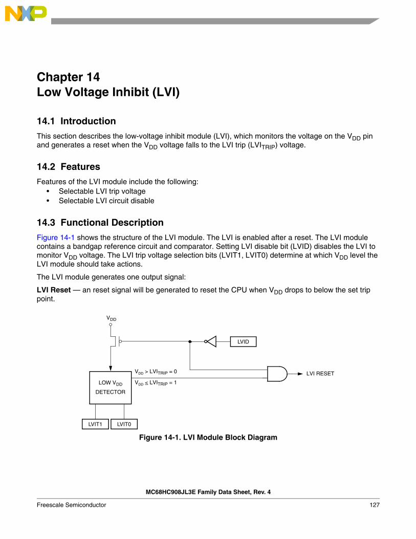
Chapter 14 Low Voltage Inhibit (LVI)
14.1 Introduction
This section describes the low-voltage inhibit module (LVI), which monitors the voltage on the VDD pin and generates a reset when the VDD voltage falls to the LVI trip (LVITRIP) voltage.
14.2 Features
Features of the LVI module include the following:• Selectable LVI trip voltage• Selectable LVI circuit disable
14.3 Functional Description
Figure 14-1 shows the structure of the LVI module. The LVI is enabled after a reset. The LVI module contains a bandgap reference circuit and comparator. Setting LVI disable bit (LVID) disables the LVI to monitor VDD voltage. The LVI trip voltage selection bits (LVIT1, LVIT0) determine at which VDD level the LVI module should take actions.
The LVI module generates one output signal:
LVI Reset — an reset signal will be generated to reset the CPU when VDD drops to below the set trip point.
Figure 14-1. LVI Module Block Diagram
LOW VDD
LVIT1
LVID
DETECTOR
VDD
LVI RESET
LVIT0
VDD > LVITRIP = 0
VDD < LVITRIP = 1
MC68HC908JL3E Family Data Sheet, Rev. 4
Freescale Semiconductor 127

Low Voltage Inhibit (LVI)
14.4 LVI Control Register (CONFIG2/CONFIG1)
The LVI module is controlled by three bits in the configuration registers, CONFIG1 and CONFIG2.
LVID — Low Voltage Inhibit Disable Bit1 = Low voltage inhibit disabled0 = Low voltage inhibit enabled
LVIT1, LVIT0 — LVI Trip Voltage SelectionThese two bits determine at which level of VDD the LVI module will come into action. LVIT1 and LVIT0 are cleared by a Power-On Reset only.
14.5 Low-Power Modes
The STOP and WAIT instructions put the MCU in low-power-consumption standby modes.
14.5.1 Wait Mode
The LVI module, when enabled, will continue to operate in WAIT Mode.
14.5.2 Stop Mode
The LVI module, when enabled, will continue to operate in STOP Mode.
Address: $001E
Bit 7 6 5 4 3 2 1 Bit 0
Read:IRQPUD R R LVIT1 LVIT0 R R R
Write:
Reset: 0 0 0 Not affected Not affected 0 0 0
POR: 0 0 0 0 0 0 0 0
R = Reserved
Figure 14-2. Configuration Register 2 (CONFIG2)
Address: $001F
Bit 7 6 5 4 3 2 1 Bit 0
Read:COPRS R R LVID R SSREC STOP COPD
Write:
Reset: 0 0 0 0 0 0 0 0
R = Reserved
Figure 14-3. Configuration Register 1 (CONFIG1)
LVIT1 LVIT0 Trip Voltage(1)
1. See Chapter 16 Electrical Specifications for full parameters.
Comments
0 0 VLVR3 (2.4V) For VDD=3V operation
0 1 VLVR3 (2.4V) For VDD=3V operation
1 0 VLVR5 (4.0V) For VDD=5V operation
1 1 Reserved
MC68HC908JL3E Family Data Sheet, Rev. 4
128 Freescale Semiconductor

Chapter 15 Break Module (BREAK)
15.1 Introduction
This section describes the break module. The break module can generate a break interrupt that stops normal program flow at a defined address to enter a background program.
15.2 Features
Features of the break module include the following:• Accessible I/O registers during the break Interrupt• CPU-generated break interrupts• Software-generated break interrupts• COP disabling during break interrupts
15.3 Functional Description
When the internal address bus matches the value written in the break address registers, the break module issues a breakpoint signal (BKPT) to the SIM. The SIM then causes the CPU to load the instruction register with a software interrupt instruction (SWI) after completion of the current CPU instruction. The program counter vectors to $FFFC and $FFFD ($FEFC and $FEFD in monitor mode).
The following events can cause a break interrupt to occur:• A CPU-generated address (the address in the program counter) matches the contents of the break
address registers.• Software writes a one to the BRKA bit in the break status and control register.
When a CPU generated address matches the contents of the break address registers, the break interrupt begins after the CPU completes its current instruction. A return from interrupt instruction (RTI) in the break routine ends the break interrupt and returns the MCU to normal operation. Figure 15-1 shows the structure of the break module.
Figure 15-1. Break Module Block Diagram
IAB[15:8]
8-BIT COMPARATOR
8-BIT COMPARATOR
CONTROL
BREAK ADDRESS REGISTER LOW
BREAK ADDRESS REGISTER HIGH
IAB[15:0]BKPT(TO SIM)
IAB[7:0]
MC68HC908JL3E Family Data Sheet, Rev. 4
Freescale Semiconductor 129

Break Module (BREAK)
15.3.1 Flag Protection During Break Interrupts
The system integration module (SIM) controls whether or not module status bits can be cleared during the break state. The BCFE bit in the break flag control register (BFCR) enables software to clear status bits during the break state. (See 5.7.3 Break Flag Control Register (BFCR) and see the Break Interrupts subsection for each module.)
15.3.2 CPU During Break Interrupts
The CPU starts a break interrupt by:• Loading the instruction register with the SWI instruction• Loading the program counter with $FFFC:$FFFD
($FEFC:$FEFD in monitor mode)
The break interrupt begins after completion of the CPU instruction in progress. If the break address register match occurs on the last cycle of a CPU instruction, the break interrupt begins immediately.
15.3.3 TIM During Break Interrupts
A break interrupt stops the timer counter.
15.3.4 COP During Break Interrupts
The COP is disabled during a break interrupt when VTST is present on the RST pin.
Addr. Register Name Bit 7 6 5 4 3 2 1 Bit 0
$FE00Break Status Register
(BSR)
Read:R R R R R R
SBSWR
Write: See note
Reset: 0
$FE03Break Flag Control
Register(BFCR)
Read:BCFE R R R R R R R
Write:
Reset: 0
$FE0CBreak Address High
Register(BRKH)
Read:Bit15 Bit14 Bit13 Bit12 Bit11 Bit10 Bit9 Bit8
Write:
Reset: 0 0 0 0 0 0 0 0
$FE0DBreak Address low
Register(BRKL)
Read:Bit7 Bit6 Bit5 Bit4 Bit3 Bit2 Bit1 Bit0
Write:
Reset: 0 0 0 0 0 0 0 0
$FE0EBreak Status and Control
Register(BRKSCR)
Read:BRKE BRKA
0 0 0 0 0 0
Write:
Reset: 0 0 0 0 0 0 0 0
Note: Writing a 0 clears SBSW. = Unimplemented R = Reserved
Figure 15-2. Break I/O Register Summary
MC68HC908JL3E Family Data Sheet, Rev. 4
130 Freescale Semiconductor

Break Module Registers
15.4 Break Module Registers
These registers control and monitor operation of the break module:• Break status and control register (BRKSCR)• Break address register high (BRKH)• Break address register low (BRKL)• Break status register (BSR)• Break flag control register (BFCR)
15.4.1 Break Status and Control Register (BRKSCR)
The break status and control register contains break module enable and status bits.
BRKE — Break Enable BitThis read/write bit enables breaks on break address register matches. Clear BRKE by writing a zero to bit 7. Reset clears the BRKE bit.
1 = Breaks enabled on 16-bit address match0 = Breaks disabled
BRKA — Break Active BitThis read/write status and control bit is set when a break address match occurs. Writing a one to BRKA generates a break interrupt. Clear BRKA by writing a zero to it before exiting the break routine. Reset clears the BRKA bit.
1 = Break address match0 = No break address match
Address: $FE0E
Bit 7 6 5 4 3 2 1 Bit 0
Read:BRKE BRKA
0 0 0 0 0 0
Write:
Reset: 0 0 0 0 0 0 0 0
= Unimplemented
Figure 15-3. Break Status and Control Register (BRKSCR)
MC68HC908JL3E Family Data Sheet, Rev. 4
Freescale Semiconductor 131

Break Module (BREAK)
15.4.2 Break Address Registers
The break address registers contain the high and low bytes of the desired breakpoint address. Reset clears the break address registers.
15.4.3 Break Status Register
The break status register contains a flag to indicate that a break caused an exit from wait mode.
SBSW — SIM Break Stop/WaitSBSW can be read within the break state SWI routine. The user can modify the return address on the stack by subtracting one from it.
1 = Wait mode was exited by break interrupt0 = Wait mode was not exited by break interrupt
Address: $FE0C
Bit 7 6 5 4 3 2 1 Bit 0
Read:Bit 15 14 13 12 11 10 9 Bit 8
Write:
Reset: 0 0 0 0 0 0 0 0
Figure 15-4. Break Address Register High (BRKH)
Address: $FE0D
Bit 7 6 5 4 3 2 1 Bit 0
Read:Bit 7 6 5 4 3 2 1 Bit 0
Write:
Reset: 0 0 0 0 0 0 0 0
Figure 15-5. Break Address Register Low (BRKL)
Address: $FE00
Bit 7 6 5 4 3 2 1 Bit 0
Read:R R R R R R
SBSWR
Write: Note(1)
Reset: 0
R = Reserved 1. Writing a zero clears SBSW.
Figure 15-6. Break Status Register (BSR)
MC68HC908JL3E Family Data Sheet, Rev. 4
132 Freescale Semiconductor

Low-Power Modes
15.4.4 Break Flag Control Register (BFCR)
The break control register contains a bit that enables software to clear status bits while the MCU is in a break state.
BCFE — Break Clear Flag Enable BitThis read/write bit enables software to clear status bits by accessing status registers while the MCU is in a break state. To clear status bits during the break state, the BCFE bit must be set.
1 = Status bits clearable during break0 = Status bits not clearable during break
15.5 Low-Power Modes
The WAIT and STOP instructions put the MCU in low-power-consumption standby modes.
15.5.1 Wait Mode
If enabled, the break module is active in wait mode. In the break routine, the user can subtract one from the return address on the stack if SBSW is set (see 5.6 Low-Power Modes). Clear the SBSW bit by writing zero to it.
15.5.2 Stop Mode
A break interrupt causes exit from stop mode and sets the SBSW bit in the break status register. See 5.7 SIM Registers.
Address: $FE03
Bit 7 6 5 4 3 2 1 Bit 0
Read:BCFE R R R R R R R
Write:
Reset: 0
R = Reserved
Figure 15-7. Break Flag Control Register (BFCR)
MC68HC908JL3E Family Data Sheet, Rev. 4
Freescale Semiconductor 133

Break Module (BREAK)
MC68HC908JL3E Family Data Sheet, Rev. 4
134 Freescale Semiconductor

Chapter 16 Electrical Specifications
16.1 Introduction
This section contains electrical and timing specifications.
16.2 Absolute Maximum Ratings
Maximum ratings are the extreme limits to which the MCU can be exposed without permanently damaging it.
NOTEThis device is not guaranteed to operate properly at the maximum ratings. Refer to 16.5 5V DC Electrical Characteristics and 16.8 3V DC Electrical Characteristics for guaranteed operating conditions.
NOTEThis device contains circuitry to protect the inputs against damage due to high static voltages or electric fields; however, it is advised that normal precautions be taken to avoid application of any voltage higher than maximum-rated voltages to this high-impedance circuit. For proper operation, it is recommended that VIN and VOUT be constrained to the range VSS ≤ (VIN or VOUT) ≤ VDD. Reliability of operation is enhanced if unused inputs are connected to an appropriate logic voltage level (for example, either VSS or VDD.)
Table 16-1. Absolute Maximum Ratings
Characteristic(1)
1. Voltages referenced to VSS.
Symbol Value Unit
Supply voltage VDD –0.3 to +6.0 V
Input voltage VIN VSS–0.3 to VDD +0.3 V
Mode entry voltage, IRQ pin VTST VSS–0.3 to +8.5 V
Maximum current per pin excluding VDD and VSS I ±25 mA
Storage temperature TSTG –55 to +150 °C
Maximum current out of VSS IMVSS 100 mA
Maximum current into VDD IMVDD 100 mA
MC68HC908JL3E Family Data Sheet, Rev. 4
Freescale Semiconductor 135

Electrical Specifications
16.3 Functional Operating Range
16.4 Thermal Characteristics
Table 16-2. Operating Range
Characteristic Symbol Value Unit
Operating temperature range TA – 40 to +125 – 40 to +85 °C
Operating voltage range VDD 5 ±10% 3 ±10% V
Table 16-3. Thermal Characteristics
Characteristic Symbol Value Unit
Thermal resistance20-pin PDIP20-pin SOIC28-pin PDIP28-pin SOIC48-pin LQFP
θJA
7070707080
°C/W°C/W°C/W°C/W°C/W
I/O pin power dissipation PI/O User determined W
Power dissipation(1)
1. Power dissipation is a function of temperature.
PDPD = (IDD × VDD) + PI/O =
K/(TJ + 273 °C)W
Constant(2)
2. K constant unique to the device. K can be determined for a known TA and measured PD. With this value of K, PD and TJcan be determined for any value of TA.
KPD x (TA + 273 °C)
+ PD2
× θJAW/°C
Average junction temperature TJ TA + (PD × θJA) °C
MC68HC908JL3E Family Data Sheet, Rev. 4
136 Freescale Semiconductor

5V DC Electrical Characteristics
16.5 5V DC Electrical Characteristics
Table 16-4. DC Electrical Characteristics (5V)
Characteristic(1) Symbol Min Typ(2) Max Unit
Output high voltage (ILOAD = –2.0mA)PTA0–PTA6, PTB0–PTB7, PTD0–PTD7
VOH VDD–0.8 — — V
Output low voltage (ILOAD = 1.6mA)PTA6, PTB0–PTB7, PTD0, PTD1, PTD4, PTD5
VOL — — 0.4 V
Output low voltage (ILOAD = 25mA)PTD6, PTD7
VOL — — 0.5 V
LED drives (VOL = 3V)PTA0–PTA5, PTD2, PTD3, PTD6, PTD7
IOL 10 16 22 mA
Input high voltagePTA0–PTA6, PTB0–PTB7, PTD0–PTD7,
RST, IRQ, OSC1VIH 0.7 × VDD — VDD V
Input low voltagePTA0–PTA6, PTB0–PTB7, PTD0–PTD7,
RST, IRQ, OSC1VIL VSS — 0.3 × VDD V
VDD supply current, fOP = 4MHzRun(3)
MC68HC908JL3E/JK3E/JK1EMC68HRC908JL3E/JK3E/JK1E
Wait(4)
MC68HC908JL3E/JK3E/JK1EMC68HRC908JL3E/JK3E/JK1E
Stop(5)
(–40°C to 85°C)MC68HC908JL3E/JK3E/JK1EMC68HRC908JL3E/JK3E/JK1E
(–40°C to 125°C)MC68HC908JL3E/JK3E/JK1EMC68HRC908JL3E/JK3E/JK1E
IDD
——
——
——
——
104.5
61
22
22
115
6.51.5
55
1010
mAmA
mAmA
μAμA
μAμA
Digital I/O ports Hi-Z leakage current IIL — — ± 10 μA
Input current IIN — — ± 1 μA
CapacitancePorts (as input or output)
COUT
CIN
——
——
128
pF
POR rearm voltage(6) VPOR 0 — 100 mV
POR rise time ramp rate(7) RPOR 0.035 — — V/ms
Monitor mode entry voltage VTST 1.5 × VDD — 8.5 V
Pullup resistors(8)
PTD6, PTD7RST, IRQ, PTA0–PTA6
RPU1RPU2
1.816
3.326
4.836
kΩkΩ
Table continued on next page
MC68HC908JL3E Family Data Sheet, Rev. 4
Freescale Semiconductor 137

Electrical Specifications
16.6 5V Control Timing
LVI reset voltage VLVR5 3.6 4.0 4.4 V
1. VDD = 4.5 to 5.5 Vdc, VSS = 0 Vdc, TA = TL to TH, unless otherwise noted.2. Typical values reflect average measurements at midpoint of voltage range, 25 °C only.3. Run (operating) IDD measured using external square wave clock source (fOP = 4MHz). All inputs 0.2V from rail. No dc
loads. Less than 100 pF on all outputs. CL = 20 pF on OSC2. All ports configured as inputs. OSC2 capacitance linearlyaffects run IDD. Measured with all modules enabled.
4. Wait IDD measured using external square wave clock source (fOP = 4MHz). All inputs 0.2V from rail. No dc loads. Lessthan 100 pF on all outputs. CL = 20 pF on OSC2. All ports configured as inputs. OSC2 capacitance linearly affectswait IDD.
5. Stop IDD measured with OSC1 grounded; no port pins sourcing current. LVI is disabled.6. Maximum is highest voltage that POR is guaranteed.7. If minimum VDD is not reached before the internal POR reset is released, RST must be driven low externally until
minimum VDD is reached.8. RPU1 and RPU2 are measured at VDD = 5.0V.
Table 16-5. Control Timing (5V)
Characteristic(1)
1. VDD = 4.5 to 5.5 Vdc, VSS = 0 Vdc, TA = TL to TH; timing shown with respect to 20% VDD and 70% VSS, unless otherwisenoted.
Symbol Min Max Unit
Internal operating frequency(2)
2. Some modules may require a minimum frequency greater than dc for proper operation; see appropriate table for thisinformation.
fOP — 8 MHz
RST input pulse width low(3)
3. Minimum pulse width reset is guaranteed to be recognized. It is possible for a smaller pulse width to cause a reset.
tIRL 750 — ns
Table 16-4. DC Electrical Characteristics (5V) (Continued)
Characteristic(1) Symbol Min Typ(2) Max Unit
MC68HC908JL3E Family Data Sheet, Rev. 4
138 Freescale Semiconductor

5V Oscillator Characteristics
16.7 5V Oscillator Characteristics
Figure 16-1. RC vs. Frequency (5V @25°C)
Table 16-6. Oscillator Component Specifications (5V)
Characteristic Symbol Min Typ Max Unit
Crystal frequency, XTALCLK fOSCXCLK — 10 32 MHz
RC oscillator frequency, RCCLK fRCCLK 2 10 12 MHz
External clock
reference frequency(1)
1. No more than 10% duty cycle deviation from 50%.
fOSCXCLK dc — 32 MHz
Crystal load capacitance(2)
2. Consult crystal vendor data sheet.
CL — — —
Crystal fixed capacitance(2) C1 — 2 × CL —
Crystal tuning capacitance(2) C2 — 2 × CL —
Feedback bias resistor RB — 10 MΩ —
Series resistor(2), (3)
3. Not required for high frequency crystals.
RS — — —
RC oscillator external R REXT See Figure 16-1
RC oscillator external C CEXT — 10 — pF
REXT CEXT
OSC1
VDD
MCU
0
0 10 20 30 40 50
14
12
10
8
6
4
2
RESISTOR, REXT (kΩ)
RC
FR
EQU
ENC
Y, f R
CC
LK (M
Hz) CEXT = 10 pF
5V @ 25°C
MC68HC908JL3E Family Data Sheet, Rev. 4
Freescale Semiconductor 139

Electrical Specifications
16.8 3V DC Electrical Characteristics
Table 16-7. DC Electrical Characteristics (3V)
Characteristic(1) Symbol Min Typ(2) Max Unit
Output high voltage (ILOAD = –1.0mA)PTA0–PTA6, PTB0–PTB7, PTD0–PTD7
VOH VDD– 0.4 — — V
Output low voltage (ILOAD = 0.8mA)PTA6, PTB0–PTB7, PTD0, PTD1, PTD4, PTD5
VOL — — 0.4 V
Output low voltage (ILOAD = 20mA)PTD6, PTD7
VOL — — 0.5 V
LED drives (VOL = 1.8V)PTA0–PTA5, PTD2, PTD3, PTD6, PTD7
IOL 3 6 10 mA
Input high voltagePTA0–PTA6, PTB0–PTB7, PTD0–PTD7,
RST, IRQ, OSC1VIH 0.7 × VDD — VDD V
Input low voltagePTA0–PTA6, PTB0–PTB7, PTD0–PTD7,
RST, IRQ, OSC1VIL VSS — 0.3 × VDD V
VDD supply current, fOP = 2MHzRun(3)
MC68HC908JL3E/JK3E/JK1EMC68HRC908JL3E/JK3E/JK1E
Wait(4)
MC68HC908JL3E/JK3E/JK1EMC68HRC908JL3E/JK3E/JK1E
Stop(5)
(–40°C to 85°C)MC68HC908JL3E/JK3E/JK1EMC68HRC908JL3E/JK3E/JK1E
IDD
——
——
——
31.5
1.50.2
11
3.52
20.3
55
mAmA
mAmA
μAμA
Digital I/O ports Hi-Z leakage current IIL — — ± 10 μA
Input current IIN — — ± 1 μA
CapacitancePorts (as input or output)
COUT
CIN
——
——
128
pF
POR rearm voltage(6) VPOR 0 — 100 mV
POR rise time ramp rate(7) RPOR 0.035 — — V/ms
Monitor mode entry voltage VTST 1.5 × VDD — 8.5 V
Pullup resistors(8)
PTD6, PTD7RST, IRQ, PTA0–PTA6
RPU1RPU2
1.816
3.326
4.836
kΩkΩ
Table continued on next page
MC68HC908JL3E Family Data Sheet, Rev. 4
140 Freescale Semiconductor

3V Control Timing
16.9 3V Control Timing
LVI reset voltage VLVR3 2.0 2.4 2.69 V
1. VDD = 2.7 to 3.3 Vdc, VSS = 0 Vdc, TA = TL to TH, unless otherwise noted.2. Typical values reflect average measurements at midpoint of voltage range, 25 °C only.3. Run (operating) IDD measured using external square wave clock source (fOP = 2MHz). All inputs 0.2V from rail. No dc
loads. Less than 100 pF on all outputs. CL = 20 pF on OSC2. All ports configured as inputs. OSC2 capacitance linearlyaffects run IDD. Measured with all modules enabled.
4. Wait IDD measured using external square wave clock source (fOP = 2MHz). All inputs 0.2V from rail. No dc loads. Lessthan 100 pF on all outputs. CL = 20 pF on OSC2. All ports configured as inputs. OSC2 capacitance linearly affects wait IDD.
5. Stop IDD measured with OSC1 grounded; no port pins sourcing current. LVI is disabled.6. Maximum is highest voltage that POR is guaranteed.7. If minimum VDD is not reached before the internal POR reset is released, RST must be driven low externally until minimum
VDD is reached.8. RPU1 and RPU2 are measured at VDD = 5.0V.
Table 16-8. Control Timing (3V)
Characteristic(1)
1. VDD = 2.7 to 3.3 Vdc, VSS = 0 Vdc, TA = TL to TH; timing shown with respect to 20% VDD and 70% VDD, unless otherwisenoted.
Symbol Min Max Unit
Internal operating frequency(2)
2. Some modules may require a minimum frequency greater than dc for proper operation; see appropriate table for this infor-mation.
fOP — 4 MHz
RST input pulse width low(3)
3. Minimum pulse width reset is guaranteed to be recognized. It is possible for a smaller pulse width to cause a reset.
tIRL 1.5 — μs
Table 16-7. DC Electrical Characteristics (3V) (Continued)
Characteristic(1) Symbol Min Typ(2) Max Unit
MC68HC908JL3E Family Data Sheet, Rev. 4
Freescale Semiconductor 141

Electrical Specifications
16.10 3V Oscillator Characteristics
Figure 16-2. RC vs. Frequency (3V @25°C)
Table 16-9. Oscillator Component Specifications (3V)
Characteristic Symbol Min Typ Max Unit
Crystal frequency, XTALCLK fOSCXCLK — 8 16 MHz
RC oscillator frequency, RCCLK fRCCLK 2 8 12 MHz
External clock reference frequency(1)
1. No more than 10% duty cycle deviation from 50%.
fOSCXCLK dc — 16 MHz
Crystal load capacitance(2)
2. Consult crystal vendor data sheet.
CL — — —
Crystal fixed capacitance(2) C1 — 2 × CL —
Crystal tuning capacitance(2) C2 — 2 × CL —
Feedback bias resistor RB — 10 MΩ —
Series resistor(2), (3)
3. Not required for high frequency crystals.
RS — — —
RC oscillator external R REXT See Figure 16-2
RC oscillator external C CEXT — 10 — pF
REXT CEXT
OSC1
VDD
MCU
0
0 10 20 30 40 50
14
12
10
8
6
4
2
RESISTOR, REXT (kΩ)
RC
FR
EQU
ENC
Y, f R
CC
LK (M
Hz) CEXT = 10 pF
3V @ 25°C
MC68HC908JL3E Family Data Sheet, Rev. 4
142 Freescale Semiconductor

Typical Supply Currents
16.11 Typical Supply Currents
Figure 16-3. Typical Operating IDD (MC68HC908JL3E/JK3E/JK1E), with All Modules Turned On (25°C)
Figure 16-4. Typical Operating IDD (MC68HRC908JL3E/JK3E/JK1E), with All Modules Turned On (25°C)
Figure 16-5. Typical Wait Mode IDD (MC68HC908JL3E/JK3E/JK1E), with All Modules Turned Off (25°C)
0
2
4
6
8
10
12
0 1 2 3 4 5 6 7 8 9fOP or fBUS (MHz)
I DD
(mA)
14
MC68HC908JL3E/JK3E/JK1E
5.5 V3.3 V
0
2
4
6
8
10
0 1 2 3 4 5 6 7 8 9fOP or fBUS (MHz)
I DD
(mA)
MC68HRC908JL3E/JK3E/JK1E
5.5 V3.3 V
0
2
4
6
8
10
0 1 2 3 4 5 6 7 8 9fOP or fBUS (MHz)
I DD
(mA)
MC68HC908JL3E/JK3E/JK1E
5.5 V3.3 V
MC68HC908JL3E Family Data Sheet, Rev. 4
Freescale Semiconductor 143

Electrical Specifications
Figure 16-6. Typical Wait Mode IDD (MC68HRC908JL3E/JK3E/JK1E), with All Modules Turned Off (25 °C)
16.12 ADC Characteristics
Table 16-10. ADC Characteristics
Characteristic Symbol Min Max Unit Comments
Supply voltage VDDAD2.7
(VDD min)5.5
(VDD max) V
Input voltages VADIN VSS VDD V
Resolution BAD 8 8 Bits
Absolute accuracy AAD ± 0.5 ± 1.5 LSB Includes quantization
ADC internal clock fADIC 0.5 1.048 MHztAIC = 1/fADIC, tested
only at 1 MHz
Conversion range RAD VSS VDD V
Power-up time tADPU 16 tAIC cycles
Conversion time tADC 14 15 tAIC cycles
Sample time(1)
1. Source impedances greater than 10 kΩ adversely affect internal RC charging time during input sampling.
tADS 5 — tAIC cycles
Zero input reading(2)
2. Zero-input/full-scale reading requires sufficient decoupling measures for accurate conversions.
ZADI 00 01 Hex VIN = VSS
Full-scale reading(3) FADI FE FF Hex VIN = VDD
Input capacitance CADI — (20) 8 pF Not tested
Input leakage(3)
Port B/port D
3. The external system error caused by input leakage current is approximately equal to the product of R source and inputcurrent.
— — ± 1 μA
0
0.25
0.5
0.75
1
1.25
1.50
1.75
2
0 1 2 3 4 5 6 7 8
I DD
(mA)
fOP or fBUS (MHz)
MC68HRC908JL3E/JK3E/JK1E
5.5 V3.3 V
MC68HC908JL3E Family Data Sheet, Rev. 4
144 Freescale Semiconductor

Memory Characteristics
16.13 Memory Characteristics
Table 16-11. Memory Characteristics
Characteristic Symbol Min Max Unit
RAM data retention voltage VRDR 1.3 — V
Flash program bus clock frequency — 1 — MHz
Flash read bus clock frequency fRead(1)
1. fRead is defined as the frequency range for which the Flash memory can be read.
32k 8M Hz
Flash page erase time tErase(2)
2. If the page erase time is longer than tErase (Min), there is no erase-disturb, but it reduces the endurance of the Flash mem-ory.
1 — ms
Flash mass erase time tMErase(3)
3. If the mass erase time is longer than tMErase (Min), there is no erase-disturb, but it reduces the endurance of the Flashmemory.
4 — ms
Flash PGM/ERASE to HVEN set up time tnvs 10 — μs
Flash high-voltage hold time tnvh 5 — μs
Flash high-voltage hold time (mass erase) tnvh1 100 — μs
Flash program hold time tpgs 5 — μs
Flash program time tPROG 30 40 μs
Flash return to read time trcv(4)
4. trcv is defined as the time it needs before the Flash can be read after turning off the high voltage charge pump, by clearingHVEN to 0.
1 — μs
Flash cumulative program hv period tHV(5)
5. tHV is defined as the cumulative high voltage programming time to the same row before next erase.tHV must satisfy this condition: tnvs + tnvh + tpgs + (tPROG × 32) ≤ tHV max.
— 4 ms
Flash row erase endurance(6)
6. The minimum row endurance value specifies each row of the Flash memory is guaranteed to work for at least this manyerase / program cycles.
— 10k — cycles
Flash row program endurance(7)
7. The minimum row endurance value specifies each row of the Flash memory is guaranteed to work for at least this manyerase / program cycles.
— 10k — cycles
Flash data retention time(8)
8. The Flash is guaranteed to retain data over the entire operating temperature range for at least the minimum time specified.
— 10 — years
MC68HC908JL3E Family Data Sheet, Rev. 4
Freescale Semiconductor 145

Electrical Specifications
MC68HC908JL3E Family Data Sheet, Rev. 4
146 Freescale Semiconductor

Chapter 17 Mechanical Specifications
17.1 Introduction
This section gives the dimensions for:• 20-pin plastic dual in-line package (case #738)• 20-pin small outline integrated circuit package (case #751D)• 28-pin plastic dual in-line package (case #710)• 28-pin small outline integrated circuit package (case #751F)• 48-pin low-profile quad flat pack (case #932)
The following figures show the latest package drawings at the time of this publication. To make sure that you have the latest package specifications, contact your local Freescale Sales Office.
17.2 Package Dimensions
Refer to the following pages for detailed package dimensions.
20-Pin PDIP (Case #738)
NOTES:1. DIMENSIONING AND TOLERANCING PER ANSI
Y14.5M, 1982.2. CONTROLLING DIMENSION: INCH.3. DIMENSION L TO CENTER OF LEAD WHEN
FORMED PARALLEL.4. DIMENSION B DOES NOT INCLUDE MOLD
FLASH.
M
L
J 20 PL
MBM0.25 (0.010) T
DIM MIN MAX MIN MAXMILLIMETERSINCHES
A 25.66 27.171.010 1.070B 6.10 6.600.240 0.260C 3.81 4.570.150 0.180D 0.39 0.550.015 0.022
G 2.54 BSC0.100 BSCJ 0.21 0.380.008 0.015K 2.80 3.550.110 0.140L 7.62 BSC0.300 BSCM 0 15 0 15 N 0.51 1.010.020 0.040
� �� �
E1.27 1.770.050 0.070
1
11
10
20
–A–
SEATINGPLANE
K
N
FG
D 20 PL
–T–
MAM0.25 (0.010) T
E
B
C
F1.27 BSC0.050 BSC
MC68HC908JL3E Family Data Sheet, Rev. 4
Freescale Semiconductor 147


Mechanical Specifications
MC68HC908JL3E Family Data Sheet, Rev. 4
156 Freescale Semiconductor
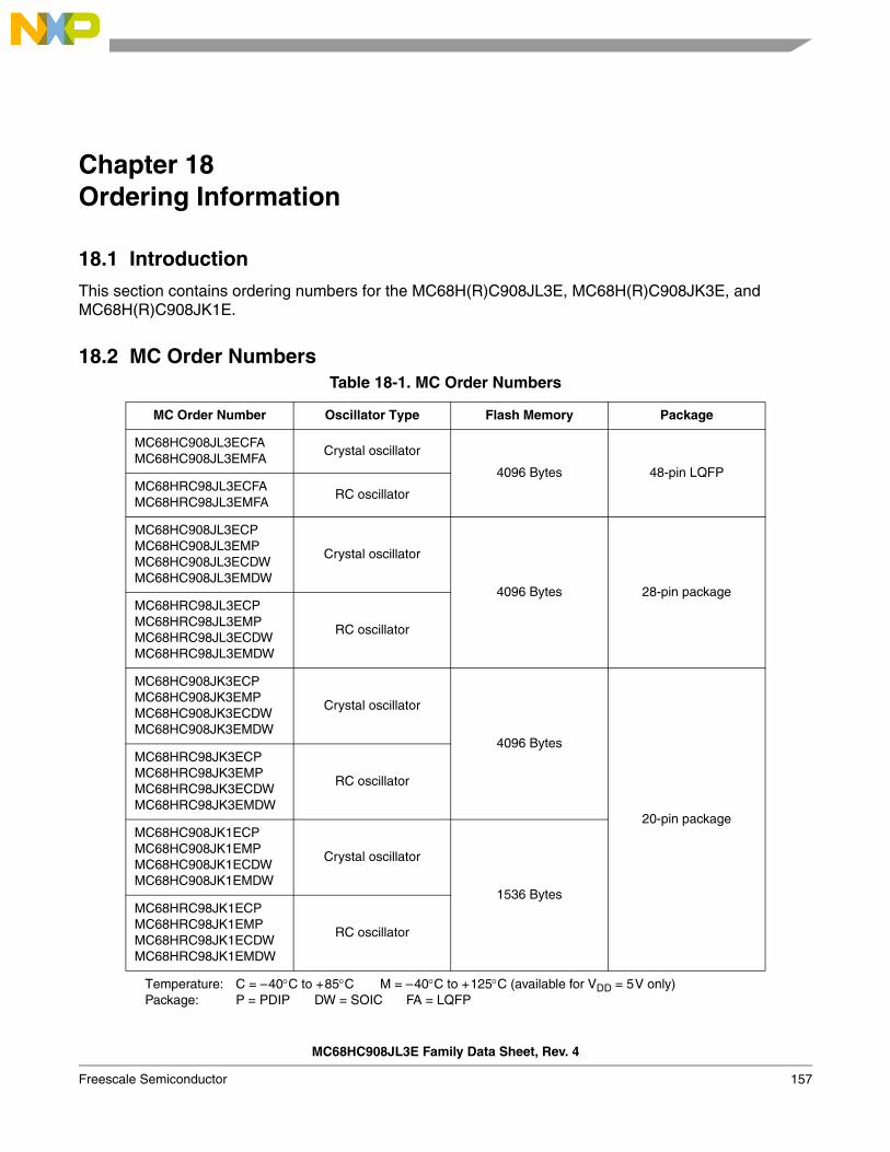
Chapter 18 Ordering Information
18.1 Introduction
This section contains ordering numbers for the MC68H(R)C908JL3E, MC68H(R)C908JK3E, and MC68H(R)C908JK1E.
18.2 MC Order NumbersTable 18-1. MC Order Numbers
MC Order Number Oscillator Type Flash Memory Package
MC68HC908JL3ECFAMC68HC908JL3EMFA
Crystal oscillator
4096 Bytes 48-pin LQFPMC68HRC98JL3ECFAMC68HRC98JL3EMFA
RC oscillator
MC68HC908JL3ECPMC68HC908JL3EMPMC68HC908JL3ECDWMC68HC908JL3EMDW
Crystal oscillator
4096 Bytes 28-pin packageMC68HRC98JL3ECPMC68HRC98JL3EMPMC68HRC98JL3ECDWMC68HRC98JL3EMDW
RC oscillator
MC68HC908JK3ECPMC68HC908JK3EMPMC68HC908JK3ECDWMC68HC908JK3EMDW
Crystal oscillator
4096 Bytes
20-pin package
MC68HRC98JK3ECPMC68HRC98JK3EMPMC68HRC98JK3ECDWMC68HRC98JK3EMDW
RC oscillator
MC68HC908JK1ECPMC68HC908JK1EMPMC68HC908JK1ECDWMC68HC908JK1EMDW
Crystal oscillator
1536 BytesMC68HRC98JK1ECPMC68HRC98JK1EMPMC68HRC98JK1ECDWMC68HRC98JK1EMDW
RC oscillator
Temperature: C = –40°C to +85°C M = –40°C to +125°C (available for VDD = 5V only)Package: P = PDIP DW = SOIC FA = LQFP
MC68HC908JL3E Family Data Sheet, Rev. 4
Freescale Semiconductor 157

Ordering Information
MC68HC908JL3E Family Data Sheet, Rev. 4
158 Freescale Semiconductor

Appendix A MC68HLC908JL3E/JK3E/JK1E
A.1 Introduction
This appendix introduces three devices, that are low-voltage versions of MC68HC908JL3E/JK3E/JK1E:• MC68HLC908JL3E• MC68HLC908JK3E• MC68HLC908JK1E
The entire data book apply to these low-voltage devices, with exceptions outlined in this appendix.
A.2 Flash Memory
The Flash memory can be read at minimum VDD of 2.2V. Program or erase operations require a minimum VDD of 2.7V.
A.3 Low-Voltage Inhibit
There is no low-voltage inhibit circuit. Therefore, no low-voltage reset. The associated register bits are reserved bits.
A.4 Oscillator Options
Only crystal oscillator or direct clock input is supported.
A.5 Electrical Specifications
Electrical specifications for low-voltage devices are given in the following tables.
A.5.1 Functional Operating Range
Table A-1. Operating Range
Characteristic Symbol Value Unit
Operating temperature range TA 0 to +85 °C
Operating voltage range VDD 2.2 to 5.5 V
Operating voltage for Flash memory program and erase operations VDD 2.7 to 5.5 V
MC68HC908JL3E Family Data Sheet, Rev. 4
Freescale Semiconductor 159

A.5.2 DC Electrical Characteristics
Table A-2. DC Electrical Characteristics
Characteristic(1)
1. VDD = 2.4 Vdc, VSS = 0 Vdc, TA = TL to TH, unless otherwise noted.
Symbol Min Typ(2)
2. Typical values reflect average measurements at midpoint of voltage range, 25 °C only.
Max Unit
Output high voltage (ILOAD = –1.0mA)PTA0–PTA6, PTB0–PTB7, PTD0–PTD7
VOH VDD– 0.4 — — V
Output low voltage (ILOAD = 0.8mA)PTA6, PTB0–PTB7, PTD0, PTD1, PTD4, PTD5
VOL — — 0.4 V
Output low voltage (ILOAD = 15mA)PTD6, PTD7
VOL — — 0.5 V
Input high voltagePTA0–PTA6, PTB0–PTB7, PTD0–PTD7,
RST, IRQ, OSC1VIH 0.7 × VDD — VDD V
Input low voltagePTA0–PTA6, PTB0–PTB7, PTD0–PTD7,
RST, IRQ, OSC1VIL VSS — 0.2 × VDD V
VDD supply current (VDD = 2.4V, fOP = 2MHz)Run(3)
Wait(4)
Stop(5) 0°C to 85°C
3. Run (operating) IDD measured using external square wave clock source. All inputs 0.2 V from rail. No dc loads. Less than100 pF on all outputs. CL = 20 pF on OSC2. All ports configured as inputs. OSC2 capacitance linearly affects run IDD.Measured with all modules enabled.
4. Wait IDD measured using external square wave clock source; all inputs 0.2 V from rail; no dc loads; less than 100 pF onall outputs. CL = 20 pF on OSC2; all ports configured as inputs; OSC2 capacitance linearly affects wait IDD.
5. STOP IDD measured with OSC1 grounded, no port pins sourcing current. LVI is disabled.
IDD———
211
3.51.53
mAmAμA
Digital I/O ports Hi-Z leakage current IIL — — ± 10 μA
Input current IIN — — ± 1 μA
CapacitancePorts (as input or output)
COUT
CIN
——
——
128
pF
POR rearm voltage(6)
6. Maximum is highest voltage that POR is guaranteed.
VPOR 0 — 100 mV
POR rise time ramp rate(7)
7. If minimum VDD is not reached before the internal POR reset is released, RST must be driven low externally until minimumVDD is reached.
RPOR 0.02 — — V/ms
Pullup resistors(8)
PTD6, PTD7RST, IRQ, PTA0–PTA6
8. RPU1 and RPU2 are measured at VDD = 5.0V
RPU1
RPU2
1.816
3.326
4.836
kΩkΩ
MC68HC908JL3E Family Data Sheet, Rev. 4
160 Freescale Semiconductor

A.5.3 Control Timing
A.5.4 Oscillator Characteristics
Table A-3. Control Timing
Characteristic(1)
1. VDD = 2.2 Vdc, VSS = 0 Vdc, TA = TL to TH; timing shown with respect to 20% VDD and 70% VDD, unless otherwise noted.
Symbol Min Max Unit
Internal operating frequency(2)
2. Some modules may require a minimum frequency greater than dc for proper operation; see appropriate table for this infor-mation.
fOP — 2 MHz
RST input pulse width low(3)
3. Minimum pulse width reset is guaranteed to be recognized. It is possible for a smaller pulse width to cause a reset.
tIRL 1.5 — μs
Table A-4. Oscillator Component Specifications
Characteristic Symbol Min Typ Max Unit
Crystal frequency, XTALCLK fOSCXCLK — — 8 MHz
External clock reference frequency(1)
1. No more than 10% duty cycle deviation from 50%
fOSCXCLK dc — 8 MHz
Crystal load capacitance(2)
2. Consult crystal vendor data sheet
CL — — —
Crystal fixed capacitance(2) C1 — 2 × CL —
Crystal tuning capacitance(2) C2 — 2 × CL —
Feedback bias resistor RB — 10 MΩ —
Series resistor(2), (3)
3. Not Required for high frequency crystals
RS — — —
MC68HC908JL3E Family Data Sheet, Rev. 4
Freescale Semiconductor 161

A.5.5 ADC Characteristics
Table A-5. ADC Characteristics
Characteristic Symbol Min Max Unit Comments
Supply voltage VDDAD2.2
(VDD min)5.5
(VDD max) V
Input voltages VADIN VSS VDD V
Resolution BAD 8 8 Bits
Absolute accuracy AAD ± 0.5 ± 2 LSB Includes quantization
ADC internal clock fADIC 0.5 1.048 MHztAIC = 1/fADIC, tested
only at 1 MHz
Conversion range RAD VSS VDD V
Power-up time tADPU 14 — tAIC cycles
Conversion time tADC 14 15 tAIC cycles
Sample time(1)
1. Source impedances greater than 10 kΩ adversely affect internal RC charging time during input sampling.
tADS 5 — tAIC cycles
Zero input reading(2)
2. Zero-input/full-scale reading requires sufficient decoupling measures for accurate conversions.
ZADI 00 01 Hex VIN = VSS
Full-scale reading(3) FADI FE FF Hex VIN = VDD
Input capacitance CADI — (20) 8 pF Not tested
Input leakage(3)
Port B/port D
3. The external system error caused by input leakage current is approximately equal to the product of R source and inputcurrent.
— — ± 1 μA
MC68HC908JL3E Family Data Sheet, Rev. 4
162 Freescale Semiconductor

A.5.6 Memory Characteristics
The Flash memory can only be read at an operating voltage of 2.2 to 5.5V. Program and erase are achieved at an operating voltage of 2.7 to 5.5V. The program and erase parameters in Table A-6 are forVDD = 2.7 to 5.5V only.
Table A-6. Memory Characteristics
Characteristic Symbol Min Max Unit
RAM data retention voltage VRDR 1.3 — V
Flash program bus clock frequency — 1 — MHz
Flash read bus clock frequency fRead(1)
1. fRead is defined as the frequency range for which the Flash memory can be read.
32k 8M Hz
Flash page erase time tErase(2)
2. If the page erase time is longer than tErase (Min), there is no erase-disturb, but it reduces the endurance of the Flash mem-ory.
1 — ms
Flash mass erase time tMErase(3)
3. If the mass erase time is longer than tMErase (Min), there is no erase-disturb, but it reduces the endurance of the Flashmemory.
4 — ms
Flash PGM/ERASE to HVEN set up time tnvs 10 — μs
Flash high-voltage hold time tnvh 5 — μs
Flash high-voltage hold time (mass erase) tnvhl 100 — μs
Flash program hold time tpgs 5 — μs
Flash program time tPROG 30 40 μs
Flash return to read time trcv(4)
4. trcv is defined as the time it needs before the Flash can be read after turning off the high voltage charge pump, by clearingHVEN to 0.
1 — μs
Flash cumulative program hv period tHV(5)
5. tHV is defined as the cumulative high voltage programming time to the same row before next erase.tHV must satisfy this condition: tnvs + tnvh + tpgs + (tPROG × 32) ≤ tHV max.
— 4 ms
Flash row erase endurance(6)
6. The minimum row endurance value specifies each row of the Flash memory is guaranteed to work for at least this manyerase / program cycles.
— 10k — cycles
Flash row program endurance(7)
7. The minimum row endurance value specifies each row of the Flash memory is guaranteed to work for at least this manyerase / program cycles.
— 10k — cycles
Flash data retention time(8)
8. The Flash is guaranteed to retain data over the entire operating temperature range for at least the minimum time specified.
— 10 — years
MC68HC908JL3E Family Data Sheet, Rev. 4
Freescale Semiconductor 163

A.6 MC Order Numbers
Table A-7 shows the ordering numbers for the low-voltage devices.
Table A-7. MC68HLC908JL3E/JK3E/JK1E Order Numbers
MC Order Number Oscillator Type Flash Memory Package
MC68HLC98JL3EIFA Crystal oscillator 4096 Bytes 48-pin LQFP
MC68HLC98JL3EIPMC68HLC98JL3EIDW
Crystal oscillator 4096 Bytes 28-pin package
MC68HLC98JK3EIPMC68HLC98JK3EIDW
Crystal oscillator 4096 Bytes
20-pin packageMC68HLC98JK1EIPMC68HLC98JK1EIDW
Crystal oscillator 1536 Bytes
Notes:I = 0 °C to +85 °CP = Plastic dual in-line package (PDIP)DW = Small outline integrated circuit package (SOIC)FA = Low-Profile Quad Flat Pack (LQFP)
MC68HC908JL3E Family Data Sheet, Rev. 4
164 Freescale Semiconductor

Appendix B MC68H(R)C08JL3E/JK3E
B.1 Introduction
This appendix introduces four devices, that are ROM versions of MC68H(R)C908JL3E/JK3E:• MC68HC08JL3E• MC68HC08JK3E• MC68HRC08JL3E• MC68HRC08JK3E
The entire data book apply to these ROM devices, with exceptions outlined in this appendix.
B.2 MCU Block Diagram
Figure B-1 shows the block diagram of the MC68H(R)C08JL3E/JK3E.
Table B-1. Summary of Device Differences
MC68H(R)C08JL3E/JK3E MC68H(R)C908JL3E/JK3E
Memory ($EC00–$FBFF) 4,096 bytes ROM 4,096 bytes Flash
User vectors ($FFD0–$FFFF) 48 bytes ROM 48 bytes Flash
Registers at $FE08 and $FE09Not used; locations are reserved.
Flash related registers.$FE08 — FLCR$FF09 — FLBPR
Monitor ROM($FC00–$FDFF and $FE10–$FFCF)
$FC00–$FDFF: Not used.$FE10–$FFCF: Used for testing purposes only.
Used for testing and Flash programming/erasing.
MC68HC908JL3E Family Data Sheet, Rev. 4
Freescale Semiconductor 165
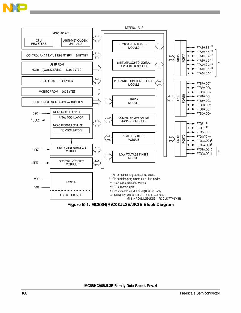
Figure B-1. MC68H(R)C08JL3E/JK3E Block Diagram
SYSTEM INTEGRATIONMODULE
ARITHMETIC/LOGICUNIT (ALU)
CPUREGISTERS
M68HC08 CPU
CONTROL AND STATUS REGISTERS — 64 BYTES
USER ROM:
USER RAM — 128 BYTES
MONITOR ROM — 960 BYTES
USER ROM VECTOR SPACE — 48 BYTES
EXTERNAL INTERRUPTMODULE
INTERNAL BUS
* RST
* IRQ
POWER
VSS
2-CHANNEL TIMER INTERFACEMODULE
KEYBOARD INTERRUPTMODULE
8-BIT ANALOG-TO-DIGITALCONVERTER MODULE
VDD
ADC REFERENCE
DD
RB
POR
TB
PTB7/ADC7PTB6/ADC6PTB5/ADC5PTB4/ADC4PTB3/ADC3PTB2/ADC2PTB1/ADC1PTB0/ADC0
DD
RA
POR
TA
PTA6/KBI6**¥
PTA5/KBI5**‡
PTA4/KBI4**‡
PTA3/KBI3**‡
PTA2/KBI2**‡
PTA1/KBI1**‡
PTA0/KBI0**‡
LOW-VOLTAGE INHIBITMODULE
* Pin contains integrated pull-up device.** Pin contains programmable pull-up device.† 25mA open-drain if output pin.‡ LED direct sink pin.
OSC1
¥ OSC2X-TAL OSCILLATOR
RC OSCILLATOR
DD
RD
POR
TD
PTD7**†‡
PTD6**†‡
PTD5/TCH1PTD4/TCH0PTD3/ADC8‡
PTD2/ADC9‡
PTD1/ADC10PTD0/ADC11
COMPUTER OPERATINGPROPERLY MODULE
POWER-ON RESETMODULE
BREAKMODULE
#
#
# Pins available on MC68H(R)C08JL3E only.
MC68HRC908JL3E/JK3E
MC68HC908JL3E/JK3E
¥ Shared pin:MC68HRC08JL3E/JK3E — RCCLK/PTA6/KBI6
MC68H(R)C08JK3E/JL3E — 4,096 BYTES
MC68HC08JL3E/JK3E — OSC2
MC68HC908JL3E Family Data Sheet, Rev. 4
166 Freescale Semiconductor

B.3 Memory Map
The MC68H(R)C08JL3E/JK3E has 4,096 bytes of user ROM from $EC00 to $FBFF, and 48 bytes of user ROM vectors from $FFD0 to $FFFF. On the MC68H(R)C908JL3E/JK3E, these memory locations are Flash memory.
Figure B-2 shows the memory map of the MC68H(R)C08JL3E/JK3E.
$0000↓
$003F
I/O REGISTERS64 BYTES
$0040↓
$007F
RESERVED64 BYTES
$0080↓
$00FF
RAM128 BYTES
$0100↓
$EBFF
UNIMPLEMENTED60,160 BYTES
$EC00↓
$FBFF
ROMMC68H(R)C08JL3E/JK3E
4,096 BYTES
$FC00↓
$FDFF
MONITOR ROM512 BYTES
$FE00 BREAK STATUS REGISTER (BSR)
$FE01 RESET STATUS REGISTER (RSR)
$FE02 RESERVED (UBAR)
$FE03 BREAK FLAG CONTROL REGISTER (BFCR)
$FE04 INTERRUPT STATUS REGISTER 1 (INT1)
$FE05 INTERRUPT STATUS REGISTER 2 (INT2)
$FE06 INTERRUPT STATUS REGISTER 3 (INT3)
$FE07 RESERVED
$FE08 RESERVED
$FE09 RESERVED
$FE0A RESERVED
$FE0B RESERVED
$FE0C BREAK ADDRESS HIGH REGISTER (BRKH)
$FE0D BREAK ADDRESS LOW REGISTER (BRKL)
$FE0E BREAK STATUS AND CONTROL REGISTER (BRKSCR)
$FE0F RESERVED
$FE10↓
$FFCF
MONITOR ROM448 BYTES
$FFD0↓
$FFFF
USER ROM VECTORS48 BYTES
Figure B-2. MC68H(R)C08JL3E/JK3E Memory Map
MC68HC908JL3E Family Data Sheet, Rev. 4
Freescale Semiconductor 167

B.4 Reserved Registers
The two registers at $FE08 and $FE09 are reserved locations on the MC68H(R)C08JL3E/JK3E.
On the MC68H(R)C908JL3E/JK3E, these two locations are the Flash control register and the Flash block protect register respectively.
B.5 Mask Option Registers
This section describes the mask option registers (MOR1 and MOR2). The mask option registers enable or disable the following options:
• Stop mode recovery time (32 × 2OSCOUT cycles or 4096 × 2OSCOUT cycles)• STOP instruction• Computer operating properly module (COP)• COP reset period (COPRS), 8176 × 2OSCOUT or 262,128 × 2OSCOUT• Enable LVI circuit• Select LVI trip voltage
B.5.1 Functional Description
The mask options are hard-wired connections, specified at the same time as the ROM code, which allow the user to customize the MCU.
B.5.2 Mask Option Register 1 (MOR1)
COPRS — COP reset period selection bit1 = COP reset cycle is 8176 × 2OSCOUT0 = COP reset cycle is 262,128 × 2OSCOUT
LVID — Low Voltage Inhibit Disable Bit1 = Low Voltage Inhibit disabled0 = Low Voltage Inhibit enabled
Address: $001F
Bit 7 6 5 4 3 2 1 Bit 0
Read: COPRS 0 0 LVID 0 SSREC STOP COPD
Write:
Reset: 0 0 0 0 0 0 0 0
= Unimplemented
Figure 18-1. Mask Option Register 1 (MOR1)
MC68HC908JL3E Family Data Sheet, Rev. 4
168 Freescale Semiconductor

SSREC — Short Stop Recovery BitSSREC enables the CPU to exit stop mode with a delay of 32 × 2OSCOUT cycles instead of a 4096 × 2OSCOUT cycle delay.
1 = Stop mode recovery after 32 × 2OSCOUT cycles0 = Stop mode recovery after 4096 × 2OSCOUT cycles
NOTEExiting stop mode by pulling reset will result in the long stop recovery.
If using an external crystal, do not set the SSREC bit.
STOP — STOP Instruction EnableSTOP enables the STOP instruction.
1 = STOP instruction enabled0 = STOP instruction treated as illegal opcode
COPD — COP Disable BitCOPD disables the COP module. (See Chapter 13 Computer Operating Properly (COP).)
1 = COP module disabled0 = COP module enabled
B.5.3 Mask Option Register 2 (MOR2)
IRQPUD — IRQ Pin Pull-up control bit1 = Internal pull-up is disconnected0 = Internal pull-up is connected between IRQ pin and VDD
LVIT1, LVIT0 — Low Voltage Inhibit trip voltage selection bitsDetail description of the LVI control signals is given in Chapter 14 Low Voltage Inhibit (LVI)
B.6 Monitor ROM
The monitor program (monitor ROM: $FE10–$FFCF) on the MC68H(R)C08JL3E/JK3E is for device testing only. $FC00–$FDFF are unused.
Address: $001E
Bit 7 6 5 4 3 2 1 Bit 0
Read: IRQPUD 0 0 LVIT1 LVIT0 0 0 0
Write:
Reset: 0 0 0Not
affectedNot
affected0 0 0
POR: 0 0 0 0 0 0 0 0
= Unimplemented
Figure 18-2. Mask Option Register 2 (MOR2)
MC68HC908JL3E Family Data Sheet, Rev. 4
Freescale Semiconductor 169

B.7 Electrical Specifications
Electrical specifications for the MC68H(R)C908JL3E/JK3E apply to the MC68H(R)C08JL3E/JK3E, except for the parameters indicated below.
B.7.1 DC Electrical Characteristics
Table B-2. DC Electrical Characteristics (5V)
Characteristic(1)
1. VDD = 4.5 to 5.5 Vdc, VSS = 0 Vdc, TA = TL to TH, unless otherwise noted.
Symbol Min Typ(2)
2. Typical values reflect average measurements at midpoint of voltage range, 25 °C only.
Max Unit
VDD supply current, fOP = 4MHzRun(3)
MC68HC08JL3E/JK3EMC68HRC08JL3E/JK3E
Wait(4)
MC68HC08JL3E/JK3EMC68HRC08JL3E/JK3E
Stop(5)
(–40°C to 85°C)MC68HC08JL3E/JK3EMC68HRC08JL3E/JK3E
(–40°C to 125°C)MC68HC08JL3E/JK3EMC68HRC08JL3E/JK3E
3. Run (operating) IDD measured using external square wave clock source (fOP = 4MHz). All inputs 0.2V from rail. No dcloads. Less than 100 pF on all outputs. CL = 20 pF on OSC2. All ports configured as inputs. OSC2 capacitance linearlyaffects run IDD. Measured with all modules enabled.
4. Wait IDD measured using external square wave clock source (fOP = 4MHz). All inputs 0.2V from rail. No dc loads. Lessthan 100 pF on all outputs. CL = 20 pF on OSC2. All ports configured as inputs. OSC2 capacitance linearly affects wait IDD.
5. Stop IDD measured with OSC1 grounded; no port pins sourcing current. LVI is disabled.
IDD
——
——
——
——
94.3
5.50.8
1.81.8
55
115
6.51.5
55
1010
mAmA
mAmA
μAμA
μAμA
Pullup resistors(6)
PTD6, PTD7RST, IRQ, PTA0–PTA6
6. RPU1 and RPU2 are measured at VDD = 5.0V.
RPU1RPU2
1.816
4.331
4.836
kΩkΩ
MC68HC908JL3E Family Data Sheet, Rev. 4
170 Freescale Semiconductor

B.7.2 5V Oscillator Characteristics
Table B-3. DC Electrical Characteristics (3V)
Characteristic(1)
1. VDD = 2.7 to 3.3 Vdc, VSS = 0 Vdc, TA = TL to TH, unless otherwise noted.
Symbol Min Typ(2)
2. Typical values reflect average measurements at midpoint of voltage range, 25 °C only.
Max Unit
VDD supply current, fOP = 2MHzRun(3)
MC68HC08JL3E/JK3EMC68HRC08JL3E/JK3E
Wait(4)
MC68HC08JL3E/JK3EMC68HRC08JL3E/JK3E
Stop(5)
(–40°C to 85°C)MC68HC08JL3E/JK3EMC68HRC08JL3E/JK3E
3. Run (operating) IDD measured using external square wave clock source (fOP = 2MHz). All inputs 0.2V from rail. No dcloads. Less than 100 pF on all outputs. CL = 20 pF on OSC2. All ports configured as inputs. OSC2 capacitance linearlyaffects run IDD. Measured with all modules enabled.
4. Wait IDD measured using external square wave clock source (fOP = 2MHz). All inputs 0.2V from rail. No dc loads. Lessthan 100 pF on all outputs. CL = 20 pF on OSC2. All ports configured as inputs. OSC2 capacitance linearly affects wait IDD.
5. Stop IDD measured with OSC1 grounded; no port pins sourcing current. LVI is disabled.
IDD
——
——
——
2.81.4
1.50.19
1.41.4
3.52
20.3
55
mAmA
mAmA
μAμA
Pullup resistors(6)
PTD6, PTD7RST, IRQ, PTA0–PTA6
6. RPU1 and RPU2 are measured at VDD = 5.0V.
RPU1RPU2
1.816
4.331
4.836
kΩkΩ
Table B-4. Oscillator Component Specifications (5V)
Characteristic Symbol Min Typ Max Unit
RC oscillator external R REXT See Figure B-3 and Figure B-4
RC oscillator external C CEXT — 10 — pF
MC68HC908JL3E Family Data Sheet, Rev. 4
Freescale Semiconductor 171

Figure B-3. RC vs. Frequency (5V @25°C)
Figure B-4. RC vs. Frequency (3V @25°C)
B.7.3 Memory Characteristics
Table B-5. Memory Characteristics
Characteristic Symbol Min Max Unit
RAM data retention voltage VRDR 1.3 — V
NOTES:Since MC68H(R)C08JL3E/JK3E is a ROM device, Flash memory electrical characteristics do not apply.
0
0 10 20 30 40 50
14
12
10
8
6
4
2
RESISTOR, REXT (kΩ)
RC
FR
EQU
ENC
Y, f R
CC
LK (M
Hz)
REXT CEXT
OSC1
VDD
MCUCEXT = 10 pF
5V @ 25°C
0
0 10 20 30 40 50
14
12
10
8
6
4
2
RESISTOR, REXT (kΩ)
RC
FR
EQU
ENC
Y, f R
CC
LK (M
Hz)
REXT CEXT
OSC1
VDD
MCUCEXT = 10 pF
3V @ 25°C
MC68HC908JL3E Family Data Sheet, Rev. 4
172 Freescale Semiconductor
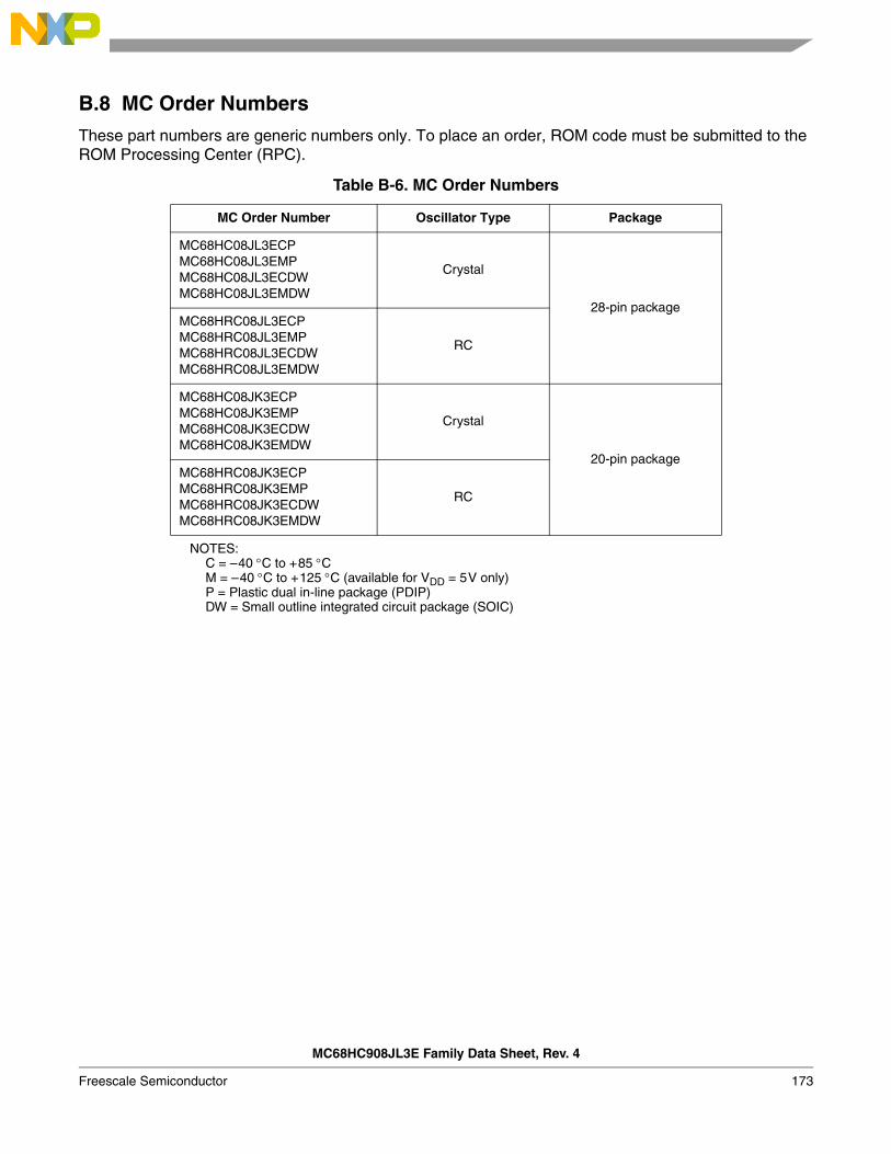
B.8 MC Order Numbers
These part numbers are generic numbers only. To place an order, ROM code must be submitted to the ROM Processing Center (RPC).
Table B-6. MC Order Numbers
MC Order Number Oscillator Type Package
MC68HC08JL3ECPMC68HC08JL3EMPMC68HC08JL3ECDWMC68HC08JL3EMDW
Crystal
28-pin packageMC68HRC08JL3ECPMC68HRC08JL3EMPMC68HRC08JL3ECDWMC68HRC08JL3EMDW
RC
MC68HC08JK3ECPMC68HC08JK3EMPMC68HC08JK3ECDWMC68HC08JK3EMDW
Crystal
20-pin packageMC68HRC08JK3ECPMC68HRC08JK3EMPMC68HRC08JK3ECDWMC68HRC08JK3EMDW
RC
NOTES:C = –40 °C to +85 °CM = –40 °C to +125 °C (available for VDD = 5V only)P = Plastic dual in-line package (PDIP)DW = Small outline integrated circuit package (SOIC)
MC68HC908JL3E Family Data Sheet, Rev. 4
Freescale Semiconductor 173

MC68HC908JL3E Family Data Sheet, Rev. 4
174 Freescale Semiconductor

Appendix C MC68HC908KL3E/KK3E
C.1 Introduction
This appendix introduces two devices, that are ADC-less versions of MC68HC908JL3E/JK3E:• MC68HC908KL3E• MC68HC908KK3E
The entire data book applies to these devices, with exceptions outlined in this appendix.
C.2 MCU Block Diagram
Figure C-1 shows the block diagram of the MC68HC908KL3E/KK3E.
C.3 Pin Assignments
Figure C-2 and Figure C-3 show the pin assignments for the MC68HC908KL3E/KK3E.
Table C-1. Summary of MC68HC908KL3E/KK3E and MC68HC908JL3E Differences
MC68HC908KL3E/KK3E MC68HC908JL3E
Analog-to-Digital Converter (ADC) — 12-channel, 8-bit.
Registers at: $003C, $003E, and $003E
Not used; locations are reserved.
ADC registers.
Interrupt Vector at: $FFDE and $FFDF
Not used. ADC interrupt vector.
Available Packages
20-pin PDIP (MC68HC908KK3E)20-pin SOIC (MC68HC908KK3E)28-pin PDIP28-pin SOIC—
20-pin PDIP (MC68HC908JK3E)20-pin SOIC (MC68HC908JK3E)28-pin PDIP28-pin SOIC48-pin LQFP
MC68HC908JL3E Family Data Sheet, Rev. 4
Freescale Semiconductor 175
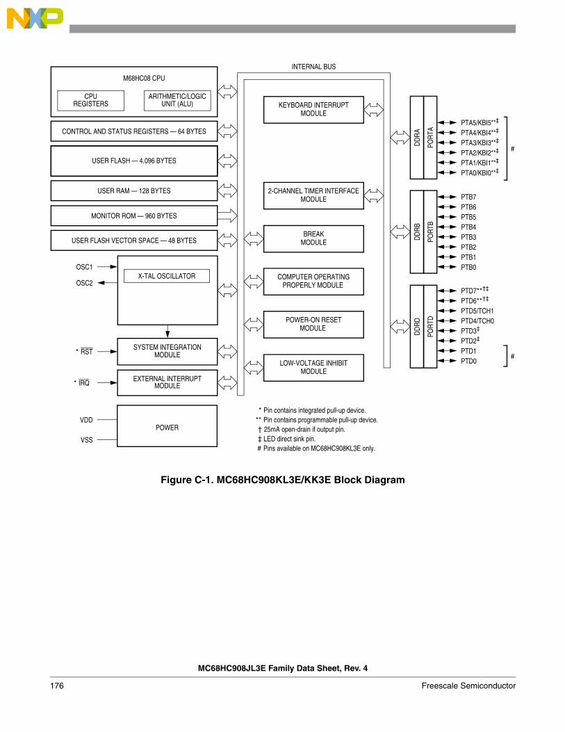
Figure C-1. MC68HC908KL3E/KK3E Block Diagram
SYSTEM INTEGRATIONMODULE
ARITHMETIC/LOGICUNIT (ALU)
CPUREGISTERS
M68HC08 CPU
CONTROL AND STATUS REGISTERS — 64 BYTES
USER FLASH — 4,096 BYTES
USER RAM — 128 BYTES
MONITOR ROM — 960 BYTES
USER FLASH VECTOR SPACE — 48 BYTES
EXTERNAL INTERRUPTMODULE
INTERNAL BUS
* RST
* IRQ
POWER
VSS
2-CHANNEL TIMER INTERFACEMODULE
KEYBOARD INTERRUPTMODULE
VDDD
DR
B
POR
TB
PTB7PTB6PTB5PTB4PTB3PTB2PTB1PTB0
DD
RA
POR
TA
PTA5/KBI5**‡
PTA4/KBI4**‡
PTA3/KBI3**‡
PTA2/KBI2**‡
PTA1/KBI1**‡
PTA0/KBI0**‡
LOW-VOLTAGE INHIBITMODULE
* Pin contains integrated pull-up device.** Pin contains programmable pull-up device.† 25mA open-drain if output pin.‡ LED direct sink pin.
OSC1
OSC2X-TAL OSCILLATOR
DD
RD
POR
TD
PTD7**†‡
PTD6**†‡
PTD5/TCH1PTD4/TCH0PTD3‡
PTD2‡
PTD1PTD0
COMPUTER OPERATINGPROPERLY MODULE
POWER-ON RESETMODULE
BREAKMODULE
#
#
# Pins available on MC68HC908KL3E only.
MC68HC908JL3E Family Data Sheet, Rev. 4
176 Freescale Semiconductor

Figure C-2. 28-Pin PDIP/SOIC Pin Assignment
Figure C-3. 20-Pin PDIP/SOIC Pin Assignment
1
2
3
4
5
6
7
28
27
26
25
24
23
22
21
20
19
18
12
13
14
17
16
15
8
9
10
11
RST
PTA5/KBI5
PTD4/TCH0
PTD5/TCH1
PTD2
PTA4
PTD3
PTB0
PTB1
PTD1
PTB2
PTB3
PTD0
PTB4
IRQ
PTA0/KBI0
VSS
OSC1
OSC2
PTA1/KBI1
VDD
PTA2/KBI2
PTA3/KBI3
PTB7
PTB6
PTB5
PTD7
PTD6
MC68HC908KL3E
1
2
3
4
5
6
7
20
19
18
17
16
15
14
13
12
11
8
9
10
RST
PTD4/TCH0
PTD5/TCH1
PTD2
PTD3
PTB0
PTB1
PTB2
PTB3
PTB4
IRQ
VSS
OSC1
OSC2
VDD
PTB7
PTB6
PTB5
PTD7
PTD6
Pins not available on 20-pin packages
PTA0/KBI0 PTD0
PTA1/KBI1 PTD1
PTA2/KBI2
PTA3/KBI3
PTA4/KBI4
PTA5/KBI5
Internal pads are unconnected.
MC68HC908KK3E
MC68HC908JL3E Family Data Sheet, Rev. 4
Freescale Semiconductor 177

C.4 Reserved Registers
The following registers are reserved location on the MC68HC908KL3E/KK3E.
C.5 Reserved Vectors
The following vectors are reserved interrupt vectors on the MC68HC908KL3E/KK3E.
C.6 Order Numbers
Addr. Register Name Bit 7 6 5 4 3 2 1 Bit 0
$003C Reserved
Read:R R R R R R R R
Write:
Reset:
$003D Reserved
Read:R R R R R R R R
Write:
Reset:
$003E Reserved
Read:R R R R R R R R
Write:
Reset:
Figure C-4. Reserved Registers
Table C-2. Reserved Vectors
Vector Priority INT Flag Address Vector
— IF15$FFDE Reserved
$FFDF Reserved
Table C-3. MC68HC908KL3E/KK3E Order Numbers
MC order number PackageOperating
TemperatureOperating
VDDOSC Flash Memory
MC68HC908KL3ECP 28-pin PDIP
–40 to +85 °C 3V, 5V XTAL 4096 BytesMC68HC908KL3ECDW 28-pin SOIC
MC68HC908KK3ECP 20-pin PDIP
MC68HC908KK3ECDW 20-pin SOIC
MC68HC908JL3E Family Data Sheet, Rev. 4
178 Freescale Semiconductor


How to Reach Us:
Home Page:www.freescale.com
E-mail:[email protected]
USA/Europe or Locations Not Listed:Freescale SemiconductorTechnical Information Center, CH3701300 N. Alma School RoadChandler, Arizona 85224+1-800-521-6274 or [email protected]
Europe, Middle East, and Africa:Freescale Halbleiter Deutschland GmbHTechnical Information CenterSchatzbogen 781829 Muenchen, Germany+44 1296 380 456 (English)+46 8 52200080 (English)+49 89 92103 559 (German)+33 1 69 35 48 48 (French)[email protected]
Japan:Freescale Semiconductor Japan Ltd.HeadquartersARCO Tower 15F1-8-1, Shimo-Meguro, Meguro-ku,Tokyo 153-0064Japan0120 191014 or +81 3 5437 [email protected]
Asia/Pacific:Freescale Semiconductor Hong Kong Ltd.Technical Information Center2 Dai King StreetTai Po Industrial EstateTai Po, N.T., Hong Kong+800 2666 [email protected]
For Literature Requests Only:Freescale Semiconductor Literature Distribution CenterP.O. Box 5405Denver, Colorado 802171-800-441-2447 or 303-675-2140Fax: [email protected]
RoHS-compliant and/or Pb-free versions of Freescale products have the functionality and electrical characteristics of their non-RoHS-compliant and/or non-Pb-free counterparts. For further information, see http://www.freescale.com or contact your Freescale sales representative.
For information on Freescale’s Environmental Products program, go to http://www.freescale.com/epp.
Information in this document is provided solely to enable system and software implementers to use Freescale Semiconductor products. There are no express or implied copyright licenses granted hereunder to design or fabricate any integrated circuits or integrated circuits based on the information in this document.
Freescale Semiconductor reserves the right to make changes without further notice to any products herein. Freescale Semiconductor makes no warranty, representation or guarantee regarding the suitability of its products for any particular purpose, nor does Freescale Semiconductor assume any liability arising out of the application or use of any product or circuit, and specifically disclaims any and all liability, including without limitation consequential or incidental damages. “Typical” parameters that may be provided in Freescale Semiconductor data sheets and/or specifications can and do vary in different applications and actual performance may vary over time. All operating parameters, including “Typicals”, must be validated for each customer application by customer’s technical experts. Freescale Semiconductor does not convey any license under its patent rights nor the rights of others. Freescale Semiconductor products are not designed, intended, or authorized for use as components in systems intended for surgical implant into the body, or other applications intended to support or sustain life, or for any other application in which the failure of the Freescale Semiconductor product could create a situation where personal injury or death may occur. Should Buyer purchase or use Freescale Semiconductor products for any such unintended or unauthorized application, Buyer shall indemnify and hold Freescale Semiconductor and its officers, employees, subsidiaries, affiliates, and distributors harmless against all claims, costs, damages, and expenses, and reasonable attorney fees arising out of, directly or indirectly, any claim of personal injury or death associated with such unintended or unauthorized use, even if such claim alleges that Freescale Semiconductor was negligent regarding the design or manufacture of the part.
Freescale™ and the Freescale logo are trademarks of Freescale Semiconductor, Inc.All other product or service names are the property of their respective owners.
© Freescale Semiconductor, Inc. 2005. All rights reserved.
MC68HC908JL3ERev. 4, 10/2006