mc96f1206 user’s manual
TRANSCRIPT

Global Top Smart MCU Innovator, ABOV Semiconductor
www.abovsemi.com
MC96F1206 User’s Manual
CMOS single-chip 8-bit MCU with 12-bit ADC and LDO
Version 1.21
Introduction
This user’s manual targets application developers who use MC96F1206 for their specific needs. It
provides complete information of how to use MC96F1206 device. Standard functions and blocks
including corresponding register information of MC96F1206.
MC96F1206 incorporates followings to offer highly flexible and cost effective solutions: 6Kbytes of
FLASH, 256bytes of IRAM, general purpose I/O, basic interval timer,watchdog timer, 16-bit
timer/counter, 16-bit PWM output, 12-bit A/D converter, on-chip POR, LVR, LVI, on-chip oscillator and
clock circuitry. We introduces rich features such as excellent noise immunity, code optimization,
costeffectiveness, and so on.
Figure 1. MC96F1206 Block Diagram
Reference documents
MC96F1206 programming tools and manuals released by ABOV: They are available at ABOV
website, www.abovsemi.com
SDK-51 User’s guide (System Design Kit) released by Intel in 1982: It contains all of
components of a single-board computer based on Intel’s 8051 single-chip microcomputer
Information on Mentor Graphics 8051 microcontroller: The technical document is provided at
Mentor website: https://www.mentor.com/products/ip/peripheral/microcontroller/

Contents MC96F1206 User’s manual
2
Contents
Device overview ............................................................................................................... 9
Block diagram ................................................................................................................ 11
Pinouts ........................................................................................................................... 12
Pin description ................................................................................................................ 14
GPIO port structure ........................................................................................................ 16
External interrupt I/O port structure ................................................................................ 17
Program memory ........................................................................................................... 18
Internal data memory ..................................................................................................... 19
Extended SFR area........................................................................................................ 21
SFR map ........................................................................................................................ 21
4.4.1 SFR map summary ................................................................................................ 22
4.4.2 SFR map ................................................................................................................ 22
4.4.3 8051 Compiler Compatible SFR map .................................................................... 28
I/O ports ......................................................................................................................... 30
Port registers .................................................................................................................. 30
5.2.1 Data register (Px) ................................................................................................... 30
5.2.2 Direction register (PxIO) ......................................................................................... 30
5.2.3 Pull-up register selection register (PxPU) .............................................................. 30
5.2.4 Open-drain selection register (PxOD) .................................................................... 30
5.2.5 Port function selection register (PSR0,PSR2,PSR3) ............................................. 30
5.2.6 Pin Change Interrupt Enable Register (PCI) .......................................................... 31
5.2.7 Register map .......................................................................................................... 31
Port P0 ........................................................................................................................... 31
5.3.1 Port description of P0 ............................................................................................. 31
5.3.2 Register description of P0 ...................................................................................... 32
Port P1 ........................................................................................................................... 33
5.4.1 Port description of P1 ............................................................................................. 33
5.4.2 Register description of P1 ...................................................................................... 33
Port P2 ........................................................................................................................... 34
5.5.1 Port description of P2 ............................................................................................. 34
5.5.2 Register description of P2 ...................................................................................... 34
External interrupt ............................................................................................................ 38
Pin Change Interrupt ...................................................................................................... 38
Interrupt controller block diagram .................................................................................. 40
Interrupt vector table ...................................................................................................... 40
Interrupt sequence ......................................................................................................... 41
Effective timing after controlling interrupt bit .................................................................. 44
Multi interrupt ................................................................................................................. 44
Interrupt enable accept timing ........................................................................................ 45
Interrupt Service Routine Address ................................................................................. 46
Saving/ restore general-purpose registers ..................................................................... 46
Interrupt timing ............................................................................................................... 47
MC96F1206 User’s manual Contents
3
Interrupt register ............................................................................................................. 48
6.12.1 Interrupt Enable registers (IE, IE1) ......................................................................... 48
6.12.2 Interrupt Priority registers (IP, IP1) ......................................................................... 48
6.12.3 External Interrupt Flag register (EIFLAG) .............................................................. 48
6.12.4 External Interrupt Polarity registers (EIPOL0, EIPOL1) ......................................... 49
6.12.5 Register map .......................................................................................................... 49
6.12.6 Interrupt register description ................................................................................... 49
Block diagram ................................................................................................................ 53
Register map .................................................................................................................. 53
Register description ....................................................................................................... 53
Block diagram ................................................................................................................ 55
Register map .................................................................................................................. 55
Register description ....................................................................................................... 55
Block diagram ................................................................................................................ 57
WDT interrupt timing waveform ..................................................................................... 57
Register map .................................................................................................................. 58
16-bit timer/ counter mode ............................................................................................. 60
16-bit capture mode ....................................................................................................... 61
PWM Mode .................................................................................................................... 64
Timer Data and Period/Duty Write ................................................................................. 65
Register map .................................................................................................................. 66
Register description for Timer/Counter x ....................................................................... 67
Block diagram ................................................................................................................ 72
ADC Operation ............................................................................................................... 73
Register map .................................................................................................................. 75
Register Description for ADC ......................................................................................... 75
Peripheral Operation in IDLE/STOP Mode .................................................................... 78
IDLE mode ..................................................................................................................... 79
STOP mode ................................................................................................................... 79
Release operation of STOP1,2 mode ............................................................................ 80
Register Map and Register Description for Power Down Operation ............................. 81
Register description ....................................................................................................... 81
Reset block diagram ...................................................................................................... 82
Power on Reset .............................................................................................................. 82
External RESETB input .................................................................................................. 86
Low Voltage Indicator Processor ................................................................................... 87
13.4.1 Block diagram ......................................................................................................... 87
13.4.2 Internal reset and LVD reset in timing diagram ...................................................... 88
Register map .................................................................................................................. 88
Register description ....................................................................................................... 88
Flash program ROM structure ....................................................................................... 91
Register map .................................................................................................................. 92

Contents MC96F1206 User’s manual
4
Register description ....................................................................................................... 92
Serial In-System Program (ISP) mode........................................................................... 95
14.4.1 Flash operation ....................................................................................................... 95
14.4.2 Flash Read ............................................................................................................. 97
14.4.3 Enable program mode ............................................................................................ 97
14.4.4 Flash write mode .................................................................................................... 97
14.4.5 Flash page erase mode .......................................................................................... 98
14.4.6 Flash bulk erase mode ........................................................................................... 98
14.4.7 Flash OTP area read mode .................................................................................... 98
14.4.8 Flash OTP area write mode ................................................................................... 99
14.4.9 Flash OTP area erase mode .................................................................................. 99
14.4.10 Flash program verify mode ..................................................................................... 99
14.4.11 Flash program verify mode ..................................................................................... 99
14.4.12 OTP program verify mode .................................................................................... 100
14.4.13 Flash erase verify mode ....................................................................................... 100
14.4.14 Flash page buffer read ......................................................................................... 100
Summary of Flash Program/Erase Mode..................................................................... 100
Security ........................................................................................................................ 100
Absolute maximum ratings ........................................................................................... 102
Recommended Operating Conditions .......................................................................... 102
A/D Converter Characteristics ..................................................................................... 103
Low Drop Out Characteristics ...................................................................................... 103
Power-On Reset Characteristics .................................................................................. 103
Low Voltage Reset and Low Voltage Indicator Characteristics ................................... 104
Internal RC Oscillator Characteristics .......................................................................... 104
Internal WDT Oscillator Characteristics ....................................................................... 105
DC Characteristics ....................................................................................................... 105
AC Characteristics ....................................................................................................... 106
Operating Voltage Range ............................................................................................ 107
Typical Characteristics ................................................................................................. 107
Recommended Application Circuit ............................................................................... 108
Compiler ....................................................................................................................... 110
OCD (On-Chip Debugger) emulator and debugger ..................................................... 110
Programmer ................................................................................................................. 111
MTP programming ....................................................................................................... 112
Circuit design guide...................................................................................................... 113
16.5.1 On-Chip Debug system ........................................................................................ 115
16.5.2 Two-pin external interface .................................................................................... 116
16.5.3 Connection of transmission .................................................................................. 119
A. Configure option ...................................................................................................................... 124
B. Instruction table ....................................................................................................................... 125
C. Flash protection for invalid erase/ write .................................................................................. 131
How to protect the flash ........................................................................................................... 131
Protection flow description ...................................................................................................... 132
Other protection by the configure options ............................................................................... 134

MC96F1206 User’s manual Contents
5

List of figures MC96F1206 User’s manual
6
List of figures Figure 1. MC96F1206 Block Diagram ..................................................................................................... 1
Figure 2. MC96F1206 Block Diagram ................................................................................................... 11
Figure 3. MC96F1206AEN 16 SOPN Pinouts ...................................................................................... 12
Figure 4. MC96F1206 20TSSOP assignment ...................................................................................... 13
Figure 5. MC96F1206 16SOPN assignment ........................................................................................ 13
Figure 6. General Purpose I/O Port Structure ....................................................................................... 16
Figure 7. External Interrupt I/O Port Structure ...................................................................................... 17
Figure 8. Program Memory ................................................................................................................... 19
Figure 9. Internal Data Memory Map .................................................................................................... 20
Figure 10. Lower 128 bytes Internal RAM ............................................................................................ 21
Figure 11. Interrupt Group Priority Level ............................................................................................... 38
Figure 12. External Interrupt Description .............................................................................................. 39
Figure 13. PCI Interrupt Description ..................................................................................................... 39
Figure 14. Interrupt Controller Block Diagram ...................................................................................... 40
Figure 15. Interrupt Sequence Flow ...................................................................................................... 43
Figure 16. Case A: Effective Timing of Interrupt Enable Register ......................................................... 44
Figure 17. Case B: Effective Timing of Interrupt Flag Register ............................................................. 44
Figure 18. Effective Timing of Multi Interrupt ........................................................................................ 45
Figure 19. Interrupt Response Timing Diagram .................................................................................... 46
Figure 20. Correspondence between Vector Table Address and ISR Entry Address ........................... 46
Figure 21. Saving and Restore Process Diagram and Example Code ................................................. 47
Figure 22. Timing Chart of Interrupt Acceptance and Interrupt Return Instruction ............................... 48
Figure 23. Clock Generator in Block Diagram ...................................................................................... 53
Figure 24. Basic Interval Timer in Block Diagram ................................................................................. 55
Figure 25. Watchdog Timer in Block Diagram ...................................................................................... 57
Figure 26. Watchdog Timer Interrupt Timing Waveform ....................................................................... 58
Figure 27. 16-bit Timer/ Counter Mode of TIMER 0/1 ........................................................................... 61
Figure 28. 16-bit Timer/ Counter 0/1 Interrupt Example ....................................................................... 61
Figure 29. 16-bit Capture Mode of TIMER 0/1 ...................................................................................... 62
Figure 30. Input Capture Mode Operation of TIMER 0/1 ...................................................................... 63
Figure 31. Express Timer Overflow in Capture Mode ........................................................................... 63
Figure 32. PWMx Mode Block Diagram ................................................................................................ 64
Figure 33. Example of PWM at 8MHz ................................................................................................... 65
Figure 34. Example of PWM at 8MHz(Duty=Period) ............................................................................ 65
Figure 35. Timer x Compare Data Write ............................................................................................... 66
Figure 36. ADC Block Diagram ............................................................................................................. 72
Figure 37. A/D Analog Input Pin Connecting Capacitor ........................................................................ 72
Figure 38. ADC Operation for Align bit .................................................................................................. 73
Figure 39. Converter Operation Flow .................................................................................................... 74
Figure 40. IDLE Mode Release Timing by External Interrupt ............................................................... 79
Figure 41. STOP Mode Release Timing by External Interrupt .............................................................. 80
Figure 42. STOP Mode Release Flow .................................................................................................. 80
Figure 43. Reset Block Diagram ........................................................................................................... 82
Figure 44. Fast VDD Rising Time ......................................................................................................... 83
Figure 45. Internal Reset Release Timing on Power-Up ...................................................................... 83
Figure 46. Configuration Timing when Power-On ................................................................................. 84
Figure 47. Boot Process Waveform ...................................................................................................... 84
MC96F1206 User’s manual List of figures
7
Figure 48. Timing Diagram after RESET .............................................................................................. 86
Figure 49. Reset noise canceller time diagram..................................................................................... 86
Figure 50. Oscillator Generating Waveform Example ........................................................................... 87
Figure 51. LVI Block Diagram ............................................................................................................... 87
Figure 52. Internal Reset at Power Fail Situation ................................................................................. 88
Figure 53. Flash Memory Map .............................................................................................................. 91
Figure 54.Address configuration of Flash memory ............................................................................... 91
Figure 55.The sequence of page program and erase of Flash memory .............................................. 95
Figure 56. The sequence of bulk erase of Flash memory .................................................................... 96
Figure 57. AC Timing ........................................................................................................................... 106
Figure 58. Operating Voltage Range .................................................................................................. 107
Figure 59. Output Low Voltage(VOL) .................................................................................................. 107
Figure 60. Output High Voltage (VOH1) ............................................................................................. 107
Figure 61. Output High Voltage (VOH2) ............................................................................................. 108
Figure 62.Power Supply Current (RUN, IDLE) ................................................................................... 108
Figure 63. Power Supply Current (STOP1, STOP2) .......................................................................... 108
Figure 64. IRC Tolerance .................................................................................................................... 108
Figure 65. Recommended Power Circuit part when using DC Power. ............................................... 109
Figure 66. OCD and Pin Descriptions ................................................................................................. 110
Figure 67. E-PGM+ (Single Writer) and Pin Descriptions ................................................................... 111
Figure 68. E-Gang4 and E-Gang6 (for Mass Production) .................................................................. 112
Figure 69. PCB Design Guide for On-Board Programming ................................................................ 114
Figure 70. On-Chip Debugging System in Block Diagram .................................................................. 115
Figure 71. 10-bit Transmission Packet ................................................................................................ 116
Figure 72. Data Transfer on Twin Bus ................................................................................................ 117
Figure 73. Bit Transfer on Serial Bus .................................................................................................. 117
Figure 74. Start and Stop Condition .................................................................................................... 117
Figure 75. Acknowledge on Serial Bus ............................................................................................... 118
Figure 76. Clock Synchronization during Wait Procedure .................................................................. 118
Figure 77. Connection of Transmission .............................................................................................. 119
Figure 78. 20QFN Package Outline .................................................................................................... 120
Figure 79. 20 TSSOP Package Outline .............................................................................................. 121
Figure 80. 16SOPN Package Outline ................................................................................................. 122
Figure 81. MC96F1206 Device Numbering Nomenclature ................................................................. 123
Figure 82. Flash Protection against Abnormal Operations ................................................................. 131
Figure 83. Flowchart of Flash Protection ............................................................................................ 133

List of tables MC96F1206 User’s manual
8
List of tables Table 1. MC96F1206 Device Features and Peripheral Counts .............................................................. 9
Table 2. 16 SOPN Pin Description ........................................................................................................ 14
Table 3. SFR Map Summary ................................................................................................................. 22
Table 4. SFR Map ................................................................................................................................. 22
Table 5. Port Register Map.................................................................................................................... 31
Table 6. Interrupt Vector Address Table ................................................................................................ 41
Table 7. LJMP Description and Example Code ..................................................................................... 42
Table 8. Interrupt Register Map ............................................................................................................. 49
Table 9. Clock Generator Register Map ................................................................................................ 53
Table 10. Basic Interval Timer Register Map ........................................................................................ 55
Table 11. BIT period Table ..................................................................................................................... 56
Table 12. PWM Frequency vs. Resolution at 16MHz and 32MHz ........................................................ 64
Table 13. TIMER 0 Register Map .......................................................................................................... 66
Table 14. ADC Register Map ................................................................................................................. 75
Table 15. Peripheral Operation during Power Down Mode ................................................................... 78
Table 16. Power-down Operation Register Map ................................................................................... 81
Table 17. Example Code with 3 or more NOP Instructions ................................................................... 81
Table 18. Reset Value and the Relevant On Chip Hardware ................................................................ 82
Table 19. Boot Process Description ...................................................................................................... 85
Table 20. Reset Operation Register Map .............................................................................................. 88
Table 21. Flash Memory Register Map ................................................................................................. 92
Table 22. Program/erase Time .............................................................................................................. 94
Table 23.Operation Mode .................................................................................................................... 100
Table 24.Security policy using lock-bits .............................................................................................. 101
Table 25.Absolute Maximum Ratings .................................................................................................. 102
Table 26.Recommended Operating Conditions .................................................................................. 102
Table 27.Low Drop Out Characteristics .............................................................................................. 103
Table 28.Power-On Reset Characteristics .......................................................................................... 103
Table 29.LVR and LVI Characteristics ................................................................................................. 104
Table 30.Internal RC Oscillator Characteristics .................................................................................. 104
Table 31.Internal WDT Oscillator Characteristics ............................................................................... 105
Table 32.DC Characteristics................................................................................................................ 105
Table 33.AC Characteristics ................................................................................................................ 106
Table 34.Specification of E-Gang4 and E-Gang6 ............................................................................... 112
Table 35. Pins for MTP Programming ................................................................................................. 112
Table 36. Features of OCD ................................................................................................................. 115
Table 37. MC96F1206 Device Ordering Information .......................................................................... 123
Table 38. Instruction Table: Arithmetic................................................................................................. 125
Table 39. Instruction Table: Logical ..................................................................................................... 126
Table 40. Instruction Table: Data Transfer .......................................................................................... 127
Table 41. Instruction Table: Boolean ................................................................................................... 128
Table 42. Instruction Table: Branching ................................................................................................ 129
Table 43. Instruction Table: Miscellaneous ......................................................................................... 129
Table 44. Instruction Table: Additional Instructions ............................................................................. 130

MC96F1206 User’s manual 1. Description
9
Description
The MC96F1206 is an advanced CMOS 8-bit microcontroller with 6 Kbytes of FLASH. This is powerful
microcontroller which provides a highly flexible and cost-effective solution to many embedded control
applications. This provides the following features : 6 Kbytes of FLASH, 256 bytes of SRAM, 16-bit
timer/counter/PWM, Watchdog timer with WDTOSC, 12-bit ADC with LDO, On-chip POR, LVI and LVR,
Internal RC-Oscillator, Internal WDT-Oscillator and clock circuitry. The MC96F1206 also supports
Power saving modes to reduce Power Consumption.
Device overview
Table 1. MC96F1206 Device Features and Peripheral Counts
Peripheral MC96F1206
CPU 8-bit CISC core (M8051, 2 clocks per cycle)
Flash 6 Kbytes with self r/w capability
On chip debug and ISP
Endurance: 10,000 cycles
iRAM 256 bytes
GPIO Normal I/Os
18 ports: P0[7:0], P1[7:0], P2[1:0]
Timer/ counter BIT 8-bit x 1-ch
WDT 8-bit x 1-ch: 8 KHz internal RC oscillator for
WDT
16-bit x 2-ch (T0/T1), 16-bit PWM 2-ch
ADC 12-bit ADC, 15 input channels
Internal 2.5V LDO reference(option)
POR Power on reset(1.1V)
LVR Low voltage reset(1.75V)
Device

1. Description MC96F1206 User’s manual
10
Peripheral MC96F1206
Interrupt sources External interrupts: EINT0/1 (2)
PCI1 (1)
Timer : T0/ T1 (2)
WDT (1)
BIT (1)
ADC (1)
LVI (1)
Internal RC oscillator 32MHz 2.0% (TA = 25)
32MHz 5.0% (TA = -40 to +85)
Power down mode STOP1,STOP2, IDLE
Operating voltage and frequency 2.2V to 5.5V
Voltage dropout converter included for core
Minimum instruction execution time 125ns @16MHz with IRC
Operating temperature -40 to +85
Package type 20QFN, 20TSSOP, 16SOPN
Pb-free package
Device

MC96F1206 User’s manual 1. Description
11
Block diagram
Figure 2 describes MC96F1206 in a block diagram.
IRAM256B
Flash
6KB
On-chip debugIn-system programming
Power controlPower on reset
Low voltage reset
Power down mode
Clock generator
32MHz, IRC OSC
COREM8051
General purpose I/O18 ports normal I/O
Watchdog timer
1 channel, 8-bit
8kHz, internal RC OSC
Basic interval timer1 channel, 8-bit
Timer / Counter2 channels, 16-bit
ADC15 Input channels, 12-bit
Sample and Hold circuit
Figure 2. MC96F1206 Block Diagram
2. Pinouts and pin descriptions MC96F1206 User’s manual
12
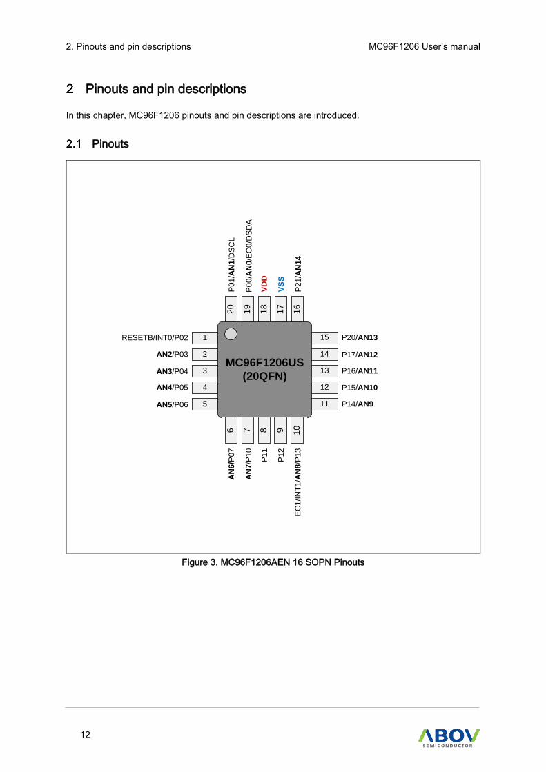
Pinouts and pin descriptions
In this chapter, MC96F1206 pinouts and pin descriptions are introduced.
Pinouts
MC96F1206US
(20QFN)
P0
1/A
N1
/ DS
CL
20
17
18
19
16
6 987 10
AN
6/ P
07
VD
D
VS
S
P2
1/A
N1
4
AN
7/P
10
P1
1
P1
2
EC
1/ IN
T1
/ AN
8/P
13
P17/AN12
15
12
13
14
11
P20/AN13
P15/AN10
P16/AN11
P14/AN9
1
4
3
2
5
AN2/P03
RESETB/INT0/P02
AN4/P05
AN3/P04
AN5/P06
P0
0/A
N0
/ EC
0/ D
SD
A
Figure 3. MC96F1206AEN 16 SOPN Pinouts
MC96F1206 User’s manual 2. Pinouts and pin descriptions
13
MC96F1206R
(20TSSOP)
1
4
3
2
VDD
6
5
VSS
7
10
9
8
20
17
18
19
15
16
14
11
12
13
DSDA/EC0/AN0/P00
RESETB/INT0/P02
DSCL/AN1/P01
AN2/P03
AN3/P04
AN4/P05
AN5/P06
AN6/P07
AN7/P10
P21/AN14
P20/AN13
P17/AN12
P16/AN11
P15/AN10
P14/AN9
P13/AN8/INT1/EC1
P12
P11
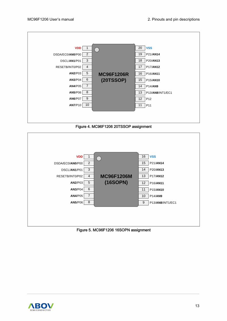
Figure 4. MC96F1206 20TSSOP assignment
MC96F1206M
(16SOPN)
1
4
3
2
VDD
6
5
VSS
7
8
16
13
14
15
11
12
10
9
DSDA/EC0/AN0/P00
RESETB/INT0/P02
DSCL/AN1/P01
AN2/P03
AN3/P04
AN4/P05
AN5/P06
P21/AN14
P20/AN13
P17/AN12
P16/AN11
P15/AN10
P14/AN9
P13/AN8/INT1/EC1
Figure 5. MC96F1206 16SOPN assignment
2. Pinouts and pin descriptions MC96F1206 User’s manual
14
Pin description
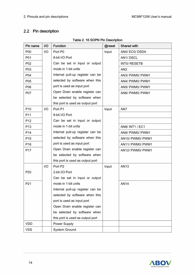
Table 2. 16 SOPN Pin Description
Pin name I/O Function @reset Shared with
P00 I/O Port P0
8-bit I/O Port
Can be set in input or output
mode in 1-bit units
Internal pull-up register can be
selected by software when this
port is used as input port
Open Drain enable register can
be selected by software when
this port is used as output port
Input AN0/ EC0/ DSDA
P01 AN1/ DSCL
P02 INT0/ RESETB
P03 AN2
P04 AN3/ PWM0/ PWM1
P05 AN4/ PWM0/ PWM1
P06 AN5/ PWM0/ PWM1
P07 AN6/ PWM0/ PWM1
P10 I/O
Port P1
8-bit I/O Port
Can be set in input or output
mode in 1-bit units
Internal pull-up register can be
selected by software when this
port is used as input port
Open Drain enable register can
be selected by software when
this port is used as output port
Input AN7
P11
P12
P13 AN8/ INT1 / EC1
P14 AN9/ PWM0/ PWM1
P15 AN10/ PWM0/ PWM1
P16 AN11/ PWM0/ PWM1
P17 AN12/ PWM0/ PWM1
P20
I/O Port P2
2-bit I/O Port
Can be set in input or output
mode in 1-bit units
Internal pull-up register can be
selected by software when this
port is used as input port
Open Drain enable register can
be selected by software when
this port is used as output port
Input AN13
P21 AN14
VDD Power Supply
VSS System Ground

MC96F1206 User’s manual 2. Pinouts and pin descriptions
15
Pin name I/O Function @reset Shared with
EINT0 I/O External interrupt input and
Timer 0 capture input
Input
P02/RESETB
EINT1 I/O External interrupt input and
Timer 1 capture input
P13/AN8/EC1
PWM0O I/O Timer 0 pulse output P0[7:4], P1[7:4], PWM0
PWM1O I/O Timer 1 pulse output P0[7:4], P1[7:4], PWM1
EC0 I/O Timer 0 event count input AN0/DSDA/P00
EC1 I/O Timer 1 event count input AN8/INT1/P13
AN0
I/O
A/D converter analog input
channels Input
P00/EC0/DSDA
AN1 P01/DSCL
AN2 P03
AN3 P04/PWM0/PWM1
AN4 P05/PWM0/PWM1
AN5 P06/PWM0/PWM1
AN6 P07/PWM0/PWM1
AN7 P10
AN8 P13/INT1/EC1
AN9 P14/PWM0/PWM1
AN10 P15/PWM0/PWM1
AN11 P16/PWM0/PWM1
AN12 P17/PWM0/PWM1
AN13 P20
AN14 P21
NOTES:
1. The P02/RESETB pin is configured by the “CONFIGURE OPTION”.
2. If the P00/DSDA and P01/DSCL pins are connected to an emulator during reset or power-on reset,
the pins are automatically configured as the debugger pins.
3. The P00/DSDA and P01/DSCL pins are configured as inputs with an internal pull-up resistor only
during the reset or power-on reset.

3. Port structures MC96F1206 User’s manual
16
Port structures
GPIO port structure
PULL-UP
REGISTERVDD
VDD
PAD
VDD
OPEN DRAIN
REGISTER
DATA
REGISTER
DIRECTION
REGISTER
MUX0
1
MUX
1
0
CMOS or
Schmitt Level
Input
ANALOG CHANNEL
ENABLE
ANALOG INPUT
PORTx INPUT or
SUB-FUNC DATA INPUT
SUB-FUNC DIRECTION
SUB-FUNC ENABLE
SUB-FUNC DATA OUTPUT
Level Shift (ExtVDD to VDC)
Level Shift (VDC to ExtVDD)
Figure 6. General Purpose I/O Port Structure

MC96F1206 User’s manual 3. Port structures
17
External interrupt I/O port structure
PULL-UP
REGISTERVDD
VDD
PAD
VDD
OPEN DRAIN
REGISTER
DATA
REGISTER
DIRECTION
REGISTER
MUX0
1
MUX
1
0
INTERRUPT
ENABLE
EXTERNAL
INTERRUPT
Q D
CPr
VDD
FLAG
CLEAR
POLARITY
REG.
MUX
1
0
DEBOUNCE
ENABLE
Q D
CPr DEBOUNCE
CLK
CMOS or
Schmitt Level
Input
ANALOG CHANNEL
ENABLE
ANALOG INPUT
PORTx INPUT or
SUB-FUNC DATA INPUT
SUB-FUNC DIRECTION
SUB-FUNC ENABLE
SUB-FUNC DATA OUTPUT
Level Shift (ExtVDD to VDC)
Level Shift (VDC to ExtVDD)
Figure 7. External Interrupt I/O Port Structure

4. Memory organization MC96F1206 User’s manual
18
Memory organization
MC96F1206 addresses two separate memory spaces:
Program memory
Data memory
By means of this logical separation of the memory, 8-bit CPU address can access the data memory
more rapidly. 16-bit data memory address is generated through the DPTR register.
MC96F1206 provides on-chip 6 Kbytes of the ISP type flash program memory, which is readable and
writable. Internal data memory (iRAM) is 256 bytes and it includes the stack area.
Program memory
A 16-bit program counter is capable of addressing up to 64 Kbytes, but MC96F1206 has only 6 Kbytes
program memory space. After reset, CPU begins execution from location 0000H. Each interrupt is
assigned to a fixed location of the program memory. The interrupt causes the CPU to jump to that
location, where it commences an execution of a service routine.
For example, an external interrupt 1 is assigned to location 000BH. If the external interrupt 1 is going
to be used, its service routine must begin at location 000BH. If the interrupt is not going to be used, its
service location is available as general purpose program memory. If an interrupt service routine is short
enough (frequent cases with a control application), the service routine can reside entirely within an 8
byte interval.
A longer service routine can use a jump instruction to skip over subsequent interrupt locations, if other
interrupts are in use. Figure 8 shows a map of the lower part of the program memory.

MC96F1206 User’s manual 4. Memory organization
19
Program Memory Areas
6Kbytes
17FFH
0000H
Configuration Areas 0
32bytes0000H
001FH
Configuration Areas 1
32bytes0020H
003FH
Configuration Areas 2
32bytes0040H
005FH
Configuration Areas 3
32bytes0060H
007FH
Figure 8. Program Memory
More detailed description of program memory is introduced in chapter 14. Flash memory later part in
this document.
Internal data memory
Internal data memory is divided into three spaces as shown in figure 9. Those three spaces are
generally called as,
Lower 128 bytes
Upper 128 bytes
Special Function Registers (SFR space)
Internal data memory addresses are always one byte wide, which implies an address space of 256
bytes.
In fact, the addressing modes of the internal data memory can accommodate up to 384 bytes by using
a simple trick. Direct addresses higher than 7FH access one memory space and indirect addresses
higher than 7FH access a different memory space. By means of this method, the upper 128 bytes and
SFR space can occupy the same block of addresses, 80H through FFH, although they are physically
separate entities as shown in figure 3.

4. Memory organization MC96F1206 User’s manual
20
Figure 9. Internal Data Memory Map
The lower 128 bytes of RAM are present in all 8051 devices as mapped in figure 8. The lowest 32 bytes
are grouped into 4 banks of 8 registers. Program instructions call out these registers as R0 through R7.
Two bits in the Program Status Word select which register bank is in use. This allows more efficient use
of code space, since register instructions are shorter than instructions that use direct addressing.
The next 16 bytes above the register banks form a block of bit-addressable memory space. The 8051
instruction set includes a wide selection of single-bit instructions, and the 128 bits in this area can be
directly addressed by these instructions. The bit addresses in this area are 00H through 7FH.
Entire bytes in the lower 128 bytes can be accessed by either direct or indirect addressing, while the
upper 128 bytes RAM can only be accessed by indirect addressing. These spaces are used for data
RAM and stack.

MC96F1206 User’s manual 4. Memory organization
21
Bit Addressable
7FH
General Purpose
Register
30H
80 Bytes
2FH
20H
16 Bytes
(128bits)
Register Bank 3
(8 Bytes)
1FH
18H
8 Bytes
Register Bank 2
(8 Bytes)
17H
10H
8 Bytes
Register Bank 1
(8 Bytes)
0FH
08H
8 Bytes
Register Bank 0
(8 Bytes)
07H
00H
8 Bytes
R7
R6
R5
R4
R3
R2
R1
R0
7F 7E 7D 7C 7B 7A 79 78
77 76 75 74 73 72 71 70
6F 6E 6D 6C 6B 6A 69 68
67 66 65 64 63 62 61 60
5F 5E 5D 5C 5B 5A 59 58
57 56 55 54 53 52 51 50
4F 4E 4D 4C 4B 4A 49 48
47 46 45 44 43 42 41 40
3F 3E 3D 3C 3B 3A 39 38
37 36 35 34 33 32 31 30
2F 2E 2D 2C 2B 2A 29 28
27 26 25 24 23 22 21 20
1F 1E 1D 1C 1B 1A 19 18
17 16 15 14 13 12 11 10
0F 0E 0D 0C 0B 0A 09 08
07 06 05 04 03 02 01 00
Figure 10. Lower 128 bytes Internal RAM
Extended SFR area
Extended SFR area has no relation with RAM nor FLASH. This area can be read or written to by using
SFR in 8-bit unit but XSFR is not used in MC96F1206.
SFR map
In this section, information of SFR map and map summaries are introduced through tables 3 to 6.
4. Memory organization MC96F1206 User’s manual
22
4.4.1 SFR map summary
Table 3. SFR Map Summary
00H/8HNOTE 01H/9H 02H/0AH 03H/0BH 04H/0CH 05H/0DH 06H/0EH 07H/0FH
0F8H IP1
0F0H B FEARL FEARM FEARH
0E8H FEMR FECR FESR FETCR
0E0H ACC P2PU
0D8H P1PU PSR0 PSR2 PSR3 PSRPWM
0D0H PSW P0PU
0C8H
0C0H P2OD
0B8H IP P1OD T1CR T1CR1
PWM1DRL
C1R1L /
T1L
PWM1DRH
CDR1H /
T1H
PWM1PRL
T1DRL
PWM1PRH
T1DRH
0B0H P0OD T0CR T0CR1
PWM0DRL
CDR0L /
T0L
PWM0DRH
CDR0H /
T0H
PWM0PRL
T0DRL
PWM0PRH
T0DRH
0A8H IE IE1
0A0H LDOCR EO EIENAB EIFLAG EIEDGE EIPOLA EIBOTH
98H P2IO PCI1
90H P2 P1IO ADCM1 ADCM ADCRL ADCRH
88H P1 P0IO SCCR BCCR BITR WDTMR WDTR
/WDTCR LVIR
80H P0 SP DPL DPH DPL1 DPH1 RSFR PCON
NOTE: Registers 00H/8H are bit-addressable.
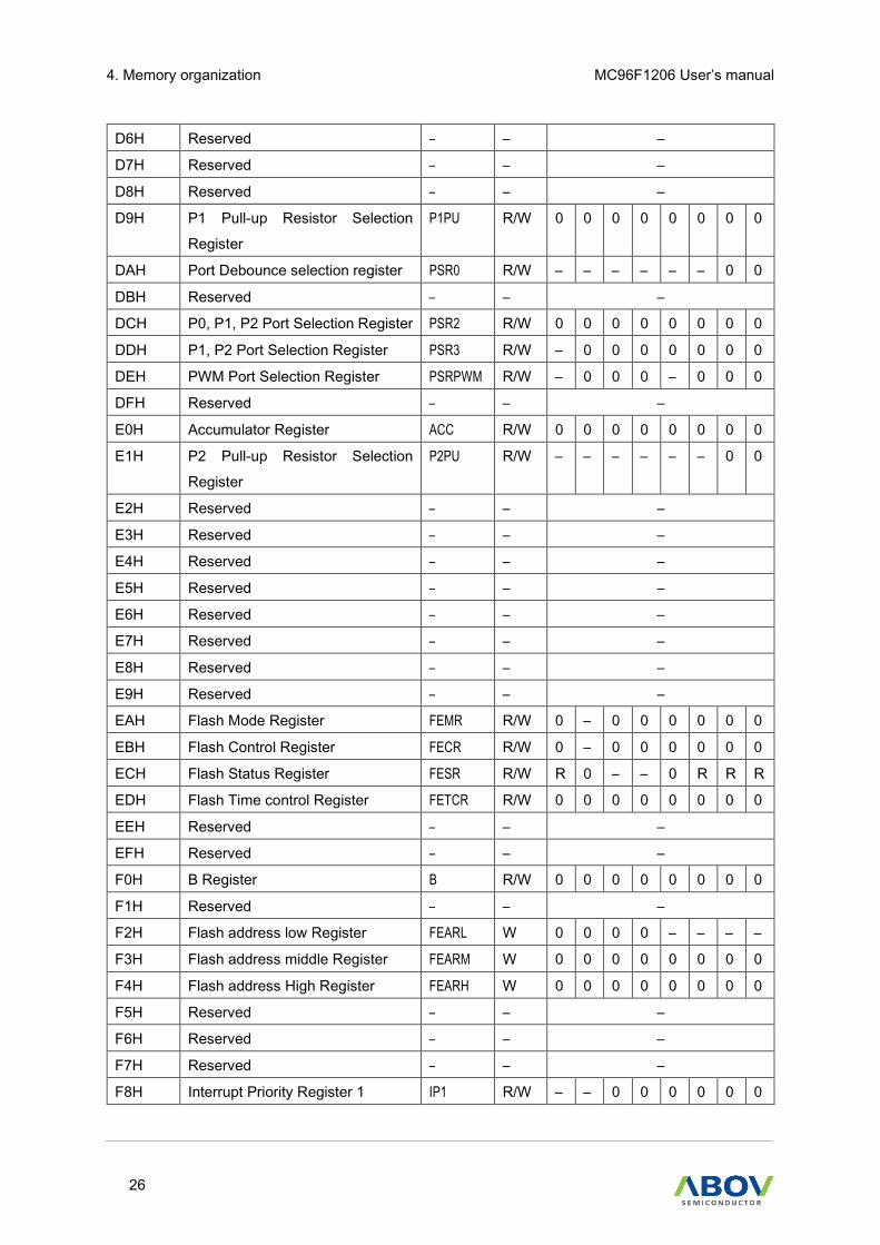
4.4.2 SFR map
Table 4. SFR Map
Address Function Symbol R/W @ Reset
7 6 5 4 3 2 1 0
80H P0 Data Register P0 R/W 0 0 0 0 0 0 0 0
81H Stack Pointer SP R/W 0 0 0 0 0 1 1 1
82H Data Pointer Register Low DPL R/W 0 0 0 0 0 0 0 0
83H Data Pointer Register High DPH R/W 0 0 0 0 0 0 0 0
84H Data Pointer Register Low 1 DPL1 R/W 0 0 0 0 0 0 0 0
85H Data Pointer Register High 1 DPH1 R/W 0 0 0 0 0 0 0 0
86H Reset Source Flag Register RSFR R/W 1 1 0 0 0 1 - -
– Reserved M8051 compatible

MC96F1206 User’s manual 4. Memory organization
23
87H Power Control Register PCON R/W – – – – – – 0 0
88H P1 Data Register P1 R/W – – 0 0 0 0 0 0
89H P0 Direction Register P0IO R/W 0 0 0 0 0 0 0 0
8AH System and Clock Control
Register SCCR R/W 0 0 0 0 – – 0
8BH BIT Clock Control Register BCCR R/W 0 R R 0 0 1 1 0
8CH Basic Interval Timer Register BITR R 0 0 0 0 0 0 0 0
8DH Watch Dog Timer Mode Register WDTMR R/W 0 0 0 – – – – 0
8EH Watch Dog Timer Register WDTR W 1 1 1 1 1 1 1 1
8EH Watch Dog Timer Counter
Register: Read Case WDTCR R X X X X X X X X
8FH LVI Control Register LVIR R/W - 1 - - - 0 0 0
90H P2 Data Register P2 R/W 0 0 0 0 0 0 0 0
91H P1 Direction Register P1IO R/W 0 0 0 0 0 0 0 0
92H Reserved - R/W -
93H Reserved - R/W -
94H A/D Converter Mode Register ADCM1 R/W 1 0 0 1 - 1 0 0
95H A/D Converter Mode Register ADCM R/W 1 0 0 0 1 1 1 1
96H A/D Converter Result Low
Register ADCRL R X X X X X X X X
97H A/D Converter Result High
Register ADCRH R X X X X X X X X
98H Reserved – – –
99H P2 Direction Register P2IO R/W – – – – – – 0 0
9AH Reserved – – –
9BH Reserved – – –
9CH Reserved – – –
9DH Reserved – – –
9EH Reserved – – –
9FH Reserved – – –
A0H Reserved – – –
A1H Reserved – – –
A2H Extended Operation Register EO R/W – – – 0 – 0 0 0
A3H External Interrupt Enable Register EIENAB R/W – – – – – – 0 0
A4H External Interrupt Flag Register EIFLAG R/W – – – – – 0 0 0
A5H External Interrupt Edge Register EIEDGE R/W – – – – – – 0 0
A6H External Interrupt Polarity Register EIPOLA R/W – – – – – – 0 0
A7H External Interrupt Both Edge EIBOTH R/W – – – – – – 0 0

4. Memory organization MC96F1206 User’s manual
24
Enable Register
A8H Interrupt Enable Register IE R/W 0 – 0 0 0 0 0 0
A9H Interrupt Enable Register 1 IE1 R/W – – – – 0 0 – 0
AAH Reserved – – –
ABH Reserved – – –
ACH Reserved – – –
ADH Reserved – – –
AEH Reserved – – –
AFH Reserved – – –
B0H Reserved – – –
B1H P0 Open-drain Selection Register P0OD R/W 0 0 0 0 0 0 0 0
B2H Timer 0 Control Register T0CR R/W 0 0 0 0 0 0 0 0
B3H Timer 0 Control Register1 T0CR1 R/W – 0 0 0 0 0 0 0
B4H PWM 0 Duty Register Low, Write
Case
PWM0DR
L
W 0 0 0 0 0 0 0 0
B4H Timer 0 Register Low, Read Case T0L R 0 0 0 0 0 0 0 0
B4H Capture 0 Data Register Low,
Read Case
CDR0L R 0 0 0 0 0 0 0 0
B5H PWM0 Duty Register High, Write
Case
PWM0DR
H
W 0 0 0 0 0 0 0 0
B5H Timer 0 Register High, Read Case T0H R 0 0 0 0 0 0 0 0
B5H Capture 0 Data High Register,
Read Case
CDR0H R 0 0 0 0 0 0 0 0
B6H PWM 0 Period Register Low, Write
Case
PWM0PR
L
W 0 0 0 0 0 0 0 0
B6H Timer 0 Data Register Low, Write
Case
T0DRL W 0 0 0 0 0 0 0 0
B7H PWM 0 Period Register Low, Write
Case
PWM0PR
H
W 0 0 0 0 0 0 0 0
B7H Timer 0 Data Register High, Write
Case
T0DRH W 0 0 0 0 0 0 0 0
B8H Interrupt Priority Register IP R/W – – 0 0 0 0 0 0
B9H P1 Open-drain Selection Register P1OD R/W 0 0 0 0 0 0 0 0
BAH Timer 1 Control Register T1CR R/W 0 0 0 0 0 0 0 0
BBH Timer 1 Control Register1 T1CR1 R/W - 0 0 0 0 0 0 0
BCH PWM 1 Duty Register Low, Write
Case
PWM1DR
L
W 0 0 0 0 0 0 0 0
BCH Timer 1 Register Low, Read Case T1L R 0 0 0 0 0 0 0 0

MC96F1206 User’s manual 4. Memory organization
25
BCH Capture 1 Data Register Low,
Read Case
CDR1L R 0 0 0 0 0 0 0 0
BDH PWM 1 Duty Register High, Write
Case
PWM1DR
H
W 0 0 0 0 0 0 0 0
BDH Timer 0 Register High, Read Case T1H R 0 0 0 0 0 0 0 0
BDH Capture 1 Data High Register,
Read Case
CDR1H R 0 0 0 0 0 0 0 0
BEH PWM 1 Period Register Low, Write
Case
PWM1PR
L
W 0 0 0 0 0 0 0 0
BEH Timer 1 Data Register Low, Write
Case
T1DRL W 0 0 0 0 0 0 0 0
BFH PWM 1 Period Register Low, Write
Case
PWM1PR
H
W 0 0 0 0 0 0 0 0
BFH Timer 1 Data Register High, Write
Case
T1DRH W 0 0 0 0 0 0 0 0
C0H Reserved – – –
C1H P2OD R/W – – – – – – 0 0
C2H Reserved – – –
C3H Reserved – – –
C4H Reserved – – –
C5H Reserved – – –
C6H Reserved – – –
C7H Reserved – – –
C8H Reserved – – –
C9H Reserved – – –
CAH Reserved – – –
CBH Reserved – – –
CCH Reserved – – –
CDH Reserved – – –
CEH Reserved – – –
CFH Reserved – – –
D0H Program Status Word Register PSW R/W 0 0 0 0 0 0 0 0
D1H P0 Pull-up Resistor Selection
Register
P0PU R/W 0 0 0 0 0 0 0 0
D2H Reserved – – –
D3H Reserved – – –
D4H Reserved – – –
D5H Reserved – – –
4. Memory organization MC96F1206 User’s manual
26
D6H Reserved – – –
D7H Reserved – – –
D8H Reserved – – –
D9H P1 Pull-up Resistor Selection
Register
P1PU R/W 0 0 0 0 0 0 0 0
DAH Port Debounce selection register PSR0 R/W – – – – – – 0 0
DBH Reserved – – –
DCH P0, P1, P2 Port Selection Register PSR2 R/W 0 0 0 0 0 0 0 0
DDH P1, P2 Port Selection Register PSR3 R/W – 0 0 0 0 0 0 0
DEH PWM Port Selection Register PSRPWM R/W – 0 0 0 – 0 0 0
DFH Reserved – – –
E0H Accumulator Register ACC R/W 0 0 0 0 0 0 0 0
E1H P2 Pull-up Resistor Selection
Register
P2PU R/W – – – – – – 0 0
E2H Reserved – – –
E3H Reserved – – –
E4H Reserved – – –
E5H Reserved – – –
E6H Reserved – – –
E7H Reserved – – –
E8H Reserved – – –
E9H Reserved – – –
EAH Flash Mode Register FEMR R/W 0 – 0 0 0 0 0 0
EBH Flash Control Register FECR R/W 0 – 0 0 0 0 0 0
ECH Flash Status Register FESR R/W R 0 – – 0 R R R
EDH Flash Time control Register FETCR R/W 0 0 0 0 0 0 0 0
EEH Reserved – – –
EFH Reserved – – –
F0H B Register B R/W 0 0 0 0 0 0 0 0
F1H Reserved – – –
F2H Flash address low Register FEARL W 0 0 0 0 – – – –
F3H Flash address middle Register FEARM W 0 0 0 0 0 0 0 0
F4H Flash address High Register FEARH W 0 0 0 0 0 0 0 0
F5H Reserved – – –
F6H Reserved – – –
F7H Reserved – – –
F8H Interrupt Priority Register 1 IP1 R/W – – 0 0 0 0 0 0

MC96F1206 User’s manual 4. Memory organization
27
Address Function Symbol R/W @ Reset
7 6 5 4 3 2 1 0
F9H Reserved – – –
FAH Reserved – – –
FBH Reserved – – –
FCH Reserved – – –
FDH Reserved – – –
FEH Reserved – – –
FFH Reserved – – –
4. Memory organization MC96F1206 User’s manual
28
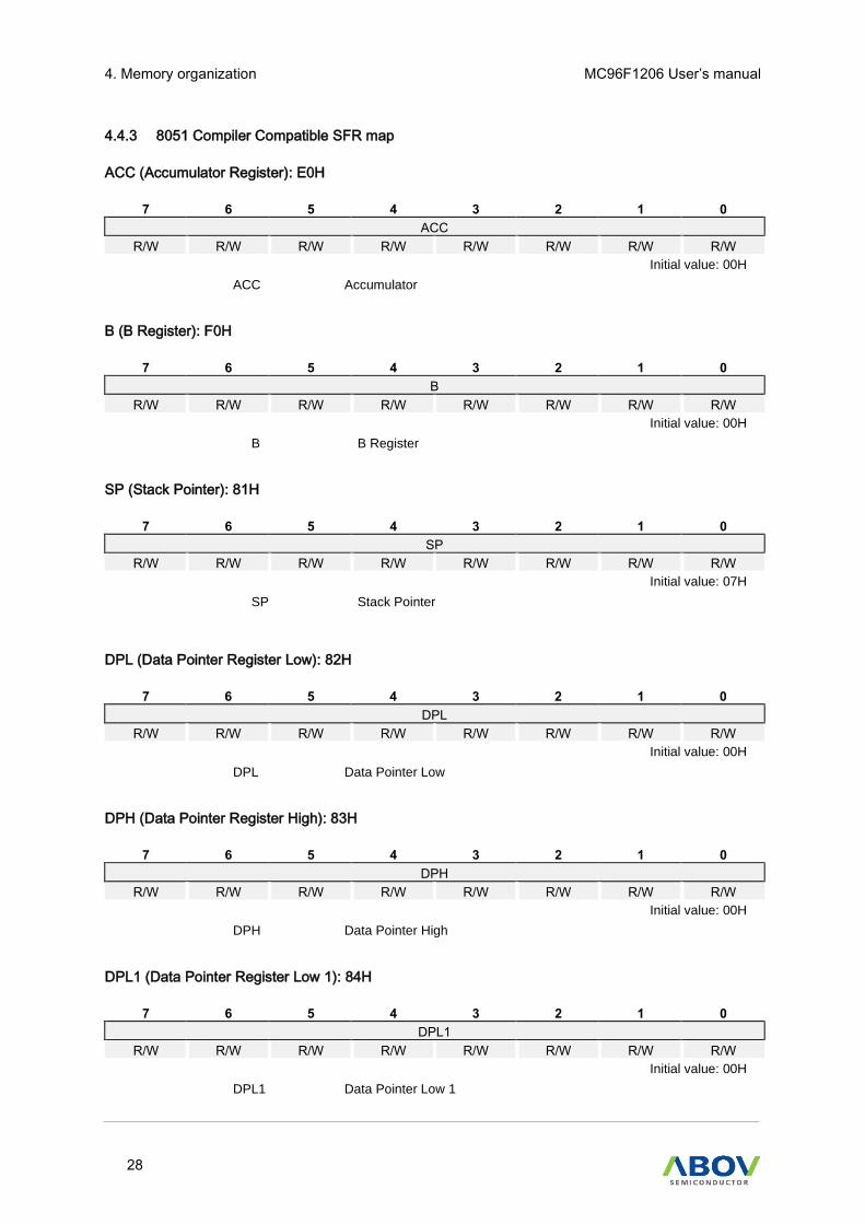
4.4.3 8051 Compiler Compatible SFR map
ACC (Accumulator Register): E0H
7 6 5 4 3 2 1 0
ACC
R/W R/W R/W R/W R/W R/W R/W R/W
Initial value: 00H
ACC Accumulator
B (B Register): F0H
7 6 5 4 3 2 1 0
B
R/W R/W R/W R/W R/W R/W R/W R/W
Initial value: 00H
B B Register
SP (Stack Pointer): 81H
7 6 5 4 3 2 1 0
SP
R/W R/W R/W R/W R/W R/W R/W R/W
Initial value: 07H
SP Stack Pointer
DPL (Data Pointer Register Low): 82H
7 6 5 4 3 2 1 0
DPL
R/W R/W R/W R/W R/W R/W R/W R/W
Initial value: 00H
DPL Data Pointer Low
DPH (Data Pointer Register High): 83H
7 6 5 4 3 2 1 0
DPH
R/W R/W R/W R/W R/W R/W R/W R/W
Initial value: 00H
DPH Data Pointer High
DPL1 (Data Pointer Register Low 1): 84H
7 6 5 4 3 2 1 0
DPL1
R/W R/W R/W R/W R/W R/W R/W R/W
Initial value: 00H
DPL1 Data Pointer Low 1

MC96F1206 User’s manual 4. Memory organization
29
DPH1 (Data Pointer Register High 1): 85H
7 6 5 4 3 2 1 0
DPH1
R/W R/W R/W R/W R/W R/W R/W R/W
Initial value: 00H
DPH1 Data Pointer High 1
PSW (Program Status Word Register): D0H
7 6 5 4 3 2 1 0
CY AC F0 RS1 RS0 OV F1 P
R/W R/W R/W R/W R/W R/W R/W R/W
Initial value: 00H
CY Carry Flag
AC Auxiliary Carry Flag
F0 General Purpose User-Definable Flag
RS1 Register Bank Select bit 1
RS0 Register Bank Select bit 0
OV Overflow Flag
F1 User-Definable Flag
P Parity Flag. Set/Cleared by hardware each instruction cycle to indicate an
odd/even number of ‘1’ bits in the accumulator
EO (Extended Operation Register): A2H
7 6 5 4 3 2 1 0
– – – TRAP_EN – DPSEL2 DPSEL1 DPSEL0
– – – R/W – R/W R/W R/W
Initial value: 00H
TRAP_EN Select the Instruction (Keep always ‘0’).
0 Select MOVC @(DPTR++), A
1 Select Software TRAP Instruction
DPSEL[2:0] Select Banked Data Pointer Register
DPSEL2 DPSEL1 SPSEL0 Description
0 0 0 DPTR0
0 0 1 DPTR1
Reserved

5. Ports MC96F1206 User’s manual
30
Ports
I/O ports
MC96F1206 has two groups of I/O ports, P0 and P1. Each port can be easily configured as an input
pin, an output, or an internal pull up and open-drain pin by software. The port configuration pursues to
meet various system configurations and design requirements. P0 and P1 have a function generating
interrupts in accordance with a change of state of the pin.
Port registers
5.2.1 Data register (Px)
Data register (Px) is related to a bidirectional I/O port. If a port is configured as an output port, data can
be written to the corresponding bit of the Px. If a port is configured as an input, data can be read from
the corresponding bit of the Px.
5.2.2 Direction register (PxIO)
Each I/O pin can be used as an input or an output independently by setting a PxIO register. If a bit is
cleared in this read/write register, the corresponding pin of Px will be an input. While setting bits in this
register will configure the corresponding pins to output.
Most bits are cleared by a system reset, but some bits are set by the system reset.
5.2.3 Pull-up register selection register (PxPU)
On-chip pull-up resistors can be connected to I/O ports individually by configuring a pull-up resistor
selection register (PxPU). Setting a PxPU register can enable or disable a pull-up resister of each port.
If a certain bit in PxPU register is 1, a pull-up resister of the corresponding pin is enabled. While the bit
is 0, the pull-up resister is disabled. All bits are cleared by a system reset.
5.2.4 Open-drain selection register (PxOD)
There are internal open-drain selection registers (PxOD) for P0. Setting a PxOD register can enable or
disable an open-drain of each port.
Most ports become push-pull by a system reset, but some ports become open-drain by the system
reset.
5.2.5 Port function selection register (PSR0,PSR2,PSR3)
Port function selection registers define alternative functions of ports. Please remember that these
registers must be set properly for alternative port functions. A reset clears the PSR0, PSR2, and PSR3
register to ‘00H’, which makes all pins to normal I/O ports.

MC96F1206 User’s manual 5. Ports
31
5.2.6 Pin Change Interrupt Enable Register (PCI)
The P1 can support Pin Change Interrupt function. Pin Change Interrupts PCI will trigger if any enabled
P1[7:0] pin toggles. The PCI Register control which pins contribute to the pin change interrupts.
5.2.7 Register map
Table 5. Port Register Map
Name Address Direction Default Description
P0 80H R/W 00H P0 Data Register
P0IO 89H R/W 00H P0 Direction Register
P0PU D1H R/W 00H P0 Pull-up Resistor Selection Register
P0OD B1H R/W 00H P0 Open-drain Selection Register
P1 88H R/W 00H P1 Data Register
P1IO 91H R/W 00H P1 Direction Register
P1PU D9H R/W 00H P1 Pull-up Resistor Selection Register
P1OD B9H R/W 00H P1 O1pen-drain Selection Register
P2 90H R/W 00H P2 Data Register
P2IO 99H R/W 00H P2 Direction Register
P2PU E1H R/W 00H P2 Pull-up Resistor Selection Register
P2OD C1H R/W 00H P2 Open-drain Selection Register
PCI1 9FH R/W 00H Pin change interrupt enable register
PSR0 DAH R/W 00H Port Debounce selection register
PSR2 DCH R/W 00H P0 Function Selection Register
Port P0
5.3.1 Port description of P0
As an 8-bit I/O port, P0 controls the following registers:
P0 data register (P0)
P0 direction register (P0IO)
P0 pull-up resistor selection register (P0PU)
P0 open-drain selection register (P0OD)
For detailed information of P0 function selection, please refer to Port function selection registers.

5. Ports MC96F1206 User’s manual
32
5.3.2 Register description of P0
P0 (P0 Data Register): 80H
7 6 5 4 3 2 1 0
P07 P06 P05 P04 P03 P02 P01 P00
R/W R/W R/W R/W R/W R/W R/W R/W
Initial value: 00H
P0[7:0] I/O Data
P0IO (P0 Direction Register): 89H
7 6 5 4 3 2 1 0
P07IO P06IO P05IO P04IO P03IO P02IO P01IO P00IO
R/W R/W R/W R/W R/W R/W R/W R/W
Initial value: 00H
P0IO[7:0] P0 Data I/O Direction.
0 Input
1 Output
P0PU (P0 Pull-up Resistor Selection Register): D1H
7 6 5 4 3 2 1 0
P07PU P06PU P05PU P04PU P03PU P02PU P01PU P00PU
R/W R/W R/W R/W R/W R/W R/W R/W
Initial value: 00H
P0PU[7:0] Configure Pull-up Resistor of P0 Port
0 Disable
1 Enable
P0OD (P0 Open-drain Selection Register): B1H
7 6 5 4 3 2 1 0
P07OD P06OD P05OD P04OD P03OD P02OD P01OD P00OD
R/W R/W R/W R/W R/W R/W R/W R/W
Initial value: 00H
P0OD[7:0] Configure Open-drain of P0 Port
0 Push-pull output
1 Open-drain output

MC96F1206 User’s manual 5. Ports
33
Port P1
5.4.1 Port description of P1
As a 6-bit I/O port, P1 controls the following registers:
P1 data register (P1)
P1 direction register (P1IO)
P1 pull-up resistor selection register (P1PU)
P1 open-drain selection register (P1OD)
For detailed information of P1 function selection, please refer to Port function selection registers.
5.4.2 Register description of P1
P1 (P1 Data Register): 88H
7 6 5 4 3 2 1 0
– – P15 P14 P13 P12 P11 P10
– – R/W R/W R/W R/W R/W R/W
Initial value: 00H
P1[5:0] I/O Data
P1IO (P1 Direction Register): 91H
7 6 5 4 3 2 1 0
– – P15IO P14IO P13IO P12IO P11IO P10IO
– – R/W R/W R/W R/W R/W R/W
Initial value: 00H
P1IO[5:0] P1 Data I/O Direction.
0 Input
1 Output
P1PU (P1 Pull-up Resistor Selection Register): D9H
7 6 5 4 3 2 1 0
– – P15PU P14PU P13PU P12PU P11PU P10PU
– – R/W R/W R/W R/W R/W R/W
Initial value: 00H
P1PU[5:0] Configure Pull-up Resistor of P1 Port
0 Disable
1 Enable
P1OD (P1 Open-drain Selection Register): B9H
7 6 5 4 3 2 1 0
– – P15OD P14OD P13OD P12OD P11OD P10OD
– – R/W R/W R/W R/W R/W R/W
Initial value: 00H
P1OD[5:0] Configure Open-drain of P1 Port
0 Push-pull output
1 Open-drain output

5. Ports MC96F1206 User’s manual
34
Port P2
5.5.1 Port description of P2
As a 6-bit I/O port, P2 controls the following registers:
P2 data register (P2)
P2 direction register (P2IO)
P2 pull-up resistor selection register (P2PU)
P2 open-drain selection register (P2OD)
5.5.2 Register description of P2
P2 (P2 Data Register): 90H
7 6 5 4 3 2 1 0
– – – – – – P21 P20
– – – – – – R/W R/W
Initial value: 00H
P2[5:0] I/O Data
P2IO (P2 Direction Register): 99H
7 6 5 4 3 2 1 0
– – – – – – P21IO P20IO
– – – – – – R/W R/W
Initial value: 00H
P2IO[5:0] P2 Data I/O Direction.
0 Input
1 Output
P2PU (P2 Pull-up Resistor Selection Register): E1H
7 6 5 4 3 2 1 0
– – – – – – P21PU P20PU
– – – – – – R/W R/W
Initial value: 00H
P2PU[5:0] Configure Pull-up Resistor of P2 Port
0 Disable
1 Enable
P2OD (P2 Open-drain Selection Register): C1H
7 6 5 4 3 2 1 0
– – – – – – P21OD P20OD
– – – – – – R/W R/W
Initial value: 00H
P2OD[5:0] Configure Open-drain of P2 Port
0 Push-pull output
1 Open-drain output
PSR0 (Port Debounce selection register) : DAH
7 6 5 4 3 2 1 0
– – – – – – PSR01 PSR00
– – – – – – R/W R/W
MC96F1206 User’s manual 5. Ports
35
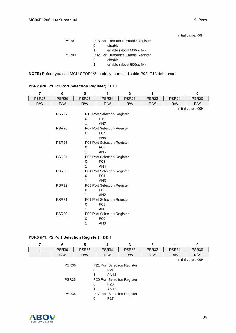
Initial value: 00H
PSR01 P13 Port Debounce Enable Register
0 disable
1 enable (about 500us fix)
PSR00 P02 Port Debounce Enable Register
0 disable
1 enable (about 500us fix)
NOTE) Before you use MCU STOP1/2 mode, you must disable P02, P13 debounce.
PSR2 (P0, P1, P2 Port Selection Register) : DCH
7 6 5 4 3 2 1 0
PSR27 PSR26 PSR25 PSR24 PSR23 PSR22 PSR21 PSR20
R/W R/W R/W R/W R/W R/W R/W R/W
Initial value: 00H
PSR27 P10 Port Selection Register
0 P10
1 AN7
PSR26 P07 Port Selection Register
0 P07
1 AN6
PSR25 P06 Port Selection Register
0 P06
1 AN5
PSR24 P05 Port Selection Register
0 P05
1 AN4
PSR23 P04 Port Selection Register
0 P04
1 AN3
PSR22 P03 Port Selection Register
0 P03
1 AN2
PSR21 P01 Port Selection Register
0 P01
1 AN1
PSR20 P00 Port Selection Register
0 P00
1 AN0
PSR3 (P1, P2 Port Selection Register) : DDH
7 6 5 4 3 2 1 0
- PSR36 PSR35 PSR34 PSR33 PSR32 PSR31 PSR30
- R/W R/W R/W R/W R/W R/W R/W
Initial value: 00H
PSR36
P21 Port Selection Register
0 P21
1 AN14
PSR35
P20 Port Selection Register
0 P20
1 AN13
PSR34
P17 Port Selection Register
0 P17

5. Ports MC96F1206 User’s manual
36
1 AN12
PSR33
P16 Port Selection Register
0 P16
1 AN11
PSR32
P15 Port Selection Register
0 P15
1 AN10
PSR31
P14 Port Selection Register
0 P14
1 AN9
PSR30
P13 Port Selection Register
0 P13
1 AN8
PSRPWM (PWM Port Selection Register) : DEH
7 6 5 4 3 2 1 0
- PSRPWM6 PSRPWM5 PSRPWM4 - PSRPWM2 PSRPWM1 PSRPWM0
- R/W R/W R/W - R/W R/W R/W
Initial value: 00H
PSRPWM[6:4] PWM1 Ports Selection Register
0 PWM1 out to P04(default)
1 PWM1 out to P05
2 PWM1 out to P06
3 PWM1 out to P07
4 PWM1 out to P14
5 PWM1 out to P15
6 PWM1 out to P16
7 PWM1 out to P17
PSRPWM[2:0] PWM0 Ports Selection Register
0 PWM0 out to P04(default)
1 PWM0 out to P05
2 PWM0 out to P06
3 PWM0 out to P07
4 PWM0 out to P14
5 PWM0 out to P15
6 PWM0 out to P16
7 PWM0 out to P17
NOTE) When using ports as PWM0 and PWM1 output port (PSRPWM=0x00), PWM0 is preferentially operated.

MC96F1206 User’s manual 6. Interrupt controller
37
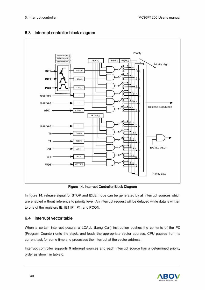
Interrupt controller
Up to 16 interrupt sources are available in the MC96F1206. Allowing software control, each interrupt
source can be enabled by defining separate enable register bit associated with it. It can also have four
levels of priority assigned. The non-maskable interrupt source is always enabled with a higher priority
than any other interrupt sources, and is not controllable by software.
The interrupt controller features the followings:
Receives requests from 9 interrupt sources
6 group priority
4 priority levels
Multi interrupt possibility
If requests of different priority levels are received simultaneously, a request with higher priority
level is served first.
Each interrupt source can be controlled by an EA bit and an IEx bit
Interrupt latency varies ranging from 5 to 8 machine cycles in a single interrupt system.
Non-maskable interrupt is always enabled, while maskable interrupts can be enabled through four pairs
of interrupt enable registers (IE, IE1). Each bit of the four registers can individually enable or disable a
particular interrupt source. Especially bit 7 (EA) in the register IE provides overall control. It must be set
to ‘1’ to enable interrupts as introduced in the followings:
When EA is set to ‘0’ all interrupts are disabled.
When EA is set to ‘1’ a particular interrupt can be individually enabled or disabled by the
associate bit of the interrupt enable registers.
EA is always cleared to ‘0’ jumping to an interrupt service vector and set to ‘1’ executing the [RETI]
instruction. MC96F1206 supports a four-level priority scheme. Each maskable interrupt is individually
assigned to one of the four levels according to IP and IP1.

6. Interrupt controller MC96F1206 User’s manual
38
Figure 11. Interrupt Group Priority Level
Figure 13 introduces interrupt groups and their priority levels that is available for sharing interrupt priority.
Priority of a group is set by 2 bits of Interrupt Priority (IP) registers: 1 bit from IP and another 1 bit from
IP1.
Interrupt Service Routine serves an interrupt having higher priority first. If two requests of different
priority levels are received simultaneously, the request with higher priority level is served prior to the
lower one.
External interrupt
External interrupts on pins of INT0, INT1 receive various interrupt requests in accordance with the
external interrupt polarity 0 register (EIPOL0) and external interrupt polarity 1 register (EIPOL1) as
shown in figure 14. Each external interrupt source has enable/disable bits. An external interrupt flag
register (EIFLAG) provides status of the external interrupts.
Pin Change Interrupt
The pin change interrupt on P1 ports receive the both edge (Falling-edge and Rising-edge) interrupt
request as shown in Figure13. Also each pin change interrupt source has enable setting bits. The FLAG
(flag register) register provides the status of ports change interrupts.

MC96F1206 User’s manual 6. Interrupt controller
39
Figure 12. External Interrupt Description
Figure 13. PCI Interrupt Description
6. Interrupt controller MC96F1206 User’s manual
40
Interrupt controller block diagram
Release Stop/Sleep
EA(IE.7[A8H])
Priority High
IE[A8H]
-
INT0
INT1
ADC EXTRG
0
1
2
3
4
5
0
1
2
3
4
5
0
1
2
3
4
5
0
1
2
3
4
5
IP[B8H] IP1[F8H]EIPOLA[A6H]
EIBOTH[A7H]
TMIF1
LVIRF
IE1[A9H]
BITF
WDTIFR
LVI
8
9
10
11
8
9
10
11
8
9
10
11
8
9
10BIT
WDT11
-
TMIF0
77
77
66
66-
T0
T1
PCI1
reserved
EIEDGE[A5H]
FLAG2
FLAG0
FLAG1
reserved
reserved
Priority Low
Priority
Figure 14. Interrupt Controller Block Diagram
In figure 14, release signal for STOP and IDLE mode can be generated by all interrupt sources which
are enabled without reference to priority level. An interrupt request will be delayed while data is written
to one of the registers IE, IE1 IP, IP1, and PCON.
Interrupt vector table
When a certain interrupt occurs, a LCALL (Long Call) instruction pushes the contents of the PC
(Program Counter) onto the stack, and loads the appropriate vector address. CPU pauses from its
current task for some time and processes the interrupt at the vector address.
Interrupt controller supports 9 interrupt sources and each interrupt source has a determined priority
order as shown in table 6.

MC96F1206 User’s manual 6. Interrupt controller
41
Table 6. Interrupt Vector Address Table
Interrupt source Symbol Interrupt
Enable Bit
Priority Mask Vector
address
Hardware Reset RESETB 0 0 Non-Maskable 0000H
External Interrupt 0 INT0 IE.0 1 Maskable 0003H
External Interrupt 1 INT1 IE.1 2 Maskable 000BH
PCI INT2 IE.2 3 Maskable 0013H
- INT3 IE.3 4 Maskable 001BH
- INT4 IE.4 5 Maskable 0023H
ADC INT5 IE.5 6 Maskable 002BH
- INT6 IE.6 7 Maskable 0033H
TIMER 0 INT7 IE1.1 8 Maskable 003BH
TIMER 1 INT8 IE1.2 9 Maskable 0043H
LVI INT9 IE1.3 10 Maskable 004BH
BIT INT10 IE1.4 11 Maskable 0053H
WDT INT11 IE1.5 12 Maskable 005BH
To execute the maskable interrupts, both EA bit and a corresponding bit of IEx associated with a specific
interrupt source must be set to ‘1’. When an interrupt request is received, a particular interrupt request
flag is set to ‘1’ and maintains its status until CPU accepts the interrupt. After the interrupt acceptance,
the interrupt request flag will be cleared automatically.
Interrupt sequence
An interrupt request is held until the interrupt is accepted or the interrupt latch is cleared to ‘0’ by a
reset or an instruction. The interrupt acceptance always happens at the last cycle of the instruction
process. So rather than fetching the current instruction, CPU executes internally LCALL instruction and
saves a PC onto the stack.
To begin an ISR (Interrupt Service Routine), the interrupt controller uses a branch instruction LJMP
(Long Jump). The interrupt controller gives address of LJMP instruction to CPU. Since the end of the
execution of current instruction, it needs 5~8 machine cycles to go to the interrupt service routine. The
interrupt service task is terminated by the interrupt return instruction [RETI]. Once an interrupt request
is generated, the following process is performed.
Table 7 introduces LJMP example code.

6. Interrupt controller MC96F1206 User’s manual
42
Table 7. LJMP Description and Example Code
Instruction LJMP
Example code LJMP 4000H
NOTE: After finishing LJMP, NOP located at the address 400H will be executed as the next instruction.
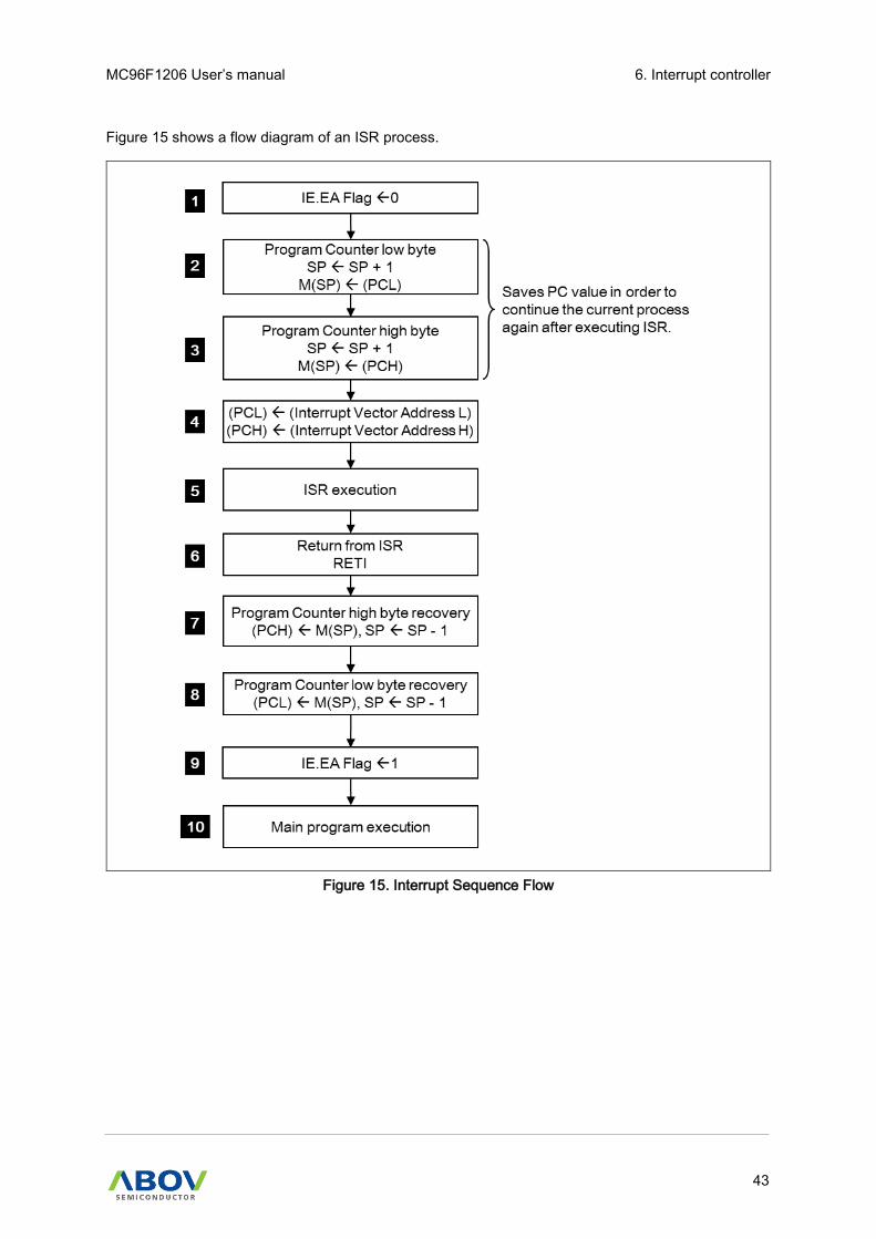
MC96F1206 User’s manual 6. Interrupt controller
43
Figure 15 shows a flow diagram of an ISR process.
Figure 15. Interrupt Sequence Flow

6. Interrupt controller MC96F1206 User’s manual
44
Effective timing after controlling interrupt bit
Case A in figure 16 shows an effective time of Control Interrupt Enable Register (IE, IE1).
Figure 16. Case A: Effective Timing of Interrupt Enable Register
Case B in figure 17 shows an effective time of Interrupt Flag Register.
Figure 17. Case B: Effective Timing of Interrupt Flag Register
Multi interrupt
If two requests of different priority levels are received simultaneously, the request with higher priority
level is served first. If more than one interrupt request are received, the interrupt polling sequence
determines which request is served first by hardware. However, for special features, multi-interrupt
processing can be executed by software.

MC96F1206 User’s manual 6. Interrupt controller
45
Figure 18. Effective Timing of Multi Interrupt
Figure 17 shows an example of multi-interrupt processing. While INT1 is served, INT0 which has higher
priority than INT1 is occurred. Then INT0 is served immediately, then remain part of INT1 service routine
is executed. If the priority level of INT0 is same or lower than INT1, INT0 will be served after the INT1
service has completed.
An interrupt service routine can be interrupted only by an interrupt with higher priority, and if two
interrupts of different priority occur at the same time, the interrupt with higher priority level will be served
first. An interrupt cannot be interrupted by another interrupt with the same or a lower priority level. If two
interrupts having the same priority level occur simultaneously, the service order for those interrupts will
be determined by the scan order.
Interrupt enable accept timing
Figure 19 implies that some period of time is required to response to the latched interrupt signal. In
figure 19, 5machine cycles will be taken for the processes of LCALL and LJMP.

6. Interrupt controller MC96F1206 User’s manual
46
Figure 19. Interrupt Response Timing Diagram
Interrupt Service Routine Address
As seen in figure 20, ISR can be placed at any other location in program memory, and program memory
must provide an unconditional jump to the starting address of ISR from the corresponding vector
address.
Figure 20. Correspondence between Vector Table Address and ISR Entry Address
Saving/ restore general-purpose registers
Let’s assume there occurs an urgent condition. CPU needs to pause from its current task (Main Task
in figure 21) for some time to execute something else (Interrupt Service Task in figure 21). After finishing
the something else, CPU will return to the current task (Main Task).

MC96F1206 User’s manual 6. Interrupt controller
47
Figure 21. Saving and Restore Process Diagram and Example Code
Example code in figure 21 performs the followings:
1. Interrupt INTXX occurs.
2. PUSH PSW: the SP is incremented by one, and the value of the specified byte operand is
stored at the internal RAM address indirectly referenced by the SP.
3. PUSH DPL, PUSH DPH: PSW in memory stack by help of PUSH instruction.
4. CPU stores low
5. CPU pops the value of flag register and stores it in register H by help of POP Instruction.
Interrupt timing
As seen in figure 22 below, an interrupt source is sampled at the last cycle of a command. Upon the
sampling, low 8-bit of interrupt vector is decided. M8051W core makes the interrupt acknowledge at the
first cycle of a command, executes LCALL instruction to jump interrupt routine at the address referenced
by INT_VEC.

6. Interrupt controller MC96F1206 User’s manual
48
NOTES: Command cycle CLPx imply the followings:
1. L Last cycle
2. 1 1st cycle or 1st phase
3. 2 2nd cycle or 2nd phase
Figure 22. Timing Chart of Interrupt Acceptance and Interrupt Return Instruction
Interrupt register
Interrupt registers are memory space used to control interrupt functions. As shown in table 10, the
interrupt registers consist of Interrupt Enable Registers, Interrupt Priority Registers, External Interrupt
Flag Registers, and External Interrupt Polarity Register.
6.12.1 Interrupt Enable registers (IE, IE1)
Interrupt enable register consists of global interrupt control bit (EA) and peripheral interrupt control bits.
Total 12 peripherals are able to control interrupts.
6.12.2 Interrupt Priority registers (IP, IP1)
12 interrupts are divided into 3 groups where each group has 4 interrupt sources respectively. A group
can be assigned 4 levels of interrupt priority by using an interrupt priority register. Level 3 is the highest
priority, while level 0 is the lowest priority. After a reset, IP and IP1 are cleared to ‘00H’. If interrupts
have the same priority level, lower number interrupt is served first.
6.12.3 External Interrupt Flag register (EIFLAG)
External interrupt flag (EIFLAG) is set to ‘1’ when the external interrupt generating condition is satisfied.

MC96F1206 User’s manual 6. Interrupt controller
49
The flag is cleared when the interrupt service routine is executed. Alternatively, the flag can be cleared
by writing ‘0’ to it.
6.12.4 External Interrupt Polarity registers (EIPOL0, EIPOL1)
External interrupt polarity 0 register (EIPOL0) and external interrupt polarity 1 register (EIPOL1)
determine one from rising edge, falling edge, and both edges for interrupt. No interrupt is at any edge
by default.
6.12.5 Register map
Table 8. Interrupt Register Map
Name Address Direction Default Description
IE A8H R/W 00H Interrupt Enable Register
IE1 A9H R/W 00H Interrupt Enable Register 1
IP B8H R/W 00H Interrupt Priority Register
IP1 F8H R/W 00H Interrupt Priority Register 1
EIENAB A3H R/W 00H Interrupt Enable Register
EIFLAG A4H R/W 00H Interrupt Flag Register
EIEDGE A5H R/W 00H Interrupt Edge Register
EIPOLA A6H R/W 00H Interrupt Polarity Register
EIBOTH A7H R/W 00H Interrupt Both Edge Register
6.12.6 Interrupt register description
Interrupt registers are used to control interrupt functions. In addition to external interrupt control registers,
these interrupt registers consist of interrupt enable register (IE) and interrupt enable register 1 (IE1).
For external interrupt, there are external interrupt flag register (EIFLAG), external interrupt polarity 0/1
registers (EIPOL0/1), and external interrupt flag register (EIFLAG).

6. Interrupt controller MC96F1206 User’s manual
50
IE (Interrupt Enable Register): A8H
7 6 5 4 3 2 1 0
EA - INT5E - - INT2E INT1E INT0E
R/W - R/W - - R/W R/W R/W
Initial value: 00H
EA
Enable or disable all interrupt bits
0 All Interrupt disable
1 All Interrupt enable
INT5E
Enable or disable ADC Interrupt
0 ADC interrupt Disable
1 ADC interrupt Enable
INT2E
Enable or disable Pin Change Interrupt
0 Pin Change Interrupt Disable
1 Pin Change Interrupt Enable
INT1E
Enable or disable External Interrupt 1
0 External interrupt 1 Disable
1 External interrupt 1 Enable
INT0E
Enable or disable External Interrupt 0
0 External interrupt 0 Disable
1 External interrupt 0 Enable
IE1 (Interrupt Enable Register 1): A9H
7 6 5 4 3 2 1 0
- - INT11E INT10E INT9E INT8E INT7E -
- - R/W R/W R/W R/W R/W -
Initial value: 00H
INT11E Enable or disable WDT Interrupt
0 WDT interrupt Disable
1 WDT interrupt Enable
INT10E Enable or disable BIT Interrupt
0 BIT interrupt Disable
1 BIT interrupt Enable
INT9E Enable or disable LVI Interrupt
0 LVI interrupt Disable
1 LVI interrupt Enable
INT8E Enable or disable Timer 1 Interrupt
0 Timer1 interrupt Disable
1 Timer1 interrupt Enable
INT7E Enable or disable Timer 0 Interrupt
0 Timer0 interrupt Disable
1 Timer0 interrupt Enable

MC96F1206 User’s manual 6. Interrupt controller
51
IP (Interrupt Priority Register): B8H
7 6 5 4 3 2 1 0
– – IP5 IP4 IP3 IP2 IP1 IP0
– – R/W R/W R/W R/W R/W R/W
Initial value: 00H
IP1 (Interrupt Priority Register 1): F8H
7 6 5 4 3 2 1 0
– – IP15 IP14 IP13 IP12 IP11 IP10
– – R/W R/W R/W R/W R/W R/W
Initial value: 00H
IP[5:0], IP1[5:0] Select Interrupt Group Priority
IP1x IPx Description
0 0 level 0 (lowest)
0 1 level 1
1 0 level 2
1 1 level 3 (highest)
EIENAB (External Interrupt Enable Register) : A3H
7 6 5 4 3 2 1 0
- - - - - - ENAB1 ENAB0
- - - - - - R/W R/W Initial value: 0H
ENAB1 Enable or Disable External Interrupt 1
0 Disable External Interrupt 1(default)
1 Enable External Interrupt 1
ENAB0 Enable or Disable External Interrupt 0
0 Disable External Interrupt 0(default)
1 Enable External Interrupt 0
EIFLAG (External Interrupt Flag Register): A4H
7 6 5 4 3 2 1 0
–- – – – – FLAG2 FLAG1 FLAG0
– – – – – R/W R/W R/W
Initial value: 00H
If External Interrupt is occurred, the flag becomes ‘1’. The flag can
be cleared by writing a ‘0’ to bit. It is also cleared automatically
after interrupt service routine is served.
FLAG2 When Pin Change Interrupt is occurred this bit is set.
0 Pin Change Interrupt is not occurred
1 Pin Change Interrupt is occurred
FLAG1 When External Interrupt 1 is occurred this bit is set.
0 External Interrupt 1 is not occurred
1 External Interrupt 1 is occurred
FLAG0 When External Interrupt 0 is occurred this bit is set.
0 External Interrupt 0 is not occurred
1 External Interrupt 0 is occurred
EIEDGE (External Interrupt Edge Register) : A5H

6. Interrupt controller MC96F1206 User’s manual
52
7 6 5 4 3 2 1 0
–- – – – – – FLAG1 FLAG0
– – – – – – R/W R/W Initial value : 0H
EDGE1 Determines the type of External interrupt 1, edge or level sensitive.
0 Level (default)
1 Edge
EDGE0 Determines the type of External interrupt 0, edge or level sensitive.
0 Level (default)
1 Edge
EIPOLA (External Interrupt Polarity Register) : A6H
Initial value: 00H
7 6 5 4 3 2 1 0
- - - - - - POLA1 POLA0
- - - - - - R/W R/W Initial value: 0H
According to EIEDGE, this register acts differently. If EIEDGE is
level type, external interrupt polarity have level value. If EIEDGE is
edge type, external interrupt polarity have edge value.
POLA1 Determine the polarity of External Interrupt 1
0 When High level or rising edge, Interrupt occur(default)
1 When Low level or falling edge, Interrupt occur
POLA0 Determine the polarity of External Interrupt 0
0 When High level or rising edge, Interrupt occur(default)
1 When Low level or falling edge, Interrupt occur
EIBOTH (External Interrupt Both Edge Enable Register) : A7H
7 6 5 4 3 2 1 0
- - - - - - BOTH1 BOTH0
- - - - - - R/W R/W Initial value: 0H
If BOTHx is written to ‘1’, the corresponding external pin interrupt is
enabled by both edges (no level).
And EIEDGE and EIPOLA register value are ignored.
BOTH1
Determine the type of External Interrupt 1
0 Both edge detection Disable (default)
1 Both edge detection Enable
BOTH0
Determine the type of External Interrupt 0
0 Both edge detection Disable (default)
1 Both edge detection Enable

MC96F1206 User’s manual 7. Clock generator
53
Clock generator
The clock generator produces the basic clock pulses which provide the system clock to CPU and
peripheral hardware. The internal RC-OSC is used as system clock and the default division rate is two.
- Calibrated Internal RC Oscillator (32MHz)
. INTERNAL CLOCK(16MHz)/1 (16MHz)
. INTERNAL CLOCK(16MHz)/2 (8MHz, Default system clock)
. INTERNAL CLOCK(16MHz)/4 (4MHz)
. INTERNAL CLOCK(16MHz)/16 (1MHz)
Block diagram
Figure 23. Clock Generator in Block Diagram
Register map
Table 9. Clock Generator Register Map
Name Address Direction Default Description
SCCR 8AH R/W 20H System and Clock Control Register
Register description
Clock generator registers use the clock control for system operation. The clock generator consists of
System and clock control register, oscillator control register internal RC trim control register, internal
RC trim register, and internal RC identification register.

7. Clock generator MC96F1206 User’s manual
54
SCCR (System and Clock Control Register): 8AH
7 6 5 4 3 2 1 0
STOP1 DIV1 DIV0 CBYS ISTOP - - CS
R/W R/W R/W R/W R/W - - R/W
Initial value: 20H
STOP1 Control the STOP Mode
NOTE)
When PCON=0x03, This bit is applied. When PCON=0x01, This bit
is not applied.
0 STOP2 Mode (at PCON=0x03) (default)
1 STOP1 Mode (at PCON=0x03)
DIV[1:0] When using internal clock as system clock, determine division rate.
NOTE) when using internal clock as system clock, only division
rate come into effect.
NOTE) To change by software, CBYS set to ‘1’
DIV1 DIV0 description
0 0 1-Div (16MHz)
0 1 2-Div (8MHz, default system clock)
1 0 4-Div (4MHz)
1 1 16-Div (1MHz)
CBYS Control the scheme of clock change. If this bit set to ‘0’, clock
change is controlled by hardware. But if this set to ‘1’, clock
change is controlled by software. Ex) when setting CS, if CBYS bit
set to ‘0’, it is not changed right now, CPU goes to STOP mode
and then when wake-up, it applies to clock change.
NOTE) when clear this bit, keep other bits in SCCR.
0 Clock changed by hardware during stop mode (default)
1 Clock changed by software
ISTOP Control the operation of INT-RC Oscillation
NOTE) when CBYS=’1’, It is applied
0 RC-Oscillation enable (default)
1 RC-Oscillation disable
CS Determine System Clock
NOTE) by CBYS bit, reflection point is decided
CS Description
0 System clock (default 8MHz)
1 fWDTOSC (8 kHz)

MC96F1206 User’s manual 8. Basic interval timer
55
Basic interval timer
The MC96F1206 has one 8-bit Basic Interval Timer that is free-run and can’t stop. Block diagram is
shown in . In addition, the Basic Interval Timer generates the time base for watchdog timer counting. It
also provides a Basic interval timer interrupt (BITF).
During Power On, BIT gives a stable clock generation time
On exiting Stop mode, BIT gives a stable clock generation time
As clock function, time interrupt occurrence
Block diagram
Figure 24. Basic Interval Timer in Block Diagram
Register map
Table 10. Basic Interval Timer Register Map
Name Address Direction Default Description
BCCR 8BH R/W 06H BIT Clock Control Register
BITR 8CH R 00H Basic Interval Timer Register
Register description
The Bit Interval Timer Register consists of BIT Clock control register (BCCR) and Basic Interval Timer
register (BITR). If BCLR bit set to ‘1’, BITR becomes ‘0’ and then counts up. After 1 machine cycle,
BCLR bit is cleared as ‘0’ automatically.

8. Basic interval timer MC96F1206 User’s manual
56
BCCR (BIT Clock Control Register) : 8BH
7 6 5 4 3 2 1 0
BITF - - IRC_SEL BCLR BCK2 BCK1 BCK0
R/W R R RW R/W R/W R/W R/W Initial value : 06H
BITF When BIT Interrupt occurs, this bit becomes ‘1’. For clearing bit, write ‘0’
to this bit.
0 no generation
1 generation
IRC_SEL BIT Clock source select
0 WDT 8kHz
1 64kHz (IRC Clock source)
BCLR If BCLR Bit is written to ‘1’, BIT Counter is cleared as ‘0’
0 Free Running
1 Clear Counter
BCK[2:0] Select BIT overflow period (ex) BIT Clock ≒ 8kHz)
BCK2 BCK1 BCK0
0 0 0 0.25msec ( BIT Clock * 2)
0 0 1 0.50msec
0 1 0 1.00msec
0 1 1 2.00msec
1 0 0 4.00msec
1 0 1 8.00msec
1 1 0 16.0msec (default)
1 1 1 32.0msec
Table 11. BIT period Table
BCK[2:0] WDT 8kHz
(IRCSEL=0)
IRC divider 64kHz
(IRCSEL=1)
000 0.25 msec 0.03125 msec
001 0.50 msec 0.0625 msec
010 1.00 msec 0.125 msec
011 2.00 msec 0.250 msec
100 4.00 msec 0.500 msec
101 8.00 msec 1.000 msec
110 (default) 16.00 msec 2.000 msec
111 32.00 msec 4.000 msec
BITR (Basic Interval Timer Register) : 8CH
7 6 5 4 3 2 1 0
BIT7 BIT6 BIT5 BIT4 BIT3 BIT2 BIT1 BIT0
R R R R R R R R
Initial value : 00H
BIT[7:0] BIT Counter

MC96F1206 User’s manual 9. Watchdog timer
57
Watchdog timer
The watchdog timer rapidly detects the CPU malfunction such as endless looping caused by noise or
the like, and resumes the CPU to the normal state. The watchdog timer signal for detecting malfunction
can be selected either a reset CPU or an interrupt request. When the watchdog timer is not being used
for malfunction detection, it can be used as a timer to generate an interrupt at fixed intervals. It is
possible to use free running 8-bit timer mode (WDTRSON=’0’) or watch dog timer mode
(WDTRSON=’1’) as setting WDTMR[6] bit. If writing WDTMR[5] to ‘1’, WDT counter value is cleared
and counts up. After 1 machine cycle, this bit has ‘0’ automatically. The watchdog timer consists of 8-
bit binary counter and the watchdog timer data register. When the value of 8-bit binary counter is equal
to the 8 bits of WDTR, the interrupt request flag is generated. This can be used as Watchdog timer
interrupt or reset the CPU in accordance with the bit WDTRSON.
The clock source of Watch Dog Timer is BIT overflow output. The interval of watchdog timer interrupt
is decided by BIT overflow period and WDTR set value. The equation is as below
Block diagram
BIT OverflowWDTCR
Watchdog Timer
Counter Register
WDTR
[8EH]
[8EH]
comparator
WDTMR
Watchdog Timer Register
Clear
WDTCL WDTRSON
WDTIFR
Clear
WDTEN
INT_ACK
To Reset
Circuit
To interrupt
block
Figure 25. Watchdog Timer in Block Diagram
WDT interrupt timing waveform
Figure 26 shows a timing diagram when a watchdog timer generates system reset signal and an
interrupt signal.
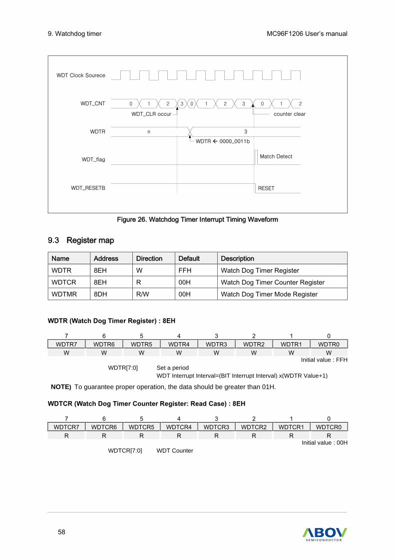
9. Watchdog timer MC96F1206 User’s manual
58
0
WDT Clock Sourece
WDT_flag
WDT_RESETB
WDT_CNT 1 2 3 0 1 2 3 0 1 2
WDTR 3n
counter clearWDT_CLR occur
WDTR ß 0000_0011b
RESET
Match Detect
Figure 26. Watchdog Timer Interrupt Timing Waveform
Register map
Name Address Direction Default Description
WDTR 8EH W FFH Watch Dog Timer Register
WDTCR 8EH R 00H Watch Dog Timer Counter Register
WDTMR 8DH R/W 00H Watch Dog Timer Mode Register
WDTR (Watch Dog Timer Register) : 8EH
7 6 5 4 3 2 1 0
WDTR7 WDTR6 WDTR5 WDTR4 WDTR3 WDTR2 WDTR1 WDTR0
W W W W W W W W Initial value : FFH
WDTR[7:0] Set a period
WDT Interrupt Interval=(BIT Interrupt Interval) x(WDTR Value+1)
NOTE) To guarantee proper operation, the data should be greater than 01H.
WDTCR (Watch Dog Timer Counter Register: Read Case) : 8EH
7 6 5 4 3 2 1 0
WDTCR7 WDTCR6 WDTCR5 WDTCR4 WDTCR3 WDTCR2 WDTCR1 WDTCR0
R R R R R R R R Initial value : 00H
WDTCR[7:0] WDT Counter

MC96F1206 User’s manual 9. Watchdog timer
59
WDTMR (Watch Dog Timer Mode Register) : 8DH
7 6 5 4 3 2 1 0
WDTEN WDTRSON WDTCL - - - - WDTIFR
R/W R/W R/W - - - - R/W Initial value : 00H
WDTEN Control WDT operation
0 disable
1 enable
WDTRSON Control WDT Reset operation
0 Free Running 8-bit timer
1 Watch Dog Timer Reset ON
WDTCL Clear WDT Counter
0 Free Run
1 Clear WDT Counter (auto clear after 1 Cycle)
WDTIFR When WDT Interrupt occurs, this bit becomes ‘1’. For clearing bit, write
‘0’ to this bit or auto clear by INT_ACK signal.
0 WDT Interrupt no generation
1 WDT Interrupt generation

10. Timer MC96F1206 User’s manual
60
TIMER
The 16-bit timer x(0~1) consists of Multiplexer, Timer Data Register High/Low, Timer Register High/Low,
Timer Mode Control Register, PWM Duty High/Low, PWM Period High/Low Register. It is able to use
internal 16-bit timer/ counter without a port output function. The 16-bit timer x can be clocked by internal
or external clock source (EC0, EC1). The divided clock of the main clock selected from prescaler output.
T32M in the T0CR1 register is select internal-RCOSC(32MHz) as Timer0 clock source.
16-bit timer/ counter mode
In the 16-bit Timer/Counter Mode, If the TxH + TxL value and the TxDRH + TxDRL value are matched,
Tx/PWMx port outputs. The output is 50:50 of duty square wave, the frequency is following.
)1(ValuePrescaler 2
FrequencyClock Timer
+=
TxDRCOMPf
fCOMP is timer output frequency and TxDR is the 16 bits value of TxDRH and TxDRL.To export the
compare output as Tx/PWMx, the Tx_PE bit in the TxCR1 register must set to ‘1’.The 16-bit
Timer/Counter Mode is selected by control registers as shown in Figure 27. When TxH, TxL are read,
TxL should be read first. Because when TxL is read TxH is captured to buffer, and when TxH is read
captured value of TxH is read.
.

MC96F1206 User’s manual 10. Timer
61
Figure 27. 16-bit Timer/ Counter Mode of TIMER 0/1
Figure 28. 16-bit Timer/ Counter 0/1 Interrupt Example
16-bit capture mode
The timer x(0~1) capture mode is set by CAPx as ‘1’ in TxCR register. The clock is same source as
Output Compare mode. The interrupt occurs at TxH, TxL and TxDRH, TxDRL matching time. The
capture result is loaded into CDRxH, CDRxL. The TxH, TxL value is automatically cleared(0000H) by
hardware and restarts counter.
This timer interrupt in capture mode is very useful when the pulse width of captured signal is wider than
the maximum period of timer. As the EIEDGE and EIPOLA and EIBOTH register setting, the external

10. Timer MC96F1206 User’s manual
62
interrupt INTx function is chosen.
The CDRxH, PWMxDRH and TxH are in same address. In the capture mode, reading operation is read
the CDRxH, not TxH because path is opened to the CDRxH. PWMxDRH will be changed in writing
operation. The PWMxDRL, TxL, CDRxL has the same function.
Figure 29. 16-bit Capture Mode of TIMER 0/1

MC96F1206 User’s manual 10. Timer
63
Figure 30. Input Capture Mode Operation of TIMER 0/1
Figure 31. Express Timer Overflow in Capture Mode

10. Timer MC96F1206 User’s manual
64
PWM Mode
The timer x(0~1) has a PWM (pulse Width Modulation) function. In PWM mode, the Tx/PWMx output
pin outputs up to 16-bit resolution PWM output. This pin should be configured as a PWM output by set
TX_PE to ‘1’. The PWM output mode is determined by the PWMxPRH, PWMxPRL, PWMxDRH and
PWMxDRL. And you should configure PWMxE bit to “1” in TxCR register before write to PWM registers.
• PWM Period = (PWMxPRH, PWMxPRL + 1) X Timerx Clock Period
• PWM Duty = (PWMxDRH, PWMxDRL + 1) X Timerx Clock Period
Table 12. PWM Frequency vs. Resolution at 16MHz and 32MHz
Resolution
Frequency (MC96F1206)
T32M = 1
T32M = 0
TxCK[2:0]=000
(62.5ns)
T32M = 0
TxCK[2:0]=001
(250ns)
T32M = 0
TxCK[2:0]=010
(500ns)
16-bit 488.281 Hz 244.141 Hz 61.035 Hz 30.517 Hz
15-bit 976.563 Hz 488.281 Hz 122.07 Hz 61.035 Hz
10-bit 31.250 kHz 15.625 kHz 3.906 kHz 1.953 kHz
9-bit 62.500 kHz 31.250 kHz 7.812 kHz 3.906 kHz
8-bit 125.00 kHz 62.500 kHz 15.625 kHz 7.812 kHz
In PWM mode, the duty value and counter matching enables the period value and counter comparison.
After counter and the period value matching, counter restarts. If the duty value is set same to the period
value, counter doesn't restart after the duty value and counter matching. It is highly recommended that
the duty value is not set same to the period value. PWM Period and Duty same output shown Figure
32. The POL bit of TxCR register decides the polarity of duty cycle
Figure 32. PWMx Mode Block Diagram

MC96F1206 User’s manual 10. Timer
65
Figure 33. Example of PWM at 8MHz
Figure 34. Example of PWM at 8MHz(Duty=Period)
Timer Data and Period/Duty Write
When writing a value to the Timer x data registers, write to the TxDRH first, then write to the TxDRL.
When writing to the high register, it is stored in a temporary buffer. When writing to the low register,
temporary buffer is saved the data high register. Timer period/duty registers (PWMxDRH, PWMxDRL,
PWMxPRH, PWMxPRL) operate in the same way.

10. Timer MC96F1206 User’s manual
66
Whenever the counter is started, data high/low registers are loaded to the compare registers.
TxH/L (16-bit Counter)
TxDRLTxDRH
TxDRH_BUF
TxDRL write
TxDRH write
Compare
Data Low RegisterData High Register
Timer x start
Figure 35. Timer x Compare Data Write
Register map
Table 13. TIMER 0 Register Map
Name Address Direction Default Description
T0CR B2H R/W 00H Timer 0 Mode Control Register
T0CR1 B3H R/W 00H Timer 0 Mode Control Register 1
T0L B4H R 00H Timer 0 Low Register
PWM0DRL B4H R/W 00H PWM 0 Duty Register Low
CDR0L B4H R 00H Timer 0 Capture Data Register Low
T0H B5H R 00H Timer 0 Register High
PWM0DRH B5H R/W 00H PWM 0 Duty Register High
CDR0H B5H R 00H Timer 0 Capture Data Register High
T0DRL B6H W FFH Timer 0 Data Register Low
PWM0PRL B6H W FFH PWM 0 Period Register Low
T0DRH B7H W FFH Timer 0 Data Register High
PWM0PRH B7H W FFH PWM 0 Period Register High
T1CR BAH R/W 00H Timer 1 Mode Control Register
T1CR1 BBH R/W 00H Timer 1 Mode Control Register 1
T1L BCH R 00H Timer 1 Register Low
PWM1DRL BCH R/W 00H PWM 1 Duty Register Low
CDR1L BCH R 00H Timer 1 Capture Data Register Low
T1H BDH R 00H Timer 1 Register High

MC96F1206 User’s manual 10. Timer
67
PWM1DRH BDH R/W 00H PWM 1 Duty Register High
CDR1H BDH R 00H Timer 1 Capture Data Register High
T1DRL BEH W FFH Timer 1 Data Register Low
PWM1PRL BEH W FFH PWM 1 Period Register Low
T1DRH BFH W FFH Timer 1 Data Register High
PWM1PRH BFH W FFH PWM 1 Period Register High
Register description for Timer/Counter x
TxCR (Timer 0~1 Mode Control Register): B2H, BAH
7 6 5 4 3 2 1 0
TxEN PWMxE CAPx TxCK2 TxCK1 TxCK0 TxCN TxST
R/W R/W R/W R/W R/W R/W R/W R/W
Initial value : 00H
TxEN Control Timer x
0 Timer x disable
1 Timer x enable
PWMxE Control PWM enable
0 PWM disable
1 PWM enable
CAPx Control Timer x capture mode.
0 Timer/Counter mode
1 Capture mode
TxCK[2:0] Select clock source of Timer x. Fx is the frequency of main system
TxCK2 TxCK1 TxCK0 description
0 0 0 fX
0 0 1 fX/4
0 1 0 fX/8
0 1 1 fX/16
1 0 0 fX/64
1 0 1 fX /256
1 1 0 fX/1024
1 1 1 fX/2048
TxCN Control Timer x Count pause/continue.
0 Temporary count stop
1 Continue count
TxST Control Timer x start/stop
0 Counter stop
1 Clear counter and start
NOTE) set TxST bit after write to Tx, PWM, CDRx registers.
.

10. Timer MC96F1206 User’s manual
68
TxCR1 (Timer 0~1 Mode Control Register 1) : B3H, BBH
7 6 5 4 3 2 1 0
- T32M TxIN[2] TxIN[1] TxIN[0] ECEN Tx_PE POL
- R/W R/W R/W R/W R/W R/W R/W
Initial value : 00H
T32M Select the Timer Clock Source to 32MHz IRC. (Timer0 Only)
0 Clock Source is selected by TxCK[2:0]
1 32MHz Clock Source
TxIN[2:0] Select Event Counter and External Interrupt for Capture mode
TxIN2 TxIN1 TxIN0 description
0 0 0 EC0
0 0 1 EC1
0 1 0 XINT0
0 1 1 XINT1
1 0 0 -
1 0 1 -
1 1 0 -
1 1 1 -
ECEN Control Event Counter
0 Event Counter disable
1 Event Counter enable
Tx_PE Control Timer x Output port
0 Timer x Output disable
1 Timer x Output enable
POL Configure PWM polarity
0 Negative (Duty Match: Clear)
1 Positive (Duty Match: Set)
TxL (Timer 0~1 Register Low, Read Case) : B4H, BCH
7 6 5 4 3 2 1 0
TxL7 TxL6 TxL5 TxL4 TxL3 TxL2 TxL1 TxL0
R R R R R R R R
Initial value : 00H
TxL[7:0] TxL Counter Period Low data.
CDRxL (Capture 0~1 Data Register Low, Read Case) : B4H, BCH
7 6 5 4 3 2 1 0
CDRxL07 CDRxL06 CDRxL05 CDRxL04 CDRxL03 CDRxL02 CDRxL01 CDRxL00
R R R R R R R R Initial value : 00H
CDRxL[7:0] Tx Capture Low data.
PWMxDRL (PWM 0~1 Duty Register Low, Write Case) : B4H, BCH
7 6 5 4 3 2 1 0
PWMxDRL
7
PWMxDRL
6
PWMxDRL
5
PWMxDRL
4
PWMxDRL
3
PWMxDRL
2
PWMxDRL
1
PWMxDRL
0
W W W W W W W W Initial value : 00H
PWMxDRL[7:0] Tx PWM Duty Low data
NOTE) Writing is effective only when PWMxE = 1 and TxST = 0

MC96F1206 User’s manual 10. Timer
69
TxH (Timer 0~1 Register High, Read Case) : B5H, BDH
7 6 5 4 3 2 1 0
TxH7 TxH6 TxH5 TxH4 TxH3 TxH2 TxH1 TxH0
R R R R R R R R Initial value : 00H
TxH[7:0] TxH Counter Period High data.
CDRxH (Capture 0~1 Data High Register, Read Case) : B5H, BDH
7 6 5 4 3 2 1 0
CDRxH07 CDRxH06 CDRxH05 CDRxH04 CDRxH03 CDRxH02 CDRxH01 CDRxH00
R R R R R R R R Initial value : 00H
CDRxH[7:0] Tx Capture High data
PWMxDRH (PWM0~1 Duty Register High, Write Case) : B5H, BDH
7 6 5 4 3 2 1 0
PWMxDRH
7
PWMxDRH
6
PWMxDRH
5
PWMxDRH
4
PWMxDRH
3
PWMxDRH
2
PWMxDRH
1
PWMxDRH
0
W W W W W W W W Initial value : 00H
PWMxDRH[7:0] Tx PWM Duty High data
NOTE) Writing is effective only when PWMxE = 1 and TxST = 0
TxDRL (Timer 0~1 Data Register Low, Write Case) : B6H, BEH
7 6 5 4 3 2 1 0
TxDRL7 TxDRL6 TxDRL5 TxDRL4 TxDRL3 TxDRL2 TxDRL1 TxDRL0
W W W W W W W W Initial value : FFH
TxDRL[7:0] TxL Compare Low data
NOTE) Be sure to clear PWMxE before loading this register.
PWMxPRL (PWM 0~1 Period Register Low, Write Case) : B6H, BEH
7 6 5 4 3 2 1 0
PWMxPRL
7
PWMxPRL
6
PWMxPRL
5
PWMxPRL
4
PWMxPRL
3
PWMxPRL
2
PWMxPRL
1
PWMxPRL
0
W W W W W W W W Initial value : FFH
PWMxPRL[7:0] TxPWM Period Low data
NOTE) Writing is effective only when PWMxE = 1 and TxST = 0
TxDRH (Timer 0~1 Data Register High, Write Case) : B7H, BFH
7 6 5 4 3 2 1 0
TxDRH7 TxDRH6 TxDRH5 TxDRH4 TxDRH3 TxDRH2 TxDRH1 TxDRH0
W W W W W W W W Initial value : FFH
TxDRH[7:0] TxH Compare High data
NOTE) Be sure to clear PWMxE before loading this register.

10. Timer MC96F1206 User’s manual
70
PWMxPRH (PWM 0~1 Period Register High, Write Case) : B7H, BFH
7 6 5 4 3 2 1 0
PWMxPRH7 PWMxPRH6 PWMxPRH5 PWMxPRH4 PWMxPRH3 PWMxPRH2 PWMxPRH1 PWMxPRH0
R / W W W W W W W W Initial value : FFH
PWMxPRH[7:0] TxPWM Period High data
NOTE) Writing is effective only when PWMxE = 1 and TxST = 0
MC96F1206 User’s manual 11. 12-bit A/D Converter
71
12-bit A/D Converter
The analog-to-digital converter (A/D) allows conversion of an analog input signal to a corresponding
12-bit digital value. The A/D module has tenth analog inputs. The output of the multiplex is the input
into the converter, which generates the result via successive approximation. The A/D module has four
registers which are the control register ADCM (A/D Converter Mode Register), ADCM1 (A/D Converter
Mode Register 1) and A/D result register ADCHR (A/D Converter Result High Register) and ADCLR
(A/D Converter Result Low Register). It is selected for the corresponding channel to be converted by
setting ADSEL[3:0]. To executing A/D conversion, ADST bit sets to ‘1’. The register ADCHR and
ADCLR contains the results of the A/D conversion. When the conversion is completed, the result is
loaded into the ADCHR and ADCLR, the A/D conversion status bit AFLAG is set to ‘1’, and the A/D
interrupt is set. For processing A/D conversion, AFLAG bit is read as ‘0’. If using STBY (power down)
bit, the ADC is disabled. Also internal timer, external generating event, comparator, the trigger of
timer1pwm and etc. can start ADC regardless of interrupt occurrence.
ADC Conversion Time = ADCLK * 60 cycles
After STBY bit is reset (ADC power enable) and it is restarted, during some cycle, ADC conversion
value may have an inaccurate value.
When using ports as ADC input port, it is recommended to set corresponding PSR2, PSR3 registers to
prevent current leakage or unexpected function, because analog value enters to digital circuit.
ADC zero offset value is written to 1868h of option memory.
To read the zero offset value, refer to the assembly code below.
(Example)
char Zero_offset; // signed value
#pragma ASM
mov A, #0 ;
mov DPTR, #1868h ; ADC Zero offset value is addressed at 0x1868
movc A, @A+DPTR ; A = ADC zero offset value
#pragma ENDASM
Zero_offset = ACC; //

11. 12-bit A/D Converter MC96F1206 User’s manual
72
Block diagram
NOTE) BMR : Beta-Multiplier Reference
Figure 36. ADC Block Diagram
Figure 37. A/D Analog Input Pin Connecting Capacitor
0~10
00pF
AN0 ~ AN14 Analog
Input

MC96F1206 User’s manual 11. 12-bit A/D Converter
73
ADC Operation
Figure 38. ADC Operation for Align bit

11. 12-bit A/D Converter MC96F1206 User’s manual
74
Figure 39. Converter Operation Flow
SET ADCM2
SET ADCM
AFLAG = 1?
Converting START
READ ADCRH/L
ADC END
Select ADC Clock & Data Align bit.
ADC enable & Select AN Input Channel.
Start ADC Conversion.
If Conversion is completed, AFLG is set “1” and ADC interrupt is occurred.
After Conversion is completed, read ADCRH and ADCRL.
Y
N
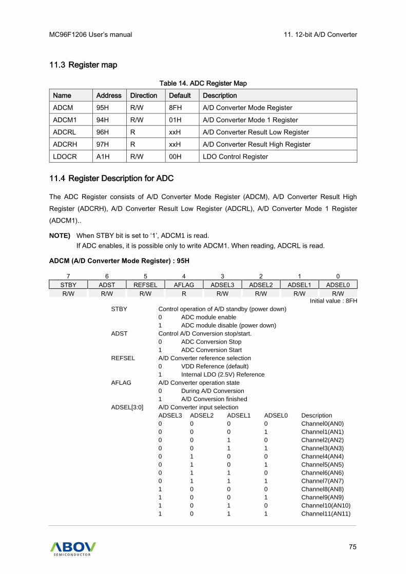
MC96F1206 User’s manual 11. 12-bit A/D Converter
75
Register map
Table 14. ADC Register Map
Name Address Direction Default Description
ADCM 95H R/W 8FH A/D Converter Mode Register
ADCM1 94H R/W 01H A/D Converter Mode 1 Register
ADCRL 96H R xxH A/D Converter Result Low Register
ADCRH 97H R xxH A/D Converter Result High Register
LDOCR A1H R/W 00H LDO Control Register
Register Description for ADC
The ADC Register consists of A/D Converter Mode Register (ADCM), A/D Converter Result High
Register (ADCRH), A/D Converter Result Low Register (ADCRL), A/D Converter Mode 1 Register
(ADCM1)..
NOTE) When STBY bit is set to ‘1’, ADCM1 is read.
If ADC enables, it is possible only to write ADCM1. When reading, ADCRL is read.
ADCM (A/D Converter Mode Register) : 95H
7 6 5 4 3 2 1 0
STBY ADST REFSEL AFLAG ADSEL3 ADSEL2 ADSEL1 ADSEL0
R/W R/W R/W R R/W R/W R/W R/W Initial value : 8FH
STBY Control operation of A/D standby (power down)
0 ADC module enable
1 ADC module disable (power down)
ADST Control A/D Conversion stop/start.
0 ADC Conversion Stop
1 ADC Conversion Start
REFSEL A/D Converter reference selection
0 VDD Reference (default)
1 Internal LDO (2.5V) Reference
AFLAG A/D Converter operation state
0 During A/D Conversion
1 A/D Conversion finished
ADSEL[3:0] A/D Converter input selection
ADSEL3 ADSEL2 ADSEL1 ADSEL0 Description
0 0 0 0 Channel0(AN0)
0 0 0 1 Channel1(AN1)
0 0 1 0 Channel2(AN2)
0 0 1 1 Channel3(AN3)
0 1 0 0 Channel4(AN4)
0 1 0 1 Channel5(AN5)
0 1 1 0 Channel6(AN6)
0 1 1 1 Channel7(AN7)
1 0 0 0 Channel8(AN8)
1 0 0 1 Channel9(AN9)
1 0 1 0 Channel10(AN10)
1 0 1 1 Channel11(AN11)

11. 12-bit A/D Converter MC96F1206 User’s manual
76
1 1 0 0 Channel12(AN12)
1 1 0 1 Channel13(AN13)
1 1 1 0 Channel14(AN14)
1 1 1 1 Channel15(BMR)
NOTE) When using ports as ADC input port, set corresponding PSR2, PSR3 register to ADC input mode in order to open analog input switch and to prevent digital input.
ADCRH (A/D Converter Result High Register) : 97H
7 6 5 4 3 2 1 0
ADDM11
ADDM10
ADDM9
ADDM8
ADDM7
ADDL11
ADDM6
ADDL10
ADDM5
ADDL9
ADDM4
ADDL8
R R R R R R R R Initial value : xxH
ADDM[11:4] MSB align, A/D Converter High result (8-bit), default
ADDL[11:8] LSB align, A/D Converter High result (4-bit)
ADCRL (A/D Converter Result Low Register) : 96H
7 6 5 4 3 2 1 0
ADDM3
ADDL7
ADDM2
ADDL6
ADDM1
ADDL5
ADDM0
ADDL4
ADDL3
ADDL2
ADDL1
ADDL0
R R R R R R R R Initial value : xxH
ADDM[3:0] MSB align, A/D Converter Low result (4-bit), default
ADDL[7:0] LSB align, A/D Converter Low result (8-bit)
ADCM1 (A/D Converter Mode Register) : 94H
7 6 5 4 3 2 1 0
EXTRG TSEL2 TSEL1 TSEL0 - ALIGN CKSEL1 CKSEL0
R/W R/W R/W R/W - R/W R/W R/W Initial value : 01H
EXTRG A/D external Trigger
0 External Trigger disable
1 External Trigger enable
TSEL[2:0] A/D Trigger Source selection
TSEL2 TSEL1 TSEL0 Description
0 0 0 Ext. Interrupt 0
0 0 1 Ext. Interrupt 1
0 1 0 -
0 1 1 -
1 0 0 Timer0 interrupt
1 0 1 Timer1 interrupt
1 1 0 -
ALIGN A/D Converter data align selection.
0 MSB align (ADCRH[7:0], ADCRL[7:4])
1 LSB align (ADCRH[3:0], ADCRL[7:0])
CKSEL[1:0] A/D Converter Clock selection
CKSEL1 CKSEL0 ADC Clock ADC VDD
0 0 fx/4 3V~5V
0 1 fx/8 3V~5V
1 0 fx/16 2.7V~3V
1 1 fx/32 2.4V~2.7V

MC96F1206 User’s manual 11. 12-bit A/D Converter
77
NOTE) fx : system clock. ADC clock should be used below 3MHz
LDOCR (LDO Control Register) : A1H
7 6 5 4 3 2 1 0
- - - - - VREF2P3SEL DSCHGEN LDOEN
- - - - - R/W R/W R/W Initial value : 00H
VREF2P3SEL
LDO output voltage select (Test only)
0 2.5V (default)
1 About 2.3V
DSCHGEN LDO Output Voltage Discharge Enable (Test only)
0 Disable
1 Enable
LDOEN 2.5V LDO Enable
0 Disable (default)
1 Enable

12. Power-down operation MC96F1206 User’s manual
78
Power down operation
The MC96F1206 has three power-down modes to minimize the power consumption of the device. In
power down mode, power consumption is reduced considerably. The device provides three kinds of
power saving functions, IDLE, STOP1 and STOP2 mode. In three modes, program is stopped.
Peripheral Operation in IDLE/STOP Mode
Peripheral’s operations during IDLE/STOP mode is introduced in table 25.
Table 15. Peripheral Operation during Power Down Mode
Peripheral IDLE Mode STOP1 Mode
STOP1 = ‘1’
STOP2 Mode
STOP1 = ‘0’
CPU ALL CPU Operation are
Disable
ALL CPU Operation are
Disable
ALL CPU Operation are
Disable
RAM Retain Retain Retain
Watch Dog
Timer Operates Continuously Operates Continuously Stop
Timer Operates Continuously
Halted (Only when the Event
Counter Mode is Enable, Timer
operates Normally)
Halted (Only when the Event
Counter Mode is Enable, Timer
operates Normally)
Internal OSC
(32MHz) Oscillation Stop Stop
Internal
WDTOSC
(8kHz)
Oscillation Oscillation Stop
I/O Port Retain Retain Retain
Control
Register Retain Retain Retain
Address Data
Bus Retain Retain Retain
Release
Method By RESET, all Interrupts
By RESET, External Interrupt,
WDT, LVI, TIMER(EC)
By RESET, External Interrupt,
LVI, TIMER(EC)
NOTE) Before you use MCU STOP1/2 mode, you must disable P02, P13 debounce.

MC96F1206 User’s manual 12. Power-down operation
79
IDLE mode
The power control register is set to ‘01h’ to enter the IDLE Mode. In this mode, the internal oscillation
circuits remain active. Oscillation continues and peripherals are operated normally but CPU stops. It is
released by reset or interrupt. To be released by interrupt, interrupt should be enabled before IDLE
mode. If using reset, because the device becomes initialized state, the registers have reset value.
Figure 40. IDLE Mode Release Timing by External Interrupt
(Ex) MOV PCON, #0000_0001b ; setting of IDLE mode : set the bit of STOP and IDLE Control
register (PCON)
STOP mode
The power control register is set to ‘03h’ to enter the STOP Mode. In the stop mode, the main oscillator,
system clock and peripheral clock is stopped, but watch timer continue to operate if STOP1 bit in SCCR
register is written to ‘1’. With the clock frozen, all functions are stopped, but the on-chip RAM and control
registers are held.
The source for exit from STOP mode is hardware reset and interrupts. The reset re-defines all the
control registers.
When exit from STOP mode, enough oscillation stabilization time is required to normal operation. It is
proportional to the system clock.
Oscillation stabilization time = Default 16ms @ 8kHz WDTRC

12. Power-down operation MC96F1206 User’s manual
80
Figure 41. STOP Mode Release Timing by External Interrupt
Release operation of STOP1,2 mode
After STOP1, 2 mode is released, the operation begins according to content of related interrupt register
just before STOP1, 2 mode start (Figure 42). Interrupt Enable Flag of All (EA) of IE should be set to `1`.
Released by only interrupt which each interrupt enable flag = `1`, and jump to the relevant interrupt
service routine
Figure 42. STOP Mode Release Flow

MC96F1206 User’s manual 12. Power-down operation
81
Register Map and Register Description for Power Down Operation
Table 16. Power-down Operation Register Map
Name Address Direction Default Description
PCON 87H R/W 00H Power control register
Register description
PCON (Power Control Register): 87H
7 6 5 4 3 2 1 0
bit 7 bit 6 bit 5 bit 4 bit 3 bit 2 bit 1 bit 0
R/W R/W R/W R/W R/W R/W R/W R/W
Initial value: 00H
01H IDLE mode enable
03H STOP1, 2 mode enable
NOTE)
1. To enter IDLE mode, PCON must be set to ‘01H’.
2. To STOP1, 2 mode, PCON must be set to ‘03H’.
(In STOP1, 2 mode, PCON register is cleared automatically by interrupt or reset)
3. When PCON is set to ‘03H’, if STOP1 (in the SCCR register) is set to ‘1’, it enters the STOP1
mode. if
4. STOP1 is cleared to ‘0’, it enters the STOP2 mode
5. The different thing in STOP 1, 2 is only clock operation of internal 8 kHz-WDTOSC during
STOP mode operating
Table 17. Example Code with 3 or more NOP Instructions
Example code 1 Example code 2
MOV PCON, #01H ; IDLE mode
NOP
NOP
NOP
MOV PCON, #03H ; STOP mode
NOP
NOP
NOP

13. Reset MC96F1206 User’s manual
82
Reset
The MC96F1206 has reset by external RESETB pin. The following is the hardware setting value.
Table 18. Reset Value and the Relevant On Chip Hardware
On Chip Hardware Reset Value
Program Counter (PC) 0000H
Accumulator 00H
Stack Pointer (SP) 07H
Peripheral clock On
Control register Refer to peripheral registers.
Low Voltage Indicator Enable
The MC96F1206 has six types of reset generation procedures. The following is the reset sources.
- External RESETB
- Power ON RESET (POR)
- WDT Overflow Reset (In the case of WDT_EN = ‘1’)
- LVR Reset
- OCD Reset
- LVI Reset (In the case of LVILS ≠ ‘000’)
Reset block diagram
WDT RST
WDT RSTEN
Ext RESET
Disable by FUSE
RESET Noise
Canceller
LVI_OUT
LVI Enable RESET Noise
Canceller
POR RST
LVR RST
LVROFF
RESETB
Figure 43. Reset Block Diagram
Power on Reset
When rising device power, the POR (Power ON Reset) have a function to reset the device. If using
POR, it executes the device RESET function instead of the RESET IC or the RESET circuits. And
External RESET PIN is able to use as Normal I/O pin.
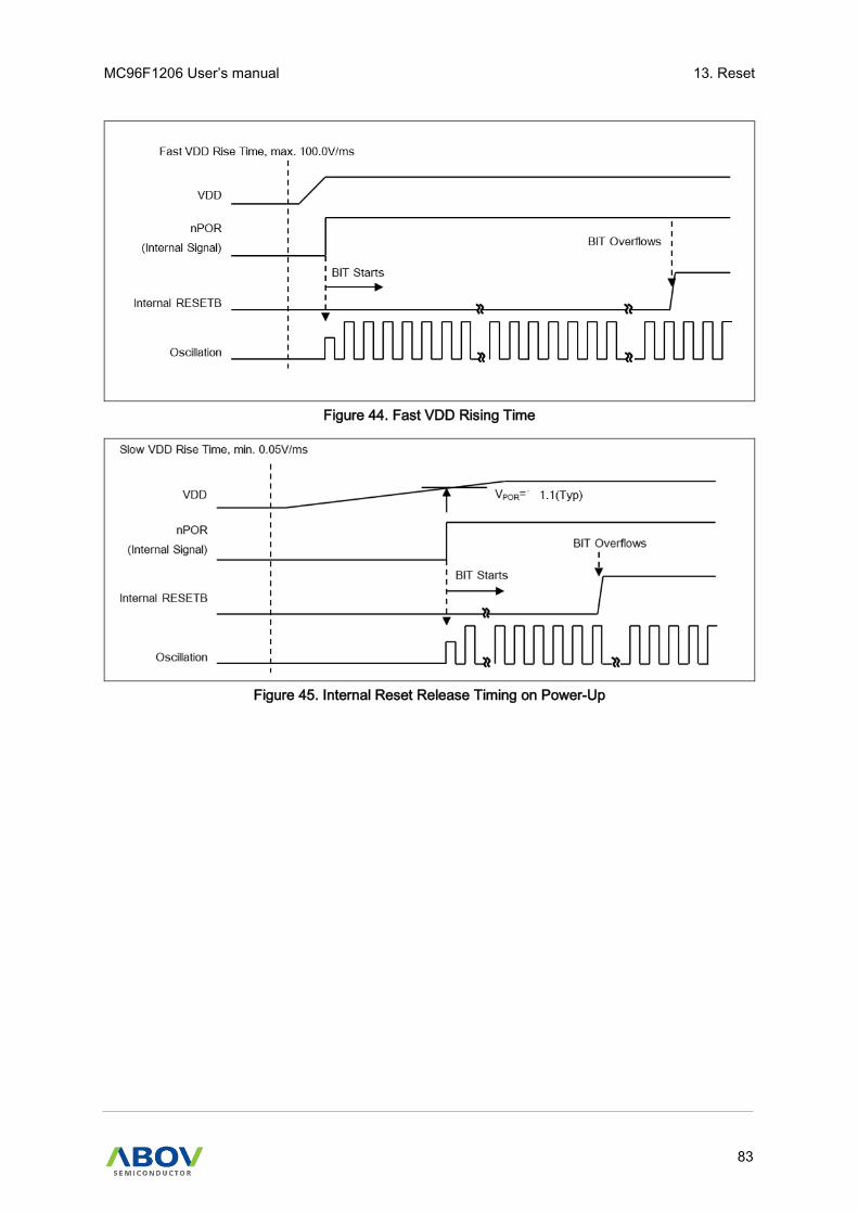
MC96F1206 User’s manual 13. Reset
83
Figure 44. Fast VDD Rising Time
Figure 45. Internal Reset Release Timing on Power-Up

13. Reset MC96F1206 User’s manual
84
Figure 46. Configuration Timing when Power-On
Relationship between VDD input and internal oscillator is described in figure 47 and table 19.
Figure 47. Boot Process Waveform
Default 16ms @ WDTRC 8kHz
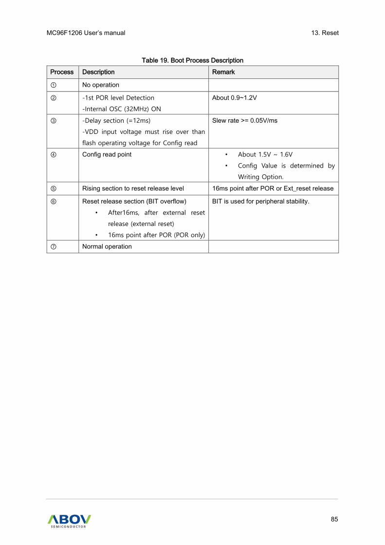
MC96F1206 User’s manual 13. Reset
85
Table 19. Boot Process Description
Process Description Remark
① No operation
② -1st POR level Detection
-Internal OSC (32MHz) ON
About 0.9~1.2V
③ -Delay section (=12ms)
-VDD input voltage must rise over than
flash operating voltage for Config read
Slew rate >= 0.05V/ms
④ Config read point • About 1.5V ~ 1.6V
• Config Value is determined by
Writing Option.
⑤ Rising section to reset release level 16ms point after POR or Ext_reset release
⑥ Reset release section (BIT overflow)
• After16ms, after external reset
release (external reset)
• 16ms point after POR (POR only)
BIT is used for peripheral stability.
⑦ Normal operation

13. Reset MC96F1206 User’s manual
86
External RESETB input
The External RESETB is the input to a Schmitt trigger. A reset in accomplished by holding the reset pin
low for at least 10us over, within the operating voltage range and oscillation stable, it is applied, and the
internal state is initialized. After reset state becomes ‘1’, it needs the stabilization time with default 16ms
and after the stable state, the internal RESET becomes ‘1’. And the program execution starts at the
vector address stored at address 0000H.
The Figure 49 is the Noise canceller time diagram. It has the Noise cancel value of about 500us
(@VDD=5V) to the low input of System Reset.
Figure 48. Timing Diagram after RESET
Figure 49. Reset noise canceller time diagram
Default 16ms @ WDTRC 8kHz

MC96F1206 User’s manual 13. Reset
87
NOTES:
1. Stable generating time is not included in the start-up time.
2. RESETB pin has a pull-up resistor by H/W.
Figure 50. Oscillator Generating Waveform Example
Low Voltage Indicator Processor
The MC96F1206 has an On-chip Low Voltage Indicator circuit for monitoring the VDD level during
operation by comparing it to a fixed trigger level. The trigger level for the LVI can be selected by
LVILS[2:0]. In the STOP mode, this will contribute significantly to the total current consumption. So to
minimize the current consumption, the LVILS[2:0] is set to off by software.
13.4.1 Block diagram
Low Voltage
Indicator
(LVI)
External VDD
2.1V
2.5V
3.5V
LVILS[2:0]
De-bounce Clock
LVILS[2:0] ≠ 0
CP
D Q
1
0
STOP1/2 mode
LVIRF LVI reset
LVIIF LVI interrupt
Figure 51. LVI Block Diagram

13. Reset MC96F1206 User’s manual
88
13.4.2 Internal reset and LVD reset in timing diagram
Figure 52. Internal Reset at Power Fail Situation
Register map
Table 20. Reset Operation Register Map
Name Address Direction Default Description
RSFR 86H R/W 84H Reset Source Flag Register
LVIR 8FH R/W 40H LVI Control Register
Register description
RSFR (Reset Source Flag Register) : 86H
7 6 5 4 3 2 1 0
PORF EXTRF WDTRF OCDRF LVIRF LVRRF - -
R/W R/W R/W R/W R/W R/W - - Initial value : C4H
PORF Power-On Reset flag bit. The bit is reset by writing ‘0’ to this bit.
0 No detection
1 Detection
EXTRF External Reset flag bit. The bit is reset by writing ‘0’ to this bit or by
Power ON reset.
0 No detection
1 Detection
WDTRF Watch Dog Reset flag bit. The bit is reset by writing ‘0’ to this bit or by
Power ON reset.
0 No detection
1 Detection
OCDRF On-Chip Debug Reset flag bit. The bit is reset by writing ‘0’ to this bit or
by Power ON reset.
0 No detection
1 Detection
LVIRF Low Voltage Indicator Reset flag bit. The bit is reset by writing ‘0’ to this
bit or by Power ON reset.
0 No detection
1 Detection
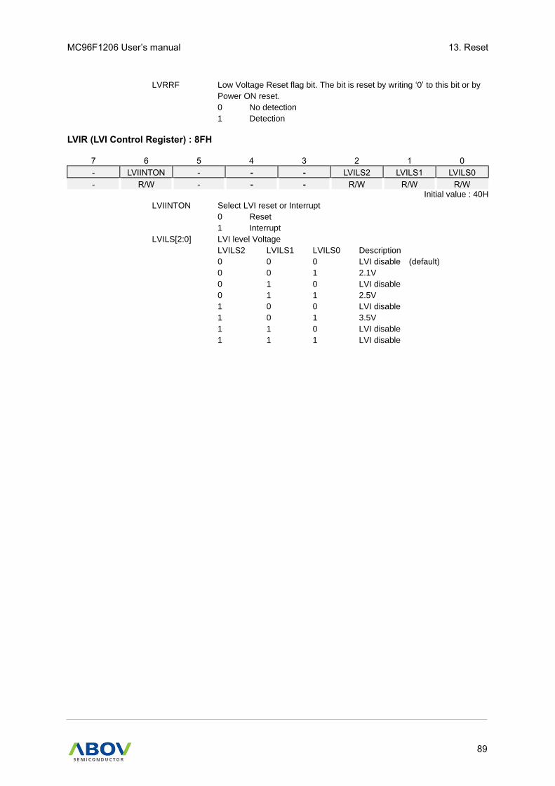
MC96F1206 User’s manual 13. Reset
89
LVRRF Low Voltage Reset flag bit. The bit is reset by writing ‘0’ to this bit or by
Power ON reset.
0 No detection
1 Detection
LVIR (LVI Control Register) : 8FH
7 6 5 4 3 2 1 0
- LVIINTON - - - LVILS2 LVILS1 LVILS0
- R/W - - - R/W R/W R/W Initial value : 40H
LVIINTON Select LVI reset or Interrupt
0 Reset
1 Interrupt
LVILS[2:0] LVI level Voltage
LVILS2 LVILS1 LVILS0 Description
0 0 0 LVI disable (default)
0 0 1 2.1V
0 1 0 LVI disable
0 1 1 2.5V
1 0 0 LVI disable
1 0 1 3.5V
1 1 0 LVI disable
1 1 1 LVI disable

14. Flash memory MC96F1206 User’s manual
90
Flash memory
MC96F1206 incorporates flash memory inside. Program can be written, erased, and overwritten on the
flash memory while it is mounted on a board. The flash memory can be read by ‘MOVC’ instruction and
programmed in OCD, serial ISP mode or user program mode. Followings are features summary of flash
memory.
• Flash Size : 6Kbytes
• Single power supply program and erase
• Command interface for fast program and erase operation
• Up to 10,000 program/erase cycles at typical voltage and temperature for flash memory

MC96F1206 User’s manual 14. Flash Memory
91
Flash program ROM structure
Figure 53. Flash Memory Map
Figure 54.Address configuration of Flash memory

14. Flash memory MC96F1206 User’s manual
92
Register map
Table 21. Flash Memory Register Map
Name Address Direction Default Description
FEMR EAH R/W 00H Flash Mode Register
FECR EBH R/W 03H Flash Control Register
FESR ECH R/W 80H Flash Status Register
FETCR EDH R/W 00H Flash Time Control Register
FEARL F2H R/W 00H Flash Address Low Register
FEARM F3H R/W 00H Flash Address Middle Register
FEARH F4H R/W 00H Flash Address High Register
Register description
FEMR (Flash Mode Register) : EAH
7 6 5 4 3 2 1 0
FSEL - PGM ERASE PBUFF OTPE VFY FEEN
R/W - R/W R/W R/W R/W R/W R/W Initial value : 00H
FSEL Select flash memory.
0 Deselect flash memory
1 Select flash memory
PGM Enable program or program verify mode with VFY
0 Disable program or program verify mode
1 Enable program or program verify mode
ERASE Enable erase or erase verify mode with VFY
0 Disable erase or erase verify mode
1 Enable erase or erase verify mode
PBUFF Select page buffer
0 Deselect page buffer
1 Select page buffer
OTPE Select OTP area instead of program memory
0 Deselect OTP area
1 Select OTP area
VFY Set program or erase verify mode with PGM or ERASE
Program Verify: PGM=1, VFY=1
Erase Verify: ERASE=1, VFY=1
FEEN Enable program and erase of Flash. When inactive, it is possible to read
as normal mode
0 Disable program and erase
1 Enable program and erase
FEARL (Flash address low Register) : F2H
7 6 5 4 3 2 1 0
ARL7 ARL6 ARL5 ARL4 ARL3 ARL2 ARL1 ARL0
W W W W W W W W

MC96F1206 User’s manual 14. Flash Memory
93
Initial value : 00H
ARL[7:0] Flash address low
FECR (Flash Control Register) : EBH
7 6 5 4 3 2 1 0
AEF - EXIT1 EXIT0 WRITE READ nFERST nPBRST
R/W - R/W R/W R/W R/W R/W R/W Initial value : 03H
AEF Enable flash bulk erase mode
0 Disable bulk erase mode of Flash memory
1 Enable bulk erase mode of Flash memory
EXIT[1:0] Exit from program mode. It is cleared automatically after 1 clock
EXIT1 EXIT0 Description
0 0 Don’t exit from program mode
0 1 Don’t exit from program mode
1 0 Don’t exit from program mode
1 1 Exit from program mode
WRITE Start to program or erase of Flash. It is cleared automatically after 1 clock
0 No operation
1 Start to program or erase of Flash
READ Start auto-verify of Flash. It is cleared automatically after 1 clock
0 No operation
1 Start auto-verify of Flash
nFERST Reset Flash control logic. It is cleared automatically after 1 clock
0 No operation
1 Reset Flash control logic.
nPBRST Reset page buffer with PBUFF. It is cleared automatically after 1 clock
PBUFF nPBRST Description
0 0 Page buffer reset
1 0 Write checksum reset
WRITE and READ bits can be used in program, erase and verify mode with FEAR registers. Read or
writes for memory cell or page buffer uses read and write enable signals from memory controller.
Indirect address mode with FEAR is only allowed to program, erase and verify
FESR (Flash Status Register) : ECH
7 6 5 4 3 2 1 0
PEVBSY VFYGOOD - - ROMINT WMODE EMODE VMODE
R R/W R R R/W R R R Initial value : 80H
PEVBSY
Operation status flag. It is cleared automatically when operation starts.
Operations are program, erase or verification
0 Busy (Operation processing)
1 Complete Operation
VFYGOOD Auto-verification result flag.
0 Auto-verification fails
1 Auto-verification successes
ROMINT Flash interrupt request flag. Auto-cleared when program/erase/verify
starts. Active in program/erase/verify completion
0 No interrupt request.
1 Interrupt request.
WMODE Write mode flag
EMODE Erase mode flag

14. Flash memory MC96F1206 User’s manual
94
VMODE Verify mode flag
FEARM (Flash address middle Register) : F3H
7 6 5 4 3 2 1 0
ARM7 ARM6 ARM5 ARM4 ARM3 ARM2 ARM1 ARM0
W W W W W W W W Initial value : 00H
ARM[7:0] Flash address middle
FEARH (Flash address high Register) : F4H
7 6 5 4 3 2 1 0
ARH7 ARH6 ARH5 ARH4 ARH3 ARH2 ARH1 ARH0
W W W W W W W W Initial value : 00H
ARH[7:0] Flash address high
FEAR registers are used for program, erase and auto-verify. In program and erase mode, it is page
address and ignored the same least significant bits as the number of bits of page address. In auto-verify
mode, address increases automatically by one. FEARs are write-only register. Reading these registers
returns 24-bit checksum result
FETCR (Flash Time control Register) : EDH
7 6 5 4 3 2 1 0
TCR7 TCR6 TCR5 TCR4 TCR3 TCR2 TCR1 TCR0
R/W R/W R/W R/W R/W R/W R/W R/W Initial value : 00H
TCR[7:0] Flash Time control
Program and erase time is controlled by setting FETCR register. Program and erase timer uses 10-bit
counter. It increases by one at each divided system clock frequency(=SCLK/128). It is cleared when
program or erase starts. Timer stops when 10-bit counter is same to FETCR. PEVBSY is cleared when
program, erase or verify starts and set when program, erase or verify stops. Max program/erase time
at 16Mhz system clock : (255+1) * 2 * (62.5ns * 128) = 4.096ms
In the case of 10% of error rate of counter source clock, program or erase time is 3.6~4.5ms
Program/erase time calculation
for page write or erase, Tpe = (TCON+1) * 2 * (SCLK * 128)
for bulk erase, Tbe = (TCON+1) * 4 * (SCLK * 128)
Table 22. Program/erase Time
Min Typ Max Unit
program/erase Time 2.4 2.5 2.6 ms
※ Recommended program/erase time at 16MHz (FETCR = 9Dh)

MC96F1206 User’s manual 14. Flash Memory
95
Serial In-System Program (ISP) mode
Serial in-system program uses the interface of debugger which uses two wires. Refer to Chapter 16.
Development tools in details about debugger.
14.4.1 Flash operation
Configuration (This Configuration is just used for follow description)
7 6 5 4 3 2 1 0
- FEMR[4]&[1] FEMR[5]&[1] - - FEMR[2] FECR[6] FECR[7]
- ERASE&VFY PGM&VFY - - OTPE AEE AEF
Figure 55.The sequence of page program and erase of Flash memory
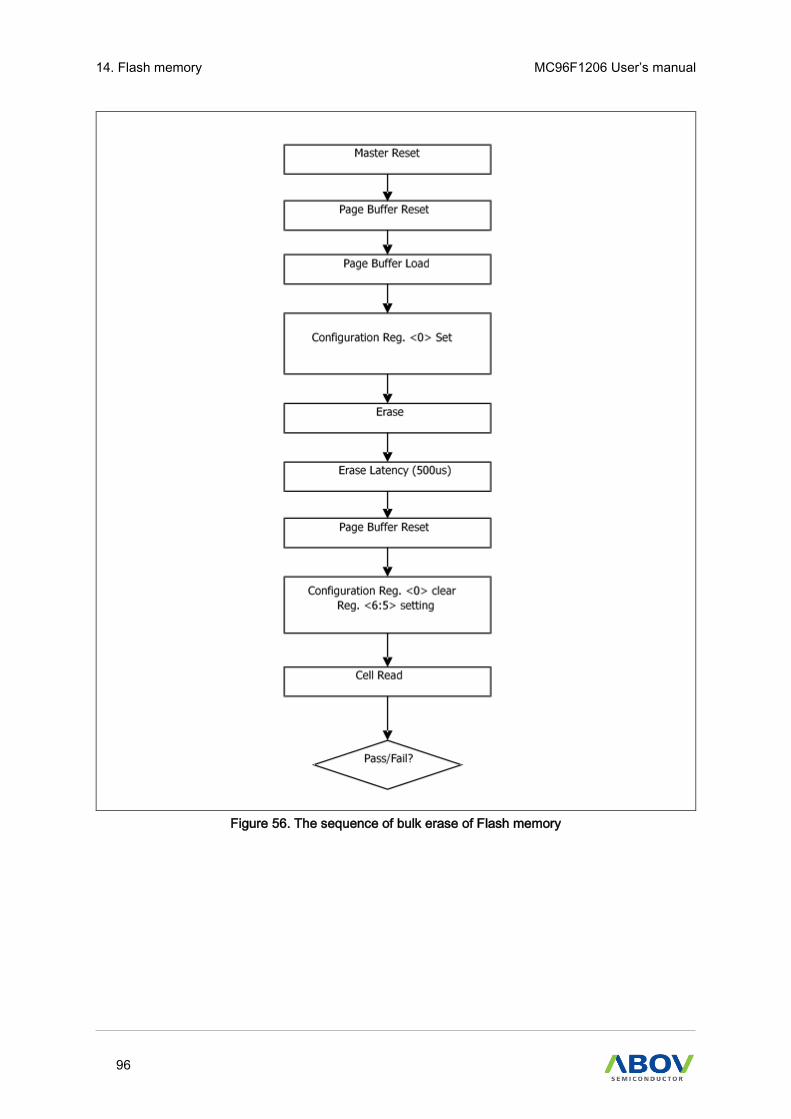
14. Flash memory MC96F1206 User’s manual
96
Figure 56. The sequence of bulk erase of Flash memory

MC96F1206 User’s manual 14. Flash Memory
97
14.4.2 Flash Read
Step 1. Enter OCD(=ISP) mode.
Step 2. Set ENBDM bit of BCR.
Step 3. Enable debug and Request debug mode.
Step 4. Read data from Flash.
14.4.3 Enable program mode
Step 1. Enter OCD(=ISP) mode.1
Step 2. Set ENBDM bit of BCR.
Step 3. Enable debug and Request debug mode.
Step 4. Enter program/erase mode sequence.2
(1) Write 0xAA to 0xF555.
(2) Write 0x55 to 0xFAAA.
(3) Write 0xA5 to 0xF555.
1 Refer to how to enter ISP mode..
2 Command sequence to activate Flash write/erase mode. It is composed of sequentially writing data
of Flash memory.
14.4.4 Flash write mode
Step 1. Enable program mode.
Step 2. Reset page buffer. FEMR: 1000_0001 FECR:0000_0010
Step 3. Select page buffer. FEMR:1000_1001
Step 4. Write data to page buffer.(Address automatically increases by twin.)
Step 5. Set write mode. FEMR:1010_0001
Step 6. Set page address. FEARH:FEARM:FEARL=20’hx_xxxx
Step 7. Set FETCR.
Step 8. Start program. FECR:0000_1011
Step 9. Insert one NOP operation
Step 10. Read FESR until PEVBSY is 1.
Step 11. Repeat step2 to step 8 until all pages are written.

14. Flash memory MC96F1206 User’s manual
98
14.4.5 Flash page erase mode
Step 1. Enable program mode.
Step 2. Reset page buffer. FEMR: 1000_0001 FECR:0000_0010
Step 3. Select page buffer. FEMR:1000_1001
Step 4. Write ‘h00 to page buffer. (Data value is not important.)
Step 5. Set erase mode. FEMR:1001_0001
Step 6. Set page address. FEARH:FEARM:FEARL=20’hx_xxxx
Step 7. Set FETCR.
Step 8. Start erase. FECR:0000_1011
Step 9. Insert one NOP operation
Step 10. Read FESR until PEVBSY is 1.
Step 11. Repeat step2 to step 8 until all pages are erased.
14.4.6 Flash bulk erase mode
Step 1. Enable program mode.
Step 2. Reset page buffer. FEMR: 1000_0001 FECR:0000_0010
Step 3. Select page buffer. FEMR:1000_1001
Step 4. Write ‘h00 to page buffer. (Data value is not important.)
Step 5. Set erase mode. FEMR:1001_0001.
(Only main cell area is erased. For bulk erase including OTP area, select OTP area.(set FEMR to
1000_1101.)
Step 6. Set FETCR
Step 7. Start bulk erase. FECR:1000_1011
Step 8. Insert one NOP operation
Step 9. Read FESR until PEVBSY is 1.
14.4.7 Flash OTP area read mode
Step 1. Enter OCD(=ISP) mode.
Step 2. Set ENBDM bit of BCR.
Step 3. Enable debug and Request debug mode.
Step 4. Select OTP area. FEMR:1000_0101
Step 5. Read data from Flash.

MC96F1206 User’s manual 14. Flash Memory
99
14.4.8 Flash OTP area write mode
Step 1. Enable program mode.
Step 2. Reset page buffer. FEMR: 1000_0001 FECR:0000_0010
Step 3. Select page buffer. FEMR:1000_1001
Step 4. Write data to page buffer.(Address automatically increases by twin.)
Step 5. Set write mode and select OTP area. FEMR:1010_0101
Step 6. Set page address. FEARH:FEARM:FEARL=20’hx_xxxx
Step 7. Set FETCR.
Step 8. Start program. FECR:0000_1011
Step 9. Insert one NOP operation
Step 10. Read FESR until PEVBSY is 1.
14.4.9 Flash OTP area erase mode
Step 1. Enable program mode.
Step 2. Reset page buffer. FEMR: 1000_0001 FECR:0000_0010
Step 3. Select page buffer. FEMR:1000_1001
Step 4. Write ‘h00 to page buffer. (Data value is not important.)
Step 5. Set erase mode and select OTP area. FEMR:1001_0101
Step 6. Set page address. FEARH:FEARM:FEARL=20’hx_xxxx
Step 7. Set FETCR.
Step 8. Start erase. FECR:0000_1011
Step 9. Insert one NOP operation
Step 10. Read FESR until PEVBSY is 1.
14.4.10 Flash program verify mode
Step 1. Enable program mode.
Step 2. Set program verify mode. FEMR:1010_0011
Step 3. Read data from Flash.
14.4.11 Flash program verify mode
Step 1. Enable program mode.
Step 2. Set program verify mode. FEMR:1010_0011
Step 3. Read data from Flash.

14. Flash memory MC96F1206 User’s manual
100
14.4.12 OTP program verify mode
Step 1. Enable program mode.
Step 2. Set program verify mode. FEMR:1010_0111
Step 3. Read data from Flash.
14.4.13 Flash erase verify mode
Step 1. Enable program mode.
Step 2. Set erase verify mode. FEMR:1001_0011
Step 3. Read data from Flash.
14.4.14 Flash page buffer read
Step 1. Enable program mode.
Step 2. Select page buffer. FEMR:1000_1001
Step 3. Read data from Flash.
Summary of Flash Program/Erase Mode
Table 23.Operation Mode
Operation mode Description
F
L
A
S
H
Flash read Read cell by byte.
Flash write Write cell by bytes or page.
Flash page erase Erase cell by page.
Flash bulk erase Erase the whole cells.
Flash program verify Read cell in verify mode after programming.
Flash erase verify Read cell in verify mode after erase.
Flash page buffer load Load data to page buffer.
Security
MC96F1206 provides Lock bits which can be left unprogrammed (“0”) or can be programmed (“1”) to
obtain the additional features listed in
24. The Lock bits can be erased to “0” with only the bulk erase command and a value of more than
0x80 at FETCR.

MC96F1206 User’s manual 14. Flash Memory
101
Table 24.Security policy using lock-bits
LOCK
MODE
USER MODE ISP/PMODE
FLASH OTP FLASH OTP
LOCKF R W PE BE R W PE BE R W PE BE R W PE BE
0 O O O X X X X X O O O O O O O O
1 O O O X X X X X X X X O O X X O
LOCKF: Lock bit of Flash memory
R: Read
W: Write
PE: Page erase
BE: Bulk Erase
O: Operation is possible.
X: Operation is impossible.

15. Electrical characteristics MC96F1206 User’s manual
102
Electrical characteristics
Absolute maximum ratings
Table 25.Absolute Maximum Ratings
Parameter Sym
bol Rating Unit Note
Supply Voltage VDD -0.3~+6.5 V –
Normal Voltage Pin
VI -0.3~VDD+0.3 V Voltage on any pin with respect to VSS
VO -0.3~VDD+0.3 V
IOH -15 mA Maximum current output sourced by (IOH per
I/O pin)
∑IOH -80 mA Maximum current (∑IOH)
IOL 30 mA Maximum current sunk by (IOL per I/O pin)
∑IOL 160 mA Maximum current (∑IOL)
Total Power Dissipation PT 400 mW –
Storage Temperature TSTG -65~+150 °C –
Caution Stresses beyond those listed under ‘Absolute Maximum Ratings’ may cause permanent damage to the device. This is a
stress rating only and functional operation of the device at those or any other conditions above those indicated in the operation listings of this specification is not implied. Exposure above maximum rating conditions for extended periods may
affect device reliability.
Recommended Operating Conditions
(TA=-40°C ~ +85°C)
Table 26.Recommended Operating Conditions
Parameter Symbol Conditions MIN TYP MAX Unit
Operating Voltage VDD fX= 1, 4, 8,
16MHz Internal RC 2.2 – 5.5 V
Operating
Temperature TOPR VDD=2.2~5.5V -40 – 85 °C
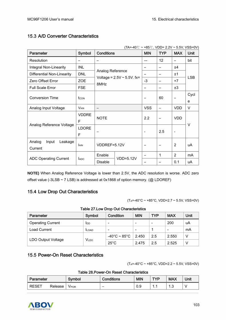
MC96F1206 User’s manual 15. Electrical characteristics
103
A/D Converter Characteristics
(TA=-40 ~ +85, VDD= 2.2V ~ 5.5V, VSS=0V)
Parameter Symbol Conditions MIN TYP MAX Unit
Resolution – – –- 12 – bit
Integral Non-Linearity INL Analog Reference
Voltage = 2.5V ~ 5.5V. fx=
8MHz
– – ±4
LSB Differential Non-Linearity DNL – – ±1
Zero Offset Error ZOE -3 – +7
Full Scale Error FSE – – ±3
Conversion Time tCON – 60 – Cycl
e
Analog Input Voltage VAIN – VSS – VDD V
Analog Reference Voltage
VDDRE
F NOTE 2.2 – VDD
V LDORE
F – - 2.5 -
Analog Input Leakage
Current IAIN VDDREF=5.12V – – 2 uA
ADC Operating Current IADC Enable
VDD=5.12V – 1 2 mA
Disable – – 0.1 uA
NOTE) When Analog Reference Voltage is lower than 2.5V, the ADC resolution is worse. ADC zero
offset value (-3LSB ~ 7 LSB) is addressed at 0x1868 of option memory. (@ LDOREF)
Low Drop Out Characteristics
(TA=-40°C ~ +85°C, VDD=2.7 ~ 5.5V, VSS=0V)
Table 27.Low Drop Out Characteristics
Parameter Symbol Condition MIN TYP MAX Unit
Operating Current IDD - - - 200 uA
Load Current ILOAD - - 1 - mA
LDO Output Voltage VLDO -40°C ~ 85°C 2.450 2.5 2.550 V
25°C 2.475 2.5 2.525 V
Power-On Reset Characteristics
(TA=-40°C ~ +85°C, VDD=2.2 ~ 5.5V, VSS=0V)
Table 28.Power-On Reset Characteristics
Parameter Symbol Conditions MIN TYP MAX Unit
RESET Release VPOR – 0.9 1.1 1.3 V
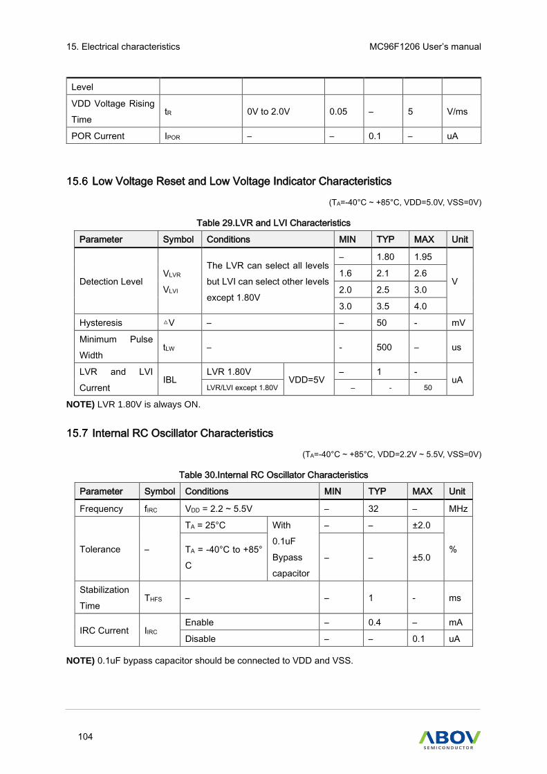
15. Electrical characteristics MC96F1206 User’s manual
104
Level
VDD Voltage Rising
Time tR 0V to 2.0V 0.05 – 5 V/ms
POR Current IPOR – – 0.1 – uA
Low Voltage Reset and Low Voltage Indicator Characteristics
(TA=-40°C ~ +85°C, VDD=5.0V, VSS=0V)
Table 29.LVR and LVI Characteristics
Parameter Symbol Conditions MIN TYP MAX Unit
Detection Level VLVR
VLVI
The LVR can select all levels
but LVI can select other levels
except 1.80V
– 1.80 1.95
V 1.6 2.1 2.6
2.0 2.5 3.0
3.0 3.5 4.0
Hysteresis V – – 50 - mV
Minimum Pulse
Width tLW – - 500 – us
LVR and LVI
Current IBL
LVR 1.80V VDD=5V
– 1 - uA
LVR/LVI except 1.80V – - 50
NOTE) LVR 1.80V is always ON.
Internal RC Oscillator Characteristics
(TA=-40°C ~ +85°C, VDD=2.2V ~ 5.5V, VSS=0V)
Table 30.Internal RC Oscillator Characteristics
Parameter Symbol Conditions MIN TYP MAX Unit
Frequency fIRC VDD = 2.2 ~ 5.5V – 32 – MHz
Tolerance –
TA = 25°C With
0.1uF
Bypass
capacitor
– – ±2.0
% TA = -40°C to +85°
C – – ±5.0
Stabilization
Time THFS – – 1 - ms
IRC Current IIRC Enable – 0.4 – mA
Disable – – 0.1 uA
NOTE) 0.1uF bypass capacitor should be connected to VDD and VSS.

MC96F1206 User’s manual 15. Electrical characteristics
105
Internal WDT Oscillator Characteristics
(TA=-40°C ~ +85°C, VDD=2.2V ~ 5.5V, VSS=0V)
Table 31.Internal WDT Oscillator Characteristics
Parameter Symbol Conditions MIN TYP MAX Unit
Frequency fWDTRC – 4 8 12 kHz
Stabilization Time tWDTS – – 1 - ms
WDTRC Current IWDTRC Enable – 5 –
uA Disable – – 0.1
DC Characteristics
(TA=-40°C ~ +85°C, VDD=2.2V ~ 5.5V, VSS=0V, fX=8.0MHz)
Table 32.DC Characteristics
Parameter Symbol Conditions MIN TYP MAX Unit
VIH1 P0, P1, P2 0.8VDD – VDD V
Input Low Voltage VIL1 P0, P1, P2 – – 0.2VDD V
Output High
Voltage
VOH1 VDD=3.3V, IOH=-5mA,
All output ports VDD-1.5 – – V
VOH2 VDD=5V, IOH=-10mA,
All output ports VDD-1.5 – – V
Output Low
Voltage VOL IOL= 20mA,All output ports – – 1.0 V
Input High
Leakage
Current
IIH All input ports -1 – 1 uA
Input Low Leakage
Current IIL All input ports -1 – 1 uA
Pull-Up Resistor RPU1 VI=0V, TA= 25°C
All Input ports 25 50 100 kΩ
Supply Current
IDD1
(RUN) Run Mode, fX=8 MHz - 3 5 mA
IIDD2
(IDLE) IDLE Mode, fX=8 MHz - 2 5 mA
IDD3
(STOP1)
STOP1 Mode, WDTRC
Enable - 2 35 uA
IDD4
(STOP2)
STOP2 Mode, WDTRC
Disable - 1.5 30 uA
NOTE) STOP1: WDT only running, STOP2: All function disable.
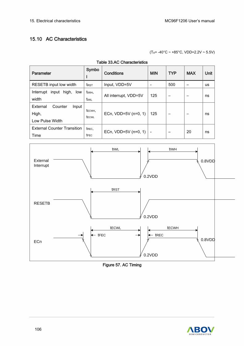
15. Electrical characteristics MC96F1206 User’s manual
106
AC Characteristics
(TA= -40°C ~ +85°C, VDD=2.2V ~ 5.5V)
Table 33.AC Characteristics
Parameter Symbo
l Conditions MIN TYP MAX Unit
RESETB input low width tRST Input, VDD=5V - 500 – us
Interrupt input high, low
width
tIWH,
tIWL All interrupt, VDD=5V 125 – – ns
External Counter Input
High,
Low Pulse Width
tECWH,
tECWL
ECn, VDD=5V (n=0, 1) 125 – – ns
External Counter Transition
Time
tREC,
tFEC
ECn, VDD=5V (n=0, 1) - – 20 ns
tIWHtIWL
External
Interrupt
tRST
0.2VDD
0.2VDD
0.8VDD
RESETB
tECWHtECWL
ECn
0.2VDD
0.8VDDtFEC tREC
Figure 57. AC Timing

MC96F1206 User’s manual 15. Electrical characteristics
107
Operating Voltage Range
2.2
1 MHz
5.5
16 MHz
(fX=1, 4, 8, 16 MHz)
Supply voltage (V)
Figure 58. Operating Voltage Range
Typical Characteristics
These graphs and tables provided in this section are for design guidance only and are not tested or
guaranteed. In some graphs or tables the data presented are outside specified operating range (e.g.
outside specified VDD range). This is for information only and devices are guaranteed to operate
properly only within the specified range.
The data presented in this section is a statistical summary of data collected on units from different lots
over a period of time. “Typical” represents the mean of the distribution while “max” or “min” represents
(mean + 3σ) and (mean - 3σ) respectively where σ is standard deviation.
Figure 59. Output Low Voltage(VOL)
Figure 60. Output High Voltage (VOH1)

15. Electrical characteristics MC96F1206 User’s manual
108
Figure 61. Output High Voltage (VOH2)
Figure 62.Power Supply Current (RUN, IDLE)
Figure 63. Power Supply Current (STOP1,
STOP2)
Figure 64. IRC Tolerance
Recommended Application Circuit
For the microprocessor and other devices in the system to function correctly, it is also necessary to
monitor the supply voltage during operations. Voltage drops or glitches on the power supply lines, can
cause unwanted changes in the internal registers, which can lead to instructions being incorrectly
executed, incorrect output signals and errors in the operations results. If noise is applied to the VDD
rising slope due to external factors during the POR, the microprocessor may malfunction because the
microprocessor continues to operate and does not recognize that the voltage has fallen below the
threshold due to the internal RC time constants. Therefore, VDD / GND requires a power capacitor for
VDD drop and a decoupling capacitor for high frequency noise. Normally, electrolytic / tantalum
capacitors of 10uf / 9V or more are recommended for power capacitors and multilayer ceramic
capacitors of 0.1uF or more are recommended for decoupling capacitors. Decoupling capacitors should
be placed as close as possible to the microprocessor.

MC96F1206 User’s manual 15. Electrical characteristics
109
Dev
ice
VSS
VDD0.1uF
+0.1uF
VDD VCC
DC Power
This 0.1uF capacitor should be within 1cm from the VDD pin of MCU on the PCB layout.
The MCU power line (VDD and VSS) should be separated from the high-current part at a DC power node on the PCB layout.
Figure 65. Recommended Power Circuit part when using DC Power.

16. Development tools MC96F1206 User’s manual
110
Development tools
This chapter introduces wide range of development tools for MC96F1206. ABOV offers software tools,
debuggers, and programmers to help a user in generating right results to match target applications.
ABOV supports entire development ecosystem of the customers.
Compiler
ABOV semiconductor does not provide any compiler for MC96F1206. However, since MC96F1206 has
Mentor 8051 as its CPU core, you can use all kinds of third party's standard 8051 compiler such as Keil
C Compiler. These compilers' output debug information can be integrated with our OCD emulator and
debugger. Please visit our website www.abovsemi.com for more information regarding the OCD
emulator and debugger.
OCD (On-Chip Debugger) emulator and debugger
The OCD emulator supports ABOV Semiconductor’s 8051 series MCU emulation. The OCD uses two
wires interfacing between PC and MCU, which is attached to user’s system. The OCD can read or
change the value of MCU’s internal memory and I/O peripherals. In addition, the OCD controls MCU’s
internal debugging logic. This means OCD controls emulation, step run, monitoring and many more
functions regarding debugging.
The OCD debugger program runs underneath MS operating system such as MS-Windows NT/ 2000/
XP/ Vista/ 7/ 8/ 8.1/ 10 (32-bit, 64-bit).
Programming information using the OCD is provided in STK H/W document. More detailed information
about the OCD, please visit our website www.abovsemi.com and download the debugger S/W and
documents.
Figure 66. OCD and Pin Descriptions

MC96F1206 User’s manual 16. Development tools
111
Following is the OCD mode connections:
DSCL (MC96F1206 P12 port)
DSDA (MC96F1206 P13 port)
Programmer
E-PGM+
E-PGM+ is a single programmer, and allows a user to program on the device directly.
• Support ABOV / ADAM devices
• 2~5 times faster than S-PGM+
• Main controller : 32-bit MCU @ 72MHz
• Buffer memory : 1MB
Figure 67. E-PGM+ (Single Writer) and Pin Descriptions
OCD emulator

16. Development tools MC96F1206 User’s manual
112
OCD emulator allows a user to write code on the device too, since OCD debugger supports ISP (In
System Programming). It doesn’t require additional H/W, except developer’s target system.
Gang programmer
E-Gang4 and E-Gang6 allows a user to program on multiple devices at a time. They run not only in PC
controlled mode but also in standalone mode without PC control. USB interface is available and it is
easy to connect to the handler.
Table 34.Specification of E-Gang4 and E-Gang6
Gang programmer E-Gang4 E-Gang6
Dimension (x, y, h) 33.5 x 22.5 x35mm 148.2 x 22.5 x35mm
Weight 2.0kg 2.8kg
Input voltage DC Adaptor 15V/2A DC Adaptor 15V/2A
Operating temperature -10 ~ 40 -10 ~ 40
Storage temperature -30 ~ 80 -30 ~ 80
Water proof No No
Figure 68. E-Gang4 and E-Gang6 (for Mass Production)
MTP programming
Program memory of MC96F1206 is an MTP Type. This flash is accessed through four pins such as
DSCL, DSDA, VDD, and VSS in serial data format. Table 35 introduces each pin and corresponding
I/O status.
Table 35. Pins for MTP Programming
Pin name Main chip pin
name
During programming
I/O Description
DSCL P12 I Serial clock pin. Input only pin.
DSDA P13 I/O Serial data pin. Output port when reading and input port

MC96F1206 User’s manual 16. Development tools
113
when programming. Can be assigned as input/push-pull
output port.
VDD, VSS VDD, VSS ― Logic power supply pin.
On-board programming
The MC96F1206 needs only four signal lines including VDD and VSS pins for programming flash with
serial protocol. Therefore the on-board programming is possible if the programming signal lines are
considered when the PCB of application board is designed.
Circuit design guide
When programming flash memory, the programming tool needs 4 signal lines, DSCL, DSDA, VDD, and
VSS. When you design a PCB circuit, you should consider the usage of these 4 signal lines for the on-
board programming.
To application circuitDSCL(I)
DSDA(I/O)
R1 (2kΩ ~ 5kΩ)
To application circuit
R2 (2kΩ ~ 5kΩ)
VDD
VSS
E-PGM+, E-GANG4/E-GANG6
NOTES:
1. In on-board programming mode, very high-speed signal will be provided to pin DSCL
and DSDA. And it will cause some damages to the application circuits connected to
DSCL or DSDA port if the application circuit is designed as high speed response such as

16. Development tools MC96F1206 User’s manual
114
relay control circuit. If possible, the I/O configuration of DSDA, DSCL pins had better be
set to input mode.
2. The value of R1 and R2 is recommended value. It varies with circuit of system.
Figure 69. PCB Design Guide for On-Board Programming

MC96F1206 User’s manual 16. Development tools
115
16.5.1 On-Chip Debug system
Detail descriptions for programming via the OCD interface can be found in the following figures. Table
36 introduces features of OCD and figure 118 shows a block diagram of the OCD interface and the On-
chip Debug system.
Table 36. Features of OCD
Two wire external interface 1 for serial clock input
1 for bi-directional serial data bus
Debugger accesses All internal peripherals
Internal data RAM
Program Counter
Flash memory and data EEPROM memory
Extensive On-Chip Debugging
supports for Break Conditions
Break instruction
Single step break
Program memory break points on single address
Programming of Flash, EEPROM, Fuses, and Lock
bits through the two-wire interface
On-Chip Debugging supported by Dr. Choice
Operating frequency The maximum frequency of a target MCU.
Figure 70. On-Chip Debugging System in Block Diagram

16. Development tools MC96F1206 User’s manual
116
16.5.2 Two-pin external interface
Basic transmission packet
10-bit packet transmission using two-pin interface.
1-packet consists of 8-bit data, 1-bit parity and 1-bit acknowledge.
Parity is even of ‘1’ for 8-bit data in transmitter.
Receiver generates acknowledge bit as ‘0’ when transmission for 8-bit data and its parity has
no error.
When transmitter has no acknowledge (Acknowledge bit is ‘1’ at tenth clock), error process is
executed in transmitter.
When acknowledge error is generated, host PC makes stop condition and transmits command
which has error again.
Background debugger command is composed of a bundle of packet.
Start condition and stop condition notify the start and the stop of background debugger
command respectively.
Figure 71. 10-bit Transmission Packet
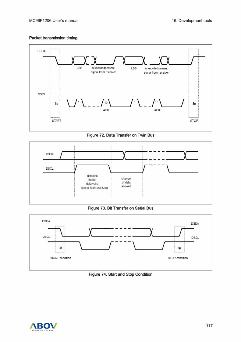
MC96F1206 User’s manual 16. Development tools
117
Packet transmission timing
Figure 72. Data Transfer on Twin Bus
Figure 73. Bit Transfer on Serial Bus
Figure 74. Start and Stop Condition

16. Development tools MC96F1206 User’s manual
118
Figure 75. Acknowledge on Serial Bus
Figure 76. Clock Synchronization during Wait Procedure

MC96F1206 User’s manual 16. Development tools
119
16.5.3 Connection of transmission
Two-pin interface connection uses open-drain (wire-AND bidirectional I/O).
Figure 77. Connection of Transmission
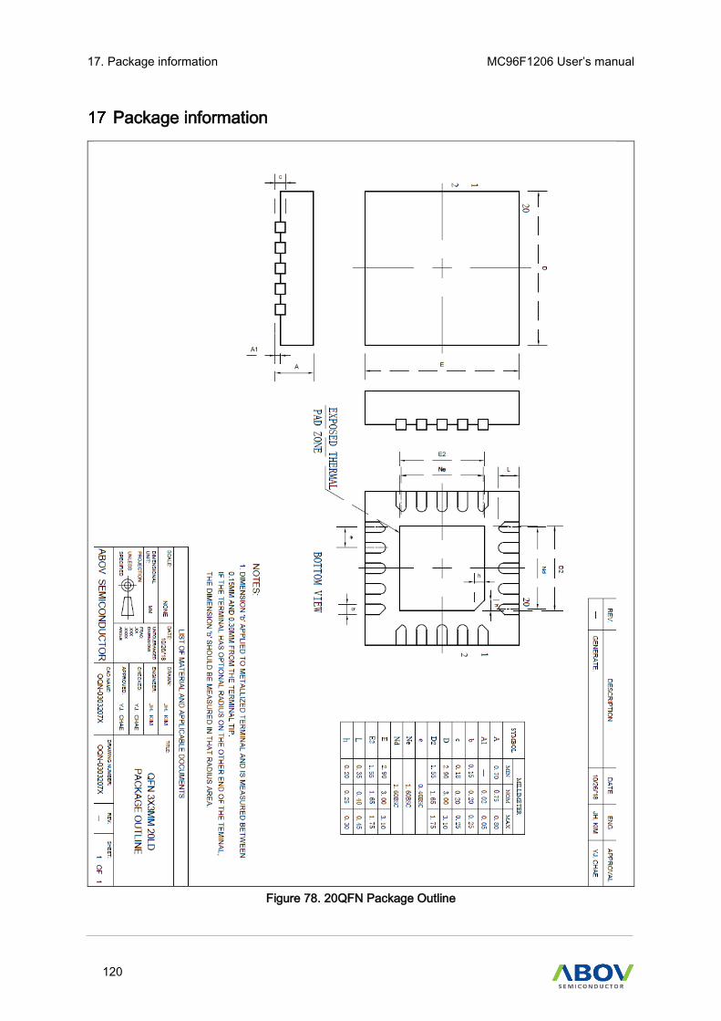
17. Package information MC96F1206 User’s manual
120
Package information
Figure 78. 20QFN Package Outline

MC96F1206 User’s manual 17. Package information
121
Figure 79. 20 TSSOP Package Outline

17. Package information MC96F1206 User’s manual
122
Figure 80. 16SOPN Package Outline

MC96F1206 User’s manual 18. Ordering information
123
Ordering information
Table 37. MC96F1206 Device Ordering Information
Device Name FLASH IRAM XRAM ADC I/O PORT Package
MC96F1206USBN 6 Kbytes 256 bytes - 15 inputs 18 20-QFN
MC96F1206RBN 6 Kbytes 256 bytes - 15 inputs 18 20-TSSOP
MC96F1206MBN 6 Kbytes 256 bytes - 12 inputs 14 16-SOPN
NOTE For more information on any aspect of this device, please contact your nearest distributor or ABOV sales
office.
Figure 81. MC96F1206 Device Numbering Nomenclature
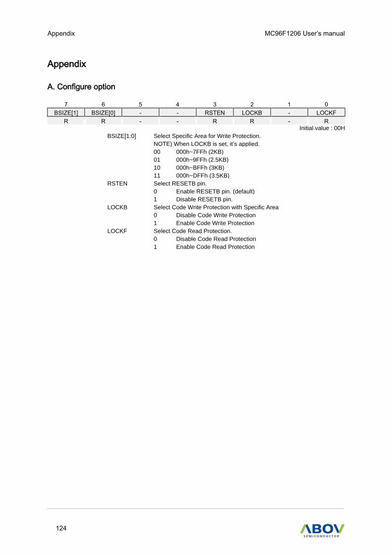
Appendix MC96F1206 User’s manual
124
Appendix
A. Configure option
7 6 5 4 3 2 1 0
BSIZE[1] BSIZE[0] - - RSTEN LOCKB - LOCKF
R R - - R R - R Initial value : 00H
BSIZE[1:0] Select Specific Area for Write Protection.
NOTE) When LOCKB is set, it’s applied.
00 000h~7FFh (2KB)
01 000h~9FFh (2.5KB)
10 000h~BFFh (3KB)
11 000h~DFFh (3.5KB)
RSTEN Select RESETB pin.
0 Enable RESETB pin. (default)
1 Disable RESETB pin.
LOCKB Select Code Write Protection with Specific Area
0 Disable Code Write Protection
1 Enable Code Write Protection
LOCKF Select Code Read Protection.
0 Disable Code Read Protection
1 Enable Code Read Protection

MC96F1206 User’s manual Appendix
125
B. Instruction table
• Instructions are either 1, 2 or 3 bytes long as listed in the ‘Bytes’ column in tables shown below.
• Each instruction takes either 1, 2 or 4 machine cycles to execute as listed in the following
tables in this section.
• 1 machine cycle comprises 2 system clock cycles.
Table 38. Instruction Table: Arithmetic
Arithmetic
Mnemonic Description Bytes Cycles Hex code
ADD A,Rn Add register to A 1 1 28-2F
ADD A,dir Add direct byte to A 2 1 25
ADD A,@Ri Add indirect memory to A 1 1 26-27
ADD A,#data Add immediate to A 2 1 24
ADDC A,Rn Add register to A with carry 1 1 38-3F
ADDC A,dir Add direct byte to A with carry 2 1 35
ADDC A,@Ri Add indirect memory to A with carry 1 1 36-37
ADDC A,#data Add immediate to A with carry 2 1 34
SUBB A,Rn Subtract register from A with borrow 1 1 98-9F
SUBB A,dir Subtract direct byte from A with borrow 2 1 95
SUBB A,@Ri Subtract indirect memory from A with borrow 1 1 96-97
SUBB A,#data Subtract immediate from A with borrow 2 1 94
INC A Increment A 1 1 04
INC Rn Increment register 1 1 08-0F
INC dir Increment direct byte 2 1 05
INC @Ri Increment indirect memory 1 1 06-07
DEC A Decrement A 1 1 14
DEC Rn Decrement register 1 1 18-1F
DEC dir Decrement direct byte 2 1 15
DEC @Ri Decrement indirect memory 1 1 16-17
INC DPTR Increment data pointer 1 2 A3
MUL AB Multiply A by B 1 4 A4
DIV AB Divide A by B 1 4 84
DA A Decimal Adjust A 1 1 D4
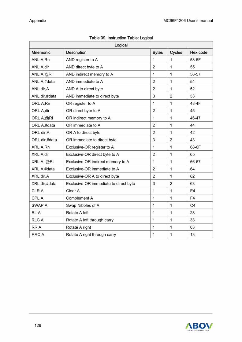
Appendix MC96F1206 User’s manual
126
Table 39. Instruction Table: Logical
Logical
Mnemonic Description Bytes Cycles Hex code
ANL A,Rn AND register to A 1 1 58-5F
ANL A,dir AND direct byte to A 2 1 55
ANL A,@Ri AND indirect memory to A 1 1 56-57
ANL A,#data AND immediate to A 2 1 54
ANL dir,A AND A to direct byte 2 1 52
ANL dir,#data AND immediate to direct byte 3 2 53
ORL A,Rn OR register to A 1 1 48-4F
ORL A,dir OR direct byte to A 2 1 45
ORL A,@Ri OR indirect memory to A 1 1 46-47
ORL A,#data OR immediate to A 2 1 44
ORL dir,A OR A to direct byte 2 1 42
ORL dir,#data OR immediate to direct byte 3 2 43
XRL A,Rn Exclusive-OR register to A 1 1 68-6F
XRL A,dir Exclusive-OR direct byte to A 2 1 65
XRL A, @Ri Exclusive-OR indirect memory to A 1 1 66-67
XRL A,#data Exclusive-OR immediate to A 2 1 64
XRL dir,A Exclusive-OR A to direct byte 2 1 62
XRL dir,#data Exclusive-OR immediate to direct byte 3 2 63
CLR A Clear A 1 1 E4
CPL A Complement A 1 1 F4
SWAP A Swap Nibbles of A 1 1 C4
RL A Rotate A left 1 1 23
RLC A Rotate A left through carry 1 1 33
RR A Rotate A right 1 1 03
RRC A Rotate A right through carry 1 1 13
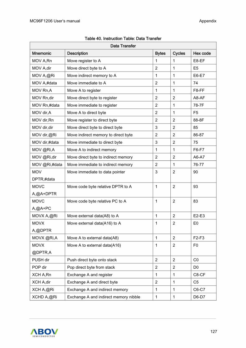
MC96F1206 User’s manual Appendix
127
Table 40. Instruction Table: Data Transfer
Data Transfer
Mnemonic Description Bytes Cycles Hex code
MOV A,Rn Move register to A 1 1 E8-EF
MOV A,dir Move direct byte to A 2 1 E5
MOV A,@Ri Move indirect memory to A 1 1 E6-E7
MOV A,#data Move immediate to A 2 1 74
MOV Rn,A Move A to register 1 1 F8-FF
MOV Rn,dir Move direct byte to register 2 2 A8-AF
MOV Rn,#data Move immediate to register 2 1 78-7F
MOV dir,A Move A to direct byte 2 1 F5
MOV dir,Rn Move register to direct byte 2 2 88-8F
MOV dir,dir Move direct byte to direct byte 3 2 85
MOV dir,@Ri Move indirect memory to direct byte 2 2 86-87
MOV dir,#data Move immediate to direct byte 3 2 75
MOV @Ri,A Move A to indirect memory 1 1 F6-F7
MOV @Ri,dir Move direct byte to indirect memory 2 2 A6-A7
MOV @Ri,#data Move immediate to indirect memory 2 1 76-77
MOV
DPTR,#data
Move immediate to data pointer 3 2 90
MOVC
A,@A+DPTR
Move code byte relative DPTR to A 1 2 93
MOVC
A,@A+PC
Move code byte relative PC to A 1 2 83
MOVX A,@Ri Move external data(A8) to A 1 2 E2-E3
MOVX
A,@DPTR
Move external data(A16) to A 1 2 E0
MOVX @Ri,A Move A to external data(A8) 1 2 F2-F3
MOVX
@DPTR,A
Move A to external data(A16) 1 2 F0
PUSH dir Push direct byte onto stack 2 2 C0
POP dir Pop direct byte from stack 2 2 D0
XCH A,Rn Exchange A and register 1 1 C8-CF
XCH A,dir Exchange A and direct byte 2 1 C5
XCH A,@Ri Exchange A and indirect memory 1 1 C6-C7
XCHD A,@Ri Exchange A and indirect memory nibble 1 1 D6-D7
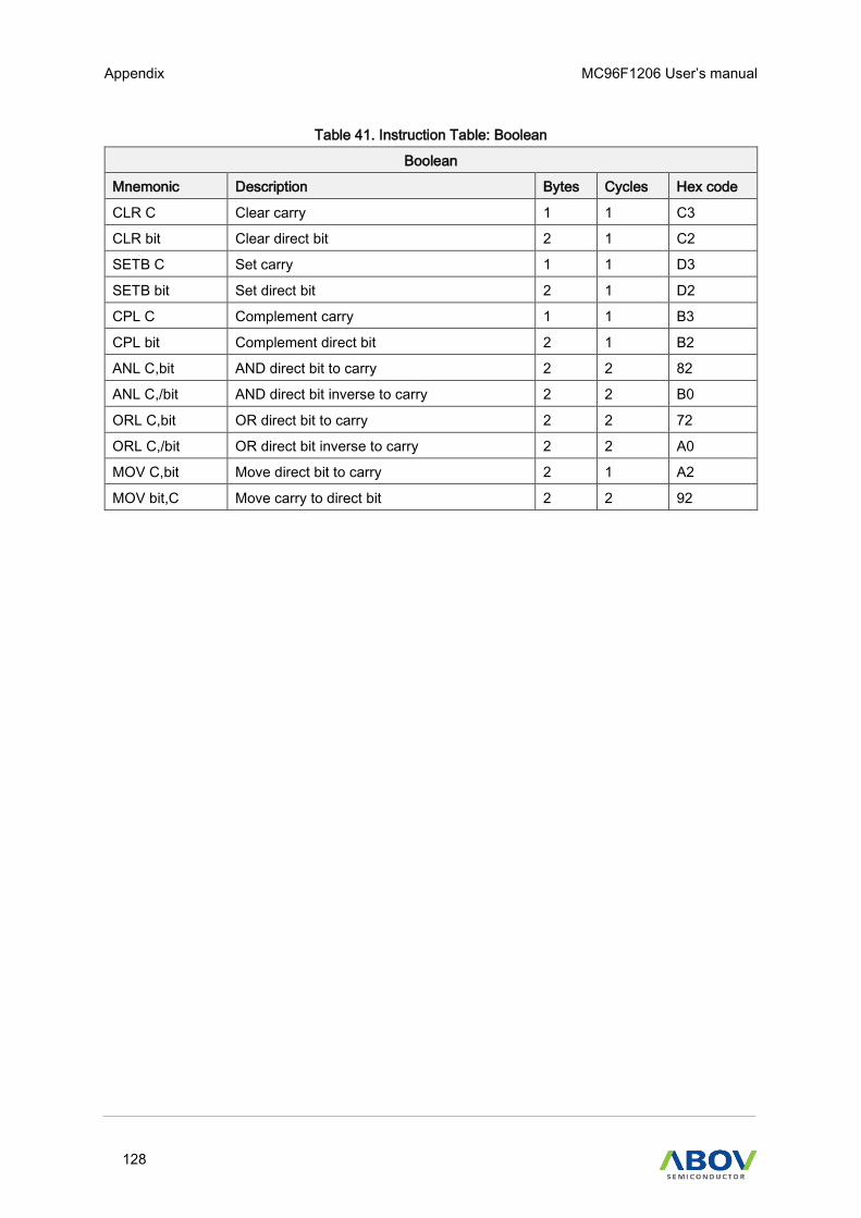
Appendix MC96F1206 User’s manual
128
Table 41. Instruction Table: Boolean
Boolean
Mnemonic Description Bytes Cycles Hex code
CLR C Clear carry 1 1 C3
CLR bit Clear direct bit 2 1 C2
SETB C Set carry 1 1 D3
SETB bit Set direct bit 2 1 D2
CPL C Complement carry 1 1 B3
CPL bit Complement direct bit 2 1 B2
ANL C,bit AND direct bit to carry 2 2 82
ANL C,/bit AND direct bit inverse to carry 2 2 B0
ORL C,bit OR direct bit to carry 2 2 72
ORL C,/bit OR direct bit inverse to carry 2 2 A0
MOV C,bit Move direct bit to carry 2 1 A2
MOV bit,C Move carry to direct bit 2 2 92

MC96F1206 User’s manual Appendix
129
Table 42. Instruction Table: Branching
Branching
Mnemonic Description Bytes Cycles Hex code
ACALL addr 11 Absolute jump to subroutine 2 2 11→F1
LCALL addr 16 Long jump to subroutine 3 2 12
RET Return from subroutine 1 2 22
RETI Return from interrupt 1 2 32
AJMP addr 11 Absolute jump unconditional 2 2 01→E1
LJMP addr 16 Long jump unconditional 3 2 02
SJMP rel Short jump (relative address) 2 2 80
JC rel Jump on carry = 1 2 2 40
JNC rel Jump on carry = 0 2 2 50
JB bit,rel Jump on direct bit = 1 3 2 20
JNB bit,rel Jump on direct bit = 0 3 2 30
JBC bit,rel Jump on direct bit = 1 and clear 3 2 10
JMP @A+DPTR Jump indirect relative DPTR 1 2 73
JZ rel Jump on accumulator = 0 2 2 60
JNZ rel Jump on accumulator ≠0 2 2 70
CJNE A,dir,rel Compare A,direct jne relative 3 2 B5
CJNE A,#d,rel Compare A,immediate jne relative 3 2 B4
CJNE Rn,#d,rel Compare register, immediate jne relative 3 2 B8-BF
CJNE
@Ri,#d,rel
Compare indirect, immediate jne relative 3 2 B6-B7
DJNZ Rn,rel Decrement register, jnz relative 2 2 D8-DF
DJNZ dir,rel Decrement direct byte, jnz relative 3 2 D5
Table 43. Instruction Table: Miscellaneous
Miscellaneous
Mnemonic Description Bytes Cycles Hex code
NOP No operation 1 1 00

Appendix MC96F1206 User’s manual
130
Table 44. Instruction Table: Additional Instructions
Additional instructions (selected through EO[7:4])
Mnemonic Description Bytes Cycles Hex code
MOVC
@(DPTR++),A
M8051W/M8051EW-specific instruction
supporting software download into program
memory
1 2 A5
TRAP Software break command 1 1 A5
In the above table, an entry such as E8-EF indicates a continuous block of hex opcodes used for 8
different registers, and the register numbers of which are defined by the lowest three bits of the
corresponding code. Non-continuous blocks of codes, shown as 11→F1 (for example), are used for
absolute jumps and calls, with the top 3 bits of the code being used to store the top three bits of the
destination address.
The CJNE instructions use the abbreviation #d for immediate data; other instructions use #data.

MC96F1206 User’s manual Appendix
131
C. Flash protection for invalid erase/ write
Appendix C shows example code to prevent code or data from being changed by abnormal operations
such as noise, unstable power, and malfunction.
Figure 82. Flash Protection against Abnormal Operations
How to protect the flash
• Divide into decision and execution to Erase/Write in flash.
− Check the program sequence from decision to execution in order of precedence about
Erase/Write.
− Setting the flags in program and check the flags in main loop at the end
− When the Flash Erase/Write is executed, check the flags. If not matched, do not execute.
• Check the range of Flash Sector Address
− If the flash sector address is outside of specific area, do not execute.
• Use the Dummy Address
− Set the flash sector address to dummy address in usually run time.
− Change the flash sector address to real area range shortly before Erase/Write.
− Even if invalid Erase/Write occurred, it will be Erase/Write in dummy address in flash.
• Use the LVR/LVI
− Unstable or low powers give an adverse effect on MCU. So use the LVR/LVI

Appendix MC96F1206 User’s manual
132
Protection flow description
The flash protection procedure is described in flowchart in figure 129, and each step in the figure 129
is introduced in the following lists:
1. Initialization
− Set the LVR/LVI. Check the power by LVR/LVI and do not execute under unstable or low
power.
− Initialize User_ID1/2/3
− Set Flash Sector Address High/Middle/Low to Dummy address. Dummy address is set to
unused area range in flash.
2. Decide to Write
− When the Erase/Write are determined, set flag. Do not directly Erase/Write in flash.
− Make the user data.
3. Check and Set User_ID1/2/3
− In the middle of source, insert code which can check and set the flags.
− By setting the User_ID 1/2/3 sequentially and identify the flow of the program.
4. Set Flash Sector Address
− Set address to real area range shortly before Erase/Write in flash.
− Set to Dummy address after Erase/Write. Even if invalid work occurred, it will be
Erase/Write in Dummy address in flash.
5. Check Flags
— If every flag (User_ID1/2/3, LVI, Flash Address Min/Max) was set, than do Erase/Write.
— If the Flash Sector Address is outside of Min/Max, do not execute
— Address Min/Max is set to unused area.
6. Initialize Flags
— Initialize User_ID1/2/3
— Set Flash Sector Address to Dummy Address
Sample Source
— Refer to the ABOV website (www.abovsemi.com).
— It is created based on the MC97F2664.
— Each product should be modified according to the Page Buffer Size and Flash Size

MC96F1206 User’s manual Appendix
133
InitialSet LVR/LVI more than 2.0V
Start Main Loop
Working
Start
Write Flash? Set User_ID1
Working
Check User_ID1? Set User_ID2
Working
Check User_ID2? Set User_ID3
Working
Yes
Yes
Yes
No
No
No
Write Flash
Clear User_ID1/2/3Clear FEMRClear FECRSet FEALH/M/L to Dummy Addr
Check User_ID1/2/3
Set FEALH/M/LSet FEMR
Sef FECRCheck LVIYes Yes
No No
Check Flash Addr Min/Max
No
Yes
d
①
② ③
③
③
④
⑤
⑥
⑤ ⑤
Figure 83. Flowchart of Flash Protection

Appendix MC96F1206 User’s manual
134
Other protection by the configure options
Protection by Configure option
— Set flash protection by MCU Write Tool (OCD, PGM+, etc.)
Vector Area:
00H~FFH
Specific Area:
2KBytes (Address 000H – 07FFH)
2.5KBytes (Address 0000H – 09FFH)
3KBytes (Address 0000H – 0BFFH)
3.5KBytes (Address 0000H – 0DFFH)
— The range of protection may be different each product.

MC96F1206 User’s manual Important notice
135
Revision history
Date Revision Description
2019-09-05 1.00 First creation
2020-03-20 1.10 Renewal
2020-07-01 1.20 Changed the body information of 20 QFN package from 4x4 mm to
3x3 mm.
2020-07-20 1.21 Corrected Internal RC oscillator to 32MHz at Table 1. MC96F1206
Device Features and Peripheral Counts.
Corrected the values for block diagram at Figure 2. MC96F1206
Block Diagram.

Important notice A31G32x Datasheet
136
ABOV Disclaimer IMPORTANT NOTICE – PLEASE READ CAREFULLY
ABOV Semiconductor ("ABOV") reserves the right to make changes, corrections, enhancements, modifications, and improvements to ABOV products and/or to this document at any time without notice. ABOV does not give warranties as to the accuracy or completeness of the information included herein. Purchasers should obtain the latest relevant information of ABOV products before placing orders. Purchasers are entirely responsible for the choice, selection, and use of ABOV products and ABOV assumes no liability for application assistance or the design of purchasers’ products. No license, express or implied, to any intellectual property rights is granted by ABOV herein. ABOV disclaims all express and implied warranties and shall not be responsible or liable for any injuries or damages related to use of ABOV products in such unauthorized applications. ABOV and the ABOV logo are trademarks of ABOV. All other product or service names are the property of their respective owners. Information in this document supersedes and replaces the information previously supplied in any former versions of this document.
© 2020 ABOV Semiconductor – All rights reserved
Korea
Regional Office, Seoul HQ, Ochang
R&D, Marketing & Sales R&D, QA, and Test Center
8th Fl., 330, Yeongdong-daero, Gangnam-gu, Seoul, 06177, Korea
93, Gangni 1-gil, Ochang-eup, Cheongwon-gun, Chungcheongbuk-do, 28126, Korea
Tel: +82-2-2193-2200 Fax: +82-2-508-6903 www.abovsemi.com
Tel: +82-43-219-5200 Fax: +82-43-217-3534 www.abovsemi.com
Domestic Sales Manager Global Sales Manager China Sales Manager Tel: +82-2-2193-2206 Fax: +82-2-508-6903 Email: [email protected]
Tel: +82-2-2193-2281 Fax: +82-2-508-6903 Email: [email protected]
Tel: +86-755-8287-2205 Fax: +86-755-8287-2204 Email: [email protected]