mcf51ac256 series coldfire microcontroller - data...
TRANSCRIPT
Freescale SemiconductorData Sheet: Technical Data
Document Number: MCF51AC256Rev.7, 9/2011
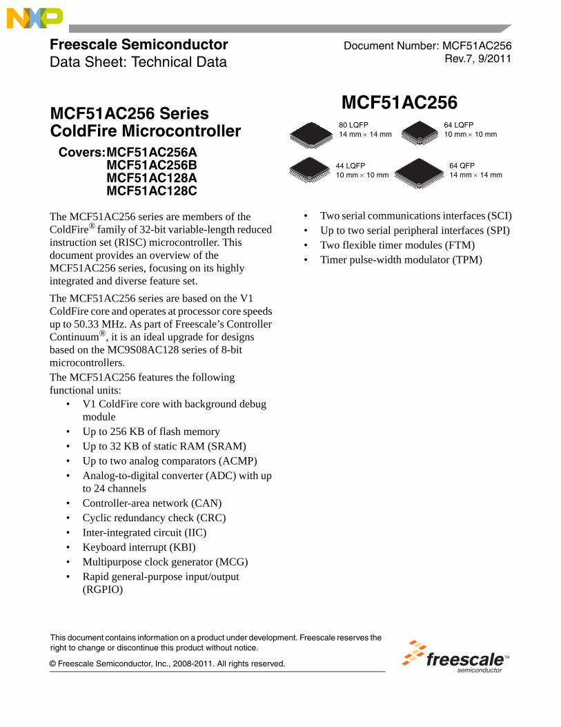
MCF51AC25680 LQFP14 mm 14 mm
64 LQFP10 mm 10 mm
64 QFP14 mm 14 mm
44 LQFP10 mm 10 mm
MCF51AC256 Series ColdFire Microcontroller
Covers:MCF51AC256AMCF51AC256BMCF51AC128AMCF51AC128C
The MCF51AC256 series are members of the ColdFire® family of 32-bit variable-length reduced instruction set (RISC) microcontroller. This document provides an overview of the MCF51AC256 series, focusing on its highly integrated and diverse feature set.
The MCF51AC256 series are based on the V1 ColdFire core and operates at processor core speeds up to 50.33 MHz. As part of Freescale’s Controller Continuum®, it is an ideal upgrade for designs based on the MC9S08AC128 series of 8-bit microcontrollers.The MCF51AC256 features the following functional units:
• V1 ColdFire core with background debug module
• Up to 256 KB of flash memory• Up to 32 KB of static RAM (SRAM)• Up to two analog comparators (ACMP)• Analog-to-digital converter (ADC) with up
to 24 channels• Controller-area network (CAN) • Cyclic redundancy check (CRC) • Inter-integrated circuit (IIC) • Keyboard interrupt (KBI) • Multipurpose clock generator (MCG)• Rapid general-purpose input/output
(RGPIO)
© Freescale Semiconductor, Inc., 2008-2011. All rights reserved
This document contains information on a product under developmright to change or discontinue this product without notice.
• Two serial communications interfaces (SCI)• Up to two serial peripheral interfaces (SPI)• Two flexible timer modules (FTM)• Timer pulse-width modulator (TPM)
.
ent. Freescale reserves the

MCF51AC256 ColdFire Microcontroller Data Sheet, Rev.7
Freescale Semiconductor2
Table of Contents1 MCF51AC256 Family Configurations . . . . . . . . . . . . . . . . . . . .3
1.1 Device Comparison. . . . . . . . . . . . . . . . . . . . . . . . . . . . .31.2 Block Diagram. . . . . . . . . . . . . . . . . . . . . . . . . . . . . . . . .41.3 Features . . . . . . . . . . . . . . . . . . . . . . . . . . . . . . . . . . . . .6
1.3.1 Feature List . . . . . . . . . . . . . . . . . . . . . . . . . . . . .71.4 Part Numbers . . . . . . . . . . . . . . . . . . . . . . . . . . . . . . . .101.5 Pinouts and Packaging . . . . . . . . . . . . . . . . . . . . . . . . .12
2 Electrical Characteristics . . . . . . . . . . . . . . . . . . . . . . . . . . . .172.1 Parameter Classification . . . . . . . . . . . . . . . . . . . . . . . .172.2 Absolute Maximum Ratings . . . . . . . . . . . . . . . . . . . . .172.3 Thermal Characteristics . . . . . . . . . . . . . . . . . . . . . . . .182.4 Electrostatic Discharge (ESD) Protection Characteristics
192.5 DC Characteristics . . . . . . . . . . . . . . . . . . . . . . . . . . . .202.6 Supply Current Characteristics . . . . . . . . . . . . . . . . . . .252.7 Analog Comparator (ACMP) Electricals . . . . . . . . . . . .272.8 ADC Characteristics . . . . . . . . . . . . . . . . . . . . . . . . . . .282.9 External Oscillator (XOSC) Characteristics . . . . . . . . .312.10 MCG Specifications . . . . . . . . . . . . . . . . . . . . . . . . . . .322.11 AC Characteristics . . . . . . . . . . . . . . . . . . . . . . . . . . . .33
2.11.1 Control Timing . . . . . . . . . . . . . . . . . . . . . . . . . .342.11.2 Timer (TPM/FTM) Module Timing . . . . . . . . . . .352.11.3 MSCAN . . . . . . . . . . . . . . . . . . . . . . . . . . . . . . .35
2.12 SPI Characteristics . . . . . . . . . . . . . . . . . . . . . . . . . . . .362.13 Flash Specifications . . . . . . . . . . . . . . . . . . . . . . . . . . .382.14 EMC Performance. . . . . . . . . . . . . . . . . . . . . . . . . . . . .39
2.14.1 Radiated Emissions. . . . . . . . . . . . . . . . . . . . . .393 Mechanical Outline Drawings . . . . . . . . . . . . . . . . . . . . . . . . .404 Revision History . . . . . . . . . . . . . . . . . . . . . . . . . . . . . . . . . . .41
List of FiguresFigure 1.MCF51AC256 Series Block Diagram . . . . . . . . . . . . . . 5Figure 2.MCF51AC256 Series ColdFire Microcontroller
80-Pin LQFP . . . . . . . . . . . . . . . . . . . . . . . . . . . . . . . . 12Figure 3.MCF51AC256 Series ColdFire Microcontroller
64-Pin QFP/LQFP. . . . . . . . . . . . . . . . . . . . . . . . . . . . 13Figure 4.MCF51AC256 Series ColdFire Microcontroller
44-Pin LQFP . . . . . . . . . . . . . . . . . . . . . . . . . . . . . . . . 14Figure 5.Typical IOH vs. VDD–VOH at VDD = 3 V
(Low Drive, PTxDSn = 0) . . . . . . . . . . . . . . . . . . . . . . 22Figure 6.Typical IOH vs. VDD–VOH at VDD = 3 V
(High Drive, PTxDSn = 1) . . . . . . . . . . . . . . . . . . . . . . 23Figure 7.Typical IOH vs. VDD–VOH at VDD = 5 V
(Low Drive, PTxDSn = 0) . . . . . . . . . . . . . . . . . . . . . . 23
Figure 8.Typical IOH vs. VDD–VOH at VDD = 5 V (High Drive, PTxDSn = 1) . . . . . . . . . . . . . . . . . . . . . . 24
Figure 9.Typical Run IDD vs. System Clock Freq. for FEI and FBE Modes . . . . . . . . . . . . . . . . . . . . . . . . 27
Figure 10.ADC Input Impedance Equivalency Diagram. . . . . . . 29Figure 11.Reset Timing . . . . . . . . . . . . . . . . . . . . . . . . . . . . . . . 34Figure 12.IRQ/KBIPx Timing . . . . . . . . . . . . . . . . . . . . . . . . . . . 34Figure 13.Timer External Clock . . . . . . . . . . . . . . . . . . . . . . . . . 35Figure 14.Timer Input Capture Pulse . . . . . . . . . . . . . . . . . . . . . 35Figure 15.SPI Master Timing (CPHA = 0) . . . . . . . . . . . . . . . . . 37Figure 16.SPI Master Timing (CPHA =1) . . . . . . . . . . . . . . . . . . 37Figure 17.SPI Slave Timing (CPHA = 0) . . . . . . . . . . . . . . . . . . 38Figure 18.SPI Slave Timing (CPHA = 1) . . . . . . . . . . . . . . . . . . 38
List of TablesTable 1. MCF51AC256 Series Device Comparison . . . . . . . . . . 3Table 2. MCF51AC256 Series Functional Units . . . . . . . . . . . . . 6Table 3. Orderable Part Number Summary. . . . . . . . . . . . . . . . 10Table 4. Pin Availability by Package Pin-Count . . . . . . . . . . . . . 14Table 5. Parameter Classifications . . . . . . . . . . . . . . . . . . . . . . 17Table 6. Absolute Maximum Ratings. . . . . . . . . . . . . . . . . . . . . 18Table 7. Thermal Characteristics. . . . . . . . . . . . . . . . . . . . . . . . 18Table 8. ESD and Latch-up Test Conditions . . . . . . . . . . . . . . . 20Table 9. ESD and Latch-Up Protection Characteristics. . . . . . . 20Table 10.DC Characteristics. . . . . . . . . . . . . . . . . . . . . . . . . . . . 20Table 11. Supply Current Characteristics. . . . . . . . . . . . . . . . . . 25Table 12.Analog Comparator Electrical Specifications. . . . . . . . 27Table 13.5 Volt 12-bit ADC Operating Conditions . . . . . . . . . . . 28Table 14.5 Volt 12-bit ADC Characteristics
(VREFH = VDDA, VREFL = VSSA) . . . . . . . . . . . . . . . . . . 29Table 15.Oscillator Electrical Specifications
(Temperature Range = –40 to 105 C Ambient) . . . . . 31Table 16.MCG Frequency Specifications
(Temperature Range = –40 to 105 C Ambient) . . . . . 32Table 17.Control Timing . . . . . . . . . . . . . . . . . . . . . . . . . . . . . . . 34Table 18.TPM/FTM Input Timing . . . . . . . . . . . . . . . . . . . . . . . . 35Table 19.MSCAN Wake-Up Pulse Characteristics . . . . . . . . . . . 35Table 20.SPI Timing . . . . . . . . . . . . . . . . . . . . . . . . . . . . . . . . . . 36Table 21.Flash Characteristics . . . . . . . . . . . . . . . . . . . . . . . . . . 39Table 22.Package Information . . . . . . . . . . . . . . . . . . . . . . . . . . 40Table 23.Revision History. . . . . . . . . . . . . . . . . . . . . . . . . . . . . . 41
MCF51AC256 Family Configurations
F
R
Vd
A
A
A(
C
C
C
R
D
II
IR
IN
K
L
M
O
P
R
Sin
S
S
F
F
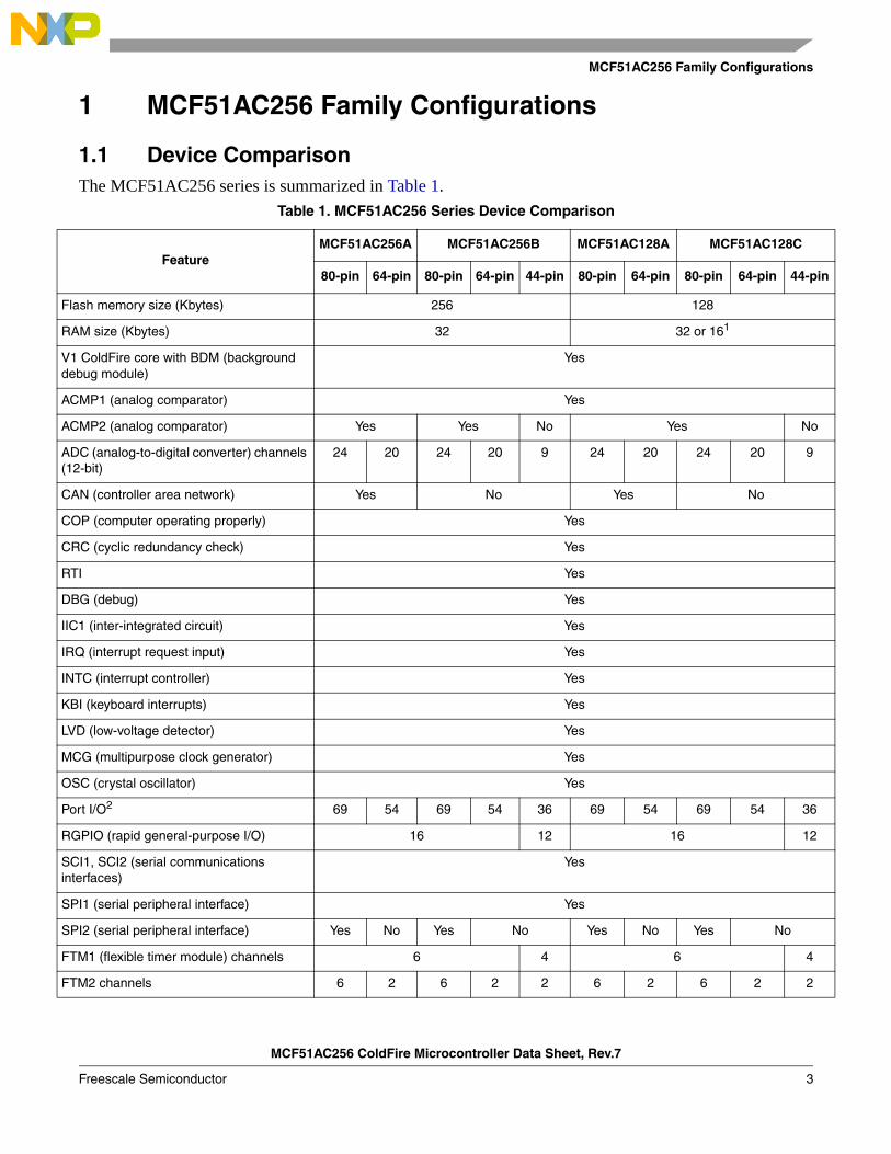
1 MCF51AC256 Family Configurations
1.1 Device ComparisonThe MCF51AC256 series is summarized in Table 1.
Table 1. MCF51AC256 Series Device Comparison
FeatureMCF51AC256A MCF51AC256B MCF51AC128A MCF51AC128C
80-pin 64-pin 80-pin 64-pin 44-pin 80-pin 64-pin 80-pin 64-pin 44-pin
lash memory size (Kbytes) 256 128
AM size (Kbytes) 32 32 or 161
1 ColdFire core with BDM (background ebug module)
Yes
CMP1 (analog comparator) Yes
CMP2 (analog comparator) Yes Yes No Yes No
DC (analog-to-digital converter) channels 12-bit)
24 20 24 20 9 24 20 24 20 9
AN (controller area network) Yes No Yes No
OP (computer operating properly) Yes
RC (cyclic redundancy check) Yes
TI Yes
BG (debug) Yes
C1 (inter-integrated circuit) Yes
Q (interrupt request input) Yes
TC (interrupt controller) Yes
BI (keyboard interrupts) Yes
VD (low-voltage detector) Yes
CG (multipurpose clock generator) Yes
SC (crystal oscillator) Yes
ort I/O2 69 54 69 54 36 69 54 69 54 36
GPIO (rapid general-purpose I/O) 16 12 16 12
CI1, SCI2 (serial communications terfaces)
Yes
PI1 (serial peripheral interface) Yes
PI2 (serial peripheral interface) Yes No Yes No Yes No Yes No
TM1 (flexible timer module) channels 6 4 6 4
TM2 channels 6 2 6 2 2 6 2 6 2 2
MCF51AC256 ColdFire Microcontroller Data Sheet, Rev.7
Freescale Semiconductor 3

MCF51AC256 Family Configurations
Tc
V
1
2
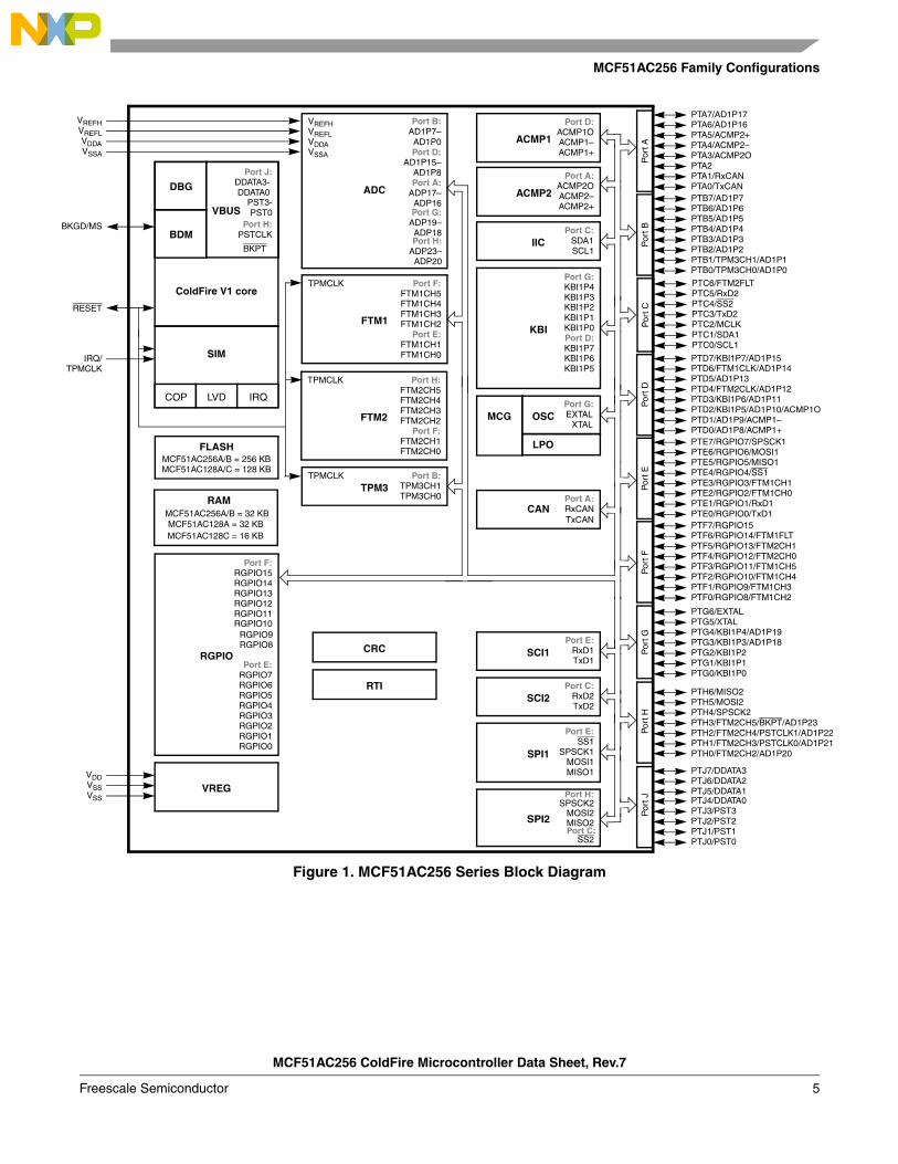
1.2 Block DiagramFigure 1 shows the connections between the MCF51AC256 series pins and modules.
PM3 (timer pulse-width modulator) hannels
2
BUS (debug visibility bus) Yes No Yes No Yes No Yes No
The members of MCF51AC128A with CAN support have 32 KB RAM. The other members have 16 KB RAM.
Up to 16 pins on Ports E and F are shared with the ColdFire Rapid GPIO module.
Table 1. MCF51AC256 Series Device Comparison (continued)
FeatureMCF51AC256A MCF51AC256B MCF51AC128A MCF51AC128C
80-pin 64-pin 80-pin 64-pin 44-pin 80-pin 64-pin 80-pin 64-pin 44-pin
MCF51AC256 ColdFire Microcontroller Data Sheet, Rev.7
Freescale Semiconductor4
MCF51AC256 Family Configurations
B
Figure 1. MCF51AC256 Series Block Diagram
Por
t B
PTB3/AD1P3PTB4/AD1P4PTB5/AD1P5
PTB2/AD1P2PTB1/TPM3CH1/AD1P1PTB0/TPM3CH0/AD1P0
PTB6/AD1P6PTB7/AD1P7
Por
t D
PTD3/KBI1P6/AD1P11PTD4/FTM2CLK/AD1P12PTD5/AD1P13
PTD2/KBI1P5/AD1P10/ACMP1OPTD1/AD1P9/ACMP1–PTD0/AD1P8/ACMP1+
PTD6/FTM1CLK/AD1P14PTD7/KBI1P7/AD1P15
Por
t C PTC3/TxD2PTC4/SS2PTC5/RxD2
PTC2/MCLKPTC1/SDA1PTC0/SCL1
PTC6/FTM2FLT
Por
t F
PTF3/RGPIO11/FTM1CH5PTF4/RGPIO12/FTM2CH0PTF5/RGPIO13/FTM2CH1
PTF2/RGPIO10/FTM1CH4PTF1/RGPIO9/FTM1CH3PTF0/RGPIO8/FTM1CH2
PTF6/RGPIO14/FTM1FLTPTF7/RGPIO15
Por
t E
PTE3/RGPIO3/FTM1CH1PTE4/RGPIO4/SS1PTE5/RGPIO5/MISO1
PTE2/RGPIO2/FTM1CH0PTE1/RGPIO1/RxD1PTE0/RGPIO0/TxD1
PTE6/RGPIO6/MOSI1PTE7/RGPIO7/SPSCK1
Por
t G PTG3/KBI1P3/AD1P18PTG4/KBI1P4/AD1P19PTG5/XTAL
PTG2/KBI1P2PTG1/KBI1P1PTG0/KBI1P0
PTG6/EXTAL
Por
t H
PTH3/FTM2CH5/BKPT/AD1P23PTH4/SPSCK2
PTH2/FTM2CH4/PSTCLK1/AD1P22PTH1/FTM2CH3/PSTCLK0/AD1P21PTH0/FTM2CH2/AD1P20
Por
t J
PTJ3/PST3PTJ4/DDATA0
PTJ2/PST2PTJ1/PST1PTJ0/PST0
Por
t A
PTA3/ACMP2OPTA4/ACMP2–PTA5/ACMP2+
PTA2PTA1/RxCANPTA0/TxCAN
PTA6/AD1P16PTA7/AD1P17
ADC
VREFHVREFLVDDAVSSA
CAN
TPMCLK
FTM1
TPMCLK
SPI1
SCI1
MCG
VREG
SIM
ColdFire V1 core
Port G:EXTAL
XTAL
Port E:RxD1TxD1
Port E:SS1
SPSCK1MOSI1MISO1
Port F:FTM1CH5FTM1CH4FTM1CH3FTM1CH2
Port E:FTM1CH1FTM1CH0
TPM3Port B:
TPM3CH1TPM3CH0 Port A:
RxCANTxCAN
IICPort C:
SDA1SCL1
SCI2Port C:
RxD2TxD2
Port B:AD1P7–AD1P0Port D:
AD1P15–AD1P8
SPI2
Port H:SPSCK2
MOSI2MISO2
KBI
Port G:KBI1P4KBI1P3
KBI1P1
Port D:KBI1P7KBI1P6KBI1P5
KBI1P2
RGPIO
Port F:RGPIO15RGPIO14RGPIO13RGPIO12RGPIO11RGPIO10
RGPIO9RGPIO8
Port E:RGPIO7RGPIO6RGPIO5RGPIO4RGPIO3RGPIO2RGPIO1RGPIO0
ACMP1
Port D:ACMP1OACMP1–ACMP1+
RTI
IRQ/
VREFHVREFLVDDAVSSA
KGD/MS
RESET
VDDVSSVSS
COP
FLASHMCF51AC256A/B = 256 KB
OSC
DBG
FTM2
TPMCLK Port H:FTM2CH5FTM2CH4FTM2CH3FTM2CH2
Port F:FTM2CH1FTM2CH0
Port A:ADP17–
ADP16Port G:
ADP19–ADP18Port H:
ADP23–ADP20
ACMP2
Port A:ACMP2OACMP2–ACMP2+
PTH6/MISO2PTH5/MOSI2
PTJ7/DDATA3PTJ6/DDATA2PTJ5/DDATA1
TPMCLK
CRC
VBUS
Port J:DDATA3-DDATA0
PST0Port H:
PSTCLK
BKPT
PST3-
KBI1P0
MCF51AC128A/C = 128 KB
RAMMCF51AC256A/B = 32 KBMCF51AC128A = 32 KB
BDM
LVD IRQ
MCF51AC128C = 16 KB
Port C:SS2
LPO
MCF51AC256 ColdFire Microcontroller Data Sheet, Rev.7
Freescale Semiconductor 5
MCF51AC256 Family Configurations
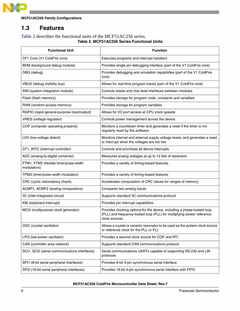
1.3 FeaturesTable 2 describes the functional units of the MCF51AC256 series.
Table 2. MCF51AC256 Series Functional Units
Functional Unit Function
CF1 Core (V1 ColdFire core) Executes programs and interrupt handlers
BDM (background debug module) Provides single pin debugging interface (part of the V1 ColdFire core)
DBG (debug) Provides debugging and emulation capabilities (part of the V1 ColdFire core)
VBUS (debug visibility bus) Allows for real-time program traces (part of the V1 ColdFire core)
SIM (system integration module) Controls resets and chip level interfaces between modules
Flash (flash memory) Provides storage for program code, constants and variables
RAM (random-access memory) Provides storage for program variables
RGPIO (rapid general-purpose input/output) Allows for I/O port access at CPU clock speeds
VREG (voltage regulator) Controls power management across the device
COP (computer operating properly) Monitors a countdown timer and generates a reset if the timer is not regularly reset by the software
LVD (low-voltage detect) Monitors internal and external supply voltage levels, and generates a reset or interrupt when the voltages are too low
CF1_INTC (interrupt controller) Controls and prioritizes all device interrupts
ADC (analog-to-digital converter) Measures analog voltages at up to 12 bits of resolution
FTM1, FTM2 (flexible timer/pulse-width modulators)
Provides a variety of timing-based features
TPM3 (timer/pulse-width modulator) Provides a variety of timing-based features
CRC (cyclic redundancy check) Accelerates computation of CRC values for ranges of memory
ACMP1, ACMP2 (analog comparators) Compares two analog inputs
IIC (inter-integrated circuit) Supports standard IIC communications protocol
KBI (keyboard interrupt) Provides pin interrupt capabilities
MCG (multipurpose clock generator) Provides clocking options for the device, including a phase-locked loop (PLL) and frequency-locked loop (FLL) for multiplying slower reference clock sources
OSC (crystal oscillator) Allows a crystal or ceramic resonator to be used as the system clock source or reference clock for the PLL or FLL
LPO (low-power oscillator) Provides a second clock source for COP and RTI.
CAN (controller area network) Supports standard CAN communications protocol
SCI1, SCI2 (serial communications interfaces) Serial communications UARTs capable of supporting RS-232 and LIN protocols
SPI1 (8-bit serial peripheral interfaces) Provides 8-bit 4-pin synchronous serial interface
SPI2 (16-bit serial peripheral interfaces) Provides 16-bit 4-pin synchronous serial interface with FIFO
MCF51AC256 ColdFire Microcontroller Data Sheet, Rev.7
Freescale Semiconductor6
MCF51AC256 Family Configurations
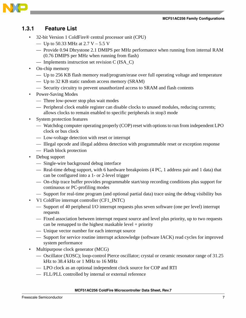
1.3.1 Feature List• 32-bit Version 1 ColdFire® central processor unit (CPU)
— Up to 50.33 MHz at 2.7 V – 5.5 V— Provide 0.94 Dhrystone 2.1 DMIPS per MHz performance when running from internal RAM
(0.76 DMIPS per MHz when running from flash)— Implements instruction set revision C (ISA_C)
• On-chip memory— Up to 256 KB flash memory read/program/erase over full operating voltage and temperature— Up to 32 KB static random access memory (SRAM)— Security circuitry to prevent unauthorized access to SRAM and flash contents
• Power-Saving Modes— Three low-power stop plus wait modes— Peripheral clock enable register can disable clocks to unused modules, reducing currents;
allows clocks to remain enabled to specific peripherals in stop3 mode• System protection features
— Watchdog computer operating properly (COP) reset with options to run from independent LPO clock or bus clock
— Low-voltage detection with reset or interrupt— Illegal opcode and illegal address detection with programmable reset or exception response— Flash block protection
• Debug support— Single-wire background debug interface— Real-time debug support, with 6 hardware breakpoints (4 PC, 1 address pair and 1 data) that
can be configured into a 1- or 2-level trigger — On-chip trace buffer provides programmable start/stop recording conditions plus support for
continuous or PC-profiling modes— Support for real-time program (and optional partial data) trace using the debug visibility bus
• V1 ColdFire interrupt controller (CF1_INTC)— Support of 40 peripheral I/O interrupt requests plus seven software (one per level) interrupt
requests— Fixed association between interrupt request source and level plus priority, up to two requests
can be remapped to the highest maskable level + priority— Unique vector number for each interrupt source— Support for service routine interrupt acknowledge (software IACK) read cycles for improved
system performance• Multipurpose clock generator (MCG)
— Oscillator (XOSC); loop-control Pierce oscillator; crystal or ceramic resonator range of 31.25 kHz to 38.4 kHz or 1 MHz to 16 MHz
— LPO clock as an optional independent clock source for COP and RTI— FLL/PLL controlled by internal or external reference
MCF51AC256 ColdFire Microcontroller Data Sheet, Rev.7
Freescale Semiconductor 7

MCF51AC256 Family Configurations
— Trimmable internal reference allows 0.2% resolution and 2% deviation• Analog-to-digital converter (ADC)
— 24 analog inputs with 12 bits resolution— Output formatted in 12-, 10- or 8-bit right-justified format— Single or continuous conversion (automatic return to idle after single conversion)— Operation in low-power modes for lower noise operation— Asynchronous clock source for lower noise operation— Automatic compare with interrupt for less-than, or greater-than or equal-to, programmable
value— On-chip temperature sensor
• Flexible timer/pulse-width modulators (FTM)— 16-bit Free-running counter or a counter with initial and final value. The counting can be up
and unsigned, up and signed, or up-down and unsigned— Up to 6 channels, and each channel can be configured for input capture, output compare or
edge-aligned PWM mode, all channels can be configured for center-aligned PWM mode– Channels can operate as pairs with equal outputs, pairs with complimentary outputs or
independent channels (with independent outputs)– Each pair of channels can be combined to generate a PWM signal (with independent control
of both edges of PWM signal)– Deadtime insertion is available for each complementary pair
— The load of the FTM registers which have write buffer can be synchronized; write protection for critical registers
— Generation of the triggers to ADC (hardware trigger)— A fault input for global fault control— Backwards compatible with TPM
• Timer/pulse width modulator (TPM)— 16-bit free-running or modulo up/down count operation— Two channels, each channel may be input capture, output compare, or edge-aligned PWM— One interrupt per channel plus terminal count interrupt
• Cyclic redundancy check (CRC) generator— High speed hardware CRC generator circuit using 16-bit shift register— CRC16-CCITT compliancy with x16 + x12 + x5 + 1 polynomial— Error detection for all single, double, odd, and most multi-bit errors— Programmable initial seed value
• Analog comparators (ACMP)— Full rail to rail supply operation— Selectable interrupt on rising edge, falling edge, or either rising or falling edges of comparator
output— Option to compare to fixed internal bandgap reference voltage— Option to allow comparator output to be visible on a pin, ACMPxO
MCF51AC256 ColdFire Microcontroller Data Sheet, Rev.7
Freescale Semiconductor8

MCF51AC256 Family Configurations
• Inter-integrated circuit (IIC)— Compatible with IIC bus standard— Multi-master operation— Software programmable for one of 64 different serial clock frequencies— Interrupt driven byte-by-byte data transfer— Arbitration lost interrupt with automatic mode switching from master to slave— Calling address identification interrupt— Bus busy detection— 10-bit address extension
• Controller area network (CAN)— Implementation of the CAN protocol — Version 2.0A/B
– Standard and extended data frames– Zero to eight bytes data length– Programmable bit rate up to 1 Mbps– Support for remote frames
— Five receive buffers with FIFO storage scheme— Three transmit buffers with internal prioritization using a “local priority” concept— Flexible maskable identifier filter supports two full-size (32-bit) extended identifier filters, four
16-bit filters, or eight 8-bit filters— Programmable wakeup functionality with integrated low-pass filter— Programmable loopback mode supports self-test operation— Programmable listen-only mode for monitoring of CAN bus— Programmable bus-off recovery functionality— Separate signalling and interrupt capabilities for all CAN receiver and transmitter error states
(warning, error passive, bus-off)— Internal timer for time-stamping of received and transmitted messages
• Serial communications interfaces (SCI)— Full-duplex, standard non-return-to-zero (NRZ) format— Double-buffered transmitter and receiver with separate enables— Programmable baud rates (13-bit modulo divider)— Interrupt-driven or polled operation— Hardware parity generation and checking— Programmable 8-bit or 9-bit character length— Receiver wakeup by idle-line or address-mark— Optional 13-bit break character generation / 11-bit break character detection— Selectable transmitter output polarity
• Serial peripheral interfaces (SPI)— Master or slave mode operation— Full-duplex or single-wire bidirectional option— Programmable transmit bit rate
MCF51AC256 ColdFire Microcontroller Data Sheet, Rev.7
Freescale Semiconductor 9

MCF51AC256 Family Configurations
— Double-buffered transmit and receive— Serial clock phase and polarity options— Slave select output— Selectable MSB-first or LSB-first shifting— 16-bit and FIFO operations in SPI2
• Input/Output— 69 GPIOs— 8 keyboard interrupt pins with selectable polarity— Hysteresis and configurable pull-up device on all input pins; Configurable slew rate and drive
strength on all output pins— 16-bits Rapid GPIO pins connected to the processor’s local 32-bit platform bus with set, clear,
and faster toggle functionality
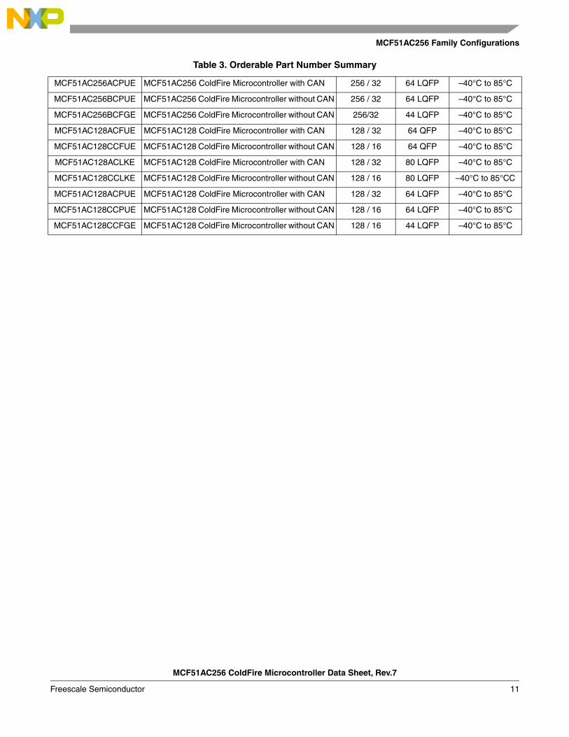
1.4 Part Numbers
Table 3. Orderable Part Number Summary
Freescale Part Number DescriptionFlash / SRAM
(Kbytes)Package Temperature
MCF51AC256AVFUE MCF51AC256 ColdFire Microcontroller with CAN 256 / 32 64 QFP –40°C to 105°C
MCF51AC256BVFUE MCF51AC256 ColdFire Microcontroller without CAN 256 / 32 64 QFP –40°C to 105°C
MCF51AC256AVLKE MCF51AC256 ColdFire Microcontroller with CAN 256 / 32 80 LQFP –40°C to 105°C
MCF51AC256BVLKE MCF51AC256 ColdFire Microcontroller without CAN 256 / 32 80 LQFP –40°C to 105°C
MCF51AC256AVPUE MCF51AC256 ColdFire Microcontroller with CAN 256 / 32 64 LQFP –40°C to 105°C
MCF51AC256BVPUE MCF51AC256 ColdFire Microcontroller without CAN 256 / 32 64 LQFP –40°C to 105°C
MCF51AC128AVFUE MCF51AC128 ColdFire Microcontroller with CAN 128 / 32 64 QFP –40°C to 105°C
MCF51AC128CVFUE MCF51AC128 ColdFire Microcontroller without CAN 128 / 16 64 QFP –40°C to 105°C
MCF51AC128AVLKE MCF51AC128 ColdFire Microcontroller with CAN 128 / 32 80 LQFP –40°C to 105°C
MCF51AC128CVLKE MCF51AC128 ColdFire Microcontroller without CAN 128 / 16 80 LQFP –40°C to 105°C
MCF51AC128AVPUE MCF51AC128 ColdFire Microcontroller with CAN 128 / 32 64 LQFP –40°C to 105°C
MCF51AC128CVPUE MCF51AC128 ColdFire Microcontroller without CAN 128 / 16 64 LQFP –40°C to 105°C
MCF51AC256ACFUE MCF51AC256 ColdFire Microcontroller with CAN 256 / 32 64 QFP –40°C to 85°C
MCF51AC256BCFUE MCF51AC256 ColdFire Microcontroller without CAN 256 / 32 64 QFP –40°C to 85°C
MCF51AC256ACLKE MCF51AC256 ColdFire Microcontroller with CAN 256 / 32 80 LQFP –40°C to 85°C
MCF51AC256BCLKE MCF51AC256 ColdFire Microcontroller without CAN 256 / 32 80 LQFP –40°C to 85°C
Package designatorTemperature range
Family
Status
Core
Pb free indicator
(V = –40C to 105C, C= –40C to 85C )
(MCF = Fully Qualified ColdFire)
MCF AC 256 XX E
Memory size designator
V51
(PCF = Product Engineering)
X
CAN Feature (A: With CAN, B/C: Without CAN)
MCF51AC256 ColdFire Microcontroller Data Sheet, Rev.7
Freescale Semiconductor10
MCF51AC256 Family Configurations
MCF51AC256ACPUE MCF51AC256 ColdFire Microcontroller with CAN 256 / 32 64 LQFP –40°C to 85°C
MCF51AC256BCPUE MCF51AC256 ColdFire Microcontroller without CAN 256 / 32 64 LQFP –40°C to 85°C
MCF51AC256BCFGE MCF51AC256 ColdFire Microcontroller without CAN 256/32 44 LQFP –40°C to 85°C
MCF51AC128ACFUE MCF51AC128 ColdFire Microcontroller with CAN 128 / 32 64 QFP –40°C to 85°C
MCF51AC128CCFUE MCF51AC128 ColdFire Microcontroller without CAN 128 / 16 64 QFP –40°C to 85°C
MCF51AC128ACLKE MCF51AC128 ColdFire Microcontroller with CAN 128 / 32 80 LQFP –40°C to 85°C
MCF51AC128CCLKE MCF51AC128 ColdFire Microcontroller without CAN 128 / 16 80 LQFP –40°C to 85°CC
MCF51AC128ACPUE MCF51AC128 ColdFire Microcontroller with CAN 128 / 32 64 LQFP –40°C to 85°C
MCF51AC128CCPUE MCF51AC128 ColdFire Microcontroller without CAN 128 / 16 64 LQFP –40°C to 85°C
MCF51AC128CCFGE MCF51AC128 ColdFire Microcontroller without CAN 128 / 16 44 LQFP –40°C to 85°C
Table 3. Orderable Part Number Summary
MCF51AC256 ColdFire Microcontroller Data Sheet, Rev.7
Freescale Semiconductor 11

MCF51AC256 Family Configurations
1.5 Pinouts and PackagingFigure 2 shows the pinout of the 80-pin LQFP.
Figure 2. MCF51AC256 Series ColdFire Microcontroller 80-Pin LQFP
Figure 3 shows the pinout of the 64-pin LQFP and QFP.
80 79 78 77 76 75 74 73 72 71 70 69 68 67 66 65 64 63 62 61
6059585756555453525150494847464544434241
80-PinLQFP
PTG3 / KBI1P3 / AD1P18PTC4 / SS2
PTC
5/R
xD2
PTD3 / KBI1P6 / AD1P11IRQ / TPMCLKPTD2 / KBI1P5 / AD1P10 / ACMP1ORESETVSSAPTF0 / RGPIO8 / FTM1CH2VDDAPTF1 / RGPIO9 / FTM1CH3PTD1 / AD1P9 / ACMP1–PTF2 / RGPIO10 / FTM1CH4PTD0 / AD1P8 / ACMP1+
PTF5 / RGPIO13 / FTM2CH1
PTB7 / AD1P7
PTF6 / RGPIO14 / FTM1FLT
PTB6 / AD1P6
PTJ0 / PST0
PTB5 / AD1P5
PTJ1 / PST1
PTB4 / AD1P4
PTJ2 / PST2
PTB3 / AD1P3
PTJ3 / PST3
PTB2 / AD1P2
PTE0 / RGPIO0 / TxD1PTH3 / FTM2CH5 / BKPT / AD1P23
PTE1 / RGPIO1 / RxD1PTH2 / FTM2CH4 / PSTCLK1 / AD1P22
PTF3 / RGPIO11 / FTM1CH5
PTH1 / FTM2CH3 / PSTCLK0 / AD1P21
PTF4 / RGPIO12 / FTM2CH0
PTC
3/T
xD2
PTC
2/M
CLK
PTH6
/MIS
O2
PTH5
/MOSI
2
PTC
0/S
CL1
V SS
PTG
6/E
XTAL
PTJ6
/DDA
TA2
PTG
5/X
TAL
PTJ7
/DDA
TA3
V REF
H
PTG
2/K
BI1P
2
PTD
7/K
BI1P
7/A
D1P
15
•PTA
0/T
xCAN
PTD
6/F
TM1C
LK/A
D1P
14PT
D5
/AD
1P13
PTD
4/FT
M2C
LK/A
D1P
12
PTG
0/K
BI1P
0
PTG
4/K
BI1P
4/A
D1P
19
PTG
1/K
BI1P
1PTC6 / FTM2FLTPTF7 / RGPIO15
PTE2 / RGPIO2 / FTM1CH0PTE3 / RGPIO3 / FTM1CH1
PTH0 / FTM2CH2 / AD1P20
PTB1 / TPM3CH1 / AD1P1PTB0 / TPM3CH0 / AD1P0
PTA7 / AD1P17
PTH4
/SPS
CK2
PTC
1/S
DA1
BKG
D/M
SV R
EFL
•PTA
1/R
xCAN
PTA2
PTA3
/AC
MP2
OPT
A4/A
CM
P2–
PTA5
/AC
MP2
+PT
A6/A
D1P
16
PTE4
/RG
PIO
4/S
S1PT
E5/R
GPI
O5
/MIS
O1
V SS
V DD
PTE6
/RG
PIO
6/M
OSI
1PT
E7/R
GPI
O7
/SPS
CK1
PTJ4
/DDA
TA0
PTJ5
/DDA
TA1
V DD
• TxCAN and RxCAN are not available in the members that do not support CAN
1234567891011121314151617181920
21 22 23 24 25 26 27 28 29 30 31 32 33 34 35 36 37 38 39 40
MCF51AC256 ColdFire Microcontroller Data Sheet, Rev.7
Freescale Semiconductor12

MCF51AC256 Family Configurations
Figure 3. MCF51AC256 Series ColdFire Microcontroller 64-Pin QFP/LQFP
Figure 4 shows the pinout of the 44-pin LQFP.
PTF2 / RGPIO10 / FTM1CH4
2345678
RESETPTF0 / RGPIO8 / FTM1CH2
PTF3 / RGPIO11 / FTM1CH5PTF4 / RGPIO12 / FTM2CH0
PTC6 / FTM2FLTPTF7 / RGPIO15
PTG
2/K
BI1P
2PT
G1
/KBI
1P1
PTG
0/K
BI1P
0V D
D
V SS
PTE7
/RG
PIO
7/S
PSC
K1PT
E6/R
GPI
O6
/MO
SI1
PTB7 / AD1P7PTD0 / AD1P8 / ACMP1+PTD1 / AD1P9 / ACMP1–VDDA
VSSA
PTB1 / TPM3CH1 / AD1P1
PTB6 / AD1P6
PTD
5/A
D1P
13
V REF
H
PTC
5/R
xD2
PTG
5/X
TAL
BKG
D/M
SV R
EFL
PTG3 / KBI1P3 / AD1P18
PTD
6/F
TM1C
LK/A
D1P
14PT
D7
/KBI
1P7
/AD
1P15
434241403938
18 19 20 21 22 23
505152535455
17 32
9
PTF5 / RGPIO13 / FTM2CH110
PTF6 / RGPIO14 / FTM1FLT11
PTE0 / RGPIO0 / TxD1
16PTE3 / RGPIO3 / FTM1CH1
•PTA
0/T
xCAN
24
•PTA
1/R
xCAN
25
PTA2
26
PTA3
/AC
MP2
O
27
PTB5 / AD1P5
37PTB4 / AD1P4
36PTB3 / AD1P3
35PTB2 / AD1P2
34
PTG
6/E
XTAL
56
V SS
57
PTC
0/S
CL1
58
PTC
1/S
DA1
59
PTF1 / RGPIO9 / FTM1CH3
12
PTE1 / RGPIO1 / RxD1131415PTE2 / RGPIO2 / FTM1CH0
PTA4
/AC
MP2
–
28 29 30 31
PTD2 / KBI1P5 / AD1P10 /ACMP1O
444546
PTD3 / KBI1P6 / AD1P1147
PTC
3/T
xD2
63 62 61PT
C2
/MC
LK
60
PTC4IRQ / TPMCLK
PTE4
/RG
PIO
4/S
S1PT
E5/R
GPI
O5
/MIS
O1
PTA5
/AC
MP2
+PT
A6/A
D1P
16
PTB0 / TPM3CH0 / AD1P0PTA7 / AD1P17
PTD
4/F
TM2C
LK/A
D1P
12PT
G4
/KBI
1P4
/AD
1P19
64-Pin QFP 64-Pin LQFP
1
33
48
4964
• TxCAN and RxCAN are not available in the members that do not support CAN
MCF51AC256 ColdFire Microcontroller Data Sheet, Rev.7
Freescale Semiconductor 13

MCF51AC256 Family Configurations
Figure 4. MCF51AC256 Series ColdFire Microcontroller 44-Pin LQFP
Table 4 shows the package pin assignments.
Table 4. Pin Availability by Package Pin-Count
Pin Number Lowest <-- Priority --> Highest
80 64 44 Port Pin Alt 1 Alt 2 Alt 3
1 1 1 PTC4 SS2
2 2 2 IRQ TPMCLK1
3 3 3 RESET
4 4 4 PTF0 RGPIO8 FTM1CH2
5 5 5 PTF1 RGPIO9 FTM1CH3
6 6 — PTF2 RGPIO10 FTM1CH4
7 7 — PTF3 RGPIO11 FTM1CH5
PTF4/RGPIO12/FTM2CH0
1
2
3
4
5
6
7
8
RESET
PTF0/RGPIO8/FTM1CH2
PTG
2/KB
I1P2
PTG
1/KB
I1P1
PTG
0/KB
I1P0V D
D
V SS
PTE7
/RG
PIO
7/SP
SCK1
PTE6
/RG
PIO
6/M
OSI
1
PTD0/AD1P8/ACMP1+
PTD1/AD1P9/ACMP1-
VDDA
VSSA
PTB1/TPM3CH1/AD1P1
V REF
H
PTC
5/R
xD2
PTG
5/XT
AL
BKG
D/M
S
V REF
L
PTG3/KBI1P3/AD1P18
31
30
29
28
27
26
13 14 15 16 17 18
34
35
12 22
23
33
44
9
PTF5/RGPIO13/FTM2CH1
10
PTE0/RGPIO0/TxD1
11PTE3/RGPIO3/FTM1CH1
•PTA
0/Tx
CAN
19
•PTA
1/R
xCAN
20 21
PTB3/AD1P3
PTB2/AD1P2
PTG
6/EX
TAL
36
V SS
37
PTC
0/SC
L1
38
PTC
1/SD
A1
39
PTF1/RGPIO9/FTM1CH3
PTE1/RGPIO1/RxD1
PTE2/RGPIO2/FTM1CH0
PTD2/KBI1P5/AD1P10/ACMP1O
32 PTD3/KBI1P6/AD1P11
PTC
3/Tx
D2
43 42 41
PTC
2/M
CLK
40PTC4
IRQ/TPMCLK
PTE4
/RG
PIO
4/SS
1
PTE5
/RG
PIO
5/M
ISO
1
PTB0/TPM3CH0/AD1P0
44-Pin LQFP
25
24
• TxCAN and RxCAN are not available in the members that do not support CAN
MCF51AC256 ColdFire Microcontroller Data Sheet, Rev.7
Freescale Semiconductor14

MCF51AC256 Family Configurations
8 8 6 PTF4 RGPIO12 FTM2CH0
9 9 — PTC6 FTM2FLT
10 10 — PTF7 RGPIO15
11 11 7 PTF5 RGPIO13 FTM2CH1
12 12 — PTF6 RGPIO14 FTM1FLT
13 — — PTJ0 PST0
14 — — PTJ1 PST1
15 — — PTJ2 PST2
16 — — PTJ3 PST3
17 13 8 PTE0 RGPIO0 TxD1
18 14 9 PTE1 RGPIO1 RxD1
19 15 10 PTE2 RGPIO2 FTM1CH0
20 16 11 PTE3 RGPIO3 FTM1CH1
21 17 12 PTE4 RGPIO4 SS1
22 18 13 PTE5 RGPIO5 MISO1
23 19 14 PTE6 RGPIO6 MOSI1
24 20 15 PTE7 RGPIO7 SPSCK1
25 21 16 VSS
26 22 17 VDD
27 — — PTJ4 DDATA0
28 — — PTJ5 DDATA1
29 — — PTJ6 DDATA2
30 — — PTJ7 DDATA3
31 23 18 PTG0 KBI1P0
32 24 19 PTG1 KBI1P1
33 25 20 PTG2 KBI1P2
34 26 21 PTA0 TxCAN2
35 27 22 PTA1 RxCAN3
36 28 — PTA2
37 29 — PTA3 ACMP2O
38 30 — PTA4 ACMP2–
39 31 — PTA5 ACMP2+
40 32 — PTA6 AD1P16
41 33 — PTA7 AD1P17
42 — — PTH0 FTM2CH2 AD1P20
43 — — PTH1 FTM2CH3 PSTCLK0 AD1P21
44 — — PTH2 FTM2CH4 PSTCLK1 AD1P22
45 — — PTH3 FTM2CH5 BKPT AD1P23
46 34 23 PTB0 TPM3CH0 AD1P0
47 35 24 PTB1 TPM3CH1 AD1P1
48 36 25 PTB2 AD1P2
Table 4. Pin Availability by Package Pin-Count (continued)
Pin Number Lowest <-- Priority --> Highest
80 64 44 Port Pin Alt 1 Alt 2 Alt 3
MCF51AC256 ColdFire Microcontroller Data Sheet, Rev.7
Freescale Semiconductor 15

MCF51AC256 Family Configurations
49 37 26 PTB3 AD1P3
50 38 — PTB4 AD1P4
51 39 — PTB5 AD1P5
52 40 — PTB6 AD1P6
53 41 — PTB7 AD1P7
54 42 27 PTD0 AD1P8 ACMP1+
55 43 28 PTD1 AD1P9 ACMP1–
56 44 29 VDDA
57 45 30 VSSA
58 46 31 PTD2 KBI1P5 AD1P10 ACMP1O
59 47 32 PTD3 KBI1P6 AD1P11
60 48 33 PTG3 KBI1P3 AD1P18
61 49 — PTG4 KBI1P4 AD1P19
62 50 — PTD4 FTM2CLK AD1P12
63 51 — PTD5 AD1P13
64 52 — PTD6 FTM1CLK AD1P14
65 53 — PTD7 KBI1P7 AD1P15
66 54 34 VREFH
67 55 35 VREFL
68 56 36 BKGD MS
69 57 37 PTG5 XTAL
70 58 38 PTG6 EXTAL
71 59 39 VSS
72 — — VDD
73 60 40 PTC0 SCL1
74 61 41 PTC1 SDA1
75 — — PTH4 SPCK2
76 — — PTH5 MOSI2
77 — — PTH6 MISO2
78 62 42 PTC2 MCLK
79 63 43 PTC3 TxD2
80 64 44 PTC5 RxD21 TPMCLK, FTM1CLK, and FTM2CLK options are configured via
software; out of reset, FTM1CLK, FTM2CLK, and TPMCLK are available to FTM1, FTM2, and TPM3 respectively.
2 TxCAN is available in the member that supports CAN.3 RxCAN is available in the member that supports CAN.
Table 4. Pin Availability by Package Pin-Count (continued)
Pin Number Lowest <-- Priority --> Highest
80 64 44 Port Pin Alt 1 Alt 2 Alt 3
MCF51AC256 ColdFire Microcontroller Data Sheet, Rev.7
Freescale Semiconductor16

Electrical Characteristics
2 Electrical CharacteristicsThis section contains electrical specification tables and reference timing diagrams for the MCF51AC256 microcontroller, including detailed information on power considerations, DC/AC electrical characteristics, and AC timing specifications.
The electrical specifications are preliminary and are from previous designs or design simulations. These specifications may not be fully tested or guaranteed at this early stage of the product life cycle. These specifications will, however, be met for production silicon. Finalized specifications will be published after complete characterization and device qualifications have been completed.
NOTEThe parameters specified in this data sheet supersede any values found in the module specifications.
2.1 Parameter ClassificationThe electrical parameters shown in this supplement are guaranteed by various methods. To give the customer a better understanding the following classification is used and the parameters are tagged accordingly in the tables where appropriate:
NOTEThe classification is shown in the column labeled “C” in the parameter tables where appropriate.
2.2 Absolute Maximum RatingsAbsolute maximum ratings are stress ratings only, and functional operation at the maxima is not guaranteed. Stress beyond the limits specified in Table 6 may affect device reliability or cause permanent damage to the device. For functional operating conditions, refer to the remaining tables in this section.
This device contains circuitry protecting against damage due to high static voltage or electrical fields; however, it is advised that normal precautions be taken to avoid application of any voltages higher than maximum-rated voltages to this high-impedance circuit. Reliability of operation is enhanced if unused inputs are tied to an appropriate logic voltage level (for instance, either VSS or VDD).
Table 5. Parameter Classifications
P Those parameters are guaranteed during production testing on each individual device.
CThose parameters are achieved by the design characterization by measuring a statistically relevant sample size across process variations.
TThose parameters are achieved by design characterization on a small sample size from typical devices under typical conditions unless otherwise noted. All values shown in the typical column are within this category.
D Those parameters are derived mainly from simulations.
MCF51AC256 ColdFire Microcontroller Data Sheet, Rev.7
Freescale Semiconductor 17
Electrical Characteristics
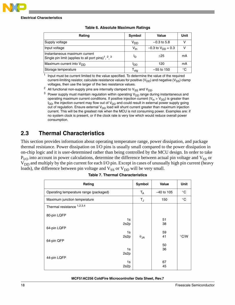
2.3 Thermal CharacteristicsThis section provides information about operating temperature range, power dissipation, and package thermal resistance. Power dissipation on I/O pins is usually small compared to the power dissipation in on-chip logic and it is user-determined rather than being controlled by the MCU design. In order to take PI/O into account in power calculations, determine the difference between actual pin voltage and VSS or VDD and multiply by the pin current for each I/O pin. Except in cases of unusually high pin current (heavy loads), the difference between pin voltage and VSS or VDD will be very small.
Table 6. Absolute Maximum Ratings
Rating Symbol Value Unit
Supply voltage VDD –0.3 to 5.8 V
Input voltage VIn –0.3 to VDD + 0.3 V
Instantaneous maximum current Single pin limit (applies to all port pins)1, 2, 3
1 Input must be current limited to the value specified. To determine the value of the required current-limiting resistor, calculate resistance values for positive (VDD) and negative (VSS) clamp voltages, then use the larger of the two resistance values.
2 All functional non-supply pins are internally clamped to VSS and VDD.3 Power supply must maintain regulation within operating VDD range during instantaneous and
operating maximum current conditions. If positive injection current (VIn > VDD) is greater than IDD, the injection current may flow out of VDD and could result in external power supply going out of regulation. Ensure external VDD load will shunt current greater than maximum injection current. This will be the greatest risk when the MCU is not consuming power. Examples are: if no system clock is present, or if the clock rate is very low which would reduce overall power consumption.
ID 25 mA
Maximum current into VDD IDD 120 mA
Storage temperature Tstg –55 to 150 C
Table 7. Thermal Characteristics
Rating Symbol Value Unit
Operating temperature range (packaged) TA –40 to 105 C
Maximum junction temperature TJ 150 C
Thermal resistance 1,2,3,4
80-pin LQFP1s
2s2p64-pin LQFP
1s2s2p
64-pin QFP
1s2s2p
44-pin LQFP1s
2s2p
JA
5138
5941
5036
6745
C/W
MCF51AC256 ColdFire Microcontroller Data Sheet, Rev.7
Freescale Semiconductor18

Electrical Characteristics
The average chip-junction temperature (TJ) in C can be obtained from:
TJ = TA + (PD JA) Eqn. 1
where:TA = Ambient temperature, CJA = Package thermal resistance, junction-to-ambient, C/WPD = Pint PI/OPint = IDD VDD, Watts — chip internal powerPI/O = Power dissipation on input and output pins — user determined
For most applications, PI/O Pint and can be neglected. An approximate relationship between PD and TJ (if PI/O is neglected) is:
PD = K (TJ + 273C) Eqn. 2
Solving Equation 1 and Equation 2 for K gives:
K = PD (TA + 273C) + JA (PD)2 Eqn. 3
where K is a constant pertaining to the particular part. K can be determined from Equation 3 by measuring PD (at equilibrium) for a known TA. Using this value of K, the values of PD and TJ can be obtained by solving Equation 1 and Equation 2 iteratively for any value of TA.
2.4 Electrostatic Discharge (ESD) Protection CharacteristicsAlthough damage from static discharge is much less common on these devices than on early CMOS circuits, normal handling precautions should be used to avoid exposure to static discharge. Qualification tests are performed to ensure that these devices can withstand exposure to reasonable levels of static without suffering any permanent damage.
All ESD testing is in conformity with CDF-AEC-Q00 Stress Test Qualification for Automotive Grade Integrated Circuits. (http://www.aecouncil.com/) This device was qualified to AEC-Q100 Rev E.
A device is considered to have failed if, after exposure to ESD pulses, the device no longer meets the device specification requirements. Complete dc parametric and functional testing is performed per the
1 Junction temperature is a function of die size, on-chip power dissipation, package thermal resistance, mounting site (board) temperature, ambient temperature, air flow, power dissipation of other components on the board, and board thermal resistance
2 Junction to Ambient Natural Convection3 1s — Single layer board, one signal layer4 2s2p — Four layer board, 2 signal and 2 power layers
MCF51AC256 ColdFire Microcontroller Data Sheet, Rev.7
Freescale Semiconductor 19
Electrical Characteristics
applicable device specification at room temperature followed by hot temperature, unless specified otherwise in the device specification.
2.5 DC CharacteristicsThis section includes information about power supply requirements, I/O pin characteristics, and power supply current in various operating modes.
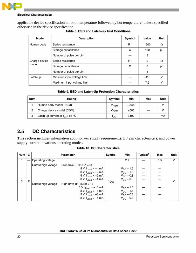
Table 8. ESD and Latch-up Test Conditions
Model Description Symbol Value Unit
Human body Series resistance R1 1500
Storage capacitance C 100 pF
Number of pulse per pin — 3
Charge device model
Series resistance R1 0
Storage capacitance C 0 pF
Number of pulse per pin — 3 —
Latch-up Minimum input voltage limit — –2.5 V
Maximum input voltage limit — 7.5 V
Table 9. ESD and Latch-Up Protection Characteristics
Num Rating Symbol Min Max Unit
1 Human body model (HBM) VHBM ±2000 — V
2 Charge device model (CDM) VCDM ±500 — V
3 Latch-up current at TA = 85 C ILAT ±100 — mA
Table 10. DC Characteristics
Num C Parameter Symbol Min Typical1 Max Unit
1 — Operating voltage 2.7 — 5.5 V
2 P
Output high voltage — Low drive (PTxDSn = 0)5 V, ILoad = –4 mA3 V, ILoad = –2 mA5 V, ILoad = –2 mA3 V, ILoad = –1 mA
VOH
VDD – 1.5VDD – 1.5VDD – 0.8VDD – 0.8
————
————
VOutput high voltage — High drive (PTxDSn = 1)
5 V, ILoad = –15 mA3 V, ILoad = –8 mA5 V, ILoad = –8 mA3 V, ILoad = –4 mA
VDD – 1.5VDD – 1.5VDD – 0.8VDD – 0.8
————
————
MCF51AC256 ColdFire Microcontroller Data Sheet, Rev.7
Freescale Semiconductor20
Electrical Characteristics
3 P
Output low voltage — Low Drive (PTxDSn = 0)5 V, ILoad = 4 mA3 V, ILoad = 2 mA5 V, ILoad = 2 mA3 V, ILoad = 1 mA
VOL
— —
1.51.50.80.8
VOutput low voltage — High Drive (PTxDSn = 1)
5 V, ILoad = 15 mA3 V, ILoad = 8 mA5 V, ILoad = 8 mA3 V, ILoad = 4 mA
— —
1.51.50.80.8
4 COutput high current — Max total IOH for all ports
5V3V
IOHT — —10060
mA
5 COutput low current — Max total IOL for all ports
5 V3 V
IOLT — —10060
mA
6 P Input high voltage; all digital inputs VIH 0.65 VDD — — V
P Input low voltage; all digital inputs VIL — — 0.35 VDD V7
D Input hysteresis; all digital inputs Vhys 0.06 VDD — — mV8
9 P Input leakage current; input only pins2 |IIn| — 0.1 1 A
10 P High impedance (off-state) leakage current2 |IOZ| — 0.1 1 A
11 P Internal pullup resistors3 RPU 20 45 65 k
12 P Internal pulldown resistors4 RPD 20 45 65 k
13 C Input capacitance; all non-supply pins CIn — — 8 pF
14 P POR rearm voltage VPOR 0.9 1.4 2.0 V
15 D POR rearm time tPOR 10 — — s
16 P
Low-voltage detection threshold —high range
VDD fallingVDD rising
VLVDH 4.24.27
4.354.4
4.54.6
V
P
Low-voltage detection threshold —low range
VDD fallingVDD rising
VLVDL 2.482.5
2.682.7
2.72.72
V17
P
Low-voltage warning threshold —high range
VDD fallingVDD rising
VLVWH 4.24.27
4.44.45
4.54.6
V18
19 P
Low-voltage warning threshold low range
VDD fallingVDD rising
VLVWL 2.482.5
2.682.7
2.72.72
V
20 TLow-voltage inhibit reset/recover hysteresis
5 V3 V
Vhys —10060
—mV
21 D RAM retention voltage VRAM — 0.6 1.0 V
Table 10. DC Characteristics (continued)
Num C Parameter Symbol Min Typical1 Max Unit
MCF51AC256 ColdFire Microcontroller Data Sheet, Rev.7
Freescale Semiconductor 21

Electrical Characteristics
Figure 5. Typical IOH vs. VDD–VOH at VDD = 3 V (Low Drive, PTxDSn = 0)
22 D
DC injection current5 6 7 8 (single pin limit)VIN >VDDVIN <VSS
IIC
00
—2
–0.2mA
DC injection current (Total MCU limit, includes sum of all stressed pins)
VIN >VDDVIN <VSS
00
— 25–5
mA
1 Typical values are based on characterization data at 25C unless otherwise stated.2 Measured with VIn = VDD or VSS.3 Measured with VIn = VSS.4 Measured with VIn = VDD.5 Power supply must maintain regulation within operating VDD range during instantaneous and operating maximum current
conditions. If positive injection current (VIn > VDD) is greater than IDD, the injection current may flow out of VDD and could result in external power supply going out of regulation. Ensure external VDD load will shunt current greater than maximum injection current. This will be the greatest risk when the MCU is not consuming power. Examples are: if no system clock is present, or if clock rate is very low (which would reduce overall power consumption).
6 All functional non-supply pins are internally clamped to VSS and VDD.7 Input must be current limited to the value specified. To determine the value of the required current-limiting resistor, calculate
resistance values for positive and negative clamp voltages, then use the larger of the two values.8 The RESET pin does not have a clamp diode to VDD. Do not drive this pin above VDD.
Table 10. DC Characteristics (continued)
Num C Parameter Symbol Min Typical1 Max Unit
–5.0E-3
–4.0E-3
–3.0E-3
–2.0E-3
–1.0E-3
000E+00 0.3 0.5 0.8 0.9 1.2 1.5
VDD–VOH (V)
VSupply–VOH
Average of IOH
I OH
(A)
25C
–6.0E-3
105C
-40C
MCF51AC256 ColdFire Microcontroller Data Sheet, Rev.7
Freescale Semiconductor22
Electrical Characteristics
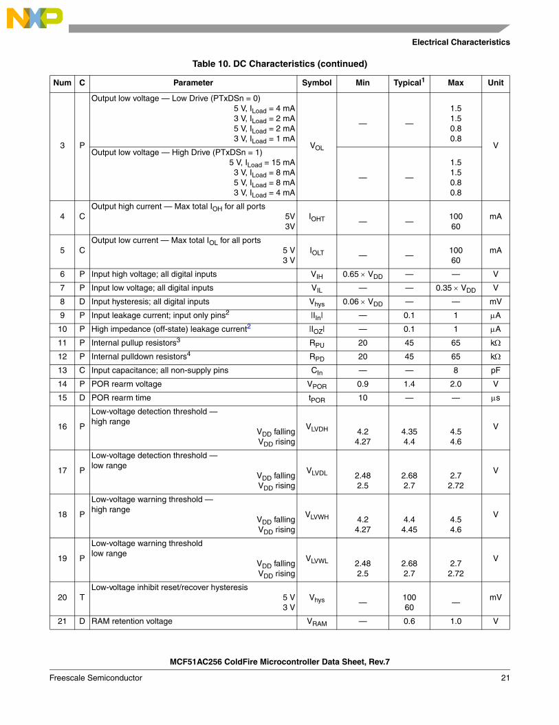
Figure 6. Typical IOH vs. VDD–VOH at VDD = 3 V (High Drive, PTxDSn = 1)
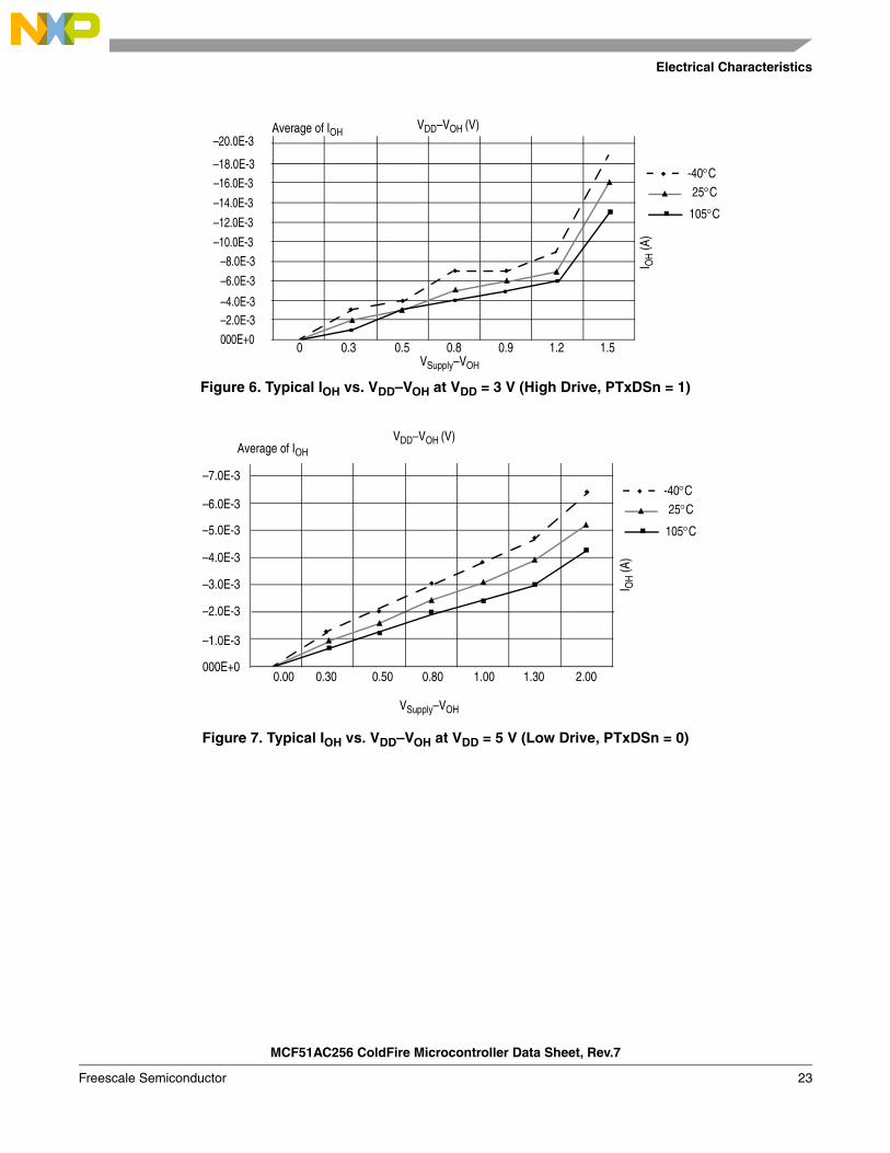
Figure 7. Typical IOH vs. VDD–VOH at VDD = 5 V (Low Drive, PTxDSn = 0)
–20.0E-3
–18.0E-3
–16.0E-3
–14.0E-3
–12.0E-3
–10.0E-3
–8.0E-3
–6.0E-3
–4.0E-3–2.0E-3
000E+00 0.3 0.5 0.8 0.9 1.2 1.5
VSupply–VOH
VDD–VOH (V)Average of IOH
I OH
(A)
25C
105C
-40C
–5.0E-3
–4.0E-3
–3.0E-3
–2.0E-3
–1.0E-3
000E+00.00 0.30
Average of IOH
–6.0E-3
–7.0E-3
0.50 0.80 1.00 1.30 2.00
VDD–VOH (V)
VSupply–VOH
I OH
(A)
25C
105C
-40C
MCF51AC256 ColdFire Microcontroller Data Sheet, Rev.7
Freescale Semiconductor 23

Electrical Characteristics
Figure 8. Typical IOH vs. VDD–VOH at VDD = 5 V (High Drive, PTxDSn = 1)
0.00 0.30 0.50 0.80 1.00 1.30 2.00
VSupply–VOH
–30.0E-3
–25.0E-3
–20.0E-3
–15.0E-3
–10.0E-3
–5.0E-3
000E+0
VDD–VOH (V)
I OH
(A)
Average of IOH
25C
105C
-40C
MCF51AC256 ColdFire Microcontroller Data Sheet, Rev.7
Freescale Semiconductor24

Electrical Characteristics
2.6 Supply Current CharacteristicsTable 11. Supply Current Characteristics
Num C Parameter Symbol VDD (V) Typical1 Max2 Unit
1 TRun supply current
measured at
FEI mode, all modules off, system clock at:
2 MHz
RIDD
5 2.27 —
mA
3.3 2.24 —
4 MHz5 3.67 —
3.3 3.64 —
8 MHz5 6.55 —
3.3 6.54 —
16 MHz5 11.90 —
3.3 11.85 —
2 TRun supply current
measured at
FEI mode, all modules on, system clock at:
2 MHz5 3.28 —
3.3 3.26 —
4 MHz5 4.33 —
3.3 4.32 —
8 MHz5 8.17 —
3.3 8.05 —
16 MHz5 14.8 —
3.3 14.74 —
3 TRun supply current
measured at
FBE mode, all modules off(RANGE = 1, HGO = 0), system clock at:
2 MHz5 3.28 —
3.3 3.26 —
4 MHz5 4.69 —
3.3 4.67 —
8 MHz5 7.48 —
3.3 7.46 —
16 MHz5 13.10 —
3.3 13.07 —
4 TRun supply current
measured at
FBE mode, all modules on(RANGE = 1, HGO = 0), system clock at:
2 MHz5 3.64 —
3.3 3.63 —
4 MHz5 5.38 —
3.3 5.35 —
8 MHz5 8.65 —
3.3 8.64 —
16 MHz5 15.55 —
3.3 15.40 —
MCF51AC256 ColdFire Microcontroller Data Sheet, Rev.7
Freescale Semiconductor 25
Electrical Characteristics
5 CWait mode supply3 current measured at
(CPU clock = 2 MHz, fBus = 1 MHz)
WIDD
5 1.3 2mA
3 1.29 2
6 CWait mode supply3 current measured at
(CPU clock = 16 MHz, fBus = 8 MHz)5 5.11 8
mA3 5.1 8
7 CWait mode supply3 current measured at
(CPU clock = 50 MHz, fBus = 25 MHz)5 15.24 25
mA3 15.2 25
8 C
Stop2 mode supply current –40 C25 C
120 C
–40 C25 C
120C
S2IDD
5 1.402.52.5200
A
3 1.162.52.5200
A
9 C
Stop3 mode supply current –40 C25 C
120C
–40 C25 C
120 C
S3IDD
5 1.602.52.5220
A
3 1.352.52.5220
A
10 C RTI adder to stop2 or stop33, 25 C S23IDDRTI5 300 nA
3 300 nA
11 CAdder to stop3 for oscillator enabled4
(ERCLKEN =1 and EREFSTEN = 1)S3IDDOSC 5, 3 5 A
1 Typicals are measured at 25 C.2 Values given here are preliminary estimates prior to completing characterization.3 Most customers are expected to find that auto-wakeup from stop2 or stop3 can be used instead of the higher current wait
mode. 4 Values given under the following conditions: low range operation (RANGE = 0), low power mode (HGO = 0).
Table 11. Supply Current Characteristics (continued)
Num C Parameter Symbol VDD (V) Typical1 Max2 Unit
MCF51AC256 ColdFire Microcontroller Data Sheet, Rev.7
Freescale Semiconductor26
Electrical Characteristics
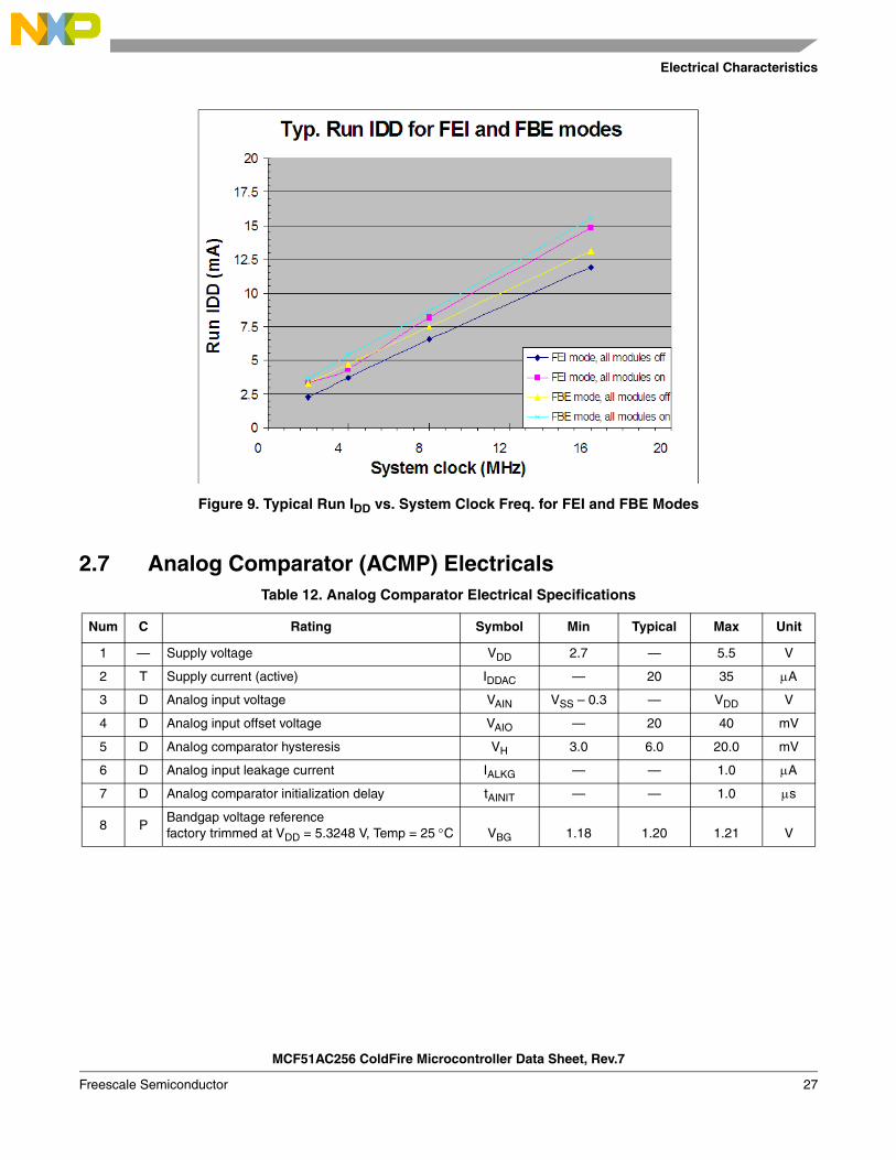
Figure 9. Typical Run IDD vs. System Clock Freq. for FEI and FBE Modes
2.7 Analog Comparator (ACMP) Electricals
Table 12. Analog Comparator Electrical Specifications
Num C Rating Symbol Min Typical Max Unit
1 — Supply voltage VDD 2.7 — 5.5 V
2 T Supply current (active) IDDAC — 20 35 A
3 D Analog input voltage VAIN VSS – 0.3 — VDD V
4 D Analog input offset voltage VAIO — 20 40 mV
5 D Analog comparator hysteresis VH 3.0 6.0 20.0 mV
6 D Analog input leakage current IALKG — — 1.0 A
7 D Analog comparator initialization delay tAINIT — — 1.0 s
8 PBandgap voltage referencefactory trimmed at VDD = 5.3248 V, Temp = 25 C VBG 1.18 1.20 1.21 V
MCF51AC256 ColdFire Microcontroller Data Sheet, Rev.7
Freescale Semiconductor 27
Electrical Characteristics
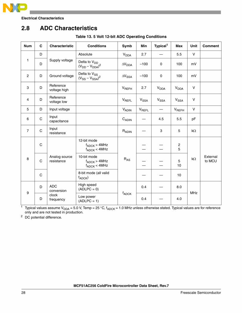
2.8 ADC CharacteristicsTable 13. 5 Volt 12-bit ADC Operating Conditions
Num C Characteristic Conditions Symb Min Typical1
1 Typical values assume VDDA = 5.0 V, Temp = 25 C, fADCK = 1.0 MHz unless otherwise stated. Typical values are for reference only and are not tested in production.
Max Unit Comment
1
D
Supply voltage
Absolute VDDA 2.7 — 5.5 V
DDelta to VDD (VDD – VDDA)2
2 DC potential difference.
VDDA –100 0 100 mV
2 D Ground voltageDelta to VSS (VSS – VSSA)2
VSSA –100 0 100 mV
3 DReference voltage high
VREFH 2.7 VDDA VDDA V
4 DReference voltage low
VREFL VSSA VSSA VSSA V
5 D Input voltage VADIN VREFL — VREFH V
6 CInput capacitance
CADIN — 4.5 5.5 pF
7 CInput resistance
RADIN — 3 5 k
8
C
Analog source resistance
12-bit modefADCK > 4MHzfADCK < 4MHz
RAS
——
——
25
kExternal to MCUC
10-bit modefADCK > 4MHzfADCK < 4MHz
——
——
510
C8-bit mode (all valid fADCK)
— — 10
9
D ADC conversion clock frequency
High speed (ADLPC = 0)
fADCK
0.4 — 8.0
MHz
DLow power (ADLPC = 1)
0.4 — 4.0
MCF51AC256 ColdFire Microcontroller Data Sheet, Rev.7
Freescale Semiconductor28
Electrical Characteristics
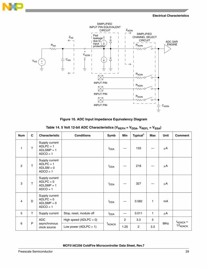
Figure 10. ADC Input Impedance Equivalency Diagram
Table 14. 5 Volt 12-bit ADC Characteristics (VREFH = VDDA, VREFL = VSSA)
Num C Characteristic Conditions Symb Min Typical1 Max Unit Comment
1 T
Supply currentADLPC = 1 ADLSMP = 1 ADCO = 1
IDDA — 133 — A
2 T
Supply currentADLPC = 1 ADLSM = 0 ADCO = 1
IDDA — 218 — A
3 T
Supply current ADLPC = 0 ADLSMP = 1 ADCO = 1
IDDA — 327 — A
4 D
Supply current ADLPC = 0 ADLSMP = 0 ADCO = 1
IDDA — 0.582 1 mA
5 T Supply current Stop, reset, module off IDDA — 0.011 1 A
6 PADC asynchronous clock source
High speed (ADLPC = 0)fADACK
2 3.3 5MHz
tADACK = 1/fADACKLow power (ADLPC = 1) 1.25 2 3.3
+–
+
–VAS
RAS
CAS
VADIN
ZASPad leakagedue toinput protection
ZADIN
SIMPLIFIED INPUT PIN EQUIVALENT
CIRCUIT
RADIN
ADC SARENGINE
SIMPLIFIED CHANNEL SELECT
CIRCUIT
INPUT PIN
RADIN
CADIN
INPUT PIN
RADIN
INPUT PIN
RADIN
MCF51AC256 ColdFire Microcontroller Data Sheet, Rev.7
Freescale Semiconductor 29

Electrical Characteristics
7 PConversion time (including sample time)
Short sample (ADLSMP = 0)tADC
— 20 —ADCK cycles
See Table 10
for conversion
time variances
Long sample (ADLSMP = 1) — 40 —
8 T Sample timeShort sample (ADLSMP = 0)
tADS
— 3.5 — ADCK cyclesLong sample (ADLSMP = 1) — 23.5 —
9
TTotal unadjusted error
12-bit mode
ETUE
— 3.0 —
LSB2Includes
quantization
P 10-bit mode — 1 2.5
T 8-bit mode — 0.5 1.0
10
T
Differential non-linearity
12-bit mode
DNL
— 1.75 —
LSB2P 10-bit mode3 — 0.5 1.0
T 8-bit mode3 — 0.3 0.5
11
T
Integral non-linearity
12-bit mode
INL
— 1.5 —
LSB2T 10-bit mode — 0.5 1.0
T 8-bit mode — 0.3 0.5
12
T
Zero-scale error
12-bit mode
EZS
— 1.5 —
LSB2 VADIN = VSSA
P 10-bit mode — 0.5 1.5
T 8-bit mode — 0.5 0.5
13
T
Full-scale error
12-bit mode
EFS
— 1 —
LSB2 VADIN = VDDA
P 10-bit mode — 0.5 1
T 8-bit mode — 0.5 0.5
14 DQuantization error
12-bit mode
EQ
— –1 to 0 —
LSB210-bit mode — — 0.5
8-bit mode — — 0.5
15 DInput leakage error
12-bit mode
EIL
— 1 —
LSB2Pad
leakage4 * RAS
10-bit mode — 0.2 2.5
8-bit mode — 0.1 1
16 DTemp sensor voltage
25C VTEMP25 — 1.396 — V
17 DTemp sensor slope
–40 C–25 Cm
— 3.266 —mV/C
25 C–85 C — 3.638 —
1 Typical values assume VDDA = 5.0 V, Temp = 25 C, fADCK = 1.0 MHz unless otherwise stated. Typical values are for reference only and are not tested in production.
2 1 LSB = (VREFH – VREFL)/2N.
Table 14. 5 Volt 12-bit ADC Characteristics (VREFH = VDDA, VREFL = VSSA) (continued)
Num C Characteristic Conditions Symb Min Typical1 Max Unit Comment
MCF51AC256 ColdFire Microcontroller Data Sheet, Rev.7
Freescale Semiconductor30
Electrical Characteristics
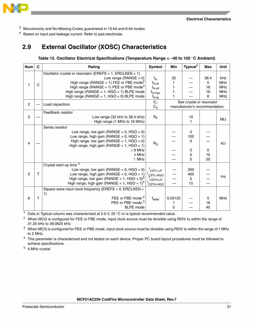
2.9 External Oscillator (XOSC) Characteristics
3 Monotonicity and No-Missing-Codes guaranteed in 10-bit and 8-bit modes4 Based on input pad leakage current. Refer to pad electricals.
Table 15. Oscillator Electrical Specifications (Temperature Range = –40 to 105 C Ambient)
Num C Rating Symbol Min Typical1
1 Data in Typical column was characterized at 5.0 V, 25 C or is typical recommended value.
Max Unit
1 C
Oscillator crystal or resonator (EREFS = 1, ERCLKEN = 1) Low range (RANGE = 0)
High range (RANGE = 1) FEE or FBE mode2
High range (RANGE = 1) PEE or PBE mode3
High range (RANGE = 1, HGO = 1) BLPE mode High range (RANGE = 1, HGO = 0) BLPE mode
2 When MCG is configured for FEE or FBE mode, input clock source must be divisible using RDIV to within the range of 31.25 kHz to 39.0625 kHz.
3 When MCG is configured for PEE or PBE mode, input clock source must be divisible using RDIV to within the range of 1 MHz to 2 MHz.
flofhi-fllfhi-pllfhi-hgofhi-lp
321111
—————
38.45
16168
kHzMHzMHzMHzMHz
2 — Load capacitorsC1C2
See crystal or resonator manufacturer’s recommendation.
3 —Feedback resistor
Low range (32 kHz to 38.4 kHz)High range (1 MHz to 16 MHz)
RF 101
M
4 —
Series resistorLow range, low gain (RANGE = 0, HGO = 0)
Low range, high gain (RANGE = 0, HGO = 1)High range, low gain (RANGE = 1, HGO = 0)
High range, high gain (RANGE = 1, HGO = 1) 8 MHz MHz MHz
RS
———
———
01000
000
———
01020
k
5 T
Crystal start-up time 4
Low range, low gain (RANGE = 0, HGO = 0)Low range, high gain (RANGE = 0, HGO = 1)High range, low gain (RANGE = 1, HGO = 0)5
High range, high gain (RANGE = 1, HGO = 1)5
4 This parameter is characterized and not tested on each device. Proper PC board layout procedures must be followed to achieve specifications.
5 4 MHz crystal
tCSTL-LP
tCSTL-HGOtCSTH-LP
tCSTH-HGO
— — — —
2004005
15
————
ms
6 T
Square wave input clock frequency (EREFS = 0, ERCLKEN = 1)
FEE or FBE mode 2
PEE or PBE mode 3
BLPE mode
fextal 0.0312510
———
51640
MHz
MCF51AC256 ColdFire Microcontroller Data Sheet, Rev.7
Freescale Semiconductor 31

Electrical Characteristics
2.10 MCG SpecificationsTable 16. MCG Frequency Specifications (Temperature Range = –40 to 105 C Ambient)
Num C Rating Symbol Min Typical1 Max Unit
1 CInternal reference frequency — factory trimmed at VDD = 5 V and temperature = 25 C fint_ft — 32.768 — kHz
2 C Average internal reference frequency — untrimmed fint_ut 31.25 — 39.0625 kHz
3 T Internal reference startup time tirefst — 60 100 s
4
CDCO output frequency range — untrimmed 2
Low range (DRS=00)
fdco_ut
16 — 20
MHzC Mid range (DRS=01) 32 — 40
C High range (DRS=10) 48 — 60
5
P DCO output frequency2 reference =32768Hzand DMX32 = 1
Low range (DRS=00)
fdco_DMX32
— 16.82 —
MHzP Mid range (DRS=01) — 33.69 —
P High range (DRS=10) — 50.48 —
6 DResolution of trimmed DCO output frequency at fixed voltage and temperature (using FTRIM)
fdco_res_t — 0.1 0.2 %fdco
7 DResolution of trimmed DCO output frequency at fixed voltage and temperature (not using FTRIM)
fdco_res_t — 0.2 0.4 %fdco
8 DTotal deviation of trimmed DCO output frequency over voltage and temperature
fdco_t —0.5
–1.02 %fdco
9 DTotal deviation of trimmed DCO output frequency over fixed voltage and temperature range of 0–70 C fdco_t — 0.5 1 %fdco
10 D FLL acquisition time3 tfll_acquire — — 1 ms
11 D PLL acquisition time4 tpll_acquire — — 1 ms
12 DLong term jitter of DCO output clock (averaged over 2ms interval) 5
CJitter — 0.02 0.2 %fdco
13 D VCO operating frequency fvco 7.0 — 55.0 MHz
16 D Jitter of PLL output clock measured over 625 ns6 fpll_jitter_625ns — 0.5666 — %fpll
17 D Lock entry frequency tolerance 7 Dlock 1.49 — 2.98 %
MCU
EXTAL XTAL
Crystal or Resonator
RS
C2
RF
C1
MCF51AC256 ColdFire Microcontroller Data Sheet, Rev.7
Freescale Semiconductor32

Electrical Characteristics
o
2.11 AC CharacteristicsThis section describes ac timing characteristics for each peripheral system.
18 D Lock exit frequency tolerance 8 Dunl 4.47 — 5.97 %
19 D Lock time — FLL tfll_lock — —tfll_acquire+
1075(1/fint_t)s
20 D Lock time — PLL tpll_lock — —tpll_acquire+
1075(1/fpll_ref)s
21 DLoss of external clock minimum frequency — RANGE = 0 floc_low (3/5) fint — — kHz
1 Data in Typical column was characterized at 5.0 V, 25 C or is typical recommended value.2 The resulting bus clock frequency must not exceed the maximum specified bus clock frequency of the device.3 This specification applies when the FLL reference source or reference divider is changed, trim value changed or changing from
FLL disabled (BLPE, BLPI) to FLL enabled (FEI, FEE, FBE, FBI). If a crystal/resonator is being used as the reference, this specification assumes it is already running.
4 This specification applies when the PLL VCO divider or reference divider is changed, or changing from PLL disabled (BLPE, BLPI) to PLL enabled (PBE, PEE). If a crystal/resonator is being used as the reference, this specification assumes it is already running.
5 Jitter is the average deviation from the programmed frequency measured over the specified interval at maximum fBUS. Measurements are made with the device powered by filtered supplies and clocked by a stable external clock signal. Noise injected into the FLL circuitry via VDD and VSS and variation in crystal oscillator frequency increase the CJitter percentage for a given interval.
6 625 ns represents 5 time quanta for CAN applications, under worst case conditions of 8 MHz CAN bus clock, 1 Mbps CAN bus speed, and 8 time quanta per bit for bit time settings. 5 time quanta is the minimum time between a synchronization edge and the sample point of a bit using 8 time quanta per bit.
7 Below Dlock minimum, the MCG enters lock. Above Dlock maximum, the MCG will not enter lock. But if the MCG is already in lock, then the MCG may stay in lock.
8 Below Dunl minimum, the MCG will not exit lock if already in lock. Above Dunl maximum, the MCG is guaranteed to exit lock.
Table 16. MCG Frequency Specifications (continued)(Temperature Range = –40 to 105 C Ambient)
Num C Rating Symbol Min Typical1 Max Unit
MCF51AC256 ColdFire Microcontroller Data Sheet, Rev.7
Freescale Semiconductor 33

Electrical Characteristics
2.11.1 Control Timing
Figure 11. Reset Timing
Figure 12. IRQ/KBIPx Timing
Table 17. Control Timing
Num C Parameter Symbol Min Typical1
1 Typical values are based on characterization data at VDD = 5.0 V, 25 C unless otherwise stated.
Max Unit
1 D Bus frequency (tcyc = 1/fBus) fBus dc — 24 MHz
2 D Internal low-power oscillator period tLPO 800 — 1500 s
3 DExternal reset pulse width2
(tcyc = 1/fSelf_reset)
2 This is the shortest pulse that is guaranteed to be recognized as a reset pin request. Shorter pulses are not guaranteed to override reset requests from internal sources.
textrst 100 — — ns
4 D Reset low drive trstdrv 66 tcyc — — ns
5 D Active background debug mode latch setup time tMSSU 500 — — ns
6 D Active background debug mode latch hold time tMSH 100 — — ns
7 DIRQ pulse width
Asynchronous path2
Synchronous path3
3 This is the minimum pulse width that is guaranteed to pass through the pin synchronization circuitry. Shorter pulses may or may not be recognized. In stop mode, the synchronizer is bypassed so shorter pulses can be recognized in that case.
tILIH, tIHIL100
1.5 tcyc— — ns
8 DKBIPx pulse width
Asynchronous path2
Synchronous path3 tILIH, tIHIL100
1.5 tcyc— — ns
9 D
Port rise and fall time (load = 50 pF)4
Slew rate control disabled (PTxSE = 0), Low Drive Slew rate control enabled (PTxSE = 1), Low DriveSlew rate control disabled (PTxSE = 0), Low Drive
Slew rate control enabled (PTxSE = 1), Low Drive
4 Timing is shown with respect to 20% VDD and 80% VDD levels. Temperature range –40 C to 105 C.
tRise, tFall
————
11354075
— ns
textrst
RESET PIN
tIHIL
IRQ/KBIPx
tILIH
IRQ/KBIPx
MCF51AC256 ColdFire Microcontroller Data Sheet, Rev.7
Freescale Semiconductor34
Electrical Characteristics
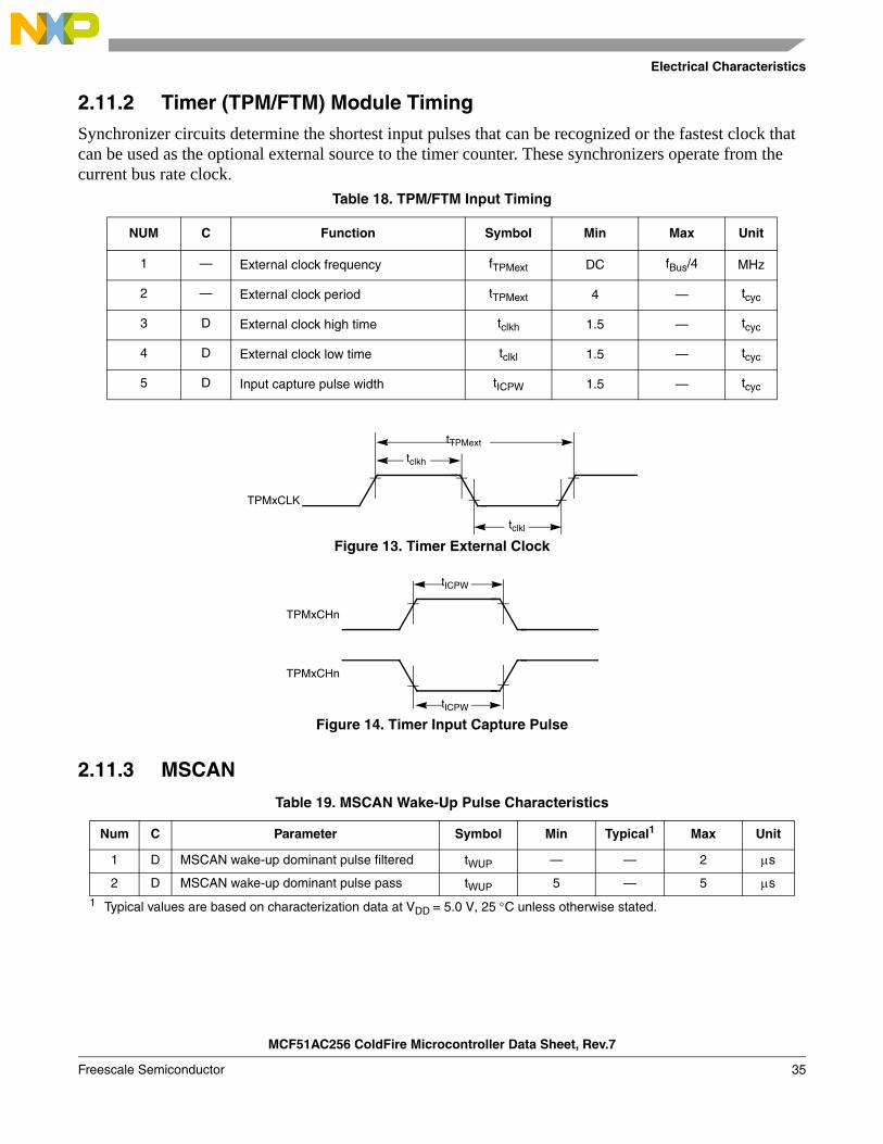
2.11.2 Timer (TPM/FTM) Module TimingSynchronizer circuits determine the shortest input pulses that can be recognized or the fastest clock that can be used as the optional external source to the timer counter. These synchronizers operate from the current bus rate clock.
Figure 13. Timer External Clock
Figure 14. Timer Input Capture Pulse
2.11.3 MSCAN
Table 18. TPM/FTM Input Timing
NUM C Function Symbol Min Max Unit
1 — External clock frequency fTPMext DC fBus/4 MHz
2 — External clock period tTPMext 4 — tcyc
3 D External clock high time tclkh 1.5 — tcyc
4 D External clock low time tclkl 1.5 — tcyc
5 D Input capture pulse width tICPW 1.5 — tcyc
Table 19. MSCAN Wake-Up Pulse Characteristics
Num C Parameter Symbol Min Typical1
1 Typical values are based on characterization data at VDD = 5.0 V, 25 C unless otherwise stated.
Max Unit
1 D MSCAN wake-up dominant pulse filtered tWUP — — 2 s
2 D MSCAN wake-up dominant pulse pass tWUP 5 — 5 s
tTPMext
tclkh
tclkl
TPMxCLK
tICPW
TPMxCHn
tICPW
TPMxCHn
MCF51AC256 ColdFire Microcontroller Data Sheet, Rev.7
Freescale Semiconductor 35

Electrical Characteristics
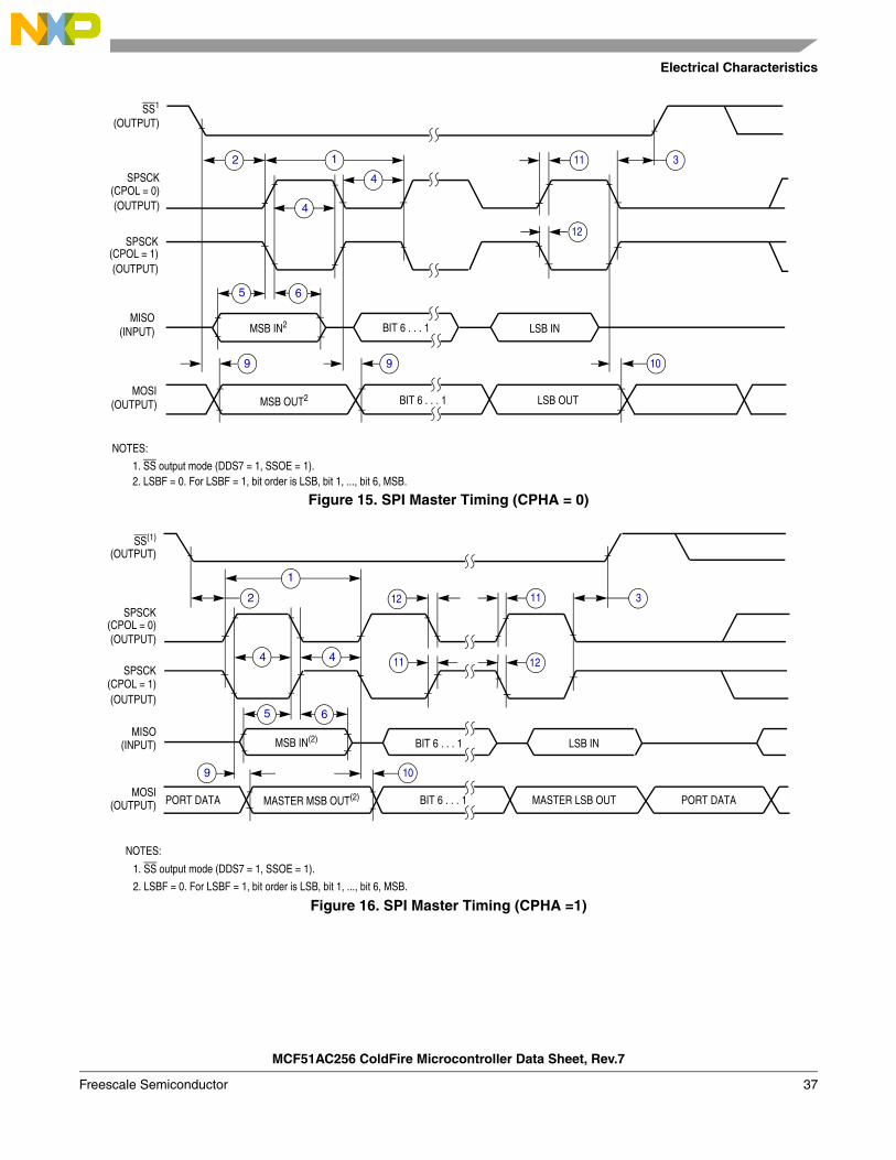
2.12 SPI CharacteristicsTable 20 and Figure 15 through Figure 18 describe the timing requirements for the SPI system.
Table 20. SPI Timing
No. C Function Symbol Min Max Unit
— DOperating frequency
MasterSlave
fop fBus/20480
fBus/2fBus/4
Hz
1 DSPSCK period
MasterSlave
tSPSCK 24
2048—
tcyctcyc
2 DEnable lead time
MasterSlave
tLead 121
——
tSPSCKtcyc
3 DEnable lag time
MasterSlave
tLag 121
——
tSPSCKtcyc
4 DClock (SPSCK) high or low time
MasterSlave
tWSPSCK tcyc –30tcyc – 30
1024 tcyc—
nsns
5 DData setup time (inputs)
MasterSlave
tSU 1515
——
nsns
6 DData hold time (inputs)
MasterSlave
tHI 025
——
nsns
7 D Slave access time ta — 1 tcyc
8 D Slave MISO disable time tdis — 1 tcyc
9 DData valid (after SPSCK edge)
MasterSlave
tv ——
2525
nsns
10 DData hold time (outputs)
MasterSlave
tHO 00
——
nsns
11 DRise time
InputOutput
tRItRO
——
tcyc – 2525
nsns
12 DFall time
InputOutput
tFItFO
——
tcyc – 2525
nsns
MCF51AC256 ColdFire Microcontroller Data Sheet, Rev.7
Freescale Semiconductor36
Electrical Characteristics
Figure 15. SPI Master Timing (CPHA = 0)
Figure 16. SPI Master Timing (CPHA =1)
SPSCK
(OUTPUT)
SPSCK
(OUTPUT)
MISO(INPUT)
MOSI(OUTPUT)
SS1
(OUTPUT)
MSB IN2
BIT 6 . . . 1
LSB IN
MSB OUT2 LSB OUT
BIT 6 . . . 1
(CPOL = 0)
(CPOL = 1)
NOTES:
2. LSBF = 0. For LSBF = 1, bit order is LSB, bit 1, ..., bit 6, MSB.1. SS output mode (DDS7 = 1, SSOE = 1).
12 3
4
5 6
9 10
11
12
4
9
SPSCK
(OUTPUT)
SPSCK
(OUTPUT)
MISO(INPUT)
MOSI(OUTPUT)
MSB IN(2)
BIT 6 . . . 1
LSB IN
MASTER MSB OUT(2) MASTER LSB OUT
BIT 6 . . . 1
PORT DATA
(CPOL = 0)
(CPOL = 1)
PORT DATA
SS(1)
(OUTPUT)
1. SS output mode (DDS7 = 1, SSOE = 1).
2. LSBF = 0. For LSBF = 1, bit order is LSB, bit 1, ..., bit 6, MSB.
NOTES:
2
1
12 11 3
4 4 11 12
5 6
9 10
MCF51AC256 ColdFire Microcontroller Data Sheet, Rev.7
Freescale Semiconductor 37

Electrical Characteristics
Figure 17. SPI Slave Timing (CPHA = 0)
Figure 18. SPI Slave Timing (CPHA = 1)
2.13 Flash SpecificationsThis section provides details about program/erase times and program-erase endurance for the Flash memory.
Program and erase operations do not require any special power sources other than the normal VDD supply. For more detailed information about program/erase operations, see Chapter 4, “Memory.”
SPSCK
(INPUT)
SPSCK
(INPUT)
MOSI(INPUT)
MISO(OUTPUT)
SS(INPUT)
MSB IN
BIT 6 . . . 1
LSB IN
MSB OUT SLAVE LSB OUT
BIT 6 . . . 1
(CPOL = 0)
(CPOL = 1)
NOTE:
SLAVESEE
NOTE
1. Not defined but normally MSB of character just received
1
2
3
4
5 6
7
8
9 10
1112
411 12
10
SPSCK
(INPUT)
SPSCK
(INPUT)
MOSI(INPUT)
MISO(OUTPUT)
MSB IN
BIT 6 . . . 1
LSB IN
MSB OUT SLAVE LSB OUT
BIT 6 . . . 1
SEE
(CPOL = 0)
(CPOL = 1)
SS(INPUT)
NOTE:
SLAVE NOTE
1. Not defined but normally LSB of character just received
1
2
3
4
5 67
89 10
1112
4 11 12
MCF51AC256 ColdFire Microcontroller Data Sheet, Rev.7
Freescale Semiconductor38

Electrical Characteristics
2.14 EMC PerformanceElectromagnetic compatibility (EMC) performance is highly dependant on the environment in which the MCU resides. Board design and layout, circuit topology choices, location and characteristics of external components as well as MCU software operation all play a significant role in EMC performance. The system designer should consult Freescale applications notes such as AN2321, AN1050, AN1263, AN2764, and AN1259 for advice and guidance specifically targeted at optimizing EMC performance.
2.14.1 Radiated EmissionsMicrocontroller radiated RF emissions are measured from 150 kHz to 1 GHz using the TEM/GTEM Cell method in accordance with the IEC 61967-2 and SAE J1752/3 standards. The measurement is performed with the microcontroller installed on a custom EMC evaluation board while running specialized EMC test software. The radiated emissions from the microcontroller are measured in a TEM cell in two package orientations (North and East). For more detailed information concerning the evaluation results, conditions and setup, please refer to the EMC Evaluation Report for this device.
Table 21. Flash Characteristics
Num C Characteristic Symbol Min Typical1
1 Typical values are based on characterization data at VDD = 5.0 V, 25 C unless otherwise stated.
Max Unit
1 — Supply voltage for program/erase Vprog/erase 2.7 — 5.5 V
2 — Supply voltage for read operation VRead 2.7 — 5.5 V
3 — Internal FCLK frequency2
2 The frequency of this clock is controlled by a software setting.
fFCLK 150 — 200 kHz
4 — Internal FCLK period (1/FCLK) tFcyc 5 — 6.67 s
5 — Byte program time (random location)2 tprog 9 tFcyc
6 — Byte program time (burst mode)2 tBurst 4 tFcyc
7 — Page erase time3
3 These values are hardware state machine controlled. User code does not need to count cycles. This information supplied for calculating approximate time to program and erase.
tPage 4000 tFcyc
8 — Mass erase time2 tMass 20,000 tFcyc
9 CProgram/erase endurance4
TL to TH = –40 C to 105 CT = 25 C
4 Typical endurance for flash was evaluated for this product family on the 9S12Dx64. For additional information on how Freescale Semiconductor defines typical endurance, please refer to Engineering Bulletin EB619/D, Typical Endurance for Nonvolatile Memory.
— 10,000—
—100,000
——
cycles
10 C Data retention5
5 Typical data retention values are based on intrinsic capability of the technology measured at high temperature and de-rated to 25C using the Arrhenius equation. For additional information on how Freescale Semiconductor defines typical data retention, please refer to Engineering Bulletin EB618/D, Typical Data Retention for Nonvolatile Memory.
tD_ret 15 100 — years
MCF51AC256 ColdFire Microcontroller Data Sheet, Rev.7
Freescale Semiconductor 39
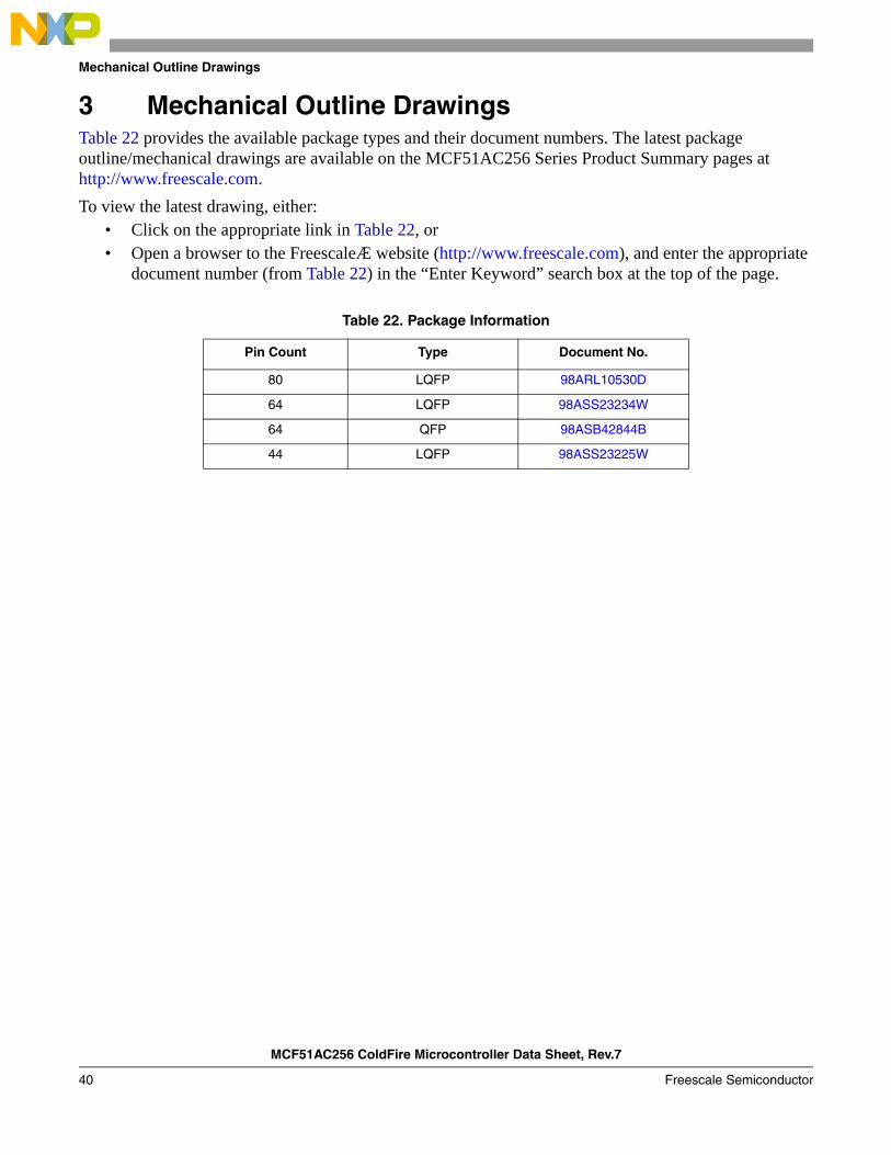
Mechanical Outline Drawings
3 Mechanical Outline DrawingsTable 22 provides the available package types and their document numbers. The latest package outline/mechanical drawings are available on the MCF51AC256 Series Product Summary pages at http://www.freescale.com.
To view the latest drawing, either:• Click on the appropriate link in Table 22, or• Open a browser to the FreescaleÆ website (http://www.freescale.com), and enter the appropriate
document number (from Table 22) in the “Enter Keyword” search box at the top of the page.
Table 22. Package Information
Pin Count Type Document No.
80 LQFP 98ARL10530D
64 LQFP 98ASS23234W
64 QFP 98ASB42844B
44 LQFP 98ASS23225W
MCF51AC256 ColdFire Microcontroller Data Sheet, Rev.7
Freescale Semiconductor40

Revision History
4 Revision HistoryTable 23. Revision History
Revision Description
1 Initial published
2 Updated ADC channels, Item 1, 4-5 on Table 2.10
3 Completed all theTBDs. Changed RTC to RTI in Figure 1. Corrected the block diagram.Changed VDDAD to VDDA, VSSAD to VSSA.Added charge device model data and removed machine data in Table 8.Updated the specifications of VLVDH, VLVDL, VLVWH and VLVWL in Table 10.Updated S2IDD, S3IDD in Table 11.Added C column in Table 14.Updated fdco_DMX32 in Table 16.
4 Corrected the expansion of SPI to serial peripheral interface.
5 Updated VLVDL in the Table 10.Updated RIDD in the Table 11.
6 Updated VLVDH, VLVDL, VLVWH and VLVWL in the Table 10.Added LPO on the Figure 1 and LPO features in the Section 1.3, “Features.”
7 Added 44-pin LQFP package information for AC256 and AC128.
MCF51AC256 ColdFire Microcontroller Data Sheet, Rev.7
Freescale Semiconductor 41

How to Reach Us:
Home Page:www.freescale.com
Web Support:http://www.freescale.com/support
USA/Europe or Locations Not Listed:Freescale Semiconductor, Inc.Technical Information Center, EL5162100 East Elliot RoadTempe, Arizona 852841-800-521-6274 or +1-480-768-2130www.freescale.com/support
Europe, Middle East, and Africa:Freescale Halbleiter Deutschland GmbHTechnical Information CenterSchatzbogen 781829 Muenchen, Germany+44 1296 380 456 (English)+46 8 52200080 (English)+49 89 92103 559 (German)+33 1 69 35 48 48 (French)www.freescale.com/support
Japan:Freescale Semiconductor Japan Ltd.HeadquartersARCO Tower 15F1-8-1, Shimo-Meguro, Meguro-ku,Tokyo 153-0064Japan0120 191014 or +81 3 5437 [email protected]
Asia/Pacific:Freescale Semiconductor China Ltd.Exchange Building 23FNo. 118 Jianguo RoadChaoyang DistrictBeijing 100022 China +86 10 5879 [email protected]
For Literature Requests Only:Freescale Semiconductor Literature Distribution CenterP.O. Box 5405Denver, Colorado 802171-800-441-2447 or +1-303-675-2140Fax: [email protected]
Freescale™ and the Freescale logo are trademarks ofFreescale Semiconductor, Inc. All other product or service namesare the property of their respective owners.
Information in this document is provided solely to enable system and software implementers to use Freescale Semiconductor products. There are no express or implied copyright licenses granted hereunder to design or fabricate any integrated circuits or integrated circuits based on the information in this document.
Freescale Semiconductor reserves the right to make changes without further notice to any products herein. Freescale Semiconductor makes no warranty, representation or guarantee regarding the suitability of its products for any particular purpose, nor does Freescale Semiconductor assume any liability arising out of the application or use of any product or circuit, and specifically disclaims any and all liability, including without limitation consequential or incidental damages. “Typical” parameters that may be provided in Freescale Semiconductor data sheets and/or specifications can and do vary in different applications and actual performance may vary over time. All operating parameters, including “Typicals”, must be validated for each customer application by customer’s technical experts. Freescale Semiconductor does not convey any license under its patent rights nor the rights of others. Freescale Semiconductor products are not designed, intended, or authorized for use as components in systems intended for surgical implant into the body, or other applications intended to support or sustain life, or for any other application in which the failure of the Freescale Semiconductor product could create a situation where personal injury or death may occur. Should Buyer purchase or use Freescale Semiconductor products for any such unintended or unauthorized application, Buyer shall indemnify and hold Freescale Semiconductor and its officers, employees, subsidiaries, affiliates, and distributors harmless against all claims, costs, damages, and expenses, and reasonable attorney fees arising out of, directly or indirectly, any claim of personal injury or death associated with such unintended or unauthorized use, even if such claim alleges that Freescale Semiconductor was negligent regarding the design or manufacture of the part.
© Freescale Semiconductor, Inc. 2008-2010. All rights reserved.
MCF51AC256Rev.79/2011