mcp3550/1/3 low-power, single-channel 22-bit delta-sigma adcs fileare 2.7v to 5.5v low-power, 22-bit...
TRANSCRIPT

MCP3550/1/3Low-Power, Single-Channel 22-Bit Delta-Sigma ADCs
Features
• 22-bit ADC in Small 8-pin MSOP Package with Automatic Internal Offset and Gain Calibration
• Low-Output Noise of 2.5 µVRMS with Effective Resolution of 21.9 bits (MCP3550/1)
• 3 µV Typical Offset Error
• 2 ppm Typical Full-Scale Error • 6 ppm Maximum INL Error• Total Unadjusted Error Less Than 10 ppm
• No Digital Filter Settling Time, Single-Command Conversions through 3-wire SPI Interface
• Ultra-Low Conversion Current (MCP3550/1):- 100 µA typical (VDD = 2.7V)- 120 µA typical (VDD = 5.0V)
• Differential Input with VSS to VDD Common Mode Range
• 2.7V to 5.5V Single-Supply Operation• Extended Temperature Range:
- -40°C to +125°C
Applications
• Weigh Scales
• Direct Temperature Measurement• 6-digit DVMs• Instrumentation
• Data Acquisition• Strain Gauge Measurement
Block Diagram
Description
The Microchip Technology Inc. MCP3550/1/3 devicesare 2.7V to 5.5V low-power, 22-bit Delta-Sigma Ana-log-to-Digital Converters (ADCs). The devices offeroutput noise as low as 2.5 µVRMS, with a totalunadjusted error of 10 ppm. The family exhibits 6 ppmIntegral Non-Linearity (INL) error, 3 µV offset error andless than 2 ppm full-scale error. The MCP3550/1/3devices provide high accuracy and low noiseperformance for applications where sensormeasurements (such as pressure, temperature andhumidity) are performed. With the internal oscillatorand high oversampling rate, minimal externalcomponents are required for high-accuracyapplications.
This product line has fully differential analog inputs,making it compatible with a wide variety of sensor,industrial control or process control applications.
The MCP3550/1/3 devices operate from -40°C to+125°C and are available in the space-saving 8-pinMSOP and SOIC packages.
Package Types:
Device Selection TableVSS
VIN+
VIN-
SCK
VDD
SDO
CS
SIN
C 4
Internal
Ser
ial I
nter
face
VREF
POROscillator
3rd-OrderDS ADC Modulatorw/ Internal Calibration
VDD
RDY
Part NumberSample
RateEffective
Resolution50/60 Hz Rejection
MCP3550-50 12.5 sps 21.9 bits 50 Hz
MCP3550-60 15 sps 21.9 bits 60 Hz
MCP3551 13.75 sps 21.9 bits 50/60 Hz (simultaneous)
MCP3553 60 sps 20.6 bits N/A
VIN–
VIN+
MCP3550/1/3
VSS
CS
SDO/RDY
1
2
3
4
8
7
6
5 SCK
VDDVREF
SOIC, MSOP
© 2007 Microchip Technology Inc. DS21950D-page 1

MCP3550/1/3
1.0 ELECTRICAL CHARACTERISTICS
1.1 Maximum Ratings*
VDD...................................................................................7.0V
All inputs and outputs w.r.t VSS .............. -0.3V to VDD + 0.3V
Difference Input Voltage ....................................... |VDD - VSS|
Output Short Circuit Current .................................Continuous
Current at Input Pins ....................................................±2 mA
Current at Output and Supply Pins ............................±10 mA
Storage Temperature.....................................-65°C to +150°C
Ambient temp. with power applied ................-55°C to +125°C
ESD protection on all pins (HBM, MM) ............ ≥ 6 kV, ≥ 400V
Maximum Junction Temperature (TJ) . .........................+150°C
† Notice: Stresses above those listed under "MaximumRatings" may cause permanent damage to the device. This isa stress rating only and functional operation of the device atthose or any other conditions above those indicated in theoperation listings of this specification is not implied. Exposureto maximum rating conditions for extended periods may affectdevice reliability.
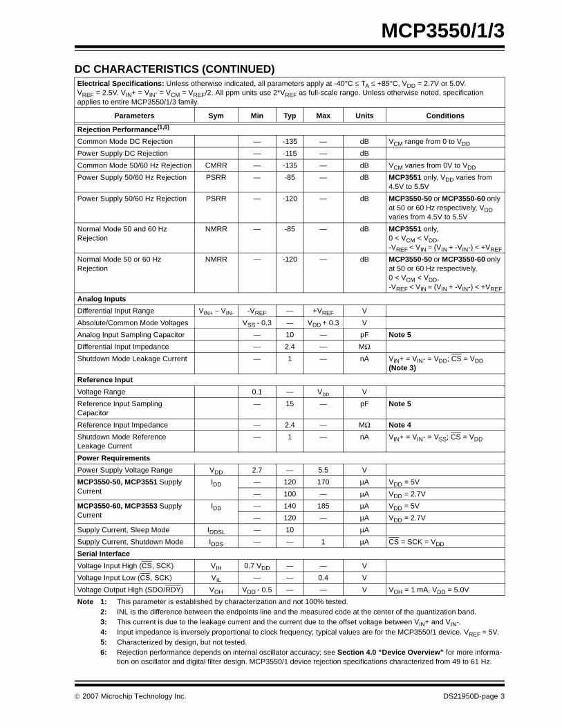
DC CHARACTERISTICSElectrical Specifications: Unless otherwise indicated, all parameters apply at -40°C ≤ TA ≤ +85°C, VDD = 2.7V or 5.0V. VREF = 2.5V. VIN+ = VIN- = VCM = VREF/2. All ppm units use 2*VREF as full-scale range. Unless otherwise noted, specification applies to entire MCP3550/1/3 family.
Parameters Sym Min Typ Max Units Conditions
Noise Performance (MCP3550/1)
No Missing Codes NMC 22 — — bits At DC (Note 5)
Output Noise eN — 2.5 — µVRMS
Effective Resolution ER — 21.9 — bits RMS VREF = 5V
Noise Performance (MCP3553)
No Missing Codes NMC 20 — — bits At DC (Note 5)
Output Noise eN — 6 — µVRMS
Effective Resolution ER — 20.6 — bits RMS VREF = 5V
Conversion Times
MCP3550-50 tCONV -1.0% 80 +1.0% ms
MCP3550-60 tCONV -1.0% 66.67 +1.0% ms
MCP3551 tCONV -1.0% 72.73 +1.0% ms
MCP3553 tCONV -1.0% 16.67 +1.0% ms
Accuracy
Integral Non-Linearity INL — ±2 6 ppm TA = +25°C only (Note 2)
Offset Error VOS -12 ±3 +12 µV TA = +25°C
— ±4 — µV TA = +85°C
— ±6 — µV TA = +125°C
Positive Full-Scale Error VFS,P -10 ±2 +10 ppm TA = +25°C only
Negative Full-Scale Error VFS,N -10 ±2 +10 ppm TA = +25°C only
Offset Drift — 0.040 — ppm/°C
Positive/Negative Full-Scale Error Drift
— 0.028 — ppm/°C
Note 1: This parameter is established by characterization and not 100% tested.2: INL is the difference between the endpoints line and the measured code at the center of the quantization band.3: This current is due to the leakage current and the current due to the offset voltage between VIN+ and VIN-.4: Input impedance is inversely proportional to clock frequency; typical values are for the MCP3550/1 device. VREF = 5V.5: Characterized by design, but not tested.6: Rejection performance depends on internal oscillator accuracy; see Section 4.0 “Device Overview” for more informa-
tion on oscillator and digital filter design. MCP3550/1 device rejection specifications characterized from 49 to 61 Hz.
DS21950D-page 2 © 2007 Microchip Technology Inc.
MCP3550/1/3
Rejection Performance(1,6)
Common Mode DC Rejection — -135 — dB VCM range from 0 to VDD
Power Supply DC Rejection — -115 — dB
Common Mode 50/60 Hz Rejection CMRR — -135 — dB VCM varies from 0V to VDD
Power Supply 50/60 Hz Rejection PSRR — -85 — dB MCP3551 only, VDD varies from 4.5V to 5.5V
Power Supply 50/60 Hz Rejection PSRR — -120 — dB MCP3550-50 or MCP3550-60 only at 50 or 60 Hz respectively, VDD varies from 4.5V to 5.5V
Normal Mode 50 and 60 Hz Rejection
NMRR — -85 — dB MCP3551 only, 0 < VCM < VDD,-VREF < VIN = (VIN + -VIN-) < +VREF
Normal Mode 50 or 60 Hz Rejection
NMRR — -120 — dB MCP3550-50 or MCP3550-60 only at 50 or 60 Hz respectively, 0 < VCM < VDD,-VREF < VIN = (VIN + -VIN-) < +VREF
Analog Inputs
Differential Input Range VIN+ − VIN- -VREF — +VREF V
Absolute/Common Mode Voltages VSS - 0.3 — VDD + 0.3 V
Analog Input Sampling Capacitor — 10 — pF Note 5
Differential Input Impedance — 2.4 — MΩ
Shutdown Mode Leakage Current — 1 — nA VIN+ = VIN- = VDD; CS = VDD (Note 3)
Reference Input
Voltage Range 0.1 — VDD V
Reference Input Sampling Capacitor
— 15 — pF Note 5
Reference Input Impedance — 2.4 — MΩ Note 4
Shutdown Mode Reference Leakage Current
— 1 — nA VIN+ = VIN- = VSS; CS = VDD
Power Requirements
Power Supply Voltage Range VDD 2.7 — 5.5 V
MCP3550-50, MCP3551 Supply Current
IDD — 120 170 µA VDD = 5V
— 100 — µA VDD = 2.7V
MCP3550-60, MCP3553 Supply Current
IDD — 140 185 µA VDD = 5V
— 120 — µA VDD = 2.7V
Supply Current, Sleep Mode IDDSL — 10 µA
Supply Current, Shutdown Mode IDDS — — 1 µA CS = SCK = VDD
Serial Interface
Voltage Input High (CS, SCK) VIH 0.7 VDD — — V
Voltage Input Low (CS, SCK) VIL — — 0.4 V
Voltage Output High (SDO/RDY) VOH VDD - 0.5 — — V VOH = 1 mA, VDD = 5.0V
DC CHARACTERISTICS (CONTINUED)Electrical Specifications: Unless otherwise indicated, all parameters apply at -40°C ≤ TA ≤ +85°C, VDD = 2.7V or 5.0V. VREF = 2.5V. VIN+ = VIN- = VCM = VREF/2. All ppm units use 2*VREF as full-scale range. Unless otherwise noted, specification applies to entire MCP3550/1/3 family.
Parameters Sym Min Typ Max Units Conditions
Note 1: This parameter is established by characterization and not 100% tested.2: INL is the difference between the endpoints line and the measured code at the center of the quantization band.3: This current is due to the leakage current and the current due to the offset voltage between VIN+ and VIN-.4: Input impedance is inversely proportional to clock frequency; typical values are for the MCP3550/1 device. VREF = 5V.5: Characterized by design, but not tested.6: Rejection performance depends on internal oscillator accuracy; see Section 4.0 “Device Overview” for more informa-
tion on oscillator and digital filter design. MCP3550/1 device rejection specifications characterized from 49 to 61 Hz.
© 2007 Microchip Technology Inc. DS21950D-page 3

MCP3550/1/3
Voltage Output Low (SDO/RDY) VOL — — 0.4 V VOH = -1 mA, VDD = 5.0V
Input leakage Current(CS, SCK)
ILI -1 — 1 µA
Internal Pin Capacitance(CS, SCK, SDO/RDY)
CINT — 5 — pF Note 1
DC CHARACTERISTICS (CONTINUED)Electrical Specifications: Unless otherwise indicated, all parameters apply at -40°C ≤ TA ≤ +85°C, VDD = 2.7V or 5.0V. VREF = 2.5V. VIN+ = VIN- = VCM = VREF/2. All ppm units use 2*VREF as full-scale range. Unless otherwise noted, specification applies to entire MCP3550/1/3 family.
Parameters Sym Min Typ Max Units Conditions
Note 1: This parameter is established by characterization and not 100% tested.2: INL is the difference between the endpoints line and the measured code at the center of the quantization band.3: This current is due to the leakage current and the current due to the offset voltage between VIN+ and VIN-.4: Input impedance is inversely proportional to clock frequency; typical values are for the MCP3550/1 device. VREF = 5V.5: Characterized by design, but not tested.6: Rejection performance depends on internal oscillator accuracy; see Section 4.0 “Device Overview” for more informa-
tion on oscillator and digital filter design. MCP3550/1 device rejection specifications characterized from 49 to 61 Hz.
TEMPERATURE CHARACTERISTICSElectrical Specifications: Unless otherwise indicated
Parameters Sym Min Typ Max Units Conditions
Temperature Ranges
Specified Temperature Range TA -40 — +85 °C
Operating Temperature Range TA -40 — +125 °C
Thermal Package Resistances
Thermal Resistance, 8L-MSOP θJA — 206 — °C/W
Thermal Resistance, 8L-SOIC θJA — 163 — °C/W
SERIAL TIMINGSElectrical Specifications: Unless otherwise indicated, all parameters apply at -40°C ≤ TA ≤ +85°C,VDD = 3.3V or 5.0V, SDO load = 50 pF.
Parameters Sym Min Typ Max Units Conditions
CLK Frequency fSCK — — 5 MHz
CLK High tHI 90 — — ns
CLK Low tLO 90 — — ns
CLK fall to output data valid tDO 0 — 90 ns
CS low to indicate RDY state tRDY 0 — 50 ns
CS minimum low time tCSL 50 — — ns
RDY flag setup time tSU 20 — — ns
CS rise to output disable tDIS 20 — — ns
CS disable time tCSD 90 — — ns
Power-up to CS LOW t PUCSL — 10 — µs
CS High to Shutdown Mode tCSHSD — 10 — µs
DS21950D-page 4 © 2007 Microchip Technology Inc.

MCP3550/1/3
FIGURE 1-1: Serial Timing.
FIGURE 1-2: Power-up Timing.
tRDY
tCSL
tDO
tSU
fSCK
tHI tLO
tDISCS
SDO
SCK
tCSDtCSHSD
/RDY
VDD
CS
tPUCSL
© 2007 Microchip Technology Inc. DS21950D-page 5

MCP3550/1/3
2.0 TYPICAL PERFORMANCE CURVES
Note: Unless otherwise specified, TA = +25°C, VDD = 5V, VREF = 2.5V, VSS = 0V, VCM = VREF/2, VIN+ = VIN-. All ppm units use 2*VREF as full-scale range. Unless otherwise noted, graphs apply to entire MCP3550/1/3 family.
FIGURE 2-1: INL Error vs. Input Voltage (VDD = 2.7V).
FIGURE 2-2: INL Error vs. Input Voltage (VDD = 5.0V).
FIGURE 2-3: INL Error vs. Input Voltage (VDD = 5.0V, VREF = 5V).
FIGURE 2-4: Maximum INL Error vs. VREF.
FIGURE 2-5: Maximum INL Error vs. Temperature.
FIGURE 2-6: Output Noise vs. Input Voltage (VDD = 2.7V).
Note: The graphs and tables provided following this note are a statistical summary based on a limited number ofsamples and are provided for informational purposes only. The performance characteristics listed hereinare not tested or guaranteed. In some graphs or tables, the data presented may be outside the specifiedoperating range (e.g., outside specified power supply range) and therefore outside the warranted range.
-5-4-3-2-1012345
-2.5 -1.5 -0.5 0.5 1.5 2.5
VIN(V)
INL
(p
pm
)
+125 C
+85 C
-40 C
+25 C
-5-4-3-2-1012345
-2.5 -1.5 -0.5 0.5 1.5 2.5
VIN (V)
INL
(p
pm
)
+125 C+85 C
+25 C
- 40 C
-10-8-6-4-202468
10
-5 -4 -3 -2 -1 0 1 2 3 4 5
VIN (V)
INL
(p
pm
)
+125 C+85 C
+25 C
-40 C
0
2
4
6
8
10
0 0.5 1 1.5 2 2.5 3 3.5 4 4.5 5
VREF (V)
INL
Err
or
(pp
m)
0123456789
10
-50 -25 0 25 50 75 100 125
Temperature (°C)
Max
INL
(p
pm
)
0123456789
10
-2.5 -1.5 -0.5 0.5 1.5 2.5VIN (Volts)
Ou
tpu
t N
ois
e (µ
VR
MS)
MCP3553
MCP3550/1
DS21950D-page 6 © 2007 Microchip Technology Inc.

MCP3550/1/3
Note: Unless otherwise specified, TA = +25°C, VDD = 5V, VREF = 2.5V, VSS = 0V, VCM = VREF/2, VIN+ = VIN-.All ppm units use 2*VREF as full-scale range. Unless otherwise noted, graphs apply to entire MCP3550/1/3 family.
FIGURE 2-7: Output Noise vs. Input Voltage (VDD = 5.0V).u
FIGURE 2-8: Output Noise vs. VREF.
FIGURE 2-9: Output Noise vs.VDD.
FIGURE 2-10: Output Noise vs. Temperature.
FIGURE 2-11: Offset Error vs VDD (VCM = 0V).
FIGURE 2-12: Offset Error vs. Temperature (VREF = 5.0V).
0
5
10
15
-2.5 -1.5 -0.5 0.5 1.5 2.5
VIN (V)
Ou
tpu
t N
ois
e (µ
VR
MS)
MCP3553
MCP3550/1
0.01.02.03.04.05.06.07.08.09.0
10.0
0.0 1.0 2.0 3.0 4.0 5.0
VREF (V)
Ou
tpu
t N
ois
e (µ
VR
MS)
MCP3550/1
MCP3553
0123456789
10
2.5 3 3.5 4 4.5 5 5.5VDD (V)
Ou
tpu
t N
ois
e (µ
VR
MS)
MCP3550/1
MCP3553
0123456789
10
-50 -25 0 25 50 75 100 125Temperature (°C)
Ou
tpu
t N
ois
e (µ
VR
MS)
MCP3550/1
MCP3553
0
1
2
3
4
5
2.5 3 3.5 4 4.5 5 5.5
VDD (V)
Off
set
(µV
)
0
1
2
3
4
5
6
7
-50 -25 0 25 50 75 100 125
Temperature (°C)
Off
set
(µV
)
© 2007 Microchip Technology Inc. DS21950D-page 7

MCP3550/1/3
Note: Unless otherwise specified, TA = +25°C, VDD = 5V, VREF = 2.5V, VSS = 0V, VCM = VREF/2, VIN+ = VIN-.All ppm units are ratioed against 2*VREF . Unless otherwise noted, graphs apply to entire MCP3550/1/3 family.
FIGURE 2-13: Full-Scale Error vs. VDD .
FIGURE 2-14: Full-Scale Error vs. Temperature.
FIGURE 2-15: Full-Scale Error vs. Temperature (VREF = 5.0V).
FIGURE 2-16: MCP3550/1 Output Noise Histogram.
FIGURE 2-17: MCP3553 Output Noise Histogram.
FIGURE 2-18: Total Unadjusted Error (TUE) vs. Input Voltage (VDD = 2.7V).
-5-4-3-2-1012345
2.5 3 3.5 4 4.5 5 5.5
VDD (V)
Fu
ll-S
cale
Err
or
(pp
m)
Positive Full-Scale
Negative Full-Scale
-10-8-6-4-202468
10
-50 -25 0 25 50 75 100 125
Temperature (°C)
Fu
ll-S
cale
Err
or
(pp
m)
Positive Full-Scale
Negative Full-Scale
-10-8-6-4-202468
10
-50 -25 0 25 50 75 100 125
Temperature (°C)
Fu
ll-S
cale
Err
or
(pp
m)
Positive Full-Scale
Negative Full-Scale
0
500
1000
1500
2000
2500
3000
3500
4000
-15 -10 -5 0 5 10 15
Output Code (LSB)
Nu
mb
er o
f O
ccu
rren
ces VDD = 5V
VREF = 2.5VVCM = 1.25VVIN = 0VTA = 25C16384 consecutive readings
0
200
400
600
800
1000
1200
1400
1600
1800
-15 -10 -5 0 5 10 15Output Code (LSB)
Nu
mb
er o
f O
ccu
rren
ces
VDD = 5VVREF = 2.5VVCM = 1.25VVIN = 0VTA = 25°C16384 consecutive readings
-5.0-4.0-3.0-2.0-1.00.01.02.03.04.05.0
-2.5 -2.0 -1.5 -1.0 -0.5 0.0 0.5 1.0 1.5 2.0 2.5
VIN (V)
TU
E (
pp
m)
DS21950D-page 8 © 2007 Microchip Technology Inc.

MCP3550/1/3
Note: Unless otherwise specified, TA = +25°C, VDD = 5V, VREF = 2.5V, VSS = 0V, VCM = VREF/2, VIN+ = VIN-. All ppm units use 2*VREF as full-scale range. Unless otherwise noted, graphs apply to entire MCP3550/1/3 family.
FIGURE 2-19: Total Unadjusted Error (TUE) vs. Input Voltage.
FIGURE 2-20: Total Unadjusted Error (TUE) vs. Input Voltage (VREF = 5.0V).
FIGURE 2-21: Maximum TUE vs. VREF.
FIGURE 2-22: Maximum TUE vs. Temperature.
FIGURE 2-23: Maximum TUE vs. VDD.
FIGURE 2-24: IDDS vs. Temperature.
-5-4-3-2-1012345
-2.5 -2 -1.5 -1 -0.5 0 0.5 1 1.5 2 2.5VIN (V)
TU
E (
pp
m)
-10-8-6-4-202468
10
-5 -4 -3 -2 -1 0 1 2 3 4 5
VIN (V)
TU
E (
pp
m)
0123456789
10
0 1 2 3 4 5VREF (V)
Max
imu
m T
UE
(p
pm
)
0
1
2
3
4
5
6
-50 -25 0 25 50 75 100 125
Temperature (°C)
Max
imu
m T
UE
(p
pm
)
00.5
11.5
22.5
33.5
44.5
5
2.5 2.7 3 3.3 4 5 5.5VDD (V)
TU
E (
pp
m)
-0.1
0
0.1
0.2
0.3
0.4
0.5
0.6
-50 -25 0 25 50 75 100 125
Temperature (°C)
I DD
S (
µA)
MCP3550/1
MCP3553
© 2007 Microchip Technology Inc. DS21950D-page 9

MCP3550/1/3
Note: Unless otherwise specified, TA = +25°C, VDD = 5V, VREF = 2.5V, VSS = 0V, VCM = VREF/2, VIN+ = VIN-.All ppm units use 2*VREF as full-scale range. Unless otherwise noted, graphs apply to entire MCP3550/1/3 family.
FIGURE 2-25: IDD vs. VDD. FIGURE 2-26: IDD vs. Temperature.
020406080
100120140160180200
2.5 3 3.5 4 4.5 5 5.5
VDD (V)
I DD (
µA)
MCP3550-60, MCP3553
MCP3550-50, MCP3550/1
0
20
40
60
80
100
120
140
160
-50 -25 0 25 50 75 100 125
Temperature (°C)
I DD (
µA)
MCP3550-60, MCP3553
MCP3550-50, MCP3550/1
DS21950D-page 10 © 2007 Microchip Technology Inc.

MCP3550/1/3
3.0 PIN DESCRIPTIONS
TABLE 3-1: PIN FUNCTION TABLE
3.1 Voltage Reference (VREF)
The MCP3550/1/3 devices accept single-ended refer-ence voltages from 0.1V to VDD. Since the converteroutput noise is dominated by thermal noise, which isindependent of the reference voltage, the output noiseis not significantly improved by diminishing the refer-ence voltage at the VREF input pin. A reduced voltagereference will significantly improve the INL perfor-mance (see Figure 2-4); the INL max error isproportional to VREF
2.
3.2 Analog Inputs (VIN+, VIN-)
The MCP3550/1/3 devices accept a fully differentialanalog input voltage to be connected on the VIN+ andVIN- input pins. The differential voltage that is con-verted is defined by VIN = VIN+ – VIN-. The differentialvoltage range specified for ensured accuracy is from -VREF to +VREF. However, the converter will still outputvalid and usable codes with the inputs overranged byup to 12% (see Section 5.0 “Serial Interface”) atroom temperature. This overrange is clearly specifiedby two overload bits in the output code.
The absolute voltage range on these input pins extendsfrom VSS – 0.3V to VDD + 0.3V. Any voltage above orbelow this range will create leakage currents throughthe Electrostatic Discharge (ESD) diodes. This currentwill increase exponentially, degrading the accuracy andnoise performance of the device. The common mode ofthe analog inputs should be chosen such that both thedifferential analog input range and the absolute voltagerange on each pin are within the specified operatingrange defined in Section 1.0 “Electrical Characteris-tics”.
3.3 Supply Voltage (VDD, VSS)
VDD is the power supply pin for the analog and digitalcircuitry within the MCP3550/1/3. This pin requires anappropriate bypass capacitor of 0.1 µF. The voltage on
this pin should be maintained in the 2.7V to 5.5V rangefor specified operation. VSS is the ground pin and thecurrent return path for both analog and digital circuitryof the MCP3550/1/3. If an analog ground plane isavailable, it is recommended that this device be tied tothe analog ground plane of the Printed Circuit Board(PCB).
3.4 Serial Clock (SCK)
SCK synchronizes data communication with thedevice. The device operates in both SPI mode 1,1 andSPI mode 0,0. Data is shifted out of the device on thefalling edge of SCK. Data is latched in on the risingedge of SCK. During CS high times, the SCK pin canidle either high or low.
3.5 Data Output (SDO/RDY)
SDO/RDY is the output data pin for the device. Once aconversion is complete, this pin will go active-low,acting as a ready flag. Subsequent falling clock edgeswill then place the 24-bit data word (two overflow bitsand 22 bits of data, see Section 5.0 “Serial Inter-face”) on the SPI bus through the SDO pin. Data isclocked out on the falling edge of SCK.
3.6 Chip Select (CS)
CS gates all communication to the device and can beused to select multiple devices that share the sameSCK and SDO/RDY pins. This pin is also used tocontrol the internal conversions, which begin on thefalling edge of CS. Raising CS before the first internalconversion is complete places the device in SingleConversion mode. Leaving CS low will place thedevice in Continuous Conversion mode (i.e., additionalinternal conversions will automatically occur). CS maybe tied permanently low for two-wire ContinuousConversion mode operation. SDO/RDY enters a high-impedance state with CS high.
Pin No. Symbol I/O/P Function
1 VREF I Reference Voltage Analog Input Pin
2 VIN+ I Non-inverting Analog Input Pin
3 VIN- I Inverting Analog Input Pin
4 VSS P Ground Pin
5 SCK I Serial Clock Digital Input Pin
6 SDO/RDY O Data/Ready Digital Output Pin
7 CS I Chip Select Digital Input Pin
8 VDD P Positive Supply Voltage Pin
Type Identification: I = Input; O = Output; P = Power
© 2007 Microchip Technology Inc. DS21950D-page 11
MCP3550/1/3
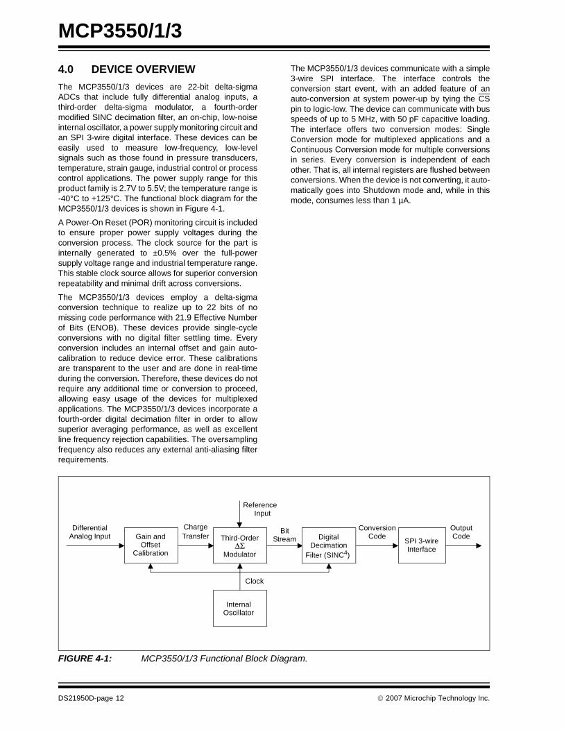
4.0 DEVICE OVERVIEW
The MCP3550/1/3 devices are 22-bit delta-sigmaADCs that include fully differential analog inputs, athird-order delta-sigma modulator, a fourth-ordermodified SINC decimation filter, an on-chip, low-noiseinternal oscillator, a power supply monitoring circuit andan SPI 3-wire digital interface. These devices can beeasily used to measure low-frequency, low-levelsignals such as those found in pressure transducers,temperature, strain gauge, industrial control or processcontrol applications. The power supply range for thisproduct family is 2.7V to 5.5V; the temperature range is-40°C to +125°C. The functional block diagram for theMCP3550/1/3 devices is shown in Figure 4-1.
A Power-On Reset (POR) monitoring circuit is includedto ensure proper power supply voltages during theconversion process. The clock source for the part isinternally generated to ±0.5% over the full-powersupply voltage range and industrial temperature range.This stable clock source allows for superior conversionrepeatability and minimal drift across conversions.
The MCP3550/1/3 devices employ a delta-sigmaconversion technique to realize up to 22 bits of nomissing code performance with 21.9 Effective Numberof Bits (ENOB). These devices provide single-cycleconversions with no digital filter settling time. Everyconversion includes an internal offset and gain auto-calibration to reduce device error. These calibrationsare transparent to the user and are done in real-timeduring the conversion. Therefore, these devices do notrequire any additional time or conversion to proceed,allowing easy usage of the devices for multiplexedapplications. The MCP3550/1/3 devices incorporate afourth-order digital decimation filter in order to allowsuperior averaging performance, as well as excellentline frequency rejection capabilities. The oversamplingfrequency also reduces any external anti-aliasing filterrequirements.
The MCP3550/1/3 devices communicate with a simple3-wire SPI interface. The interface controls theconversion start event, with an added feature of anauto-conversion at system power-up by tying the CSpin to logic-low. The device can communicate with busspeeds of up to 5 MHz, with 50 pF capacitive loading.The interface offers two conversion modes: SingleConversion mode for multiplexed applications and aContinuous Conversion mode for multiple conversionsin series. Every conversion is independent of eachother. That is, all internal registers are flushed betweenconversions. When the device is not converting, it auto-matically goes into Shutdown mode and, while in thismode, consumes less than 1 µA.
FIGURE 4-1: MCP3550/1/3 Functional Block Diagram.
InternalOscillator
Third-OrderΔΣ
Modulator
DigitalDecimation
Filter (SINC4)
SPI 3-wireInterface
Gain andOffset
Calibration
DifferentialAnalog Input
Bit ConversionCode
OutputCode
Clock
ChargeTransfer
ReferenceInput
Stream
DS21950D-page 12 © 2007 Microchip Technology Inc.

MCP3550/1/3
4.1 MCP3550/1/3 Delta-Sigma Modulator with Internal Offset and Gain Calibration
The converter core of the MCP3550/1/3 devices is athird-order delta-sigma modulator with automatic gainand offset error calibrations. The modulator uses a 1-bitDAC structure. The delta-sigma modulator processesthe sampled charges through switched capacitorstructures controlled by a very low drift oscillator forreduced clock jitter.
During the conversion process, the modulator outputsa bit stream with the bit frequency equivalent to thefOSC/4 (see Table 4-1). The high oversamplingimplemented in the modulator ensures very highresolution and high averaging factor to achieve low-noise specifications. The bit stream output of the mod-ulator is then processed by the digital decimation filterin order to provide a 22-bit output code at a data rate of12.5 Hz for the MCP3550-50, 15 Hz for the MCP3550-60, 13.75 Hz for the MCP3551 and 60 Hz for theMCP3553. Since the oversampling ratio is lower withthe MCP3553 device, a much higher output data rate isachieved while still achieving 20 bits No Missing Codes(NMC) and 20.6 ENOB.
A self-calibration of offset and gain occurs at the onsetof every conversion. The conversion data available atthe output of the device is always calibrated for offsetand gain through this process. This offset and gainauto-calibration is performed internally and has noimpact on the speed of the converter since the offsetand gain errors are calibrated in real-time during theconversion. The real-time offset and gain calibrationschemes do not affect the conversion process.
4.2 Digital Filter
The MCP3550/1/3 devices include a digital decimationfilter, which is a fourth-order modified SINC filter. Thisfilter averages the incoming bit stream from the modu-lator and outputs a 22-bit conversion word in binarytwo's complement. When all bits have been processedby the filter, the output code is ready for SPI communi-cation, the RDY flag is set on the SDO/RDY pin and allthe internal registers are reset in order to process thenext conversion.
Like the commonly used SINC filter, the modified SINCfilter in the MCP3550/1/3 family has the main notchfrequency located at fS/(OSR*L), where fS is the bitstream sample frequency. OSR is the OversamplingRatio and L is the order of the filter.
The MCP3550-50 device has the main filter notchlocated at 50 Hz. For the MCP3550-60 device, thenotch is located at 60 Hz. The MCP3551 device has itsnotch located at 55 Hz, and for the MCP3553 device,the main notch is located at 240 Hz, with an OSR of128. (see Table 4-1 for rejection performance).
The digital decimation SINC filter has been modified inorder to offer staggered zeros in its transfer function.This modification is intended to widen the main notch inorder to be less sensitive to oscillator deviation or line-frequency drift. The MCP3551 filter has staggeredzeros spread in order to reject both 50 Hz and 60 Hzline frequencies simultaneously (see Figure 4-2).
TABLE 4-1: DATA RATE, OUTPUT NOISE AND DIGITAL FILTER SPECIFICATIONS BY DEVICE
DeviceOutput Data Rate (tCONV)
(Note)
Output Noise
(µVRMS)
Primary Notch(Hz)
Sample Frequency
(fS)
Internal Clock fOSC
50/60 Hz Rejection
MCP3550-50 80.00 ms 2.5 50 25600 Hz 102.4 kHz -120 dB min. at 50 Hz
MCP3550-60 66.67 ms 2.5 60 30720 Hz 122.88 kHz -120 dB min. at 60 Hz
MCP3551 72.73 ms 2.5 55 28160 Hz 112.64 kHz -82 dB min. from 48 Hz to 63 Hz. -
82 dB at 50 Hz and -88 dB at 60 Hz
MCP3553 16.67 ms 6 240 30720 Hz 122.88 kHz Not Applicable
Note: For the first conversion after exiting Shutdown, tCONV must include an additional 144 fOSC periods beforethe conversion is complete and the RDY (Ready) flag appears on SDO/RDY.
© 2007 Microchip Technology Inc. DS21950D-page 13

MCP3550/1/3
:FIGURE 4-2: SINC Filter Response, MCP3550-50 Device.:
FIGURE 4-3: SINC Filter Response, MCP3550-60 Device.:
FIGURE 4-4: SINC Filter Response, MCP3551 Device, Simultaneous 50/60 Hz Rejection.
FIGURE 4-5: SINC Filter Response at Integer Multiples of the Sampling Frequency (fs).
4.3 Internal Oscillator
The MCP3550/1/3 devices include a highly stable andaccurate internal oscillator that provides clock signalsto the delta-sigma ADC with minimum jitter. The oscil-lator is a specialized structure with a low temperaturecoefficient across the full range of specified operation.See Table 4-1 for oscillator frequencies.
The conversion time is an integer multiple of the inter-nal clock period and, therefore, has the same accuracyas the internal clock frequency. The internal oscillatorfrequency is 102.4 kHz ±1% for the MCP3550-50,112.64 kHz ±1% for the MCP3551, and 122.88 kHz±1% for the MCP3550-60 and MCP3553 devices,across the full power supply voltage and specifiedtemperature ranges.
The notch of the digital filter is proportional to theinternal oscillator frequency, with the exact notchfrequency equivalent to the oscillator accuracy (< 1%deviation). This high accuracy, combined with widenotches, will ensure that the MCP3551 will have simul-taneous 50 Hz and 60 Hz line frequency rejection andthe MCP3550-50 or MCP3550-60 devices will havegreater than 120 dB rejection (at either 50 or 60 Hz) bythe digital filtering, even when jitter is present.
The internal oscillator is held in the reset conditionwhen the part is in Shutdown mode to ensure very lowpower consumption (< 1 µA in Shutdown mode). Theinternal oscillator is independent of all serial digitalinterface edges (i.e., state machine processing thedigital SPI interface is asynchronous with respect to theinternal clock edges).
-120
-100
-80
-60
-40
-20
0
0 50 100 150 200
Frequency (Hz)
Att
enu
atio
n (
dB
)
-120
-100
-80
-60
-40
-20
0
0 60 120 180 240
Frequency (Hz)
Att
enu
atio
n (
dB
)
-120-110-100
-90-80-70-60-50-40-30-20-10
0
0 10 20 30 40 50 60 70 80 90 100 110
Frequency (Hz)
Att
enu
atio
n (
dB
)
-140
-120
-100
-80
-60
-40
-20
0
0 28160 56320 84480 112640 140800 168960 197120 225280 253440
Frequency (Hz)
No
rmal
Mo
de
Rej
ecti
on
(d
B)
DS21950D-page 14 © 2007 Microchip Technology Inc.

MCP3550/1/3
4.4 Differential Analog InputsThe MCP3550/1/3 devices accept a fully differentialanalog input voltage to be connected to the VIN+ andVIN- input pins. The differential voltage that is convertedis defined by VIN = VIN+ – VIN-. The differential voltagerange specified for ensured accuracy is from -VREF to+VREF.
The converter will output valid and usable codes from -112% to 112% of output range (see Section 5.0“Serial Interface”) at room temperature. The ±12%overrange is clearly specified by two overload bits inthe output code: OVH and OVL. This feature allows forsystem calibration of a positive gain error.
The absolute voltage range on these input pins extendsfrom VSS - 0.3V to VDD + 0.3V. If the input voltages areabove or below this range, the leakage currents of theESD diodes will increase exponentially, degrading theaccuracy and noise performance of the converter. Thecommon mode of the analog inputs should be chosensuch that both the differential analog input range andabsolute voltage range on each pin are within thespecified operating range defined in Section 1.0“Electrical Characteristics”.
Both the analog differential inputs and the referenceinput have switched-capacitor input structures. Theinput capacitors are charged and discharged alterna-tively with the input and the reference in order toprocess a conversion. The charge and discharge of theinput capacitors create dynamic input currents at theVIN+ and VIN- input pins inversely proportional to thesampling capacitor. This current is a function of thedifferential input voltages and their respective commonmodes. The typical value of the differential input imped-ance is 2.4 MΩ, with VCM = 2.5V, VDD = VREF = 5V. TheDC leakage current caused by the ESD input diodes,even though on the order of 1 nA, can cause additionaloffset errors proportional to the source resistance at theVIN+ and VIN- input pins.
From a transient response standpoint and as a first-order approximation, these input structures form asimple RC filtering circuit with the source impedance inseries with the RON (switched resistance when closed)of the input switch and the sampling capacitor. In orderto ensure the accuracy of the sampled charge, propersettling time of the input circuit has to be considered.Slow settling of the input circuit will create additionalgain error. As a rule of thumb, in order to obtain 1 ppmabsolute measurement accuracy, the sampling periodmust be 14 times greater than the input circuit RC timeconstant.
4.5 Voltage Reference Input Pin
The MCP3550/1/3 devices accept a single-endedexternal reference voltage, to be connected on theVREF input pin. Internally, the reference voltage for theADC is a differential voltage with the non-inverting inputconnected to the VREF pin and the inverting inputconnected to the VSS pin. The value of the referencevoltage is VREF - VSS and the common mode of thereference is always (VREF - VSS)/2.
The MCP3550/1/3 devices accept a single-endedreference voltage from 0.1V to VDD. The converteroutput noise is dominated by thermal noise that isindependent of the reference voltage. Therefore, theoutput noise is not significantly improved by loweringthe reference voltage at the VREF input pin. However, areduced reference voltage will significantly improve theINL performance since the INL max error isproportional to VREF
2 (see Figure 2-4).
The charge and discharge of the input capacitor createdynamic input currents at the VREF input pin inverselyproportional to the sampling capacitor, which is a func-tion of the input reference voltage. The typical value ofthe single-ended input impedance is 2.4 MΩ, withVDD = VREF = 5V. The DC leakage current caused bythe ESD input diodes, though on the order of 1 nAtypically, can cause additional gain error proportional tothe source resistance at the VREF pin.
4.6 Power-On Reset (POR)
The MCP3550/1/3 devices contain an internal Power-On Reset (POR) circuit that monitors power supplyvoltage VDD during operation. This circuit ensurescorrect device start-up at system power-up and power-down events. The POR has built-in hysteresis and atimer to give a high degree of immunity to potentialripple and noise on the power supplies, as well as toallow proper settling of the power supply during power-up. A 0.1 µF decoupling capacitor should be mountedas close as possible to the VDD pin, providing additionaltransient immunity.
The threshold voltage is set at 2.2V, with a tolerance ofapproximately ±5%. If the supply voltage falls belowthis threshold, the MCP3550/1/3 devices will be held ina reset condition or in Shutdown mode. When the partis in Shutdown mode, the power consumption is lessthan 1 µA. The typical hysteresis value is around200 mV in order to prevent reset during brown-out orother glitches on the power supply.
© 2007 Microchip Technology Inc. DS21950D-page 15

MCP3550/1/3
Once a power-up event has occurred, the device mustrequire additional time before a conversion can takeplace. During this time, all internal analog circuitry mustsettle before the first conversion can occur. An internaltimer counts 32 internal clock periods before theinternal oscillator can provide clock to the conversionprocess. This allows all internal analog circuitry tosettle to their proper operating point. This timing istypically less than 300 µs, which is negligible comparedto one conversion time (e.g. 72.7 ms for theMCP3551). Figure 4-6 illustrates the conditions for apower-up and power-down event under typical start-upconditions.
FIGURE 4-6: Power-On Reset Operation.
4.7 Shutdown Mode
When not internally converting, the two modes ofoperation for the MCP3550/1/3 devices are theShutdown and Sleep modes. During Shutdown mode,all internal analog circuitry, including the POR, is turnedoff and the device consumes less than 1 µA. Whenexiting Shutdown mode, the device must require addi-tional time before a conversion can take place. Duringthis time, all internal analog circuitry must settle beforethe first conversion can occur. An internal timer counts32 internal clock periods before the internal oscillatorcan provide clock to the conversion process. Thisallows all internal analog circuitry to settle to theirproper operating point. This timing is typically less than300 µs, which is negligible compared to one conversiontime (72.7 ms for MCP3551).
4.8 Sleep Mode
During Sleep mode, the device is not converting and isawaiting data retrieval; the internal analog circuitry isstill running and the device typically consumes 10 µA.In order to restart a conversion while in Sleep mode,toggling CS to a logic-high (placing the part in Shut-down mode) and then back to a logic-low will restart theconversion. Sleep can only be entered in SingleConversion mode. Once a conversion is complete inSingle Conversion mode, the device automaticallyenters Sleep mode.
VDD
2.2V2.0V
0V
ResetNormal
Operation ResetStart-up
Time
300 µs
DS21950D-page 16 © 2007 Microchip Technology Inc.

MCP3550/1/3
5.0 SERIAL INTERFACE
5.1 Overview
Serial communication between the microcontroller andthe MCP3550/1/3 devices is achieved using CS, SCKand SDO/RDY. There are two modes of operation:Single Conversion and Continuous Conversion. CScontrols the conversion start. There are 24 bits in thedata word: 22 bits of conversion data and two overflowbits. The conversion process takes place via the inter-nal oscillator and the status of this conversion must bedetected. The typical method of communication isshown in Figure 5-1. The status of the internal conver-sion is the SDO/RDY pin and is available with CS low.A High state on SDO/RDY means the device is busyconverting, while a Low state means the conversion isfinished and data is ready for transfer using SCK.SDO/RDY remains in a high-impedance state whenCS is held high. CS must be low when clocking out thedata using SCK and SDO/RDY.
Bit 22 is Overflow High (OVH) when VIN > VREF – 1 LSB,OVH toggles to logic ‘1’, detecting an overflow high inthe analog input voltage.
Bit 23 is Overflow Low (OVL) when VIN < -VREF, OVLtoggles to logic ‘1’, detecting an overflow low in theanalog input voltage. The state OVH = OVL = ‘1’ is notdefined and should be considered as an interrupt forthe SPI interface meaning erroneous communication.
Bit 21 to bit 0 represents the output code in 22-bitbinary two's complement. Bit 21 is the sign bit and islogic ‘0’ when the differential analog input is positiveand logic ‘1’ when the differential analog input isnegative. From Bit 20 to bit 0, the output code is givenMSb first (MSb is bit 20 and LSB is Bit 0). When theanalog input value is comprised between -VREF andVREF – 1 LSB, the two overflow bits are set to logic ‘0’.The relationship between input voltage and outputcode is shown in Figure 5-1.
The delta-sigma modulator saturation point for thedifferential analog input is located at around ±112% ofVREF (at room temperature), meaning that the modula-tor will still give accurate output codes with an over-range of 12% below or above the reference voltage.Unlike the usual 22-bit device, the 22-bit output codewill not lock at 0x1FFFFF for positive sign inputs or0x200000 for negative sign inputs in order to takeadvantage of the overrange capabilities of the device.This can be practical for closed-loop operations, forinstance. In case of an overflow, the output codebecomes a 23-bit two's complement output code,where the sign bit will be the OVL bit. If an overflow highor low is detected, OVL (bit 23) becomes the sign bit(instead of bit 21), the MSb is then bit 21 and the con-verter can be used as a 23-bit two's complement codeconverter, with output code from bits B21 to B0, andOVL as the sign bit. Figure 5-1 summarizes the outputcoding data format with or without overflow high andlow.
FIGURE 5-1: Typical Serial Device Communication and Example Digital Output Codes for Specific Analog Input Voltages.
CS
SCK
D O O21 20 19 18 17 16 15 14 13 12 11 10 9 8 7 6 5 4 3 2 1 0
READY HLRHI-ZSDO/RDY
© 2007 Microchip Technology Inc. DS21950D-page 17

MCP3550/1/3
5.2 Controlling Internal Conversions and the Internal Oscillator
During Shutdown mode, on the falling edge of CS, theconversion process begins. During this process, theinternal oscillator clocks the delta-sigma modulator andthe SINC filter until a conversion is complete. Thisconversion time is tCONV and the timing is shown inFigure 5-2. At the end of tCONV, the digital filter hassettled completely and there is no latency involved withthe digital SINC filter of the MCP3550/1/3.
The two modes of conversion for the MCP3550/1/3devices are Single Conversion and ContinuousConversion. In Single Conversion mode, a consecutiveconversion will not automatically begin. Instead, after asingle conversion is complete and all four filters havesettled, the device puts the data into the output registerand enters shutdown.
In Continuous Conversion mode, a consecutiveconversion will be automatic. In this mode, the deviceis continuously converting, independent of the serialinterface. The most recent conversion data will alwaysbe available in the Output register.
When the device exits Shutdown, there is an internalpower-up delay that must be observed.
FIGURE 5-2: Single Conversion Mode.
FIGURE 5-3: Continuous Conversion Mode.
CS
Int. Osc
tCONV Sleep Shutdown
SCK (opt)
SDO/RDY Hi-Z Hi-Z
x24
CS
Int. Osc
tCONV
Shutdown
SCK (opt)
tCONV tCONV
SDO/RDY Hi-Z
x24
DS21950D-page 18 © 2007 Microchip Technology Inc.

MCP3550/1/3
5.3 Single Conversion Mode
If a rising edge of Chip Select (CS) occurs during tCONV,a subsequent conversion will not take place and thedevice will enter low-power Shutdown mode aftertCONV completes. This is referred to as SingleConversion mode. This operation is demonstrated inFigure 5-3. Note that a falling edge of CS during thesame conversion that detected a rising edge, as inFigure 5-2, will not initiate a new conversion. Once arising edge is seen, the device will enter Sleep, thenShutdown mode. Once the device has been put intoSingle Conversion mode, the data must be clocked outin order for a new conversion to take place. Asubsequent falling edge on CS during Shutdown modewill not initiate a new conversion, unless the priorconversion data has been clocked out of the device.After the final data bit has been clocked out on the 25thclock, the SDO/RDY pin will go active-high.
5.3.1 READY FUNCTION OF SDO/RDY PIN, SINGLE CONVERSION MODE
At every falling edge of CS during the internal conver-sion, the state of the internal conversion is latched onthe SDO/RDY pin to give ready or busy information. AHigh state means the device is currently performing aninternal conversion and data cannot be clocked out. ALow state means the device has finished its conversionand the data is ready for retrieval on the falling edge ofSCK. This operation is demonstrated in Figure 5-4.Note that the device has been put into SingleConversion mode with the first rising edge of CS.
FIGURE 5-4: RDY Functionality in Single Conversion Mode.
5.4 Continuous Conversion Mode
If no rising edge of CS occurs during any given conver-sion per Figure 5-2, a subsequent conversion will takeplace and the contents of the previous conversion willbe overwritten. This operation is demonstrated inFigure 5-5. Once conversion output data has started tobe clocked out, the output buffer is not refreshed untilall 24 bits have been clocked. A complete read mustoccur in order to read the next conversion in this mode.The subsequent conversion data to be read will then bethe most recent conversion. The conversion time isfixed and cannot be shortened by the rising edge of CS.This rising edge will place the part in Shutdown modeand all conversion data will be lost.
The transfer of data from the SINC filter to the outputbuffer is demonstrated in Figure 5-5. If the previousconversion data is not clocked out of the device, it willbe lost and replaced by the new conversion. When thedevice is in Continuous Conversion mode, the mostrecent conversion data is always present at the outputregister for data retrieval.
FIGURE 5-5: Most Current Continuous Conversion Mode Data.
If a conversion is in process, it cannot be terminatedwith the rising edge of CS. SDO/RDY must firsttransition to a Low state, which will indicate the end ofconversion.
5.4.1 READY FUNCTION OF SDO/RDY PIN IN CONTINUOUS CONVERSION MODE
The device enters Continuous Conversion mode if norising edge of CS is seen during tCONV and consecu-tive conversions ensue. SDO/RDY will be high,indicating that a conversion is in process. When aconversion is complete, SDO/RDY will change to aLow state. With the Low state of SDO/RDY after thisfirst conversion, the conversion data can be accessedwith the combination of SCK and SDO/RDY. If the dataready event happens during the clocking out of thedata, the data ready bit will be displayed after thecomplete 24-bit word communication (i.e., the dataready event will not interrupt a data transfer).
Note: The Ready state is latched on each fallingedge of CS and will not dynamicallyupdate if CS is held low. CS must betoggled high through low.
tCONV
CS
Int. Osc
SDO/RDYHi-Z
tCONVtCONV tCONV
CS
Int. Osc
SCK & SDO/RDY
A B C
Conversion B data is clockedout of the device here.
© 2007 Microchip Technology Inc. DS21950D-page 19

MCP3550/1/3
If 24 bits of data are required from this conversion, theymust be accessed during this communication. You canterminate data transition by bringing CS high, but theremaining data will be lost and the converter will go intoShutdown mode. Once the data has been transmittedby the converter, the SDO/RDY pin will remain in theLSB state until the 25th falling edge of SCK. At thispoint, SDO/RDY is released from the Data Acquisitionmode and changed to the RDY state.
5.4.2 2-WIRE CONTINUOUS CONVERSION OPERATION, (CS TIED PERMANENTLY LOW)
It is possible to use only two wires to communicate withthe MCP3550/1/3 devices. In this state, the device isalways in Continuous Conversion mode, with internalconversions continuously occurring. This mode can beentered by having CS low during power-up or changingit to a low position after power-up. If CS is low at power-up, the first conversion of the converter is initiatedapproximately 300 µs after the power supply hasstabilized.
Note: The RDY state is not latched to CS in thismode; the RDY flag dynamically updateson the SDO/RDY pin and remains in thisstate until data is clocked out using theSCK pin.
DS21950D-page 20 © 2007 Microchip Technology Inc.

MCP3550/1/3
5.5 Using The MCP3550/1/3 with Microcontroller (MCU) SPI Ports
It is required that the microcontroller SPI port be config-ured to clock out data on the falling edge of clock andlatch data in on the rising edge. Figure 5-6 depicts theoperation shown in SPI mode 1,1, which requires thatthe SCK from the MCU idles in the High state, whileFigure 5-7 shows the similar case of SPI Mode 0,0,where the clock idles in the Low state. The waveformsin the figures are examples of an MCU operating theSPI port in 8-bit mode, and the MCP3550/1/3 devicesdo not require data in 8-bit groups.
In SPI mode 1,1, data is read using only 24 clocks orthree byte transfers. The data ready bit must be readby testing the SDO/RDY line prior to a falling edge ofthe clock.
In SPI mode 0,0, data is read using 25 clocks or fourbyte transfers. Please note that the data ready bit isincluded in the transfer as the first bit in this mode.
FIGURE 5-6: SPI Communication – Mode 1,1.
FIGURE 5-7: SPI Communication – Mode 0,0.
CS
SCK
SDO/RDY
MCU
Data stored into MCU receiveregister after transmission offirst byte
Receive Buffer
Data stored into MCU receiveregister after transmission ofsecond byte
Data stored into MCU receiveregister after transmission ofthird byte
D O O 21 20 19 18 17 16 15 14 13 12 11 10 9 8 7 6 5 4 3 2 1 0
OL OH 21 20 19 18 17 16 15 14 13 12 11 10 9 8 7 6 5 4 3 2 1 0
R H L
CS
SCK
SDO/RDY
MCU
Data stored into MCU receiveregister after transmission offirst byte
Receive Buffer
Data stored into MCU receiveregister after transmission ofsecond byte
Data stored into MCU receiveregister after transmission ofthird byte
Data stored into MCU receiveregister after transmission offourth byte
DR O O 21 20 19 18 17 16 14 13 12 11 10 9 6 5 4 3 2 0
OH OL 21 20 19 18 17 15 14 13 12 11 10 9 7 6 5 4 3 2 1 0DR
8
16
15 7
8
1H L
© 2007 Microchip Technology Inc. DS21950D-page 21

MCP3550/1/3
6.0 PACKAGING INFORMATION
6.1 Package Marking Information
Legend: XX...X Customer-specific informationY Year code (last digit of calendar year)YY Year code (last 2 digits of calendar year)WW Week code (week of January 1 is week ‘01’)NNN Alphanumeric traceability code Pb-free JEDEC designator for Matte Tin (Sn)* This package is Pb-free. The Pb-free JEDEC designator ( )
can be found on the outer packaging for this package.
Note: In the event the full Microchip part number cannot be marked on one line, it willbe carried over to the next line, thus limiting the number of availablecharacters for customer-specific information.
3e
3e
8-Lead SOIC (150 mil) Examples:
XXXXXXXXXXXXYYWW
NNN
MCP3551ESN^^ 0715
256
8-Lead MSOP Example:
XXXXXX
YWWNNN
3553E
715256
3e
3e
DS21950D-page 22 © 2007 Microchip Technology Inc.

MCP3550/1/3
8-Lead Plastic Micro Small Outline Package (MS) [MSOP]
Notes:1. Pin 1 visual index feature may vary, but must be located within the hatched area.2. Dimensions D and E1 do not include mold flash or protrusions. Mold flash or protrusions shall not exceed 0.15 mm per side.3. Dimensioning and tolerancing per ASME Y14.5M.
BSC: Basic Dimension. Theoretically exact value shown without tolerances.REF: Reference Dimension, usually without tolerance, for information purposes only.
Note: For the most current package drawings, please see the Microchip Packaging Specification located at http://www.microchip.com/packaging
Units MILLIMETERS
Dimension Limits MIN NOM MAX
Number of Pins N 8
Pitch e 0.65 BSC
Overall Height A – – 1.10
Molded Package Thickness A2 0.75 0.85 0.95
Standoff A1 0.00 – 0.15
Overall Width E 4.90 BSC
Molded Package Width E1 3.00 BSC
Overall Length D 3.00 BSC
Foot Length L 0.40 0.60 0.80
Footprint L1 0.95 REF
Foot Angle φ 0° – 8°
Lead Thickness c 0.08 – 0.23
Lead Width b 0.22 – 0.40
D
N
E
E1
NOTE 1
1 2
e
b
A
A1
A2c
L1 L
φ
Microchip Technology Drawing C04-111B
© 2007 Microchip Technology Inc. DS21950D-page 23
MCP3550/1/3
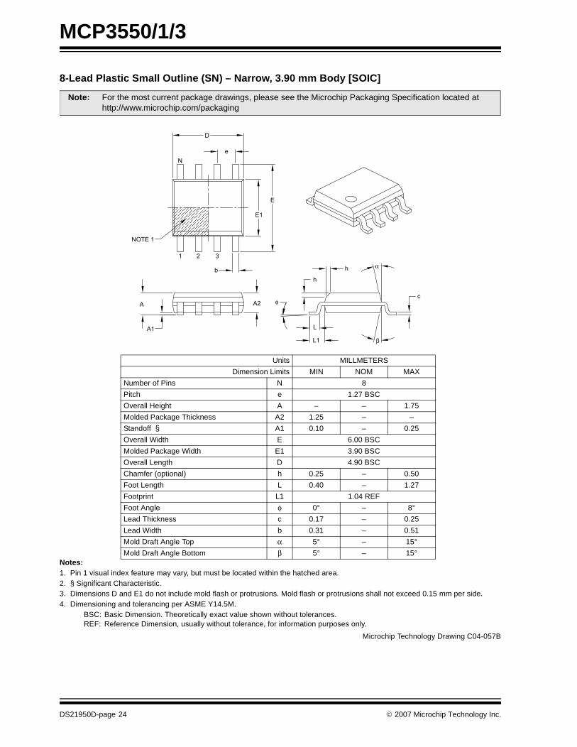
8-Lead Plastic Small Outline (SN) – Narrow, 3.90 mm Body [SOIC]
Notes:1. Pin 1 visual index feature may vary, but must be located within the hatched area.2. § Significant Characteristic.3. Dimensions D and E1 do not include mold flash or protrusions. Mold flash or protrusions shall not exceed 0.15 mm per side.4. Dimensioning and tolerancing per ASME Y14.5M.
BSC: Basic Dimension. Theoretically exact value shown without tolerances.REF: Reference Dimension, usually without tolerance, for information purposes only.
Note: For the most current package drawings, please see the Microchip Packaging Specification located at http://www.microchip.com/packaging
Units MILLMETERS
Dimension Limits MIN NOM MAX
Number of Pins N 8
Pitch e 1.27 BSC
Overall Height A – – 1.75
Molded Package Thickness A2 1.25 – –
Standoff § A1 0.10 – 0.25
Overall Width E 6.00 BSC
Molded Package Width E1 3.90 BSC
Overall Length D 4.90 BSC
Chamfer (optional) h 0.25 – 0.50
Foot Length L 0.40 – 1.27
Footprint L1 1.04 REF
Foot Angle φ 0° – 8°
Lead Thickness c 0.17 – 0.25
Lead Width b 0.31 – 0.51
Mold Draft Angle Top α 5° – 15°
Mold Draft Angle Bottom β 5° – 15°
D
N
e
E
E1
NOTE 1
1 2 3
b
A
A1
A2
L
L1
c
h
h
φ
β
α
Microchip Technology Drawing C04-057B
DS21950D-page 24 © 2007 Microchip Technology Inc.

MCP3550/1/3
APPENDIX A: REVISION HISTORY
Revision A (September 2005)
• Original Release of this Document.
Revision B (October 2005)
• Changed LSb refefences to LSB.
Revision C (December 2005)• Added MCP3550-50, MCP3550-60 references
throughout this document.
Revision D (January 2007)
• This update includes revisions to the packaging diagrams.
© 2007 Microchip Technology Inc. DS21950D-page 25

MCP3550/1/3
NOTES:
DS21950D-page 26 © 2007 Microchip Technology Inc.

MCP3550/1/3
PRODUCT IDENTIFICATION SYSTEM
To order or obtain information, e.g., on pricing or delivery, refer to the factory or the listed sales office.
Device: MCP3550-50: Single Channel 22-Bit Delta-Sigma ADCMCP3550T-50: Single Channel 22-Bit Delta-Sigma ADC
(Tape and Reel)MCP3550-60: Single Channel 22-Bit Delta-Sigma ADCMCP3550T-60: Single Channel 22-Bit Delta-Sigma ADC
(Tape and Reel)MCP3551: Single Channel 22-Bit Delta-Sigma ADCMCP3551T: Single Channel 22-Bit Delta-Sigma ADC
(Tape and Reel)MCP3553: Single Channel 22-Bit Delta-Sigma ADCMCP3553T: Single Channel 22-Bit Delta-Sigma ADC
(Tape and Reel)
Temperature Range: E = -40°C to +125°C
Package: MS = Plastic MSOP, 8-leadSN = Plastic SOIC (150 mil Body), 8-lead
PART NO. –X /XX
PackageTemperatureRange
Device
Examples:
a) MCP3550-50-E/MS: Extended Temp., 8LD MSOP.
b) MCP3550/1T-50E/MS:Tape and Reel,Extended Temp.,8LD MSOP.
c) MCP3550-60-E/SN: Extended Temp.,8LD SOIC.
d) MCP3550/1T-60E/SN:Tape and Reel,Extended Temp.,8LD SOIC.
a) MCP3551-E/MS: Extended Temp., 8LD MSOP.
b) MCP3551T-E/MS: Tape and Reel,Extended Temp.,8LD MSOP.
c) MCP3553-E/SN: Extended Temp.,8LD SOIC.
d) MCP3553T-E/SN: Tape and Reel,Extended Temp.,8LD SOIC.
© 2007 Microchip Technology Inc. DS21950D-page 27

MCP3550/1/3
NOTES:
DS21950D-page 28 © 2007 Microchip Technology Inc.

Note the following details of the code protection feature on Microchip devices:
• Microchip products meet the specification contained in their particular Microchip Data Sheet.
• Microchip believes that its family of products is one of the most secure families of its kind on the market today, when used in the intended manner and under normal conditions.
• There are dishonest and possibly illegal methods used to breach the code protection feature. All of these methods, to our knowledge, require using the Microchip products in a manner outside the operating specifications contained in Microchip’s Data Sheets. Most likely, the person doing so is engaged in theft of intellectual property.
• Microchip is willing to work with the customer who is concerned about the integrity of their code.
• Neither Microchip nor any other semiconductor manufacturer can guarantee the security of their code. Code protection does not mean that we are guaranteeing the product as “unbreakable.”
Code protection is constantly evolving. We at Microchip are committed to continuously improving the code protection features of ourproducts. Attempts to break Microchip’s code protection feature may be a violation of the Digital Millennium Copyright Act. If such actsallow unauthorized access to your software or other copyrighted work, you may have a right to sue for relief under that Act.
Information contained in this publication regarding deviceapplications and the like is provided only for your convenienceand may be superseded by updates. It is your responsibility toensure that your application meets with your specifications.MICROCHIP MAKES NO REPRESENTATIONS ORWARRANTIES OF ANY KIND WHETHER EXPRESS ORIMPLIED, WRITTEN OR ORAL, STATUTORY OROTHERWISE, RELATED TO THE INFORMATION,INCLUDING BUT NOT LIMITED TO ITS CONDITION,QUALITY, PERFORMANCE, MERCHANTABILITY ORFITNESS FOR PURPOSE. Microchip disclaims all liabilityarising from this information and its use. Use of Microchipdevices in life support and/or safety applications is entirely atthe buyer’s risk, and the buyer agrees to defend, indemnify andhold harmless Microchip from any and all damages, claims,suits, or expenses resulting from such use. No licenses areconveyed, implicitly or otherwise, under any Microchipintellectual property rights.
© 2007 Microchip Technology Inc.
Trademarks
The Microchip name and logo, the Microchip logo, Accuron, dsPIC, KEELOQ, microID, MPLAB, PIC, PICmicro, PICSTART, PRO MATE, PowerSmart, rfPIC, and SmartShunt are registered trademarks of Microchip Technology Incorporated in the U.S.A. and other countries.
AmpLab, FilterLab, Migratable Memory, MXDEV, MXLAB, SEEVAL, SmartSensor and The Embedded Control Solutions Company are registered trademarks of Microchip Technology Incorporated in the U.S.A.
Analog-for-the-Digital Age, Application Maestro, CodeGuard, dsPICDEM, dsPICDEM.net, dsPICworks, ECAN, ECONOMONITOR, FanSense, FlexROM, fuzzyLAB, In-Circuit Serial Programming, ICSP, ICEPIC, Linear Active Thermistor, Mindi, MiWi, MPASM, MPLIB, MPLINK, PICkit, PICDEM, PICDEM.net, PICLAB, PICtail, PowerCal, PowerInfo, PowerMate, PowerTool, REAL ICE, rfLAB, rfPICDEM, Select Mode, Smart Serial, SmartTel, Total Endurance, UNI/O, WiperLock and ZENA are trademarks of Microchip Technology Incorporated in the U.S.A. and other countries.
SQTP is a service mark of Microchip Technology Incorporated in the U.S.A.
All other trademarks mentioned herein are property of their respective companies.
© 2007, Microchip Technology Incorporated, Printed in the U.S.A., All Rights Reserved.
Printed on recycled paper.
DS21950D-page 29
Microchip received ISO/TS-16949:2002 certification for its worldwide headquarters, design and wafer fabrication facilities in Chandler and Tempe, Arizona, Gresham, Oregon and Mountain View, California. The Company’s quality system processes and procedures are for its PIC®
MCUs and dsPIC DSCs, KEELOQ® code hopping devices, Serial EEPROMs, microperipherals, nonvolatile memory and analog products. In addition, Microchip’s quality system for the design and manufacture of development systems is ISO 9001:2000 certified.

DS21950D-page 30 © 2007 Microchip Technology Inc.
AMERICASCorporate Office2355 West Chandler Blvd.Chandler, AZ 85224-6199Tel: 480-792-7200 Fax: 480-792-7277Technical Support: http://support.microchip.comWeb Address: www.microchip.com
AtlantaDuluth, GA Tel: 678-957-9614 Fax: 678-957-1455
BostonWestborough, MA Tel: 774-760-0087 Fax: 774-760-0088
ChicagoItasca, IL Tel: 630-285-0071 Fax: 630-285-0075
DallasAddison, TX Tel: 972-818-7423 Fax: 972-818-2924
DetroitFarmington Hills, MI Tel: 248-538-2250Fax: 248-538-2260
KokomoKokomo, IN Tel: 765-864-8360Fax: 765-864-8387
Los AngelesMission Viejo, CA Tel: 949-462-9523 Fax: 949-462-9608
Santa ClaraSanta Clara, CA Tel: 408-961-6444Fax: 408-961-6445
TorontoMississauga, Ontario, CanadaTel: 905-673-0699 Fax: 905-673-6509
ASIA/PACIFICAsia Pacific OfficeSuites 3707-14, 37th FloorTower 6, The GatewayHabour City, KowloonHong KongTel: 852-2401-1200Fax: 852-2401-3431
Australia - SydneyTel: 61-2-9868-6733Fax: 61-2-9868-6755
China - BeijingTel: 86-10-8528-2100 Fax: 86-10-8528-2104
China - ChengduTel: 86-28-8665-5511Fax: 86-28-8665-7889
China - FuzhouTel: 86-591-8750-3506 Fax: 86-591-8750-3521
China - Hong Kong SARTel: 852-2401-1200 Fax: 852-2401-3431
China - QingdaoTel: 86-532-8502-7355Fax: 86-532-8502-7205
China - ShanghaiTel: 86-21-5407-5533 Fax: 86-21-5407-5066
China - ShenyangTel: 86-24-2334-2829Fax: 86-24-2334-2393
China - ShenzhenTel: 86-755-8203-2660 Fax: 86-755-8203-1760
China - ShundeTel: 86-757-2839-5507 Fax: 86-757-2839-5571
China - WuhanTel: 86-27-5980-5300Fax: 86-27-5980-5118
China - XianTel: 86-29-8833-7250Fax: 86-29-8833-7256
ASIA/PACIFICIndia - BangaloreTel: 91-80-4182-8400 Fax: 91-80-4182-8422
India - New DelhiTel: 91-11-4160-8631Fax: 91-11-4160-8632
India - PuneTel: 91-20-2566-1512Fax: 91-20-2566-1513
Japan - YokohamaTel: 81-45-471- 6166 Fax: 81-45-471-6122
Korea - GumiTel: 82-54-473-4301Fax: 82-54-473-4302
Korea - SeoulTel: 82-2-554-7200Fax: 82-2-558-5932 or 82-2-558-5934
Malaysia - PenangTel: 60-4-646-8870Fax: 60-4-646-5086
Philippines - ManilaTel: 63-2-634-9065Fax: 63-2-634-9069
SingaporeTel: 65-6334-8870Fax: 65-6334-8850
Taiwan - Hsin ChuTel: 886-3-572-9526Fax: 886-3-572-6459
Taiwan - KaohsiungTel: 886-7-536-4818Fax: 886-7-536-4803
Taiwan - TaipeiTel: 886-2-2500-6610 Fax: 886-2-2508-0102
Thailand - BangkokTel: 66-2-694-1351Fax: 66-2-694-1350
EUROPEAustria - WelsTel: 43-7242-2244-39Fax: 43-7242-2244-393Denmark - CopenhagenTel: 45-4450-2828 Fax: 45-4485-2829
France - ParisTel: 33-1-69-53-63-20 Fax: 33-1-69-30-90-79
Germany - MunichTel: 49-89-627-144-0 Fax: 49-89-627-144-44
Italy - Milan Tel: 39-0331-742611 Fax: 39-0331-466781
Netherlands - DrunenTel: 31-416-690399 Fax: 31-416-690340
Spain - MadridTel: 34-91-708-08-90Fax: 34-91-708-08-91
UK - WokinghamTel: 44-118-921-5869Fax: 44-118-921-5820
WORLDWIDE SALES AND SERVICE
12/08/06