mdbt40 & mdbt40-p - version a15
TRANSCRIPT
Version: A15
Issued Date: 2021/07/23
Approval Sheet
(產品承認書)
產品名稱 (Product) Bluetooth Low Energy Module
解決方案 (Solution) Nordic nRF51822 QFN Package
產品型號 (Model No.) MDBT40 Series (Chip Antenna)
MDBT40-P Series (PCB Antenna)
產品料號 (Part No.) see 4.3 Order Code
Advantage of MDBT40 & MDBT40-P series:
1. Long working distance under 1 Mbps:
MDBT40: over 80 meters in open space.
MDBT40-P: up to 60 meters in open space.
2. Declaration ID includes all Nordic applied profiles.
3. Granted main regional certification such as FCC (USA), CE(EU)
TELEC (Japan), SRRC (China), IC (Canada), NCC (Taiwan), KC (South Korea)
RCM (Australia & New Zealand) and ANATEL (Brazil).

Index
1. Overall Introduction ...................................................................................................... 4
1.1. Application ............................................................................................................ 4
1.2. Features ............................................................................................................... 5
2. Product Dimension ....................................................................................................... 6
2.1. PCB Dimensions & Pin Indication ......................................................................... 6
2.2. Recommended Layout of Solder Pad ................................................................... 8
2.3. RF Layout Suggestion (aka Keep-Out Area) ...................................................... 12
2.4. Footprint & Design Guide ................................................................................... 14
2.5. Pin Assignment ................................................................................................... 15
3. Main Chip Solution ...................................................................................................... 17
4. Shipment Packaging Information .............................................................................. 18
4.1. Marking on Metal Shield ..................................................................................... 19
4.2. Packaging Info .................................................................................................... 19
4.3. Order Code ......................................................................................................... 21
5. Specification ................................................................................................................ 22
5.1. Industrial Temperature Range ............................................................................ 22
5.2. Absolute Maximum Ratings ................................................................................ 23
5.3. Operation Conditions .......................................................................................... 23
5.4. Electrical Specifications ...................................................................................... 24
6. Block Diagram ............................................................................................................. 30
7. Antenna ........................................................................................................................ 31
7.1. MDBT40 Series .................................................................................................. 31
7.2. MDBT40-P Series ............................................................................................... 33
8. Reference Circuit ......................................................................................................... 34
8.1. Internal LDO Mode (Module’s Default).............................................................. 34
8.2. 1.8V Low Voltage Mode ...................................................................................... 35
8.3. Internal DC/DC Converter Mode ......................................................................... 36
9. Certification ................................................................................................................. 37
9.1. Declaration ID ..................................................................................................... 37
9.2. FCC Certificate (USA) ........................................................................................ 38
9.3. TELEC Certificate (Japan) .................................................................................. 39
9.4. NCC Certificate (Taiwan) .................................................................................... 40
9.5. CE Test Report (EU) ........................................................................................... 42
9.6. IC Certificate (Canada) ....................................................................................... 44
9.7. SRRC Certificate (China) .................................................................................... 45
9.8. KC Certificate (South Korea) .............................................................................. 46
9.9. RCM Test Report (Australia & New Zealand) ..................................................... 47
9.10. ANATEL Certificate (Brazil) ................................................................................. 48
9.11. IFETEL Certificate (Mexico) – MDBT40-P Only .................................................. 49
9.12. RoHS & REACH Report ..................................................................................... 51
9.13. Reliability Test Report ......................................................................................... 51
9.14. End-Product Label .............................................................................................. 51
10. Notes and Cautions ..................................................................................................... 54
11. Useful Links ................................................................................................................. 55
Full List of Raytac’s BLE Modules .................................................................................... 56
Release Note ....................................................................................................................... 59

4
1. Overall IntroductionRaytac’s MDBT40 & MDBT40-P is a BT 4.2 stack (Bluetooth low energy or BLE) module
designed based on Nordic nRF51822 SoC solution, which incorporates: GPIO, UART, I2C,
SPI, PWM, and ADC interfaces for connecting peripherals and sensors.
Features:
1. Dual Transmission mode of BLE & 2.4Ghz RF upon customer’s preference.
2. Compact size with (L) 18 x (W) 10 x (H) 3.0 or 2.5 mm.
3. Low power requirements, ultra-low peak, average and idle mode power consumption.
4. Be compatible with a large installed base of mobile phones, tablets and computers.
5. Fully coverage of BLE software stack.
6. BLE & RF transmission switching helps products fit all operation system and most
hardware.
1.1. Application‧Computer peripherals and I/O devices
‧Mouse
‧Keyboard
‧Multi-touch trackpad
‧Interactive entertainment devices
‧Remote control
‧3D Glasses
‧Gaming controller
‧Personal Area Networks
‧Health / fitness sensor and monitor devices
‧Medical devices
‧Key-fobs and wrist watches
‧Remote control toys

5
1.2. Features‧2.4GHZ transceiver
‧-93dbm sensitivity in Bluetooth low energy mode
‧TX Power -20 to +4dbm in 4dB steps
‧RSSI (1dB resolution)
‧ARM Cortex – M0 32 bit processor
‧Serial Wire Debug (SWD)
‧S100 series SoftDevice ready
‧Memory
‧256kb embedded flash programmed memory
‧16kb RAM or 32kb RAM
‧Support for non-concurrent multiprotocol operation
‧On-air compatibility with nRF24L series
‧Flexible Power Management
‧Supply voltage range 1.8V to 3.6V
‧4.2us wake-up using 16MHz RCOSC
‧0.6uA @ 3V OFF mode
‧1.2uA @ 3V in OFF mode + 1 region RAM retention
‧2.6uA @ 3V ON mode, all blocks IDLE
‧8/9/10 bit ADC- 8 configurable channels
‧31 General Purpose I/O Pins
‧One 32 bit and two 16 bit timers with counter mode
‧SPI Master / Slave
‧Two-wire Master (I2C compatible)
‧UART (CTS/RTS)
‧CPU independent Programmable Peripheral Interconnect (PPI)
‧Quadrature Decoder (QDEC)
‧AES HW encryption
‧Real Timer Counter (RTC)

6
2. Product Dimension
2.1. PCB Dimensions & Pin Indication
‧MDBT40 Series
PCB Size (in mm)
Min. Norm MAX.
L
- 0.30
18
+ 0.25 W 10
H 3.0

7
‧MDBT40-P Series
PCB Size (in mm)
Min. Norm MAX.
L
- 0.15
18
+ 0.2 W 10
H 2.5

8
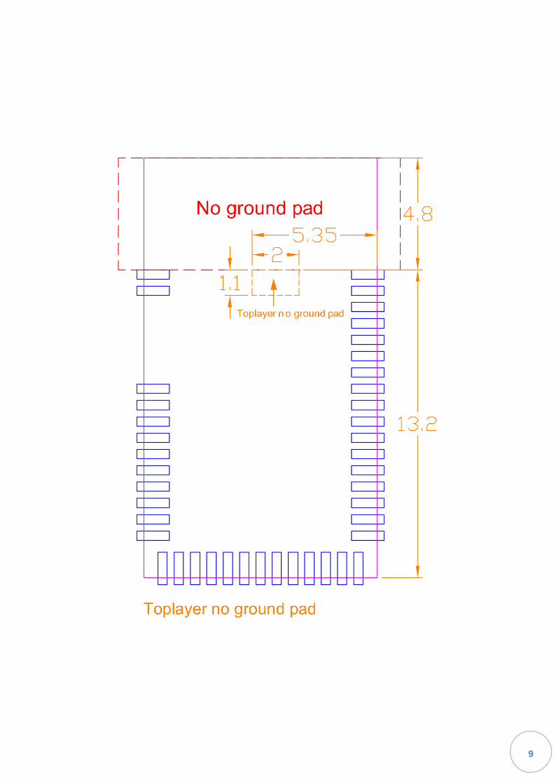
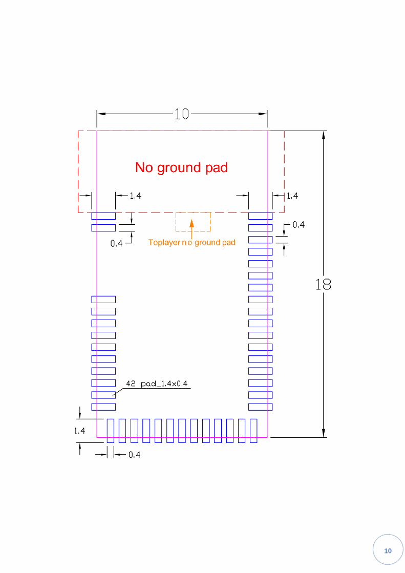
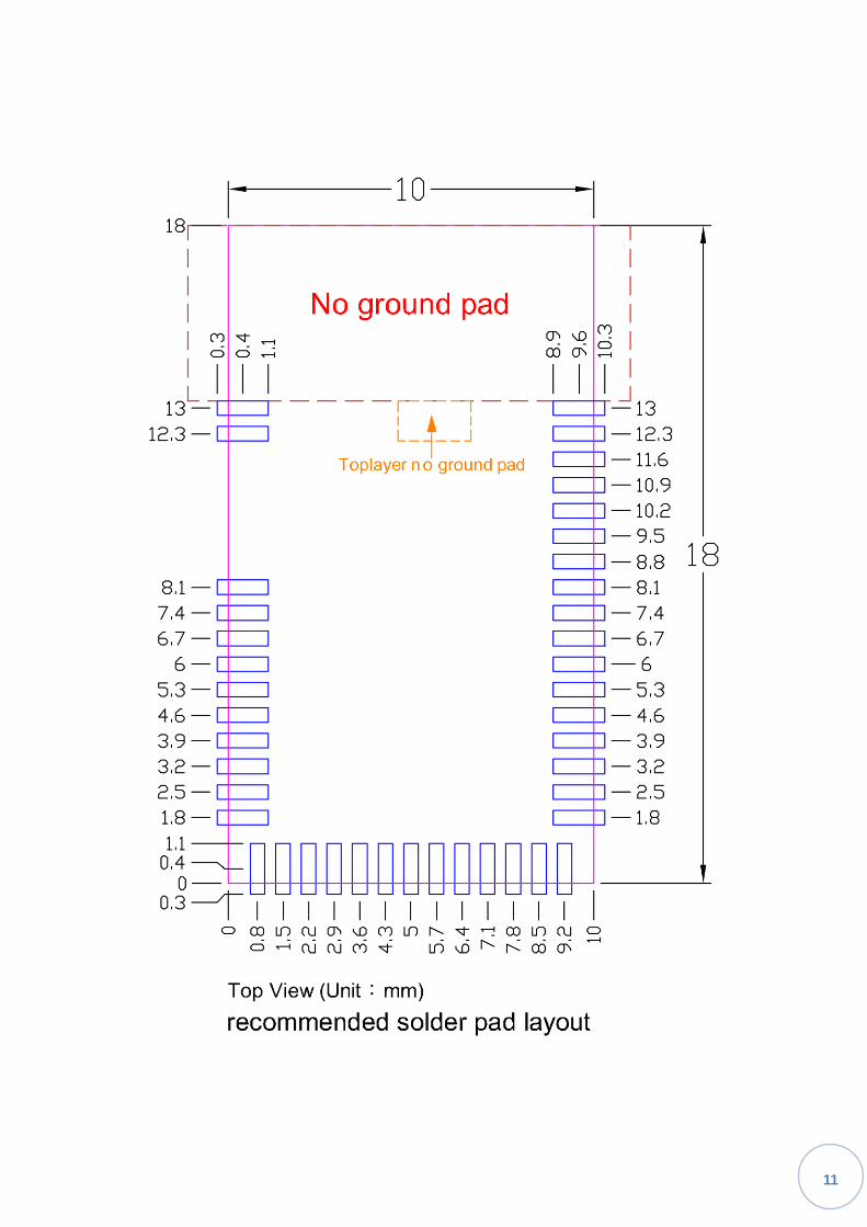
2.2. Recommended Layout of Solder Pad
Graphs are all in Top View, Unit in mm.
9
10
11
12
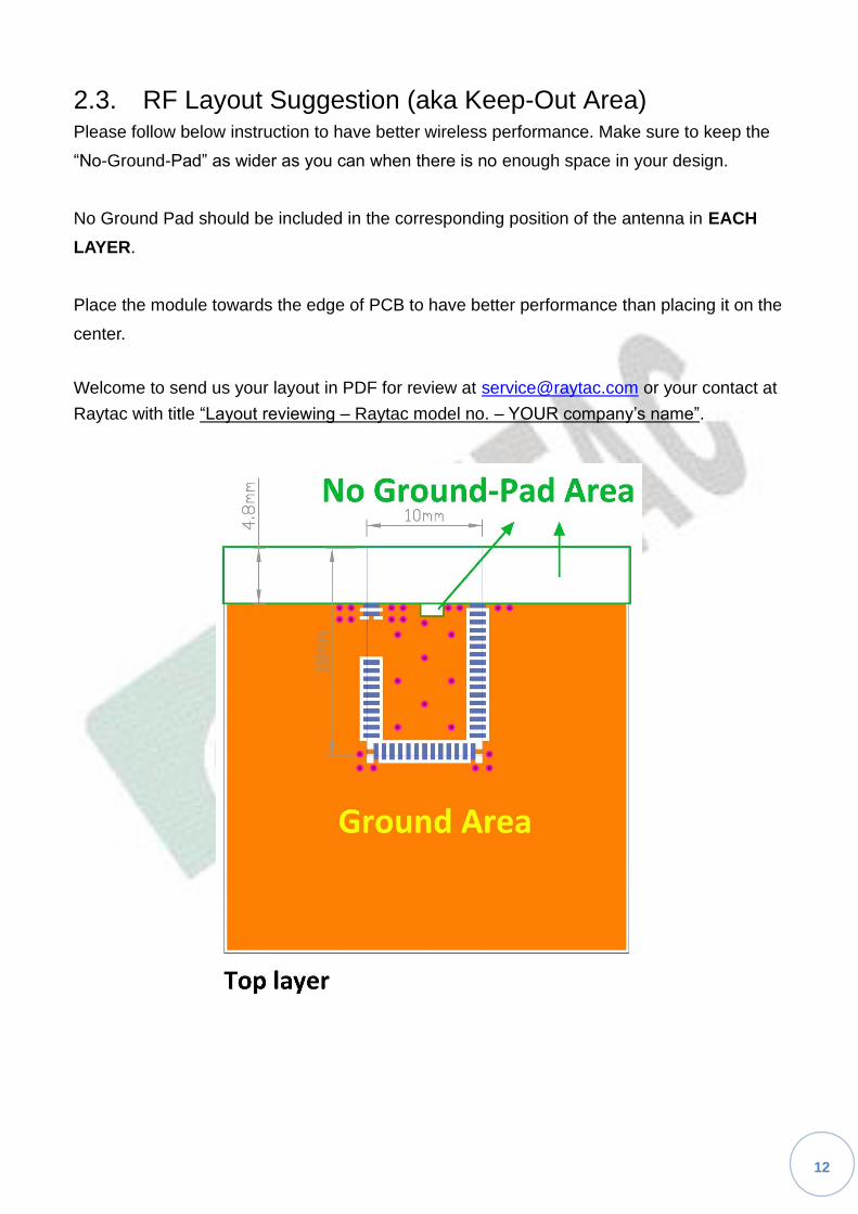
2.3. RF Layout Suggestion (aka Keep-Out Area)Please follow below instruction to have better wireless performance. Make sure to keep the
“No-Ground-Pad” as wider as you can when there is no enough space in your design.
No Ground Pad should be included in the corresponding position of the antenna in EACH
LAYER.
Place the module towards the edge of PCB to have better performance than placing it on the
center.
Welcome to send us your layout in PDF for review at [email protected] or your contact at
Raytac with title “Layout reviewing – Raytac model no. – YOUR company’s name”.

13
14
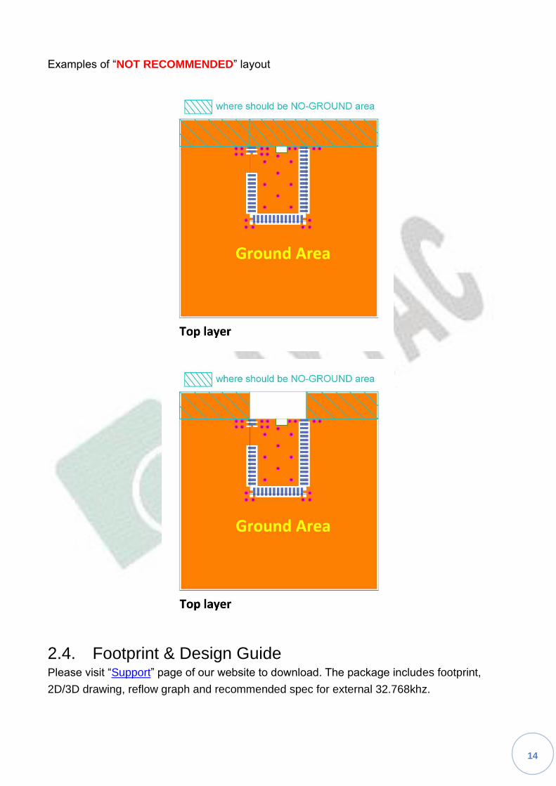
Examples of “NOT RECOMMENDED” layout
2.4. Footprint & Design GuidePlease visit “Support” page of our website to download. The package includes footprint,
2D/3D drawing, reflow graph and recommended spec for external 32.768khz.

15
2.5. Pin Assignment
Pin No. Name Pin function Description
(1)(2) GND Ground The pad must be connected to a solid ground plane
(3) AVDD Power Analog power supply
(4) P0.21 Digital I/O General-purpose digital I/O
(5) P0.22 Digital I/O General-purpose digital I/O
(6) P0.23 Digital I/O General-purpose digital I/O
(7) P0.24 Digital I/O General-purpose digital I/O
(8) P0.25 Digital I/O General-purpose digital I/O
(9)
P0.26 Digital I/O General-purpose digital I/O
AIN0 Analog input ADC input 0
XL2 Analog output Connector for 32.768KHz crystal
(10)
P0.27 Digital I/O General-purpose digital I/O
AIN1 Analog input ADC input 1
XL1 Analog input Connector for 32.768KHz crystal or external 32.768KHz
clock reference
(11) P0.28 Digital I/O General-purpose digital I/O
(12) P0.29 Digital I/O General-purpose digital I/O
(13) GND Ground The pad must be connected to a solid ground plane
(14) VDD Power Power supply
(15) DCC Power DC/DC output voltage to external LC filter
(16) P0.30 Digital I/O General-purpose digital I/O
(17) P0.00 Digital I/O General-purpose digital I/O
AREF0 Analog input ADC Reference voltage
(18) P0.01 Digital I/O General-purpose digital I/O
AIN2 Analog input ADC input 2
(19) P0.02 Digital I/O General-purpose digital I/O
AIN3 Analog input ADC input 3
(20) P0.03 Digital I/O General-purpose digital I/O
AIN4 Analog input ADC input 4

16
Pin No. Name Pin function Description
(21) P0.04 Digital I/O General-purpose digital I/O
AIN5 Analog input ADC input 5
(22) P0.05 Digital I/O General-purpose digital I/O
AIN6 Analog input ADC input 6
(23)
P0.06 Digital I/O General-purpose digital I/O
AIN7 Analog input ADC input 7
AREF1 Analog input ADC Reference voltage
(24) P0.07 Digital I/O General-purpose digital I/O
(25) GND Ground The pad must be connected to a solid ground plane
(26) P0.08 Digital I/O General-purpose digital I/O
(27) P0.09 Digital I/O General-purpose digital I/O
(28) P0.10 Digital I/O General-purpose digital I/O
(29) P0.11 Digital I/O General-purpose digital I/O
(30) P0.12 Digital I/O General-purpose digital I/O
(31) P0.13 Digital I/O General-purpose digital I/O
(32) P0.14 Digital I/O General-purpose digital I/O
(33) P0.15 Digital I/O General-purpose digital I/O
(34) P0.16 Digital I/O General-purpose digital I/O
(35) SWDIO/RESET Digital I/O System reset (active low). Also HW debug and flash
programming
(36) SWDCLK Digital input HW debug and flash programming.
(37) P0.17 Digital I/O General-purpose digital I/O
(38) P0.18 Digital I/O General-purpose digital I/O
(39) P0.19 Digital I/O General-purpose digital I/O
(40) P0.20 Digital I/O General-purpose digital I/O
(41) DEC2 Power Power supply decoupling. Low voltage mode VCC
(42) GND Ground The pad must be connected to a solid ground plane
1 Digital I/O pad with 5mA source/sink capability.

17
3. Main Chip Solution
RF IC Crystal Frequency
Nordic NRF51822 16MHZ
16MHz crystal is already inside the module.

18
4. Shipment Packaging Information
Marking Model
Red
MDBT40-256V3 MDBT40-P256V3
Yellow
MDBT40-256RV3 MDBT40-P256RV3
Modules produced in 2021 with date code 101 and later have marking with only one red
dot or one yellow dot.
- Unit Weight of Module:
MDBT40 Series: 0.88 g (±0.02 g) ; MDBT40-P Series: 0.78 g (±0.02 g)
- Packaging Type: Anti-static Tray or Tape & Reel.
19
4.1. Marking on Metal ShieldLabel context on metal shield is as below.
4.2. Packaging Info
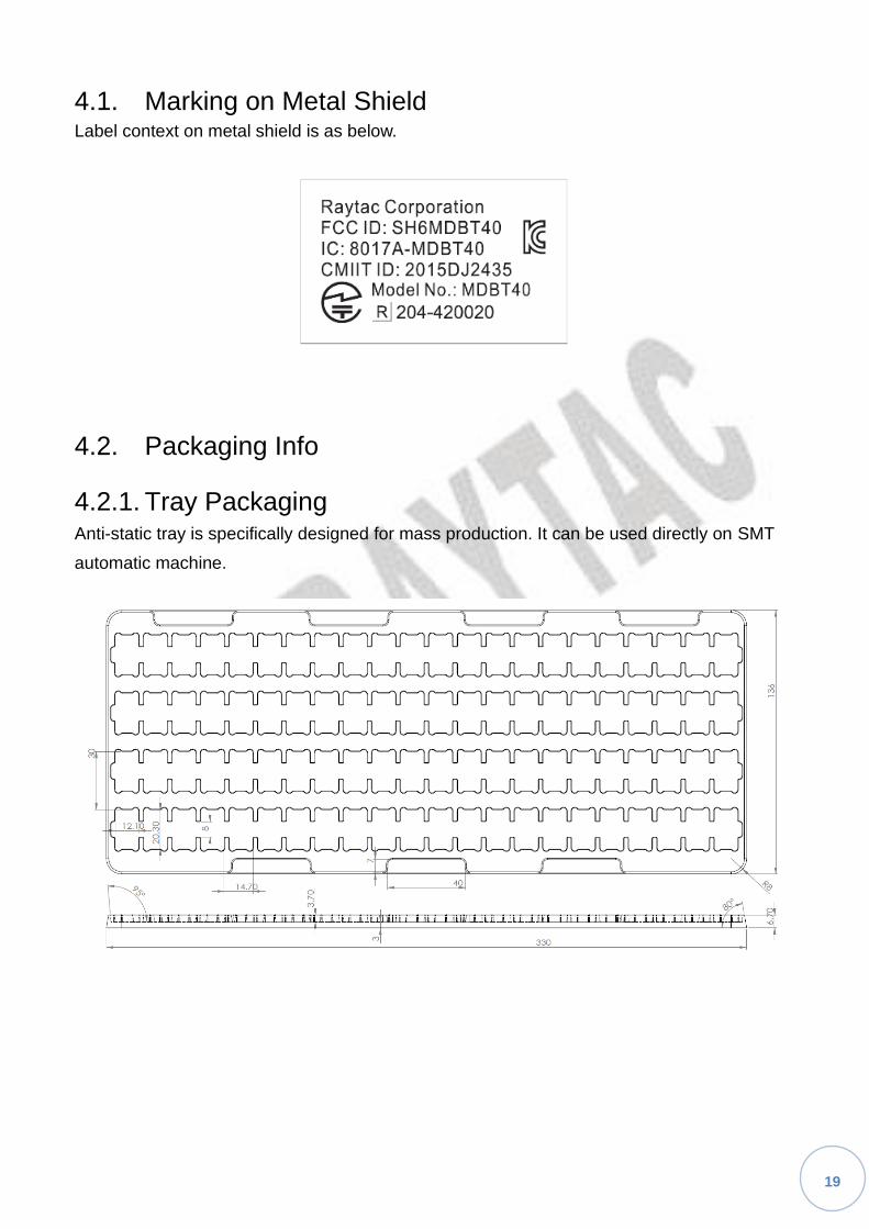
4.2.1. Tray PackagingAnti-static tray is specifically designed for mass production. It can be used directly on SMT
automatic machine.
20
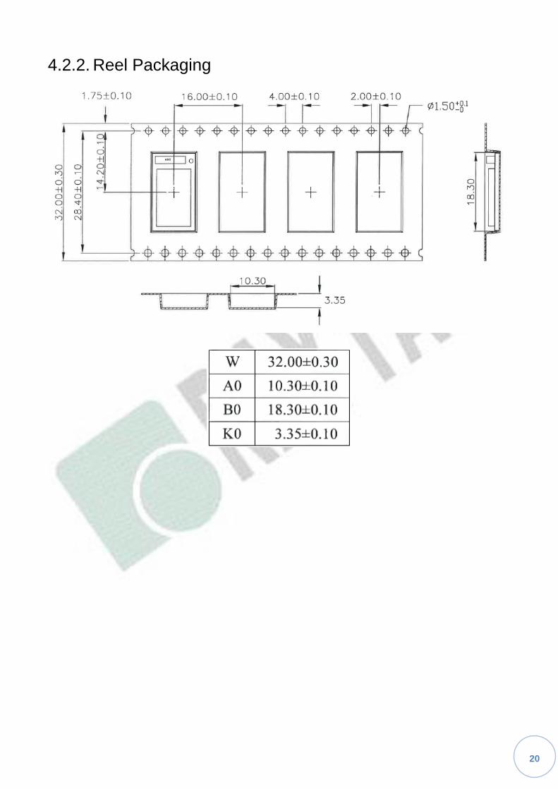
4.2.2. Reel Packaging

21
4.3. Order CodeEach model has two options of packaging. Please use following part no. when placing order
to us.
Model Tray Tape & Reel
MDBT40-256V3 MD-240A1-S32 MD-240A1-S32R
MDBT40-P256V3 MD-240A1-S33 MD-240A1-S33R
MDBT40-256RV3 MD-240A1-S26 MD-240A1-S26R
MDBT40-P256RV3 MD-240A1-S30 MD-240A1-S30R
MPQ of Reel packaging is 1,200 pcs and Tray packaging is 88 pcs.

22
5. Specification
Any technical spec shall refer to Nordic’s official documents as final reference. Contents
below are from “nRF51822 Specification for Extended Industrial Temperature Range” and
“nRF51822 Product Specification v3.3”, please click to download full spec.
5.1. Industrial Temperature RangeIndustrial temperature range is applied in below IC.
nRF51822 variant Build Code Raytac Model #
QFAA Hx0 MDBT40-256V3
MDBT40-P256V3
Operating conditions of supported industrial temperature:
Other changes are including:
(1) 2.4Ghz transceiver: not supported 1Mbps data rates
(2) Not support 1.8V low voltage mode.
When use above modules within -25℃ to 75℃, please see 5.3 Operation Conditions
and 5.4 Electrical Specifications to know its normal operating spec.

23
5.2. Absolute Maximum Ratings
5.3. Operation Conditions

24
5.4. Electrical Specifications
5.4.1. General Radio Characteristics
5.4.2. Radio Current Consumption
25
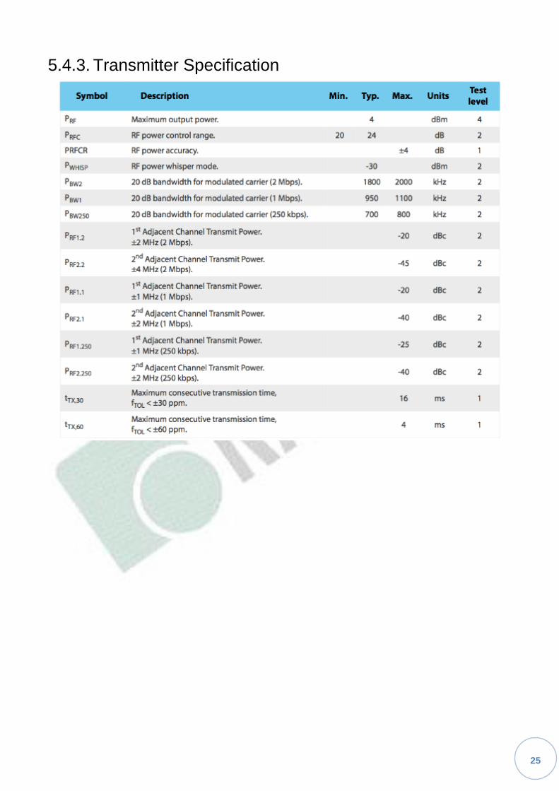
5.4.3. Transmitter Specification

26
5.4.4. Receiver Specifications

27

28
5.4.5. Radio Timing Parameters
5.4.6. RSSI Specifications
5.4.7. CPU

29
5.4.8. Power Management

30
6. Block Diagram

31
7. Antenna
7.1. MDBT40 Series

32
33
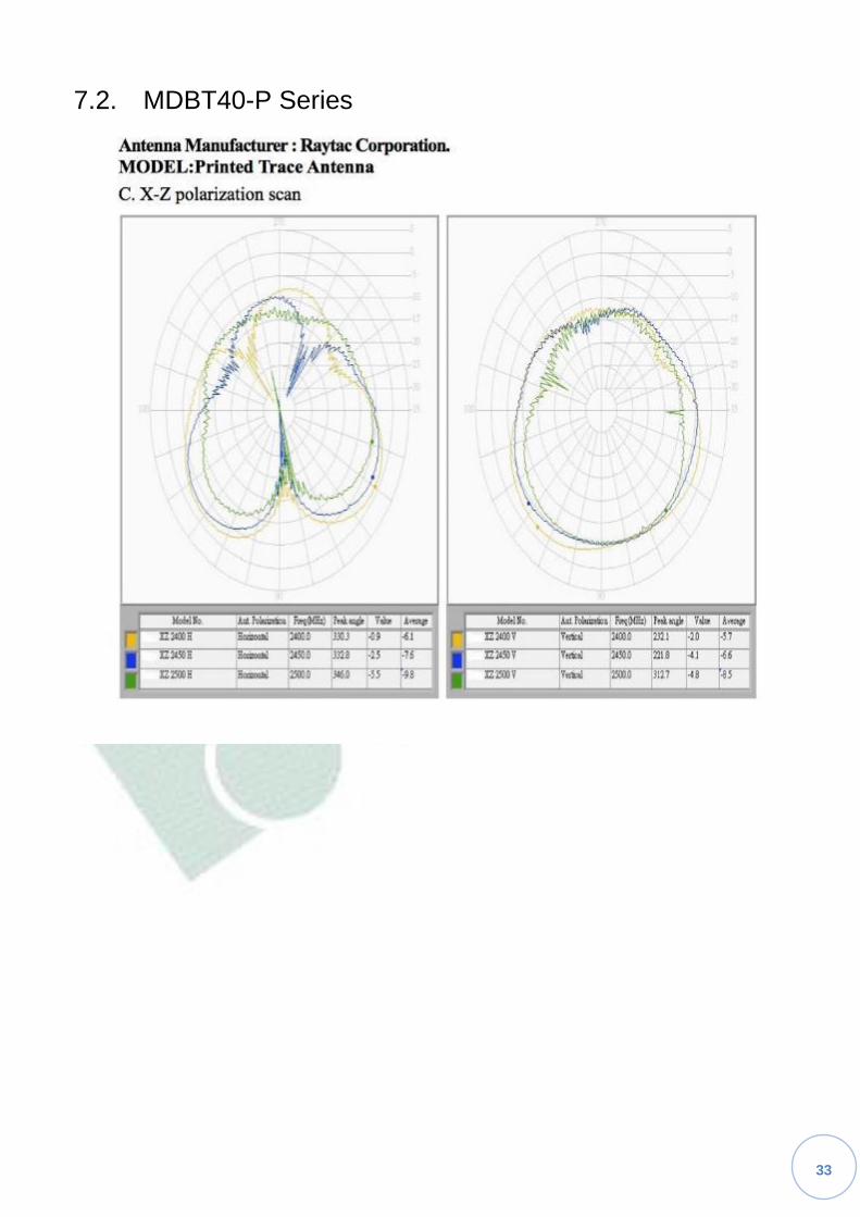
7.2. MDBT40-P Series
34
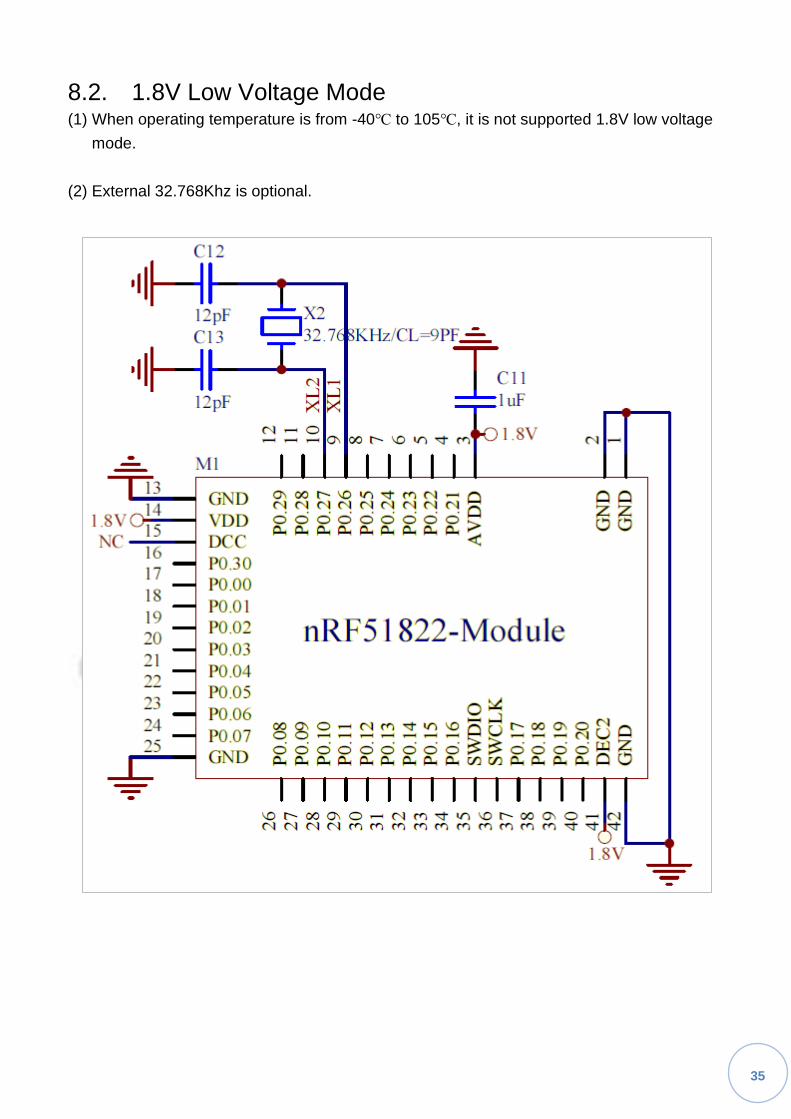
8. Reference Circuit
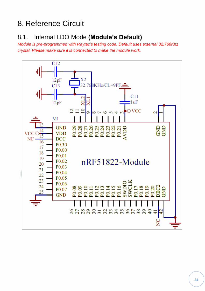
8.1. Internal LDO Mode (Module’s Default)Module is pre-programmed with Raytac’s testing code. Default uses external 32.768Khz
crystal. Please make sure it is connected to make the module work.
35
8.2. 1.8V Low Voltage Mode(1) When operating temperature is from -40℃ to 105℃, it is not supported 1.8V low voltage
mode.
(2) External 32.768Khz is optional.

36
8.3. Internal DC/DC Converter ModeExternal 32.768Khz is optional.
37
9. Certification
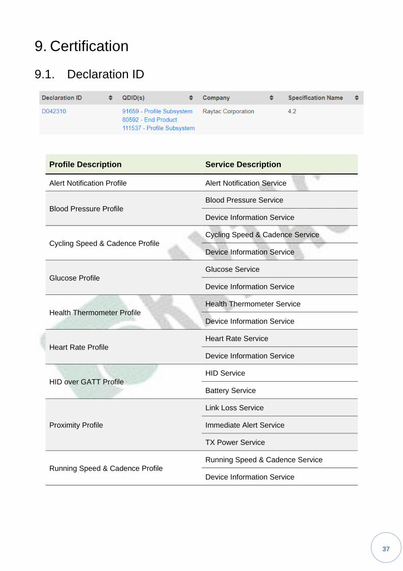
9.1. Declaration ID
Profile Description Service Description
Alert Notification Profile Alert Notification Service
Blood Pressure Profile Blood Pressure Service
Device Information Service
Cycling Speed & Cadence Profile Cycling Speed & Cadence Service
Device Information Service
Glucose Profile Glucose Service
Device Information Service
Health Thermometer Profile Health Thermometer Service
Device Information Service
Heart Rate Profile Heart Rate Service
Device Information Service
HID over GATT Profile HID Service
Battery Service
Proximity Profile
Link Loss Service
Immediate Alert Service
TX Power Service
Running Speed & Cadence Profile Running Speed & Cadence Service
Device Information Service

38
9.2. FCC Certificate (USA)

39
9.3. TELEC Certificate (Japan)

40
9.4. NCC Certificate (Taiwan)
MDBT40 Series

41
MDBT40-P Series
42
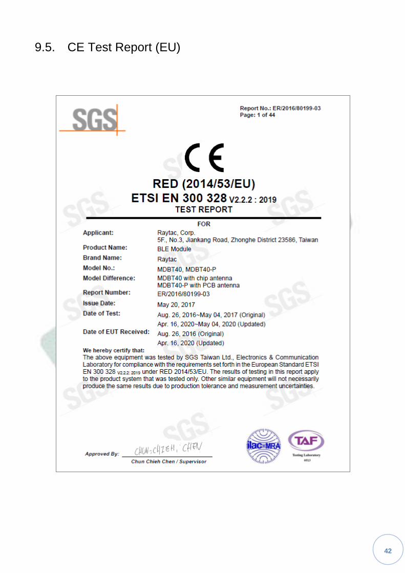
9.5. CE Test Report (EU)

43

44
9.6. IC Certificate (Canada)

45
9.7. SRRC Certificate (China)
46
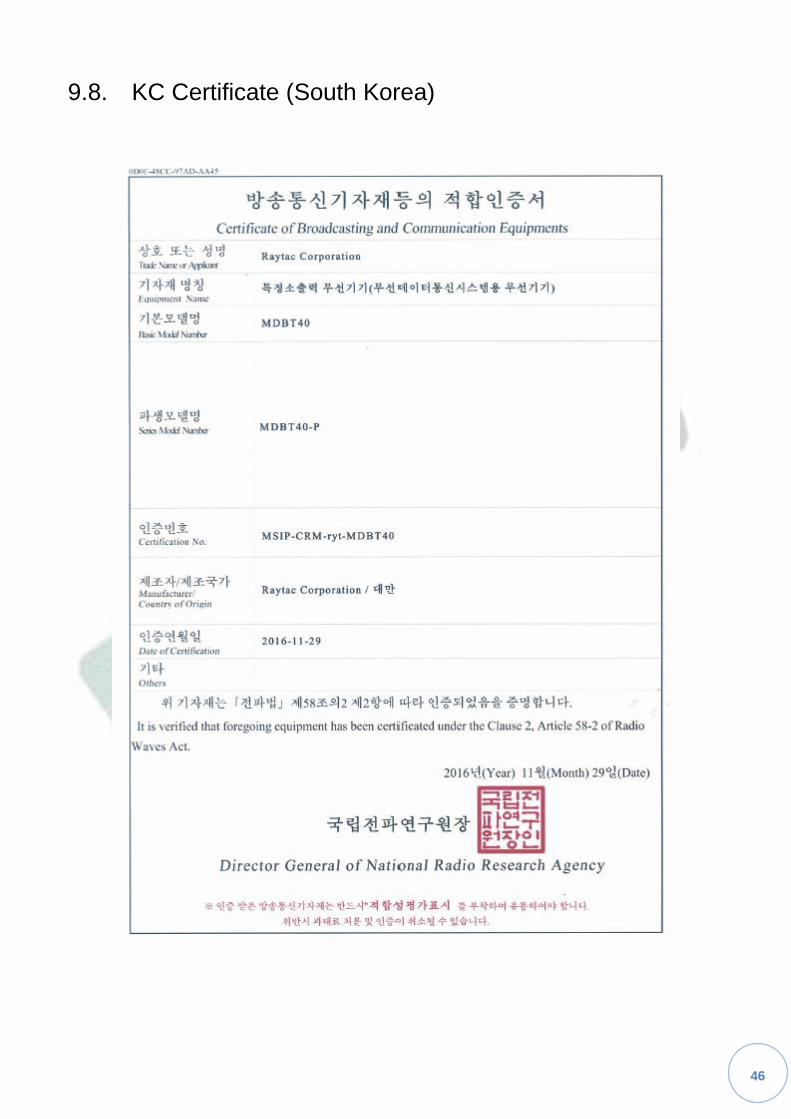
9.8. KC Certificate (South Korea)

47
9.9. RCM Test Report (Australia & New Zealand)
48
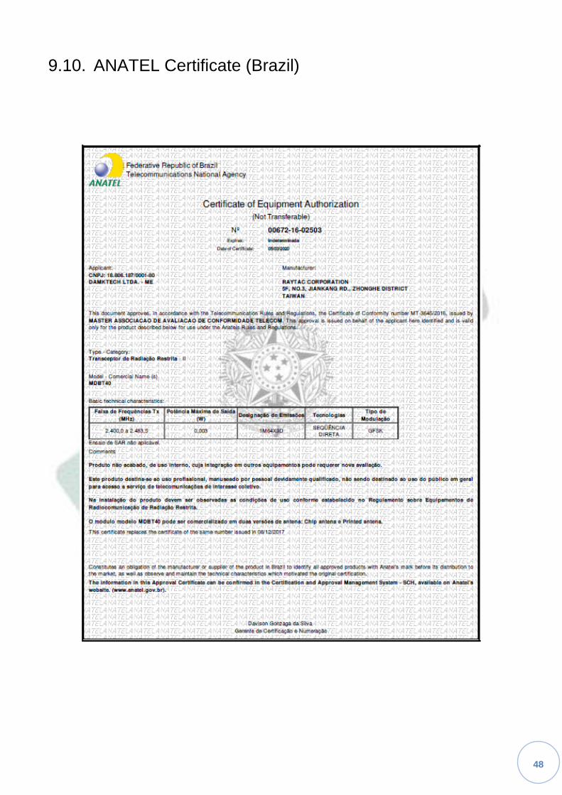
9.10. ANATEL Certificate (Brazil)
49
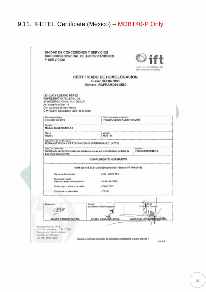
9.11. IFETEL Certificate (Mexico) – MDBT40-P Only

50

51
9.12. RoHS & REACH ReportPlease visit “Support” page of our website to download.
9.13. Reliability Test ReportPlease visit “Support” page of our website to download.
9.14. End-Product LabelIt is suggested using following content adding to package or user manual or label to obey the
regulation. Any rules of end-product label shall refer to each certification for final reference.
9.14.1. FCC (USA)The FCC statement should be included in the user manual when there is no enough space on
label. Otherwise, it should be included on the label.
“This device complies with part 15 of the FCC rules. Operation is subject to the following two
conditions. (1) This device may not cause harmful interference. (2) This device must accept
any interference received, including interference that may cause undesired operation.”
The final end product must be labeled in a visible area with the following: “Contain FCC ID:
SH6MDBT40”.
9.14.2. TELEC (Japan)When manufacturer is placing the product on the Japanese market, the product must be
affixed with the following Specified Radio Equipment marking:

52
9.14.3. NCC (Taiwan)請依下列標籤式樣自製標籤,標貼或印鑄於器材本體明顯處,始得販賣或公開陳列。
Series 標籤樣式
MDBT40 Series
MDBT40-P Series
以 MDBT40為例,平台廠商必須於平台上標示字樣「本產品內含射頻模組:ID編號
CCAF15LP0280T1」。
「平台」定義如下:若器材組裝本案模組,消費者仍能正常使用該器材主要功能,該器材得視
為平台。若器材不組裝本案模組,消費者不能正常使用該器材主要功能,該器材不能視為平台。
該類不同廠牌型號器材組裝本案審驗模組後,須分別申請型式認證。

53
9.14.4. IC (Canada)The IC statement should be included in the user manual when there is no enough space on
label. Otherwise, it should be included on the label.
“This device complies with Industry Canada license-exempt RSS Standard(s). Operation is
subject to the following two conditions. (1) This device may not cause harmful interference. (2)
This device must accept any interference received, including interference that may cause
undesired operation.
Le présent appareil est conforme aux CNR d'Industrie Canada applicables aux appareils
radio exempts de licence.L'exploitation est autorisée aux deux conditions suivantes: (1)
l'appareil ne doit pas produire de brouillage, et (2) l'utilisateur de l'appareil doit accepter tout
brouillage radioélectrique subi, même si le brouillage est susceptible d'en compromettre le
fonctionnement.”
The final end product must be labeled in a visible area with the following: “Contain IC ID:
8017A-MDBT40”.

54
10. Notes and CautionsModule is not designed to last for a lifetime. Like general products, it is expected to be worn
out after continuous usage through the years. To assure that product will perform better and
last longer, please make sure you:
⚫ Follow the guidelines of this document while designing circuit/end-product. Any
discrepancy of core Bluetooth technology and technical specification of IC should refer to
definition of Bluetooth Organization and Nordic Semiconductor as final reference.
⚫ Do not supply voltage that is not within range of specification.
⚫ Eliminate static electricity at any cost when working with the module as it may cause
damage. It is highly recommended adding anti-ESD components to circuit design to
prevent damage from real-life ESD events. Anti-ESD methods can be also applied in
mechanical design.
⚫ Do not expose modules under direct sunlight for long duration. Modules should be kept
away from humid and salty air conditions, and any corrosive gasses or substances. Store
it within -40℃ to +125℃ before and after installation.
⚫ Avoid any physical shock, intense stress to the module or its surface.
⚫ Do not wash the module. No-Clean Paste is used in production. Washing it will oxidize
the metal shield and have chemistry reaction with No-Clean Paste. Functions of the
module are not guaranteed if it has been washed.
The module is not suitable for life support device or system and not allowed to be used in
destructive device or systems in any direct or indirect ways. The customer agrees to
indemnify Raytac for any losses when applying modules in applications such as the ones
described above.
55
11. Useful Links
⚫ Nordic Infocenter: https://infocenter.nordicsemi.com/index.jsp
All the necessary technical files and software development kits of Nordic’s chip are on
this website.
⚫ Nordic DevZone: https://devzone.nordicsemi.com/questions/
A highly recommended website for firmware developer. Interact with other developers
and Nordic’s employees will help with your questions. The site also includes tutorials in
detail to help you get started.
⚫ Official Page of nRF51822:
https://www.nordicsemi.com/eng/Products/Bluetooth-low-energy/nRF51822
A brief introduction to nRF51822 and download links for Nordic’s developing software
and SoftDevices.
56
Full List of Raytac’s BLE Modules
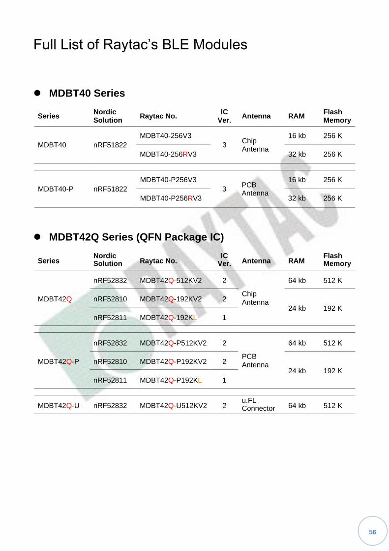
⚫ MDBT40 Series
Series Nordic Solution
Raytac No. IC
Ver. Antenna RAM
Flash Memory
MDBT40 nRF51822
MDBT40-256V3
3 Chip Antenna
16 kb 256 K
MDBT40-256RV3 32 kb 256 K
MDBT40-P nRF51822
MDBT40-P256V3
3 PCB Antenna
16 kb 256 K
MDBT40-P256RV3 32 kb 256 K
⚫ MDBT42Q Series (QFN Package IC)
Series Nordic Solution Raytac No.
IC Ver. Antenna RAM
Flash Memory
MDBT42Q
nRF52832 MDBT42Q-512KV2 2
Chip
Antenna
64 kb 512 K
nRF52810 MDBT42Q-192KV2 2
24 kb 192 K
nRF52811 MDBT42Q-192KL 1
MDBT42Q-P
nRF52832 MDBT42Q-P512KV2 2
PCB
Antenna
64 kb 512 K
nRF52810 MDBT42Q-P192KV2 2
24 kb 192 K
nRF52811 MDBT42Q-P192KL 1
MDBT42Q-U nRF52832 MDBT42Q-U512KV2 2 u.FL Connector 64 kb 512 K

57
⚫ MDBT42 Series (WLCSP Package IC)
Series Nordic Solution
Raytac No. IC
Ver. Antenna RAM
Flash Memory
MDBT42
nRF52832
MDBT42-512KV2
2
Chip Antenna
64 kb 512 K
MDBT42-P MDBT42-P512KV2 PCB Antenna
⚫ MDBT42V Series (WLCSP Package IC)
Series Nordic
Solution Raytac No. IC
Ver. Antenna RAM Flash
Memory
MDBT42V
nRF52832
MDBT42V-512KV2
2
Chip
Antenna 64 kb 512 K
MDBT42V-P MDBT42V-P512KV2 PCB
Antenna
⚫ MDBT42T Series (WLCSP Package IC)
Series Nordic
Solution Raytac No. IC
Ver. Antenna RAM Flash
Memory
MDBT42T
nRF52805
MDBT42T-192K
1
Chip
Antenna 24 kb 192 K
MDBT42T-P MDBT42T-P192K PCB
Antenna
⚫ MDBT42TV Series (WLCSP Package IC)
Series Nordic
Solution Raytac No. IC
Ver. Antenna RAM Flash
Memory
MDBT42TV
nRF52805
MDBT42TV-192K
1
Chip
Antenna 24 kb 192 K
MDBT42TV-P MDBT42TV-P192K PCB
Antenna

58
⚫ MDBT50Q Series (aQFN Package IC)
Series Nordic
Solution Raytac No. IC
Ver. Antenna RAM Flash
Memory
MDBT50Q
nRF52840 MDBT50Q-1MV2 2 Chip
Antenna
256 kb 1 MB
nRF52833 MDBT50Q-512K 1 128 kb 512 kb
MDBT50Q-P
nRF52840 MDBT50Q-P1MV2 2 PCB
Antenna
256 kb 1 MB
nRF52833 MDBT50Q-P512K 1 128 kb 512 kb
MDBT50Q-U
nRF52840 MDBT50Q-U1MV2 2 u.FL
Connector
256 kb 1 MB
nRF52833 MDBT50Q-U512K 1 128 kb 512 kb
Dongle nRF52840 MDBT50Q-RX 1, 2 PCB
Antenna 256 kb 1 MB
⚫ MDBT50 Series (QFN Package IC)
Series Nordic
Solution Raytac No. IC
Ver. Antenna RAM Flash
Memory
MDBT50 nRF52820 MDBT50-256R 1 Chip
Antenna 256 kb 32 K
MDBT50-P nRF52820 MDBT50-P256R 1 PCB
Antenna 256 kb 32 K
59
Release Note⚫ 2015/02/13 Version A1
(1) Added NCC certificate in Chapter 10: Certification.
⚫ 2015/04/29 Version A2
(1) Added MDBT40-P Spec, RoHS Report and List of Raytac’s Model no.
(2) Updated Chapter 8: Reference Circuit
(3) Updated Chapter 9: Carrier Keep-Out Area
(4) Updated Chapter 12: BT 4.0 Product Certification Cost Comparison Chart
(5) Updated Chapter 13: nRF51 IC Compatibility with SDK & Softdevice.
⚫ 2015/07/01 Version A3
(1) Added IC (Canada) & SRRC (China) certificates in Chapter 10: Certification.
⚫ 2015/11/03 Version A4
(1) Revised layout guide for MDBT40 series in Chapter 2: Product Dimension.
(2) Updated Chapter 5: Specification.
(3) Updated List of Raytac’s Model no.
(4) Removed info of V2 module from Chapter 4: Shipment Packaging Information.
(5) Added reliability test in Chapter 10: Certification.
⚫ 2017/01/16 Version A5
(1) Updated List of Raytac model no.
(2) Removed Chapter 9: Carrier Keep-Out Area and combined it with Chapter 2: Product
Dimension.
(3) Updated Chapter 4: Shipment Packaging Information.
(4) Updated Chapter 12: nRF51 IC Compatibility with SDK & Softdevice.
(5) Added KC (South Korea) Certificate, RoHS & REACH reports in Chapter 9:
Certification.
⚫ 2017/05/19 Version A6
(1) Updated List of Raytac’s Model no.

60
(2) Added link for footprint & design guide in Chapter 2: Production Dimension.
(3) Updated CE reports to new RED directives in Chapter 9: Certification.
⚫ 2017/07/19 Version A7
(1) Updated section 3 and section 4 of Chapter 2: Product Dimension.
(2) Updated List of Raytac’s Model no.
⚫ 2018/06/14 Version A8
(1) Updated spec in section 2 of Chapter 1: Introduction and Chapter 5: Specification
(2) Updated links for 2018 RoHS & REACH reports.
(3) Replaced Chapter 10: Current Consumption Reference Data with Notes and
Cautions
(4) Replaced Chapter 11: BT 4.1 Product Certification Cost Comparison Chart with
Useful Links.
(5) Removed Chapter 12: nRF51 IC Compatibility with SDK & Softdevice.
⚫ 2018/11/15 Version A9
(1) Added Mesh Profile in section 3 of Chapter 1: Product Information.
(2) Updated drawing & link of footprint & design guide in Chapter 2.
(3) Removed info of MDBT40-128V3 /P128V3 and added tray info in Chapter 4:
Shipment Packaging Information.
(4) Added source of reference and updated Chapter 5: Specification.
(5) Added new SIG BT 4.2 certification info, RCM report, ANATEL (Brazil) certificate,
CNC (Argentina), IFETEL (Mexico) certificate and updated link of RoHS & REACH
reports in Chapter 9: Certification.
(6) Added “no-washing” warning in Chapter 10: Notes and Cautions.
⚫ 2019/10/03 Version A10
(1) Added tolerance information of PCB size in Chapter 2: Product Dimension.
(2) Updated withdrawn information of SIG and removed Argentina certificate in Chapter 9:
Certification.

61
⚫ 2019/11/28 Version A11
(1) Corrected information of size of PCB and tolerance in Chapter 2: Product Dimension.
(2) Added nRF52833 module in Full List of Raytac’s BLE Modules.
⚫ 2020/06/10 Version A12
(1) Moved section 3 in Chapter 1: Introduction to section 1 of Chapter 9: Certification.
(2) Updated ANATEL certificate and CE reports EN300.328 V2.2.2 & EN62368-1 in
Chapter 9: Certification.
(3) Updated the Full List of Raytac’s BLE module.
⚫ 2020/12/14 Version A13
(1) Added description about new marking of the module in Chapter 4: Shipment
Packaging Information.
(2) Updated SRRC certificate in Chapter 9: Certification.
(3) Updated the Full List of Raytac BLE Modules.
⚫ 2021/01/05 Version A14
(1) Added information of T&R in Chapter 4: Shipment Packaging Information.
⚫ 2021/07/23 Version A15
(1) Updated graphs in section 2 of Chapter 2: Product Dimension.
(2) Updated information of T&R in Chapter 4: Shipment Packaging Information.
(3) Removed info MDBT40-n256V3 in Chapter 5: Specification
(4) Added the download link for reliability test in section 13 of Chapter 9: Certification