measured characteristics of selected s-band … research laboratory adelphi, md 20783-1197...
TRANSCRIPT

Measured Characteristics of Selected S-Band Coaxial-to-
Waveguide Adaptors
by William O. Coburn
ARL-TN-220 July 2004 Approved for public release; distribution unlimited.

NOTICES
Disclaimers The findings in this report are not to be construed as an official Department of the Army position unless so designated by other authorized documents. Citation of manufacturer’s or trade names does not constitute an official endorsement or approval of the use thereof. Destroy this report when it is no longer needed. Do not return it to the originator.

Army Research Laboratory Adelphi, MD 20783-1197
ARL-TN-220 July 2004
Measured Characteristics of Selected S-Band Coaxial-to-Waveguide Adaptors
William O. Coburn
Sensors and Electron Devices Directorate, ARL Approved for public release; distribution unlimited.
ii
REPORT DOCUMENTATION PAGE Form Approved OMB No. 0704-0188
Public reporting burden for this collection of information is estimated to average 1 hour per response, including the time for reviewing instructions, searching existing data sources, gathering and maintaining the data needed, and completing and reviewing the collection information. Send comments regarding this burden estimate or any other aspect of this collection of information, including suggestions for reducing the burden, to Department of Defense, Washington Headquarters Services, Directorate for Information Operations and Reports (0704-0188), 1215 Jefferson Davis Highway, Suite 1204, Arlington, VA 22202-4302. Respondents should be aware that notwithstanding any other provision of law, no person shall be subject to any penalty for failing to comply with a collection of information if it does not display a currently valid OMB control number. PLEASE DO NOT RETURN YOUR FORM TO THE ABOVE ADDRESS.
1. REPORT DATE (DD-MM-YYYY)
July 2004 2. REPORT TYPE
Final 3. DATES COVERED (From - To)
11/2003 to 2/2004 5a. CONTRACT NUMBER
5b. GRANT NUMBER
4. TITLE AND SUBTITLE
Measured Characteristics of Selected S-Band Coaxial-to-Waveguide Adaptors
5c. PROGRAM ELEMENT NUMBER
5d. PROJECT NUMBER
5e. TASK NUMBER
6. AUTHOR(S)
William O. Coburn
5f. WORK UNIT NUMBER
7. PERFORMING ORGANIZATION NAME(S) AND ADDRESS(ES)
U.S. Army Research Laboratory ATTN: AMSRD-ARL-SE-RU 2800 Powder Mill Road Adelphi, MD 20783-1197
8. PERFORMING ORGANIZATION REPORT NUMBER
ARL-TN-220
10. SPONSOR/MONITOR'S ACRONYM(S)
9. SPONSORING/MONITORING AGENCY NAME(S) AND ADDRESS(ES)
U.S. Army Research Laboratory 2800 Powder Mill Road Adelphi, MD 20783-1197
11. SPONSOR/MONITOR'S REPORT NUMBER(S)
12. DISTRIBUTION/AVAILABILITY STATEMENT
Approved for public release; distribution unlimited.
13. SUPPLEMENTARY NOTES 14. ABSTRACT
A design procedure for a leaky wave antenna fabricated in slitted waveguide was developed based on the analysis of Goldstone and Oliner (1). The use of dielectric loading in slitted rectangular or dual-ridged waveguide is one way to influence the antenna performance. An experimental fixture to evaluate the transmission line characteristics of miniaturized dual-ridged waveguide was fabricated to allow for dielectric loading in the ridge section. The goal is to obtain experimental validation of the theory as applied to a specific leaky dual-ridged waveguide loaded with conventional engineering plastics. As a first step the effect of the coaxial-to-waveguide adaptors needed to feed and terminate the experimental fixture must be determined. The offset short method is used to characterize commercial microwave adaptors requiring at least three different waveguide lengths. Five different lengths of S-Band waveguide sections were available although some choices are more appropriate than others depending on the frequency range of interest. The experimental results are used to calculate the scattering parameters for five different microwave adaptors over the frequency range 2.8 to 3.2 GHz. The method and the limitations imposed by not being able to use optimized waveguide lengths are described. A summary of the adaptor characteristics is provided for the reference of other researchers so that the most appropriate part can be chosen for a given application. 15. SUBJECT TERMS
S-Band, WR-284, microwave adaptors, coaxial-to-waveguide adaptors
16. SECURITY CLASSIFICATION OF: 19a. NAME OF RESPONSIBLE PERSON William O. Coburn
a. REPORT
UNCLASSIFIED b. ABSTRACT
UNCLASSIFIED c. THIS PAGE
UNCLASSIFIED
17. LIMITATIONOF ABSTRACT
UL
18. NUMBER OF PAGES
22 19b. TELEPHONE NUMBER (Include area code) 301-394-2705
Standard Form 298 (Rev. 8/98) Prescribed by ANSI Std. Z39.18

iii
Contents
List of Figures iiv
List of Tables iiv
Acknowledgement v
1. Purpose 1
2. Background 1
3. Experimental Method 5
4. Results 7 4.1 FXR Model S601A..........................................................................................................8
4.2 FXR Model S601B..........................................................................................................9
4.3 Narda Model 614A and HP Model S281A ...................................................................10
5. Summary 11
6. References 13
Distribution List 14

iv
List of Figures
Figure 1. (a) The cross section of an air-filled, symmetric, dual-ridged waveguide. (b) An approximate equivalent circuit for an air-filled, symmetric, dual-ridged waveguide................2
Figure 2. A scale drawing of the dual-ridged waveguide cross-section with removable dielectric filled center section and bolted axial flange..............................................................3
Figure 3. Photograph of WR-284 microwave adaptors. (a) View of coaxial probe. (b) View of coaxial input. ........................................................................................................................4
Figure 4. Block diagram of the WR-284 microwave adaptor experimental arrangement.............4 Figure 5. Electrical length of WR-284 waveguide sections. ..........................................................7 Figure 6. (a) Return and insertion loss obtained for the FXR601A adaptor when using L0 as
the reference length. (b) Standing Wave Ratio obtained for the FXR601A adaptor when using L0 as the reference length. ................................................................................................8
Figure 7. (a) Return and insertion loss obtained for the FXR601A adaptor when using L1 as the reference length. (b) Standing Wave Radio obtained for the FXR601A adaptor when using L1 as the reference length. ................................................................................................9
Figure 8. Standing Wave Ratio obtained for the FXR601A adaptor when using both L2 and L3................................................................................................................................................9
Figure 9. (a) Return and insertion loss obtained for the FXR601B adaptors using waveguide lengths L1, L3, and L4. (b) Standing Wave Ratio obtained for the FXR601B adaptors using waveguide lengths L1, L3, and L4. ..................................................................................10
Figure 10. (a) Return and insertion loss obtained for the Narda and HP adaptors using waveguide lengths L1, L3, and L4. (b) Standing Wave Ratio obtained for the Narda and HP adaptors using waveguide lengths L1, L3, and L4. .............................................................11
Figure 11. Standing Wave Ratio obtained for microwave adaptors using waveguide lengths L1, L3, and L4. ..........................................................................................................................12
List of Tables
Table 1. WR-284 Waveguide lengths used in the offset short method. .........................................6

v
Acknowledgement
The author acknowledges the assistance of Tim White in the accurate measurement of the waveguide lengths. His expertise in this measurement was critical to successfully implementing the experimental method.

vi
INTENTIONALLY LEFT BLANK.

1
1. Purpose
The physical structure of interest is a leaky waveguide, excited by a transverse electric (TE)10-mode (or H10-mode), with a long slit in the waveguide narrow-wall radiating into a half-space (i.e., an infinite flange approximation). The leaky wave antenna design procedure of Oliner (1) can be extended through an iterative procedure (2) and applied to the case of an asymmetric dual-ridged waveguide with variable width slit and dielectric filled ridge section (3). Based on this design procedure, an asymmetric dual-ridged waveguide was fabricated that allows for removable dielectric inserts in the ridge section. This dielectric-loaded dual-ridged waveguide is connected to S-Band (WR-284) coaxial-to-waveguide adaptors for measurement purposes. An impedance matching transition to rectangular waveguide was not attempted because the leaky waveguide would be fed as part of an element in an antenna array. In order to evaluate the closed waveguide the WR-284 microwave, adaptors must be characterized over the frequency range of interest, 2.8 to 3.2 GHz. The offset short experimental method is used with different lengths of bolted waveguide sections between the adaptor and shorting plate (4). The next step is to use the known adaptors to measure the transmission line characteristics and the antenna pattern obtained for the leaky dual-ridged waveguide experimental fixture.
2. Background
A dual-ridged waveguide is a rectangular waveguide with a centered rectangular ridge on both of its wide sides as shown in figure 1 (a) for the symmetric case. The structure requires determination of the guide wavelength
( )21c
g
λλ
λλ−
= (1)
since for the ridged waveguide the cutoff wavelength, λc is not simply related to the guide width, a. The transverse (to y) wavenumber is kz = 2π/λc, for the cutoff wavelength of each mode. The transverse resonance method provides the correct λc for each mode to satisfy the boundary conditions throughout the waveguide. Following Marcuvitz, the dominant mode propagation in an equivalent transverse network can be extended to the case of uniform dielectric loading in the ridged section (5). A solution for the propagation constant of leaky, dielectric-loaded, dual-ridged waveguide using the perturbation technique can be used to calculate the radiation pattern for different slit width profiles. But this analysis does not include the effect of microwave adaptors to feed and/or terminate the leaky waveguide.

2
x
z
x = b
0
Perfect conductor
z = a/2
y
z = aT
ε0, µ0 ε0, µ0
b0
a0
E
ε0, µ0 ε0, µ0
jB
T
Y0
a0/2
λcλc
Y0′
(a - a0)/2
(a) (b)
Figure 1. (a) The cross section of an air-filled, symmetric, dual-ridged waveguide. (b) An approximate equivalent circuit for an air-filled, symmetric, dual-ridged waveguide.
The dual-ridged leaky waveguide with uniform dielectric loading in the ridge section has some advantages for use in antenna arrays where feed systems can be carefully designed for optimum performance. At this stage, experimental data on a single leaky waveguide is required but limited by available microwave components and test equipment. A center operating frequency of f0 = 3 GHz is chosen so that the experimental fixture would have physical dimensions that could be accurately fabricated. The fixture is designed to allow different dielectric loading and uses WR-284 rectangular flanges to allow connection to standard S-Band waveguide components. The parameters of the experimental fixture are the waveguide width, a, height, b and the ridge width, a0 and height b0. The waveguide height is symmetric but the width has asymmetry w' = A2/A1 = 1.2, as shown in figure 2. A normalized ridge width, r = a0/a = 0.05, and normalized ridge height, r' = b0/b = 0.5, were chosen in the design procedure. The parameter b1/A1 = 0.5 so that b/a = 0.216 corresponds to roughly quarter-height waveguide (see figure 2). Fabrication is accomplished using soldered brass sheet stock (80-mils thick) with an axial flange holding the ridge sections having 1.5-in bolt spacing to allow disassembly. The normalized length is designed to be k0L = 20π for free space wavenumber k0, corresponding to ten wavelengths at the center frequency. The ridge section can be filled with different plastic inserts which have a machined groove to mate with the ridge section of the experimental fixture as shown in figure 2.

3
Figure 2. A scale drawing of the dual-ridged waveguide cross-section with removable dielectric filled center section and bolted axial flange.
The dielectric and conductor losses are calculated as independent loss mechanisms but for typical materials these losses are negligible. The S-Band adaptors are characterized by their scattering (S-) parameters which relate the two incident, [u], and reflected, [v], voltage waves at reference planes 1 and 2 by the scattering matrix [v] = [S] [u]. The leaky waveguide continuously loses energy along its length due to radiation so that a matched termination is not critical for performance. The impedance mismatch to the feed waveguide would then determine the input reflection coefficient, Γ, and transmission coefficient, T, where in terms of the S-parameters, Γ = S11 and T = S21 for matched termination. Performance is often characterized by the return loss (RL) and insertion loss (IL), or alternatively by the input standing wave ratio (SWR). These parameters are related by
120log , 20 log ,
1RL IL T SWR
+ Γ= Γ = =
− Γ (2)
This fixture includes WR-284 rectangular cover flanges for bolted connection to the input (feed) and output (termination) waveguide. Several coaxial-to-waveguide adaptors are available from Narda1 (Model 614A), Hewlett-Packard2 (Model S281A) and MicroLab/FXR3 (Models S601A, S601B and S601C). Many of these parts are no longer in production and the specifications are not readily available. Also, some damage was observed on all these parts so the actual performance may not meet the original specifications and must be measured. Typical specifications are SWR < 1.4 over the range 2.6 to 3.95 GHz corresponding to RL < –15 dB. These adaptors have Type-N Female coaxial inputs and WR-284 circular cover flanges as shown in figure 3. Short WR-284 waveguide extensions are used as needed to convert circular flanges to standard rectangular cover flanges as indicated in the block diagram shown in figure 4.
1 Narda Microwave Group, L3 Communications, New York, NY. 2 Hewlett-Packard USA, Palo Alto, CA. 3 F-R Machine Works, Inc., Electronics and X-Ray Division, Queens, NY.

4
Figure 3. Photograph of WR-284 microwave adaptors. (a) View of coaxial probe. (b) View of coaxial input.
Figure 4. Block diagram of the WR-284 microwave adaptor experimental arrangement.
Waveguide sections with circular flanges were primarily used with a circular to rectangular flange extension for connection to the rectangular shorting plate. One section of WR-284 with rectangular flanges was also used, where an extension is inserted between the circular flanged adaptor and the rectangular flanged waveguide. The Type-N coaxial input was adapted to an SMA connector using the same part for all the adaptors (shown mounted to the HP adaptor in figure 3). The measured data was obtained with a Wiltron4 37269A vector network analyzer (VNA), calibrated for input reflection measurements using the Wiltron K-Cal Kit Model 3652. These S-Band microwave adaptors all have dielectric sheathed coaxial probe designs except the FXR Model S601A (S/N 154) which does not use a dielectric coating (see figure 3).
4 Wiltron Company, Morgan Hill, CA.

5
3. Experimental Method
The offset short method with different lengths of WR-284 waveguide is used to calculate the S-parameters of the adaptor from the measured input reflection coefficients. A sliding short in WR-284 would be preferred, but was not available, so sections of bolted waveguide are used. A flat shorting plate is placed at the end of the fixed lengths of WR-284 that are available for use in this experiment. Since the input impedance for ideal short-circuit terminations are known, then measurements on uniform lengths of transmission line can be combined to calculate the complex S-parameters (6). The input reflection coefficient for five different lengths to the shorting plate was measured over the frequency range 2.8 to 3.2 GHz. The incident and reflected voltage waves at ports 1 and 2 are related by [S], so the reflection coefficient at the input port, ρi, can be written in terms of the reflection coefficient at the output port, ρL. For each independent ρL (defined looking toward the termination) the corresponding input reflection coefficient is
12 2111
22 1/iL
S SS
Sρ
ρ= −
− (3)
By assuming reciprocity (S12 = S21), three measurements of ρi corresponding to known values of ρL are needed to solve for all the S-parameters. Neglecting losses, a reference length of waveguide to the shorting plate at port 2 have reflection coefficient ρL0 = –1. Then, when the termination is shifted with longer waveguide sections, the corresponding input reflection is ρLn = -e-jφ
n, where φn = 2β∆Ln is the phase of ρLn with respect to the original reference plane. The phase propagation constant, β, depends on the guide width, a = 2.84-in for WR-284 half-height waveguide. Here ∆Ln is the additional length to the shorting plate from a reference measurement on length L0, or ∆Ln = Li – L0 (n = 1, 2) for different waveguide sections having total length Li to the shorting plate. Solving for the S-parameters leads to
1 2
1 2
0 2 0 1 0 1 0 211
0 2 0 1
( )( ) ( )( )( )(1 ) ( )(1 )
j ji i i i i i i i
j ji i i i
e eS
e e
φ φ
φ φρ ρ ρ ρ ρ ρ ρ ρ
ρ ρ ρ ρ− − − − −
=− − − − −
(4)
1 1
0 1 1122
1 0
( ) (1 )( )
j ji i
i i
e S eS
φ φρ ρρ ρ
− − −=
− (5)
1 2
12
211 0 22 11 1 22 11 2 22( )( 1) ( )( ) ( )( )j j
i i iS S S S S e S S eφ φρ ρ ρ= − + = − + = − + (6)
The sign of S12 is undetermined but can usually be chosen from physical reasoning—in this case positive. The S-parameters correspond to matched conditions so that S11 is equivalent to Γ for matched termination. For a matched adaptor S11 = Γ can be measured directly, but depends on the quality of the waveguide termination, so the offset short method is often preferred. Unfortunately, WR-284 was not available in optimum lengths so there are some limitations of the method compared to the sliding short technique. Small variations in the measured data taken

6
at different times were also observed, presumably due to differences in the bolted waveguide and VNA connections. This is not unexpected when adapting to different connectors where even when care is taken to make consistent connections the repeatability is on the order of ±0.05 dB.
The form of equations 4 through 6 indicates that even small errors in the reflection coefficients can propagate into a much larger error in the calculated S-parameters. The error in calculating the S-parameters from input reflection measurements is dominated by the uncertainty in the physical line lengths since these uncertainties are much larger than the VNA measurement error. The location of the short-circuit with respect to the VNA reference plane cannot be determined exactly by physical measurement because of the coaxial-to-waveguide adaptor but only the change in physical length with respect to a reference length is required. The physical length measurements are accurate to within ±1 mil which is much less than 0.1% error. However, the waveguide sections have a larger variation depending on the flatness and tilt of the flanges so an average of length measurements is used. In some cases the length is composed of multiple waveguides but is measured as a single section having similar error as indicated in table 1. The standard deviation of these measurements implies an uncertainty on the order of ±3 mils in the waveguide lengths. Then the length difference from the reference would have even larger error, ±7 mils for independent and random uncertainties. One would consider this negligible error for the waveguides used here, but the calculated S-parameters are very sensitive to the length difference used in equations 4 through 6 where ±7 mil can produce a noticeable change in results. Rather than using a complete error analysis for each waveguide, a constant uncertainty of ±7 mils is assumed for all the length differences to estimate the error. At the lowest test frequency the error in the load reflection coefficient is about 1.9% so that S11 would have an error of ±5%. Since the other parameters depend on S11 the error increases to 8% for S22 and SWR with the largest error in S12 at about 10%. The SWR is typically of primary interest and the results presented would have an error at least ±8% or ±0.7 dB.
Table 1. WR-284 Waveguide lengths used in the offset short method.
1st Section (in)
2nd Section (in)
Total PhysicalLength (in)
Total Electrical Length at 3 GHz
L0 5.476 ± 0.003 5.476 ± 0.003 1.391 L1 8.586 ± 0.003 2.996 ± 0.003 11.582 ± 0.003 2.942 L2 9.96 ± 0.003 3.016 ± 0.003 12.976 ± 0.003 3.296 L3 9.96 ± 0.003 5.476 ± 0.003 15.436 ± 0.003 3.921 L4 13.454 ± 0.003 3.016 ± 0.003 16.470 ± 0.003 4.183

7
4. Results
The experimental approach is applied to air-filled WR-284 waveguide using five waveguide lengths. The ideal length differences in the offset short method are λg/8 and 3λg/8 where the load reflection coefficient is a simple phase shift. Unfortunately, an arbitrary length as in the sliding short method is not always available unless custom fabricated to optimum lengths. When the length differences used are near a multiple of λg/2, they are not appropriate for the desired frequency range because this would give unity impedance transformation and so does not provide another independent length. For a uniform section of WR-284 S-Band waveguide propagating the TE10-mode, the transmission line parameters can be readily calculated (7) neglecting the effect of losses. The different lengths of WR-284 are normalized to the guide wavelength, λg and the electrical lengths are compared in figure 5. The adaptor characteristics are obtained from the offset short data and presented in terms of the RL, IL, and SWR over the useable frequency range of 2.8 to 3.1 GHz. The calculated S11 and S22 are not identical but the differences (although not shown) are on the order of the estimated error. These differences can often be eliminated with small perturbations of the lengths used in the calculations believed to be due to small differences in the bolted connections.
Figure 5. Electrical length of WR-284 waveguide sections.

8
4.1 FXR Model S601A
Serial number 154 of this type adaptor, which uses a coaxial probe without dielectric sheathing, was tested. With this particular adaptor an RF gasket in front of the shorting plate for L2 and L4 was used so these lengths are 1/8-in larger than that shown in table 1. In figure 6 (a) is the calculated RL and IL (in dB) when using L0 as the reference length and either L1 with L2 or L1 with L3. The corresponding SWR is shown in figure 6 (b) when L0 is the reference length and includes a third result when using L2 and L3. The three results in figure 6 (b) are all different but should be quite similar if not identical for the same adaptor. The discrepancy is probably because the length L0 is so short it places the termination within a few wavelengths of the adaptor. Better results are obtained when using L1 as the reference length as shown in figure 7 (a) where now the RL is consistent although not identical. The corresponding SWR is shown in figure 7 (b) when L1 is the reference length. When using both L2 and L3 the SWR is inconsistent with the previous results. In fact, inconsistent results were obtained whenever L2 and L3 were used in combination as shown in figure 8 in terms of the calculated SWR. Rejecting the data obtained with L0 and combinations of both L2 and L3 leaves the results when using L1, L3, and L4. This result (see figure 7) is marginal for many applications and better performance can often be obtained with dielectric sheathed probes (8).
Figure 6. (a) Return and insertion loss obtained for the FXR601A adaptor when using L0 as the reference length. (b) Standing Wave Ratio obtained for the FXR601A adaptor when using L0 as the reference length.

9
Figure 7. (a) Return and insertion loss obtained for the FXR601A adaptor when using L1 as the reference length. (b) Standing Wave Radio obtained for the FXR601A adaptor when using L1 as the reference length.
Figure 8. Standing Wave Ratio obtained for the FXR601A adaptor when using both L2 and L3.
4.2 FXR Model S601B
A supposedly matched set of the S601B adaptors was available without serial numbers so they are designated parts 1 and 2. Using L2 and L3 in combination and using L0 as a reference length should be avoided so only L1, L3, and L4 are used hereafter. In figure 9 (a) the calculated RL and IL for the FXR S601B adaptors are compared. The plots are slightly different but have consistent appearance such as the expected minimum near 3 GHz. The SWR results for these
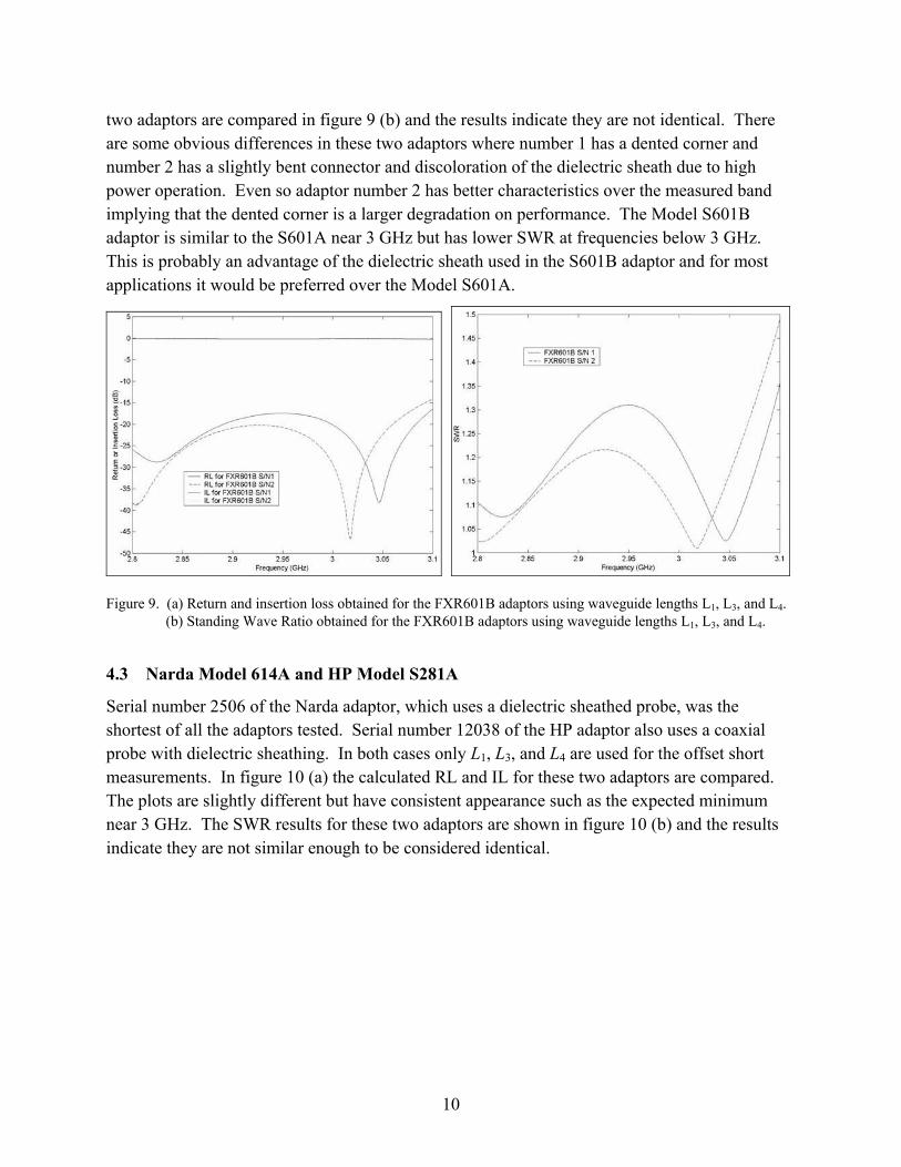
10
two adaptors are compared in figure 9 (b) and the results indicate they are not identical. There are some obvious differences in these two adaptors where number 1 has a dented corner and number 2 has a slightly bent connector and discoloration of the dielectric sheath due to high power operation. Even so adaptor number 2 has better characteristics over the measured band implying that the dented corner is a larger degradation on performance. The Model S601B adaptor is similar to the S601A near 3 GHz but has lower SWR at frequencies below 3 GHz. This is probably an advantage of the dielectric sheath used in the S601B adaptor and for most applications it would be preferred over the Model S601A.
Figure 9. (a) Return and insertion loss obtained for the FXR601B adaptors using waveguide lengths L1, L3, and L4. (b) Standing Wave Ratio obtained for the FXR601B adaptors using waveguide lengths L1, L3, and L4.
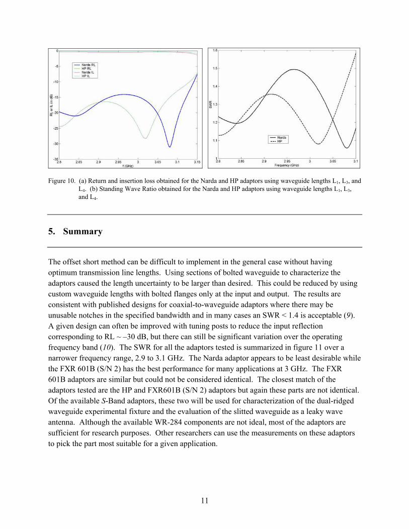
4.3 Narda Model 614A and HP Model S281A
Serial number 2506 of the Narda adaptor, which uses a dielectric sheathed probe, was the shortest of all the adaptors tested. Serial number 12038 of the HP adaptor also uses a coaxial probe with dielectric sheathing. In both cases only L1, L3, and L4 are used for the offset short measurements. In figure 10 (a) the calculated RL and IL for these two adaptors are compared. The plots are slightly different but have consistent appearance such as the expected minimum near 3 GHz. The SWR results for these two adaptors are shown in figure 10 (b) and the results indicate they are not similar enough to be considered identical.
11
Figure 10. (a) Return and insertion loss obtained for the Narda and HP adaptors using waveguide lengths L1, L3, and L4. (b) Standing Wave Ratio obtained for the Narda and HP adaptors using waveguide lengths L1, L3, and L4.
5. Summary
The offset short method can be difficult to implement in the general case without having optimum transmission line lengths. Using sections of bolted waveguide to characterize the adaptors caused the length uncertainty to be larger than desired. This could be reduced by using custom waveguide lengths with bolted flanges only at the input and output. The results are consistent with published designs for coaxial-to-waveguide adaptors where there may be unusable notches in the specified bandwidth and in many cases an SWR < 1.4 is acceptable (9). A given design can often be improved with tuning posts to reduce the input reflection corresponding to RL ~ –30 dB, but there can still be significant variation over the operating frequency band (10). The SWR for all the adaptors tested is summarized in figure 11 over a narrower frequency range, 2.9 to 3.1 GHz. The Narda adaptor appears to be least desirable while the FXR 601B (S/N 2) has the best performance for many applications at 3 GHz. The FXR 601B adaptors are similar but could not be considered identical. The closest match of the adaptors tested are the HP and FXR601B (S/N 2) adaptors but again these parts are not identical. Of the available S-Band adaptors, these two will be used for characterization of the dual-ridged waveguide experimental fixture and the evaluation of the slitted waveguide as a leaky wave antenna. Although the available WR-284 components are not ideal, most of the adaptors are sufficient for research purposes. Other researchers can use the measurements on these adaptors to pick the part most suitable for a given application.

12
Figure 11. Standing Wave Ratio obtained for microwave adaptors using waveguide lengths L1, L3, and L4.
13
6. References
1. Goldstone, L. O.; Oliner, A. A. Leaky-Wave Antennas I: Rectangular Waveguides. IRE Trans. Antennas Propagat. October 1959, AP-5, 307–319.
2. Coburn, W.; Wasylkiwskyj, W. Design Procedure for a Frequency Scanned Traveling Wave Antenna, Part I – Air-filled Waveguide; ARL-TR-791; U.S. Army Research Laboratory: Adelphi, MD, September 2001.
3. Coburn, W.; Wasylkiwskyj, W. Design Procedure for a Frequency Scanned Traveling Wave Antenna, Part II – Dielectric-Loaded Waveguide; ARL-TR-3132; U.S. Army Research Laboratory: Adelphi, MD, December 2003.
4. Pozar, D. M. Microwave Engineering; 2nd ed., John Wiley: New York, 1998.
5. Marcurvitz, N. ed., Waveguide Handbook; McGraw-Hill: New York, 1951.
6. Ramo, S.; Whinnery, J. R.; Van Duzer, T. Fields and Waves in Communication Electronics, 2nd ed., John Wiley: New York, 1984.
7. Saad, Theodore S. ed., Microwave Engineers’ Handbook – Vol I; Artech House: Dedham, Massachusetts, 1971.
8. Bialkowski, M. E. Analysis of a Coaxial-to-Waveguide Adaptor Incorporating a Dielectric Coated Probe. IEEE Microw. And Guided Wave Letters August 1991, 1 (8), 211–214.
9. Keam, R. B.; Williamson, A. G. Broadband Design of Coaxial Line/Rectangular Waveguide Probe Transition. IEE Proc.-Microw. Antenna Propag. February 1994, 141 (1), 53–58.
10. Bialkowski, M. E. Analysis of a Coaxial-to-Waveguide Adaptor Including a Discended Probe and a Tuning Post. IEEE Trans. Microw. Theory and Tech. February 1995, 43 (2), 344–349.
14
Distribution List
ADMNSTR DEFNS TECHL INFO CTR ATTN DTIC-OCP (ELECTRONIC COPY) 8725 JOHN J KINGMAN RD STE 0944 FT BELVOIR VA 22060-6218
DARPA ATTN IXO S WELBY 3701 N FAIRFAX DR ARLINGTON VA 22203-1714
OFC OF THE SECY OF DEFNS ATTN ODDRE (R&AT) THE PENTAGON WASHINGTON DC 20301-3080
US ARMY TRADOC BATTLE LAB INTEGRATION & TECHL DIRCTRT ATTN ATCD-B 10 WHISTLER LANE FT MONROE VA 23651-5850
DIR FOR MANPRINT OFC OF THE DEPUTY CHIEF OF STAFF FOR PRSNNL ATTN J HILLER THE PENTAGON RM 2C733 WASHINGTON DC 20301-0300
US MILITARY ACDMY MATHEMATICAL SCI CTR OF EXCELLENCE ATTN LTC T RUGENSTEIN THAYER HALL RM 226C WEST POINT NY 10996-1786
SMC/GPA 2420 VELA WAY STE 1866 EL SEGUNDO CA 90245-4659
US ARMY ARDEC ATTN AMSTA-AR-TD BLDG 1 PICATINNY ARSENAL NJ 07806-5000
US ARMY AVN & MIS CMND ATTN AMSMI-RD W C MCCORKLE REDSTONE ARSENAL AL 35898-5240
US ARMY INFO SYS ENGRG CMND ATTN AMSEL-IE-TD F JENIA FT HUACHUCA AZ 85613-5300
US ARMY NATICK RDEC ACTING TECHL DIR ATTN SBCN-TP P BRANDLER KANSAS STREET BLDG78 NATICK MA 01760-5056
US ARMY SIMULATION TRAIN & INSTRMNTN CMND ATTN AMSTI-CG M MACEDONIA 12350 RESEARCH PARKWAY ORLANDO FL 32826-3726
HICKS & ASSOC INC ATTN G SINGLEY III 1710 GOODRICH DR STE 1300 MCLEAN VA 22102
PALISADES INST FOR RSRCH SVC INC ATTN E CARR 1745 JEFFERSON DAVIS HWY STE 500 ARLINGTON VA 22202-3402

15
DIRECTOR US ARMY RSRCH LAB ATTN AMSRD-ARL-RO-D JCI CHANG ATTN AMSRD-ARL-RO-EN W D BACH PO BOX 12211 RESEARCH TRIANGLE PARK NC 27709
US ARMY RSRCH LAB ATTN AMSRD-ARL-D J M MILLER ATTN AMSRD-ARL-CI-IS MAIL & RECORDS MGMT ATTN AMSRD-ARL-CI-OK-T TECHL PUB (2 COPIES) ATTN AMSRD-ARL-CI-OK-TL TECHL LIB (2 COPIES) ATTN AMSRD-ARL-SE-RU W O COBURN ADELPHI MD 20783-1197