measurement process of mosfet device parameters...
TRANSCRIPT

Int. J. Communications, Network and System Sciences, 2011, 4, 590-600 doi:10.4236/ijcns.2011.49071 Published Online September 2011 (http://www.SciRP.org/journal/ijcns)
Copyright © 2011 SciRes. IJCNS
Measurement Process of MOSFET Device Parameters with VEE Pro Software for DP4T RF Switch
Viranjay M. Srivastava1, K. S. Yadav2, G. Singh1 1Department of Electronics and Communication Engineering,
Jaypee University of Information Technology, Solan, India 2VLSI Design Group, Central Electronics Engineering Research Institute (CEERI), Pilani, India
E-mail: [email protected] Received July 9, 2011; revised August 13, 2011; accepted August 26, 2011
Abstract To design a Double-Pole Four-Throw (DP4T) RF switch, measurement of device parameters is required. In this DP4T RF switch CMOS is a unit cell, so with a thin oxide layer of thickness 628 Å which is measured optically. Some of the material parameters were found by the curve drawn between Capacitance versus Voltage (C-V) and Capacitance versus Frequency (C-F) with the application of Visual Engineering Envi-ronment Programming (VEE Pro). To perform the measurement processing at a distance, from the hazardous room, we use VEE Pro software. In this research, to acquire a fine result for RF MOSFET, we vary the volt-age with minor increments and perform the measurements by vary the applying voltage from +5 V to –5 V and then back to +5 V again and then save this result in a data sheet with respect to temperature, voltage and frequency using this program. We have investigated the characteristics of RF MOSFET, which will be used for the wireless telecommunication systems. Keywords: Capacitance-Frequency Curve, Capacitance-Voltage Curve, DP4T Switch, LCR Meter, MOS
Device, Radio Frequency, RF Switch, Testing, VEE Pro, VLSI
1. Introduction To understand the capacitance-voltage and capacitance- frequency effect, we design a process to measure the characteristics curve at different frequencies. The fre-quency dependence occurs primarily in inversion. A cer-tain time is needed to generate the minority carriers in the inversion layer. Therefore, the thermal equilibrium is therefore not obtained immediately [1]. Since the minor-ity carriers within the inversion layer of an inverted MOS capacitor can move in response to a radio-frequency AC signal even though the total minority carrier charge is fixed at the value set by the DC bias. The resulting ca-pacitance is restricted to the case where minority-carrier trapping by defects in the inversion layer or at the inter-face does not significantly hinder the AC response of the minority carriers. Comparisons of this new result with only curve (not with formula) are discussed with the calculations of Sah and Pierret theorems [2].
The organization of this paper is as follows: Section 1 provides the introduction of VEE Pro, Antenna system, LCR Meter and capacitance-voltage and capacitance-
frequency effect. In the Section 2 we discussed the measurements process of device parameters. In the Sec-tion 3 results are discussed and finally Section 4 con-cludes the work. 1.1. Visual Engineering Environment
Programming (VEE Pro) Visual Engineering Environment Programming (VEE Pro) is a graphical programming environment optimized for use with electronic instruments. The simplest way to state its value is the phrase, “Better measurements faster”. Software prototyping is noticeably faster with VEE Pro than with the lower-level languages, and hundreds of powerful functions are available to help for analyze the measurement data [3]. The VEE programming environ-ment strongly supports electronic instrument and meas-urement tasks. For those early prototyping stages, VEE Pro provides simulated signal sources and displays. We design an experiment set-up with program flow and data processing without any external hardware. VEE Pro pro-vides an instrument manager and a dynamic input/output

V. M. SRIVASTAVA ET AL.
591
server to simplify the tasks of discovering, configuring, and managing external instruments. The VEE Pro sup-ports several types of instrument drivers and has the op-tion to choose the driver that best suits the preferences and/or the characteristics of an instrument. For those times when the instruments are not available, just press one button in the Instrument Manager of the program-ming to take a driver “off line” and continue to develop-ing the measurement [4-6].
Virtual instruments exist within the VEE Pro program whereas the real (actual) instruments are attached via special plug-in cards. Often, a separate card is required for each instrument. Instruments now coming online contain USB links that can go directly to a computer, and some have LAN connections which do not need any spe-cific cards. The VEE Pro test program controls [7]:
1) The virtual or actual instrument are connected via VEE Pro,
2) The parameters are to be monitored, 3) The data has to be processed, 4) The data are stored—as either raw data or processed
data, and 5) The data are processed for spreadsheets, reports,
and databases. 1.2. Antenna System In the wireless communication system, the signals from a subset of the antennas are processed at any time by the limited bandwidth of radio frequency (RF), which is available for the receiver. Hence, the transmitter needs to send pilots multiple times to enable the receiver to esti-mate the channel state of all the antennas and select the best subset. In the RF transceiver system, multiple an-tenna system circuitries are used to substitute conven-tional single antenna circuitry, which improves the transmission capability and reliability of the communica-tion systems. With the multiple antennas, data transfer rate is increased by the same factor as the numbers of antenna are used. Antenna selection system and switch-ing mechanism is essential to circumvent the uses of several RF chain associated with the various antennas [8,9].
Due to the single operating frequency, a simple switch has a limited data transfer rate. Therefore, a Double-Pole Double-Throw (DPDT) switch is designed to solve the problem and increase the data transfer rate “two times”. The DPDT switch has dual antenna and dual ports, one port for transmitting and the other for receiving, which is not sufficient for MIMO systems. Hence, DP4T switch is designed to enhance the switching performance of the MIMO applications. This DP4T switch can send or re-ceive two parallel data streams simultaneously means
data transfer rate increases “four times” [10-12]. 1.3. E4980A Precision L-C-R Meter Designed for measurement precision and ease of use, this Agilent family of LCR (Inductor, Capacitor, and Resistor) meter fits for both research and production applications. The LCR meter does not have all the sophisticated fea-tures as impedance analyzers. It offers excellent per-formance at an affordable cost. The arrangment for hea- ting system, RF MOS device and probe through which device and LCR meters are connected, as shown in Figure 1. The purpose of heating the device is to get accurate measurment of parameters due to the effect of charges in oxide layer [4]. The properties of LCR meter is as following [13],
1) Wide selection of frequency range from 20 Hz to 3 GHz (includes RF range).
2) Frequency list sweep for continuous testing at mul-tiple frequency points.
3) Used for general purpose testing of surface-mount components, leaded components and materials.
4) GPIB and handler interface for easy test automation in production environment.
5) It has 0.05% basic accuracy 6) Measurement parameters: impedance (Z), admit-
tance (Y), resistance (R), Inductance (L), capacitance (C), transconductance (X), magnetc field (B), quality factor (Q), DC resistance (Rdc), DC currnt (Idc), DC voltage (Vdc) 1.4. Capacitance-Voltage and
Capacitance-Frequency Characteristics The real importance of Capacitance-Voltage and Ca-pacitance-Frequency curve measurement techniques in RF MOS switch is that a large number of device pa-
Figure 1. Agilent E4980A LCR meter.
Copyright © 2011 SciRes. IJCNS

592 V. M. SRIVASTAVA ET AL.
rameters can be extracted from two simple curves: the high frequency (Radio frequency range) C-V curve and the quasi-static C-V curve. These parameters can provide critical device and process information which is useful for the decreasing MOS length technology. Here the purpose is to achieve a minimal work-function difference between the gate and the semiconductor, while main-taining the conductive properties of the gate. Based on the C-V characterization of a RF MOS capacitor with VEE Pro software, which resulted in flawed values of device parameters [11,12], mainly the substrate dopant concentration, on which most of the other parameters are based. The readings stored in excel sheet can be used for further processing and we can utilize this process for DP4T switch.
Capacitance-voltage (C-V) and Capacitance-frequency (C-F) measurement of MOS capacitors provides infor-mation about the structure, which is of direct interest when we evaluate a MOS process. For a capacitor formed of MOS device using Metal-silicon dioxide-silicon layers with an oxide thickness of 628 Å (measured optically), some of the material parameters were found from the curve drawn through VEE Pro software. To perform the measurement, process by a distance, from the hazardous room, we use the VEE Pro software in the BEL laboratory. In this paper, to find good result, vary the voltage with smaller increments and perform the measurements by varying the voltage from +5 V to –5 V and then back to +5 V again and then save this result in a data sheet with re-spect to temperature, voltage and frequency using this programming [14,15]. 2. Process for Measurements of Device
Parameters The real importance of capacitance-voltage curve (C-V) measurement techniques is a large number of device pa-rameters can be extracted from two apparently simple curves: high frequency (Radio frequency range) C-V curve and quasistatic C-V curve. These parameters pro-vide the critical device and process information. We can divide the parameters into three groups [16,17].
1) Includes typical MOS device parameters such as flatband voltage, threshold voltage.
2) Oxide charge parameters, includes interface trap charge density, mobile ion charge density, etc.
3) Consists of doping-related parameters. Also by using C-t data, carrier generation lifetime and
recombination lifetime can be extracted [18]. This re-search addresses the following parameters that can be extracted from a high-frequency C-V (RF-CV) curve:
1) Oxide thickness. 2) Flat band capacitance and flat band voltage.
3) Threshold voltage. 4) Calculating the metal-semiconductor work function
difference. To perform this experiment, for measurement of ca-
pacitances at different voltages, mainly for a predefined voltage range [7,19], we programmed, using the pro-gramming tools in VEE Pro software which is interface with the LCR meter as shown in Figure 1. Following steps are processed for the measurement of device pa-rameters.
Step 1: Fabrication of RF MOSFET Device Similar size MOS capacitors were fabricated on a 4
inch diameter and 800 μm thick n-type silicon wafer and the grown layers were characterized by C-V, C-F and sheet resistance measurements [20-22]. To fabricate metal-oxide-semiconductor, the silicon wafers were cl- eaned by following the standard cleaning procedure to remove insoluble organics and metallic contaminants. After that, a layer of oxide, approximately 650 Å thick, was grown on the silicon wafers using a dry oxidation process at 950˚C for 2 hour, with a pre-ramp and post-ramp of 800˚C with N2 (12) and O2 (32). For top layer we will use Aluminum due to its ease of processing, ability to reduce native SiO2, which is always present in silicon wafers, exposed to atmosphere and its low resis-tivity. About 2000 Å of Aluminium was then deposited over the oxide layer using the sputtering process [16,18].
Various techniques are used to increase the sputtering rates, use of magnetic field near the target to increase the generation of ions. Introduction of electrons by the use of an electron gun as a third electrode was also tried.
The fabricated capacitors electrically tested to charac-terize the material and to inspect the device performance. The variation of the capacitance (C) with gate voltage (VG) ranging from –5 to +5 Volts and the capacitance with frequency ranging from 10 KHz to 1.2 MHz of a 100 μm × 100 μm capacitor are shown in Figures 2-8, curves are taken before heating and after heating the MOS device.
For a relatively thick oxide (>600 Å), extracting the oxide thickness is fairly simple. The oxide capacitance (Cox) is the high-frequency capacitance when the device is biased for strong accumulation. In the strong accumu-lation region, the MOS capacitor (MOS-C) acts like a parallel plate capacitor and the oxide thickness is calcu-lated from Cox and the gate area using the following equation [23-25]:
oxox
ox
T AC
(1)
Here A is the gate area of metal (10–2 cm2), εox is 34.515*10–14 F-cm–1 and then Cox is oxide capacitance measured by C-V curve for Accumulation region = 5.202
Copyright © 2011 SciRes. IJCNS

V. M. SRIVASTAVA ET AL.
Copyright © 2011 SciRes. IJCNS
593
pF by Figure 2, So by calculation of above (1), the value of Tox comes 675 Å. However, the measured oxide thickness using the UV method was 628 Å. So the ca-pacitance measurement seems to be low thus giving a thickness value greater than the actual value.
Step 2: Programming for Readings Since for the measurement, first select the input range
of voltages at which curve for the capacitances at differ-ent voltage is required [17]. Procedure of this program-ming is shown in Figure 9. For this purpose the pro-gramming is done on basis that to set the no. of divisions, take the difference of maximum and minimum voltage (for voltage range), and divide them by the number of division, at which capacitances are to be measured. After that addition, this small division to the minimum voltage as in Figure 9, one by one, until we reach to maximum voltage, this is done in programming using loop bearing name “for count and division” as shown in Figure 9 and a switch is added (bearing block named “click for each reading”), by which two readings can be taken, one be-fore heating and other after heating, so that better per-formance can be observed. To set the frequency at which reading of capacitances are required (low frequency or quasistatic and high frequency or radio frequency) [2, 26-29] here is a block with name “frequency” is added.
This frequency can vary from 10 Hz to 1 MHz. For the frequency we have to write only the value of frequency. Figures 2 and 3 show the high-frequency (1 MHz) and low-frequency (10 KHz) C-V curve for n-type MOS.
As in Figure 9, the reading is taken at 1 MHz and it is written as 1 M. After setting the volage range and fre-quency, we can take the reading on excel sheet as well as on window of programme, Also the graph of capacitan-ces at these voltages and frequencies are drawn by using this programme on the graph sheet which are shown in Figures 2-8, before heating and after heating (reading and graphs) respectively. The purpose of heating the de-vice is to get accurate measurment of parameters [30,31].
The value of the capacitances is compared. If the cur- ves are within the limit as shown in Figure 4 (yellow coloured/solid line shows before heating curve and green coloured/dashed line shows after heating curve of ca-pacitance vs voltage), then MOS device is good for ap-plication, but if it is out of limit then device will not be used for further application. These limit can be given by the consumer, who will use these devices. By this pro-gramme from a remote place we can measure the cor-rectness of MOS devices. The obtained results can be saved in required format as in .doc or in .xls format as shown in Figure 10.
Figure 2. Main programming block of VEE Pro for the LCR meter.

594 V. M. SRIVASTAVA ET AL.
Figure 3. High-frequency (1 MHz) C-V curve for a n-type MOS.
Figure 4. Low-frequency (10 KHz) C-V curve for a n-type MOS.
Copyright © 2011 SciRes. IJCNS

V. M. SRIVASTAVA ET AL.
595
Figure 5. High-frequency (1MHz) C-V curve for a p-type before heating (1st data) & after heating (2nd data).
Figure 6. Curve for C-F at applied voltage = –5 V (before heating).
Copyright © 2011 SciRes. IJCNS
596 V. M. SRIVASTAVA ET AL.
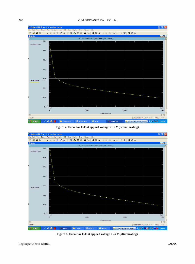
Figure 7. Curve for C-F at applied voltage = +5 V (before heating).
Figure 8. Curve for C-F at applied voltage = –5 V (after heating).
Copyright © 2011 SciRes. IJCNS

V. M. SRIVASTAVA ET AL.
597
Figure 9. Curve for C-F at applied voltage = +5 V (after heating).
Figure 10. Comparison of data of capacitances before heating and after heating on Excel sheet.
Copyright © 2011 SciRes. IJCNS

V. M. SRIVASTAVA ET AL.
Copyright © 2011 SciRes. IJCNS
598 3. Results By using the VEE Pro software with the above designed programming after storing data on excel sheet, parame-ters can be automatically calculated from test data at the end of the C-V and C-F test. The MOS capacitances with voltage or frequency curves have been extensively used for the determination of the surface states. A parallel displacement of the theoretical curve along the voltage axis would indicate the presence of fixed charges in the oxide, while any distortion of the shape of the experi-mental curve compared with the theory would indicate the presence of chargeable fast surface states at the ox-ide-semiconductor surface. We would see that the deter-mination of the surface states by using the constant ca-pacitance/voltage curve instead of the more exact non- constant capacitance/voltage curve introduces little error [2]. Since this represents the change between two ther-mal equilibrium situations, this capacitance should be measured while maintaining equilibrium conditions at all times. So there may be some error occurred.
At low frequencies the MOS structure is in thermal equilibrium under small signal ac excitation provided that minority carriers can respond to variations in the AC field to prevent energy loss [32-35]. The increase in ca-pacitance in inversion only occurs if the generation/re- combination of electrons can keep up with the applied ac signal. Capacitance meters generally employ a small ac signal superimposed upon the DC gate bias to measure the MOS capacitance. In practice, recombination/gen- eration rates are relatively slow so that the capacitance does not increase above a frequency of about 100 Hz for the Si-SiO2 [36,37]. In the presence of some additional reservoir of electrons, the low frequency behavior may be extended up to the MHz range. This is the case for a MOSFET where the reservoir is the source and drain n+ regions.
If both the gate bias VG and the small signal measuring voltage vary at a faster rate than may be allowed by re-combination/generation at the surface, then no inversion layer forms and the MOS device goes into deep depletion. In order to equate metal surface charge, the depletion region must widen to expose more ionized acceptors. Thus the capacitance decreases even further. The deple-tion region width is now larger than the depletion width saturation value [4]. 4. Conclusions We have demonstrated the method of automating photo-acoustic spectrometer through Agilent VEE Pro software with the designed program. The repeatability and reli-ability of the measurements are well tested by this auto-
mated instrument for thermal properties of glass and silicon wafer. Using the VEE Pro software with above programming to store data on Excel sheet, parameters of RF MOS switch as oxide thickness, flat band capacitance and flat band voltage, threshold voltage and metal- semiconductor work function difference can be auto-matically calculated from test data at the end of the C-V and C-F test, and then this calculated parameters can be automatically entered back into the data worksheet for record purpose.
In this experiment we also identified the improper contact of the probes with the wafer surface which is connected to LCR meter as the most probable cause of that along with the possibility of going unintentionally into deep depletion or having the equipment improperly calibrated. This can give erroneous result. This work can be used in future for measuring cleaning or sanitation of fabrication pipes as doping machine, oxidation chamber, furnaces and to calibrate the parameters in fabrication lab for any type of MOS devices or any other type of elec-tronic device [38,39]. Since the operating frequencies of the RF switches are in the order of GHz, therefore, it is useful for data link transmitter, radio transceiver switch, wireless local area network and other IEEE 802.11 in-dustrial applications including Wi-Fi system and high- energy radiotherapy applications, and analog to digital converters [40,41]. 5. References [1] V. M. Srivastava, K. S. Yadav and G. Singh, “Application
of VEE Pro Software for Measurement of MOS Device Parameters Using C-V Curve,” International Journal of Computer Applications, Vol. 1, No. 7, March 2010, pp. 43-46.
[2] J. R. Brews, “Error Analysis of High-Frequency MOS Capacitance Calculation,” Solid State Electronics, Vol. 17, No. 5, May 1974, pp. 447-456. doi:10.1016/0038-1101(74)90074-4
[3] Agilent Company, “Agilent VEE Pro User’s Guide,” Love-land, 2008.
[4] T. J. Mego, “Online C-V Doping Profile Measurement of Low Dose Ion Implant,” IEEE Transactions on Electron Devices, Vol. 27, No. 12, 1980, pp. 2268-1173. doi:10.1109/T-ED.1980.20263
[5] J. Zarębski and K. Górecki, “A Method of the Thermal Resistance Measurements of Semiconductor Devices with p-n Junction,” Journal of Measurement, Vol. 41, No. 3, April 2008, pp. 259-265. doi:10.1016/j.measurement.2006.11.009
[6] A. K. Sawhney and P. Sawhney, “A Course in Electrical and Electronic Measurements and Instrumentation,” Tata McGraw Hill Publications, New Delhi, 2004.
[7] K. Jeyadheepan, P. Palanichamy, P. Kalyanasundaram, M. Jayaprakasam, C. Sanjeeviraja and K. Ramachandran,

V. M. SRIVASTAVA ET AL.
599
“Automation of Photoacoustic Spectrometer Using VEE Pro Software,” Journal of Measurement, Vol. 43, No. 10, 2010, pp. 1336-1344. doi:10.1016/j.measurement.2010.07.011
[8] V. M. Srivastava, K. S. Yadav and G. Singh, “Analysis of Double Gate CMOS for Double-Pole Four-Throw RF Switch Design at 45-nm Technology,” Journal of Com-putational Electronics, Vol. 10, No. 1-2, June 2011, pp. 229-240. doi:10.1007/s10825-011-0359-6
[9] P. Mekanand and D. Eungdamorang, “DP4T CMOS Switch in a Transceiver of MIMO System,” Proceedings of 11th IEEE International Conference of Advanced Communication Technology, Gangwon-Do, 15-18 Febru-ary 2009, pp. 472-474.
[10] V. M. Srivastava, K. S. Yadav and G. Singh, “Design and Performance Analysis of Cylindrical Surrounding Dou-ble-Gate MOSFET for RF Switch,” Microelectronics Journal, Vol. 42, No. 10, October 2011, pp. 1124-1135. doi:10.1016/j.mejo.2011.07.003
[11] P. H. Woerlee, M. J. Knitel and A. J. Scholten, “RF CMOS Performance Trends,” IEEE Transactions on Electron Devices, Vol. 48, No. 8, 2001, pp. 1776-1782. doi:10.1109/16.936707
[12] V. M. Srivastava, K. S. Yadav and G. Singh, “Design and Performance Analysis of Double-Gate MOSFET over Single-Gate MOSFET for RF Switch,” Microelectronics Journal, Vol. 42, No. 3, March 2011, pp. 527-534. doi:10.1016/j.mejo.2010.12.007
[13] M. Popa and R. Ionel, “Virtual Instrumentation Applica-tion for System Identification,” Proceedings of IEEE In-strumentation and Measurement Technology Conference, Sorrento, 24-27 April 2006, pp. 842-846. doi:10.1109/IMTC.2006.328215
[14] J. Brews, “An Improved High-Frequency MOS Capaci-tance Formula,” Journal of Applied Physics, Vol. 45, No. 3, June 1974, pp. 1276-1279. doi:10.1063/1.1663401
[15] G. Panigrahi “Numerical Calculation of Low Frequency Capacitance/Voltage Curves of MOS Capacitor with Nonconstant Doping Profiles,” Electronics Letters, Vol. 9, No. 2, Jan 1973, pp. 43-45. doi:10.1049/el:19730030
[16] T. J. Mego, “Guidelines for Interpreting CV Data,” Solid State Technology, Vol. 33, No. 5, May 1990, pp. 159- 163.
[17] S. M. Sze, “Physics of Semiconductor Devices,” 2nd Edition, Wiley, New York, 1985.
[18] E. H. Nicollian and J. R. Brews, “MOS Physics and Technology,” Wiley, New York, 1982.
[19] Y. Cheng and M. Matloubian, “Frequency Dependent Resistive and Capacitive Components in RF MOSFETs,” IEEE Electron Device Letters, Vol. 22, No. 7, July 2001, pp. 333-335. doi:10.1109/55.930682
[20] N. Weste and D. Harris, “CMOS VLSI Design: A Cir-cuits and Systems Perspective,” 3rd Edition, Pearson Ad-dison Wesley, Boston, 2005.
[21] M. Fragopoulou, S. Siskos, M. Manolopoulou, M. Zamani and G. Sarrabayrouse, “Thermal Neutron Dosimetry Us-
ing MOSFET Dosemeters,” Journal of Radiation Meas- urement, Vol. 44, No. 9-10, 2009, pp. 1006- 1008.
[22] S. K. Ghandhi, “VLSI Fabrication Principles: Silicon and Gallium Arsenide,” 2nd Edition, Wiley, New Delhi, 2004.
[23] V. M. Srivastava, K. S. Yadav and G. Singh, “Measurement of Oxide Thickness for MOS Devices, Using Simulation of SUPREM Simulator,”International Journal of Computer Applications, Vol. 1, No. 6, March 2010, pp. 66-70.
[24] A. Srivastava, P. Sarkar and C. K. Sarkar, “Study of Gate Dielectric Permittivity Variation with Different Equiva-lent Oxide Thickness on Channel Engineered Deep Sub- Micrometer N-MOSFET Device for Mixed Signal Ap-plications,” Microelectronics Reliability, Vol. 49, No. 4, April 2009, pp. 365-370. doi:10.1016/j.microrel.2008.11.008
[25] J. He, X. Zhang and Y. Y. Wang, “Modeling of MOSFET Surface Capacitance Behavior under Non-equilibrium,” IEEE Solid State Electronics, Vol. 50, No. 2, 2006, pp. 259-262. doi:10.1016/j.sse.2005.12.008
[26] T. H. Lee, “The Design of CMOS Radio Frequency Inte-grated Circuits,” 2nd Edition, Cambridge University Press, Cambridge, 2004.
[27] R. Biberger, G. Benstetter, H. Goebel and A. Hofer, “In-termittent-Contact Capacitance Spectroscopy—A New Method for Determining C-V Curves with Sub-Micron Lateral Resolution,” Journal of Microelectronics Reliabil-ity, Vol. 50, No. 9-11, 2010, pp. 1511-1513. doi:10.1016/j.microrel.2010.07.052
[28] S. Kang and Y. Leblebichi, “CMOS Digital Integrated Circuits Analysis and Design,” 3rd Edition, McGraw-Hill, New York, 2002.
[29] V. M. Srivastava, K. S. Yadav and G. Singh, “Designing Parameters for RF CMOS Cells,”Circuits and Systems, Vol. 1, No. 2, 2010, pp. 49-53. doi:10.4236/cs.2010.12008
[30] G. K. Yeap and F. N. Najm, “Low Power VLSI Design and Technology,” Pearson Addison Wesley, 1st Edition, Boston, 2008.
[31] J. P. Xu, X. Xiao and P. T. Lai, “A Carrier-Mobility Model for High-K Gate-Dielectric Ge Mosfets with Metal Gate Electrode,” Microelectronics Reliability, Vol. 50, No. 8, 2010, pp. 1081-1086. doi:10.1016/j.microrel.2010.04.016
[32] S. H. Lee, C. S. Kim and H. K. Yu, “A Small Signal RF Model and Its Parameter Extraction for Substrate Effects in RF MOSFETs,” IEEE Transactions on Electron De-vices, Vol. 48, No. 7, July 2001, pp. 1374-1379. doi:10.1109/16.930654
[33] T. Sokollik, “Plasma Physics,” Investigations of Field Dynamics in Laser Plasmas with Proton Imaging, Vol. 1, 2011, pp. 17-24. doi:10.1007/978-3-642-15040-1_3
[34] G. Katti, M. Stucchi, K. Meyer and W. Dehaene, “Elec-trical Modeling and Characterization of Through Silicon via for Three-Dimensional ICs,” IEEE Transactions on Electron Devices, Vol. 57, No. 1, 2010, pp. 256-262. doi:10.1109/TED.2009.2034508
Copyright © 2011 SciRes. IJCNS

V. M. SRIVASTAVA ET AL.
Copyright © 2011 SciRes. IJCNS
600
[35] G. Gildenblat, Z. Zhu and C. C. McAndrew, “Surface Potential Equation for Bulk MOSFET,” IEEE Solid State Electronics, Vol. 53, No. 1, 2009, pp. 11-13. doi:10.1016/j.sse.2008.09.007
[36] V. Sverdlov, “Scaling, Power Consumption, and Mobility Enhancement Techniques,” In: S. Selberherr, Ed., Strain Induced Effects in Advanced MOSFET, Computational Microelectronics, 2011, pp. 5-22. doi:10.1007/978-3-7091-0382-1_2
[37] Y. S. Lin, S. S. Lu, T. S. Lee and H. B. Liang, “Charac-terization and Modeling of Small Signal Substrate Resis-tance Effect in RF CMOS,” Proceedings of IEEE MTT-S Digest, Seattle, 2-7 June 2002, pp. 161-164.
[38] V. M. Srivastava, K. S. Yadav and G. Singh, “Perform- ance of Double-Pole Four-Throw Double-Gate RF CMOS Switch in 45 nm Technology,” International Journal of
Wireless Engineering and Technology, Vol. 1, No. 2, 2010, pp. 47-54. doi:10.4236/wet.2010.12008
[39] R. Tamer and K. Roy, “Analysis of Options in Dou-ble-Gate MOS Technology: A Circuit Perspective,” IEEE Transaction on Electron Devices, Vol. 54, No. 12, 2007, pp. 3361-3368. doi:10.1109/TED.2007.909057
[40] T. Cheung, P. K. N. Yu and M. J. Butson, “Low-Dose Measurement with a MOSFET in High-Energy Radio- therapy Applications,” Journal of Radiation Measure- ment, Vol. 39, No. 1, 2005, pp. 91-94.
[41] E. Allier, G. Sicard, L. Fesquet and M. Renaudin, “Asynchronous Level Crossing Analog to Digital Con- verters,” Journal of Measurement, Vol. 37, No. 4, June 2005, pp. 296-309. doi:10.1016/j.measurement.2005.03.002