mechanical properties of nanowires and nanobelts m properties of nanowires and nanobelts zhong lin...
TRANSCRIPT

Mechanical Properties of Nanowires and Nanobelts
Zhong Lin WangGeorgia Institute of Technology Atlanta Georgia USA
INTRODUCTION
Because of the high size and structure selectivity of
nanomaterials their physical properties could be quite
diverse depending on their atomic-scale structure size
and chemistry[1] To maintain and utilize the basic and
technological advantages offered by the size specificity
and selectivity of the nanomaterials there are three key
challenges that we need to overcome for the future tech-
nological applications of nanomaterials First synthesis
of size morphology and structurally controlled nanoma-
terials which are likely to have the precisely designed
and controlled properties Secondly novel techniques for
characterizing the properties of individual nanostructures
and their collective properties[2] This is essential for
understanding the characteristics of the nanostructures
Finally integration of nanomaterials with the existing
technology is the most important step for their applications
especially in nanoscale electronics and optoelectronics
Characterizing the mechanical properties of individual
nanotubesnanowiresnanobelt [called one-dimensional (1-
D) nanostructure] is a challenge to many existing testing
and measuring techniques because of the following
constrains First the size (diameter and length) is rather
small prohibiting the applications of the well-established
testing techniques Tensile and creep testing require that
the size of the sample be sufficiently large to be clamped
rigidly by the sample holder without sliding This is im-
possible for 1-D nanomaterials using conventional means
Secondly the small size of the nanostructure makes their
manipulation rather difficult and specialized techniques
are needed for picking up and installing individual
nanostructure Therefore new methods and methodologies
must be developed to quantify the properties of individual
nanostructure The objective of this chapter is to introduce
the theory and techniques that have developed for char-
acterizing the mechanical properties of individual nano-
tubesnanowiresnanobelt using in situ transmission elec-
tron microscopy (TEM)
DYNAMIC BENDING MODULUS BYELECTRIC FIELD-INDUCEDMECHANICAL RESONANCE
The main challenge for characterizing the mechanical
behavior of a single nanostructure is its ultrasmall size that
prohibits the application of conventional techniques We
first have to see the nanostructure and then measure its
properties TEM is a powerful tool for characterizing the
atomic-scale structures of solid materials A modern TEM
is a versatile machine that not only can provide a real
space resolution better than 02 nm but also can give a
quantitative chemical and electronic analysis from a
region as small as 1 nm It is feasible to receive a full
structure characterization from TEM A powerful and
unique approach could be developed if we can integrate
the structural information of a nanostructure provided by
TEM with the properties measured in situ from the same
nanostructure[3ndash5] This is a powerful technique that not
only can provide the properties of an individual nanotube
but also can give the structure of the nanotube through
electron imaging and diffraction providing an ideal
technique for understanding the propertyndashstructure rela-
tionship The objective of this section is to introduce this
technique and its applications
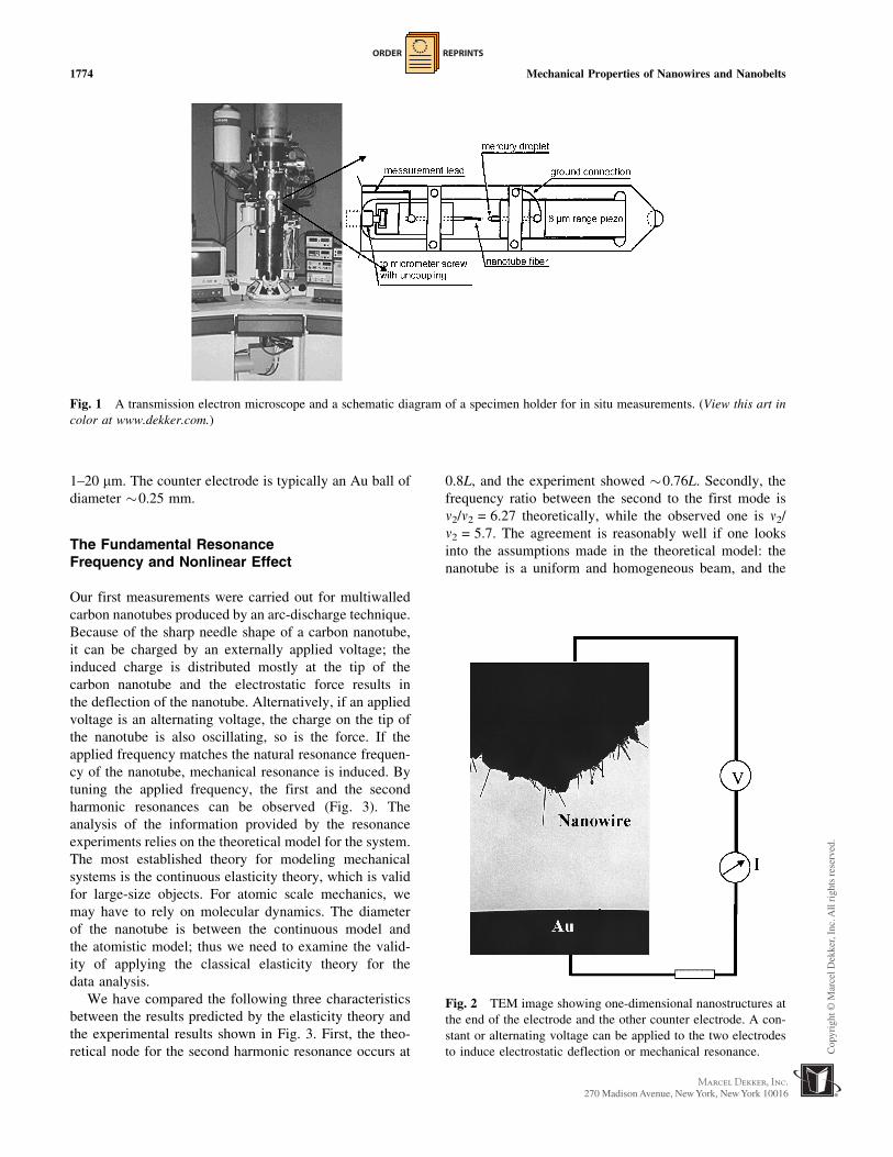
Experimental Method
To carry out the property measurement of a 1-D
nanostructure a specimen holder for a TEM was built
for applying a voltage across a 1-D nanostructure and its
counter electrode (Fig 1)[46] In the area that is loading
specimen in conventional TEM an electromechanical
system is built that allows not only the lateral movement
of the tip but also applying a voltage across the 1-D
nanostructure with the counter electrode This setup is
similar to the integration of scanning probe technique with
TEM The static and dynamic properties of the 1-D
nanostructures can be obtained by applying a controllable
static and alternating electric field The microstructure of
the measured object can be fully characterized by electron
imaging diffraction and chemical analysis techniques
The 1-D nanostructure to be used for property
measurements is directly imaged under TEM (Fig 2)
and electron diffraction patterns and images can be
recorded from the 1-D nanostructure The information
provided by TEM directly reveals both the surface and the
intrinsic structure of the 1-D nanostructure This is a
unique advantage over the SPM techniques The distance
from the 1-D nanostructure to the counter electrode is
controllable The typical dimensions of the 1-D nano-
structures are 5ndash100 nm in diameterwidth and lengths of
Dekker Encyclopedia of Nanoscience and Nanotechnology 1773
DOI 101081E-ENN 120013387
Copyright D 2004 by Marcel Dekker Inc All rights reserved
M
ORDER REPRINTS
1ndash20 mm The counter electrode is typically an Au ball of
diameter 025 mm
The Fundamental ResonanceFrequency and Nonlinear Effect
Our first measurements were carried out for multiwalled
carbon nanotubes produced by an arc-discharge technique
Because of the sharp needle shape of a carbon nanotube
it can be charged by an externally applied voltage the
induced charge is distributed mostly at the tip of the
carbon nanotube and the electrostatic force results in
the deflection of the nanotube Alternatively if an applied
voltage is an alternating voltage the charge on the tip of
the nanotube is also oscillating so is the force If the
applied frequency matches the natural resonance frequen-
cy of the nanotube mechanical resonance is induced By
tuning the applied frequency the first and the second
harmonic resonances can be observed (Fig 3) The
analysis of the information provided by the resonance
experiments relies on the theoretical model for the system
The most established theory for modeling mechanical
systems is the continuous elasticity theory which is valid
for large-size objects For atomic scale mechanics we
may have to rely on molecular dynamics The diameter
of the nanotube is between the continuous model and
the atomistic model thus we need to examine the valid-
ity of applying the classical elasticity theory for the
data analysis
We have compared the following three characteristics
between the results predicted by the elasticity theory and
the experimental results shown in Fig 3 First the theo-
retical node for the second harmonic resonance occurs at
08L and the experiment showed 076L Secondly the
frequency ratio between the second to the first mode is
n2n2 = 627 theoretically while the observed one is n2
n2 = 57 The agreement is reasonably well if one looks
into the assumptions made in the theoretical model the
nanotube is a uniform and homogeneous beam and the
Fig 2 TEM image showing one-dimensional nanostructures at
the end of the electrode and the other counter electrode A con-
stant or alternating voltage can be applied to the two electrodes
to induce electrostatic deflection or mechanical resonance
Fig 1 A transmission electron microscope and a schematic diagram of a specimen holder for in situ measurements (View this art in
color at wwwdekkercom)
1774 Mechanical Properties of Nanowires and Nanobelts
ORDER REPRINTS
root of the clamping side is rigid The latter however may
not be realistic in practical experiment Finally the shape
of the nanotube during resonance has been compared
quantitatively with the shape calculated by the elasticity
theory and the agreement is excellent Therefore we can
still use the elasticity theory for the data analysis
If the nanotube is approximated as a uniform solid bar
with one end fixed on a substrate from classical elasticity
theory the resonance frequency is given by[7]
ni frac14 b2i
8p1
L2
ffiffiffiffiffiffiffiffiffiffiffiffiffiffiffiffiffiffiffiffiffiffiffiffiffiffiffiffiffiethD2 thorn D2
i THORNEB
r
seth1THORN
where D is the tube outer diameter Di the inner diameter
L the length r the density and Eb the bending modulus It
must be pointed out that the bending modulus is different
from Youngrsquos modulus because bending modulus de-
pends on the geometrical shape of the object The reso-
nance frequency is nanotube selective and it is a specific
value of a nanotube
The correlation between the applied frequency and the
resonance frequency of the nanotube is not trivial From
Fig 2 we know that there are some electrostatic charges
built on the tip of the carbon nanotube With consideration
of the difference between the surface work functions
between the carbon nanotube and the counter electrode
(Au) a static charge exists even when the applied volt-
age is withdrawn Therefore under an applied field the
induced charge on the carbon nanotube can be repre-
sented by Q = Qo+aVocosot where Qo represents the
charge on the tip to balance the difference in surface
work functions a is a geometrical factor and Vo is the
amplitude of the applied voltage The force acting on the
carbon nanotube is
F frac14 bethQo thorn aVo cosotTHORNVo cosot
frac14 abV2o=2 thorn bQoVo cosot thorn abV2
o=2 cos 2ot eth2THORN
where b is a proportional constant Thus resonance can be
induced at o and 2o at vibration amplitudes proportional
to Vo and Vo2 respectively The former is a linear term in
which the resonance frequency equals to the applied
frequency while the latter is a nonlinear term and the
resonance frequency is twice of the applied frequency In
practical experiments the linear and nonlinear terms can
be distinguished by observing the dependence of the
vibration amplitude on the magnitude of the voltage Vo
This is an important process to ensure the detection of the
linear term
Another factor that one needs to consider is to iden-
tify the true fundamental resonance frequency From
Eq 1 the frequency ratio between the first two modes
is 627 In practice if resonance occurs at o resonance
could occur also at 2o which is the double harmonic
To identify the fundamental frequency one needs to
examine the resonance at a frequency that is half or close
to half of the observed resonance frequency if no reso-
nance occurs the observed frequency is the true funda-
mental frequency
The diameters of the tube can be directly determined
from TEM images at a high accuracy The determination
Fig 3 A selected carbon nanotube at (a) stationary (b) the first
harmonic resonance (n1 = 121 MHz) and (c) the second har-
monic resonance (n2 = 506 MHz) (d) The traces of a uniform
one-end fixed elastic beam at the first two resonance modes as
predicted by the continuous elasticity theory
Mechanical Properties of Nanowires and Nanobelts 1775
M
ORDER REPRINTS
of length has to consider the 2-D projection effect of the
tube It is essential to tilt the tube and to catch its
maximum length in TEM which is likely to be the true
length This requires a TEM that gives a tilting angle as
large as plusmn60 Also the operation voltage of the TEM is
important to minimize radiation damage The 100-kV
TEM used in our experiments showed almost no detect-
able damage to a carbon nanotube while a 200-kV
electron could quickly damage a nanotube The threshold
for radiation damage of carbon nanotubes is 150 kV
To trace the sensitivity of resonance frequency on
beam illumination and radiation damage at 100 kV a
carbon nanotube was resonanced for more than 30 min
The resonance frequency showed an increase of 14
over the entire period of experiment but no dependence
on the electron dose was found The FWHM for the
resonance peak was measured to be Dnn = 06 in a
vacuum of 104ndash105 Torr A slight increase in the
resonance frequency could be related to the change of
carbon structure under the electron beam but such an
effect has a negligible effect on the measurement of the
bending modulus
The Youngrsquos modulus is a quantity that is defined
to characterize the interatomic interaction force and it
is the double differential of the bonding energy curve
between the two atoms The ideal case is that it is an
intrinsic property at the atomic level and is independent
of the sample geometry For the nanotube case the bend-
ing of a nanotube is determined not only by the Youngrsquos
modulus but also by the geometrical shape of the nano-
tube such as the wall thickness and tube diameter What
we have measured by the in situ TEM experiments is the
bending modulus Fig 4 shows a group of experimentally
measured bending modulus of multiwalled carbon nano-
tubes It is apparent that the smaller-size nanotubes have
a bending modulus approaching the Youngrsquos modulus
while the modulus for the larger-size ones is much
smaller This size-dependent property is related to the
elastic deformation of the carbon nanotubes
To explore the intrinsic meaning of the measured Dnn1
value we consider a 1-D harmonic oscillator with an
intrinsic resonance frequency n1 If a viscosity (or friction)
force is acting on the particle and the force is proportional
to the instantaneous speed of the particle the damping of
the vibration amplitude is given by exp( tt0) where t0 is
the life decay constant of the oscillator This decay
constant is related to Dnn1 by Dnn11 by
t0 frac14 frac12ethDn=n1THORNpn1=17321 eth3THORN
For Dnn1 = 065 n1 = 10 MHz the lifetime is t0 = 85
msec From the definition of t0 the viscosityfriction
coefficient Z = 2Mt0 where M is the mass of the particle
thus the time decay constant depends mainly on the
viscosity coefficient of the nanotube in vacuum (104
Torr) under which the measurement was made and it
is almost independent of the intrinsic structure of the
carbon nanotube This agrees with our experimental ob-
servation and Eq 1 can also be used to explain the larger
value of Dnn1 obtained in air than that in vacuum given
that the atmosphere should have a higher viscosity
(friction) coefficient
Theoretical investigation by Liu et al[8] suggests that
the Eq 1 used for the analysis is based on the linear
analysis which is valid for a small amplitude of vibration
for large vibration amplitude the nonlinear analysis may
have to be used Based on the nonlinear elasticity theory
they have successfully explained the rippling effect
observed experimentally by Wang et al[4] In practical
experiments the resonance frequency shows no drift as
the vibration increases to as large as 30 suggesting that
the frequency measured can still be quantified using the
linear analysis
BENDING MODULUS OFCOMPOSITE NANOWIRES
The technique demonstrated for carbon nanotubes applies
to any nanowire shape object regardless of its conductiv-
ity[9] Here we use composite silicon carbidendashsilica
nanowires synthesized by a solidndashvapor process as an
example The as-synthesized materials are grouped into
three basic nanowire structures pure SiOx nanowires
coaxially SiOx sheathed b-SiC nanowires and biaxial b-
SiCndashSiOx nanowires Fig 5 depicts the TEM images of
the nanowires and their cross-section images showing the
coaxial and biaxial structures The nanowires are uniform
with a diameter of 50ndash80 nm and a length that can be as
Fig 4 Bending modulus of the multiwalled carbon nanotube
produced by arc-discharge as a function of the outer diameter of the
nanotube The inner diameter of the nanotubes is 5 nm inde-
pendent of the outer diameter The FWHM of the resonance peak
is inserted (View this art in color at wwwdekkercom)
1776 Mechanical Properties of Nanowires and Nanobelts
ORDER REPRINTS
long as 100 mm The coaxial SiCndashSiOx nanowires have
been extensively studied and have a h111i growth
direction with a high density of twins and stacking faults
perpendicular to the growth direction
For a beam with one end hinged and the other free the
resonance frequency is given by[7]
n0 frac14 ethb2=2pTHORNethEI=mTHORN1=2=L2 eth4THORN
where no is the fundamental resonance frequency
b = 1875 EI is the flexural rigidity (or bending stiffness)
E is the Youngrsquos modulus I is the moment of inertia about
a particular axis of the rod L is the length of the beam and
m is its mass per unit length For a uniform solid beam
with a coaxial cable structured nanowire whose core
material density is rc and diameter is Dc and a sheath
material density that is rs with outer diameter Ds the
average density of the nanowire is given by
re frac14 rcethD2c=D2
s THORN thorn rseth1 D2c=D2
s THORN eth5THORN
The effective Youngrsquos modulus of the composite nano-
wire Eeff is
Eeff frac14 refrac128pf0L2=b2Ds2 eth6THORN
The bending modulus for the coaxial cable structured
SiCndashSiOx nanowires results in combination from SiC and
SiOx where the contribution from the sheath layer of SiOx
is more than that from the SiC core because of its larger
flexural rigidity (or bending stiffness) The bending
modulus increases as the diameter of the nanowire
increases (Table 1) consistent with the theoretically
expected values of Eeff = aESiC +(1a)ESilica where
a = (DcDs)4 The data match well to the calculated values
for larger diameter nanowires
From the cross-sectional TEM image of a biaxially
structured nanowire the outermost contour of the cross
section of the nanowire can be approximated to be
elliptical Thus the effective Youngrsquos modulus of the
nanowire can be calculated using Eq 6 with the
introduction of an effective moment of inertia and density
For an elliptical cross section of half long-axis a and
half short-axis b the moments of inertia are Ix = pab34
and Iy = pba34 where a and b can be calculated from
the widths of the composite nanowire With considera-
tion of the equal probability of resonance with respect
to the x and y axes the effective moment of inertia
introduced in the calculation is taken to be approximately
I = (Ix+ Iy)2 and the density per unit length is meff =
Table 1 Measured Youngrsquos modulus of coaxial cable structured SiCndashSiOx nanowires (SiC is the core and silica is the sheath)
(rSilica = 22103 kgm3 rSiC = 32103 kgm3) The Youngrsquos modulii of the bulk materials are ESiC = 466 GPa and ESilica = 73 GPa
Ds (nm)
(plusmn2 nm)
Dc (nm)
(plusmn1 nm)
L (mmm)
(plusmn02 mmm) fo (MHz)
Eeff (GPa)
experimental
Eeff (GPa)
theoretical
51 125 68 0693 46plusmn90 73
74 26 73 0953 56plusmn92 78
83 33 72 1044 52plusmn82 82
132 48 135 0588 78plusmn70 79
190 105 190 0419 81plusmn51 109
Fig 5 (ab) TEM images of the coaxial and biaxial structured
SiCndashSiOx nanowires and (cd) the cross-sectional TEM
images respectively
Mechanical Properties of Nanowires and Nanobelts 1777
M
ORDER REPRINTS
ASiCrSiC+ASilicarSilica where ASiC and ASilica are the cross
sectional areas of the SiC and SiOx sides respectively
The experimentally measured Youngrsquos modulus is given
in Table 2
BENDING MODULUS OF OXIDE NANOBELTS
NanobeltsmdashStructurallyControlled Nanowires
In the literature there are a few names being used for
describing 1-D elongated structures such as nanorod
nanowire nanoribbon nanofiber and nanobelts When we
named the nanostructures to be lsquolsquonanobeltsrsquorsquo[10] we mean
that the nanostructure has specific growth direction the
topbottom surfaces and side surfaces are well-defined
crystallographic facets The requirements for nanowires
are less restrictive than for nanobelts because a wire has a
specific growth direction but its side surfaces may not be
well defined and its cross section may not be uniform nor
have a specific shape Therefore we believe that nano-
belts are more structurally controlled objects than
nanowires or simply a nanobelt is a nanowire that has
well-defined side surfaces It is well known that the
physical property of a carbon nanotube is determined by
the helical angle at which the graphite layer was rolled up
It is expected that for thin nanobelts and nanowires their
physical and chemical properties will depend on the
nature of the side surfaces
The most typical nanobelt is ZnO (Fig 6a) which has a
distinct cross section from the nanotubes or nanowires[10]
Each nanobelt has a uniform width along its entire length
and the typical widths of the nanobelts are in the range
of 50 to 300 nm A ripple-like contrast appearing in the
TEM image is due to the strain resulting from the bending
of the belt High-resolution TEM (HRTEM) and electron
diffraction studies show that the ZnO nanobelts are
structurally uniform single crystalline and dislocation
free (Fig 6b)
There are a few kinds of nanobelts that have been
reported in the literature Table 3 summarizes the nanobelt
structures of function oxides[10ndash14] Each type of nano-
belts is defined by its crystallographic structure the
growth direction top surfaces and side surfaces Some
of the materials can grow along two directions but they
can be controlled experimentally Although these mate-
rials belong to different crystallographic families they
do have a common faceted structure which is the nano-
belt structure In addition nanobelts of Cu(OH)2[15]
MoO3[1617] MgO[1819] and CuO[20]
Table 2 Measured Youngrsquos modulus of biaxially structured SiCndashSiOx nanowires Dwire and DSiC are
the widths across the entire nanowire and across the SiC subnanowire respectively
Dwire (nm)
(plusmn2 nm)
DSiC (nm)
(plusmn1 nm)
L (Mm)
(plusmn02 Mm) fo (MHz)
Eeff (GPa)
experimental
58 24 43 1833 54plusmn241
70 36 79 0629 53plusmn84
83 41 43 2707 61plusmn138
92 47 57 1750 64plusmn143
Fig 6 (a) TEM image of ZnO nanobelts synthesized by a solidndashvapor phase technique (b) High-resolution TEM image of a ZnO
nanobelt with incident electron beam direction along frac122110 The nanobelt grows along [0001] with topbottom surfaces eth2110THORN and side
surfaces eth0110THORN
1778 Mechanical Properties of Nanowires and Nanobelts
ORDER REPRINTS
Dual-Mode Resonance of Nanobelts
Because of the mirror symmetry and rectangular cross
section of the nanobelt (Fig 7a) there are two distinct
fundamental resonance frequencies corresponding to the
vibration in the thickness and width directions which are
given from the classical elasticity theory as[21]
nx frac14 b21T
4pL2
ffiffiffiffiffiffiEx
3r
seth7THORN
ny frac14 b21W
4pL2
ffiffiffiffiffiffiEy
3r
seth8THORN
where b1 = 1875 Ex and Ey are the bending modulus
if the vibration is along the x axis (thickness direction)
and y direction (width direction) respectively r is the
density L is the length W is the width and T is the
thickness of the nanobelt The two modes are decoupled
and they can be observed separately in experiments
Changing the frequency of the applied voltage we
found two fundamental frequencies in two orthogonal
directions transverse to the nanobelt[21] Fig 7c and d
shows the harmonic resonance with the vibration planes
nearly perpendicular and parallel to the viewing direction
respectively For calculating the bending modulus it is
critical to accurately measure the fundamental resonance
frequency (n1) and the dimensional sizes (L and T and W )
of the investigated ZnO nanobelts To determine n1 we
have checked the stability of the resonance frequency to
ensure that one end of the nanobelt is tightly fixed and the
resonant excitation has been carefully checked around the
half value of the resonance frequency
Fig 7 A selected ZnO nanobelt at (ab) stationary (c) the first harmonic resonance in the x direction nx1 =622 kHz and (d) the first
harmonic resonance in the y direction ny1 =691 kHz (e) An enlarged image of the nanobelt and its electron diffraction pattern (inset)
The projected shape of the nanobelt is apparent (f) The FWHM of the resonance peak measured from another ZnO nanobelt The
resonance occurs at 2309 kHz
Table 3 Crystallographic geometry of functional oxide nanobelts
Nanobelt Crystal structure Growth direction Top surface Side surface
ZnO Wurtzite [0001] or frac120110 plusmneth2110THORN or plusmneth2110THORN plusmneth0110THORN or plusmn(0001)
Ga2O3 Monoclinic [001] or [010] plusmn(100) or plusmn(100) plusmn(010) or plusmneth101THORNt-SnO2 Rutile [101] plusmneth101THORN plusmn(010)
o-SnO2 wire Orthorhombic [010] plusmn(100) plusmn(001)
In2O3 C-Rare earth [001] plusmn(100) plusmn(010)
CdO NaCl [001] plusmn(100) plusmn(010)
PbO2 Rutile [010] plusmn(201) plusmneth101THORN
Mechanical Properties of Nanowires and Nanobelts 1779
M
ORDER REPRINTS
ZnO nanobelts can be used as a force sensor Fig 8a
shows a selected ZnO nanobelt with a hooked end which
is equivalent to a cantilever with an integrated tip Be-
cause of the two transverse vibration modes of the
nanobelt resonance along two orthogonal directions has
been observed (Fig 8b and c) The two resonance modes
just correspond to the two modes of the tip operation
when the nanobelt-base cantilever is used as a force
sensor one is the tapping mode and the other is the
noncontact mode Thus the force sensor fabricated using
the ZnO nanobelts is versatile for applications on hard and
soft surfaces
Bending Modulus of Nanobelt
The geometrical parameters are the key for derivation of
the mechanical property from the measured resonance
frequencies The specimen holder is rotated about its axis
so that the nanobelt is aligned perpendicular to the
electron beam thus the real length (L) of the nanobelt can
be obtained The normal direction of the wide facet of the
nanobelt could be firstly determined by electron diffrac-
tion pattern which was frac122110 for the ZnO nanobelt Then
the nanobelt was tilted from its normal direction by
rotating the specimen holder and the tilting direction and
angle were determined by the corresponding electron
diffraction pattern As shown in the inset of Fig 7e the
electron beam direction is frac121100 The angle between
frac121100 and frac122110 is 30 ie the normal direction of the
wide facet of this nanobelt is 30 tilted from the direction
of the electron beam Using the projected dimension
measured from the TEM image (Fig 7e) the geometrical
parameters of this nanobelt are determined to be W = 28
nm and T = 19 nm Based on the experimentally measured
data the bending modulus of the ZnO nanobelts is
calculated using Eqs 7 and 8 The experimental results are
summarized in Table 4[21] The bending modulus of the
ZnO nanobelts was 52 GPa This value represents the
modulus that includes the scaling effect and geometrical
shape and it cannot be directly compared to the Youngrsquos
modulus of ZnO (c33 = 210 GPa c13 = 104 GPa)[22]
because the shape of the nanobelt and the anisotropic
structure of ZnO are convoluted in the measurement The
bending modulus measured by the resonance technique
however has excellent agreement with the elastic modu-
lus measured by nanoindentation for the same type of
nanobelts[23]
Although nanobelts of different sizes may have a slight
difference in bending modulus there is no obvious
difference if the calculation was done using either Eq 7
or Eq 8 The ratio of two fundamental frequencies ny1
nx1 is consistent with the aspect ratio WT as expected
from Eqs 7 and 8 because there is no significant dif-
ference between Ex and Ey
The resonance technique demonstrated here is very
sensitive to the structure of a nanowire Fig 9a and b
shows a silicon nanowire that has a Au tip but the Au
Fig 8 A selected ZnO nanobelt with a hooked end at (a)
stationary (b) resonance at 731 kHz in the plane almost parallel
to the viewing direction and (c) resonance at 474 kHz in the
place closely perpendicular to the viewing direction
Table 4 Bending modulus of the ZnO nanobelts Ex and Ey represents the bending modulus corresponding to the resonance along the
thickness and width directions respectively
Nanobelt
Length
L (mmm)
(plusmn005)
Width
W (nm) (plusmn1)
Thickness
T (nm) (plusmn1)
Fundamental frequency (kHz)
Bending modulus
(GPa)
WT nnx1 nny1 nny1nnx1 Ex Ey
1 825 55 33 17 232 373 16 466plusmn06 501plusmn06
2 473 28 19 15 396 576 14 443plusmn13 455plusmn29
3 407 31 20 16 662 958 14 563plusmn09 646plusmn23
4 890 44 39 11 210 231 11 379plusmn06 399plusmn12
1780 Mechanical Properties of Nanowires and Nanobelts
ORDER REPRINTS
particle is off the symmetric axis of the nanowire This
asymmetric structure results in two distinct resonance
along two perpendicular directions (Fig 9c and d) The
difference between the two resonance frequencies is re-
lated to the mass of the Au particle
THE HARDNESS OF A NANOBELTBY NANOINDENTATION
Nanoscale mechanical properties of individual zinc oxide
nanobelts were characterized by Nanoscope IIIa atomic
Fig 9 (a) A silicon nanowire with a gold particle at the tip showing (bc) two independent resonance along two perpen-
dicular directions
Fig 10 (a) Schematic of nanoindentation on ZnO by AFM tip (bc) AFM image of a nanobelt before and after being indented
showing plastic deformation on the surfaces (d) Hardness of ZnO and SnO2 nanobelts as a function of penetration during
nanoindentation (View this art in color at wwwdekkercom)
Mechanical Properties of Nanowires and Nanobelts 1781
M
ORDER REPRINTS
force microscope (AFM) (Fig 10a) and Hysitron Tribo-
Scope with homemade side-view CCD camera[23] The
prepared nanobelt sample was investigated by two means
one is by tapping mode of Nanoscope IIIa using a
diamond indenter tip with a radius of lt25 nm The other is
by STM mode of Hysitron TriboScope an add-on force
transducer from Hysitron Inc using a diamond cubic
corner tip with a radius of lt40 nm In either case in-
dividual nanobelts were imaged and then nanoindenta-
tions were made on the nanobelt using varied loads
(Fig 10b and c) After indentation the indent was imaged
in situ using the image mode of the AFM For nanoin-
dentations the hardness is normally defined as the maxi-
mum load divided by the projected area of the indenter in
contact with the sample at the maximum load Thus
H frac14 PMAX
AC
eth9THORN
where H PMAX and AC are the hardness maximum
applied load and projected contact area at the maximum
applied load respectively Because the indenter tip is not
rigid during indentation the elastic modulus cannot be
directly determined from the load vs the displacement
curve However the reduced elastic modulus can be
determined from the unloading portion of the curve by
the relation
Er frac14ffiffiffip
p
2 dP
dh 1ffiffiffiffiffi
Ac
p eth10THORN
where Er and dPdh are the reduced modulus and
experimentally measured stiffness respectively
Based on Eq 9 using load vs deflection curves
during nanoindentation the hardness of ZnO and SnO2
nanobelts was calculated as a function of indentation
penetration and the result is summarized in Fig 10d
The hardness of ZnO is lower than that in the SnO2
nanobelt Also it can be seen that the lower the
penetration of the nanoindentation the higher the
hardness of the nanobelt which is attributed to the strain
gradient effect (size effect) during nanoindentation for
most materials[24] The effective elastic modulus can also
be derived from the forcendashdisplacement curve and the
result is E = 45 GPa for ZnO in good agreement with
that from the resonance technique[21]
NANOBELTS AS NANOCANTILEVERS
The cantilever-based scanning probe microscopy (SPM)
technique is one of the most powerful approaches in
imaging manipulating and measuring nanoscale proper-
ties and phenomena The most conventional cantilever
used for SPM is based on silicon Si3N4 or SiC which is
fabricated by e-beam or optical lithography technique and
typically has a dimension of thickness of 100 nm width
of 5 mm and length of 50 mm Utilization of nano-
wire- and nanotube-based cantilevers can have several
advantages for SPM Carbon nanotubes can be grown
on the tip of a conventional cantilever and be used for
imaging surfaces with a large degree of abrupt variation in
surface morphology[2526] We demonstrate here the
manipulation of nanobelts by AFM and its potential as
nanocantilevers[27]
Manipulation of nanobelts is important for integrating
this structurally controlled nanomaterial with microelec-
trical mechanical system (MEMS) Using an AFM tip
a nanobelt can be manipulated into different shapes
(Fig 11) A ZnO nanobelt of 56 nm in width can be bent
for over 60 without breaking demonstrating extremely
high mechanical flexibility Further bending bent the
nanobelt into two segments This is a technique for cutting
a nanobelt into specific length
Combining MEMS technology with self-assembled
nanobelts we are able to produce cost-effective canti-
levers with much heightened sensitivity for a range of
Fig 11 A series of shape of a ZnO nanobelt created by
manipulation using an AFM tip showing deformation and
break-up (Image courtesy of MS Arnold Ph Avouris) (View
this art in color at wwwdekkercom)
1782 Mechanical Properties of Nanowires and Nanobelts
ORDER REPRINTS
devices and applications Force pressure mass thermal
biological and chemical sensors are all prospective
devices Semiconducting nanobelts are ideal candidates
for cantilever applications Structurally they are defect-
free single crystals providing excellent mechanical
properties The reduced dimensions of nanobelt cantile-
vers offer a significant increase in cantilever sensitivity
The cantilevers under consideration are simple in design
and practice Using a Dimension 3000 SPM in tapping
mode we have successfully lifted ZnO nanobelts from a
silicon substrate Capillary forces are responsible for the
adhesion strength between the AFM probe and the ZnO
nanobelts Combining the aforementioned techniques
with micromanipulation has led to the alignment of
individual ZnO nanobelts onto silicon chips (Fig 12)
The aligned ZnO cantilevers were manipulated to have a
range of lengths This exemplifies our ability to tune the
resonance frequency of each cantilever and thus modify
cantilevers for different applications such as tapping and
contact mode AFM The nanobelt-based nanocantilever
is 50ndash1000 times smaller than the conventional
cantilever Decreased size in microoptical mechanical
devices corresponds to increased sensitivity Combining
the aforementioned techniques with micromanipulation
has led to the horizontal alignment of individual ZnO
nanobelts onto silicon chips (Fig 12) This exempli-
fies our ability to tune the resonance frequency of each
cantilever and thus modify cantilevers for different
applications such as contact noncontact and tapping
mode AFM
THE WORK FUNCTION AT THE TIP OF ANANOBELT BY RESONANCE TECHNIQUE
The field-emission property for well-aligned ZnO nano-
wire arrays has been reported[28] demonstrating a promis-
ing application of semiconductor nanowires as field
emitters for flat panel display Following the Fowlerndash
Nordheim (FndashN) theory[29] an important physical quantity
in electron field emission is the surface work function
which is well documented for elemental materials For
the emitters such as ZnO nanowire arrays most of the
electrons are emitted from tips of the nanowires and it is
the local work function that matters to the properties of the
field emission However the work function measured
based on the FndashN theory is an average over the large scale
of emitting materials So it is necessary to measure the
local work function at the tip of an individual emitter Gao
et al[30] have measured the work function at the tips of
carbon nanotubes by an in situ TEM technique The
measurement relies on the mechanical resonance of the
carbon nanotube induced by an externally applied oscil-
lating voltage with tunable frequency
The measurement of the work function at the tip of a
single ZnO nanobelt was carried out in situ at 200 kV in a
Hitachi HF-2000 FEG TEM A specimen holder was built
for applying a voltage across a nanobelt and its counter
gold electrode The nanobelts to be used for measurements
are directly imaged under TEM Fig 13 is a setup for work
function measurement One end of the nanobelt was
electrically attached to a gold wire and the other end
Fig 12 Site-specific placement and alignment of ZnO nanobelts onto a silicon chip forming nanocantilever arrays The inset is an
enlarged SEM image of the third nanocantilever showing its shape the width of the cantilever was measured to be 525 nm
Mechanical Properties of Nanowires and Nanobelts 1783
M
ORDER REPRINTS
faces directly against the gold ball Because of the
difference in the surface work function between the ZnO
nanobelt and the counter Au ball a static charge Q0 exists
at the tip of the nanobelt to balance this potential
difference[31] The magnitude of Q0 is proportional to
the difference between the work function of the nanobelt
tip (NBT) and the Au electrode Q0 = a (fAufNBT)
where a is related to the geometry and distance between
the nanobelt and the electrode
The measurement is based on the mechanical reso-
nance of the nanobelt induced by an externally alternative
electric field Experimentally a constant voltage Vdc and
an oscillating voltage Vaccos2pft are applied onto the
nanobelt (Fig 13a) where f is the frequency and Vac is
the amplitude Thus the total induced charge on the
nanobelt is
Q frac14 Q0 thorn aeethVdc thorn Vac cos 2pftTHORN eth11THORN
The force acting on the nanobelt is proportional to the
square of the total charge on the nanobelt
F frac14 bfrac12Q0 thorn aeethVdc thorn Vac cos 2pftTHORN2
frac14 a2bffrac12ethfAu fNBT thorn eVdcTHORN2 thorn e2V2ac=2
thorn 2eVacethfAu fNBT thorn eVdcTHORN
cos 2pft thorn e2V2ac=2 cos 4pftg
eth12THORN
where b is a proportional constant In Eq 12 the first term
is constant and it causes a static deflection of the ZnO
nanobelt The second term is a linear term and the res-
onance occurs if the applied frequency f is tuned to the
intrinsic mechanical resonance frequency f0 of the ZnO
nanobelt The most important result of Eq 12 is that for
the linear term the resonance amplitude A of the nanobelt
is proportional to Vac(fAufNBT+eVdc)
The principle of the measurement is as follows We
first set Vdc = 0 and tune the frequency f to get the
mechanical resonance induced by the applied oscillat-
ing field Second under the resonance condition of
keeping f = f0 and Vac constant slowly change the mag-
nitude of Vdc from zero to a value Vdc0 that satisfies
fAufNBT+eVdc0 = 0 At this moment the resonance
amplitude A becomes zero although the external ac
voltage is still in effect Therefore the work function at the
tip of the ZnO nanobelt is fNBT = fAu+eVdc0 while
fAu = 51 eV Fig 14 is a plot of the vibration amplitude
A of the nanobelt as a function of the applied direct cur-
rent voltage Vdc from which the value for Vdc0 is
determined The work function of the ZnO nanobelts is
52 eV[32]
CONCLUSION
The property characterization of nanomaterials is chal-
lenged by their small-size structures because of the
difficulties in manipulation A typical example is the me-
chanical properties of individual 1-D nanostructures such
as nanotubes nanowires and nanobelts This chapter
reviews the experimental methods for measuring the
mechanical properties of 1-D nanostructures using a reso-
nance technique in TEM The static and dynamic pro-
perties of the 1-D nanostructures can be obtained by
applying controllable static and alternating electric fields
Fig 14 A plot of vibration amplitude of a ZnO nanobelt as a
function of the applied direct current voltage from which the
offset voltage Vdc0 =012 V
Fig 13 Experimental set-up for measuring the work function
at the tip of a ZnO nanobelt
1784 Mechanical Properties of Nanowires and Nanobelts
ORDER REPRINTS
The resonance of carbon nanotubes can be induced by
tuning the frequency of the applied voltage The technique
is powerful in such a way that it can directly correlate
the atomic-scale microstructure of the carbon nanotube
with its physical properties providing a one-to-one
correspondence in structurendashproperty characterization
Because of the rectangular cross section of the
nanobelt two fundamental resonance modes have been
observed corresponding to two orthogonal transverse
vibration directions showing the versatile applications
of nanobelts as nanocantilevers and nanoresonators The
bending modulus of the ZnO nanobelts was measured to
be 52 GPa Nanobelts have also been demonstrated as
ultrasmall nanocantilevers for sensor and possibly imag-
ing applications in AFM
ACKNOWLEDGMENTS
The results reviewed in this paper were partially contrib-
uted from my group members and collaborators Ruiping
Gao Xuedong Bai Scott Mao William Hughes and Enge
Wang to whom I am very grateful Research supported by
NSF NASA and NSFC
REFERENCES
1 Wang ZL Liu Y Zhang Z Handbook of
Nanophase and Nanostructured Materials 2002
Vols IndashIV Tsinghua University Press Beijing
Kluwer Academic Publisher New York
2 Wang ZL Hui C Electron Microscopy of
Nanotubes Kluwer Academic Publisher New York
2003
3 Poncharal P Wang ZL Ugarte D de Heer
WA Electrostatic deflections and electromechani-
cal resonances of carbon nanotubes Science 1999283 1513ndash1516
4 Wang ZL Poncharal P de Heer WA Nano-
measurements of individual carbon nanotubes by
in-situ TEM Pure Appl Chem 2000 72 209ndash
219
5 Gao RP Wang ZL Bai ZG de Heer WA
Dai LM Gao M Nanomechanics of aligned
carbon nanotube arrays Phys Rev Lett 2000 85622ndash635
6 Wang ZL Poncharal P de Heer WA Measur-
ing physical and mechanical properties of individual
carbon nanotubes by in-situ TEM J Phys Chem
Solids 2000 61 1025ndash1030
7 Meirovich L Elements of Vibration Analysis
McGraw-Hill New York 1986
8 Liu JZ Zheng QS Jiang Q Effect of ripping
mode on resonances of carbon nanotubes Phys Rev
Lett 2001 86 4843ndash4846
9 Wang ZL Dai ZR Bai ZG Gao RP Gole
JL Side-by-side silicon carbide-silica biaxial nano-
wires Synthesis structure and mechanical proper-
ties Appl Phys Lett 2000 77 3349ndash3351
10 Pan ZW Dai ZR Wang ZL Nanobelts of
semiconducting oxides Science 2001 291 1947ndash
1949
11 Wang ZL Pan ZW Dai ZR Semiconducting
Oxide Nanostructures US Patent No 6586095
July 1 2003
12 Dai ZR Pan ZW Wang ZL Gallium oxide
nanoribbons and nanosheets J Phys Chem B
2002 106 902ndash904
13 Dai ZR Pan ZW Wang ZL Growth and
structure evolution of novel tin oxide diskettes J
Am Chem Soc 2002 124 8673ndash8680
14 Kong XY Wang ZL Spontaneous polarization
and helical nanosprings of piezoelectric nanobelts
Nano Lett 2003 in press15 Wen XG Zhang WX Yang SH Dai ZR
Wang ZL Solution phase synthesis of Cu(OH)sub
2nanoribbons by coordination self-assembly using
Cusub 2S nanowires as precursors Nano Lett
2002 2 (12) 1397ndash1401
16 Li YB Bando Y Golberg D Kurashima K
Field emission from MoOsub 3nanobelts Appl
Phys Lett 2002 81 (26) 5048ndash5050
17 Zhou J Xu NS Deng SZ Chen J She JC
Wang ZL Large-area nanowire arrays of molyb-
denum and molybdenum oxides Synthesis and field
emission properties Adv Mater 2003 in press18 Li YB Bando Y Sato T Preparation of
network-like MgO nanobelts on Si substrate Chem
Phys Lett 2002 359 (1ndash2) 141ndash145
19 Liu J Cai J Son YC Gao QM Suib SL
Aindow M Magnesium manganese oxide nano-
ribbons Synthesis characterization and catalytic
application J Phys Chem B 2002 106 (38) 9761
20 Wen XG Zhang WX Yang SH Synthesis of
Cu- (OH)2 and CuO nanoribbon arrays on a copper
surface Langmuir 2003 19 5898ndash5903
21 Bai XD Wang EG Gao PX Wang ZL
Dual-mode mechanical resonance of individual
ZnO nanobelts Appl Phys Lett 2003 824806ndash4808
22 Carlotti G Socino G Petri A Verona E
Acoustic investigation of the elastic properties of
ZnO films Appl Phys Lett 1987 51 1889ndash1891
Mechanical Properties of Nanowires and Nanobelts 1785
M
ORDER REPRINTS
23 Mao SX Zhao MH Wang ZL Probing nano-
scale mechanical properties of individual semicon-
ducting nanobelt Appl Phys Lett 2002 83 993ndash
995
24 Duan DM Wu N Slaughter WS Mao SX
Length scale effect on mechanical behavior due to
strain gradient plasticity Mater Sci Eng A 2001A303 (1ndash2) 241ndash249
25 Yenilmez E Wang Q Chen RJ Wang D
Dai HJ Wafer scale production of carbon
nanotube scanning probe tips for atomic force
microscopy Appl Phys Lett 2002 80 (12)2225ndash2227
26 Dai HJ Hafner JH Rinzler AG Colbert
DT Smalley RE Nanotubes as nanoprobes in
scanning probe microscopy Nature 1996 384147ndash150
27 Hughes W Wang ZL Nanobelt as nanocantile-
ver Appl Phys Lett 2003 82 2886ndash2888
28 Lee CJ Lee TJ Lyu SC Zhang Y Ruh H
Lee HJ Field emission from well-aligned zinc
oxide nanowires grown at low temperature Appl
Phys Lett 2002 81 (19) 3648ndash3650
29 Fowler RH Nordherim LW Electron emission
in intense electric fields Proc R Soc Lond A
1928 119 (781) 173
30 Gao RP Pan ZW Wang ZL Work function at
the tips of multi-walled carbon nanotubes Appl
Phys Lett 2001 78 1757ndash1759
31 Kelvin L Philos Mag 1898 46 82
32 Bai XD Wang EG Gao PX Wang ZL
Measuring the work function at a nanobelt tip and at
a nanoparticle surface Nano Lett 2003 3 1147ndash
1150
1786 Mechanical Properties of Nanowires and Nanobelts
Request PermissionOrder Reprints
Reprints of this article can also be ordered at
httpwwwdekkercomservletproductDOI101081EENN120013387
Request Permission or Order Reprints Instantly
Interested in copying and sharing this article In most cases US Copyright Law requires that you get permission from the articlersquos rightsholder before using copyrighted content
All information and materials found in this article including but not limited to text trademarks patents logos graphics and images (the Materials) are the copyrighted works and other forms of intellectual property of Marcel Dekker Inc or its licensors All rights not expressly granted are reserved
Get permission to lawfully reproduce and distribute the Materials or order reprints quickly and painlessly Simply click on the Request Permission Order Reprints link below and follow the instructions Visit the US Copyright Office for information on Fair Use limitations of US copyright law Please refer to The Association of American Publishersrsquo (AAP) website for guidelines on Fair Use in the Classroom
The Materials are for your personal use only and cannot be reformatted reposted resold or distributed by electronic means or otherwise without permission from Marcel Dekker Inc Marcel Dekker Inc grants you the limited right to display the Materials only on your personal computer or personal wireless device and to copy and download single copies of such Materials provided that any copyright trademark or other notice appearing on such Materials is also retained by displayed copied or downloaded as part of the Materials and is not removed or obscured and provided you do not edit modify alter or enhance the Materials Please refer to our Website User Agreement for more details
ORDER REPRINTS
1ndash20 mm The counter electrode is typically an Au ball of
diameter 025 mm
The Fundamental ResonanceFrequency and Nonlinear Effect
Our first measurements were carried out for multiwalled
carbon nanotubes produced by an arc-discharge technique
Because of the sharp needle shape of a carbon nanotube
it can be charged by an externally applied voltage the
induced charge is distributed mostly at the tip of the
carbon nanotube and the electrostatic force results in
the deflection of the nanotube Alternatively if an applied
voltage is an alternating voltage the charge on the tip of
the nanotube is also oscillating so is the force If the
applied frequency matches the natural resonance frequen-
cy of the nanotube mechanical resonance is induced By
tuning the applied frequency the first and the second
harmonic resonances can be observed (Fig 3) The
analysis of the information provided by the resonance
experiments relies on the theoretical model for the system
The most established theory for modeling mechanical
systems is the continuous elasticity theory which is valid
for large-size objects For atomic scale mechanics we
may have to rely on molecular dynamics The diameter
of the nanotube is between the continuous model and
the atomistic model thus we need to examine the valid-
ity of applying the classical elasticity theory for the
data analysis
We have compared the following three characteristics
between the results predicted by the elasticity theory and
the experimental results shown in Fig 3 First the theo-
retical node for the second harmonic resonance occurs at
08L and the experiment showed 076L Secondly the
frequency ratio between the second to the first mode is
n2n2 = 627 theoretically while the observed one is n2
n2 = 57 The agreement is reasonably well if one looks
into the assumptions made in the theoretical model the
nanotube is a uniform and homogeneous beam and the
Fig 2 TEM image showing one-dimensional nanostructures at
the end of the electrode and the other counter electrode A con-
stant or alternating voltage can be applied to the two electrodes
to induce electrostatic deflection or mechanical resonance
Fig 1 A transmission electron microscope and a schematic diagram of a specimen holder for in situ measurements (View this art in
color at wwwdekkercom)
1774 Mechanical Properties of Nanowires and Nanobelts
ORDER REPRINTS
root of the clamping side is rigid The latter however may
not be realistic in practical experiment Finally the shape
of the nanotube during resonance has been compared
quantitatively with the shape calculated by the elasticity
theory and the agreement is excellent Therefore we can
still use the elasticity theory for the data analysis
If the nanotube is approximated as a uniform solid bar
with one end fixed on a substrate from classical elasticity
theory the resonance frequency is given by[7]
ni frac14 b2i
8p1
L2
ffiffiffiffiffiffiffiffiffiffiffiffiffiffiffiffiffiffiffiffiffiffiffiffiffiffiffiffiffiethD2 thorn D2
i THORNEB
r
seth1THORN
where D is the tube outer diameter Di the inner diameter
L the length r the density and Eb the bending modulus It
must be pointed out that the bending modulus is different
from Youngrsquos modulus because bending modulus de-
pends on the geometrical shape of the object The reso-
nance frequency is nanotube selective and it is a specific
value of a nanotube
The correlation between the applied frequency and the
resonance frequency of the nanotube is not trivial From
Fig 2 we know that there are some electrostatic charges
built on the tip of the carbon nanotube With consideration
of the difference between the surface work functions
between the carbon nanotube and the counter electrode
(Au) a static charge exists even when the applied volt-
age is withdrawn Therefore under an applied field the
induced charge on the carbon nanotube can be repre-
sented by Q = Qo+aVocosot where Qo represents the
charge on the tip to balance the difference in surface
work functions a is a geometrical factor and Vo is the
amplitude of the applied voltage The force acting on the
carbon nanotube is
F frac14 bethQo thorn aVo cosotTHORNVo cosot
frac14 abV2o=2 thorn bQoVo cosot thorn abV2
o=2 cos 2ot eth2THORN
where b is a proportional constant Thus resonance can be
induced at o and 2o at vibration amplitudes proportional
to Vo and Vo2 respectively The former is a linear term in
which the resonance frequency equals to the applied
frequency while the latter is a nonlinear term and the
resonance frequency is twice of the applied frequency In
practical experiments the linear and nonlinear terms can
be distinguished by observing the dependence of the
vibration amplitude on the magnitude of the voltage Vo
This is an important process to ensure the detection of the
linear term
Another factor that one needs to consider is to iden-
tify the true fundamental resonance frequency From
Eq 1 the frequency ratio between the first two modes
is 627 In practice if resonance occurs at o resonance
could occur also at 2o which is the double harmonic
To identify the fundamental frequency one needs to
examine the resonance at a frequency that is half or close
to half of the observed resonance frequency if no reso-
nance occurs the observed frequency is the true funda-
mental frequency
The diameters of the tube can be directly determined
from TEM images at a high accuracy The determination
Fig 3 A selected carbon nanotube at (a) stationary (b) the first
harmonic resonance (n1 = 121 MHz) and (c) the second har-
monic resonance (n2 = 506 MHz) (d) The traces of a uniform
one-end fixed elastic beam at the first two resonance modes as
predicted by the continuous elasticity theory
Mechanical Properties of Nanowires and Nanobelts 1775
M
ORDER REPRINTS
of length has to consider the 2-D projection effect of the
tube It is essential to tilt the tube and to catch its
maximum length in TEM which is likely to be the true
length This requires a TEM that gives a tilting angle as
large as plusmn60 Also the operation voltage of the TEM is
important to minimize radiation damage The 100-kV
TEM used in our experiments showed almost no detect-
able damage to a carbon nanotube while a 200-kV
electron could quickly damage a nanotube The threshold
for radiation damage of carbon nanotubes is 150 kV
To trace the sensitivity of resonance frequency on
beam illumination and radiation damage at 100 kV a
carbon nanotube was resonanced for more than 30 min
The resonance frequency showed an increase of 14
over the entire period of experiment but no dependence
on the electron dose was found The FWHM for the
resonance peak was measured to be Dnn = 06 in a
vacuum of 104ndash105 Torr A slight increase in the
resonance frequency could be related to the change of
carbon structure under the electron beam but such an
effect has a negligible effect on the measurement of the
bending modulus
The Youngrsquos modulus is a quantity that is defined
to characterize the interatomic interaction force and it
is the double differential of the bonding energy curve
between the two atoms The ideal case is that it is an
intrinsic property at the atomic level and is independent
of the sample geometry For the nanotube case the bend-
ing of a nanotube is determined not only by the Youngrsquos
modulus but also by the geometrical shape of the nano-
tube such as the wall thickness and tube diameter What
we have measured by the in situ TEM experiments is the
bending modulus Fig 4 shows a group of experimentally
measured bending modulus of multiwalled carbon nano-
tubes It is apparent that the smaller-size nanotubes have
a bending modulus approaching the Youngrsquos modulus
while the modulus for the larger-size ones is much
smaller This size-dependent property is related to the
elastic deformation of the carbon nanotubes
To explore the intrinsic meaning of the measured Dnn1
value we consider a 1-D harmonic oscillator with an
intrinsic resonance frequency n1 If a viscosity (or friction)
force is acting on the particle and the force is proportional
to the instantaneous speed of the particle the damping of
the vibration amplitude is given by exp( tt0) where t0 is
the life decay constant of the oscillator This decay
constant is related to Dnn1 by Dnn11 by
t0 frac14 frac12ethDn=n1THORNpn1=17321 eth3THORN
For Dnn1 = 065 n1 = 10 MHz the lifetime is t0 = 85
msec From the definition of t0 the viscosityfriction
coefficient Z = 2Mt0 where M is the mass of the particle
thus the time decay constant depends mainly on the
viscosity coefficient of the nanotube in vacuum (104
Torr) under which the measurement was made and it
is almost independent of the intrinsic structure of the
carbon nanotube This agrees with our experimental ob-
servation and Eq 1 can also be used to explain the larger
value of Dnn1 obtained in air than that in vacuum given
that the atmosphere should have a higher viscosity
(friction) coefficient
Theoretical investigation by Liu et al[8] suggests that
the Eq 1 used for the analysis is based on the linear
analysis which is valid for a small amplitude of vibration
for large vibration amplitude the nonlinear analysis may
have to be used Based on the nonlinear elasticity theory
they have successfully explained the rippling effect
observed experimentally by Wang et al[4] In practical
experiments the resonance frequency shows no drift as
the vibration increases to as large as 30 suggesting that
the frequency measured can still be quantified using the
linear analysis
BENDING MODULUS OFCOMPOSITE NANOWIRES
The technique demonstrated for carbon nanotubes applies
to any nanowire shape object regardless of its conductiv-
ity[9] Here we use composite silicon carbidendashsilica
nanowires synthesized by a solidndashvapor process as an
example The as-synthesized materials are grouped into
three basic nanowire structures pure SiOx nanowires
coaxially SiOx sheathed b-SiC nanowires and biaxial b-
SiCndashSiOx nanowires Fig 5 depicts the TEM images of
the nanowires and their cross-section images showing the
coaxial and biaxial structures The nanowires are uniform
with a diameter of 50ndash80 nm and a length that can be as
Fig 4 Bending modulus of the multiwalled carbon nanotube
produced by arc-discharge as a function of the outer diameter of the
nanotube The inner diameter of the nanotubes is 5 nm inde-
pendent of the outer diameter The FWHM of the resonance peak
is inserted (View this art in color at wwwdekkercom)
1776 Mechanical Properties of Nanowires and Nanobelts
ORDER REPRINTS
long as 100 mm The coaxial SiCndashSiOx nanowires have
been extensively studied and have a h111i growth
direction with a high density of twins and stacking faults
perpendicular to the growth direction
For a beam with one end hinged and the other free the
resonance frequency is given by[7]
n0 frac14 ethb2=2pTHORNethEI=mTHORN1=2=L2 eth4THORN
where no is the fundamental resonance frequency
b = 1875 EI is the flexural rigidity (or bending stiffness)
E is the Youngrsquos modulus I is the moment of inertia about
a particular axis of the rod L is the length of the beam and
m is its mass per unit length For a uniform solid beam
with a coaxial cable structured nanowire whose core
material density is rc and diameter is Dc and a sheath
material density that is rs with outer diameter Ds the
average density of the nanowire is given by
re frac14 rcethD2c=D2
s THORN thorn rseth1 D2c=D2
s THORN eth5THORN
The effective Youngrsquos modulus of the composite nano-
wire Eeff is
Eeff frac14 refrac128pf0L2=b2Ds2 eth6THORN
The bending modulus for the coaxial cable structured
SiCndashSiOx nanowires results in combination from SiC and
SiOx where the contribution from the sheath layer of SiOx
is more than that from the SiC core because of its larger
flexural rigidity (or bending stiffness) The bending
modulus increases as the diameter of the nanowire
increases (Table 1) consistent with the theoretically
expected values of Eeff = aESiC +(1a)ESilica where
a = (DcDs)4 The data match well to the calculated values
for larger diameter nanowires
From the cross-sectional TEM image of a biaxially
structured nanowire the outermost contour of the cross
section of the nanowire can be approximated to be
elliptical Thus the effective Youngrsquos modulus of the
nanowire can be calculated using Eq 6 with the
introduction of an effective moment of inertia and density
For an elliptical cross section of half long-axis a and
half short-axis b the moments of inertia are Ix = pab34
and Iy = pba34 where a and b can be calculated from
the widths of the composite nanowire With considera-
tion of the equal probability of resonance with respect
to the x and y axes the effective moment of inertia
introduced in the calculation is taken to be approximately
I = (Ix+ Iy)2 and the density per unit length is meff =
Table 1 Measured Youngrsquos modulus of coaxial cable structured SiCndashSiOx nanowires (SiC is the core and silica is the sheath)
(rSilica = 22103 kgm3 rSiC = 32103 kgm3) The Youngrsquos modulii of the bulk materials are ESiC = 466 GPa and ESilica = 73 GPa
Ds (nm)
(plusmn2 nm)
Dc (nm)
(plusmn1 nm)
L (mmm)
(plusmn02 mmm) fo (MHz)
Eeff (GPa)
experimental
Eeff (GPa)
theoretical
51 125 68 0693 46plusmn90 73
74 26 73 0953 56plusmn92 78
83 33 72 1044 52plusmn82 82
132 48 135 0588 78plusmn70 79
190 105 190 0419 81plusmn51 109
Fig 5 (ab) TEM images of the coaxial and biaxial structured
SiCndashSiOx nanowires and (cd) the cross-sectional TEM
images respectively
Mechanical Properties of Nanowires and Nanobelts 1777
M
ORDER REPRINTS
ASiCrSiC+ASilicarSilica where ASiC and ASilica are the cross
sectional areas of the SiC and SiOx sides respectively
The experimentally measured Youngrsquos modulus is given
in Table 2
BENDING MODULUS OF OXIDE NANOBELTS
NanobeltsmdashStructurallyControlled Nanowires
In the literature there are a few names being used for
describing 1-D elongated structures such as nanorod
nanowire nanoribbon nanofiber and nanobelts When we
named the nanostructures to be lsquolsquonanobeltsrsquorsquo[10] we mean
that the nanostructure has specific growth direction the
topbottom surfaces and side surfaces are well-defined
crystallographic facets The requirements for nanowires
are less restrictive than for nanobelts because a wire has a
specific growth direction but its side surfaces may not be
well defined and its cross section may not be uniform nor
have a specific shape Therefore we believe that nano-
belts are more structurally controlled objects than
nanowires or simply a nanobelt is a nanowire that has
well-defined side surfaces It is well known that the
physical property of a carbon nanotube is determined by
the helical angle at which the graphite layer was rolled up
It is expected that for thin nanobelts and nanowires their
physical and chemical properties will depend on the
nature of the side surfaces
The most typical nanobelt is ZnO (Fig 6a) which has a
distinct cross section from the nanotubes or nanowires[10]
Each nanobelt has a uniform width along its entire length
and the typical widths of the nanobelts are in the range
of 50 to 300 nm A ripple-like contrast appearing in the
TEM image is due to the strain resulting from the bending
of the belt High-resolution TEM (HRTEM) and electron
diffraction studies show that the ZnO nanobelts are
structurally uniform single crystalline and dislocation
free (Fig 6b)
There are a few kinds of nanobelts that have been
reported in the literature Table 3 summarizes the nanobelt
structures of function oxides[10ndash14] Each type of nano-
belts is defined by its crystallographic structure the
growth direction top surfaces and side surfaces Some
of the materials can grow along two directions but they
can be controlled experimentally Although these mate-
rials belong to different crystallographic families they
do have a common faceted structure which is the nano-
belt structure In addition nanobelts of Cu(OH)2[15]
MoO3[1617] MgO[1819] and CuO[20]
Table 2 Measured Youngrsquos modulus of biaxially structured SiCndashSiOx nanowires Dwire and DSiC are
the widths across the entire nanowire and across the SiC subnanowire respectively
Dwire (nm)
(plusmn2 nm)
DSiC (nm)
(plusmn1 nm)
L (Mm)
(plusmn02 Mm) fo (MHz)
Eeff (GPa)
experimental
58 24 43 1833 54plusmn241
70 36 79 0629 53plusmn84
83 41 43 2707 61plusmn138
92 47 57 1750 64plusmn143
Fig 6 (a) TEM image of ZnO nanobelts synthesized by a solidndashvapor phase technique (b) High-resolution TEM image of a ZnO
nanobelt with incident electron beam direction along frac122110 The nanobelt grows along [0001] with topbottom surfaces eth2110THORN and side
surfaces eth0110THORN
1778 Mechanical Properties of Nanowires and Nanobelts
ORDER REPRINTS
Dual-Mode Resonance of Nanobelts
Because of the mirror symmetry and rectangular cross
section of the nanobelt (Fig 7a) there are two distinct
fundamental resonance frequencies corresponding to the
vibration in the thickness and width directions which are
given from the classical elasticity theory as[21]
nx frac14 b21T
4pL2
ffiffiffiffiffiffiEx
3r
seth7THORN
ny frac14 b21W
4pL2
ffiffiffiffiffiffiEy
3r
seth8THORN
where b1 = 1875 Ex and Ey are the bending modulus
if the vibration is along the x axis (thickness direction)
and y direction (width direction) respectively r is the
density L is the length W is the width and T is the
thickness of the nanobelt The two modes are decoupled
and they can be observed separately in experiments
Changing the frequency of the applied voltage we
found two fundamental frequencies in two orthogonal
directions transverse to the nanobelt[21] Fig 7c and d
shows the harmonic resonance with the vibration planes
nearly perpendicular and parallel to the viewing direction
respectively For calculating the bending modulus it is
critical to accurately measure the fundamental resonance
frequency (n1) and the dimensional sizes (L and T and W )
of the investigated ZnO nanobelts To determine n1 we
have checked the stability of the resonance frequency to
ensure that one end of the nanobelt is tightly fixed and the
resonant excitation has been carefully checked around the
half value of the resonance frequency
Fig 7 A selected ZnO nanobelt at (ab) stationary (c) the first harmonic resonance in the x direction nx1 =622 kHz and (d) the first
harmonic resonance in the y direction ny1 =691 kHz (e) An enlarged image of the nanobelt and its electron diffraction pattern (inset)
The projected shape of the nanobelt is apparent (f) The FWHM of the resonance peak measured from another ZnO nanobelt The
resonance occurs at 2309 kHz
Table 3 Crystallographic geometry of functional oxide nanobelts
Nanobelt Crystal structure Growth direction Top surface Side surface
ZnO Wurtzite [0001] or frac120110 plusmneth2110THORN or plusmneth2110THORN plusmneth0110THORN or plusmn(0001)
Ga2O3 Monoclinic [001] or [010] plusmn(100) or plusmn(100) plusmn(010) or plusmneth101THORNt-SnO2 Rutile [101] plusmneth101THORN plusmn(010)
o-SnO2 wire Orthorhombic [010] plusmn(100) plusmn(001)
In2O3 C-Rare earth [001] plusmn(100) plusmn(010)
CdO NaCl [001] plusmn(100) plusmn(010)
PbO2 Rutile [010] plusmn(201) plusmneth101THORN
Mechanical Properties of Nanowires and Nanobelts 1779
M
ORDER REPRINTS
ZnO nanobelts can be used as a force sensor Fig 8a
shows a selected ZnO nanobelt with a hooked end which
is equivalent to a cantilever with an integrated tip Be-
cause of the two transverse vibration modes of the
nanobelt resonance along two orthogonal directions has
been observed (Fig 8b and c) The two resonance modes
just correspond to the two modes of the tip operation
when the nanobelt-base cantilever is used as a force
sensor one is the tapping mode and the other is the
noncontact mode Thus the force sensor fabricated using
the ZnO nanobelts is versatile for applications on hard and
soft surfaces
Bending Modulus of Nanobelt
The geometrical parameters are the key for derivation of
the mechanical property from the measured resonance
frequencies The specimen holder is rotated about its axis
so that the nanobelt is aligned perpendicular to the
electron beam thus the real length (L) of the nanobelt can
be obtained The normal direction of the wide facet of the
nanobelt could be firstly determined by electron diffrac-
tion pattern which was frac122110 for the ZnO nanobelt Then
the nanobelt was tilted from its normal direction by
rotating the specimen holder and the tilting direction and
angle were determined by the corresponding electron
diffraction pattern As shown in the inset of Fig 7e the
electron beam direction is frac121100 The angle between
frac121100 and frac122110 is 30 ie the normal direction of the
wide facet of this nanobelt is 30 tilted from the direction
of the electron beam Using the projected dimension
measured from the TEM image (Fig 7e) the geometrical
parameters of this nanobelt are determined to be W = 28
nm and T = 19 nm Based on the experimentally measured
data the bending modulus of the ZnO nanobelts is
calculated using Eqs 7 and 8 The experimental results are
summarized in Table 4[21] The bending modulus of the
ZnO nanobelts was 52 GPa This value represents the
modulus that includes the scaling effect and geometrical
shape and it cannot be directly compared to the Youngrsquos
modulus of ZnO (c33 = 210 GPa c13 = 104 GPa)[22]
because the shape of the nanobelt and the anisotropic
structure of ZnO are convoluted in the measurement The
bending modulus measured by the resonance technique
however has excellent agreement with the elastic modu-
lus measured by nanoindentation for the same type of
nanobelts[23]
Although nanobelts of different sizes may have a slight
difference in bending modulus there is no obvious
difference if the calculation was done using either Eq 7
or Eq 8 The ratio of two fundamental frequencies ny1
nx1 is consistent with the aspect ratio WT as expected
from Eqs 7 and 8 because there is no significant dif-
ference between Ex and Ey
The resonance technique demonstrated here is very
sensitive to the structure of a nanowire Fig 9a and b
shows a silicon nanowire that has a Au tip but the Au
Fig 8 A selected ZnO nanobelt with a hooked end at (a)
stationary (b) resonance at 731 kHz in the plane almost parallel
to the viewing direction and (c) resonance at 474 kHz in the
place closely perpendicular to the viewing direction
Table 4 Bending modulus of the ZnO nanobelts Ex and Ey represents the bending modulus corresponding to the resonance along the
thickness and width directions respectively
Nanobelt
Length
L (mmm)
(plusmn005)
Width
W (nm) (plusmn1)
Thickness
T (nm) (plusmn1)
Fundamental frequency (kHz)
Bending modulus
(GPa)
WT nnx1 nny1 nny1nnx1 Ex Ey
1 825 55 33 17 232 373 16 466plusmn06 501plusmn06
2 473 28 19 15 396 576 14 443plusmn13 455plusmn29
3 407 31 20 16 662 958 14 563plusmn09 646plusmn23
4 890 44 39 11 210 231 11 379plusmn06 399plusmn12
1780 Mechanical Properties of Nanowires and Nanobelts
ORDER REPRINTS
particle is off the symmetric axis of the nanowire This
asymmetric structure results in two distinct resonance
along two perpendicular directions (Fig 9c and d) The
difference between the two resonance frequencies is re-
lated to the mass of the Au particle
THE HARDNESS OF A NANOBELTBY NANOINDENTATION
Nanoscale mechanical properties of individual zinc oxide
nanobelts were characterized by Nanoscope IIIa atomic
Fig 9 (a) A silicon nanowire with a gold particle at the tip showing (bc) two independent resonance along two perpen-
dicular directions
Fig 10 (a) Schematic of nanoindentation on ZnO by AFM tip (bc) AFM image of a nanobelt before and after being indented
showing plastic deformation on the surfaces (d) Hardness of ZnO and SnO2 nanobelts as a function of penetration during
nanoindentation (View this art in color at wwwdekkercom)
Mechanical Properties of Nanowires and Nanobelts 1781
M
ORDER REPRINTS
force microscope (AFM) (Fig 10a) and Hysitron Tribo-
Scope with homemade side-view CCD camera[23] The
prepared nanobelt sample was investigated by two means
one is by tapping mode of Nanoscope IIIa using a
diamond indenter tip with a radius of lt25 nm The other is
by STM mode of Hysitron TriboScope an add-on force
transducer from Hysitron Inc using a diamond cubic
corner tip with a radius of lt40 nm In either case in-
dividual nanobelts were imaged and then nanoindenta-
tions were made on the nanobelt using varied loads
(Fig 10b and c) After indentation the indent was imaged
in situ using the image mode of the AFM For nanoin-
dentations the hardness is normally defined as the maxi-
mum load divided by the projected area of the indenter in
contact with the sample at the maximum load Thus
H frac14 PMAX
AC
eth9THORN
where H PMAX and AC are the hardness maximum
applied load and projected contact area at the maximum
applied load respectively Because the indenter tip is not
rigid during indentation the elastic modulus cannot be
directly determined from the load vs the displacement
curve However the reduced elastic modulus can be
determined from the unloading portion of the curve by
the relation
Er frac14ffiffiffip
p
2 dP
dh 1ffiffiffiffiffi
Ac
p eth10THORN
where Er and dPdh are the reduced modulus and
experimentally measured stiffness respectively
Based on Eq 9 using load vs deflection curves
during nanoindentation the hardness of ZnO and SnO2
nanobelts was calculated as a function of indentation
penetration and the result is summarized in Fig 10d
The hardness of ZnO is lower than that in the SnO2
nanobelt Also it can be seen that the lower the
penetration of the nanoindentation the higher the
hardness of the nanobelt which is attributed to the strain
gradient effect (size effect) during nanoindentation for
most materials[24] The effective elastic modulus can also
be derived from the forcendashdisplacement curve and the
result is E = 45 GPa for ZnO in good agreement with
that from the resonance technique[21]
NANOBELTS AS NANOCANTILEVERS
The cantilever-based scanning probe microscopy (SPM)
technique is one of the most powerful approaches in
imaging manipulating and measuring nanoscale proper-
ties and phenomena The most conventional cantilever
used for SPM is based on silicon Si3N4 or SiC which is
fabricated by e-beam or optical lithography technique and
typically has a dimension of thickness of 100 nm width
of 5 mm and length of 50 mm Utilization of nano-
wire- and nanotube-based cantilevers can have several
advantages for SPM Carbon nanotubes can be grown
on the tip of a conventional cantilever and be used for
imaging surfaces with a large degree of abrupt variation in
surface morphology[2526] We demonstrate here the
manipulation of nanobelts by AFM and its potential as
nanocantilevers[27]
Manipulation of nanobelts is important for integrating
this structurally controlled nanomaterial with microelec-
trical mechanical system (MEMS) Using an AFM tip
a nanobelt can be manipulated into different shapes
(Fig 11) A ZnO nanobelt of 56 nm in width can be bent
for over 60 without breaking demonstrating extremely
high mechanical flexibility Further bending bent the
nanobelt into two segments This is a technique for cutting
a nanobelt into specific length
Combining MEMS technology with self-assembled
nanobelts we are able to produce cost-effective canti-
levers with much heightened sensitivity for a range of
Fig 11 A series of shape of a ZnO nanobelt created by
manipulation using an AFM tip showing deformation and
break-up (Image courtesy of MS Arnold Ph Avouris) (View
this art in color at wwwdekkercom)
1782 Mechanical Properties of Nanowires and Nanobelts
ORDER REPRINTS
devices and applications Force pressure mass thermal
biological and chemical sensors are all prospective
devices Semiconducting nanobelts are ideal candidates
for cantilever applications Structurally they are defect-
free single crystals providing excellent mechanical
properties The reduced dimensions of nanobelt cantile-
vers offer a significant increase in cantilever sensitivity
The cantilevers under consideration are simple in design
and practice Using a Dimension 3000 SPM in tapping
mode we have successfully lifted ZnO nanobelts from a
silicon substrate Capillary forces are responsible for the
adhesion strength between the AFM probe and the ZnO
nanobelts Combining the aforementioned techniques
with micromanipulation has led to the alignment of
individual ZnO nanobelts onto silicon chips (Fig 12)
The aligned ZnO cantilevers were manipulated to have a
range of lengths This exemplifies our ability to tune the
resonance frequency of each cantilever and thus modify
cantilevers for different applications such as tapping and
contact mode AFM The nanobelt-based nanocantilever
is 50ndash1000 times smaller than the conventional
cantilever Decreased size in microoptical mechanical
devices corresponds to increased sensitivity Combining
the aforementioned techniques with micromanipulation
has led to the horizontal alignment of individual ZnO
nanobelts onto silicon chips (Fig 12) This exempli-
fies our ability to tune the resonance frequency of each
cantilever and thus modify cantilevers for different
applications such as contact noncontact and tapping
mode AFM
THE WORK FUNCTION AT THE TIP OF ANANOBELT BY RESONANCE TECHNIQUE
The field-emission property for well-aligned ZnO nano-
wire arrays has been reported[28] demonstrating a promis-
ing application of semiconductor nanowires as field
emitters for flat panel display Following the Fowlerndash
Nordheim (FndashN) theory[29] an important physical quantity
in electron field emission is the surface work function
which is well documented for elemental materials For
the emitters such as ZnO nanowire arrays most of the
electrons are emitted from tips of the nanowires and it is
the local work function that matters to the properties of the
field emission However the work function measured
based on the FndashN theory is an average over the large scale
of emitting materials So it is necessary to measure the
local work function at the tip of an individual emitter Gao
et al[30] have measured the work function at the tips of
carbon nanotubes by an in situ TEM technique The
measurement relies on the mechanical resonance of the
carbon nanotube induced by an externally applied oscil-
lating voltage with tunable frequency
The measurement of the work function at the tip of a
single ZnO nanobelt was carried out in situ at 200 kV in a
Hitachi HF-2000 FEG TEM A specimen holder was built
for applying a voltage across a nanobelt and its counter
gold electrode The nanobelts to be used for measurements
are directly imaged under TEM Fig 13 is a setup for work
function measurement One end of the nanobelt was
electrically attached to a gold wire and the other end
Fig 12 Site-specific placement and alignment of ZnO nanobelts onto a silicon chip forming nanocantilever arrays The inset is an
enlarged SEM image of the third nanocantilever showing its shape the width of the cantilever was measured to be 525 nm
Mechanical Properties of Nanowires and Nanobelts 1783
M
ORDER REPRINTS
faces directly against the gold ball Because of the
difference in the surface work function between the ZnO
nanobelt and the counter Au ball a static charge Q0 exists
at the tip of the nanobelt to balance this potential
difference[31] The magnitude of Q0 is proportional to
the difference between the work function of the nanobelt
tip (NBT) and the Au electrode Q0 = a (fAufNBT)
where a is related to the geometry and distance between
the nanobelt and the electrode
The measurement is based on the mechanical reso-
nance of the nanobelt induced by an externally alternative
electric field Experimentally a constant voltage Vdc and
an oscillating voltage Vaccos2pft are applied onto the
nanobelt (Fig 13a) where f is the frequency and Vac is
the amplitude Thus the total induced charge on the
nanobelt is
Q frac14 Q0 thorn aeethVdc thorn Vac cos 2pftTHORN eth11THORN
The force acting on the nanobelt is proportional to the
square of the total charge on the nanobelt
F frac14 bfrac12Q0 thorn aeethVdc thorn Vac cos 2pftTHORN2
frac14 a2bffrac12ethfAu fNBT thorn eVdcTHORN2 thorn e2V2ac=2
thorn 2eVacethfAu fNBT thorn eVdcTHORN
cos 2pft thorn e2V2ac=2 cos 4pftg
eth12THORN
where b is a proportional constant In Eq 12 the first term
is constant and it causes a static deflection of the ZnO
nanobelt The second term is a linear term and the res-
onance occurs if the applied frequency f is tuned to the
intrinsic mechanical resonance frequency f0 of the ZnO
nanobelt The most important result of Eq 12 is that for
the linear term the resonance amplitude A of the nanobelt
is proportional to Vac(fAufNBT+eVdc)
The principle of the measurement is as follows We
first set Vdc = 0 and tune the frequency f to get the
mechanical resonance induced by the applied oscillat-
ing field Second under the resonance condition of
keeping f = f0 and Vac constant slowly change the mag-
nitude of Vdc from zero to a value Vdc0 that satisfies
fAufNBT+eVdc0 = 0 At this moment the resonance
amplitude A becomes zero although the external ac
voltage is still in effect Therefore the work function at the
tip of the ZnO nanobelt is fNBT = fAu+eVdc0 while
fAu = 51 eV Fig 14 is a plot of the vibration amplitude
A of the nanobelt as a function of the applied direct cur-
rent voltage Vdc from which the value for Vdc0 is
determined The work function of the ZnO nanobelts is
52 eV[32]
CONCLUSION
The property characterization of nanomaterials is chal-
lenged by their small-size structures because of the
difficulties in manipulation A typical example is the me-
chanical properties of individual 1-D nanostructures such
as nanotubes nanowires and nanobelts This chapter
reviews the experimental methods for measuring the
mechanical properties of 1-D nanostructures using a reso-
nance technique in TEM The static and dynamic pro-
perties of the 1-D nanostructures can be obtained by
applying controllable static and alternating electric fields
Fig 14 A plot of vibration amplitude of a ZnO nanobelt as a
function of the applied direct current voltage from which the
offset voltage Vdc0 =012 V
Fig 13 Experimental set-up for measuring the work function
at the tip of a ZnO nanobelt
1784 Mechanical Properties of Nanowires and Nanobelts
ORDER REPRINTS
The resonance of carbon nanotubes can be induced by
tuning the frequency of the applied voltage The technique
is powerful in such a way that it can directly correlate
the atomic-scale microstructure of the carbon nanotube
with its physical properties providing a one-to-one
correspondence in structurendashproperty characterization
Because of the rectangular cross section of the
nanobelt two fundamental resonance modes have been
observed corresponding to two orthogonal transverse
vibration directions showing the versatile applications
of nanobelts as nanocantilevers and nanoresonators The
bending modulus of the ZnO nanobelts was measured to
be 52 GPa Nanobelts have also been demonstrated as
ultrasmall nanocantilevers for sensor and possibly imag-
ing applications in AFM
ACKNOWLEDGMENTS
The results reviewed in this paper were partially contrib-
uted from my group members and collaborators Ruiping
Gao Xuedong Bai Scott Mao William Hughes and Enge
Wang to whom I am very grateful Research supported by
NSF NASA and NSFC
REFERENCES
1 Wang ZL Liu Y Zhang Z Handbook of
Nanophase and Nanostructured Materials 2002
Vols IndashIV Tsinghua University Press Beijing
Kluwer Academic Publisher New York
2 Wang ZL Hui C Electron Microscopy of
Nanotubes Kluwer Academic Publisher New York
2003
3 Poncharal P Wang ZL Ugarte D de Heer
WA Electrostatic deflections and electromechani-
cal resonances of carbon nanotubes Science 1999283 1513ndash1516
4 Wang ZL Poncharal P de Heer WA Nano-
measurements of individual carbon nanotubes by
in-situ TEM Pure Appl Chem 2000 72 209ndash
219
5 Gao RP Wang ZL Bai ZG de Heer WA
Dai LM Gao M Nanomechanics of aligned
carbon nanotube arrays Phys Rev Lett 2000 85622ndash635
6 Wang ZL Poncharal P de Heer WA Measur-
ing physical and mechanical properties of individual
carbon nanotubes by in-situ TEM J Phys Chem
Solids 2000 61 1025ndash1030
7 Meirovich L Elements of Vibration Analysis
McGraw-Hill New York 1986
8 Liu JZ Zheng QS Jiang Q Effect of ripping
mode on resonances of carbon nanotubes Phys Rev
Lett 2001 86 4843ndash4846
9 Wang ZL Dai ZR Bai ZG Gao RP Gole
JL Side-by-side silicon carbide-silica biaxial nano-
wires Synthesis structure and mechanical proper-
ties Appl Phys Lett 2000 77 3349ndash3351
10 Pan ZW Dai ZR Wang ZL Nanobelts of
semiconducting oxides Science 2001 291 1947ndash
1949
11 Wang ZL Pan ZW Dai ZR Semiconducting
Oxide Nanostructures US Patent No 6586095
July 1 2003
12 Dai ZR Pan ZW Wang ZL Gallium oxide
nanoribbons and nanosheets J Phys Chem B
2002 106 902ndash904
13 Dai ZR Pan ZW Wang ZL Growth and
structure evolution of novel tin oxide diskettes J
Am Chem Soc 2002 124 8673ndash8680
14 Kong XY Wang ZL Spontaneous polarization
and helical nanosprings of piezoelectric nanobelts
Nano Lett 2003 in press15 Wen XG Zhang WX Yang SH Dai ZR
Wang ZL Solution phase synthesis of Cu(OH)sub
2nanoribbons by coordination self-assembly using
Cusub 2S nanowires as precursors Nano Lett
2002 2 (12) 1397ndash1401
16 Li YB Bando Y Golberg D Kurashima K
Field emission from MoOsub 3nanobelts Appl
Phys Lett 2002 81 (26) 5048ndash5050
17 Zhou J Xu NS Deng SZ Chen J She JC
Wang ZL Large-area nanowire arrays of molyb-
denum and molybdenum oxides Synthesis and field
emission properties Adv Mater 2003 in press18 Li YB Bando Y Sato T Preparation of
network-like MgO nanobelts on Si substrate Chem
Phys Lett 2002 359 (1ndash2) 141ndash145
19 Liu J Cai J Son YC Gao QM Suib SL
Aindow M Magnesium manganese oxide nano-
ribbons Synthesis characterization and catalytic
application J Phys Chem B 2002 106 (38) 9761
20 Wen XG Zhang WX Yang SH Synthesis of
Cu- (OH)2 and CuO nanoribbon arrays on a copper
surface Langmuir 2003 19 5898ndash5903
21 Bai XD Wang EG Gao PX Wang ZL
Dual-mode mechanical resonance of individual
ZnO nanobelts Appl Phys Lett 2003 824806ndash4808
22 Carlotti G Socino G Petri A Verona E
Acoustic investigation of the elastic properties of
ZnO films Appl Phys Lett 1987 51 1889ndash1891
Mechanical Properties of Nanowires and Nanobelts 1785
M
ORDER REPRINTS
23 Mao SX Zhao MH Wang ZL Probing nano-
scale mechanical properties of individual semicon-
ducting nanobelt Appl Phys Lett 2002 83 993ndash
995
24 Duan DM Wu N Slaughter WS Mao SX
Length scale effect on mechanical behavior due to
strain gradient plasticity Mater Sci Eng A 2001A303 (1ndash2) 241ndash249
25 Yenilmez E Wang Q Chen RJ Wang D
Dai HJ Wafer scale production of carbon
nanotube scanning probe tips for atomic force
microscopy Appl Phys Lett 2002 80 (12)2225ndash2227
26 Dai HJ Hafner JH Rinzler AG Colbert
DT Smalley RE Nanotubes as nanoprobes in
scanning probe microscopy Nature 1996 384147ndash150
27 Hughes W Wang ZL Nanobelt as nanocantile-
ver Appl Phys Lett 2003 82 2886ndash2888
28 Lee CJ Lee TJ Lyu SC Zhang Y Ruh H
Lee HJ Field emission from well-aligned zinc
oxide nanowires grown at low temperature Appl
Phys Lett 2002 81 (19) 3648ndash3650
29 Fowler RH Nordherim LW Electron emission
in intense electric fields Proc R Soc Lond A
1928 119 (781) 173
30 Gao RP Pan ZW Wang ZL Work function at
the tips of multi-walled carbon nanotubes Appl
Phys Lett 2001 78 1757ndash1759
31 Kelvin L Philos Mag 1898 46 82
32 Bai XD Wang EG Gao PX Wang ZL
Measuring the work function at a nanobelt tip and at
a nanoparticle surface Nano Lett 2003 3 1147ndash
1150
1786 Mechanical Properties of Nanowires and Nanobelts
Request PermissionOrder Reprints
Reprints of this article can also be ordered at
httpwwwdekkercomservletproductDOI101081EENN120013387
Request Permission or Order Reprints Instantly
Interested in copying and sharing this article In most cases US Copyright Law requires that you get permission from the articlersquos rightsholder before using copyrighted content
All information and materials found in this article including but not limited to text trademarks patents logos graphics and images (the Materials) are the copyrighted works and other forms of intellectual property of Marcel Dekker Inc or its licensors All rights not expressly granted are reserved
Get permission to lawfully reproduce and distribute the Materials or order reprints quickly and painlessly Simply click on the Request Permission Order Reprints link below and follow the instructions Visit the US Copyright Office for information on Fair Use limitations of US copyright law Please refer to The Association of American Publishersrsquo (AAP) website for guidelines on Fair Use in the Classroom
The Materials are for your personal use only and cannot be reformatted reposted resold or distributed by electronic means or otherwise without permission from Marcel Dekker Inc Marcel Dekker Inc grants you the limited right to display the Materials only on your personal computer or personal wireless device and to copy and download single copies of such Materials provided that any copyright trademark or other notice appearing on such Materials is also retained by displayed copied or downloaded as part of the Materials and is not removed or obscured and provided you do not edit modify alter or enhance the Materials Please refer to our Website User Agreement for more details

ORDER REPRINTS
root of the clamping side is rigid The latter however may
not be realistic in practical experiment Finally the shape
of the nanotube during resonance has been compared
quantitatively with the shape calculated by the elasticity
theory and the agreement is excellent Therefore we can
still use the elasticity theory for the data analysis
If the nanotube is approximated as a uniform solid bar
with one end fixed on a substrate from classical elasticity
theory the resonance frequency is given by[7]
ni frac14 b2i
8p1
L2
ffiffiffiffiffiffiffiffiffiffiffiffiffiffiffiffiffiffiffiffiffiffiffiffiffiffiffiffiffiethD2 thorn D2
i THORNEB
r
seth1THORN
where D is the tube outer diameter Di the inner diameter
L the length r the density and Eb the bending modulus It
must be pointed out that the bending modulus is different
from Youngrsquos modulus because bending modulus de-
pends on the geometrical shape of the object The reso-
nance frequency is nanotube selective and it is a specific
value of a nanotube
The correlation between the applied frequency and the
resonance frequency of the nanotube is not trivial From
Fig 2 we know that there are some electrostatic charges
built on the tip of the carbon nanotube With consideration
of the difference between the surface work functions
between the carbon nanotube and the counter electrode
(Au) a static charge exists even when the applied volt-
age is withdrawn Therefore under an applied field the
induced charge on the carbon nanotube can be repre-
sented by Q = Qo+aVocosot where Qo represents the
charge on the tip to balance the difference in surface
work functions a is a geometrical factor and Vo is the
amplitude of the applied voltage The force acting on the
carbon nanotube is
F frac14 bethQo thorn aVo cosotTHORNVo cosot
frac14 abV2o=2 thorn bQoVo cosot thorn abV2
o=2 cos 2ot eth2THORN
where b is a proportional constant Thus resonance can be
induced at o and 2o at vibration amplitudes proportional
to Vo and Vo2 respectively The former is a linear term in
which the resonance frequency equals to the applied
frequency while the latter is a nonlinear term and the
resonance frequency is twice of the applied frequency In
practical experiments the linear and nonlinear terms can
be distinguished by observing the dependence of the
vibration amplitude on the magnitude of the voltage Vo
This is an important process to ensure the detection of the
linear term
Another factor that one needs to consider is to iden-
tify the true fundamental resonance frequency From
Eq 1 the frequency ratio between the first two modes
is 627 In practice if resonance occurs at o resonance
could occur also at 2o which is the double harmonic
To identify the fundamental frequency one needs to
examine the resonance at a frequency that is half or close
to half of the observed resonance frequency if no reso-
nance occurs the observed frequency is the true funda-
mental frequency
The diameters of the tube can be directly determined
from TEM images at a high accuracy The determination
Fig 3 A selected carbon nanotube at (a) stationary (b) the first
harmonic resonance (n1 = 121 MHz) and (c) the second har-
monic resonance (n2 = 506 MHz) (d) The traces of a uniform
one-end fixed elastic beam at the first two resonance modes as
predicted by the continuous elasticity theory
Mechanical Properties of Nanowires and Nanobelts 1775
M
ORDER REPRINTS
of length has to consider the 2-D projection effect of the
tube It is essential to tilt the tube and to catch its
maximum length in TEM which is likely to be the true
length This requires a TEM that gives a tilting angle as
large as plusmn60 Also the operation voltage of the TEM is
important to minimize radiation damage The 100-kV
TEM used in our experiments showed almost no detect-
able damage to a carbon nanotube while a 200-kV
electron could quickly damage a nanotube The threshold
for radiation damage of carbon nanotubes is 150 kV
To trace the sensitivity of resonance frequency on
beam illumination and radiation damage at 100 kV a
carbon nanotube was resonanced for more than 30 min
The resonance frequency showed an increase of 14
over the entire period of experiment but no dependence
on the electron dose was found The FWHM for the
resonance peak was measured to be Dnn = 06 in a
vacuum of 104ndash105 Torr A slight increase in the
resonance frequency could be related to the change of
carbon structure under the electron beam but such an
effect has a negligible effect on the measurement of the
bending modulus
The Youngrsquos modulus is a quantity that is defined
to characterize the interatomic interaction force and it
is the double differential of the bonding energy curve
between the two atoms The ideal case is that it is an
intrinsic property at the atomic level and is independent
of the sample geometry For the nanotube case the bend-
ing of a nanotube is determined not only by the Youngrsquos
modulus but also by the geometrical shape of the nano-
tube such as the wall thickness and tube diameter What
we have measured by the in situ TEM experiments is the
bending modulus Fig 4 shows a group of experimentally
measured bending modulus of multiwalled carbon nano-
tubes It is apparent that the smaller-size nanotubes have
a bending modulus approaching the Youngrsquos modulus
while the modulus for the larger-size ones is much
smaller This size-dependent property is related to the
elastic deformation of the carbon nanotubes
To explore the intrinsic meaning of the measured Dnn1
value we consider a 1-D harmonic oscillator with an
intrinsic resonance frequency n1 If a viscosity (or friction)
force is acting on the particle and the force is proportional
to the instantaneous speed of the particle the damping of
the vibration amplitude is given by exp( tt0) where t0 is
the life decay constant of the oscillator This decay
constant is related to Dnn1 by Dnn11 by
t0 frac14 frac12ethDn=n1THORNpn1=17321 eth3THORN
For Dnn1 = 065 n1 = 10 MHz the lifetime is t0 = 85
msec From the definition of t0 the viscosityfriction
coefficient Z = 2Mt0 where M is the mass of the particle
thus the time decay constant depends mainly on the
viscosity coefficient of the nanotube in vacuum (104
Torr) under which the measurement was made and it
is almost independent of the intrinsic structure of the
carbon nanotube This agrees with our experimental ob-
servation and Eq 1 can also be used to explain the larger
value of Dnn1 obtained in air than that in vacuum given
that the atmosphere should have a higher viscosity
(friction) coefficient
Theoretical investigation by Liu et al[8] suggests that
the Eq 1 used for the analysis is based on the linear
analysis which is valid for a small amplitude of vibration
for large vibration amplitude the nonlinear analysis may
have to be used Based on the nonlinear elasticity theory
they have successfully explained the rippling effect
observed experimentally by Wang et al[4] In practical
experiments the resonance frequency shows no drift as
the vibration increases to as large as 30 suggesting that
the frequency measured can still be quantified using the
linear analysis
BENDING MODULUS OFCOMPOSITE NANOWIRES
The technique demonstrated for carbon nanotubes applies
to any nanowire shape object regardless of its conductiv-
ity[9] Here we use composite silicon carbidendashsilica
nanowires synthesized by a solidndashvapor process as an
example The as-synthesized materials are grouped into
three basic nanowire structures pure SiOx nanowires
coaxially SiOx sheathed b-SiC nanowires and biaxial b-
SiCndashSiOx nanowires Fig 5 depicts the TEM images of
the nanowires and their cross-section images showing the
coaxial and biaxial structures The nanowires are uniform
with a diameter of 50ndash80 nm and a length that can be as
Fig 4 Bending modulus of the multiwalled carbon nanotube
produced by arc-discharge as a function of the outer diameter of the
nanotube The inner diameter of the nanotubes is 5 nm inde-
pendent of the outer diameter The FWHM of the resonance peak
is inserted (View this art in color at wwwdekkercom)
1776 Mechanical Properties of Nanowires and Nanobelts
ORDER REPRINTS
long as 100 mm The coaxial SiCndashSiOx nanowires have
been extensively studied and have a h111i growth
direction with a high density of twins and stacking faults
perpendicular to the growth direction
For a beam with one end hinged and the other free the
resonance frequency is given by[7]
n0 frac14 ethb2=2pTHORNethEI=mTHORN1=2=L2 eth4THORN
where no is the fundamental resonance frequency
b = 1875 EI is the flexural rigidity (or bending stiffness)
E is the Youngrsquos modulus I is the moment of inertia about
a particular axis of the rod L is the length of the beam and
m is its mass per unit length For a uniform solid beam
with a coaxial cable structured nanowire whose core
material density is rc and diameter is Dc and a sheath
material density that is rs with outer diameter Ds the
average density of the nanowire is given by
re frac14 rcethD2c=D2
s THORN thorn rseth1 D2c=D2
s THORN eth5THORN
The effective Youngrsquos modulus of the composite nano-
wire Eeff is
Eeff frac14 refrac128pf0L2=b2Ds2 eth6THORN
The bending modulus for the coaxial cable structured
SiCndashSiOx nanowires results in combination from SiC and
SiOx where the contribution from the sheath layer of SiOx
is more than that from the SiC core because of its larger
flexural rigidity (or bending stiffness) The bending
modulus increases as the diameter of the nanowire
increases (Table 1) consistent with the theoretically
expected values of Eeff = aESiC +(1a)ESilica where
a = (DcDs)4 The data match well to the calculated values
for larger diameter nanowires
From the cross-sectional TEM image of a biaxially
structured nanowire the outermost contour of the cross
section of the nanowire can be approximated to be
elliptical Thus the effective Youngrsquos modulus of the
nanowire can be calculated using Eq 6 with the
introduction of an effective moment of inertia and density
For an elliptical cross section of half long-axis a and
half short-axis b the moments of inertia are Ix = pab34
and Iy = pba34 where a and b can be calculated from
the widths of the composite nanowire With considera-
tion of the equal probability of resonance with respect
to the x and y axes the effective moment of inertia
introduced in the calculation is taken to be approximately
I = (Ix+ Iy)2 and the density per unit length is meff =
Table 1 Measured Youngrsquos modulus of coaxial cable structured SiCndashSiOx nanowires (SiC is the core and silica is the sheath)
(rSilica = 22103 kgm3 rSiC = 32103 kgm3) The Youngrsquos modulii of the bulk materials are ESiC = 466 GPa and ESilica = 73 GPa
Ds (nm)
(plusmn2 nm)
Dc (nm)
(plusmn1 nm)
L (mmm)
(plusmn02 mmm) fo (MHz)
Eeff (GPa)
experimental
Eeff (GPa)
theoretical
51 125 68 0693 46plusmn90 73
74 26 73 0953 56plusmn92 78
83 33 72 1044 52plusmn82 82
132 48 135 0588 78plusmn70 79
190 105 190 0419 81plusmn51 109
Fig 5 (ab) TEM images of the coaxial and biaxial structured
SiCndashSiOx nanowires and (cd) the cross-sectional TEM
images respectively
Mechanical Properties of Nanowires and Nanobelts 1777
M
ORDER REPRINTS
ASiCrSiC+ASilicarSilica where ASiC and ASilica are the cross
sectional areas of the SiC and SiOx sides respectively
The experimentally measured Youngrsquos modulus is given
in Table 2
BENDING MODULUS OF OXIDE NANOBELTS
NanobeltsmdashStructurallyControlled Nanowires
In the literature there are a few names being used for
describing 1-D elongated structures such as nanorod
nanowire nanoribbon nanofiber and nanobelts When we
named the nanostructures to be lsquolsquonanobeltsrsquorsquo[10] we mean
that the nanostructure has specific growth direction the
topbottom surfaces and side surfaces are well-defined
crystallographic facets The requirements for nanowires
are less restrictive than for nanobelts because a wire has a
specific growth direction but its side surfaces may not be
well defined and its cross section may not be uniform nor
have a specific shape Therefore we believe that nano-
belts are more structurally controlled objects than
nanowires or simply a nanobelt is a nanowire that has
well-defined side surfaces It is well known that the
physical property of a carbon nanotube is determined by
the helical angle at which the graphite layer was rolled up
It is expected that for thin nanobelts and nanowires their
physical and chemical properties will depend on the
nature of the side surfaces
The most typical nanobelt is ZnO (Fig 6a) which has a
distinct cross section from the nanotubes or nanowires[10]
Each nanobelt has a uniform width along its entire length
and the typical widths of the nanobelts are in the range
of 50 to 300 nm A ripple-like contrast appearing in the
TEM image is due to the strain resulting from the bending
of the belt High-resolution TEM (HRTEM) and electron
diffraction studies show that the ZnO nanobelts are
structurally uniform single crystalline and dislocation
free (Fig 6b)
There are a few kinds of nanobelts that have been
reported in the literature Table 3 summarizes the nanobelt
structures of function oxides[10ndash14] Each type of nano-
belts is defined by its crystallographic structure the
growth direction top surfaces and side surfaces Some
of the materials can grow along two directions but they
can be controlled experimentally Although these mate-
rials belong to different crystallographic families they
do have a common faceted structure which is the nano-
belt structure In addition nanobelts of Cu(OH)2[15]
MoO3[1617] MgO[1819] and CuO[20]
Table 2 Measured Youngrsquos modulus of biaxially structured SiCndashSiOx nanowires Dwire and DSiC are
the widths across the entire nanowire and across the SiC subnanowire respectively
Dwire (nm)
(plusmn2 nm)
DSiC (nm)
(plusmn1 nm)
L (Mm)
(plusmn02 Mm) fo (MHz)
Eeff (GPa)
experimental
58 24 43 1833 54plusmn241
70 36 79 0629 53plusmn84
83 41 43 2707 61plusmn138
92 47 57 1750 64plusmn143
Fig 6 (a) TEM image of ZnO nanobelts synthesized by a solidndashvapor phase technique (b) High-resolution TEM image of a ZnO
nanobelt with incident electron beam direction along frac122110 The nanobelt grows along [0001] with topbottom surfaces eth2110THORN and side
surfaces eth0110THORN
1778 Mechanical Properties of Nanowires and Nanobelts
ORDER REPRINTS
Dual-Mode Resonance of Nanobelts
Because of the mirror symmetry and rectangular cross
section of the nanobelt (Fig 7a) there are two distinct
fundamental resonance frequencies corresponding to the
vibration in the thickness and width directions which are
given from the classical elasticity theory as[21]
nx frac14 b21T
4pL2
ffiffiffiffiffiffiEx
3r
seth7THORN
ny frac14 b21W
4pL2
ffiffiffiffiffiffiEy
3r
seth8THORN
where b1 = 1875 Ex and Ey are the bending modulus
if the vibration is along the x axis (thickness direction)
and y direction (width direction) respectively r is the
density L is the length W is the width and T is the
thickness of the nanobelt The two modes are decoupled
and they can be observed separately in experiments
Changing the frequency of the applied voltage we
found two fundamental frequencies in two orthogonal
directions transverse to the nanobelt[21] Fig 7c and d
shows the harmonic resonance with the vibration planes
nearly perpendicular and parallel to the viewing direction
respectively For calculating the bending modulus it is
critical to accurately measure the fundamental resonance
frequency (n1) and the dimensional sizes (L and T and W )
of the investigated ZnO nanobelts To determine n1 we
have checked the stability of the resonance frequency to
ensure that one end of the nanobelt is tightly fixed and the
resonant excitation has been carefully checked around the
half value of the resonance frequency
Fig 7 A selected ZnO nanobelt at (ab) stationary (c) the first harmonic resonance in the x direction nx1 =622 kHz and (d) the first
harmonic resonance in the y direction ny1 =691 kHz (e) An enlarged image of the nanobelt and its electron diffraction pattern (inset)
The projected shape of the nanobelt is apparent (f) The FWHM of the resonance peak measured from another ZnO nanobelt The
resonance occurs at 2309 kHz
Table 3 Crystallographic geometry of functional oxide nanobelts
Nanobelt Crystal structure Growth direction Top surface Side surface
ZnO Wurtzite [0001] or frac120110 plusmneth2110THORN or plusmneth2110THORN plusmneth0110THORN or plusmn(0001)
Ga2O3 Monoclinic [001] or [010] plusmn(100) or plusmn(100) plusmn(010) or plusmneth101THORNt-SnO2 Rutile [101] plusmneth101THORN plusmn(010)
o-SnO2 wire Orthorhombic [010] plusmn(100) plusmn(001)
In2O3 C-Rare earth [001] plusmn(100) plusmn(010)
CdO NaCl [001] plusmn(100) plusmn(010)
PbO2 Rutile [010] plusmn(201) plusmneth101THORN
Mechanical Properties of Nanowires and Nanobelts 1779
M
ORDER REPRINTS
ZnO nanobelts can be used as a force sensor Fig 8a
shows a selected ZnO nanobelt with a hooked end which
is equivalent to a cantilever with an integrated tip Be-
cause of the two transverse vibration modes of the
nanobelt resonance along two orthogonal directions has
been observed (Fig 8b and c) The two resonance modes
just correspond to the two modes of the tip operation
when the nanobelt-base cantilever is used as a force
sensor one is the tapping mode and the other is the
noncontact mode Thus the force sensor fabricated using
the ZnO nanobelts is versatile for applications on hard and
soft surfaces
Bending Modulus of Nanobelt
The geometrical parameters are the key for derivation of
the mechanical property from the measured resonance
frequencies The specimen holder is rotated about its axis
so that the nanobelt is aligned perpendicular to the
electron beam thus the real length (L) of the nanobelt can
be obtained The normal direction of the wide facet of the
nanobelt could be firstly determined by electron diffrac-
tion pattern which was frac122110 for the ZnO nanobelt Then
the nanobelt was tilted from its normal direction by
rotating the specimen holder and the tilting direction and
angle were determined by the corresponding electron
diffraction pattern As shown in the inset of Fig 7e the
electron beam direction is frac121100 The angle between
frac121100 and frac122110 is 30 ie the normal direction of the
wide facet of this nanobelt is 30 tilted from the direction
of the electron beam Using the projected dimension
measured from the TEM image (Fig 7e) the geometrical
parameters of this nanobelt are determined to be W = 28
nm and T = 19 nm Based on the experimentally measured
data the bending modulus of the ZnO nanobelts is
calculated using Eqs 7 and 8 The experimental results are
summarized in Table 4[21] The bending modulus of the
ZnO nanobelts was 52 GPa This value represents the
modulus that includes the scaling effect and geometrical
shape and it cannot be directly compared to the Youngrsquos
modulus of ZnO (c33 = 210 GPa c13 = 104 GPa)[22]
because the shape of the nanobelt and the anisotropic
structure of ZnO are convoluted in the measurement The
bending modulus measured by the resonance technique
however has excellent agreement with the elastic modu-
lus measured by nanoindentation for the same type of
nanobelts[23]
Although nanobelts of different sizes may have a slight
difference in bending modulus there is no obvious
difference if the calculation was done using either Eq 7
or Eq 8 The ratio of two fundamental frequencies ny1
nx1 is consistent with the aspect ratio WT as expected
from Eqs 7 and 8 because there is no significant dif-
ference between Ex and Ey
The resonance technique demonstrated here is very
sensitive to the structure of a nanowire Fig 9a and b
shows a silicon nanowire that has a Au tip but the Au
Fig 8 A selected ZnO nanobelt with a hooked end at (a)
stationary (b) resonance at 731 kHz in the plane almost parallel
to the viewing direction and (c) resonance at 474 kHz in the
place closely perpendicular to the viewing direction
Table 4 Bending modulus of the ZnO nanobelts Ex and Ey represents the bending modulus corresponding to the resonance along the
thickness and width directions respectively
Nanobelt
Length
L (mmm)
(plusmn005)
Width
W (nm) (plusmn1)
Thickness
T (nm) (plusmn1)
Fundamental frequency (kHz)
Bending modulus
(GPa)
WT nnx1 nny1 nny1nnx1 Ex Ey
1 825 55 33 17 232 373 16 466plusmn06 501plusmn06
2 473 28 19 15 396 576 14 443plusmn13 455plusmn29
3 407 31 20 16 662 958 14 563plusmn09 646plusmn23
4 890 44 39 11 210 231 11 379plusmn06 399plusmn12
1780 Mechanical Properties of Nanowires and Nanobelts
ORDER REPRINTS
particle is off the symmetric axis of the nanowire This
asymmetric structure results in two distinct resonance
along two perpendicular directions (Fig 9c and d) The
difference between the two resonance frequencies is re-
lated to the mass of the Au particle
THE HARDNESS OF A NANOBELTBY NANOINDENTATION
Nanoscale mechanical properties of individual zinc oxide
nanobelts were characterized by Nanoscope IIIa atomic
Fig 9 (a) A silicon nanowire with a gold particle at the tip showing (bc) two independent resonance along two perpen-
dicular directions
Fig 10 (a) Schematic of nanoindentation on ZnO by AFM tip (bc) AFM image of a nanobelt before and after being indented
showing plastic deformation on the surfaces (d) Hardness of ZnO and SnO2 nanobelts as a function of penetration during
nanoindentation (View this art in color at wwwdekkercom)
Mechanical Properties of Nanowires and Nanobelts 1781
M
ORDER REPRINTS
force microscope (AFM) (Fig 10a) and Hysitron Tribo-
Scope with homemade side-view CCD camera[23] The
prepared nanobelt sample was investigated by two means
one is by tapping mode of Nanoscope IIIa using a
diamond indenter tip with a radius of lt25 nm The other is
by STM mode of Hysitron TriboScope an add-on force
transducer from Hysitron Inc using a diamond cubic
corner tip with a radius of lt40 nm In either case in-
dividual nanobelts were imaged and then nanoindenta-
tions were made on the nanobelt using varied loads
(Fig 10b and c) After indentation the indent was imaged
in situ using the image mode of the AFM For nanoin-
dentations the hardness is normally defined as the maxi-
mum load divided by the projected area of the indenter in
contact with the sample at the maximum load Thus
H frac14 PMAX
AC
eth9THORN
where H PMAX and AC are the hardness maximum
applied load and projected contact area at the maximum
applied load respectively Because the indenter tip is not
rigid during indentation the elastic modulus cannot be
directly determined from the load vs the displacement
curve However the reduced elastic modulus can be
determined from the unloading portion of the curve by
the relation
Er frac14ffiffiffip
p
2 dP
dh 1ffiffiffiffiffi
Ac
p eth10THORN
where Er and dPdh are the reduced modulus and
experimentally measured stiffness respectively
Based on Eq 9 using load vs deflection curves
during nanoindentation the hardness of ZnO and SnO2
nanobelts was calculated as a function of indentation
penetration and the result is summarized in Fig 10d
The hardness of ZnO is lower than that in the SnO2
nanobelt Also it can be seen that the lower the
penetration of the nanoindentation the higher the
hardness of the nanobelt which is attributed to the strain
gradient effect (size effect) during nanoindentation for
most materials[24] The effective elastic modulus can also
be derived from the forcendashdisplacement curve and the
result is E = 45 GPa for ZnO in good agreement with
that from the resonance technique[21]
NANOBELTS AS NANOCANTILEVERS
The cantilever-based scanning probe microscopy (SPM)
technique is one of the most powerful approaches in
imaging manipulating and measuring nanoscale proper-
ties and phenomena The most conventional cantilever
used for SPM is based on silicon Si3N4 or SiC which is
fabricated by e-beam or optical lithography technique and
typically has a dimension of thickness of 100 nm width
of 5 mm and length of 50 mm Utilization of nano-
wire- and nanotube-based cantilevers can have several
advantages for SPM Carbon nanotubes can be grown
on the tip of a conventional cantilever and be used for
imaging surfaces with a large degree of abrupt variation in
surface morphology[2526] We demonstrate here the
manipulation of nanobelts by AFM and its potential as
nanocantilevers[27]
Manipulation of nanobelts is important for integrating
this structurally controlled nanomaterial with microelec-
trical mechanical system (MEMS) Using an AFM tip
a nanobelt can be manipulated into different shapes
(Fig 11) A ZnO nanobelt of 56 nm in width can be bent
for over 60 without breaking demonstrating extremely
high mechanical flexibility Further bending bent the
nanobelt into two segments This is a technique for cutting
a nanobelt into specific length
Combining MEMS technology with self-assembled
nanobelts we are able to produce cost-effective canti-
levers with much heightened sensitivity for a range of
Fig 11 A series of shape of a ZnO nanobelt created by
manipulation using an AFM tip showing deformation and
break-up (Image courtesy of MS Arnold Ph Avouris) (View
this art in color at wwwdekkercom)
1782 Mechanical Properties of Nanowires and Nanobelts
ORDER REPRINTS
devices and applications Force pressure mass thermal
biological and chemical sensors are all prospective
devices Semiconducting nanobelts are ideal candidates
for cantilever applications Structurally they are defect-
free single crystals providing excellent mechanical
properties The reduced dimensions of nanobelt cantile-
vers offer a significant increase in cantilever sensitivity
The cantilevers under consideration are simple in design
and practice Using a Dimension 3000 SPM in tapping
mode we have successfully lifted ZnO nanobelts from a
silicon substrate Capillary forces are responsible for the
adhesion strength between the AFM probe and the ZnO
nanobelts Combining the aforementioned techniques
with micromanipulation has led to the alignment of
individual ZnO nanobelts onto silicon chips (Fig 12)
The aligned ZnO cantilevers were manipulated to have a
range of lengths This exemplifies our ability to tune the
resonance frequency of each cantilever and thus modify
cantilevers for different applications such as tapping and
contact mode AFM The nanobelt-based nanocantilever
is 50ndash1000 times smaller than the conventional
cantilever Decreased size in microoptical mechanical
devices corresponds to increased sensitivity Combining
the aforementioned techniques with micromanipulation
has led to the horizontal alignment of individual ZnO
nanobelts onto silicon chips (Fig 12) This exempli-
fies our ability to tune the resonance frequency of each
cantilever and thus modify cantilevers for different
applications such as contact noncontact and tapping
mode AFM
THE WORK FUNCTION AT THE TIP OF ANANOBELT BY RESONANCE TECHNIQUE
The field-emission property for well-aligned ZnO nano-
wire arrays has been reported[28] demonstrating a promis-
ing application of semiconductor nanowires as field
emitters for flat panel display Following the Fowlerndash
Nordheim (FndashN) theory[29] an important physical quantity
in electron field emission is the surface work function
which is well documented for elemental materials For
the emitters such as ZnO nanowire arrays most of the
electrons are emitted from tips of the nanowires and it is
the local work function that matters to the properties of the
field emission However the work function measured
based on the FndashN theory is an average over the large scale
of emitting materials So it is necessary to measure the
local work function at the tip of an individual emitter Gao
et al[30] have measured the work function at the tips of
carbon nanotubes by an in situ TEM technique The
measurement relies on the mechanical resonance of the
carbon nanotube induced by an externally applied oscil-
lating voltage with tunable frequency
The measurement of the work function at the tip of a
single ZnO nanobelt was carried out in situ at 200 kV in a
Hitachi HF-2000 FEG TEM A specimen holder was built
for applying a voltage across a nanobelt and its counter
gold electrode The nanobelts to be used for measurements
are directly imaged under TEM Fig 13 is a setup for work
function measurement One end of the nanobelt was
electrically attached to a gold wire and the other end
Fig 12 Site-specific placement and alignment of ZnO nanobelts onto a silicon chip forming nanocantilever arrays The inset is an
enlarged SEM image of the third nanocantilever showing its shape the width of the cantilever was measured to be 525 nm
Mechanical Properties of Nanowires and Nanobelts 1783
M
ORDER REPRINTS
faces directly against the gold ball Because of the
difference in the surface work function between the ZnO
nanobelt and the counter Au ball a static charge Q0 exists
at the tip of the nanobelt to balance this potential
difference[31] The magnitude of Q0 is proportional to
the difference between the work function of the nanobelt
tip (NBT) and the Au electrode Q0 = a (fAufNBT)
where a is related to the geometry and distance between
the nanobelt and the electrode
The measurement is based on the mechanical reso-
nance of the nanobelt induced by an externally alternative
electric field Experimentally a constant voltage Vdc and
an oscillating voltage Vaccos2pft are applied onto the
nanobelt (Fig 13a) where f is the frequency and Vac is
the amplitude Thus the total induced charge on the
nanobelt is
Q frac14 Q0 thorn aeethVdc thorn Vac cos 2pftTHORN eth11THORN
The force acting on the nanobelt is proportional to the
square of the total charge on the nanobelt
F frac14 bfrac12Q0 thorn aeethVdc thorn Vac cos 2pftTHORN2
frac14 a2bffrac12ethfAu fNBT thorn eVdcTHORN2 thorn e2V2ac=2
thorn 2eVacethfAu fNBT thorn eVdcTHORN
cos 2pft thorn e2V2ac=2 cos 4pftg
eth12THORN
where b is a proportional constant In Eq 12 the first term
is constant and it causes a static deflection of the ZnO
nanobelt The second term is a linear term and the res-
onance occurs if the applied frequency f is tuned to the
intrinsic mechanical resonance frequency f0 of the ZnO
nanobelt The most important result of Eq 12 is that for
the linear term the resonance amplitude A of the nanobelt
is proportional to Vac(fAufNBT+eVdc)
The principle of the measurement is as follows We
first set Vdc = 0 and tune the frequency f to get the
mechanical resonance induced by the applied oscillat-
ing field Second under the resonance condition of
keeping f = f0 and Vac constant slowly change the mag-
nitude of Vdc from zero to a value Vdc0 that satisfies
fAufNBT+eVdc0 = 0 At this moment the resonance
amplitude A becomes zero although the external ac
voltage is still in effect Therefore the work function at the
tip of the ZnO nanobelt is fNBT = fAu+eVdc0 while
fAu = 51 eV Fig 14 is a plot of the vibration amplitude
A of the nanobelt as a function of the applied direct cur-
rent voltage Vdc from which the value for Vdc0 is
determined The work function of the ZnO nanobelts is
52 eV[32]
CONCLUSION
The property characterization of nanomaterials is chal-
lenged by their small-size structures because of the
difficulties in manipulation A typical example is the me-
chanical properties of individual 1-D nanostructures such
as nanotubes nanowires and nanobelts This chapter
reviews the experimental methods for measuring the
mechanical properties of 1-D nanostructures using a reso-
nance technique in TEM The static and dynamic pro-
perties of the 1-D nanostructures can be obtained by
applying controllable static and alternating electric fields
Fig 14 A plot of vibration amplitude of a ZnO nanobelt as a
function of the applied direct current voltage from which the
offset voltage Vdc0 =012 V
Fig 13 Experimental set-up for measuring the work function
at the tip of a ZnO nanobelt
1784 Mechanical Properties of Nanowires and Nanobelts
ORDER REPRINTS
The resonance of carbon nanotubes can be induced by
tuning the frequency of the applied voltage The technique
is powerful in such a way that it can directly correlate
the atomic-scale microstructure of the carbon nanotube
with its physical properties providing a one-to-one
correspondence in structurendashproperty characterization
Because of the rectangular cross section of the
nanobelt two fundamental resonance modes have been
observed corresponding to two orthogonal transverse
vibration directions showing the versatile applications
of nanobelts as nanocantilevers and nanoresonators The
bending modulus of the ZnO nanobelts was measured to
be 52 GPa Nanobelts have also been demonstrated as
ultrasmall nanocantilevers for sensor and possibly imag-
ing applications in AFM
ACKNOWLEDGMENTS
The results reviewed in this paper were partially contrib-
uted from my group members and collaborators Ruiping
Gao Xuedong Bai Scott Mao William Hughes and Enge
Wang to whom I am very grateful Research supported by
NSF NASA and NSFC
REFERENCES
1 Wang ZL Liu Y Zhang Z Handbook of
Nanophase and Nanostructured Materials 2002
Vols IndashIV Tsinghua University Press Beijing
Kluwer Academic Publisher New York
2 Wang ZL Hui C Electron Microscopy of
Nanotubes Kluwer Academic Publisher New York
2003
3 Poncharal P Wang ZL Ugarte D de Heer
WA Electrostatic deflections and electromechani-
cal resonances of carbon nanotubes Science 1999283 1513ndash1516
4 Wang ZL Poncharal P de Heer WA Nano-
measurements of individual carbon nanotubes by
in-situ TEM Pure Appl Chem 2000 72 209ndash
219
5 Gao RP Wang ZL Bai ZG de Heer WA
Dai LM Gao M Nanomechanics of aligned
carbon nanotube arrays Phys Rev Lett 2000 85622ndash635
6 Wang ZL Poncharal P de Heer WA Measur-
ing physical and mechanical properties of individual
carbon nanotubes by in-situ TEM J Phys Chem
Solids 2000 61 1025ndash1030
7 Meirovich L Elements of Vibration Analysis
McGraw-Hill New York 1986
8 Liu JZ Zheng QS Jiang Q Effect of ripping
mode on resonances of carbon nanotubes Phys Rev
Lett 2001 86 4843ndash4846
9 Wang ZL Dai ZR Bai ZG Gao RP Gole
JL Side-by-side silicon carbide-silica biaxial nano-
wires Synthesis structure and mechanical proper-
ties Appl Phys Lett 2000 77 3349ndash3351
10 Pan ZW Dai ZR Wang ZL Nanobelts of
semiconducting oxides Science 2001 291 1947ndash
1949
11 Wang ZL Pan ZW Dai ZR Semiconducting
Oxide Nanostructures US Patent No 6586095
July 1 2003
12 Dai ZR Pan ZW Wang ZL Gallium oxide
nanoribbons and nanosheets J Phys Chem B
2002 106 902ndash904
13 Dai ZR Pan ZW Wang ZL Growth and
structure evolution of novel tin oxide diskettes J
Am Chem Soc 2002 124 8673ndash8680
14 Kong XY Wang ZL Spontaneous polarization
and helical nanosprings of piezoelectric nanobelts
Nano Lett 2003 in press15 Wen XG Zhang WX Yang SH Dai ZR
Wang ZL Solution phase synthesis of Cu(OH)sub
2nanoribbons by coordination self-assembly using
Cusub 2S nanowires as precursors Nano Lett
2002 2 (12) 1397ndash1401
16 Li YB Bando Y Golberg D Kurashima K
Field emission from MoOsub 3nanobelts Appl
Phys Lett 2002 81 (26) 5048ndash5050
17 Zhou J Xu NS Deng SZ Chen J She JC
Wang ZL Large-area nanowire arrays of molyb-
denum and molybdenum oxides Synthesis and field
emission properties Adv Mater 2003 in press18 Li YB Bando Y Sato T Preparation of
network-like MgO nanobelts on Si substrate Chem
Phys Lett 2002 359 (1ndash2) 141ndash145
19 Liu J Cai J Son YC Gao QM Suib SL
Aindow M Magnesium manganese oxide nano-
ribbons Synthesis characterization and catalytic
application J Phys Chem B 2002 106 (38) 9761
20 Wen XG Zhang WX Yang SH Synthesis of
Cu- (OH)2 and CuO nanoribbon arrays on a copper
surface Langmuir 2003 19 5898ndash5903
21 Bai XD Wang EG Gao PX Wang ZL
Dual-mode mechanical resonance of individual
ZnO nanobelts Appl Phys Lett 2003 824806ndash4808
22 Carlotti G Socino G Petri A Verona E
Acoustic investigation of the elastic properties of
ZnO films Appl Phys Lett 1987 51 1889ndash1891
Mechanical Properties of Nanowires and Nanobelts 1785
M
ORDER REPRINTS
23 Mao SX Zhao MH Wang ZL Probing nano-
scale mechanical properties of individual semicon-
ducting nanobelt Appl Phys Lett 2002 83 993ndash
995
24 Duan DM Wu N Slaughter WS Mao SX
Length scale effect on mechanical behavior due to
strain gradient plasticity Mater Sci Eng A 2001A303 (1ndash2) 241ndash249
25 Yenilmez E Wang Q Chen RJ Wang D
Dai HJ Wafer scale production of carbon
nanotube scanning probe tips for atomic force
microscopy Appl Phys Lett 2002 80 (12)2225ndash2227
26 Dai HJ Hafner JH Rinzler AG Colbert
DT Smalley RE Nanotubes as nanoprobes in
scanning probe microscopy Nature 1996 384147ndash150
27 Hughes W Wang ZL Nanobelt as nanocantile-
ver Appl Phys Lett 2003 82 2886ndash2888
28 Lee CJ Lee TJ Lyu SC Zhang Y Ruh H
Lee HJ Field emission from well-aligned zinc
oxide nanowires grown at low temperature Appl
Phys Lett 2002 81 (19) 3648ndash3650
29 Fowler RH Nordherim LW Electron emission
in intense electric fields Proc R Soc Lond A
1928 119 (781) 173
30 Gao RP Pan ZW Wang ZL Work function at
the tips of multi-walled carbon nanotubes Appl
Phys Lett 2001 78 1757ndash1759
31 Kelvin L Philos Mag 1898 46 82
32 Bai XD Wang EG Gao PX Wang ZL
Measuring the work function at a nanobelt tip and at
a nanoparticle surface Nano Lett 2003 3 1147ndash
1150
1786 Mechanical Properties of Nanowires and Nanobelts
Request PermissionOrder Reprints
Reprints of this article can also be ordered at
httpwwwdekkercomservletproductDOI101081EENN120013387
Request Permission or Order Reprints Instantly
Interested in copying and sharing this article In most cases US Copyright Law requires that you get permission from the articlersquos rightsholder before using copyrighted content
All information and materials found in this article including but not limited to text trademarks patents logos graphics and images (the Materials) are the copyrighted works and other forms of intellectual property of Marcel Dekker Inc or its licensors All rights not expressly granted are reserved
Get permission to lawfully reproduce and distribute the Materials or order reprints quickly and painlessly Simply click on the Request Permission Order Reprints link below and follow the instructions Visit the US Copyright Office for information on Fair Use limitations of US copyright law Please refer to The Association of American Publishersrsquo (AAP) website for guidelines on Fair Use in the Classroom
The Materials are for your personal use only and cannot be reformatted reposted resold or distributed by electronic means or otherwise without permission from Marcel Dekker Inc Marcel Dekker Inc grants you the limited right to display the Materials only on your personal computer or personal wireless device and to copy and download single copies of such Materials provided that any copyright trademark or other notice appearing on such Materials is also retained by displayed copied or downloaded as part of the Materials and is not removed or obscured and provided you do not edit modify alter or enhance the Materials Please refer to our Website User Agreement for more details
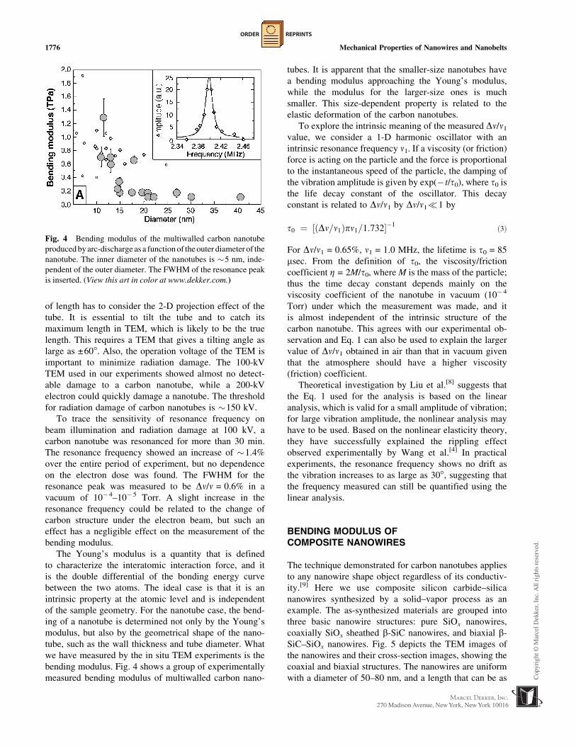
ORDER REPRINTS
of length has to consider the 2-D projection effect of the
tube It is essential to tilt the tube and to catch its
maximum length in TEM which is likely to be the true
length This requires a TEM that gives a tilting angle as
large as plusmn60 Also the operation voltage of the TEM is
important to minimize radiation damage The 100-kV
TEM used in our experiments showed almost no detect-
able damage to a carbon nanotube while a 200-kV
electron could quickly damage a nanotube The threshold
for radiation damage of carbon nanotubes is 150 kV
To trace the sensitivity of resonance frequency on
beam illumination and radiation damage at 100 kV a
carbon nanotube was resonanced for more than 30 min
The resonance frequency showed an increase of 14
over the entire period of experiment but no dependence
on the electron dose was found The FWHM for the
resonance peak was measured to be Dnn = 06 in a
vacuum of 104ndash105 Torr A slight increase in the
resonance frequency could be related to the change of
carbon structure under the electron beam but such an
effect has a negligible effect on the measurement of the
bending modulus
The Youngrsquos modulus is a quantity that is defined
to characterize the interatomic interaction force and it
is the double differential of the bonding energy curve
between the two atoms The ideal case is that it is an
intrinsic property at the atomic level and is independent
of the sample geometry For the nanotube case the bend-
ing of a nanotube is determined not only by the Youngrsquos
modulus but also by the geometrical shape of the nano-
tube such as the wall thickness and tube diameter What
we have measured by the in situ TEM experiments is the
bending modulus Fig 4 shows a group of experimentally
measured bending modulus of multiwalled carbon nano-
tubes It is apparent that the smaller-size nanotubes have
a bending modulus approaching the Youngrsquos modulus
while the modulus for the larger-size ones is much
smaller This size-dependent property is related to the
elastic deformation of the carbon nanotubes
To explore the intrinsic meaning of the measured Dnn1
value we consider a 1-D harmonic oscillator with an
intrinsic resonance frequency n1 If a viscosity (or friction)
force is acting on the particle and the force is proportional
to the instantaneous speed of the particle the damping of
the vibration amplitude is given by exp( tt0) where t0 is
the life decay constant of the oscillator This decay
constant is related to Dnn1 by Dnn11 by
t0 frac14 frac12ethDn=n1THORNpn1=17321 eth3THORN
For Dnn1 = 065 n1 = 10 MHz the lifetime is t0 = 85
msec From the definition of t0 the viscosityfriction
coefficient Z = 2Mt0 where M is the mass of the particle
thus the time decay constant depends mainly on the
viscosity coefficient of the nanotube in vacuum (104
Torr) under which the measurement was made and it
is almost independent of the intrinsic structure of the
carbon nanotube This agrees with our experimental ob-
servation and Eq 1 can also be used to explain the larger
value of Dnn1 obtained in air than that in vacuum given
that the atmosphere should have a higher viscosity
(friction) coefficient
Theoretical investigation by Liu et al[8] suggests that
the Eq 1 used for the analysis is based on the linear
analysis which is valid for a small amplitude of vibration
for large vibration amplitude the nonlinear analysis may
have to be used Based on the nonlinear elasticity theory
they have successfully explained the rippling effect
observed experimentally by Wang et al[4] In practical
experiments the resonance frequency shows no drift as
the vibration increases to as large as 30 suggesting that
the frequency measured can still be quantified using the
linear analysis
BENDING MODULUS OFCOMPOSITE NANOWIRES
The technique demonstrated for carbon nanotubes applies
to any nanowire shape object regardless of its conductiv-
ity[9] Here we use composite silicon carbidendashsilica
nanowires synthesized by a solidndashvapor process as an
example The as-synthesized materials are grouped into
three basic nanowire structures pure SiOx nanowires
coaxially SiOx sheathed b-SiC nanowires and biaxial b-
SiCndashSiOx nanowires Fig 5 depicts the TEM images of
the nanowires and their cross-section images showing the
coaxial and biaxial structures The nanowires are uniform
with a diameter of 50ndash80 nm and a length that can be as
Fig 4 Bending modulus of the multiwalled carbon nanotube
produced by arc-discharge as a function of the outer diameter of the
nanotube The inner diameter of the nanotubes is 5 nm inde-
pendent of the outer diameter The FWHM of the resonance peak
is inserted (View this art in color at wwwdekkercom)
1776 Mechanical Properties of Nanowires and Nanobelts
ORDER REPRINTS
long as 100 mm The coaxial SiCndashSiOx nanowires have
been extensively studied and have a h111i growth
direction with a high density of twins and stacking faults
perpendicular to the growth direction
For a beam with one end hinged and the other free the
resonance frequency is given by[7]
n0 frac14 ethb2=2pTHORNethEI=mTHORN1=2=L2 eth4THORN
where no is the fundamental resonance frequency
b = 1875 EI is the flexural rigidity (or bending stiffness)
E is the Youngrsquos modulus I is the moment of inertia about
a particular axis of the rod L is the length of the beam and
m is its mass per unit length For a uniform solid beam
with a coaxial cable structured nanowire whose core
material density is rc and diameter is Dc and a sheath
material density that is rs with outer diameter Ds the
average density of the nanowire is given by
re frac14 rcethD2c=D2
s THORN thorn rseth1 D2c=D2
s THORN eth5THORN
The effective Youngrsquos modulus of the composite nano-
wire Eeff is
Eeff frac14 refrac128pf0L2=b2Ds2 eth6THORN
The bending modulus for the coaxial cable structured
SiCndashSiOx nanowires results in combination from SiC and
SiOx where the contribution from the sheath layer of SiOx
is more than that from the SiC core because of its larger
flexural rigidity (or bending stiffness) The bending
modulus increases as the diameter of the nanowire
increases (Table 1) consistent with the theoretically
expected values of Eeff = aESiC +(1a)ESilica where
a = (DcDs)4 The data match well to the calculated values
for larger diameter nanowires
From the cross-sectional TEM image of a biaxially
structured nanowire the outermost contour of the cross
section of the nanowire can be approximated to be
elliptical Thus the effective Youngrsquos modulus of the
nanowire can be calculated using Eq 6 with the
introduction of an effective moment of inertia and density
For an elliptical cross section of half long-axis a and
half short-axis b the moments of inertia are Ix = pab34
and Iy = pba34 where a and b can be calculated from
the widths of the composite nanowire With considera-
tion of the equal probability of resonance with respect
to the x and y axes the effective moment of inertia
introduced in the calculation is taken to be approximately
I = (Ix+ Iy)2 and the density per unit length is meff =
Table 1 Measured Youngrsquos modulus of coaxial cable structured SiCndashSiOx nanowires (SiC is the core and silica is the sheath)
(rSilica = 22103 kgm3 rSiC = 32103 kgm3) The Youngrsquos modulii of the bulk materials are ESiC = 466 GPa and ESilica = 73 GPa
Ds (nm)
(plusmn2 nm)
Dc (nm)
(plusmn1 nm)
L (mmm)
(plusmn02 mmm) fo (MHz)
Eeff (GPa)
experimental
Eeff (GPa)
theoretical
51 125 68 0693 46plusmn90 73
74 26 73 0953 56plusmn92 78
83 33 72 1044 52plusmn82 82
132 48 135 0588 78plusmn70 79
190 105 190 0419 81plusmn51 109
Fig 5 (ab) TEM images of the coaxial and biaxial structured
SiCndashSiOx nanowires and (cd) the cross-sectional TEM
images respectively
Mechanical Properties of Nanowires and Nanobelts 1777
M
ORDER REPRINTS
ASiCrSiC+ASilicarSilica where ASiC and ASilica are the cross
sectional areas of the SiC and SiOx sides respectively
The experimentally measured Youngrsquos modulus is given
in Table 2
BENDING MODULUS OF OXIDE NANOBELTS
NanobeltsmdashStructurallyControlled Nanowires
In the literature there are a few names being used for
describing 1-D elongated structures such as nanorod
nanowire nanoribbon nanofiber and nanobelts When we
named the nanostructures to be lsquolsquonanobeltsrsquorsquo[10] we mean
that the nanostructure has specific growth direction the
topbottom surfaces and side surfaces are well-defined
crystallographic facets The requirements for nanowires
are less restrictive than for nanobelts because a wire has a
specific growth direction but its side surfaces may not be
well defined and its cross section may not be uniform nor
have a specific shape Therefore we believe that nano-
belts are more structurally controlled objects than
nanowires or simply a nanobelt is a nanowire that has
well-defined side surfaces It is well known that the
physical property of a carbon nanotube is determined by
the helical angle at which the graphite layer was rolled up
It is expected that for thin nanobelts and nanowires their
physical and chemical properties will depend on the
nature of the side surfaces
The most typical nanobelt is ZnO (Fig 6a) which has a
distinct cross section from the nanotubes or nanowires[10]
Each nanobelt has a uniform width along its entire length
and the typical widths of the nanobelts are in the range
of 50 to 300 nm A ripple-like contrast appearing in the
TEM image is due to the strain resulting from the bending
of the belt High-resolution TEM (HRTEM) and electron
diffraction studies show that the ZnO nanobelts are
structurally uniform single crystalline and dislocation
free (Fig 6b)
There are a few kinds of nanobelts that have been
reported in the literature Table 3 summarizes the nanobelt
structures of function oxides[10ndash14] Each type of nano-
belts is defined by its crystallographic structure the
growth direction top surfaces and side surfaces Some
of the materials can grow along two directions but they
can be controlled experimentally Although these mate-
rials belong to different crystallographic families they
do have a common faceted structure which is the nano-
belt structure In addition nanobelts of Cu(OH)2[15]
MoO3[1617] MgO[1819] and CuO[20]
Table 2 Measured Youngrsquos modulus of biaxially structured SiCndashSiOx nanowires Dwire and DSiC are
the widths across the entire nanowire and across the SiC subnanowire respectively
Dwire (nm)
(plusmn2 nm)
DSiC (nm)
(plusmn1 nm)
L (Mm)
(plusmn02 Mm) fo (MHz)
Eeff (GPa)
experimental
58 24 43 1833 54plusmn241
70 36 79 0629 53plusmn84
83 41 43 2707 61plusmn138
92 47 57 1750 64plusmn143
Fig 6 (a) TEM image of ZnO nanobelts synthesized by a solidndashvapor phase technique (b) High-resolution TEM image of a ZnO
nanobelt with incident electron beam direction along frac122110 The nanobelt grows along [0001] with topbottom surfaces eth2110THORN and side
surfaces eth0110THORN
1778 Mechanical Properties of Nanowires and Nanobelts
ORDER REPRINTS
Dual-Mode Resonance of Nanobelts
Because of the mirror symmetry and rectangular cross
section of the nanobelt (Fig 7a) there are two distinct
fundamental resonance frequencies corresponding to the
vibration in the thickness and width directions which are
given from the classical elasticity theory as[21]
nx frac14 b21T
4pL2
ffiffiffiffiffiffiEx
3r
seth7THORN
ny frac14 b21W
4pL2
ffiffiffiffiffiffiEy
3r
seth8THORN
where b1 = 1875 Ex and Ey are the bending modulus
if the vibration is along the x axis (thickness direction)
and y direction (width direction) respectively r is the
density L is the length W is the width and T is the
thickness of the nanobelt The two modes are decoupled
and they can be observed separately in experiments
Changing the frequency of the applied voltage we
found two fundamental frequencies in two orthogonal
directions transverse to the nanobelt[21] Fig 7c and d
shows the harmonic resonance with the vibration planes
nearly perpendicular and parallel to the viewing direction
respectively For calculating the bending modulus it is
critical to accurately measure the fundamental resonance
frequency (n1) and the dimensional sizes (L and T and W )
of the investigated ZnO nanobelts To determine n1 we
have checked the stability of the resonance frequency to
ensure that one end of the nanobelt is tightly fixed and the
resonant excitation has been carefully checked around the
half value of the resonance frequency
Fig 7 A selected ZnO nanobelt at (ab) stationary (c) the first harmonic resonance in the x direction nx1 =622 kHz and (d) the first
harmonic resonance in the y direction ny1 =691 kHz (e) An enlarged image of the nanobelt and its electron diffraction pattern (inset)
The projected shape of the nanobelt is apparent (f) The FWHM of the resonance peak measured from another ZnO nanobelt The
resonance occurs at 2309 kHz
Table 3 Crystallographic geometry of functional oxide nanobelts
Nanobelt Crystal structure Growth direction Top surface Side surface
ZnO Wurtzite [0001] or frac120110 plusmneth2110THORN or plusmneth2110THORN plusmneth0110THORN or plusmn(0001)
Ga2O3 Monoclinic [001] or [010] plusmn(100) or plusmn(100) plusmn(010) or plusmneth101THORNt-SnO2 Rutile [101] plusmneth101THORN plusmn(010)
o-SnO2 wire Orthorhombic [010] plusmn(100) plusmn(001)
In2O3 C-Rare earth [001] plusmn(100) plusmn(010)
CdO NaCl [001] plusmn(100) plusmn(010)
PbO2 Rutile [010] plusmn(201) plusmneth101THORN
Mechanical Properties of Nanowires and Nanobelts 1779
M
ORDER REPRINTS
ZnO nanobelts can be used as a force sensor Fig 8a
shows a selected ZnO nanobelt with a hooked end which
is equivalent to a cantilever with an integrated tip Be-
cause of the two transverse vibration modes of the
nanobelt resonance along two orthogonal directions has
been observed (Fig 8b and c) The two resonance modes
just correspond to the two modes of the tip operation
when the nanobelt-base cantilever is used as a force
sensor one is the tapping mode and the other is the
noncontact mode Thus the force sensor fabricated using
the ZnO nanobelts is versatile for applications on hard and
soft surfaces
Bending Modulus of Nanobelt
The geometrical parameters are the key for derivation of
the mechanical property from the measured resonance
frequencies The specimen holder is rotated about its axis
so that the nanobelt is aligned perpendicular to the
electron beam thus the real length (L) of the nanobelt can
be obtained The normal direction of the wide facet of the
nanobelt could be firstly determined by electron diffrac-
tion pattern which was frac122110 for the ZnO nanobelt Then
the nanobelt was tilted from its normal direction by
rotating the specimen holder and the tilting direction and
angle were determined by the corresponding electron
diffraction pattern As shown in the inset of Fig 7e the
electron beam direction is frac121100 The angle between
frac121100 and frac122110 is 30 ie the normal direction of the
wide facet of this nanobelt is 30 tilted from the direction
of the electron beam Using the projected dimension
measured from the TEM image (Fig 7e) the geometrical
parameters of this nanobelt are determined to be W = 28
nm and T = 19 nm Based on the experimentally measured
data the bending modulus of the ZnO nanobelts is
calculated using Eqs 7 and 8 The experimental results are
summarized in Table 4[21] The bending modulus of the
ZnO nanobelts was 52 GPa This value represents the
modulus that includes the scaling effect and geometrical
shape and it cannot be directly compared to the Youngrsquos
modulus of ZnO (c33 = 210 GPa c13 = 104 GPa)[22]
because the shape of the nanobelt and the anisotropic
structure of ZnO are convoluted in the measurement The
bending modulus measured by the resonance technique
however has excellent agreement with the elastic modu-
lus measured by nanoindentation for the same type of
nanobelts[23]
Although nanobelts of different sizes may have a slight
difference in bending modulus there is no obvious
difference if the calculation was done using either Eq 7
or Eq 8 The ratio of two fundamental frequencies ny1
nx1 is consistent with the aspect ratio WT as expected
from Eqs 7 and 8 because there is no significant dif-
ference between Ex and Ey
The resonance technique demonstrated here is very
sensitive to the structure of a nanowire Fig 9a and b
shows a silicon nanowire that has a Au tip but the Au
Fig 8 A selected ZnO nanobelt with a hooked end at (a)
stationary (b) resonance at 731 kHz in the plane almost parallel
to the viewing direction and (c) resonance at 474 kHz in the
place closely perpendicular to the viewing direction
Table 4 Bending modulus of the ZnO nanobelts Ex and Ey represents the bending modulus corresponding to the resonance along the
thickness and width directions respectively
Nanobelt
Length
L (mmm)
(plusmn005)
Width
W (nm) (plusmn1)
Thickness
T (nm) (plusmn1)
Fundamental frequency (kHz)
Bending modulus
(GPa)
WT nnx1 nny1 nny1nnx1 Ex Ey
1 825 55 33 17 232 373 16 466plusmn06 501plusmn06
2 473 28 19 15 396 576 14 443plusmn13 455plusmn29
3 407 31 20 16 662 958 14 563plusmn09 646plusmn23
4 890 44 39 11 210 231 11 379plusmn06 399plusmn12
1780 Mechanical Properties of Nanowires and Nanobelts
ORDER REPRINTS
particle is off the symmetric axis of the nanowire This
asymmetric structure results in two distinct resonance
along two perpendicular directions (Fig 9c and d) The
difference between the two resonance frequencies is re-
lated to the mass of the Au particle
THE HARDNESS OF A NANOBELTBY NANOINDENTATION
Nanoscale mechanical properties of individual zinc oxide
nanobelts were characterized by Nanoscope IIIa atomic
Fig 9 (a) A silicon nanowire with a gold particle at the tip showing (bc) two independent resonance along two perpen-
dicular directions
Fig 10 (a) Schematic of nanoindentation on ZnO by AFM tip (bc) AFM image of a nanobelt before and after being indented
showing plastic deformation on the surfaces (d) Hardness of ZnO and SnO2 nanobelts as a function of penetration during
nanoindentation (View this art in color at wwwdekkercom)
Mechanical Properties of Nanowires and Nanobelts 1781
M
ORDER REPRINTS
force microscope (AFM) (Fig 10a) and Hysitron Tribo-
Scope with homemade side-view CCD camera[23] The
prepared nanobelt sample was investigated by two means
one is by tapping mode of Nanoscope IIIa using a
diamond indenter tip with a radius of lt25 nm The other is
by STM mode of Hysitron TriboScope an add-on force
transducer from Hysitron Inc using a diamond cubic
corner tip with a radius of lt40 nm In either case in-
dividual nanobelts were imaged and then nanoindenta-
tions were made on the nanobelt using varied loads
(Fig 10b and c) After indentation the indent was imaged
in situ using the image mode of the AFM For nanoin-
dentations the hardness is normally defined as the maxi-
mum load divided by the projected area of the indenter in
contact with the sample at the maximum load Thus
H frac14 PMAX
AC
eth9THORN
where H PMAX and AC are the hardness maximum
applied load and projected contact area at the maximum
applied load respectively Because the indenter tip is not
rigid during indentation the elastic modulus cannot be
directly determined from the load vs the displacement
curve However the reduced elastic modulus can be
determined from the unloading portion of the curve by
the relation
Er frac14ffiffiffip
p
2 dP
dh 1ffiffiffiffiffi
Ac
p eth10THORN
where Er and dPdh are the reduced modulus and
experimentally measured stiffness respectively
Based on Eq 9 using load vs deflection curves
during nanoindentation the hardness of ZnO and SnO2
nanobelts was calculated as a function of indentation
penetration and the result is summarized in Fig 10d
The hardness of ZnO is lower than that in the SnO2
nanobelt Also it can be seen that the lower the
penetration of the nanoindentation the higher the
hardness of the nanobelt which is attributed to the strain
gradient effect (size effect) during nanoindentation for
most materials[24] The effective elastic modulus can also
be derived from the forcendashdisplacement curve and the
result is E = 45 GPa for ZnO in good agreement with
that from the resonance technique[21]
NANOBELTS AS NANOCANTILEVERS
The cantilever-based scanning probe microscopy (SPM)
technique is one of the most powerful approaches in
imaging manipulating and measuring nanoscale proper-
ties and phenomena The most conventional cantilever
used for SPM is based on silicon Si3N4 or SiC which is
fabricated by e-beam or optical lithography technique and
typically has a dimension of thickness of 100 nm width
of 5 mm and length of 50 mm Utilization of nano-
wire- and nanotube-based cantilevers can have several
advantages for SPM Carbon nanotubes can be grown
on the tip of a conventional cantilever and be used for
imaging surfaces with a large degree of abrupt variation in
surface morphology[2526] We demonstrate here the
manipulation of nanobelts by AFM and its potential as
nanocantilevers[27]
Manipulation of nanobelts is important for integrating
this structurally controlled nanomaterial with microelec-
trical mechanical system (MEMS) Using an AFM tip
a nanobelt can be manipulated into different shapes
(Fig 11) A ZnO nanobelt of 56 nm in width can be bent
for over 60 without breaking demonstrating extremely
high mechanical flexibility Further bending bent the
nanobelt into two segments This is a technique for cutting
a nanobelt into specific length
Combining MEMS technology with self-assembled
nanobelts we are able to produce cost-effective canti-
levers with much heightened sensitivity for a range of
Fig 11 A series of shape of a ZnO nanobelt created by
manipulation using an AFM tip showing deformation and
break-up (Image courtesy of MS Arnold Ph Avouris) (View
this art in color at wwwdekkercom)
1782 Mechanical Properties of Nanowires and Nanobelts
ORDER REPRINTS
devices and applications Force pressure mass thermal
biological and chemical sensors are all prospective
devices Semiconducting nanobelts are ideal candidates
for cantilever applications Structurally they are defect-
free single crystals providing excellent mechanical
properties The reduced dimensions of nanobelt cantile-
vers offer a significant increase in cantilever sensitivity
The cantilevers under consideration are simple in design
and practice Using a Dimension 3000 SPM in tapping
mode we have successfully lifted ZnO nanobelts from a
silicon substrate Capillary forces are responsible for the
adhesion strength between the AFM probe and the ZnO
nanobelts Combining the aforementioned techniques
with micromanipulation has led to the alignment of
individual ZnO nanobelts onto silicon chips (Fig 12)
The aligned ZnO cantilevers were manipulated to have a
range of lengths This exemplifies our ability to tune the
resonance frequency of each cantilever and thus modify
cantilevers for different applications such as tapping and
contact mode AFM The nanobelt-based nanocantilever
is 50ndash1000 times smaller than the conventional
cantilever Decreased size in microoptical mechanical
devices corresponds to increased sensitivity Combining
the aforementioned techniques with micromanipulation
has led to the horizontal alignment of individual ZnO
nanobelts onto silicon chips (Fig 12) This exempli-
fies our ability to tune the resonance frequency of each
cantilever and thus modify cantilevers for different
applications such as contact noncontact and tapping
mode AFM
THE WORK FUNCTION AT THE TIP OF ANANOBELT BY RESONANCE TECHNIQUE
The field-emission property for well-aligned ZnO nano-
wire arrays has been reported[28] demonstrating a promis-
ing application of semiconductor nanowires as field
emitters for flat panel display Following the Fowlerndash
Nordheim (FndashN) theory[29] an important physical quantity
in electron field emission is the surface work function
which is well documented for elemental materials For
the emitters such as ZnO nanowire arrays most of the
electrons are emitted from tips of the nanowires and it is
the local work function that matters to the properties of the
field emission However the work function measured
based on the FndashN theory is an average over the large scale
of emitting materials So it is necessary to measure the
local work function at the tip of an individual emitter Gao
et al[30] have measured the work function at the tips of
carbon nanotubes by an in situ TEM technique The
measurement relies on the mechanical resonance of the
carbon nanotube induced by an externally applied oscil-
lating voltage with tunable frequency
The measurement of the work function at the tip of a
single ZnO nanobelt was carried out in situ at 200 kV in a
Hitachi HF-2000 FEG TEM A specimen holder was built
for applying a voltage across a nanobelt and its counter
gold electrode The nanobelts to be used for measurements
are directly imaged under TEM Fig 13 is a setup for work
function measurement One end of the nanobelt was
electrically attached to a gold wire and the other end
Fig 12 Site-specific placement and alignment of ZnO nanobelts onto a silicon chip forming nanocantilever arrays The inset is an
enlarged SEM image of the third nanocantilever showing its shape the width of the cantilever was measured to be 525 nm
Mechanical Properties of Nanowires and Nanobelts 1783
M
ORDER REPRINTS
faces directly against the gold ball Because of the
difference in the surface work function between the ZnO
nanobelt and the counter Au ball a static charge Q0 exists
at the tip of the nanobelt to balance this potential
difference[31] The magnitude of Q0 is proportional to
the difference between the work function of the nanobelt
tip (NBT) and the Au electrode Q0 = a (fAufNBT)
where a is related to the geometry and distance between
the nanobelt and the electrode
The measurement is based on the mechanical reso-
nance of the nanobelt induced by an externally alternative
electric field Experimentally a constant voltage Vdc and
an oscillating voltage Vaccos2pft are applied onto the
nanobelt (Fig 13a) where f is the frequency and Vac is
the amplitude Thus the total induced charge on the
nanobelt is
Q frac14 Q0 thorn aeethVdc thorn Vac cos 2pftTHORN eth11THORN
The force acting on the nanobelt is proportional to the
square of the total charge on the nanobelt
F frac14 bfrac12Q0 thorn aeethVdc thorn Vac cos 2pftTHORN2
frac14 a2bffrac12ethfAu fNBT thorn eVdcTHORN2 thorn e2V2ac=2
thorn 2eVacethfAu fNBT thorn eVdcTHORN
cos 2pft thorn e2V2ac=2 cos 4pftg
eth12THORN
where b is a proportional constant In Eq 12 the first term
is constant and it causes a static deflection of the ZnO
nanobelt The second term is a linear term and the res-
onance occurs if the applied frequency f is tuned to the
intrinsic mechanical resonance frequency f0 of the ZnO
nanobelt The most important result of Eq 12 is that for
the linear term the resonance amplitude A of the nanobelt
is proportional to Vac(fAufNBT+eVdc)
The principle of the measurement is as follows We
first set Vdc = 0 and tune the frequency f to get the
mechanical resonance induced by the applied oscillat-
ing field Second under the resonance condition of
keeping f = f0 and Vac constant slowly change the mag-
nitude of Vdc from zero to a value Vdc0 that satisfies
fAufNBT+eVdc0 = 0 At this moment the resonance
amplitude A becomes zero although the external ac
voltage is still in effect Therefore the work function at the
tip of the ZnO nanobelt is fNBT = fAu+eVdc0 while
fAu = 51 eV Fig 14 is a plot of the vibration amplitude
A of the nanobelt as a function of the applied direct cur-
rent voltage Vdc from which the value for Vdc0 is
determined The work function of the ZnO nanobelts is
52 eV[32]
CONCLUSION
The property characterization of nanomaterials is chal-
lenged by their small-size structures because of the
difficulties in manipulation A typical example is the me-
chanical properties of individual 1-D nanostructures such
as nanotubes nanowires and nanobelts This chapter
reviews the experimental methods for measuring the
mechanical properties of 1-D nanostructures using a reso-
nance technique in TEM The static and dynamic pro-
perties of the 1-D nanostructures can be obtained by
applying controllable static and alternating electric fields
Fig 14 A plot of vibration amplitude of a ZnO nanobelt as a
function of the applied direct current voltage from which the
offset voltage Vdc0 =012 V
Fig 13 Experimental set-up for measuring the work function
at the tip of a ZnO nanobelt
1784 Mechanical Properties of Nanowires and Nanobelts
ORDER REPRINTS
The resonance of carbon nanotubes can be induced by
tuning the frequency of the applied voltage The technique
is powerful in such a way that it can directly correlate
the atomic-scale microstructure of the carbon nanotube
with its physical properties providing a one-to-one
correspondence in structurendashproperty characterization
Because of the rectangular cross section of the
nanobelt two fundamental resonance modes have been
observed corresponding to two orthogonal transverse
vibration directions showing the versatile applications
of nanobelts as nanocantilevers and nanoresonators The
bending modulus of the ZnO nanobelts was measured to
be 52 GPa Nanobelts have also been demonstrated as
ultrasmall nanocantilevers for sensor and possibly imag-
ing applications in AFM
ACKNOWLEDGMENTS
The results reviewed in this paper were partially contrib-
uted from my group members and collaborators Ruiping
Gao Xuedong Bai Scott Mao William Hughes and Enge
Wang to whom I am very grateful Research supported by
NSF NASA and NSFC
REFERENCES
1 Wang ZL Liu Y Zhang Z Handbook of
Nanophase and Nanostructured Materials 2002
Vols IndashIV Tsinghua University Press Beijing
Kluwer Academic Publisher New York
2 Wang ZL Hui C Electron Microscopy of
Nanotubes Kluwer Academic Publisher New York
2003
3 Poncharal P Wang ZL Ugarte D de Heer
WA Electrostatic deflections and electromechani-
cal resonances of carbon nanotubes Science 1999283 1513ndash1516
4 Wang ZL Poncharal P de Heer WA Nano-
measurements of individual carbon nanotubes by
in-situ TEM Pure Appl Chem 2000 72 209ndash
219
5 Gao RP Wang ZL Bai ZG de Heer WA
Dai LM Gao M Nanomechanics of aligned
carbon nanotube arrays Phys Rev Lett 2000 85622ndash635
6 Wang ZL Poncharal P de Heer WA Measur-
ing physical and mechanical properties of individual
carbon nanotubes by in-situ TEM J Phys Chem
Solids 2000 61 1025ndash1030
7 Meirovich L Elements of Vibration Analysis
McGraw-Hill New York 1986
8 Liu JZ Zheng QS Jiang Q Effect of ripping
mode on resonances of carbon nanotubes Phys Rev
Lett 2001 86 4843ndash4846
9 Wang ZL Dai ZR Bai ZG Gao RP Gole
JL Side-by-side silicon carbide-silica biaxial nano-
wires Synthesis structure and mechanical proper-
ties Appl Phys Lett 2000 77 3349ndash3351
10 Pan ZW Dai ZR Wang ZL Nanobelts of
semiconducting oxides Science 2001 291 1947ndash
1949
11 Wang ZL Pan ZW Dai ZR Semiconducting
Oxide Nanostructures US Patent No 6586095
July 1 2003
12 Dai ZR Pan ZW Wang ZL Gallium oxide
nanoribbons and nanosheets J Phys Chem B
2002 106 902ndash904
13 Dai ZR Pan ZW Wang ZL Growth and
structure evolution of novel tin oxide diskettes J
Am Chem Soc 2002 124 8673ndash8680
14 Kong XY Wang ZL Spontaneous polarization
and helical nanosprings of piezoelectric nanobelts
Nano Lett 2003 in press15 Wen XG Zhang WX Yang SH Dai ZR
Wang ZL Solution phase synthesis of Cu(OH)sub
2nanoribbons by coordination self-assembly using
Cusub 2S nanowires as precursors Nano Lett
2002 2 (12) 1397ndash1401
16 Li YB Bando Y Golberg D Kurashima K
Field emission from MoOsub 3nanobelts Appl
Phys Lett 2002 81 (26) 5048ndash5050
17 Zhou J Xu NS Deng SZ Chen J She JC
Wang ZL Large-area nanowire arrays of molyb-
denum and molybdenum oxides Synthesis and field
emission properties Adv Mater 2003 in press18 Li YB Bando Y Sato T Preparation of
network-like MgO nanobelts on Si substrate Chem
Phys Lett 2002 359 (1ndash2) 141ndash145
19 Liu J Cai J Son YC Gao QM Suib SL
Aindow M Magnesium manganese oxide nano-
ribbons Synthesis characterization and catalytic
application J Phys Chem B 2002 106 (38) 9761
20 Wen XG Zhang WX Yang SH Synthesis of
Cu- (OH)2 and CuO nanoribbon arrays on a copper
surface Langmuir 2003 19 5898ndash5903
21 Bai XD Wang EG Gao PX Wang ZL
Dual-mode mechanical resonance of individual
ZnO nanobelts Appl Phys Lett 2003 824806ndash4808
22 Carlotti G Socino G Petri A Verona E
Acoustic investigation of the elastic properties of
ZnO films Appl Phys Lett 1987 51 1889ndash1891
Mechanical Properties of Nanowires and Nanobelts 1785
M
ORDER REPRINTS
23 Mao SX Zhao MH Wang ZL Probing nano-
scale mechanical properties of individual semicon-
ducting nanobelt Appl Phys Lett 2002 83 993ndash
995
24 Duan DM Wu N Slaughter WS Mao SX
Length scale effect on mechanical behavior due to
strain gradient plasticity Mater Sci Eng A 2001A303 (1ndash2) 241ndash249
25 Yenilmez E Wang Q Chen RJ Wang D
Dai HJ Wafer scale production of carbon
nanotube scanning probe tips for atomic force
microscopy Appl Phys Lett 2002 80 (12)2225ndash2227
26 Dai HJ Hafner JH Rinzler AG Colbert
DT Smalley RE Nanotubes as nanoprobes in
scanning probe microscopy Nature 1996 384147ndash150
27 Hughes W Wang ZL Nanobelt as nanocantile-
ver Appl Phys Lett 2003 82 2886ndash2888
28 Lee CJ Lee TJ Lyu SC Zhang Y Ruh H
Lee HJ Field emission from well-aligned zinc
oxide nanowires grown at low temperature Appl
Phys Lett 2002 81 (19) 3648ndash3650
29 Fowler RH Nordherim LW Electron emission
in intense electric fields Proc R Soc Lond A
1928 119 (781) 173
30 Gao RP Pan ZW Wang ZL Work function at
the tips of multi-walled carbon nanotubes Appl
Phys Lett 2001 78 1757ndash1759
31 Kelvin L Philos Mag 1898 46 82
32 Bai XD Wang EG Gao PX Wang ZL
Measuring the work function at a nanobelt tip and at
a nanoparticle surface Nano Lett 2003 3 1147ndash
1150
1786 Mechanical Properties of Nanowires and Nanobelts
Request PermissionOrder Reprints
Reprints of this article can also be ordered at
httpwwwdekkercomservletproductDOI101081EENN120013387
Request Permission or Order Reprints Instantly
Interested in copying and sharing this article In most cases US Copyright Law requires that you get permission from the articlersquos rightsholder before using copyrighted content
All information and materials found in this article including but not limited to text trademarks patents logos graphics and images (the Materials) are the copyrighted works and other forms of intellectual property of Marcel Dekker Inc or its licensors All rights not expressly granted are reserved
Get permission to lawfully reproduce and distribute the Materials or order reprints quickly and painlessly Simply click on the Request Permission Order Reprints link below and follow the instructions Visit the US Copyright Office for information on Fair Use limitations of US copyright law Please refer to The Association of American Publishersrsquo (AAP) website for guidelines on Fair Use in the Classroom
The Materials are for your personal use only and cannot be reformatted reposted resold or distributed by electronic means or otherwise without permission from Marcel Dekker Inc Marcel Dekker Inc grants you the limited right to display the Materials only on your personal computer or personal wireless device and to copy and download single copies of such Materials provided that any copyright trademark or other notice appearing on such Materials is also retained by displayed copied or downloaded as part of the Materials and is not removed or obscured and provided you do not edit modify alter or enhance the Materials Please refer to our Website User Agreement for more details
ORDER REPRINTS
ASiCrSiC+ASilicarSilica where ASiC and ASilica are the cross
sectional areas of the SiC and SiOx sides respectively
The experimentally measured Youngrsquos modulus is given
in Table 2
BENDING MODULUS OF OXIDE NANOBELTS
NanobeltsmdashStructurallyControlled Nanowires
In the literature there are a few names being used for
describing 1-D elongated structures such as nanorod
nanowire nanoribbon nanofiber and nanobelts When we
named the nanostructures to be lsquolsquonanobeltsrsquorsquo[10] we mean
that the nanostructure has specific growth direction the
topbottom surfaces and side surfaces are well-defined
crystallographic facets The requirements for nanowires
are less restrictive than for nanobelts because a wire has a
specific growth direction but its side surfaces may not be
well defined and its cross section may not be uniform nor
have a specific shape Therefore we believe that nano-
belts are more structurally controlled objects than
nanowires or simply a nanobelt is a nanowire that has
well-defined side surfaces It is well known that the
physical property of a carbon nanotube is determined by
the helical angle at which the graphite layer was rolled up
It is expected that for thin nanobelts and nanowires their
physical and chemical properties will depend on the
nature of the side surfaces
The most typical nanobelt is ZnO (Fig 6a) which has a
distinct cross section from the nanotubes or nanowires[10]
Each nanobelt has a uniform width along its entire length
and the typical widths of the nanobelts are in the range
of 50 to 300 nm A ripple-like contrast appearing in the
TEM image is due to the strain resulting from the bending
of the belt High-resolution TEM (HRTEM) and electron
diffraction studies show that the ZnO nanobelts are
structurally uniform single crystalline and dislocation
free (Fig 6b)
There are a few kinds of nanobelts that have been
reported in the literature Table 3 summarizes the nanobelt
structures of function oxides[10ndash14] Each type of nano-
belts is defined by its crystallographic structure the
growth direction top surfaces and side surfaces Some
of the materials can grow along two directions but they
can be controlled experimentally Although these mate-
rials belong to different crystallographic families they
do have a common faceted structure which is the nano-
belt structure In addition nanobelts of Cu(OH)2[15]
MoO3[1617] MgO[1819] and CuO[20]
Table 2 Measured Youngrsquos modulus of biaxially structured SiCndashSiOx nanowires Dwire and DSiC are
the widths across the entire nanowire and across the SiC subnanowire respectively
Dwire (nm)
(plusmn2 nm)
DSiC (nm)
(plusmn1 nm)
L (Mm)
(plusmn02 Mm) fo (MHz)
Eeff (GPa)
experimental
58 24 43 1833 54plusmn241
70 36 79 0629 53plusmn84
83 41 43 2707 61plusmn138
92 47 57 1750 64plusmn143
Fig 6 (a) TEM image of ZnO nanobelts synthesized by a solidndashvapor phase technique (b) High-resolution TEM image of a ZnO
nanobelt with incident electron beam direction along frac122110 The nanobelt grows along [0001] with topbottom surfaces eth2110THORN and side
surfaces eth0110THORN
1778 Mechanical Properties of Nanowires and Nanobelts
ORDER REPRINTS
Dual-Mode Resonance of Nanobelts
Because of the mirror symmetry and rectangular cross
section of the nanobelt (Fig 7a) there are two distinct
fundamental resonance frequencies corresponding to the
vibration in the thickness and width directions which are
given from the classical elasticity theory as[21]
nx frac14 b21T
4pL2
ffiffiffiffiffiffiEx
3r
seth7THORN
ny frac14 b21W
4pL2
ffiffiffiffiffiffiEy
3r
seth8THORN
where b1 = 1875 Ex and Ey are the bending modulus
if the vibration is along the x axis (thickness direction)
and y direction (width direction) respectively r is the
density L is the length W is the width and T is the
thickness of the nanobelt The two modes are decoupled
and they can be observed separately in experiments
Changing the frequency of the applied voltage we
found two fundamental frequencies in two orthogonal
directions transverse to the nanobelt[21] Fig 7c and d
shows the harmonic resonance with the vibration planes
nearly perpendicular and parallel to the viewing direction
respectively For calculating the bending modulus it is
critical to accurately measure the fundamental resonance
frequency (n1) and the dimensional sizes (L and T and W )
of the investigated ZnO nanobelts To determine n1 we
have checked the stability of the resonance frequency to
ensure that one end of the nanobelt is tightly fixed and the
resonant excitation has been carefully checked around the
half value of the resonance frequency
Fig 7 A selected ZnO nanobelt at (ab) stationary (c) the first harmonic resonance in the x direction nx1 =622 kHz and (d) the first
harmonic resonance in the y direction ny1 =691 kHz (e) An enlarged image of the nanobelt and its electron diffraction pattern (inset)
The projected shape of the nanobelt is apparent (f) The FWHM of the resonance peak measured from another ZnO nanobelt The
resonance occurs at 2309 kHz
Table 3 Crystallographic geometry of functional oxide nanobelts
Nanobelt Crystal structure Growth direction Top surface Side surface
ZnO Wurtzite [0001] or frac120110 plusmneth2110THORN or plusmneth2110THORN plusmneth0110THORN or plusmn(0001)
Ga2O3 Monoclinic [001] or [010] plusmn(100) or plusmn(100) plusmn(010) or plusmneth101THORNt-SnO2 Rutile [101] plusmneth101THORN plusmn(010)
o-SnO2 wire Orthorhombic [010] plusmn(100) plusmn(001)
In2O3 C-Rare earth [001] plusmn(100) plusmn(010)
CdO NaCl [001] plusmn(100) plusmn(010)
PbO2 Rutile [010] plusmn(201) plusmneth101THORN
Mechanical Properties of Nanowires and Nanobelts 1779
M
ORDER REPRINTS
ZnO nanobelts can be used as a force sensor Fig 8a
shows a selected ZnO nanobelt with a hooked end which
is equivalent to a cantilever with an integrated tip Be-
cause of the two transverse vibration modes of the
nanobelt resonance along two orthogonal directions has
been observed (Fig 8b and c) The two resonance modes
just correspond to the two modes of the tip operation
when the nanobelt-base cantilever is used as a force
sensor one is the tapping mode and the other is the
noncontact mode Thus the force sensor fabricated using
the ZnO nanobelts is versatile for applications on hard and
soft surfaces
Bending Modulus of Nanobelt
The geometrical parameters are the key for derivation of
the mechanical property from the measured resonance
frequencies The specimen holder is rotated about its axis
so that the nanobelt is aligned perpendicular to the
electron beam thus the real length (L) of the nanobelt can
be obtained The normal direction of the wide facet of the
nanobelt could be firstly determined by electron diffrac-
tion pattern which was frac122110 for the ZnO nanobelt Then
the nanobelt was tilted from its normal direction by
rotating the specimen holder and the tilting direction and
angle were determined by the corresponding electron
diffraction pattern As shown in the inset of Fig 7e the
electron beam direction is frac121100 The angle between
frac121100 and frac122110 is 30 ie the normal direction of the
wide facet of this nanobelt is 30 tilted from the direction
of the electron beam Using the projected dimension
measured from the TEM image (Fig 7e) the geometrical
parameters of this nanobelt are determined to be W = 28
nm and T = 19 nm Based on the experimentally measured
data the bending modulus of the ZnO nanobelts is
calculated using Eqs 7 and 8 The experimental results are
summarized in Table 4[21] The bending modulus of the
ZnO nanobelts was 52 GPa This value represents the
modulus that includes the scaling effect and geometrical
shape and it cannot be directly compared to the Youngrsquos
modulus of ZnO (c33 = 210 GPa c13 = 104 GPa)[22]
because the shape of the nanobelt and the anisotropic
structure of ZnO are convoluted in the measurement The
bending modulus measured by the resonance technique
however has excellent agreement with the elastic modu-
lus measured by nanoindentation for the same type of
nanobelts[23]
Although nanobelts of different sizes may have a slight
difference in bending modulus there is no obvious
difference if the calculation was done using either Eq 7
or Eq 8 The ratio of two fundamental frequencies ny1
nx1 is consistent with the aspect ratio WT as expected
from Eqs 7 and 8 because there is no significant dif-
ference between Ex and Ey
The resonance technique demonstrated here is very
sensitive to the structure of a nanowire Fig 9a and b
shows a silicon nanowire that has a Au tip but the Au
Fig 8 A selected ZnO nanobelt with a hooked end at (a)
stationary (b) resonance at 731 kHz in the plane almost parallel
to the viewing direction and (c) resonance at 474 kHz in the
place closely perpendicular to the viewing direction
Table 4 Bending modulus of the ZnO nanobelts Ex and Ey represents the bending modulus corresponding to the resonance along the
thickness and width directions respectively
Nanobelt
Length
L (mmm)
(plusmn005)
Width
W (nm) (plusmn1)
Thickness
T (nm) (plusmn1)
Fundamental frequency (kHz)
Bending modulus
(GPa)
WT nnx1 nny1 nny1nnx1 Ex Ey
1 825 55 33 17 232 373 16 466plusmn06 501plusmn06
2 473 28 19 15 396 576 14 443plusmn13 455plusmn29
3 407 31 20 16 662 958 14 563plusmn09 646plusmn23
4 890 44 39 11 210 231 11 379plusmn06 399plusmn12
1780 Mechanical Properties of Nanowires and Nanobelts
ORDER REPRINTS
particle is off the symmetric axis of the nanowire This
asymmetric structure results in two distinct resonance
along two perpendicular directions (Fig 9c and d) The
difference between the two resonance frequencies is re-
lated to the mass of the Au particle
THE HARDNESS OF A NANOBELTBY NANOINDENTATION
Nanoscale mechanical properties of individual zinc oxide
nanobelts were characterized by Nanoscope IIIa atomic
Fig 9 (a) A silicon nanowire with a gold particle at the tip showing (bc) two independent resonance along two perpen-
dicular directions
Fig 10 (a) Schematic of nanoindentation on ZnO by AFM tip (bc) AFM image of a nanobelt before and after being indented
showing plastic deformation on the surfaces (d) Hardness of ZnO and SnO2 nanobelts as a function of penetration during
nanoindentation (View this art in color at wwwdekkercom)
Mechanical Properties of Nanowires and Nanobelts 1781
M
ORDER REPRINTS
force microscope (AFM) (Fig 10a) and Hysitron Tribo-
Scope with homemade side-view CCD camera[23] The
prepared nanobelt sample was investigated by two means
one is by tapping mode of Nanoscope IIIa using a
diamond indenter tip with a radius of lt25 nm The other is
by STM mode of Hysitron TriboScope an add-on force
transducer from Hysitron Inc using a diamond cubic
corner tip with a radius of lt40 nm In either case in-
dividual nanobelts were imaged and then nanoindenta-
tions were made on the nanobelt using varied loads
(Fig 10b and c) After indentation the indent was imaged
in situ using the image mode of the AFM For nanoin-
dentations the hardness is normally defined as the maxi-
mum load divided by the projected area of the indenter in
contact with the sample at the maximum load Thus
H frac14 PMAX
AC
eth9THORN
where H PMAX and AC are the hardness maximum
applied load and projected contact area at the maximum
applied load respectively Because the indenter tip is not
rigid during indentation the elastic modulus cannot be
directly determined from the load vs the displacement
curve However the reduced elastic modulus can be
determined from the unloading portion of the curve by
the relation
Er frac14ffiffiffip
p
2 dP
dh 1ffiffiffiffiffi
Ac
p eth10THORN
where Er and dPdh are the reduced modulus and
experimentally measured stiffness respectively
Based on Eq 9 using load vs deflection curves
during nanoindentation the hardness of ZnO and SnO2
nanobelts was calculated as a function of indentation
penetration and the result is summarized in Fig 10d
The hardness of ZnO is lower than that in the SnO2
nanobelt Also it can be seen that the lower the
penetration of the nanoindentation the higher the
hardness of the nanobelt which is attributed to the strain
gradient effect (size effect) during nanoindentation for
most materials[24] The effective elastic modulus can also
be derived from the forcendashdisplacement curve and the
result is E = 45 GPa for ZnO in good agreement with
that from the resonance technique[21]
NANOBELTS AS NANOCANTILEVERS
The cantilever-based scanning probe microscopy (SPM)
technique is one of the most powerful approaches in
imaging manipulating and measuring nanoscale proper-
ties and phenomena The most conventional cantilever
used for SPM is based on silicon Si3N4 or SiC which is
fabricated by e-beam or optical lithography technique and
typically has a dimension of thickness of 100 nm width
of 5 mm and length of 50 mm Utilization of nano-
wire- and nanotube-based cantilevers can have several
advantages for SPM Carbon nanotubes can be grown
on the tip of a conventional cantilever and be used for
imaging surfaces with a large degree of abrupt variation in
surface morphology[2526] We demonstrate here the
manipulation of nanobelts by AFM and its potential as
nanocantilevers[27]
Manipulation of nanobelts is important for integrating
this structurally controlled nanomaterial with microelec-
trical mechanical system (MEMS) Using an AFM tip
a nanobelt can be manipulated into different shapes
(Fig 11) A ZnO nanobelt of 56 nm in width can be bent
for over 60 without breaking demonstrating extremely
high mechanical flexibility Further bending bent the
nanobelt into two segments This is a technique for cutting
a nanobelt into specific length
Combining MEMS technology with self-assembled
nanobelts we are able to produce cost-effective canti-
levers with much heightened sensitivity for a range of
Fig 11 A series of shape of a ZnO nanobelt created by
manipulation using an AFM tip showing deformation and
break-up (Image courtesy of MS Arnold Ph Avouris) (View
this art in color at wwwdekkercom)
1782 Mechanical Properties of Nanowires and Nanobelts
ORDER REPRINTS
devices and applications Force pressure mass thermal
biological and chemical sensors are all prospective
devices Semiconducting nanobelts are ideal candidates
for cantilever applications Structurally they are defect-
free single crystals providing excellent mechanical
properties The reduced dimensions of nanobelt cantile-
vers offer a significant increase in cantilever sensitivity
The cantilevers under consideration are simple in design
and practice Using a Dimension 3000 SPM in tapping
mode we have successfully lifted ZnO nanobelts from a
silicon substrate Capillary forces are responsible for the
adhesion strength between the AFM probe and the ZnO
nanobelts Combining the aforementioned techniques
with micromanipulation has led to the alignment of
individual ZnO nanobelts onto silicon chips (Fig 12)
The aligned ZnO cantilevers were manipulated to have a
range of lengths This exemplifies our ability to tune the
resonance frequency of each cantilever and thus modify
cantilevers for different applications such as tapping and
contact mode AFM The nanobelt-based nanocantilever
is 50ndash1000 times smaller than the conventional
cantilever Decreased size in microoptical mechanical
devices corresponds to increased sensitivity Combining
the aforementioned techniques with micromanipulation
has led to the horizontal alignment of individual ZnO
nanobelts onto silicon chips (Fig 12) This exempli-
fies our ability to tune the resonance frequency of each
cantilever and thus modify cantilevers for different
applications such as contact noncontact and tapping
mode AFM
THE WORK FUNCTION AT THE TIP OF ANANOBELT BY RESONANCE TECHNIQUE
The field-emission property for well-aligned ZnO nano-
wire arrays has been reported[28] demonstrating a promis-
ing application of semiconductor nanowires as field
emitters for flat panel display Following the Fowlerndash
Nordheim (FndashN) theory[29] an important physical quantity
in electron field emission is the surface work function
which is well documented for elemental materials For
the emitters such as ZnO nanowire arrays most of the
electrons are emitted from tips of the nanowires and it is
the local work function that matters to the properties of the
field emission However the work function measured
based on the FndashN theory is an average over the large scale
of emitting materials So it is necessary to measure the
local work function at the tip of an individual emitter Gao
et al[30] have measured the work function at the tips of
carbon nanotubes by an in situ TEM technique The
measurement relies on the mechanical resonance of the
carbon nanotube induced by an externally applied oscil-
lating voltage with tunable frequency
The measurement of the work function at the tip of a
single ZnO nanobelt was carried out in situ at 200 kV in a
Hitachi HF-2000 FEG TEM A specimen holder was built
for applying a voltage across a nanobelt and its counter
gold electrode The nanobelts to be used for measurements
are directly imaged under TEM Fig 13 is a setup for work
function measurement One end of the nanobelt was
electrically attached to a gold wire and the other end
Fig 12 Site-specific placement and alignment of ZnO nanobelts onto a silicon chip forming nanocantilever arrays The inset is an
enlarged SEM image of the third nanocantilever showing its shape the width of the cantilever was measured to be 525 nm
Mechanical Properties of Nanowires and Nanobelts 1783
M
ORDER REPRINTS
faces directly against the gold ball Because of the
difference in the surface work function between the ZnO
nanobelt and the counter Au ball a static charge Q0 exists
at the tip of the nanobelt to balance this potential
difference[31] The magnitude of Q0 is proportional to
the difference between the work function of the nanobelt
tip (NBT) and the Au electrode Q0 = a (fAufNBT)
where a is related to the geometry and distance between
the nanobelt and the electrode
The measurement is based on the mechanical reso-
nance of the nanobelt induced by an externally alternative
electric field Experimentally a constant voltage Vdc and
an oscillating voltage Vaccos2pft are applied onto the
nanobelt (Fig 13a) where f is the frequency and Vac is
the amplitude Thus the total induced charge on the
nanobelt is
Q frac14 Q0 thorn aeethVdc thorn Vac cos 2pftTHORN eth11THORN
The force acting on the nanobelt is proportional to the
square of the total charge on the nanobelt
F frac14 bfrac12Q0 thorn aeethVdc thorn Vac cos 2pftTHORN2
frac14 a2bffrac12ethfAu fNBT thorn eVdcTHORN2 thorn e2V2ac=2
thorn 2eVacethfAu fNBT thorn eVdcTHORN
cos 2pft thorn e2V2ac=2 cos 4pftg
eth12THORN
where b is a proportional constant In Eq 12 the first term
is constant and it causes a static deflection of the ZnO
nanobelt The second term is a linear term and the res-
onance occurs if the applied frequency f is tuned to the
intrinsic mechanical resonance frequency f0 of the ZnO
nanobelt The most important result of Eq 12 is that for
the linear term the resonance amplitude A of the nanobelt
is proportional to Vac(fAufNBT+eVdc)
The principle of the measurement is as follows We
first set Vdc = 0 and tune the frequency f to get the
mechanical resonance induced by the applied oscillat-
ing field Second under the resonance condition of
keeping f = f0 and Vac constant slowly change the mag-
nitude of Vdc from zero to a value Vdc0 that satisfies
fAufNBT+eVdc0 = 0 At this moment the resonance
amplitude A becomes zero although the external ac
voltage is still in effect Therefore the work function at the
tip of the ZnO nanobelt is fNBT = fAu+eVdc0 while
fAu = 51 eV Fig 14 is a plot of the vibration amplitude
A of the nanobelt as a function of the applied direct cur-
rent voltage Vdc from which the value for Vdc0 is
determined The work function of the ZnO nanobelts is
52 eV[32]
CONCLUSION
The property characterization of nanomaterials is chal-
lenged by their small-size structures because of the
difficulties in manipulation A typical example is the me-
chanical properties of individual 1-D nanostructures such
as nanotubes nanowires and nanobelts This chapter
reviews the experimental methods for measuring the
mechanical properties of 1-D nanostructures using a reso-
nance technique in TEM The static and dynamic pro-
perties of the 1-D nanostructures can be obtained by
applying controllable static and alternating electric fields
Fig 14 A plot of vibration amplitude of a ZnO nanobelt as a
function of the applied direct current voltage from which the
offset voltage Vdc0 =012 V
Fig 13 Experimental set-up for measuring the work function
at the tip of a ZnO nanobelt
1784 Mechanical Properties of Nanowires and Nanobelts
ORDER REPRINTS
The resonance of carbon nanotubes can be induced by
tuning the frequency of the applied voltage The technique
is powerful in such a way that it can directly correlate
the atomic-scale microstructure of the carbon nanotube
with its physical properties providing a one-to-one
correspondence in structurendashproperty characterization
Because of the rectangular cross section of the
nanobelt two fundamental resonance modes have been
observed corresponding to two orthogonal transverse
vibration directions showing the versatile applications
of nanobelts as nanocantilevers and nanoresonators The
bending modulus of the ZnO nanobelts was measured to
be 52 GPa Nanobelts have also been demonstrated as
ultrasmall nanocantilevers for sensor and possibly imag-
ing applications in AFM
ACKNOWLEDGMENTS
The results reviewed in this paper were partially contrib-
uted from my group members and collaborators Ruiping
Gao Xuedong Bai Scott Mao William Hughes and Enge
Wang to whom I am very grateful Research supported by
NSF NASA and NSFC
REFERENCES
1 Wang ZL Liu Y Zhang Z Handbook of
Nanophase and Nanostructured Materials 2002
Vols IndashIV Tsinghua University Press Beijing
Kluwer Academic Publisher New York
2 Wang ZL Hui C Electron Microscopy of
Nanotubes Kluwer Academic Publisher New York
2003
3 Poncharal P Wang ZL Ugarte D de Heer
WA Electrostatic deflections and electromechani-
cal resonances of carbon nanotubes Science 1999283 1513ndash1516
4 Wang ZL Poncharal P de Heer WA Nano-
measurements of individual carbon nanotubes by
in-situ TEM Pure Appl Chem 2000 72 209ndash
219
5 Gao RP Wang ZL Bai ZG de Heer WA
Dai LM Gao M Nanomechanics of aligned
carbon nanotube arrays Phys Rev Lett 2000 85622ndash635
6 Wang ZL Poncharal P de Heer WA Measur-
ing physical and mechanical properties of individual
carbon nanotubes by in-situ TEM J Phys Chem
Solids 2000 61 1025ndash1030
7 Meirovich L Elements of Vibration Analysis
McGraw-Hill New York 1986
8 Liu JZ Zheng QS Jiang Q Effect of ripping
mode on resonances of carbon nanotubes Phys Rev
Lett 2001 86 4843ndash4846
9 Wang ZL Dai ZR Bai ZG Gao RP Gole
JL Side-by-side silicon carbide-silica biaxial nano-
wires Synthesis structure and mechanical proper-
ties Appl Phys Lett 2000 77 3349ndash3351
10 Pan ZW Dai ZR Wang ZL Nanobelts of
semiconducting oxides Science 2001 291 1947ndash
1949
11 Wang ZL Pan ZW Dai ZR Semiconducting
Oxide Nanostructures US Patent No 6586095
July 1 2003
12 Dai ZR Pan ZW Wang ZL Gallium oxide
nanoribbons and nanosheets J Phys Chem B
2002 106 902ndash904
13 Dai ZR Pan ZW Wang ZL Growth and
structure evolution of novel tin oxide diskettes J
Am Chem Soc 2002 124 8673ndash8680
14 Kong XY Wang ZL Spontaneous polarization
and helical nanosprings of piezoelectric nanobelts
Nano Lett 2003 in press15 Wen XG Zhang WX Yang SH Dai ZR
Wang ZL Solution phase synthesis of Cu(OH)sub
2nanoribbons by coordination self-assembly using
Cusub 2S nanowires as precursors Nano Lett
2002 2 (12) 1397ndash1401
16 Li YB Bando Y Golberg D Kurashima K
Field emission from MoOsub 3nanobelts Appl
Phys Lett 2002 81 (26) 5048ndash5050
17 Zhou J Xu NS Deng SZ Chen J She JC
Wang ZL Large-area nanowire arrays of molyb-
denum and molybdenum oxides Synthesis and field
emission properties Adv Mater 2003 in press18 Li YB Bando Y Sato T Preparation of
network-like MgO nanobelts on Si substrate Chem
Phys Lett 2002 359 (1ndash2) 141ndash145
19 Liu J Cai J Son YC Gao QM Suib SL
Aindow M Magnesium manganese oxide nano-
ribbons Synthesis characterization and catalytic
application J Phys Chem B 2002 106 (38) 9761
20 Wen XG Zhang WX Yang SH Synthesis of
Cu- (OH)2 and CuO nanoribbon arrays on a copper
surface Langmuir 2003 19 5898ndash5903
21 Bai XD Wang EG Gao PX Wang ZL
Dual-mode mechanical resonance of individual
ZnO nanobelts Appl Phys Lett 2003 824806ndash4808
22 Carlotti G Socino G Petri A Verona E
Acoustic investigation of the elastic properties of
ZnO films Appl Phys Lett 1987 51 1889ndash1891
Mechanical Properties of Nanowires and Nanobelts 1785
M
ORDER REPRINTS
23 Mao SX Zhao MH Wang ZL Probing nano-
scale mechanical properties of individual semicon-
ducting nanobelt Appl Phys Lett 2002 83 993ndash
995
24 Duan DM Wu N Slaughter WS Mao SX
Length scale effect on mechanical behavior due to
strain gradient plasticity Mater Sci Eng A 2001A303 (1ndash2) 241ndash249
25 Yenilmez E Wang Q Chen RJ Wang D
Dai HJ Wafer scale production of carbon
nanotube scanning probe tips for atomic force
microscopy Appl Phys Lett 2002 80 (12)2225ndash2227
26 Dai HJ Hafner JH Rinzler AG Colbert
DT Smalley RE Nanotubes as nanoprobes in
scanning probe microscopy Nature 1996 384147ndash150
27 Hughes W Wang ZL Nanobelt as nanocantile-
ver Appl Phys Lett 2003 82 2886ndash2888
28 Lee CJ Lee TJ Lyu SC Zhang Y Ruh H
Lee HJ Field emission from well-aligned zinc
oxide nanowires grown at low temperature Appl
Phys Lett 2002 81 (19) 3648ndash3650
29 Fowler RH Nordherim LW Electron emission
in intense electric fields Proc R Soc Lond A
1928 119 (781) 173
30 Gao RP Pan ZW Wang ZL Work function at
the tips of multi-walled carbon nanotubes Appl
Phys Lett 2001 78 1757ndash1759
31 Kelvin L Philos Mag 1898 46 82
32 Bai XD Wang EG Gao PX Wang ZL
Measuring the work function at a nanobelt tip and at
a nanoparticle surface Nano Lett 2003 3 1147ndash
1150
1786 Mechanical Properties of Nanowires and Nanobelts
Request PermissionOrder Reprints
Reprints of this article can also be ordered at
httpwwwdekkercomservletproductDOI101081EENN120013387
Request Permission or Order Reprints Instantly
Interested in copying and sharing this article In most cases US Copyright Law requires that you get permission from the articlersquos rightsholder before using copyrighted content
All information and materials found in this article including but not limited to text trademarks patents logos graphics and images (the Materials) are the copyrighted works and other forms of intellectual property of Marcel Dekker Inc or its licensors All rights not expressly granted are reserved
Get permission to lawfully reproduce and distribute the Materials or order reprints quickly and painlessly Simply click on the Request Permission Order Reprints link below and follow the instructions Visit the US Copyright Office for information on Fair Use limitations of US copyright law Please refer to The Association of American Publishersrsquo (AAP) website for guidelines on Fair Use in the Classroom
The Materials are for your personal use only and cannot be reformatted reposted resold or distributed by electronic means or otherwise without permission from Marcel Dekker Inc Marcel Dekker Inc grants you the limited right to display the Materials only on your personal computer or personal wireless device and to copy and download single copies of such Materials provided that any copyright trademark or other notice appearing on such Materials is also retained by displayed copied or downloaded as part of the Materials and is not removed or obscured and provided you do not edit modify alter or enhance the Materials Please refer to our Website User Agreement for more details
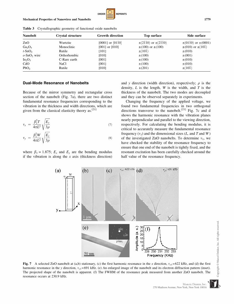
ORDER REPRINTS
Dual-Mode Resonance of Nanobelts
Because of the mirror symmetry and rectangular cross
section of the nanobelt (Fig 7a) there are two distinct
fundamental resonance frequencies corresponding to the
vibration in the thickness and width directions which are
given from the classical elasticity theory as[21]
nx frac14 b21T
4pL2
ffiffiffiffiffiffiEx
3r
seth7THORN
ny frac14 b21W
4pL2
ffiffiffiffiffiffiEy
3r
seth8THORN
where b1 = 1875 Ex and Ey are the bending modulus
if the vibration is along the x axis (thickness direction)
and y direction (width direction) respectively r is the
density L is the length W is the width and T is the
thickness of the nanobelt The two modes are decoupled
and they can be observed separately in experiments
Changing the frequency of the applied voltage we
found two fundamental frequencies in two orthogonal
directions transverse to the nanobelt[21] Fig 7c and d
shows the harmonic resonance with the vibration planes
nearly perpendicular and parallel to the viewing direction
respectively For calculating the bending modulus it is
critical to accurately measure the fundamental resonance
frequency (n1) and the dimensional sizes (L and T and W )
of the investigated ZnO nanobelts To determine n1 we
have checked the stability of the resonance frequency to
ensure that one end of the nanobelt is tightly fixed and the
resonant excitation has been carefully checked around the
half value of the resonance frequency
Fig 7 A selected ZnO nanobelt at (ab) stationary (c) the first harmonic resonance in the x direction nx1 =622 kHz and (d) the first
harmonic resonance in the y direction ny1 =691 kHz (e) An enlarged image of the nanobelt and its electron diffraction pattern (inset)
The projected shape of the nanobelt is apparent (f) The FWHM of the resonance peak measured from another ZnO nanobelt The
resonance occurs at 2309 kHz
Table 3 Crystallographic geometry of functional oxide nanobelts
Nanobelt Crystal structure Growth direction Top surface Side surface
ZnO Wurtzite [0001] or frac120110 plusmneth2110THORN or plusmneth2110THORN plusmneth0110THORN or plusmn(0001)
Ga2O3 Monoclinic [001] or [010] plusmn(100) or plusmn(100) plusmn(010) or plusmneth101THORNt-SnO2 Rutile [101] plusmneth101THORN plusmn(010)
o-SnO2 wire Orthorhombic [010] plusmn(100) plusmn(001)
In2O3 C-Rare earth [001] plusmn(100) plusmn(010)
CdO NaCl [001] plusmn(100) plusmn(010)
PbO2 Rutile [010] plusmn(201) plusmneth101THORN
Mechanical Properties of Nanowires and Nanobelts 1779
M
ORDER REPRINTS
ZnO nanobelts can be used as a force sensor Fig 8a
shows a selected ZnO nanobelt with a hooked end which
is equivalent to a cantilever with an integrated tip Be-
cause of the two transverse vibration modes of the
nanobelt resonance along two orthogonal directions has
been observed (Fig 8b and c) The two resonance modes
just correspond to the two modes of the tip operation
when the nanobelt-base cantilever is used as a force
sensor one is the tapping mode and the other is the
noncontact mode Thus the force sensor fabricated using
the ZnO nanobelts is versatile for applications on hard and
soft surfaces
Bending Modulus of Nanobelt
The geometrical parameters are the key for derivation of
the mechanical property from the measured resonance
frequencies The specimen holder is rotated about its axis
so that the nanobelt is aligned perpendicular to the
electron beam thus the real length (L) of the nanobelt can
be obtained The normal direction of the wide facet of the
nanobelt could be firstly determined by electron diffrac-
tion pattern which was frac122110 for the ZnO nanobelt Then
the nanobelt was tilted from its normal direction by
rotating the specimen holder and the tilting direction and
angle were determined by the corresponding electron
diffraction pattern As shown in the inset of Fig 7e the
electron beam direction is frac121100 The angle between
frac121100 and frac122110 is 30 ie the normal direction of the
wide facet of this nanobelt is 30 tilted from the direction
of the electron beam Using the projected dimension
measured from the TEM image (Fig 7e) the geometrical
parameters of this nanobelt are determined to be W = 28
nm and T = 19 nm Based on the experimentally measured
data the bending modulus of the ZnO nanobelts is
calculated using Eqs 7 and 8 The experimental results are
summarized in Table 4[21] The bending modulus of the
ZnO nanobelts was 52 GPa This value represents the
modulus that includes the scaling effect and geometrical
shape and it cannot be directly compared to the Youngrsquos
modulus of ZnO (c33 = 210 GPa c13 = 104 GPa)[22]
because the shape of the nanobelt and the anisotropic
structure of ZnO are convoluted in the measurement The
bending modulus measured by the resonance technique
however has excellent agreement with the elastic modu-
lus measured by nanoindentation for the same type of
nanobelts[23]
Although nanobelts of different sizes may have a slight
difference in bending modulus there is no obvious
difference if the calculation was done using either Eq 7
or Eq 8 The ratio of two fundamental frequencies ny1
nx1 is consistent with the aspect ratio WT as expected
from Eqs 7 and 8 because there is no significant dif-
ference between Ex and Ey
The resonance technique demonstrated here is very
sensitive to the structure of a nanowire Fig 9a and b
shows a silicon nanowire that has a Au tip but the Au
Fig 8 A selected ZnO nanobelt with a hooked end at (a)
stationary (b) resonance at 731 kHz in the plane almost parallel
to the viewing direction and (c) resonance at 474 kHz in the
place closely perpendicular to the viewing direction
Table 4 Bending modulus of the ZnO nanobelts Ex and Ey represents the bending modulus corresponding to the resonance along the
thickness and width directions respectively
Nanobelt
Length
L (mmm)
(plusmn005)
Width
W (nm) (plusmn1)
Thickness
T (nm) (plusmn1)
Fundamental frequency (kHz)
Bending modulus
(GPa)
WT nnx1 nny1 nny1nnx1 Ex Ey
1 825 55 33 17 232 373 16 466plusmn06 501plusmn06
2 473 28 19 15 396 576 14 443plusmn13 455plusmn29
3 407 31 20 16 662 958 14 563plusmn09 646plusmn23
4 890 44 39 11 210 231 11 379plusmn06 399plusmn12
1780 Mechanical Properties of Nanowires and Nanobelts
ORDER REPRINTS
particle is off the symmetric axis of the nanowire This
asymmetric structure results in two distinct resonance
along two perpendicular directions (Fig 9c and d) The
difference between the two resonance frequencies is re-
lated to the mass of the Au particle
THE HARDNESS OF A NANOBELTBY NANOINDENTATION
Nanoscale mechanical properties of individual zinc oxide
nanobelts were characterized by Nanoscope IIIa atomic
Fig 9 (a) A silicon nanowire with a gold particle at the tip showing (bc) two independent resonance along two perpen-
dicular directions
Fig 10 (a) Schematic of nanoindentation on ZnO by AFM tip (bc) AFM image of a nanobelt before and after being indented
showing plastic deformation on the surfaces (d) Hardness of ZnO and SnO2 nanobelts as a function of penetration during
nanoindentation (View this art in color at wwwdekkercom)
Mechanical Properties of Nanowires and Nanobelts 1781
M
ORDER REPRINTS
force microscope (AFM) (Fig 10a) and Hysitron Tribo-
Scope with homemade side-view CCD camera[23] The
prepared nanobelt sample was investigated by two means
one is by tapping mode of Nanoscope IIIa using a
diamond indenter tip with a radius of lt25 nm The other is
by STM mode of Hysitron TriboScope an add-on force
transducer from Hysitron Inc using a diamond cubic
corner tip with a radius of lt40 nm In either case in-
dividual nanobelts were imaged and then nanoindenta-
tions were made on the nanobelt using varied loads
(Fig 10b and c) After indentation the indent was imaged
in situ using the image mode of the AFM For nanoin-
dentations the hardness is normally defined as the maxi-
mum load divided by the projected area of the indenter in
contact with the sample at the maximum load Thus
H frac14 PMAX
AC
eth9THORN
where H PMAX and AC are the hardness maximum
applied load and projected contact area at the maximum
applied load respectively Because the indenter tip is not
rigid during indentation the elastic modulus cannot be
directly determined from the load vs the displacement
curve However the reduced elastic modulus can be
determined from the unloading portion of the curve by
the relation
Er frac14ffiffiffip
p
2 dP
dh 1ffiffiffiffiffi
Ac
p eth10THORN
where Er and dPdh are the reduced modulus and
experimentally measured stiffness respectively
Based on Eq 9 using load vs deflection curves
during nanoindentation the hardness of ZnO and SnO2
nanobelts was calculated as a function of indentation
penetration and the result is summarized in Fig 10d
The hardness of ZnO is lower than that in the SnO2
nanobelt Also it can be seen that the lower the
penetration of the nanoindentation the higher the
hardness of the nanobelt which is attributed to the strain
gradient effect (size effect) during nanoindentation for
most materials[24] The effective elastic modulus can also
be derived from the forcendashdisplacement curve and the
result is E = 45 GPa for ZnO in good agreement with
that from the resonance technique[21]
NANOBELTS AS NANOCANTILEVERS
The cantilever-based scanning probe microscopy (SPM)
technique is one of the most powerful approaches in
imaging manipulating and measuring nanoscale proper-
ties and phenomena The most conventional cantilever
used for SPM is based on silicon Si3N4 or SiC which is
fabricated by e-beam or optical lithography technique and
typically has a dimension of thickness of 100 nm width
of 5 mm and length of 50 mm Utilization of nano-
wire- and nanotube-based cantilevers can have several
advantages for SPM Carbon nanotubes can be grown
on the tip of a conventional cantilever and be used for
imaging surfaces with a large degree of abrupt variation in
surface morphology[2526] We demonstrate here the
manipulation of nanobelts by AFM and its potential as
nanocantilevers[27]
Manipulation of nanobelts is important for integrating
this structurally controlled nanomaterial with microelec-
trical mechanical system (MEMS) Using an AFM tip
a nanobelt can be manipulated into different shapes
(Fig 11) A ZnO nanobelt of 56 nm in width can be bent
for over 60 without breaking demonstrating extremely
high mechanical flexibility Further bending bent the
nanobelt into two segments This is a technique for cutting
a nanobelt into specific length
Combining MEMS technology with self-assembled
nanobelts we are able to produce cost-effective canti-
levers with much heightened sensitivity for a range of
Fig 11 A series of shape of a ZnO nanobelt created by
manipulation using an AFM tip showing deformation and
break-up (Image courtesy of MS Arnold Ph Avouris) (View
this art in color at wwwdekkercom)
1782 Mechanical Properties of Nanowires and Nanobelts
ORDER REPRINTS
devices and applications Force pressure mass thermal
biological and chemical sensors are all prospective
devices Semiconducting nanobelts are ideal candidates
for cantilever applications Structurally they are defect-
free single crystals providing excellent mechanical
properties The reduced dimensions of nanobelt cantile-
vers offer a significant increase in cantilever sensitivity
The cantilevers under consideration are simple in design
and practice Using a Dimension 3000 SPM in tapping
mode we have successfully lifted ZnO nanobelts from a
silicon substrate Capillary forces are responsible for the
adhesion strength between the AFM probe and the ZnO
nanobelts Combining the aforementioned techniques
with micromanipulation has led to the alignment of
individual ZnO nanobelts onto silicon chips (Fig 12)
The aligned ZnO cantilevers were manipulated to have a
range of lengths This exemplifies our ability to tune the
resonance frequency of each cantilever and thus modify
cantilevers for different applications such as tapping and
contact mode AFM The nanobelt-based nanocantilever
is 50ndash1000 times smaller than the conventional
cantilever Decreased size in microoptical mechanical
devices corresponds to increased sensitivity Combining
the aforementioned techniques with micromanipulation
has led to the horizontal alignment of individual ZnO
nanobelts onto silicon chips (Fig 12) This exempli-
fies our ability to tune the resonance frequency of each
cantilever and thus modify cantilevers for different
applications such as contact noncontact and tapping
mode AFM
THE WORK FUNCTION AT THE TIP OF ANANOBELT BY RESONANCE TECHNIQUE
The field-emission property for well-aligned ZnO nano-
wire arrays has been reported[28] demonstrating a promis-
ing application of semiconductor nanowires as field
emitters for flat panel display Following the Fowlerndash
Nordheim (FndashN) theory[29] an important physical quantity
in electron field emission is the surface work function
which is well documented for elemental materials For
the emitters such as ZnO nanowire arrays most of the
electrons are emitted from tips of the nanowires and it is
the local work function that matters to the properties of the
field emission However the work function measured
based on the FndashN theory is an average over the large scale
of emitting materials So it is necessary to measure the
local work function at the tip of an individual emitter Gao
et al[30] have measured the work function at the tips of
carbon nanotubes by an in situ TEM technique The
measurement relies on the mechanical resonance of the
carbon nanotube induced by an externally applied oscil-
lating voltage with tunable frequency
The measurement of the work function at the tip of a
single ZnO nanobelt was carried out in situ at 200 kV in a
Hitachi HF-2000 FEG TEM A specimen holder was built
for applying a voltage across a nanobelt and its counter
gold electrode The nanobelts to be used for measurements
are directly imaged under TEM Fig 13 is a setup for work
function measurement One end of the nanobelt was
electrically attached to a gold wire and the other end
Fig 12 Site-specific placement and alignment of ZnO nanobelts onto a silicon chip forming nanocantilever arrays The inset is an
enlarged SEM image of the third nanocantilever showing its shape the width of the cantilever was measured to be 525 nm
Mechanical Properties of Nanowires and Nanobelts 1783
M
ORDER REPRINTS
faces directly against the gold ball Because of the
difference in the surface work function between the ZnO
nanobelt and the counter Au ball a static charge Q0 exists
at the tip of the nanobelt to balance this potential
difference[31] The magnitude of Q0 is proportional to
the difference between the work function of the nanobelt
tip (NBT) and the Au electrode Q0 = a (fAufNBT)
where a is related to the geometry and distance between
the nanobelt and the electrode
The measurement is based on the mechanical reso-
nance of the nanobelt induced by an externally alternative
electric field Experimentally a constant voltage Vdc and
an oscillating voltage Vaccos2pft are applied onto the
nanobelt (Fig 13a) where f is the frequency and Vac is
the amplitude Thus the total induced charge on the
nanobelt is
Q frac14 Q0 thorn aeethVdc thorn Vac cos 2pftTHORN eth11THORN
The force acting on the nanobelt is proportional to the
square of the total charge on the nanobelt
F frac14 bfrac12Q0 thorn aeethVdc thorn Vac cos 2pftTHORN2
frac14 a2bffrac12ethfAu fNBT thorn eVdcTHORN2 thorn e2V2ac=2
thorn 2eVacethfAu fNBT thorn eVdcTHORN
cos 2pft thorn e2V2ac=2 cos 4pftg
eth12THORN
where b is a proportional constant In Eq 12 the first term
is constant and it causes a static deflection of the ZnO
nanobelt The second term is a linear term and the res-
onance occurs if the applied frequency f is tuned to the
intrinsic mechanical resonance frequency f0 of the ZnO
nanobelt The most important result of Eq 12 is that for
the linear term the resonance amplitude A of the nanobelt
is proportional to Vac(fAufNBT+eVdc)
The principle of the measurement is as follows We
first set Vdc = 0 and tune the frequency f to get the
mechanical resonance induced by the applied oscillat-
ing field Second under the resonance condition of
keeping f = f0 and Vac constant slowly change the mag-
nitude of Vdc from zero to a value Vdc0 that satisfies
fAufNBT+eVdc0 = 0 At this moment the resonance
amplitude A becomes zero although the external ac
voltage is still in effect Therefore the work function at the
tip of the ZnO nanobelt is fNBT = fAu+eVdc0 while
fAu = 51 eV Fig 14 is a plot of the vibration amplitude
A of the nanobelt as a function of the applied direct cur-
rent voltage Vdc from which the value for Vdc0 is
determined The work function of the ZnO nanobelts is
52 eV[32]
CONCLUSION
The property characterization of nanomaterials is chal-
lenged by their small-size structures because of the
difficulties in manipulation A typical example is the me-
chanical properties of individual 1-D nanostructures such
as nanotubes nanowires and nanobelts This chapter
reviews the experimental methods for measuring the
mechanical properties of 1-D nanostructures using a reso-
nance technique in TEM The static and dynamic pro-
perties of the 1-D nanostructures can be obtained by
applying controllable static and alternating electric fields
Fig 14 A plot of vibration amplitude of a ZnO nanobelt as a
function of the applied direct current voltage from which the
offset voltage Vdc0 =012 V
Fig 13 Experimental set-up for measuring the work function
at the tip of a ZnO nanobelt
1784 Mechanical Properties of Nanowires and Nanobelts
ORDER REPRINTS
The resonance of carbon nanotubes can be induced by
tuning the frequency of the applied voltage The technique
is powerful in such a way that it can directly correlate
the atomic-scale microstructure of the carbon nanotube
with its physical properties providing a one-to-one
correspondence in structurendashproperty characterization
Because of the rectangular cross section of the
nanobelt two fundamental resonance modes have been
observed corresponding to two orthogonal transverse
vibration directions showing the versatile applications
of nanobelts as nanocantilevers and nanoresonators The
bending modulus of the ZnO nanobelts was measured to
be 52 GPa Nanobelts have also been demonstrated as
ultrasmall nanocantilevers for sensor and possibly imag-
ing applications in AFM
ACKNOWLEDGMENTS
The results reviewed in this paper were partially contrib-
uted from my group members and collaborators Ruiping
Gao Xuedong Bai Scott Mao William Hughes and Enge
Wang to whom I am very grateful Research supported by
NSF NASA and NSFC
REFERENCES
1 Wang ZL Liu Y Zhang Z Handbook of
Nanophase and Nanostructured Materials 2002
Vols IndashIV Tsinghua University Press Beijing
Kluwer Academic Publisher New York
2 Wang ZL Hui C Electron Microscopy of
Nanotubes Kluwer Academic Publisher New York
2003
3 Poncharal P Wang ZL Ugarte D de Heer
WA Electrostatic deflections and electromechani-
cal resonances of carbon nanotubes Science 1999283 1513ndash1516
4 Wang ZL Poncharal P de Heer WA Nano-
measurements of individual carbon nanotubes by
in-situ TEM Pure Appl Chem 2000 72 209ndash
219
5 Gao RP Wang ZL Bai ZG de Heer WA
Dai LM Gao M Nanomechanics of aligned
carbon nanotube arrays Phys Rev Lett 2000 85622ndash635
6 Wang ZL Poncharal P de Heer WA Measur-
ing physical and mechanical properties of individual
carbon nanotubes by in-situ TEM J Phys Chem
Solids 2000 61 1025ndash1030
7 Meirovich L Elements of Vibration Analysis
McGraw-Hill New York 1986
8 Liu JZ Zheng QS Jiang Q Effect of ripping
mode on resonances of carbon nanotubes Phys Rev
Lett 2001 86 4843ndash4846
9 Wang ZL Dai ZR Bai ZG Gao RP Gole
JL Side-by-side silicon carbide-silica biaxial nano-
wires Synthesis structure and mechanical proper-
ties Appl Phys Lett 2000 77 3349ndash3351
10 Pan ZW Dai ZR Wang ZL Nanobelts of
semiconducting oxides Science 2001 291 1947ndash
1949
11 Wang ZL Pan ZW Dai ZR Semiconducting
Oxide Nanostructures US Patent No 6586095
July 1 2003
12 Dai ZR Pan ZW Wang ZL Gallium oxide
nanoribbons and nanosheets J Phys Chem B
2002 106 902ndash904
13 Dai ZR Pan ZW Wang ZL Growth and
structure evolution of novel tin oxide diskettes J
Am Chem Soc 2002 124 8673ndash8680
14 Kong XY Wang ZL Spontaneous polarization
and helical nanosprings of piezoelectric nanobelts
Nano Lett 2003 in press15 Wen XG Zhang WX Yang SH Dai ZR
Wang ZL Solution phase synthesis of Cu(OH)sub
2nanoribbons by coordination self-assembly using
Cusub 2S nanowires as precursors Nano Lett
2002 2 (12) 1397ndash1401
16 Li YB Bando Y Golberg D Kurashima K
Field emission from MoOsub 3nanobelts Appl
Phys Lett 2002 81 (26) 5048ndash5050
17 Zhou J Xu NS Deng SZ Chen J She JC
Wang ZL Large-area nanowire arrays of molyb-
denum and molybdenum oxides Synthesis and field
emission properties Adv Mater 2003 in press18 Li YB Bando Y Sato T Preparation of
network-like MgO nanobelts on Si substrate Chem
Phys Lett 2002 359 (1ndash2) 141ndash145
19 Liu J Cai J Son YC Gao QM Suib SL
Aindow M Magnesium manganese oxide nano-
ribbons Synthesis characterization and catalytic
application J Phys Chem B 2002 106 (38) 9761
20 Wen XG Zhang WX Yang SH Synthesis of
Cu- (OH)2 and CuO nanoribbon arrays on a copper
surface Langmuir 2003 19 5898ndash5903
21 Bai XD Wang EG Gao PX Wang ZL
Dual-mode mechanical resonance of individual
ZnO nanobelts Appl Phys Lett 2003 824806ndash4808
22 Carlotti G Socino G Petri A Verona E
Acoustic investigation of the elastic properties of
ZnO films Appl Phys Lett 1987 51 1889ndash1891
Mechanical Properties of Nanowires and Nanobelts 1785
M
ORDER REPRINTS
23 Mao SX Zhao MH Wang ZL Probing nano-
scale mechanical properties of individual semicon-
ducting nanobelt Appl Phys Lett 2002 83 993ndash
995
24 Duan DM Wu N Slaughter WS Mao SX
Length scale effect on mechanical behavior due to
strain gradient plasticity Mater Sci Eng A 2001A303 (1ndash2) 241ndash249
25 Yenilmez E Wang Q Chen RJ Wang D
Dai HJ Wafer scale production of carbon
nanotube scanning probe tips for atomic force
microscopy Appl Phys Lett 2002 80 (12)2225ndash2227
26 Dai HJ Hafner JH Rinzler AG Colbert
DT Smalley RE Nanotubes as nanoprobes in
scanning probe microscopy Nature 1996 384147ndash150
27 Hughes W Wang ZL Nanobelt as nanocantile-
ver Appl Phys Lett 2003 82 2886ndash2888
28 Lee CJ Lee TJ Lyu SC Zhang Y Ruh H
Lee HJ Field emission from well-aligned zinc
oxide nanowires grown at low temperature Appl
Phys Lett 2002 81 (19) 3648ndash3650
29 Fowler RH Nordherim LW Electron emission
in intense electric fields Proc R Soc Lond A
1928 119 (781) 173
30 Gao RP Pan ZW Wang ZL Work function at
the tips of multi-walled carbon nanotubes Appl
Phys Lett 2001 78 1757ndash1759
31 Kelvin L Philos Mag 1898 46 82
32 Bai XD Wang EG Gao PX Wang ZL
Measuring the work function at a nanobelt tip and at
a nanoparticle surface Nano Lett 2003 3 1147ndash
1150
1786 Mechanical Properties of Nanowires and Nanobelts
Request PermissionOrder Reprints
Reprints of this article can also be ordered at
httpwwwdekkercomservletproductDOI101081EENN120013387
Request Permission or Order Reprints Instantly
Interested in copying and sharing this article In most cases US Copyright Law requires that you get permission from the articlersquos rightsholder before using copyrighted content
All information and materials found in this article including but not limited to text trademarks patents logos graphics and images (the Materials) are the copyrighted works and other forms of intellectual property of Marcel Dekker Inc or its licensors All rights not expressly granted are reserved
Get permission to lawfully reproduce and distribute the Materials or order reprints quickly and painlessly Simply click on the Request Permission Order Reprints link below and follow the instructions Visit the US Copyright Office for information on Fair Use limitations of US copyright law Please refer to The Association of American Publishersrsquo (AAP) website for guidelines on Fair Use in the Classroom
The Materials are for your personal use only and cannot be reformatted reposted resold or distributed by electronic means or otherwise without permission from Marcel Dekker Inc Marcel Dekker Inc grants you the limited right to display the Materials only on your personal computer or personal wireless device and to copy and download single copies of such Materials provided that any copyright trademark or other notice appearing on such Materials is also retained by displayed copied or downloaded as part of the Materials and is not removed or obscured and provided you do not edit modify alter or enhance the Materials Please refer to our Website User Agreement for more details
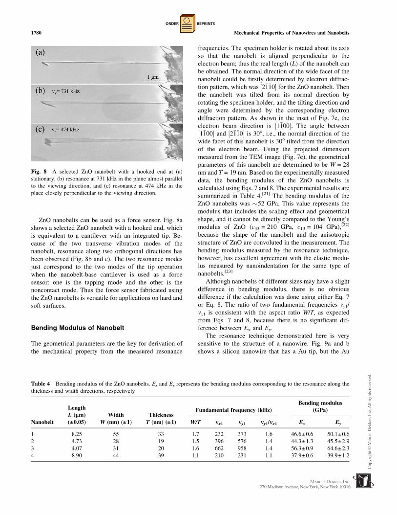
ORDER REPRINTS
ZnO nanobelts can be used as a force sensor Fig 8a
shows a selected ZnO nanobelt with a hooked end which
is equivalent to a cantilever with an integrated tip Be-
cause of the two transverse vibration modes of the
nanobelt resonance along two orthogonal directions has
been observed (Fig 8b and c) The two resonance modes
just correspond to the two modes of the tip operation
when the nanobelt-base cantilever is used as a force
sensor one is the tapping mode and the other is the
noncontact mode Thus the force sensor fabricated using
the ZnO nanobelts is versatile for applications on hard and
soft surfaces
Bending Modulus of Nanobelt
The geometrical parameters are the key for derivation of
the mechanical property from the measured resonance
frequencies The specimen holder is rotated about its axis
so that the nanobelt is aligned perpendicular to the
electron beam thus the real length (L) of the nanobelt can
be obtained The normal direction of the wide facet of the
nanobelt could be firstly determined by electron diffrac-
tion pattern which was frac122110 for the ZnO nanobelt Then
the nanobelt was tilted from its normal direction by
rotating the specimen holder and the tilting direction and
angle were determined by the corresponding electron
diffraction pattern As shown in the inset of Fig 7e the
electron beam direction is frac121100 The angle between
frac121100 and frac122110 is 30 ie the normal direction of the
wide facet of this nanobelt is 30 tilted from the direction
of the electron beam Using the projected dimension
measured from the TEM image (Fig 7e) the geometrical
parameters of this nanobelt are determined to be W = 28
nm and T = 19 nm Based on the experimentally measured
data the bending modulus of the ZnO nanobelts is
calculated using Eqs 7 and 8 The experimental results are
summarized in Table 4[21] The bending modulus of the
ZnO nanobelts was 52 GPa This value represents the
modulus that includes the scaling effect and geometrical
shape and it cannot be directly compared to the Youngrsquos
modulus of ZnO (c33 = 210 GPa c13 = 104 GPa)[22]
because the shape of the nanobelt and the anisotropic
structure of ZnO are convoluted in the measurement The
bending modulus measured by the resonance technique
however has excellent agreement with the elastic modu-
lus measured by nanoindentation for the same type of
nanobelts[23]
Although nanobelts of different sizes may have a slight
difference in bending modulus there is no obvious
difference if the calculation was done using either Eq 7
or Eq 8 The ratio of two fundamental frequencies ny1
nx1 is consistent with the aspect ratio WT as expected
from Eqs 7 and 8 because there is no significant dif-
ference between Ex and Ey
The resonance technique demonstrated here is very
sensitive to the structure of a nanowire Fig 9a and b
shows a silicon nanowire that has a Au tip but the Au
Fig 8 A selected ZnO nanobelt with a hooked end at (a)
stationary (b) resonance at 731 kHz in the plane almost parallel
to the viewing direction and (c) resonance at 474 kHz in the
place closely perpendicular to the viewing direction
Table 4 Bending modulus of the ZnO nanobelts Ex and Ey represents the bending modulus corresponding to the resonance along the
thickness and width directions respectively
Nanobelt
Length
L (mmm)
(plusmn005)
Width
W (nm) (plusmn1)
Thickness
T (nm) (plusmn1)
Fundamental frequency (kHz)
Bending modulus
(GPa)
WT nnx1 nny1 nny1nnx1 Ex Ey
1 825 55 33 17 232 373 16 466plusmn06 501plusmn06
2 473 28 19 15 396 576 14 443plusmn13 455plusmn29
3 407 31 20 16 662 958 14 563plusmn09 646plusmn23
4 890 44 39 11 210 231 11 379plusmn06 399plusmn12
1780 Mechanical Properties of Nanowires and Nanobelts
ORDER REPRINTS
particle is off the symmetric axis of the nanowire This
asymmetric structure results in two distinct resonance
along two perpendicular directions (Fig 9c and d) The
difference between the two resonance frequencies is re-
lated to the mass of the Au particle
THE HARDNESS OF A NANOBELTBY NANOINDENTATION
Nanoscale mechanical properties of individual zinc oxide
nanobelts were characterized by Nanoscope IIIa atomic
Fig 9 (a) A silicon nanowire with a gold particle at the tip showing (bc) two independent resonance along two perpen-
dicular directions
Fig 10 (a) Schematic of nanoindentation on ZnO by AFM tip (bc) AFM image of a nanobelt before and after being indented
showing plastic deformation on the surfaces (d) Hardness of ZnO and SnO2 nanobelts as a function of penetration during
nanoindentation (View this art in color at wwwdekkercom)
Mechanical Properties of Nanowires and Nanobelts 1781
M
ORDER REPRINTS
force microscope (AFM) (Fig 10a) and Hysitron Tribo-
Scope with homemade side-view CCD camera[23] The
prepared nanobelt sample was investigated by two means
one is by tapping mode of Nanoscope IIIa using a
diamond indenter tip with a radius of lt25 nm The other is
by STM mode of Hysitron TriboScope an add-on force
transducer from Hysitron Inc using a diamond cubic
corner tip with a radius of lt40 nm In either case in-
dividual nanobelts were imaged and then nanoindenta-
tions were made on the nanobelt using varied loads
(Fig 10b and c) After indentation the indent was imaged
in situ using the image mode of the AFM For nanoin-
dentations the hardness is normally defined as the maxi-
mum load divided by the projected area of the indenter in
contact with the sample at the maximum load Thus
H frac14 PMAX
AC
eth9THORN
where H PMAX and AC are the hardness maximum
applied load and projected contact area at the maximum
applied load respectively Because the indenter tip is not
rigid during indentation the elastic modulus cannot be
directly determined from the load vs the displacement
curve However the reduced elastic modulus can be
determined from the unloading portion of the curve by
the relation
Er frac14ffiffiffip
p
2 dP
dh 1ffiffiffiffiffi
Ac
p eth10THORN
where Er and dPdh are the reduced modulus and
experimentally measured stiffness respectively
Based on Eq 9 using load vs deflection curves
during nanoindentation the hardness of ZnO and SnO2
nanobelts was calculated as a function of indentation
penetration and the result is summarized in Fig 10d
The hardness of ZnO is lower than that in the SnO2
nanobelt Also it can be seen that the lower the
penetration of the nanoindentation the higher the
hardness of the nanobelt which is attributed to the strain
gradient effect (size effect) during nanoindentation for
most materials[24] The effective elastic modulus can also
be derived from the forcendashdisplacement curve and the
result is E = 45 GPa for ZnO in good agreement with
that from the resonance technique[21]
NANOBELTS AS NANOCANTILEVERS
The cantilever-based scanning probe microscopy (SPM)
technique is one of the most powerful approaches in
imaging manipulating and measuring nanoscale proper-
ties and phenomena The most conventional cantilever
used for SPM is based on silicon Si3N4 or SiC which is
fabricated by e-beam or optical lithography technique and
typically has a dimension of thickness of 100 nm width
of 5 mm and length of 50 mm Utilization of nano-
wire- and nanotube-based cantilevers can have several
advantages for SPM Carbon nanotubes can be grown
on the tip of a conventional cantilever and be used for
imaging surfaces with a large degree of abrupt variation in
surface morphology[2526] We demonstrate here the
manipulation of nanobelts by AFM and its potential as
nanocantilevers[27]
Manipulation of nanobelts is important for integrating
this structurally controlled nanomaterial with microelec-
trical mechanical system (MEMS) Using an AFM tip
a nanobelt can be manipulated into different shapes
(Fig 11) A ZnO nanobelt of 56 nm in width can be bent
for over 60 without breaking demonstrating extremely
high mechanical flexibility Further bending bent the
nanobelt into two segments This is a technique for cutting
a nanobelt into specific length
Combining MEMS technology with self-assembled
nanobelts we are able to produce cost-effective canti-
levers with much heightened sensitivity for a range of
Fig 11 A series of shape of a ZnO nanobelt created by
manipulation using an AFM tip showing deformation and
break-up (Image courtesy of MS Arnold Ph Avouris) (View
this art in color at wwwdekkercom)
1782 Mechanical Properties of Nanowires and Nanobelts
ORDER REPRINTS
devices and applications Force pressure mass thermal
biological and chemical sensors are all prospective
devices Semiconducting nanobelts are ideal candidates
for cantilever applications Structurally they are defect-
free single crystals providing excellent mechanical
properties The reduced dimensions of nanobelt cantile-
vers offer a significant increase in cantilever sensitivity
The cantilevers under consideration are simple in design
and practice Using a Dimension 3000 SPM in tapping
mode we have successfully lifted ZnO nanobelts from a
silicon substrate Capillary forces are responsible for the
adhesion strength between the AFM probe and the ZnO
nanobelts Combining the aforementioned techniques
with micromanipulation has led to the alignment of
individual ZnO nanobelts onto silicon chips (Fig 12)
The aligned ZnO cantilevers were manipulated to have a
range of lengths This exemplifies our ability to tune the
resonance frequency of each cantilever and thus modify
cantilevers for different applications such as tapping and
contact mode AFM The nanobelt-based nanocantilever
is 50ndash1000 times smaller than the conventional
cantilever Decreased size in microoptical mechanical
devices corresponds to increased sensitivity Combining
the aforementioned techniques with micromanipulation
has led to the horizontal alignment of individual ZnO
nanobelts onto silicon chips (Fig 12) This exempli-
fies our ability to tune the resonance frequency of each
cantilever and thus modify cantilevers for different
applications such as contact noncontact and tapping
mode AFM
THE WORK FUNCTION AT THE TIP OF ANANOBELT BY RESONANCE TECHNIQUE
The field-emission property for well-aligned ZnO nano-
wire arrays has been reported[28] demonstrating a promis-
ing application of semiconductor nanowires as field
emitters for flat panel display Following the Fowlerndash
Nordheim (FndashN) theory[29] an important physical quantity
in electron field emission is the surface work function
which is well documented for elemental materials For
the emitters such as ZnO nanowire arrays most of the
electrons are emitted from tips of the nanowires and it is
the local work function that matters to the properties of the
field emission However the work function measured
based on the FndashN theory is an average over the large scale
of emitting materials So it is necessary to measure the
local work function at the tip of an individual emitter Gao
et al[30] have measured the work function at the tips of
carbon nanotubes by an in situ TEM technique The
measurement relies on the mechanical resonance of the
carbon nanotube induced by an externally applied oscil-
lating voltage with tunable frequency
The measurement of the work function at the tip of a
single ZnO nanobelt was carried out in situ at 200 kV in a
Hitachi HF-2000 FEG TEM A specimen holder was built
for applying a voltage across a nanobelt and its counter
gold electrode The nanobelts to be used for measurements
are directly imaged under TEM Fig 13 is a setup for work
function measurement One end of the nanobelt was
electrically attached to a gold wire and the other end
Fig 12 Site-specific placement and alignment of ZnO nanobelts onto a silicon chip forming nanocantilever arrays The inset is an
enlarged SEM image of the third nanocantilever showing its shape the width of the cantilever was measured to be 525 nm
Mechanical Properties of Nanowires and Nanobelts 1783
M
ORDER REPRINTS
faces directly against the gold ball Because of the
difference in the surface work function between the ZnO
nanobelt and the counter Au ball a static charge Q0 exists
at the tip of the nanobelt to balance this potential
difference[31] The magnitude of Q0 is proportional to
the difference between the work function of the nanobelt
tip (NBT) and the Au electrode Q0 = a (fAufNBT)
where a is related to the geometry and distance between
the nanobelt and the electrode
The measurement is based on the mechanical reso-
nance of the nanobelt induced by an externally alternative
electric field Experimentally a constant voltage Vdc and
an oscillating voltage Vaccos2pft are applied onto the
nanobelt (Fig 13a) where f is the frequency and Vac is
the amplitude Thus the total induced charge on the
nanobelt is
Q frac14 Q0 thorn aeethVdc thorn Vac cos 2pftTHORN eth11THORN
The force acting on the nanobelt is proportional to the
square of the total charge on the nanobelt
F frac14 bfrac12Q0 thorn aeethVdc thorn Vac cos 2pftTHORN2
frac14 a2bffrac12ethfAu fNBT thorn eVdcTHORN2 thorn e2V2ac=2
thorn 2eVacethfAu fNBT thorn eVdcTHORN
cos 2pft thorn e2V2ac=2 cos 4pftg
eth12THORN
where b is a proportional constant In Eq 12 the first term
is constant and it causes a static deflection of the ZnO
nanobelt The second term is a linear term and the res-
onance occurs if the applied frequency f is tuned to the
intrinsic mechanical resonance frequency f0 of the ZnO
nanobelt The most important result of Eq 12 is that for
the linear term the resonance amplitude A of the nanobelt
is proportional to Vac(fAufNBT+eVdc)
The principle of the measurement is as follows We
first set Vdc = 0 and tune the frequency f to get the
mechanical resonance induced by the applied oscillat-
ing field Second under the resonance condition of
keeping f = f0 and Vac constant slowly change the mag-
nitude of Vdc from zero to a value Vdc0 that satisfies
fAufNBT+eVdc0 = 0 At this moment the resonance
amplitude A becomes zero although the external ac
voltage is still in effect Therefore the work function at the
tip of the ZnO nanobelt is fNBT = fAu+eVdc0 while
fAu = 51 eV Fig 14 is a plot of the vibration amplitude
A of the nanobelt as a function of the applied direct cur-
rent voltage Vdc from which the value for Vdc0 is
determined The work function of the ZnO nanobelts is
52 eV[32]
CONCLUSION
The property characterization of nanomaterials is chal-
lenged by their small-size structures because of the
difficulties in manipulation A typical example is the me-
chanical properties of individual 1-D nanostructures such
as nanotubes nanowires and nanobelts This chapter
reviews the experimental methods for measuring the
mechanical properties of 1-D nanostructures using a reso-
nance technique in TEM The static and dynamic pro-
perties of the 1-D nanostructures can be obtained by
applying controllable static and alternating electric fields
Fig 14 A plot of vibration amplitude of a ZnO nanobelt as a
function of the applied direct current voltage from which the
offset voltage Vdc0 =012 V
Fig 13 Experimental set-up for measuring the work function
at the tip of a ZnO nanobelt
1784 Mechanical Properties of Nanowires and Nanobelts
ORDER REPRINTS
The resonance of carbon nanotubes can be induced by
tuning the frequency of the applied voltage The technique
is powerful in such a way that it can directly correlate
the atomic-scale microstructure of the carbon nanotube
with its physical properties providing a one-to-one
correspondence in structurendashproperty characterization
Because of the rectangular cross section of the
nanobelt two fundamental resonance modes have been
observed corresponding to two orthogonal transverse
vibration directions showing the versatile applications
of nanobelts as nanocantilevers and nanoresonators The
bending modulus of the ZnO nanobelts was measured to
be 52 GPa Nanobelts have also been demonstrated as
ultrasmall nanocantilevers for sensor and possibly imag-
ing applications in AFM
ACKNOWLEDGMENTS
The results reviewed in this paper were partially contrib-
uted from my group members and collaborators Ruiping
Gao Xuedong Bai Scott Mao William Hughes and Enge
Wang to whom I am very grateful Research supported by
NSF NASA and NSFC
REFERENCES
1 Wang ZL Liu Y Zhang Z Handbook of
Nanophase and Nanostructured Materials 2002
Vols IndashIV Tsinghua University Press Beijing
Kluwer Academic Publisher New York
2 Wang ZL Hui C Electron Microscopy of
Nanotubes Kluwer Academic Publisher New York
2003
3 Poncharal P Wang ZL Ugarte D de Heer
WA Electrostatic deflections and electromechani-
cal resonances of carbon nanotubes Science 1999283 1513ndash1516
4 Wang ZL Poncharal P de Heer WA Nano-
measurements of individual carbon nanotubes by
in-situ TEM Pure Appl Chem 2000 72 209ndash
219
5 Gao RP Wang ZL Bai ZG de Heer WA
Dai LM Gao M Nanomechanics of aligned
carbon nanotube arrays Phys Rev Lett 2000 85622ndash635
6 Wang ZL Poncharal P de Heer WA Measur-
ing physical and mechanical properties of individual
carbon nanotubes by in-situ TEM J Phys Chem
Solids 2000 61 1025ndash1030
7 Meirovich L Elements of Vibration Analysis
McGraw-Hill New York 1986
8 Liu JZ Zheng QS Jiang Q Effect of ripping
mode on resonances of carbon nanotubes Phys Rev
Lett 2001 86 4843ndash4846
9 Wang ZL Dai ZR Bai ZG Gao RP Gole
JL Side-by-side silicon carbide-silica biaxial nano-
wires Synthesis structure and mechanical proper-
ties Appl Phys Lett 2000 77 3349ndash3351
10 Pan ZW Dai ZR Wang ZL Nanobelts of
semiconducting oxides Science 2001 291 1947ndash
1949
11 Wang ZL Pan ZW Dai ZR Semiconducting
Oxide Nanostructures US Patent No 6586095
July 1 2003
12 Dai ZR Pan ZW Wang ZL Gallium oxide
nanoribbons and nanosheets J Phys Chem B
2002 106 902ndash904
13 Dai ZR Pan ZW Wang ZL Growth and
structure evolution of novel tin oxide diskettes J
Am Chem Soc 2002 124 8673ndash8680
14 Kong XY Wang ZL Spontaneous polarization
and helical nanosprings of piezoelectric nanobelts
Nano Lett 2003 in press15 Wen XG Zhang WX Yang SH Dai ZR
Wang ZL Solution phase synthesis of Cu(OH)sub
2nanoribbons by coordination self-assembly using
Cusub 2S nanowires as precursors Nano Lett
2002 2 (12) 1397ndash1401
16 Li YB Bando Y Golberg D Kurashima K
Field emission from MoOsub 3nanobelts Appl
Phys Lett 2002 81 (26) 5048ndash5050
17 Zhou J Xu NS Deng SZ Chen J She JC
Wang ZL Large-area nanowire arrays of molyb-
denum and molybdenum oxides Synthesis and field
emission properties Adv Mater 2003 in press18 Li YB Bando Y Sato T Preparation of
network-like MgO nanobelts on Si substrate Chem
Phys Lett 2002 359 (1ndash2) 141ndash145
19 Liu J Cai J Son YC Gao QM Suib SL
Aindow M Magnesium manganese oxide nano-
ribbons Synthesis characterization and catalytic
application J Phys Chem B 2002 106 (38) 9761
20 Wen XG Zhang WX Yang SH Synthesis of
Cu- (OH)2 and CuO nanoribbon arrays on a copper
surface Langmuir 2003 19 5898ndash5903
21 Bai XD Wang EG Gao PX Wang ZL
Dual-mode mechanical resonance of individual
ZnO nanobelts Appl Phys Lett 2003 824806ndash4808
22 Carlotti G Socino G Petri A Verona E
Acoustic investigation of the elastic properties of
ZnO films Appl Phys Lett 1987 51 1889ndash1891
Mechanical Properties of Nanowires and Nanobelts 1785
M
ORDER REPRINTS
23 Mao SX Zhao MH Wang ZL Probing nano-
scale mechanical properties of individual semicon-
ducting nanobelt Appl Phys Lett 2002 83 993ndash
995
24 Duan DM Wu N Slaughter WS Mao SX
Length scale effect on mechanical behavior due to
strain gradient plasticity Mater Sci Eng A 2001A303 (1ndash2) 241ndash249
25 Yenilmez E Wang Q Chen RJ Wang D
Dai HJ Wafer scale production of carbon
nanotube scanning probe tips for atomic force
microscopy Appl Phys Lett 2002 80 (12)2225ndash2227
26 Dai HJ Hafner JH Rinzler AG Colbert
DT Smalley RE Nanotubes as nanoprobes in
scanning probe microscopy Nature 1996 384147ndash150
27 Hughes W Wang ZL Nanobelt as nanocantile-
ver Appl Phys Lett 2003 82 2886ndash2888
28 Lee CJ Lee TJ Lyu SC Zhang Y Ruh H
Lee HJ Field emission from well-aligned zinc
oxide nanowires grown at low temperature Appl
Phys Lett 2002 81 (19) 3648ndash3650
29 Fowler RH Nordherim LW Electron emission
in intense electric fields Proc R Soc Lond A
1928 119 (781) 173
30 Gao RP Pan ZW Wang ZL Work function at
the tips of multi-walled carbon nanotubes Appl
Phys Lett 2001 78 1757ndash1759
31 Kelvin L Philos Mag 1898 46 82
32 Bai XD Wang EG Gao PX Wang ZL
Measuring the work function at a nanobelt tip and at
a nanoparticle surface Nano Lett 2003 3 1147ndash
1150
1786 Mechanical Properties of Nanowires and Nanobelts
Request PermissionOrder Reprints
Reprints of this article can also be ordered at
httpwwwdekkercomservletproductDOI101081EENN120013387
Request Permission or Order Reprints Instantly
Interested in copying and sharing this article In most cases US Copyright Law requires that you get permission from the articlersquos rightsholder before using copyrighted content
All information and materials found in this article including but not limited to text trademarks patents logos graphics and images (the Materials) are the copyrighted works and other forms of intellectual property of Marcel Dekker Inc or its licensors All rights not expressly granted are reserved
Get permission to lawfully reproduce and distribute the Materials or order reprints quickly and painlessly Simply click on the Request Permission Order Reprints link below and follow the instructions Visit the US Copyright Office for information on Fair Use limitations of US copyright law Please refer to The Association of American Publishersrsquo (AAP) website for guidelines on Fair Use in the Classroom
The Materials are for your personal use only and cannot be reformatted reposted resold or distributed by electronic means or otherwise without permission from Marcel Dekker Inc Marcel Dekker Inc grants you the limited right to display the Materials only on your personal computer or personal wireless device and to copy and download single copies of such Materials provided that any copyright trademark or other notice appearing on such Materials is also retained by displayed copied or downloaded as part of the Materials and is not removed or obscured and provided you do not edit modify alter or enhance the Materials Please refer to our Website User Agreement for more details
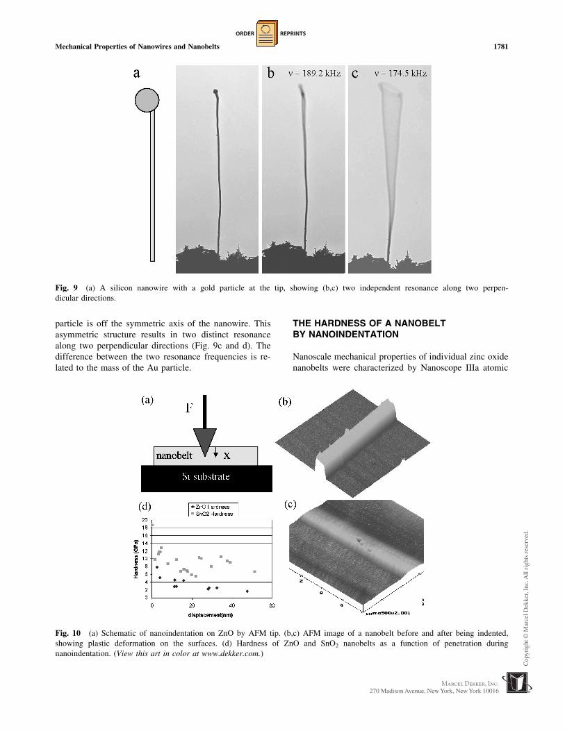
ORDER REPRINTS
particle is off the symmetric axis of the nanowire This
asymmetric structure results in two distinct resonance
along two perpendicular directions (Fig 9c and d) The
difference between the two resonance frequencies is re-
lated to the mass of the Au particle
THE HARDNESS OF A NANOBELTBY NANOINDENTATION
Nanoscale mechanical properties of individual zinc oxide
nanobelts were characterized by Nanoscope IIIa atomic
Fig 9 (a) A silicon nanowire with a gold particle at the tip showing (bc) two independent resonance along two perpen-
dicular directions
Fig 10 (a) Schematic of nanoindentation on ZnO by AFM tip (bc) AFM image of a nanobelt before and after being indented
showing plastic deformation on the surfaces (d) Hardness of ZnO and SnO2 nanobelts as a function of penetration during
nanoindentation (View this art in color at wwwdekkercom)
Mechanical Properties of Nanowires and Nanobelts 1781
M
ORDER REPRINTS
force microscope (AFM) (Fig 10a) and Hysitron Tribo-
Scope with homemade side-view CCD camera[23] The
prepared nanobelt sample was investigated by two means
one is by tapping mode of Nanoscope IIIa using a
diamond indenter tip with a radius of lt25 nm The other is
by STM mode of Hysitron TriboScope an add-on force
transducer from Hysitron Inc using a diamond cubic
corner tip with a radius of lt40 nm In either case in-
dividual nanobelts were imaged and then nanoindenta-
tions were made on the nanobelt using varied loads
(Fig 10b and c) After indentation the indent was imaged
in situ using the image mode of the AFM For nanoin-
dentations the hardness is normally defined as the maxi-
mum load divided by the projected area of the indenter in
contact with the sample at the maximum load Thus
H frac14 PMAX
AC
eth9THORN
where H PMAX and AC are the hardness maximum
applied load and projected contact area at the maximum
applied load respectively Because the indenter tip is not
rigid during indentation the elastic modulus cannot be
directly determined from the load vs the displacement
curve However the reduced elastic modulus can be
determined from the unloading portion of the curve by
the relation
Er frac14ffiffiffip
p
2 dP
dh 1ffiffiffiffiffi
Ac
p eth10THORN
where Er and dPdh are the reduced modulus and
experimentally measured stiffness respectively
Based on Eq 9 using load vs deflection curves
during nanoindentation the hardness of ZnO and SnO2
nanobelts was calculated as a function of indentation
penetration and the result is summarized in Fig 10d
The hardness of ZnO is lower than that in the SnO2
nanobelt Also it can be seen that the lower the
penetration of the nanoindentation the higher the
hardness of the nanobelt which is attributed to the strain
gradient effect (size effect) during nanoindentation for
most materials[24] The effective elastic modulus can also
be derived from the forcendashdisplacement curve and the
result is E = 45 GPa for ZnO in good agreement with
that from the resonance technique[21]
NANOBELTS AS NANOCANTILEVERS
The cantilever-based scanning probe microscopy (SPM)
technique is one of the most powerful approaches in
imaging manipulating and measuring nanoscale proper-
ties and phenomena The most conventional cantilever
used for SPM is based on silicon Si3N4 or SiC which is
fabricated by e-beam or optical lithography technique and
typically has a dimension of thickness of 100 nm width
of 5 mm and length of 50 mm Utilization of nano-
wire- and nanotube-based cantilevers can have several
advantages for SPM Carbon nanotubes can be grown
on the tip of a conventional cantilever and be used for
imaging surfaces with a large degree of abrupt variation in
surface morphology[2526] We demonstrate here the
manipulation of nanobelts by AFM and its potential as
nanocantilevers[27]
Manipulation of nanobelts is important for integrating
this structurally controlled nanomaterial with microelec-
trical mechanical system (MEMS) Using an AFM tip
a nanobelt can be manipulated into different shapes
(Fig 11) A ZnO nanobelt of 56 nm in width can be bent
for over 60 without breaking demonstrating extremely
high mechanical flexibility Further bending bent the
nanobelt into two segments This is a technique for cutting
a nanobelt into specific length
Combining MEMS technology with self-assembled
nanobelts we are able to produce cost-effective canti-
levers with much heightened sensitivity for a range of
Fig 11 A series of shape of a ZnO nanobelt created by
manipulation using an AFM tip showing deformation and
break-up (Image courtesy of MS Arnold Ph Avouris) (View
this art in color at wwwdekkercom)
1782 Mechanical Properties of Nanowires and Nanobelts
ORDER REPRINTS
devices and applications Force pressure mass thermal
biological and chemical sensors are all prospective
devices Semiconducting nanobelts are ideal candidates
for cantilever applications Structurally they are defect-
free single crystals providing excellent mechanical
properties The reduced dimensions of nanobelt cantile-
vers offer a significant increase in cantilever sensitivity
The cantilevers under consideration are simple in design
and practice Using a Dimension 3000 SPM in tapping
mode we have successfully lifted ZnO nanobelts from a
silicon substrate Capillary forces are responsible for the
adhesion strength between the AFM probe and the ZnO
nanobelts Combining the aforementioned techniques
with micromanipulation has led to the alignment of
individual ZnO nanobelts onto silicon chips (Fig 12)
The aligned ZnO cantilevers were manipulated to have a
range of lengths This exemplifies our ability to tune the
resonance frequency of each cantilever and thus modify
cantilevers for different applications such as tapping and
contact mode AFM The nanobelt-based nanocantilever
is 50ndash1000 times smaller than the conventional
cantilever Decreased size in microoptical mechanical
devices corresponds to increased sensitivity Combining
the aforementioned techniques with micromanipulation
has led to the horizontal alignment of individual ZnO
nanobelts onto silicon chips (Fig 12) This exempli-
fies our ability to tune the resonance frequency of each
cantilever and thus modify cantilevers for different
applications such as contact noncontact and tapping
mode AFM
THE WORK FUNCTION AT THE TIP OF ANANOBELT BY RESONANCE TECHNIQUE
The field-emission property for well-aligned ZnO nano-
wire arrays has been reported[28] demonstrating a promis-
ing application of semiconductor nanowires as field
emitters for flat panel display Following the Fowlerndash
Nordheim (FndashN) theory[29] an important physical quantity
in electron field emission is the surface work function
which is well documented for elemental materials For
the emitters such as ZnO nanowire arrays most of the
electrons are emitted from tips of the nanowires and it is
the local work function that matters to the properties of the
field emission However the work function measured
based on the FndashN theory is an average over the large scale
of emitting materials So it is necessary to measure the
local work function at the tip of an individual emitter Gao
et al[30] have measured the work function at the tips of
carbon nanotubes by an in situ TEM technique The
measurement relies on the mechanical resonance of the
carbon nanotube induced by an externally applied oscil-
lating voltage with tunable frequency
The measurement of the work function at the tip of a
single ZnO nanobelt was carried out in situ at 200 kV in a
Hitachi HF-2000 FEG TEM A specimen holder was built
for applying a voltage across a nanobelt and its counter
gold electrode The nanobelts to be used for measurements
are directly imaged under TEM Fig 13 is a setup for work
function measurement One end of the nanobelt was
electrically attached to a gold wire and the other end
Fig 12 Site-specific placement and alignment of ZnO nanobelts onto a silicon chip forming nanocantilever arrays The inset is an
enlarged SEM image of the third nanocantilever showing its shape the width of the cantilever was measured to be 525 nm
Mechanical Properties of Nanowires and Nanobelts 1783
M
ORDER REPRINTS
faces directly against the gold ball Because of the
difference in the surface work function between the ZnO
nanobelt and the counter Au ball a static charge Q0 exists
at the tip of the nanobelt to balance this potential
difference[31] The magnitude of Q0 is proportional to
the difference between the work function of the nanobelt
tip (NBT) and the Au electrode Q0 = a (fAufNBT)
where a is related to the geometry and distance between
the nanobelt and the electrode
The measurement is based on the mechanical reso-
nance of the nanobelt induced by an externally alternative
electric field Experimentally a constant voltage Vdc and
an oscillating voltage Vaccos2pft are applied onto the
nanobelt (Fig 13a) where f is the frequency and Vac is
the amplitude Thus the total induced charge on the
nanobelt is
Q frac14 Q0 thorn aeethVdc thorn Vac cos 2pftTHORN eth11THORN
The force acting on the nanobelt is proportional to the
square of the total charge on the nanobelt
F frac14 bfrac12Q0 thorn aeethVdc thorn Vac cos 2pftTHORN2
frac14 a2bffrac12ethfAu fNBT thorn eVdcTHORN2 thorn e2V2ac=2
thorn 2eVacethfAu fNBT thorn eVdcTHORN
cos 2pft thorn e2V2ac=2 cos 4pftg
eth12THORN
where b is a proportional constant In Eq 12 the first term
is constant and it causes a static deflection of the ZnO
nanobelt The second term is a linear term and the res-
onance occurs if the applied frequency f is tuned to the
intrinsic mechanical resonance frequency f0 of the ZnO
nanobelt The most important result of Eq 12 is that for
the linear term the resonance amplitude A of the nanobelt
is proportional to Vac(fAufNBT+eVdc)
The principle of the measurement is as follows We
first set Vdc = 0 and tune the frequency f to get the
mechanical resonance induced by the applied oscillat-
ing field Second under the resonance condition of
keeping f = f0 and Vac constant slowly change the mag-
nitude of Vdc from zero to a value Vdc0 that satisfies
fAufNBT+eVdc0 = 0 At this moment the resonance
amplitude A becomes zero although the external ac
voltage is still in effect Therefore the work function at the
tip of the ZnO nanobelt is fNBT = fAu+eVdc0 while
fAu = 51 eV Fig 14 is a plot of the vibration amplitude
A of the nanobelt as a function of the applied direct cur-
rent voltage Vdc from which the value for Vdc0 is
determined The work function of the ZnO nanobelts is
52 eV[32]
CONCLUSION
The property characterization of nanomaterials is chal-
lenged by their small-size structures because of the
difficulties in manipulation A typical example is the me-
chanical properties of individual 1-D nanostructures such
as nanotubes nanowires and nanobelts This chapter
reviews the experimental methods for measuring the
mechanical properties of 1-D nanostructures using a reso-
nance technique in TEM The static and dynamic pro-
perties of the 1-D nanostructures can be obtained by
applying controllable static and alternating electric fields
Fig 14 A plot of vibration amplitude of a ZnO nanobelt as a
function of the applied direct current voltage from which the
offset voltage Vdc0 =012 V
Fig 13 Experimental set-up for measuring the work function
at the tip of a ZnO nanobelt
1784 Mechanical Properties of Nanowires and Nanobelts
ORDER REPRINTS
The resonance of carbon nanotubes can be induced by
tuning the frequency of the applied voltage The technique
is powerful in such a way that it can directly correlate
the atomic-scale microstructure of the carbon nanotube
with its physical properties providing a one-to-one
correspondence in structurendashproperty characterization
Because of the rectangular cross section of the
nanobelt two fundamental resonance modes have been
observed corresponding to two orthogonal transverse
vibration directions showing the versatile applications
of nanobelts as nanocantilevers and nanoresonators The
bending modulus of the ZnO nanobelts was measured to
be 52 GPa Nanobelts have also been demonstrated as
ultrasmall nanocantilevers for sensor and possibly imag-
ing applications in AFM
ACKNOWLEDGMENTS
The results reviewed in this paper were partially contrib-
uted from my group members and collaborators Ruiping
Gao Xuedong Bai Scott Mao William Hughes and Enge
Wang to whom I am very grateful Research supported by
NSF NASA and NSFC
REFERENCES
1 Wang ZL Liu Y Zhang Z Handbook of
Nanophase and Nanostructured Materials 2002
Vols IndashIV Tsinghua University Press Beijing
Kluwer Academic Publisher New York
2 Wang ZL Hui C Electron Microscopy of
Nanotubes Kluwer Academic Publisher New York
2003
3 Poncharal P Wang ZL Ugarte D de Heer
WA Electrostatic deflections and electromechani-
cal resonances of carbon nanotubes Science 1999283 1513ndash1516
4 Wang ZL Poncharal P de Heer WA Nano-
measurements of individual carbon nanotubes by
in-situ TEM Pure Appl Chem 2000 72 209ndash
219
5 Gao RP Wang ZL Bai ZG de Heer WA
Dai LM Gao M Nanomechanics of aligned
carbon nanotube arrays Phys Rev Lett 2000 85622ndash635
6 Wang ZL Poncharal P de Heer WA Measur-
ing physical and mechanical properties of individual
carbon nanotubes by in-situ TEM J Phys Chem
Solids 2000 61 1025ndash1030
7 Meirovich L Elements of Vibration Analysis
McGraw-Hill New York 1986
8 Liu JZ Zheng QS Jiang Q Effect of ripping
mode on resonances of carbon nanotubes Phys Rev
Lett 2001 86 4843ndash4846
9 Wang ZL Dai ZR Bai ZG Gao RP Gole
JL Side-by-side silicon carbide-silica biaxial nano-
wires Synthesis structure and mechanical proper-
ties Appl Phys Lett 2000 77 3349ndash3351
10 Pan ZW Dai ZR Wang ZL Nanobelts of
semiconducting oxides Science 2001 291 1947ndash
1949
11 Wang ZL Pan ZW Dai ZR Semiconducting
Oxide Nanostructures US Patent No 6586095
July 1 2003
12 Dai ZR Pan ZW Wang ZL Gallium oxide
nanoribbons and nanosheets J Phys Chem B
2002 106 902ndash904
13 Dai ZR Pan ZW Wang ZL Growth and
structure evolution of novel tin oxide diskettes J
Am Chem Soc 2002 124 8673ndash8680
14 Kong XY Wang ZL Spontaneous polarization
and helical nanosprings of piezoelectric nanobelts
Nano Lett 2003 in press15 Wen XG Zhang WX Yang SH Dai ZR
Wang ZL Solution phase synthesis of Cu(OH)sub
2nanoribbons by coordination self-assembly using
Cusub 2S nanowires as precursors Nano Lett
2002 2 (12) 1397ndash1401
16 Li YB Bando Y Golberg D Kurashima K
Field emission from MoOsub 3nanobelts Appl
Phys Lett 2002 81 (26) 5048ndash5050
17 Zhou J Xu NS Deng SZ Chen J She JC
Wang ZL Large-area nanowire arrays of molyb-
denum and molybdenum oxides Synthesis and field
emission properties Adv Mater 2003 in press18 Li YB Bando Y Sato T Preparation of
network-like MgO nanobelts on Si substrate Chem
Phys Lett 2002 359 (1ndash2) 141ndash145
19 Liu J Cai J Son YC Gao QM Suib SL
Aindow M Magnesium manganese oxide nano-
ribbons Synthesis characterization and catalytic
application J Phys Chem B 2002 106 (38) 9761
20 Wen XG Zhang WX Yang SH Synthesis of
Cu- (OH)2 and CuO nanoribbon arrays on a copper
surface Langmuir 2003 19 5898ndash5903
21 Bai XD Wang EG Gao PX Wang ZL
Dual-mode mechanical resonance of individual
ZnO nanobelts Appl Phys Lett 2003 824806ndash4808
22 Carlotti G Socino G Petri A Verona E
Acoustic investigation of the elastic properties of
ZnO films Appl Phys Lett 1987 51 1889ndash1891
Mechanical Properties of Nanowires and Nanobelts 1785
M
ORDER REPRINTS
23 Mao SX Zhao MH Wang ZL Probing nano-
scale mechanical properties of individual semicon-
ducting nanobelt Appl Phys Lett 2002 83 993ndash
995
24 Duan DM Wu N Slaughter WS Mao SX
Length scale effect on mechanical behavior due to
strain gradient plasticity Mater Sci Eng A 2001A303 (1ndash2) 241ndash249
25 Yenilmez E Wang Q Chen RJ Wang D
Dai HJ Wafer scale production of carbon
nanotube scanning probe tips for atomic force
microscopy Appl Phys Lett 2002 80 (12)2225ndash2227
26 Dai HJ Hafner JH Rinzler AG Colbert
DT Smalley RE Nanotubes as nanoprobes in
scanning probe microscopy Nature 1996 384147ndash150
27 Hughes W Wang ZL Nanobelt as nanocantile-
ver Appl Phys Lett 2003 82 2886ndash2888
28 Lee CJ Lee TJ Lyu SC Zhang Y Ruh H
Lee HJ Field emission from well-aligned zinc
oxide nanowires grown at low temperature Appl
Phys Lett 2002 81 (19) 3648ndash3650
29 Fowler RH Nordherim LW Electron emission
in intense electric fields Proc R Soc Lond A
1928 119 (781) 173
30 Gao RP Pan ZW Wang ZL Work function at
the tips of multi-walled carbon nanotubes Appl
Phys Lett 2001 78 1757ndash1759
31 Kelvin L Philos Mag 1898 46 82
32 Bai XD Wang EG Gao PX Wang ZL
Measuring the work function at a nanobelt tip and at
a nanoparticle surface Nano Lett 2003 3 1147ndash
1150
1786 Mechanical Properties of Nanowires and Nanobelts
Request PermissionOrder Reprints
Reprints of this article can also be ordered at
httpwwwdekkercomservletproductDOI101081EENN120013387
Request Permission or Order Reprints Instantly
Interested in copying and sharing this article In most cases US Copyright Law requires that you get permission from the articlersquos rightsholder before using copyrighted content
All information and materials found in this article including but not limited to text trademarks patents logos graphics and images (the Materials) are the copyrighted works and other forms of intellectual property of Marcel Dekker Inc or its licensors All rights not expressly granted are reserved
Get permission to lawfully reproduce and distribute the Materials or order reprints quickly and painlessly Simply click on the Request Permission Order Reprints link below and follow the instructions Visit the US Copyright Office for information on Fair Use limitations of US copyright law Please refer to The Association of American Publishersrsquo (AAP) website for guidelines on Fair Use in the Classroom
The Materials are for your personal use only and cannot be reformatted reposted resold or distributed by electronic means or otherwise without permission from Marcel Dekker Inc Marcel Dekker Inc grants you the limited right to display the Materials only on your personal computer or personal wireless device and to copy and download single copies of such Materials provided that any copyright trademark or other notice appearing on such Materials is also retained by displayed copied or downloaded as part of the Materials and is not removed or obscured and provided you do not edit modify alter or enhance the Materials Please refer to our Website User Agreement for more details
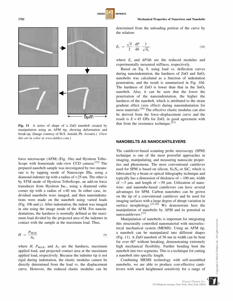
ORDER REPRINTS
faces directly against the gold ball Because of the
difference in the surface work function between the ZnO
nanobelt and the counter Au ball a static charge Q0 exists
at the tip of the nanobelt to balance this potential
difference[31] The magnitude of Q0 is proportional to
the difference between the work function of the nanobelt
tip (NBT) and the Au electrode Q0 = a (fAufNBT)
where a is related to the geometry and distance between
the nanobelt and the electrode
The measurement is based on the mechanical reso-
nance of the nanobelt induced by an externally alternative
electric field Experimentally a constant voltage Vdc and
an oscillating voltage Vaccos2pft are applied onto the
nanobelt (Fig 13a) where f is the frequency and Vac is
the amplitude Thus the total induced charge on the
nanobelt is
Q frac14 Q0 thorn aeethVdc thorn Vac cos 2pftTHORN eth11THORN
The force acting on the nanobelt is proportional to the
square of the total charge on the nanobelt
F frac14 bfrac12Q0 thorn aeethVdc thorn Vac cos 2pftTHORN2
frac14 a2bffrac12ethfAu fNBT thorn eVdcTHORN2 thorn e2V2ac=2
thorn 2eVacethfAu fNBT thorn eVdcTHORN
cos 2pft thorn e2V2ac=2 cos 4pftg
eth12THORN
where b is a proportional constant In Eq 12 the first term
is constant and it causes a static deflection of the ZnO
nanobelt The second term is a linear term and the res-
onance occurs if the applied frequency f is tuned to the
intrinsic mechanical resonance frequency f0 of the ZnO
nanobelt The most important result of Eq 12 is that for
the linear term the resonance amplitude A of the nanobelt
is proportional to Vac(fAufNBT+eVdc)
The principle of the measurement is as follows We
first set Vdc = 0 and tune the frequency f to get the
mechanical resonance induced by the applied oscillat-
ing field Second under the resonance condition of
keeping f = f0 and Vac constant slowly change the mag-
nitude of Vdc from zero to a value Vdc0 that satisfies
fAufNBT+eVdc0 = 0 At this moment the resonance
amplitude A becomes zero although the external ac
voltage is still in effect Therefore the work function at the
tip of the ZnO nanobelt is fNBT = fAu+eVdc0 while
fAu = 51 eV Fig 14 is a plot of the vibration amplitude
A of the nanobelt as a function of the applied direct cur-
rent voltage Vdc from which the value for Vdc0 is
determined The work function of the ZnO nanobelts is
52 eV[32]
CONCLUSION
The property characterization of nanomaterials is chal-
lenged by their small-size structures because of the
difficulties in manipulation A typical example is the me-
chanical properties of individual 1-D nanostructures such
as nanotubes nanowires and nanobelts This chapter
reviews the experimental methods for measuring the
mechanical properties of 1-D nanostructures using a reso-
nance technique in TEM The static and dynamic pro-
perties of the 1-D nanostructures can be obtained by
applying controllable static and alternating electric fields
Fig 14 A plot of vibration amplitude of a ZnO nanobelt as a
function of the applied direct current voltage from which the
offset voltage Vdc0 =012 V
Fig 13 Experimental set-up for measuring the work function
at the tip of a ZnO nanobelt
1784 Mechanical Properties of Nanowires and Nanobelts
ORDER REPRINTS
The resonance of carbon nanotubes can be induced by
tuning the frequency of the applied voltage The technique
is powerful in such a way that it can directly correlate
the atomic-scale microstructure of the carbon nanotube
with its physical properties providing a one-to-one
correspondence in structurendashproperty characterization
Because of the rectangular cross section of the
nanobelt two fundamental resonance modes have been
observed corresponding to two orthogonal transverse
vibration directions showing the versatile applications
of nanobelts as nanocantilevers and nanoresonators The
bending modulus of the ZnO nanobelts was measured to
be 52 GPa Nanobelts have also been demonstrated as
ultrasmall nanocantilevers for sensor and possibly imag-
ing applications in AFM
ACKNOWLEDGMENTS
The results reviewed in this paper were partially contrib-
uted from my group members and collaborators Ruiping
Gao Xuedong Bai Scott Mao William Hughes and Enge
Wang to whom I am very grateful Research supported by
NSF NASA and NSFC
REFERENCES
1 Wang ZL Liu Y Zhang Z Handbook of
Nanophase and Nanostructured Materials 2002
Vols IndashIV Tsinghua University Press Beijing
Kluwer Academic Publisher New York
2 Wang ZL Hui C Electron Microscopy of
Nanotubes Kluwer Academic Publisher New York
2003
3 Poncharal P Wang ZL Ugarte D de Heer
WA Electrostatic deflections and electromechani-
cal resonances of carbon nanotubes Science 1999283 1513ndash1516
4 Wang ZL Poncharal P de Heer WA Nano-
measurements of individual carbon nanotubes by
in-situ TEM Pure Appl Chem 2000 72 209ndash
219
5 Gao RP Wang ZL Bai ZG de Heer WA
Dai LM Gao M Nanomechanics of aligned
carbon nanotube arrays Phys Rev Lett 2000 85622ndash635
6 Wang ZL Poncharal P de Heer WA Measur-
ing physical and mechanical properties of individual
carbon nanotubes by in-situ TEM J Phys Chem
Solids 2000 61 1025ndash1030
7 Meirovich L Elements of Vibration Analysis
McGraw-Hill New York 1986
8 Liu JZ Zheng QS Jiang Q Effect of ripping
mode on resonances of carbon nanotubes Phys Rev
Lett 2001 86 4843ndash4846
9 Wang ZL Dai ZR Bai ZG Gao RP Gole
JL Side-by-side silicon carbide-silica biaxial nano-
wires Synthesis structure and mechanical proper-
ties Appl Phys Lett 2000 77 3349ndash3351
10 Pan ZW Dai ZR Wang ZL Nanobelts of
semiconducting oxides Science 2001 291 1947ndash
1949
11 Wang ZL Pan ZW Dai ZR Semiconducting
Oxide Nanostructures US Patent No 6586095
July 1 2003
12 Dai ZR Pan ZW Wang ZL Gallium oxide
nanoribbons and nanosheets J Phys Chem B
2002 106 902ndash904
13 Dai ZR Pan ZW Wang ZL Growth and
structure evolution of novel tin oxide diskettes J
Am Chem Soc 2002 124 8673ndash8680
14 Kong XY Wang ZL Spontaneous polarization
and helical nanosprings of piezoelectric nanobelts
Nano Lett 2003 in press15 Wen XG Zhang WX Yang SH Dai ZR
Wang ZL Solution phase synthesis of Cu(OH)sub
2nanoribbons by coordination self-assembly using
Cusub 2S nanowires as precursors Nano Lett
2002 2 (12) 1397ndash1401
16 Li YB Bando Y Golberg D Kurashima K
Field emission from MoOsub 3nanobelts Appl
Phys Lett 2002 81 (26) 5048ndash5050
17 Zhou J Xu NS Deng SZ Chen J She JC
Wang ZL Large-area nanowire arrays of molyb-
denum and molybdenum oxides Synthesis and field
emission properties Adv Mater 2003 in press18 Li YB Bando Y Sato T Preparation of
network-like MgO nanobelts on Si substrate Chem
Phys Lett 2002 359 (1ndash2) 141ndash145
19 Liu J Cai J Son YC Gao QM Suib SL
Aindow M Magnesium manganese oxide nano-
ribbons Synthesis characterization and catalytic
application J Phys Chem B 2002 106 (38) 9761
20 Wen XG Zhang WX Yang SH Synthesis of
Cu- (OH)2 and CuO nanoribbon arrays on a copper
surface Langmuir 2003 19 5898ndash5903
21 Bai XD Wang EG Gao PX Wang ZL
Dual-mode mechanical resonance of individual
ZnO nanobelts Appl Phys Lett 2003 824806ndash4808
22 Carlotti G Socino G Petri A Verona E
Acoustic investigation of the elastic properties of
ZnO films Appl Phys Lett 1987 51 1889ndash1891
Mechanical Properties of Nanowires and Nanobelts 1785
M
ORDER REPRINTS
23 Mao SX Zhao MH Wang ZL Probing nano-
scale mechanical properties of individual semicon-
ducting nanobelt Appl Phys Lett 2002 83 993ndash
995
24 Duan DM Wu N Slaughter WS Mao SX
Length scale effect on mechanical behavior due to
strain gradient plasticity Mater Sci Eng A 2001A303 (1ndash2) 241ndash249
25 Yenilmez E Wang Q Chen RJ Wang D
Dai HJ Wafer scale production of carbon
nanotube scanning probe tips for atomic force
microscopy Appl Phys Lett 2002 80 (12)2225ndash2227
26 Dai HJ Hafner JH Rinzler AG Colbert
DT Smalley RE Nanotubes as nanoprobes in
scanning probe microscopy Nature 1996 384147ndash150
27 Hughes W Wang ZL Nanobelt as nanocantile-
ver Appl Phys Lett 2003 82 2886ndash2888
28 Lee CJ Lee TJ Lyu SC Zhang Y Ruh H
Lee HJ Field emission from well-aligned zinc
oxide nanowires grown at low temperature Appl
Phys Lett 2002 81 (19) 3648ndash3650
29 Fowler RH Nordherim LW Electron emission
in intense electric fields Proc R Soc Lond A
1928 119 (781) 173
30 Gao RP Pan ZW Wang ZL Work function at
the tips of multi-walled carbon nanotubes Appl
Phys Lett 2001 78 1757ndash1759
31 Kelvin L Philos Mag 1898 46 82
32 Bai XD Wang EG Gao PX Wang ZL
Measuring the work function at a nanobelt tip and at
a nanoparticle surface Nano Lett 2003 3 1147ndash
1150
1786 Mechanical Properties of Nanowires and Nanobelts
Request PermissionOrder Reprints
Reprints of this article can also be ordered at
httpwwwdekkercomservletproductDOI101081EENN120013387
Request Permission or Order Reprints Instantly
Interested in copying and sharing this article In most cases US Copyright Law requires that you get permission from the articlersquos rightsholder before using copyrighted content
All information and materials found in this article including but not limited to text trademarks patents logos graphics and images (the Materials) are the copyrighted works and other forms of intellectual property of Marcel Dekker Inc or its licensors All rights not expressly granted are reserved
Get permission to lawfully reproduce and distribute the Materials or order reprints quickly and painlessly Simply click on the Request Permission Order Reprints link below and follow the instructions Visit the US Copyright Office for information on Fair Use limitations of US copyright law Please refer to The Association of American Publishersrsquo (AAP) website for guidelines on Fair Use in the Classroom
The Materials are for your personal use only and cannot be reformatted reposted resold or distributed by electronic means or otherwise without permission from Marcel Dekker Inc Marcel Dekker Inc grants you the limited right to display the Materials only on your personal computer or personal wireless device and to copy and download single copies of such Materials provided that any copyright trademark or other notice appearing on such Materials is also retained by displayed copied or downloaded as part of the Materials and is not removed or obscured and provided you do not edit modify alter or enhance the Materials Please refer to our Website User Agreement for more details
ORDER REPRINTS
23 Mao SX Zhao MH Wang ZL Probing nano-
scale mechanical properties of individual semicon-
ducting nanobelt Appl Phys Lett 2002 83 993ndash
995
24 Duan DM Wu N Slaughter WS Mao SX
Length scale effect on mechanical behavior due to
strain gradient plasticity Mater Sci Eng A 2001A303 (1ndash2) 241ndash249
25 Yenilmez E Wang Q Chen RJ Wang D
Dai HJ Wafer scale production of carbon
nanotube scanning probe tips for atomic force
microscopy Appl Phys Lett 2002 80 (12)2225ndash2227
26 Dai HJ Hafner JH Rinzler AG Colbert
DT Smalley RE Nanotubes as nanoprobes in
scanning probe microscopy Nature 1996 384147ndash150
27 Hughes W Wang ZL Nanobelt as nanocantile-
ver Appl Phys Lett 2003 82 2886ndash2888
28 Lee CJ Lee TJ Lyu SC Zhang Y Ruh H
Lee HJ Field emission from well-aligned zinc
oxide nanowires grown at low temperature Appl
Phys Lett 2002 81 (19) 3648ndash3650
29 Fowler RH Nordherim LW Electron emission
in intense electric fields Proc R Soc Lond A
1928 119 (781) 173
30 Gao RP Pan ZW Wang ZL Work function at
the tips of multi-walled carbon nanotubes Appl
Phys Lett 2001 78 1757ndash1759
31 Kelvin L Philos Mag 1898 46 82
32 Bai XD Wang EG Gao PX Wang ZL
Measuring the work function at a nanobelt tip and at
a nanoparticle surface Nano Lett 2003 3 1147ndash
1150
1786 Mechanical Properties of Nanowires and Nanobelts
Request PermissionOrder Reprints
Reprints of this article can also be ordered at
httpwwwdekkercomservletproductDOI101081EENN120013387
Request Permission or Order Reprints Instantly
Interested in copying and sharing this article In most cases US Copyright Law requires that you get permission from the articlersquos rightsholder before using copyrighted content
All information and materials found in this article including but not limited to text trademarks patents logos graphics and images (the Materials) are the copyrighted works and other forms of intellectual property of Marcel Dekker Inc or its licensors All rights not expressly granted are reserved
Get permission to lawfully reproduce and distribute the Materials or order reprints quickly and painlessly Simply click on the Request Permission Order Reprints link below and follow the instructions Visit the US Copyright Office for information on Fair Use limitations of US copyright law Please refer to The Association of American Publishersrsquo (AAP) website for guidelines on Fair Use in the Classroom
The Materials are for your personal use only and cannot be reformatted reposted resold or distributed by electronic means or otherwise without permission from Marcel Dekker Inc Marcel Dekker Inc grants you the limited right to display the Materials only on your personal computer or personal wireless device and to copy and download single copies of such Materials provided that any copyright trademark or other notice appearing on such Materials is also retained by displayed copied or downloaded as part of the Materials and is not removed or obscured and provided you do not edit modify alter or enhance the Materials Please refer to our Website User Agreement for more details