meeting the challenge for offline smps through improved...
TRANSCRIPT
Meeting the challenge for offline SMPS through improved semiconductor current
density
Meeting the challenge for offline SMPS Meeting the challenge for offline SMPS through improved semiconductor current through improved semiconductor current
densitydensity
Jon Mark HancockJon Mark HancockInfineon Technologies NA, Inc.Infineon Technologies NA, Inc.
1730 North First Street1730 North First StreetSan Jose, CA. 95112San Jose, CA. 95112
Page 2
IBM Power & Cooling
Symposium 2005
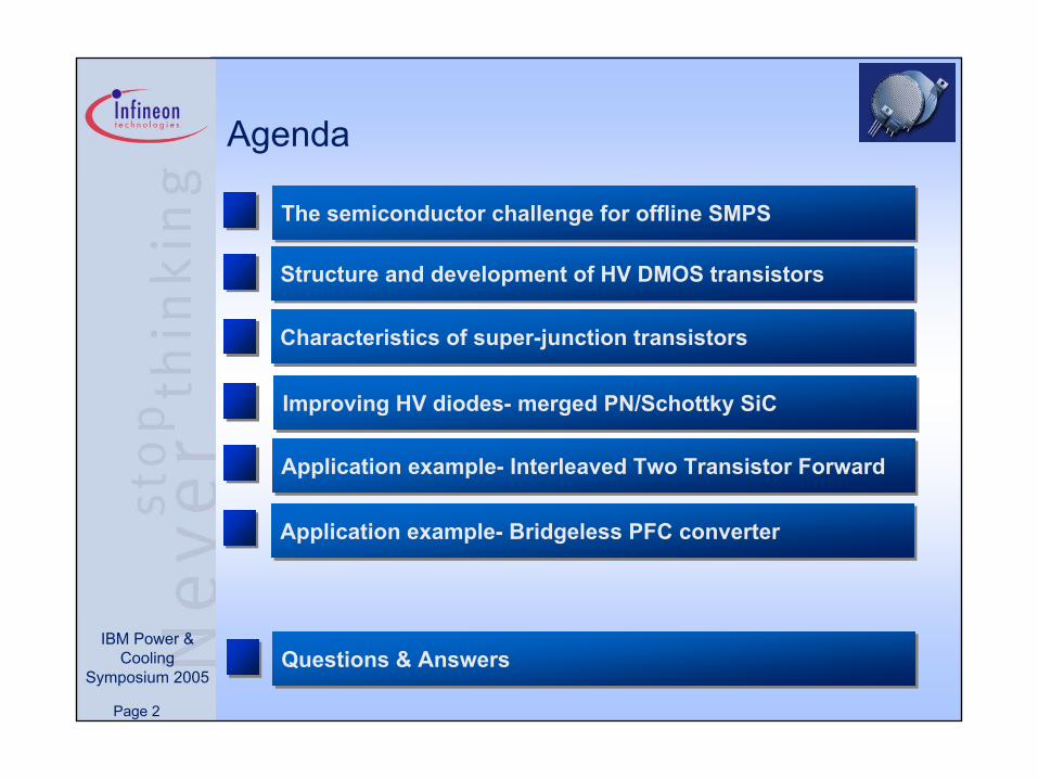
Agenda
The semiconductor challenge for offline SMPSThe semiconductor challenge for offline SMPS
Application example- Interleaved Two Transistor Forward Application example- Interleaved Two Transistor Forward
Structure and development of HV DMOS transistorsStructure and development of HV DMOS transistors
Characteristics of super-junction transistorsCharacteristics of super-junction transistors
Improving HV diodes- merged PN/Schottky SiCImproving HV diodes- merged PN/Schottky SiC
Questions & AnswersQuestions & Answers
Application example- Bridgeless PFC converterApplication example- Bridgeless PFC converter

Page 3
IBM Power & Cooling
Symposium 2005
Requirements for MOSFET’s and Diodes show continuous evolution in expectations
Is the good enough?(considering FOM based on
Ron X Ciss or Coss)
Is the good enough?(considering FOM based on
Ron X Ciss or Coss)
What’s most important?(switching loss improvement, or
surge current at low line?)
What’s most important?(switching loss improvement, or
surge current at low line?)

Page 4
IBM Power & Cooling
Symposium 2005
Near zero power losses
low static power losses• Low on state resistance
• Attractive thermal coefficients
• Low thermal impedance
low dynamic power losses• fast switching speed – ease of drive
• Low energy stored in output capacitance (small area)
• Freedom from charge recombination losses
Lowest possible “Area Specific on state resistance” benefits both major loss mechanisms -
Lower Ron- Smaller chip area –
But it there a downside?
High voltage power switches What should the ideal power switch look like?

Page 5
IBM Power & Cooling
Symposium 2005
Choice of Topologies in often dictated by available power devices and voltage ratings versus Vf
Current FedPush-Pull
com
plex
ity
Phase Shifted Full Bridge
Full Bridge
Half Bridge
Two Transistor Forward
Single Transistor Forward
Resonant Reset Forward
Flyback
Topologies
1 10 100 1000 10000output power, watts
Half Bridge
Dual Interleaved Forward Converter
Server

Page 6
IBM Power & Cooling
Symposium 2005
Characteristics of major SMPS Topologies
HighGood – tap or CD req’dPin/2Vin600 to 5kWZVS Bridge
High2 X F<1Excellent – flexible output configurations
Pin/ Pin/2
Vin X 2, Vin150 to 1kW 600 to 5kW+
CF PP/CF Bridge
High2 X F<1Good – tap or CD req’dPin/2Vin500 to 2kWFull Bridge
Moderate2 X F<1Good- sec tap req’dPin/2Vin50 to 500WHalf Bridge
Moderate2 X F<1Moderate taps req’dPin/22 X Vin+50 to 500WPush-Pull
ModerateF<1N/A (not isolated)PinVin/(1-D) 10 to 100WCuk
High2 X F<0.5Fair-good- no tapsPin/2Vin500 to 2kW+ITTF
ModerateF<0.5Fair-good- no tapsPinVin100 to 800W2T Forward
LowF<0.7ExcellentNo taps required
PinCan be > 2-3X Vin10 to 250WHV 500W+
Resonant Reset Forward
LowF<0.5Fair-goodno taps required
Pin2 X Vin10 to 250W1T Forward
Low-moderateF<0.5Poor/specialized designPinVin+(Np/Ns)*Vout5 to 150WFlyback
Relative Total Cost
Out Ripple Frequency
Duty Cycle
Transformer UtilizationSwitch power
Switch voltage Useful power level
Topology

Page 7
IBM Power & Cooling
Symposium 2005
Where is the main part of RDS[on] in HV MOSFETs? Why is this a problem?
Source Gate
RS*
p+
n-
Drain
Poly-Gate
Repi
RSub
RchRn+Ra
n+
n+SiO2
AL metalization
Drain metalization
substrate
drift regionVDS ≈ 30V
RS* ≈ 7 %Rn+ ≈ 6 %Rch ≈ 28 %Ra ≈ 23 %Repi ≈ 29 %Rsub ≈ 7 %
RDS(on) Analysis
RS* = packaging
RS* ≈ 0.5%Rn+ ≈ 0.5 %Rch ≈ 1.5 %Ra ≈ 0.5 %Repi ≈ 96.5 %Rsub ≈ 0.5 %
VDS ≈ 600V
96.5% of RDS(on) for high voltage standard MOSFET determined by the epitaxial resistance
Conventional epi MOSFETRon /Area ~ V(BR)DSS
2,4...2,6
RDS[ON] is determined by the epitaxial layer-typically 8 mm for 60V MOSFETs,typically 60-70 mm for 600V MOSFETs

Page 8
IBM Power & Cooling
Symposium 2005
Key milestones in planar DMOS Power MOSFET switches development timeline
1st DMOS gen.Lidow, Kinzer
2nd DMOS gen.Chen & Hu, IEEE 1982
SOTA DMOS KobayashiISPSD 2001
Page 9
IBM Power & Cooling
Symposium 2005
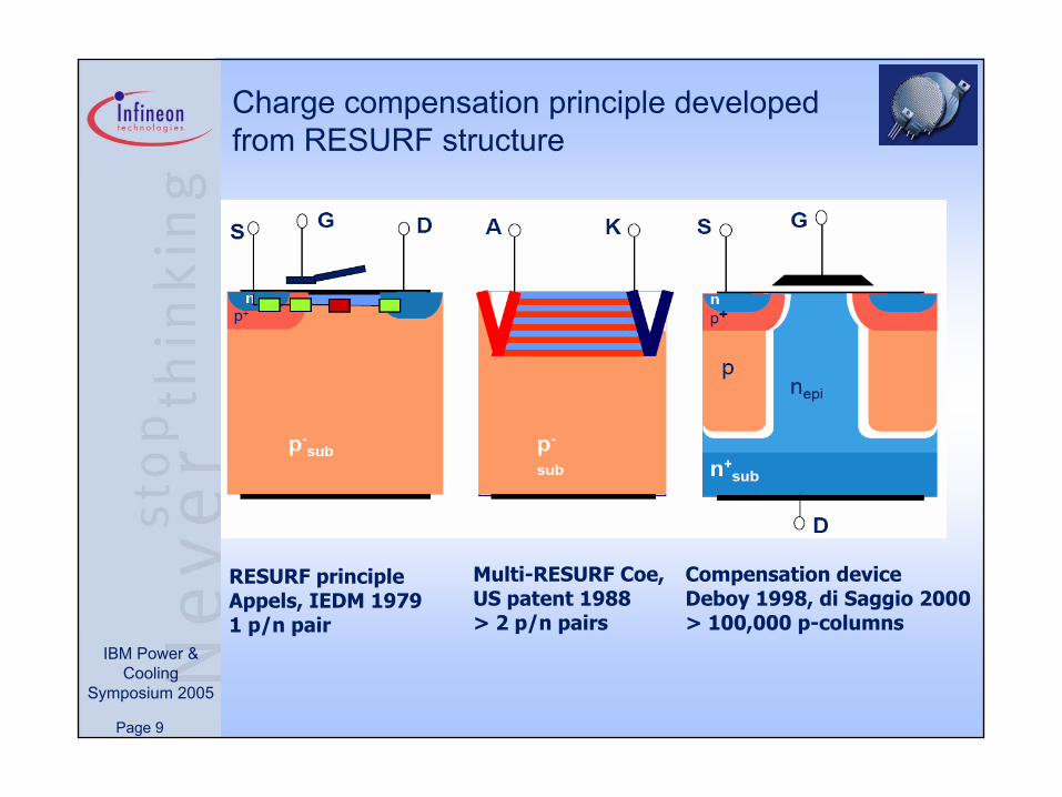
Charge compensation principle developed from RESURF structure
RESURF principleAppels, IEDM 19791 p/n pair
Multi-RESURF Coe, US patent 1988> 2 p/n pairs
Compensation deviceDeboy 1998, di Saggio 2000> 100,000 p-columns

Page 10
IBM Power & Cooling
Symposium 2005
Super Junction MOSFETs use charge compensation principle:
Increasing drain voltage forms folded depletion region
When the transistor is turning off, the thin depletion region at low voltage follows the structure of the P=columns, resulting in high output capacitance at VDS < 35 V
Source Gate
Drain
Poly-Gate
Repi
RSub
Ra
n+
n+SiO2
AlSi metalization
Drain metalization
substrate
p+
current ID
n+
Gate spacer
RS*
n-
Rn+ Rch
Depletion region forms with merging of carriers from doping in n+ region and p+
Charge compensation column structure under p-wells in source

Page 11
IBM Power & Cooling
Symposium 2005
VDS = 0 VVDS = 1 VVDS = 5 VVDS = 10 VVDS = 50 VVDS = 100 VVDS = 250 VVDS = 650 V
Visualization of Voltage Potential gradients during turn-off state animationDevice concept

Page 12
IBM Power & Cooling
Symposium 2005
Loss balance example for hard switching- DMOS vssuperjunction MOSFET
Intrinsic switching losses at hard turn-on
dVVVfPV
swon ⋅⋅= ∫max
0dsCA )()(
There is an optimum chip sizeIn each transistor technology for minimum total power dissipation at a given clock frequency
)A()A( 2onrmsstat RIP ⋅=
Conduction losses

Page 13
IBM Power & Cooling
Symposium 2005
Six years later, Super-junction moves from 14 µm to 7.5 µm cell pitch to lower area specific Ron

Page 14
IBM Power & Cooling
Symposium 2005
Coss as a function of VDS for C3 and C5 generation CoolMOS™ with 380 mΩ on state resistance

Page 15
IBM Power & Cooling
Symposium 2005
Improved area specific Ron leads to lower output capacitance and switching loss
P-column form large folded capacitor at low voltage
Smaller cell pitch needed to increase doping levels in current path and charge compensation structure
High capacitance at low voltage increases energy storage, but also acts as non-linear turn-off snubber
Capacitance falls to very low levels at high voltage (over 100V), contributing to low turn-on switching loss

Page 16
IBM Power & Cooling
Symposium 2005
Non-linear output capacitance acts as dynamicsnubber with low output Ceff reduces losses
Switching energy will be stored in the output capacitance and not dissipated in the channel during turn-off transient
Switching energy will be stored in the output capacitance and not dissipated in the channel during turn-off transient
10
100
1000
10000
0 50 100 150 200 300
Cap
acita
nce
[pF]
Cgd
Compensation MOSStandard-MOS
Vds [V]
600V / 190 mΩ
Cgs
Cds

Page 17
IBM Power & Cooling
Symposium 2005
New Merged Schottky-PN Structure –with Low Ohmic connection P Regions
SiC – wide bandgap material- typical room temp PN junction potential of 3 V
P regions not only reduce voltage gradient at Schottky barrier, but are terminated with low ohmic connection
Above junction potential, PN junctions provide PN diode operation
-10
-8
-6
-4
-2
0
2
4
6
8
10
0.07 0.1 0.13 0.16 0.19 0.22 0.25Time [µs]
I [A
]
thinQ! SiC Schottky diodeSi pn tandem diodeultrafast Si pn diode
T=150°C, VDC=400V

Page 18
IBM Power & Cooling
Symposium 2005
Forward characteristic with 400µs pulse time at temperatures from -55°C to 175°C
Bipolar behavior verified
100% testing of Vf at 6X rated current

Page 19
IBM Power & Cooling
Symposium 2005
Comparing Surge and i2t Capability with standard SiC diode
3X Greater IFSM
6X Greater i2t value

Page 20
IBM Power & Cooling
Symposium 2005
2nd Gen SiC Schottky diode - stable avalanche with positive temperature coefficient

Page 21
IBM Power & Cooling
Symposium 2005
Interleaved two transistor Forward Converter and primary switch waveforms, secondary current waveforms
Current ripple cancellation eases output capacitor
requirements

Page 22
IBM Power & Cooling
Symposium 2005
The ITTF has interesting characteristics for isolated supply stage
Basic characteristics
Simple, highly efficient topologyOutput stage and voltage ripple identical to ZVS with current doublerEasy current control schemeNo resonance inductorEspecially highly efficient at low load, good for redundant PSNo use of body diode, better potential MOSFET reliabilityTTF topology well known from lower power rangesSnubbing optimization and other “tweaks” indicate further gains are possibleLess complex system design = shorter time to market

Page 23
IBM Power & Cooling
Symposium 2005
Selection criteria based on Operating conditions – Forward PWM Isolation stage
Two Transistor Forward, ITTF Converter Characterisitc– Input voltage range 300V DC to 400VDC typical- typical 25 – 35% range of I2 x R– No body diode conduction– Selection based on FOM and balance of conduction losses (I2 x R) and switching
losses (Ceff X Fclk plus crossover losses)
Main selection criteria:– VDS[BR] rating– R[DS]on
– Couteffective Energy Related– Switching Crossover losses
Secondary selection criteria- Gate charge, R Gate, and ID ratingsSuggest FOM based on RDS[on] X Couteffective Energy relatedOptimum component selection based on balancing conduction losses and fixed switching losses over load range, light to full load; applications envelope doesn’t have wide worst case range

Page 24
IBM Power & Cooling
Symposium 2005
Application Evaluation:RDS[on], CO[effective], Gate Qg total

Page 25
IBM Power & Cooling
Symposium 2005
Example- 1 kW ITTF @ 130 kHz – 400V busWorst case Loss component estimation for IPP60R99CS
Same calculations for IPP60R199CP transistor:• Same crossover loss, • Coss related loss is cut in half to ~3/4 watt, • conduction loss only rises to ½ watt • total losses drop from 3.9 watts to 3.3 watt, • Costs are reduced with much smaller chip in the forward transistor. • Net gain is about 2.4 watts of less dissipation, notching the overall efficiency up about 0.24%.
( )2
_ [ ] ( ) 0.252 WattConduction Peak Sw DS on JPd I R T= × =Estimated conduction losses at peak switching current
__
_ min max
3.672
Out MaxPEAK Sw
In
PI A
V D
= = × ×
Peak Switching Current under bulk bus low line (300V)
( )_ max_ 2.028 Watt
2In
Switching Peak Sw on off S
VPd I t t f
= × × + × =
Estimated Crossover Switching losses (tends to be over-estimated for CoolMOS)
2( ) _
1 1.526 Watt2Coss O ER In Max SPd C V f= × × × =Estimated switching loss from
COSS (using CO(ER) )
0.1 Wattgate G Gate SPd Q V f= × × =Estimated gate drive loss:

Page 26
IBM Power & Cooling
Symposium 2005
0,75
0,8
0,85
0,9
0,95
200 400 600 800 1000P in [W]
Effic
ienc
y
ZVS CoolMOS™ CS
ITTF CoolMOS™ CS
ITTF Competitor
The ITTF shows efficiency gain at light load … especially in the range common with redundant shared supplies
7 % points better efficiency at 1/3 load
1 % better over next best alternative at full load

Page 27
IBM Power & Cooling
Symposium 2005
High Efficiency PFC-Stage eliminates bridge rectifier
Concept In development
Mai
n co
nver
ter i
nclu
ding
with
isol
atio
n
AC
D1 D2
L1
L2
C1
Bulk
Q1 Q2D3 D4
ID2ID1
IQ1 IQ2
ID1ID2
PFC Choke
VACIN

Page 28
IBM Power & Cooling
Symposium 2005
First Prototype Power Stage Configuration

Page 29
IBM Power & Cooling
Symposium 2005
Control Implementation with ICE1PCS01

Page 30
IBM Power & Cooling
Symposium 2005
99% efficiency PFC stage demoboard
Semiconductors:
CoolMOSTM CS (99mOhm)
600V thinQ!TM 2nd Gen. SiC diode
ICE1PCS01 as Control IC
Output power: 1500WInput Voltage: 207…264 VOutput Voltage: 380 Vfsw= 130 kHz

Page 31
IBM Power & Cooling
Symposium 2005
Nearly 99% efficiency at 1500W output
96,5
97,0
97,5
98,0
98,5
99,0
99,5
100,0
0 300 600 900 1200 1500Pout [W]
Effic
ienc
y [%
]
Competitor, 4*500V/0.25Ohm
CoolMOS CS,2*IPP60R099CS
Efficiency: 98.9 % @ 230 V input @ full load

Page 32
IBM Power & Cooling
Symposium 2005
References
Brian Griffith, “High Density AC/DC Power Supplies”, Intel Technology Symposium, 2002
G. Deboy,M. März, J. Stengl, H. Strack, J. Tihanyi, H. Wever, “A new generation of high voltage MOSFETs breaks the limit of silicon”, pp. 26.2.1-26.2.3, Proc. IEDM 98, San Francisco, Dec. 1998.
M. Saggio, D. Fagone, S. Musumeci, “MDmesh™: innovative technology for high voltage power MOSFETs”, Proc. ISPSD 200, pp. 65-68, Toulouse May 2000.
B. Lu, W. Dong, Q. Zhao, F. Lee, "Performance Evaluation of CoolMOS and SiC Diode for Single-Phase Power Factor Correction Applications", APEC 2003 Conference proceedings.
L. Hriscu, G. Casaru, “Low Loss Snubbing in DC-DC Converters”, Proc. Electronica Power Electronics Conference April 2004, San Francisco.