meeting the shielding challenges of injection-molded … · plastic part. electroless plating ......
TRANSCRIPT
3� Conformity DeCember 2008
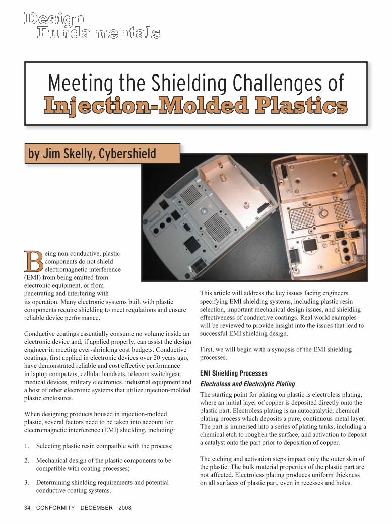
Being non-conductive, plastic components do not shield electromagnetic interference
(EMI) from being emitted from electronic equipment, or from penetrating and interfering with its operation. Many electronic systems built with plastic components require shielding to meet regulations and ensure reliable device performance.
Conductive coatings essentially consume no volume inside an electronic device and, if applied properly, can assist the design engineer in meeting ever-shrinking cost budgets. Conductive coatings, first applied in electronic devices over 20 years ago, have demonstrated reliable and cost effective performance in laptop computers, cellular handsets, telecom switchgear, medical devices, military electronics, industrial equipment and a host of other electronic systems that utilize injection-molded plastic enclosures.
When designing products housed in injection-molded plastic, several factors need to be taken into account for electromagnetic interference (EMI) shielding, including:
Selecting plastic resin compatible with the process;
Mechanical design of the plastic components to be compatible with coating processes;
Determining shielding requirements and potential conductive coating systems.
1.
2.
3.
This article will address the key issues facing engineers specifying EMI shielding systems, including plastic resin selection, important mechanical design issues, and shielding effectiveness of conductive coatings. Real world examples will be reviewed to provide insight into the issues that lead to successful EMI shielding design.
First, we will begin with a synopsis of the EMI shielding processes.
EMI Shielding Processes
Electroless and Electrolytic Plating
The starting point for plating on plastic is electroless plating, where an initial layer of copper is deposited directly onto the plastic part. Electroless plating is an autocatalytic, chemical plating process which deposits a pure, continuous metal layer. The part is immersed into a series of plating tanks, including a chemical etch to roughen the surface, and activation to deposit a catalyst onto the part prior to deposition of copper.
The etching and activation steps impact only the outer skin of the plastic. The bulk material properties of the plastic part are not affected. Electroless plating produces uniform thickness on all surfaces of plastic part, even in recesses and holes.
Meeting the Shielding Challenges of Injection-Molded Plastics
by Jim Skelly, Cybershield

DeCember 2008 Conformity 35
Once the electroless copper layer is deposited onto the plastic part, additional copper thickness can be deposited as required for EMI shielding performance, and/or can be finished with nickel, tin or gold to provide the functional metal coating to meet the full range of mechanical, electrical, environmental and appearance requirements. Typically, electroless plating is used to deposit thin metal coatings, from 0.00004” (1.0 µm) to 0.0005” (12.5 µm).
If thicker coatings are required, electrolytic plating (also called electroplating) can be used to deposit thicker coatings of copper, nickel, tin, chrome, silver, and gold over the electroless copper plated part. Electroplating deposits at faster rates and lower costs compared to the same thickness of electroless plating; however, electroplating is a line-of-sight process that will yield wider thickness variation over a part than does electroless plating. Electroplating process can be used to deposit from 0.0002” (5.0 µm) to 0.003” (75 µm) or more metal thickness. Also, electroplating is used to produce decoratively plated plastic parts with available finishes, including nickel, bright and matte chrome, gold, copper and brass, to name a few.
Selecting a plateable resin is among the most critical factors for a successful EMI shielding application. Table 1 lists common injection molded thermoplastic resins. It includes plateable as well as non-plateable resins, and some resin families that include both plateable and non-plateable grades.
Some (but not all) non-plateable resins can be made plateable by custom blending a plating additive into the base resin. Examples of custom blending to produce plateable resins include polypropylene and polyphthalamide. Both resins are typically not plateable but, when custom blended with the plating additive, become plateable.
Plating can be applied over the entire part as described above, or selectively, onto specified areas.
There are several options for selective plating, depending on the required precision for the plating pattern, design, and the plastic resin, as noted below.
Autocatalytic Plating Catalyst
Spray plating catalyst onto the areas of the plastic part, using custom built paint masks to control the location of the catalyst.
The chemical make-up of the catalyst draws copper metal out of the plating solution, and deposits copper uniformly onto the catalyzed area. Following electroless copper plating, electroless nickel plating can be applied to protect the copper from corrosion and abrasion.
The plating catalyst thickness is approximately 0.001” (0.025 mm), and the electroless plating thickness is limited to 0.0001” (2.5 µm) to 0.00025” (6.25 µm). The plastic parts are never exposed to aggressive chemistries; therefore, the molded-in-color and texture of the plastic part are maintained through the process.
Custom Shields & Precision Metal Parts
Shield Design Options:
Board-level
Removable lid
Multi-cavity
Complex geometry
Shielding Materials:
Brass
Steel
Aluminum
Titanium
Nickel Silver
Fotofab works with hundreds of alloys
Prototype or production, think of Fotofab for your shielding needs.
RF Shields & More…Whether you need a multi-cavity shield or a simple five-sided box, Fotofab has a solution for you. Visit our Shielding Design Guide at www.fotofab.com/RF. Have a shield or metal part ready for quote? Submit your specifications and drawing online. Of course, you can always call one of our Technical Sales Staff at (773) 463-6211 to discuss shielding material, plating, design options and cost saving ideas.
Precision Metal PartsWe work with hundreds of alloys ranging from 0.0002” (0.05mm) to 0.090” (2.29mm) thick. Fotofab offers chemically etched parts, laser cutting, plating, electro polishing, tape & reel packaging and more.
Fast DeliveryFotofab understands the importance of a deadline. Our standard lead-time starts at 2 weeks with multiple expedite options available. You can even go from print-to-part as fast as same day! Ask about our 24-hour expedite service!
For over 40 years, Fotofab has been manufacturing quality shields and precision metal parts.
Would you like a copy of our “Design Guide to Photochemical Machining”? Visit us at www.fotofab.com/RF and we will send you a FREE copy.
Innovative solutions - exceptional capabilities
3758 Belmont Avenue Chicago, IL 60618 USAphone 773-463-6211 fax 773-463-3387www.fotofab.com/RF [email protected]

3� Conformity DeCember 2008
Figure 1 shows selectively copper and nickel-plated enclosures for an EMI shielding application.
Plating 2-Shot Molded Components
Mold 2-shot plastic part, with one shot being a plateable resin and the other shot being a non-plateable resin. The plateable resin in the 2-shot molded part is typically catalyzed to include plating additive to promote the electroless copper plating deposition. The mold tool must be specially designed for the 2-shot molding process, and the both plastic resins must have compatible molding parameters.
Peelable Plating Resist
Peelable plating resist can be used to mask defined areas of a part and produce complex masking patterns that are not feasible or cost-effective with alternative processes.
The plating resist is applied onto the required areas by dispensing or spraying, followed by UV cure. The part is subject to conventional electroless plating to apply initial copper plating. The resist is then peeled off the part. Subsequent electroless or electroplating can be used to finish the part to the final requirements.
Table 2 summarizes each selective plating system.
Conductive Paint
Conductive paints are comprised of micron-sized metal particles of nickel, copper, silver plated copper or silver blended into water or a solvent-based paint system. Similar to selective plating process, a masking fixture is used to control the location of the conductive paint that is sprayed onto the required areas of the part. The fully cured conductive paint thickness ranges from 0.0005” (0.0125 mm) to 0.002” (0.05 mm), depending on the paint type and EMI shielding requirement.
The paint can be applied in a manual paint booth, where an operator applies the paint with a paint gun, or with a paint
Common Plateable Resins
Acrylonitrile Butadiene Styrene (ABS)
Polycarbonate (PC)
PC/ABS Polyether Imide (PEI)
Selected or Custom Blended Plateable Grades
Polyphenylene Oxide (PPO)
Epoxy Graphite PC/Polyester
Polypropylene PEEK PPS Liquid Crystal Polymer
Polystyrene Urethane Nylon Polyphthalamide (PPA)
Not Plateable
Polyvinyl Chloride (PVC)
Polyethylene Polybutylene Terephthalate (PBT)
Table 1: Common plateable resins
Figure 1: Selectively copper and nickel-plated enclosures for EMI shielding
Process Candidate Resins Plating Options Plating Precision Comments
Plating Catalyst Primarily ABS and PC/ABS and selected PC resins
Electroless plating only, typically copper/nickel
Plating tolerance of +/-0.025”
Plating interior surfaces of enclosures for EMI shielding or grounding surface.
2-shot Molding Catalyzed resin for plateable area. Non-plateable resin needs to be compatible in molding process to plateable resin
Electroless followed by Electroplating if required. Available metals include copper, nickel, tin, gold and chrome
Tolerance function of 2-shot molding capability. Can attain line width of <0.020” (0.5 mm)
Applications include connectors antennas, IC packaging and sensors
Peelable Plating Resist Plateable resins, including ABS, PC/ABS, Polycarbonate, PEI, PPO, LCP, PPA, etc.
Electroless followed by Electroplating if required. Available metals include copper, nickel, tin, gold and chrome
Subject to part design Suitable for complex part design where 2-shot or laser activation process is not feasible
Table 2: Selective plating processes

DeCember 2008 Conformity 37
robot. The paint robot offers advantages over manual spray methods, especially in higher volume applications where cost is critical. In the robot, the spray pattern can be programmed and frozen to apply the optimal amount of conductive paint across the entire shielded surface. Manual paint application typically has lower set-up cost than robotic painting, and is a good match with lower volume applications.
Table 3 summarizes compatible resins with conductive paint. Difficult to paint resins will usually require primer or other surface preparation prior to the conductive paint process.
Part Design Considerations
As with resin selection, plastic part design is critical to successful application. There are design approaches that should be avoided if possible, as noted in Table 4.
Secondary Processes
Inserts can be molded into the part or installed by heat staking or ultrasonic insertion prior to or after plating. If specifying <100 micro-inches (2.5 µm) electroless plating thickness, inserts can be installed before or after plating. If plating thickness is >100 micro-inches (2.5 µm), or if applying conductive paint, inserts should be installed prior to coating process, and masked during the plating operation with a plug or screw to prevent coating being deposited onto the threads. Brass inserts are compatible with plating processes and conductive paint.
Gaskets for environmental or EMI/RFI seal are installed after plating or painting. Form-in-place gaskets, comprised of silicone with metal particle filler, can be dispensed around perimeter of compartments of plastic part (or metal part) to prevent interference within the device, and/or around the perimeter of the enclosure to provide an EMI seal from the external environment.
The metal particles in the form-in-place gasket material are silver-plated copper, silver-plated nickel or silver-plated aluminum. To minimize risk of galvanic corrosion between
the coating and the gasket, it is recommended to match the form-in-place metal with the coating, that is, use copper-based form-in-place gasket material on copper painted applications, and nickel where the form-in-place gasket is being dispensed onto nickel plated or silver painted parts.
Form-in-place gaskets range in size from 0.016” (0.4 mm) height to 0.100” (2.5 mm), although it is recommended that gasket height be limited to 0.040” (1.0 mm). Form-in-place gaskets have shore hardness of 40-60 and are designed for approximately 50% compression in the assembled application. They can be dispensed into grooves or onto flat rails and surfaces.
Specifying the coating system includes the following elements:
Thickness is usually defined as a minimum. If required, due to part function or fit, plating can be specified as a thickness range.
•
Common Paintable Resins
Acrylonitrile Butadiene Styrene (ABS)
Polycarbonate (PC) PC/ABS Blend
PC/PBT (Xenoy) Poly Aryl Amide Polyphenylene Oxide (PPO)
Polyphthalamide (PPA)
Nylon Polyether Imide (PEI)
Polybutylene Terephthalate (PBT)
Polystyrene (PS) Polyphthalamide (PPA)
Difficult to Paint Resins (May Require Primer)
Polypropylene Polyethylene Liquid Crystal Polymer
Polyimide Teflon (PTFE) PEEK
Table 3: Common paintable resins
Plating Design Issues
Design Don’t Design Alternative
5-sided box or cup design that can trap air and/or drag out plating chemicals, impacting plating quality and cost
Include drain holes, or design part to prevent entrapment of air or plating solution.
Tight crevices that can trap plating solution Eliminate crevices in the design or include drain hole
Small blind holes can trap plating solution that can later weep out and damage the plating.
Utilize through-holes if possible. If blind holes are required, they can be plugged to prevent plating solution entrapment.
Painting Design Issues
Design Don’t Design Alternative
Difficult to paint tight bosses, crevices and holes due to line-of-sight process to apply paint
Eliminate crevices and small holes that require coating
Table 4: Part design considerations

38 Conformity DeCember 2008
The coating resistance can be specified, either in ohms per square or point-to-point ohms resistance. In this case, plating or paint thickness need not be specified.
Coating adhesion is commonly measured according to the ASTM D3359 standard. This standard is based on tape test and a 1-5 scale for the amount of coating removed during the tape test (5 is no metal removed, and 1 is complete removal of the plating).
Cost Trade-offs of Alternative EMI Shielding System
The recurring unit cost and upfront non-recurring expense (NRE) for tooling and fixturing for the different EMI shielding systems are highly dependent on part design, size and complexity. If plating all surfaces of a part is feasible, that will have the lowest unit cost and NRE. Selective plating and conductive paint costs can vary based on complexity of the part design and pattern for the coating.
Table 5 outlines basic cost considerations for each option but, to obtain an accurate cost for the EMI shielding application, the requirements must be analyzed, and the processing details, production cost and tooling/fixturing cost need to be defined for the specific part. Also, as is the case in most industries, unit volumes have sizable impact on unit cost.
•
•
Shielding Requirements and Shielding Effectiveness
Designing for EMI shielding is best done up front, early in the product design cycle. Designing the electronics, the plastic enclosure and EMI shielding system simultaneously as opposed to sequentially can reduce the time-to-market as well as production cost.
The basic EMI shielding principal, also known as the Faraday Cage Principal, is well understood; however, applying the principal to electronic equipment design can present challenges to engineers. Ultimately, compliance to regulations as well as performance in the end use environment needs to be confirmed with fully assembled systems being subjected to EMI testing in a lab.
A few guidelines for EMI shielding coatings can assist the engineer in specifying a coating that will meet the requirements. EMI can be divided into two broad categories, magnetic and electric. Magnetic interference is generally viewed as less than 30 MHz frequency, while electric interference is 30 MHz and above. To shield longer wavelength magnetic interference, thicker coatings that include magnetic materials such as nickel are preferred.
For electric interference, thin conductive coatings comprised of copper or silver typically perform best. In many cases, the conductive metal thickness can be as thin as 1 micron for applications with frequency >30 MHz.
All-Over Plating Autocatalytic Selective Plating
2-Shot Molding Peelable Plating Resist Conductive Paints
Generally lowest unit cost and NRE option
Moderate unit cost and NRE due to 2-step process (coat with catalyst and plate)
Highest NRE due to mold tool complexity to mold 2-shot part design. Plating cost low (similar to all-over plating)
Cost to apply & remove resist can be high depending on masking complexity. Plating cost low (similar to all-over plating)
Moderate unit cost and NRE. 1-step process to apply paint. Paint material cost can be high, which can make parts with large surface area costly.
Table 5: Cost considerations for various shielding options
Attenuation (dB)
Coating System
Thickness (ohms/square) Resistivity
30 MHZ 100 MHz 300 MHz 1 GHz 5 GHz 10 GHz
All-Over Plating
40-400 µ” (1.0-10.0 µm)
5-50 90 108 104 120 113 87
Selective Plating
80-200 µ” (2.0-5.0 µm)
25-100 77 73 71 71 60 63
Copper Paint 0.001-.0015” (0.025-.375 mm)
25-100 65 63 59 70 81 63
Copper-Silver Paint
0.0008-.001” (0.020-.25 mm)
15-50 78 73 72 69 85 82
Silver Paint 0.0005-.001” (0.0125-.025 mm)
15-50 70 71 70 62 70 70
Table 6: EMI shielding effectiveness of conductive coatings

DeCember 2008 Conformity 39
Table 6 displays the surface resistivity and shielding effectiveness of several conductive coating systems, 30 MHz to 10 GHz. It shows that plating onto all surfaces provides the best shielding effectiveness over the frequency range.
Plating on Plastics Applications
Shielded Connectors
Connector designs in today’s electronic equipment face the competing demand for a smaller form factor, lighter weight, improved mechanical performance, increasing need for EMI shielding, and lower cost. Metal shells used to shield connectors add weight, cost and space. Plated plastic connectors are being used to meet the EMI/RFI shielding requirements, thereby reducing weight and space requirements. Nickel thickness can be varied between 50 and 600 micro-inches (1.25-15.0 µm) to meet mechanical and environmental requirements.
Medical Electronic Devices
Shielding medical electronic devices present significant design challenges due to the pervasiveness of electronic equipment in the hospital. Autocatalytic selective plating and conductive paint are applied onto many medical electronic device enclosures to provide EMI shielding.
Military Electronic Equipment
The modern day battlefield is noisy, and military electronic systems need to be shielded against EMI/RFI noise. The move to rapid force deployment drives the need for lightweight mobile electronic systems, and the use of plastics has made significant inroads into the electronic battlefield.
Since plastics do not shield against EMI/RFI, they are usually shielded, often with thick electroplated coatings to protect against the wide EMI/RFI frequency range that may be encountered in the field. The plated plastic components can then be coated with mil-spec finishes, including latest generation water borne chemical agent resistant coating (CARC) paints
Summary
Designing for EMI shielding is best accomplished early in the design cycle before such key issues as plastic resin selection and final part design are finalized. Shielding systems can be tailored to meet the needs of highly cost competitive consumer electronic devices and automotive hardware, as well as critical performance applications in medical devices and military electronics.
Jim Skelly is president of Cybershield, and can be reached at [email protected].
Figure 2: Examples of plated plastic connectors
Figure 3: A example of a typical medical device housing
Figure 4: Some examples of military electronic equipment (photo courtesy of DRS Tactical Systems)
FAST Link www.conformity.com/2460