memory - computer engineeringxyi/coen210/notes/7__memory.pdf · 1 memory dr. bill yi santa clara...
TRANSCRIPT

1
MEMORYMEMORYDr. Bill Yi
Santa Clara University
(Based on text: David A. Patterson & John L. Hennessy, Computer Organization and Design: The Hardware/Software Interface, 3rd Ed., Morgan Kaufmann, 2007)
(Also based on presentation: Dr. Nam Ling, COEN210 Lecture Notes)

2
COURSE CONTENTSCOURSE CONTENTSIntroductionInstructionsComputer ArithmeticPerformanceProcessor: DatapthProcessor: ControlPipelining TechniquesMemoryMemoryInput/Output Devices

3
MEMORYMEMORY
Memory HierarchyCache: Basics, MappingCache: Performance, AssociativityMemory Technology & InterleavingMultilevel CachesVirtual Memory: Basics, Page Tables & TLBSIntegrating Virtual Memory, TLBs, Caches
4
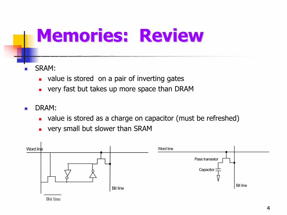
SRAM:value is stored on a pair of inverting gatesvery fast but takes up more space than DRAM
DRAM:value is stored as a charge on capacitor (must be refreshed)very small but slower than SRAM
Memories: ReviewMemories: Review
Word line
Pass transistor
Capacitor
Bit line
Word line
Bit line
Bit line
5
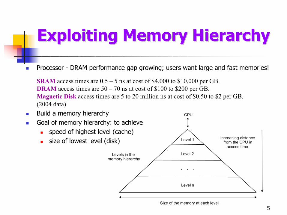
Processor - DRAM performance gap growing; users want large and fast memories!
SRAM access times are 0.5 – 5 ns at cost of $4,000 to $10,000 per GB.DRAM access times are 50 – 70 ns at cost of $100 to $200 per GB.Magnetic Disk access times are 5 to 20 million ns at cost of $0.50 to $2 per GB.(2004 data)Build a memory hierarchyGoal of memory hierarchy: to achieve
speed of highest level (cache)size of lowest level (disk)
Exploiting Memory HierarchyExploiting Memory Hierarchy
CPU
Level n
Level 2
Level 1
Levels in thememory hierarchy
Increasing distancefrom the CPU in
access time
Size of the memory at each level
6
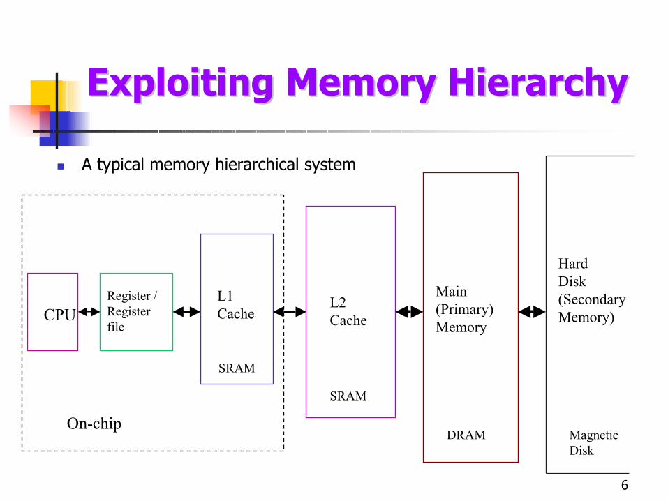
A typical memory hierarchical system
CPURegister / Register file
L1Cache
On-chip
L2Cache
SRAM
SRAM
Main(Primary)Memory
DRAM
HardDisk(SecondaryMemory)
MagneticDisk
Exploiting Memory HierarchyExploiting Memory Hierarchy

7
LocalityLocality
A principle that makes having a memory hierarchy a good idea
If an item is referenced,temporal locality:temporal locality: it will tend to be referenced again soonspatial locality:spatial locality: nearby items will tend to be referenced soon.
Memory hierarchy:keep recently accessed data closer to processor --- temporalmove blocks consisting of contiguous words to upper level --- spatial
Why does code have locality?
Our initial focus: two levels (upper, lower)block: minimum unit of data to transfer between memory levels hit: data requested is in the upper levelmiss: data requested is not in the upper levelHit rate = #hit/#accessMiss rate = 1 - hit rateMiss penalty: time (transfer the block to upper level) + time (delivery data to processor)
8
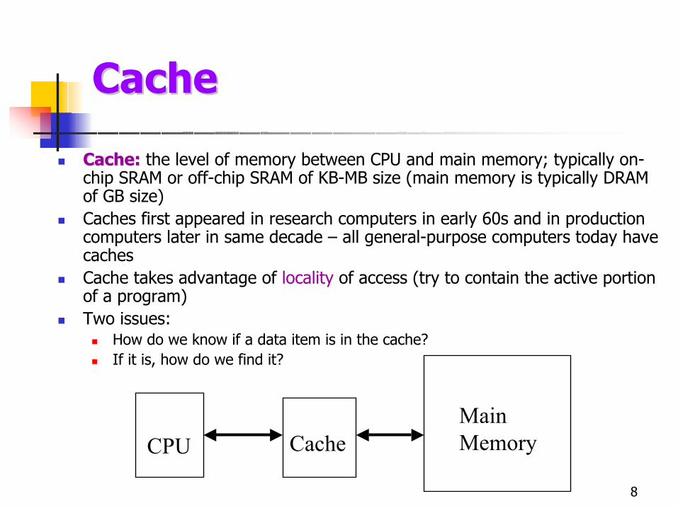
Cache:Cache: the level of memory between CPU and main memory; typically on-chip SRAM or off-chip SRAM of KB-MB size (main memory is typically DRAM of GB size)Caches first appeared in research computers in early 60s and in production computers later in same decade – all general-purpose computers today have cachesCache takes advantage of locality of access (try to contain the active portion of a program)Two issues:
How do we know if a data item is in the cache?If it is, how do we find it?
CacheCache
CPU CacheMainMemory

9
Our first example: block size is one word of dataDirect Mapping: (Block address) modulo (Number of blocks in cache)
Ex. Block 21 maps to Cache block 21 Mod 8 = Cache block 5
Direct Mapped CacheDirect Mapped Cache
00001 00101 01001 01101 10001 10101 11001 11101
000
Cache
Memory
001
010
011
100
101
110
111
For each item of data at the lower level, there is exactly one location in the cache where it might be.e.g. lots of items at the lower level share locations in the upper level

10
IndexIndex: (Block address) modulo (Number of blocks in cache), used to select a block in the cacheTagTag: upper portion of address (bits that are not used as index into the cache), to identify if the block in the cache contains requested word; a comparator can be used to matchValid bitValid bit: to indicate whether an entry contains a valid address (e.g. when CPU starts up, tag bits meaningless)Block offsetBlock offset: to identify word within selected blockByte offsetByte offset: to identify byte within selected word
Recently accessed word in cache → temporal localityWhen a miss occurs, we fetch a block of contiguous words from memory to cache →spatial locality
Basically, when a miss occurs, we stall the CPU, freeze the content of registers; a separate controller handles cache miss, fetches data/instructions from main memory to cache
Direct Mapping: AddressingDirect Mapping: Addressing

11
Accessing a word in a 64KB cache, with 4 words per blockAddress (showing bit positions)
16 12 Byteoffset
V Tag Data
Hit Data
16 32
4Kentries
16 bits 128 bits
Mux
32 32 32
2
32
Block offsetIndexTag
31 16 15 4 3 2 1 0
Direct Mapping: AddressingDirect Mapping: Addressing
12
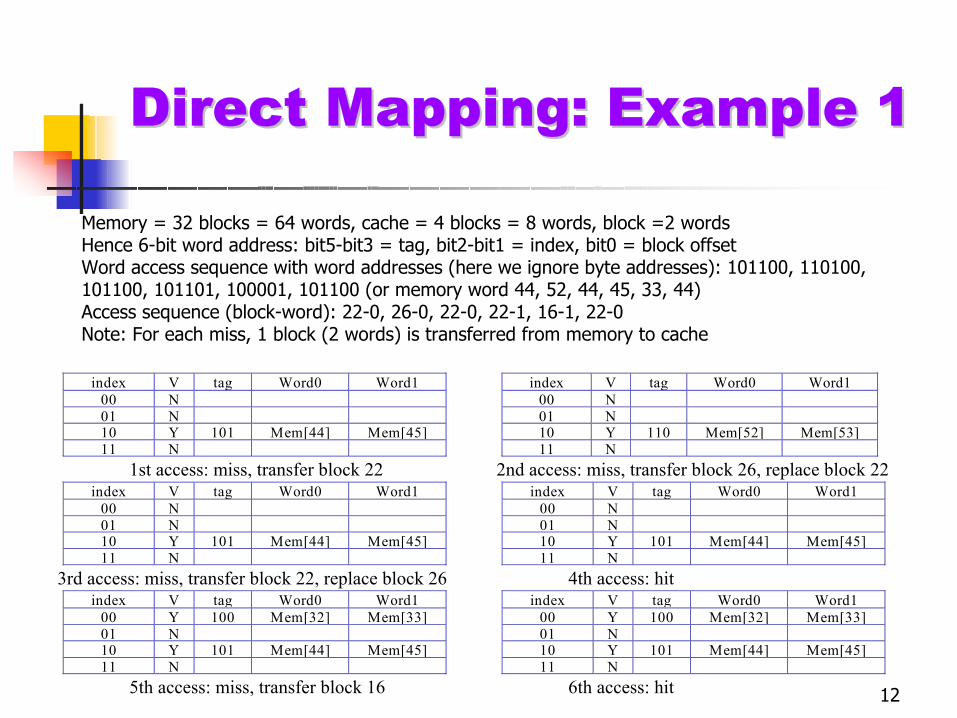
Memory = 32 blocks = 64 words, cache = 4 blocks = 8 words, block =2 wordsHence 6-bit word address: bit5-bit3 = tag, bit2-bit1 = index, bit0 = block offsetWord access sequence with word addresses (here we ignore byte addresses): 101100, 110100, 101100, 101101, 100001, 101100 (or memory word 44, 52, 44, 45, 33, 44)Access sequence (block-word): 22-0, 26-0, 22-0, 22-1, 16-1, 22-0Note: For each miss, 1 block (2 words) is transferred from memory to cache
index V tag Word0 Word100 N01 N10 Y 101 Mem[44] Mem[45]11 N
index V tag Word0 Word100 N01 N10 Y 110 Mem[52] Mem[53]11 N
index V tag Word0 Word100 N01 N10 Y 101 Mem[44] Mem[45]11 N
index V tag Word0 Word100 N01 N10 Y 101 Mem[44] Mem[45]11 N
index V tag Word0 Word100 Y 100 Mem[32] Mem[33]01 N10 Y 101 Mem[44] Mem[45]11 N
index V tag Word0 Word100 Y 100 Mem[32] Mem[33]01 N10 Y 101 Mem[44] Mem[45]11 N
2nd access: miss, transfer block 26, replace block 22
3rd access: miss, transfer block 22, replace block 26 4th access: hit
5th access: miss, transfer block 16 6th access: hit
1st access: miss, transfer block 22
Direct Mapping: Example 1Direct Mapping: Example 1

13
Cache = 64 blocks, block = 4 words (16 bytes), what block numberdoes byte address 1200 map to?
Solution:The block is given by (block address) mod (number of blocks in cache)Address of block = Byte address / Bytes per block
Hence: Block number = 1200/16 mod 64= 75 mod 64= 11
Direct Mapping: Example 2Direct Mapping: Example 2

14
Read hitsthis is what we want!
Read missesstall the CPU, fetch block from memory, deliver to cache, restart
Write hits:write data to both cache and memory (write(write--through scheme) through scheme) (write buffer may be used to prevent lowering the performance too much)write the data only into the cache, the modified block is written to main memory when it must be replaced (write(write--back scheme)back scheme)write-back improves performance but more complex to implement
Write misses:read the entire block into the cache, then write the word (using write-through or write-back)
Example: gcc on DECStation 3100, 64KB instruction cache, 64 KB data cache, 4 words per blockinstruction miss rate = 2.0%data miss rate = 1.7%effective combined miss rate = 1.9% (i.e. hit rate of 98.1%!)
Hits vs. MissesHits vs. Misses

15
Increasing the block size tends to decrease miss rate but increases miss penalty (transfer time) Use separate caches for instructions & data because there is more spatial locality in code than in data
Performance: Effects ofPerformance: Effects ofBlock Size & Cache SizeBlock Size & Cache Size
Cache size
1 KB 8 KB 16 KB 64 KB 256 KB
256
40%
35%
30%
25%
20%
15%
10%
5%
0%
Mis
s ra
te
64164
Block size (bytes)

16
Miss penalty (transfer time incurred for a miss): Assume cache block = 4 wordsAssume 1 cycle to send address to Memory, 15 cycles for each DRAM access initiated, 1 cycle to send a data wordCase 1. 1-word wide memory: miss penalty = 1 + 4 x 15 + 4 x 1 = 65 clock cyclesCase 2. Widening memory & bus to improve bandwidth (say 4 words): miss penalty = 1 + 1 x 15 + 1 x 1 = 17clock cycles; however, high hardware costCase 3. Widening memory but not bus: Organize memory chips in banks to read/write multiple words in 1 access time; each bank is 1-word wide so width of bus & cache need not change (lower cost than Case 2). Sending an address to several banks permits them all to read simultaneously, hence retains the advantage of incurring full memory latency only once → Memory InterleavingMemory Interleaving4-way Interleaving: miss penalty = 1 + 1 x 15 + 4 x 1 = 20 clock cycles (very effective)Interleaving: also valuable on writes, each bank can write independently, quadrupling write bandwidth
Memory InterleavingMemory Interleavingto Support Cachesto Support Caches
CPU
Cache
Bus
Memory
a. One-word-widememory organization
CPU
Bus
b. Wide memory organization
Memory
Multiplexor
Cache
CPU
Cache
Bus
Memorybank 1
Memorybank 2
Memorybank 3
Memorybank 0
c. Interleaved memory organization
17
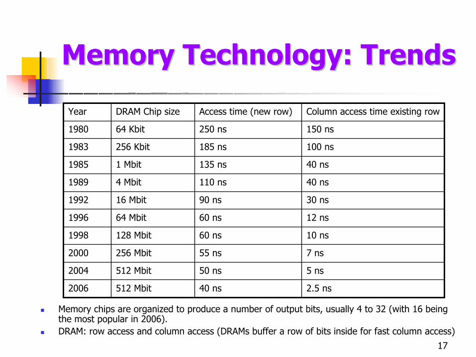
Memory Technology: TrendsMemory Technology: Trends
2.5 ns40 ns512 Mbit2006
5 ns50 ns512 Mbit2004
7 ns55 ns256 Mbit2000
10 ns60 ns128 Mbit1998
12 ns60 ns64 Mbit1996
30 ns90 ns16 Mbit1992
40 ns110 ns4 Mbit1989
40 ns135 ns1 Mbit1985
100 ns185 ns256 Kbit1983
150 ns250 ns64 Kbit1980
Column access time existing rowAccess time (new row)DRAM Chip sizeYear
Memory chips are organized to produce a number of output bits, usually 4 to 32 (with 16 being the most popular in 2006). DRAM: row access and column access (DRAMs buffer a row of bits inside for fast column access)

18
Memory Technology: Memory Technology: DDR SDRAMDDR SDRAM
Recently – DDR SDRAM (double data rate synchronous DRAMs)SDRAM (Synchronous DRAM): provides burst access to data from a series of sequential locations in DRAM. An SDRAM is supplied with a starting address & a burst length; data in burst transferred under control of a clock (e.g. up to 400 MHz in 2006). Advantages of SDRAMs:
Use of clock that eliminates the need to synchronizeElimination of the need to supply successive addresses in the burst
DDR (double data rate) – data transfers on both the leading and the falling edge of the clock (hence twice the bandwidth)To deliver high bandwidth, internal DRAM is organized as interleavedmemory banks
19
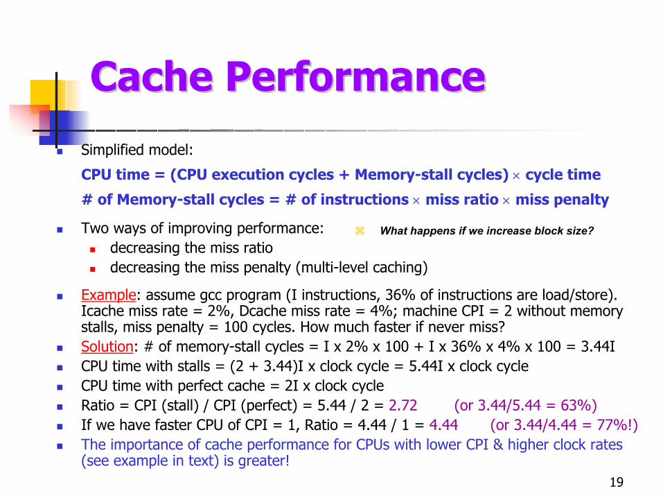
Cache PerformanceCache PerformanceSimplified model:
CPU time = (CPU execution cycles + Memory-stall cycles) × cycle time
# of Memory-stall cycles = # of instructions × miss ratio × miss penalty
Two ways of improving performance:decreasing the miss ratiodecreasing the miss penalty (multi-level caching)
Example: assume gcc program (I instructions, 36% of instructions are load/store).Icache miss rate = 2%, Dcache miss rate = 4%; machine CPI = 2 without memory stalls, miss penalty = 100 cycles. How much faster if never miss?Solution: # of memory-stall cycles = I x 2% x 100 + I x 36% x 4% x 100 = 3.44ICPU time with stalls = (2 + 3.44)I x clock cycle = 5.44I x clock cycleCPU time with perfect cache = 2I x clock cycleRatio = CPI (stall) / CPI (perfect) = 5.44 / 2 = 2.72 (or 3.44/5.44 = 63%)If we have faster CPU of CPI = 1, Ratio = 4.44 / 1 = 4.44 (or 3.44/4.44 = 77%!)The importance of cache performance for CPUs with lower CPI & higher clock rates (see example in text) is greater!
What happens if we increase block size?

20
In direct mappingdirect mapping, a block is placed in exactly one location in cacheIn fully associative mappingfully associative mapping, a block can be in anylocation in the cacheIn n-way set associative mappingset associative mapping, the cache is divided into sets, each consists of n blocks. Each block from memory maps into a unique set in cache given by index field, and the block can be placed in any block of that setAll elements (tags) of the set must be searched to find a match for the block
Compared to direct mapped, n-way set associative cache results in a lower miss ratioIncreasing degree of associativity:
Advantage: decrease miss rateDisadvantage: increase hit time (due to search for match)
Which entry in a set is to be replaced on a miss? Typical solution: Replace the “least recently used” block within the set (LRU replacement strategy)
Set Associative CacheSet Associative Cache
Tag Data Tag Data Tag Data Tag Data Tag Data Tag Data Tag Data Tag Data
Eight-way set associative (fully associative)
Tag Data Tag Data Tag Data Tag DataFour-way set associative
Set01
Tag Data
One-way set associative(direct mapped)
Block0
7
123456
Tag DataTwo-way set associative
Set0123
Tag Data
Example: cache with 8 blocks

21
Example:3 small caches, each 4 1-word blocks. Find number of misses for block sequence 0, 8, 0, 6, 8
Direct mapped cache: 5 misses
2-way set associative:4 misses
Fully associative: 3 misses
AssociativityAssociativity in Caches: in Caches: ExampleExample
Block accessedfrom Memory
Hit / Miss CacheBlock 0
CacheBlock 1
CacheBlock 2
CacheBlock 3
0 miss MemB[0]8 miss MemB[8]0 miss MemB[0]6 miss MemB[0] MemB[6]8 miss MemB[8] MemB[6]
Block accessedfrom Memory
Hit / Miss CacheSet 0
CacheSet 0
CacheSet 1
CacheSet 1
0 miss MemB[0]8 miss MemB[0] MemB[8]0 hit MemB[0] MemB[8]6 miss MemB[0] MemB[6]8 miss MemB[8] MemB[6]
Block accessedfrom Memory
Hit / Miss CacheSet 0
CacheSet 0
CacheSet 0
CacheSet 0
0 miss MemB[0]8 miss MemB[0] MemB[8]0 hit MemB[0] MemB[8]6 miss MemB[0] MemB[8] MemB[6]8 hit MemB[0] MemB[8] MemB[6]

22
44--way Set Associative Cache: way Set Associative Cache: AddressingAddressing
Address
22 8
V TagIndex012
253254255
Data V Tag Data V Tag Data V Tag Data
3222
4-to-1 multiplexor
Hit Data
123891011123031 0
Block offset (assume word addressable, not byte addressable,hence no byte offset)
Compared to direct-mapped cache, set associative cache requires more hardware and even hit access time, but reduces miss rate
23
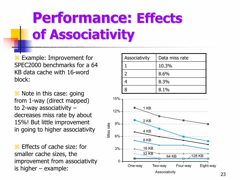
Performance: Performance: EffectsEffectsof of AssociativityAssociativity
Example: Improvement for SPEC2000 benchmarks for a 64 KB data cache with 16-word block:
8.1%8
8.3%4
8.6%2
10.3%1
Data miss rateAssociativity
Note in this case: going from 1-way (direct mapped) to 2-way associativity –decreases miss rate by about 15%! But little improvement in going to higher associativity
Effects of cache size: for smaller cache sizes, the improvement from associativityis higher – example:
Associativity
0One-way Two-way
3%
6%
9%
12%
15%
Four-way Eight-way
1 KB
2 KB
4 KB
8 KB
16 KB32 KB
64 KB 128 KB

24
Multilevel CachesMultilevel CachesAdd a second level cache: Objective is to reduce miss penalty
often primary cache (SRAM) is on the same chip as the processoruse off-chip SRAM for a second level (L2) cache above primary memory (DRAM)miss penalty goes down if data is in L2 cache
CPURegister / Register file
L1Cache
On-chip
L2Cache
SRAM
SRAM
Main(Primary)Memory
DRAM
HardDisk(SecondaryMemory)
MagneticDisk
25
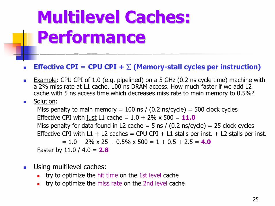
Multilevel Caches: Multilevel Caches: PerformancePerformance
Effective CPI = CPU CPI + ∑ (Memory-stall cycles per instruction)
Example: CPU CPI of 1.0 (e.g. pipelined) on a 5 GHz (0.2 ns cycle time) machine with a 2% miss rate at L1 cache, 100 ns DRAM access. How much faster if we add L2 cache with 5 ns access time which decreases miss rate to main memory to 0.5%?Solution: Miss penalty to main memory = 100 ns / (0.2 ns/cycle) = 500 clock cyclesEffective CPI with just L1 cache = 1.0 + 2% x 500 = 11.0Miss penalty for data found in L2 cache = 5 ns / (0.2 ns/cycle) = 25 clock cyclesEffective CPI with L1 + L2 caches = CPU CPI + L1 stalls per inst. + L2 stalls per inst.
= 1.0 + 2% x 25 + 0.5% x 500 = 1 + 0.5 + 2.5 = 4.0Faster by 11.0 / 4.0 = 2.8
Using multilevel caches:try to optimize the hit time on the 1st level cachetry to optimize the miss rate on the 2nd level cache

26
Virtual Memory (VM)Virtual Memory (VM)
Virtual memoryVirtual memory: Main memory (DRAM) can act as a “cache” for the secondary storage (magnetic disk); a virtual memory block is called a pageAdvantages:
illusion of having more physical memoryprogram relocation (maps virtual addresses from program to physical addresses in memory)
protection
Physical addresses
Disk addresses
Virtual addressesAddress translation
Note: A collection of programs running at once on a machine, total memory required > main memoryMain memory needs to contain only active portions of the many programsPrograms sharing the memory change dynamically

27
Pages: Virtual Memory BlocksPages: Virtual Memory Blocks
Page faultsPage faults: if data not in memory, retrieve them from diskhuge miss penalty, thus pages should be fairly large (typical 4 - 16 KB; new desktop & servers support 32 & 64 KB; new embedded systems are toward 1 KB)reducing page faults is important (LRU is worth, allow full associative placement)can handle the faults in software instead of hardwareusing write-through is too expensive (writes to disk take millions of processor cycles) so we use write-back (copy back)
Address translation (memory mapping)Address translation (memory mapping): CPU produces virtual address, translated by hardware / software to physical address, which can be used to access main memory
3 2 1 011 10 9 815 14 13 1231 30 29 28 27
Page offsetVirtual page number
Virtual address
3 2 1 011 10 9 815 14 13 1229 28 27
Page offsetPhysical page number
Physical address
Translation

28
Much higher miss penalty (millions of cycles)!Large pages [equivalent of cache line] (4 KB to MBs)Associative mapping of pages (typically fully associative)Software handling of misses (but HW handles hits!)Write-through never used, only write-back
Many pagesWith 64 Mbyte memory, 4 Kbytes/pages, have 16 pages
It’s not practical to have 16K comparitorsNor to have software do many comparisons
How can we get virtual memory with full associativity?
How VM Differs from How VM Differs from Memory CachesMemory Caches

29
Implementation: Implementation: Page TablesPage Tables
Physical memory
Disk storage
Valid
111101101101
Page table
Virtual pagenumber
Physical page ordisk address
Page tablePage table: resides in main memory, pointed to by page table registerIndexed with page number from virtual address and contains corresponding physical page number, and valid bit to indicate if page is in main memory Each program has its own page table

30
Page Tables: Address Page Tables: Address TranslationTranslation
Page offsetVirtual page number
Virtua l address
Page offsetPhysical page number
Physical address
Physical page numberValid
If 0 then page is notpresent in memory
Page table register
Page table
20 12
18
31 30 29 28 27 15 14 13 12 11 10 9 8 3 2 1 0
29 28 27 15 14 13 12 11 10 9 8 3 2 1 0
Here:Virtual address space: 232 bytes (4 GB)Physical address space: 230 bytes (memory up to 1 GB)Number of entries in page table: 220
Each entry here needs only 19 bits, but typically rounds up to 32 bits, with extra bits used for additional information & protection

31
Page Tables: Page Faults, Page Tables: Page Faults, Table Sizes, & Write SchemeTable Sizes, & Write Scheme
Page fault: if valid bit in page table is off, a page fault occurs, and operating system gets control to find page in disk and decides where to place page in main memory (LRU or approximate LRU if all pages in memory are in use)
Page table sizes:Example: 32-bit virtual address, 4 KB pages, 4 bytes per page table entry. Page table size = ?Solution: Page offset = 12 bits; number of page table entries = 232 / 212 = 220
Page table size = 220 x 4 = 4 MBPage table uses huge amount of memory --> techniques to limit page table size
Write-back: used for virtual memory due to writes take millions of processor cycles; note also that disk transfer time is small compared with its access time (another advantage of write-back over write-through)A dirty bit is added to page table and set when page is first written, indicating the need to copy back when page is being replaced

32
TLB: TranslationTLB: TranslationLookasideLookaside BufferBuffer
Since page table memory: 1 memory access to get physical address + 1 access to get data ---> slowHence: locality of reference to page table ----> A cache for address translations: TLB(Translation-Lookaside Buffer), which contains a subset of page mappings
TLB is a cache (subset) & therefore must have a tag fieldOn TLB miss, page table must then be examined
Typical TLB:16 - 512 entrieseach block of 1 - 2 entrieshit time of 0.5 - 1 cyclemiss penalty of 10 - 100 cyclesmiss rate of 0.01 - 1%
1111011
11
1
0
0
1000000
11
1
0
0
1001011
11
1
0
0
Physical pageor disk addressValid Dirty Ref
Page table
Physical memory
Virtual pagenumber
Disk storage
111101
011000
111101
Physical pageaddressValid Dirty Ref
TLB
Tag
33
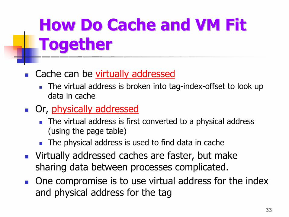
Cache can be virtually addressedThe virtual address is broken into tag-index-offset to look up data in cache
Or, physically addressedThe virtual address is first converted to a physical address (using the page table)The physical address is used to find data in cache
Virtually addressed caches are faster, but make sharing data between processes complicated.One compromise is to use virtual address for the index and physical address for the tag
How Do Cache and VM Fit How Do Cache and VM Fit TogetherTogether
34
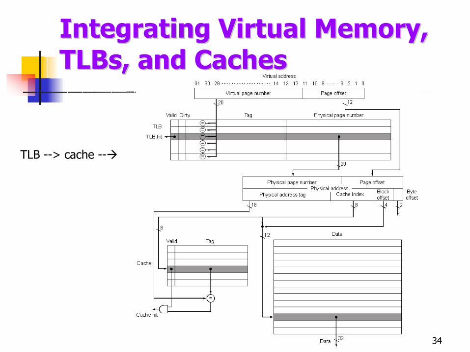
TLB --> cache --
Integrating Virtual Memory, Integrating Virtual Memory, TLBsTLBs, and Caches, and Caches

35
Integrating Virtual Memory, Integrating Virtual Memory, TLBsTLBs, and Caches, and Caches
YesWrite accessbit on?
No
YesCache hit?
No
Write data into cache,update the dirty bit, and
put the data and theaddress into the write buffer
YesTLB hit?
Virtual address
TLB access
Try to read datafrom cache
No
YesWrite?
No
Cache miss stallwhile read block
Deliver datato the CPU
Write protectionexception
YesCache hit?
No
Try to write datato cache
Cache miss stallwhile read block
TLB missexception
Physical address

36
Virtual memory allows sharing of main memory by several processes: need to protect reading / writing of data from one process to another (or to OS)Hardware provide 3 basic capabilities:
Support at least 2 modes: user process or kernel process (supervisor process, OS process, executive process)Provide a portion of CPU state that a user process can read but not writeProvide mechanism for CPU to go from user to supervisor mode, & vice versa
Store page tables in OS’s address space, preventing user processes from changing them
Protection in Virtual MemoryProtection in Virtual Memory

37
Virtual memory providesprotectionsharingperformanceillusion of large main memory
Virtual Memory requires twice as many memory accesses, so we cache page table entries in the TLBFour things can go wrong on a memory access:
cache missTLB miss (but data is found in cache)TLB miss and data misses in cachepage fault
Virtual Memory Key PointsVirtual Memory Key Points

38
Processor speeds continue to increase very fast— much faster than either DRAM or disk access times
Design challenge: dealing with this growing disparity
Paged memory: miss rate < 0.0001% typicallyPage faults take millions of processor cycles, OS will usually select another process to execute in the CPU during disk access
Virtual memory always use fully associative placement while set-associative placement often used by caches & TLBs
Segmentation (variable-size scheme) (vs fixed-size page scheme)
Cache & TLB: physically addressed (at least 2 cache accesses) vs virtually addressed (faster, but more complex)A compromise is virtually addressed cache with physical tags
Virtual Memory: Some IssuesVirtual Memory: Some Issues

39
CPU vs DRAM
Memory: Some DataMemory: Some Data
0.01-2%0.00001-0.0001%0.1 – 2%2 – 5%Miss rates
10-100010 M – 100 M100 - 100010 - 25Miss penalty (cycles)
0.25-16500 MB – 1 TB2 – 3 MB16 – 64 KBSize
Typical for TLB
Typical for paged memory
Typical for L2 cache
Typical for L1 cache
Feature
2006:

40
Memory hierarchy: registers - cache - main memory - diskMemory hierarchy: exploiting locality to try achieve speed of highest level and size of lowest levelSRAMs, DRAMsCache: direct mapped, set assocaitive, fully associativeWrite schemes: write-through, write-backReplacement strategy: LRUMemory interleaving to support cachesCache performance: model, effects of cache sizes, block sizes, associativityMulti-level cachesMemory technologyVirtual memory: page, page faults, write-backPage tables & address translation, TLBsIntegrating virtual memory, TLBs, & caches
Chapter SummaryChapter Summary