memory design - school of engineeringchandy/courses/249s05/249ln15.pdf · memory design •random...
TRANSCRIPT
ECE 249 VLSI Design and Simulation
Spring 2005
Lecture 15
© John A. Chandy
Dept. of Electrical and Computer Engineering
University of Connecticut
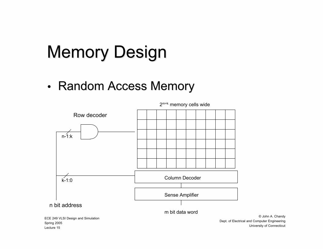
Memory DesignMemory Design
•• Random Access MemoryRandom Access Memory
Row decoder
n bit address
k-1:0
n-1:k
Column Decoder
2m+k memory cells wide
m bit data word
Sense Amplifier
ECE 249 VLSI Design and Simulation
Spring 2005
Lecture 15
© John A. Chandy
Dept. of Electrical and Computer Engineering
University of Connecticut
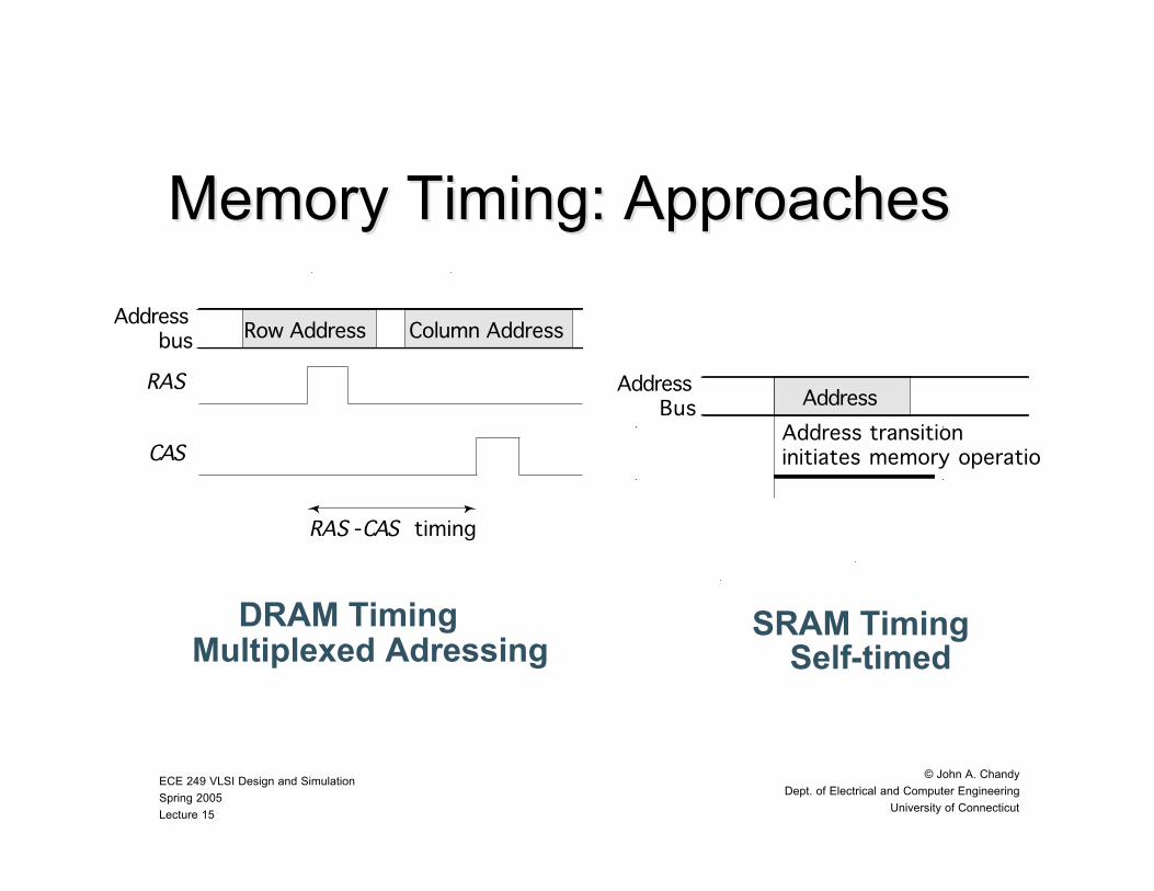
Memory Timing: ApproachesMemory Timing: Approaches
DRAM TimingMultiplexed Adressing
SRAM TimingSelf-timed
Addressbus
RAS
RAS -CAS timing
Row Address
AddressBus
Address transitioninitiates memory operation
Address
Column Address
CAS
ECE 249 VLSI Design and Simulation
Spring 2005
Lecture 15
© John A. Chandy
Dept. of Electrical and Computer Engineering
University of Connecticut
Memory TimingMemory Timing
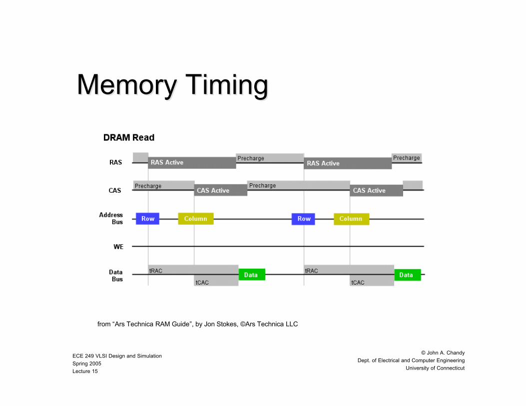
•• DRAM read cycleDRAM read cycle
–– Activate RAS, and place row address on busActivate RAS, and place row address on bus
–– Row decoders select appropriate rowRow decoders select appropriate row
–– Activate CAS, and place column address onActivate CAS, and place column address onbusbus
–– Sense amps are activated and data is placedSense amps are activated and data is placedon the data buson the data bus
ECE 249 VLSI Design and Simulation
Spring 2005
Lecture 15
© John A. Chandy
Dept. of Electrical and Computer Engineering
University of Connecticut
Memory TimingMemory Timing
from “Ars Technica RAM Guide”, by Jon Stokes, ©Ars Technica LLC
ECE 249 VLSI Design and Simulation
Spring 2005
Lecture 15
© John A. Chandy
Dept. of Electrical and Computer Engineering
University of Connecticut
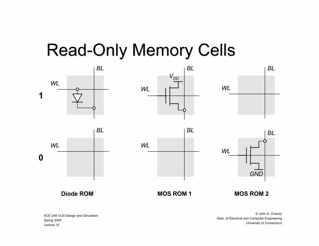
Read-Only Memory CellsRead-Only Memory Cells
WL
BL
WL
BL
1WL
BL
WL
BL
WL
BL
0
VDD
WL
BL
GND
Diode ROM MOS ROM 1 MOS ROM 2
ECE 249 VLSI Design and Simulation
Spring 2005
Lecture 15
© John A. Chandy
Dept. of Electrical and Computer Engineering
University of Connecticut
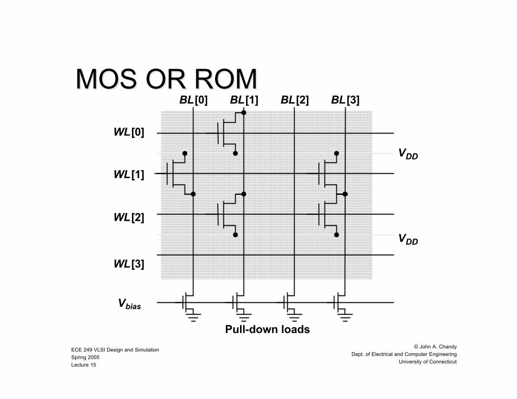
MOS OR ROMMOS OR ROM
WL[0]
VDD
BL[0]
WL[1]
WL[2]
WL[3]
Vbias
BL[1]
Pull-down loads
BL[2] BL[3]
VDD
ECE 249 VLSI Design and Simulation
Spring 2005
Lecture 15
© John A. Chandy
Dept. of Electrical and Computer Engineering
University of Connecticut
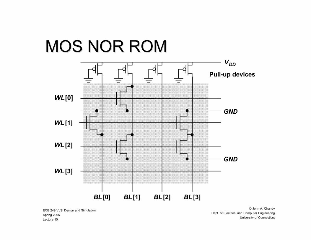
MOS NOR ROMMOS NOR ROM
WL[0]
GND
BL [0]
WL [1]
WL [2]
WL [3]
VDD
BL [1]
Pull-up devices
BL [2] BL [3]
GND
ECE 249 VLSI Design and Simulation
Spring 2005
Lecture 15
© John A. Chandy
Dept. of Electrical and Computer Engineering
University of Connecticut
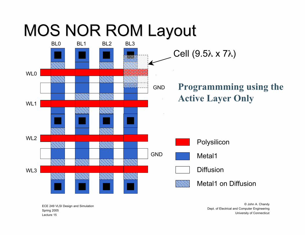
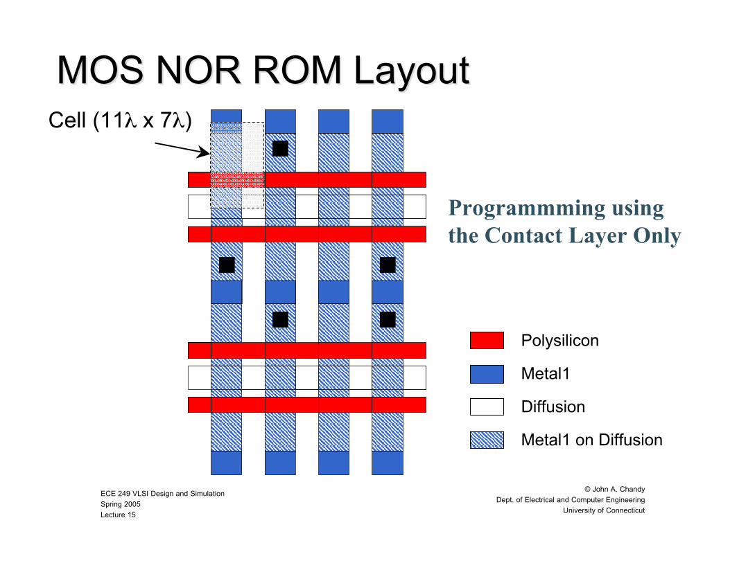
MOS NOR ROM LayoutMOS NOR ROM Layout
Programmming using theActive Layer Only
Polysilicon
Metal1
Diffusion
Metal1 on Diffusion
Cell (9.5λ x 7λ)
GND
GND
WL0
WL1
WL2
WL3
BL0 BL1 BL2 BL3
ECE 249 VLSI Design and Simulation
Spring 2005
Lecture 15
© John A. Chandy
Dept. of Electrical and Computer Engineering
University of Connecticut
MOS NOR ROM LayoutMOS NOR ROM Layout
Polysilicon
Metal1
Diffusion
Metal1 on Diffusion
Cell (11λ x 7λ)
Programmming usingthe Contact Layer Only
ECE 249 VLSI Design and Simulation
Spring 2005
Lecture 15
© John A. Chandy
Dept. of Electrical and Computer Engineering
University of Connecticut
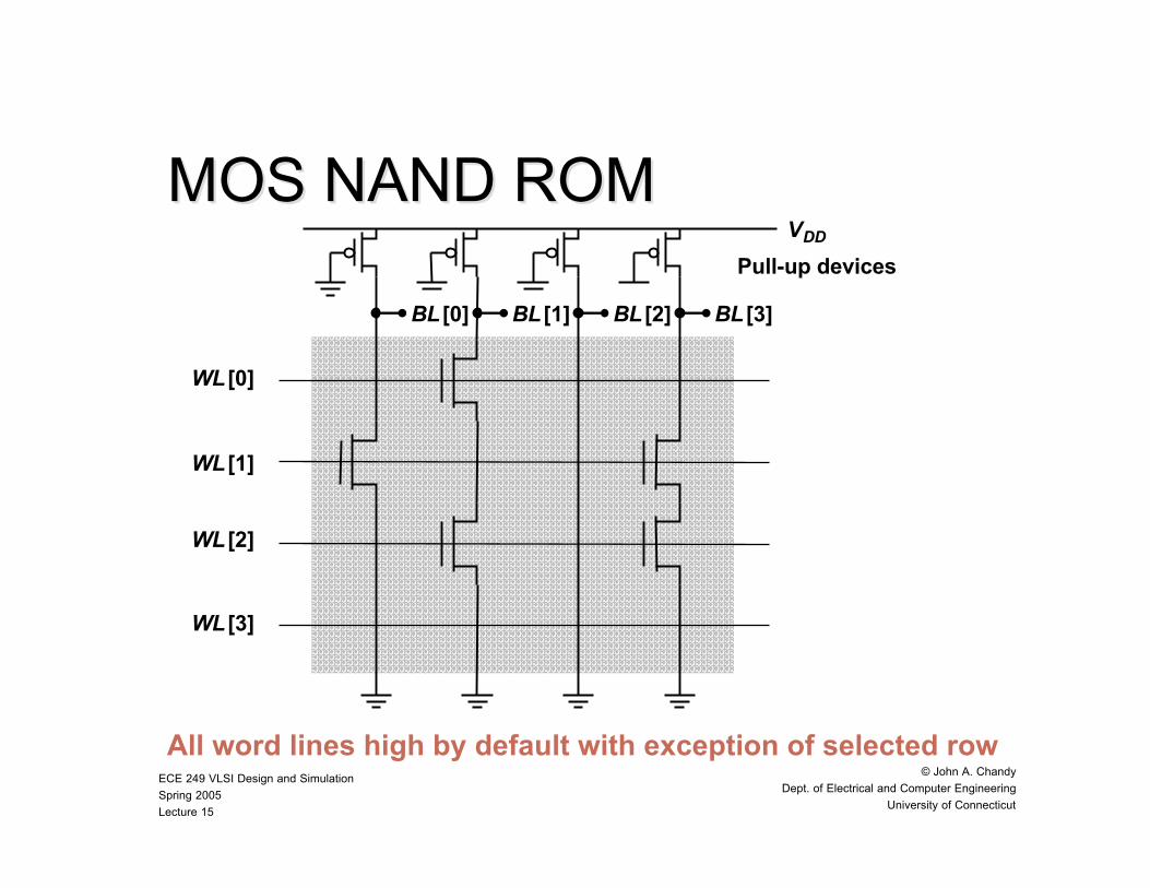
MOS NAND ROMMOS NAND ROM
All word lines high by default with exception of selected row
WL [0]
WL [1]
WL [2]
WL [3]
VDD
Pull-up devices
BL [3]BL [2]BL [1]BL [0]
ECE 249 VLSI Design and Simulation
Spring 2005
Lecture 15
© John A. Chandy
Dept. of Electrical and Computer Engineering
University of Connecticut
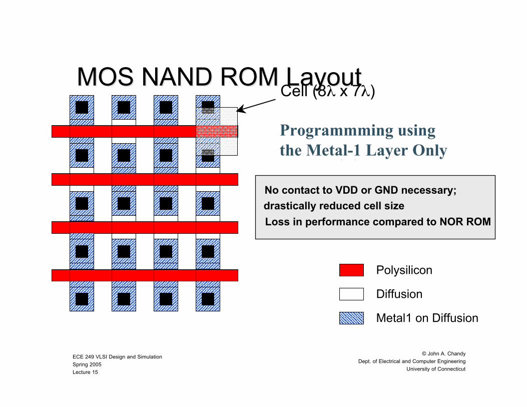
MOS NAND ROM LayoutMOS NAND ROM Layout
No contact to VDD or GND necessary;
Loss in performance compared to NOR ROM
drastically reduced cell size
Polysilicon
Diffusion
Metal1 on Diffusion
Cell (8λ x 7λ)
Programmming usingthe Metal-1 Layer Only
ECE 249 VLSI Design and Simulation
Spring 2005
Lecture 15
© John A. Chandy
Dept. of Electrical and Computer Engineering
University of Connecticut
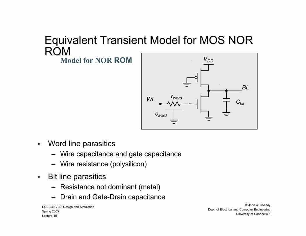
Equivalent TransientEquivalent Transient Model for MOS NOR Model for MOS NORROMROM
•• Word line Word line parasiticsparasitics–– Wire capacitance and gate capacitanceWire capacitance and gate capacitance
–– Wire resistance (Wire resistance (polysiliconpolysilicon))
•• Bit line Bit line parasiticsparasitics–– Resistance not dominant (metal)Resistance not dominant (metal)
–– Drain and Gate-Drain capacitanceDrain and Gate-Drain capacitance
Model for NOR ROM VDD
Cbitrword
cword
WL
BL
ECE 249 VLSI Design and Simulation
Spring 2005
Lecture 15
© John A. Chandy
Dept. of Electrical and Computer Engineering
University of Connecticut
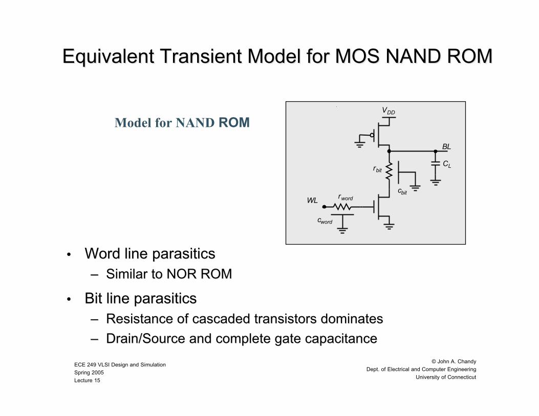
Equivalent Transient Model for MOS NAND ROMEquivalent Transient Model for MOS NAND ROM
•• Word line Word line parasiticsparasitics–– Similar to NOR ROMSimilar to NOR ROM
•• Bit line Bit line parasiticsparasitics–– Resistance of cascaded transistors dominatesResistance of cascaded transistors dominates
–– Drain/Source and complete gate capacitanceDrain/Source and complete gate capacitance
Model for NAND ROMVDD
CL
rword
cword
cbit
rbit
WL
BL
ECE 249 VLSI Design and Simulation
Spring 2005
Lecture 15
© John A. Chandy
Dept. of Electrical and Computer Engineering
University of Connecticut
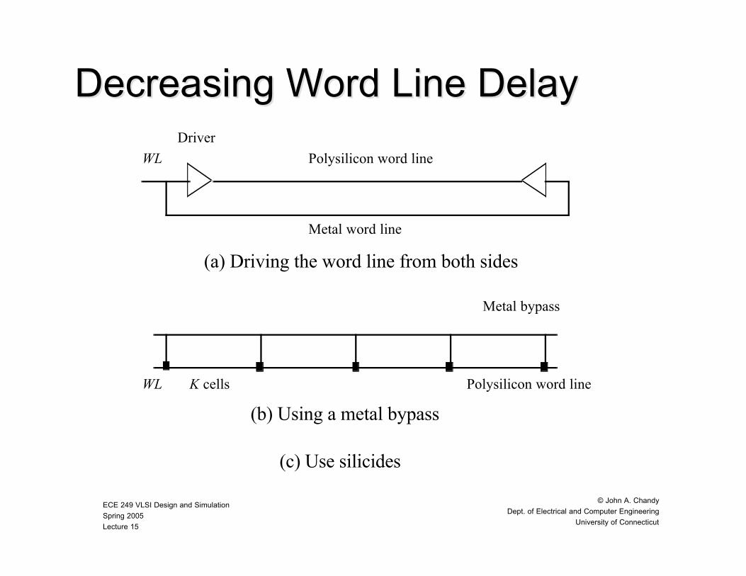
Decreasing Word Line DelayDecreasing Word Line Delay
Metal bypass
Polysilicon word lineK cells
Polysilicon word lineWL
Driver
(b) Using a metal bypass
(a) Driving the word line from both sides
Metal word line
WL
(c) Use silicides
ECE 249 VLSI Design and Simulation
Spring 2005
Lecture 15
© John A. Chandy
Dept. of Electrical and Computer Engineering
University of Connecticut
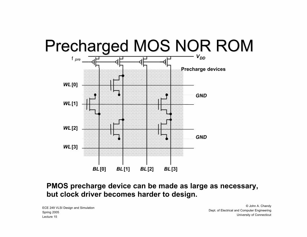
PrechargedPrecharged MOS NOR ROM MOS NOR ROM
PMOS precharge device can be made as large as necessary,but clock driver becomes harder to design.
WL [0]
GND
BL [0]
WL [1]
WL [2]
WL [3]
VDD
BL [1]
Precharge devices
BL [2] BL [3]
GND
pref
ECE 249 VLSI Design and Simulation
Spring 2005
Lecture 15
© John A. Chandy
Dept. of Electrical and Computer Engineering
University of Connecticut
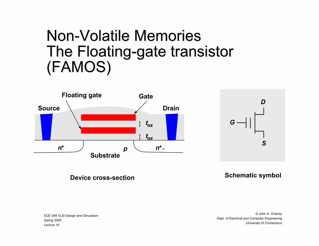
Non-Volatile MemoriesNon-Volatile MemoriesThe Floating-gate transistorThe Floating-gate transistor(FAMOS)(FAMOS)
Floating gate
Source
Substrate
Gate
Drain
n+ n+_p
tox
tox
Device cross-section Schematic symbol
G
S
D
ECE 249 VLSI Design and Simulation
Spring 2005
Lecture 15
© John A. Chandy
Dept. of Electrical and Computer Engineering
University of Connecticut
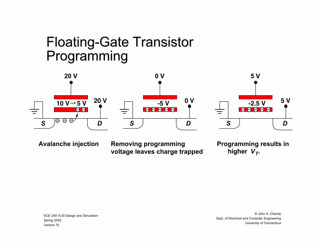
Floating-Gate TransistorFloating-Gate TransistorProgrammingProgramming
0 V
-5 V 0 V
DS
Removing programming voltage leaves charge trapped
5 V
-2.5 V 5 V
DS
Programming results in higher VT.
20 V
10 V 5 V 20 V
DS
Avalanche injection
ECE 249 VLSI Design and Simulation
Spring 2005
Lecture 15
© John A. Chandy
Dept. of Electrical and Computer Engineering
University of Connecticut
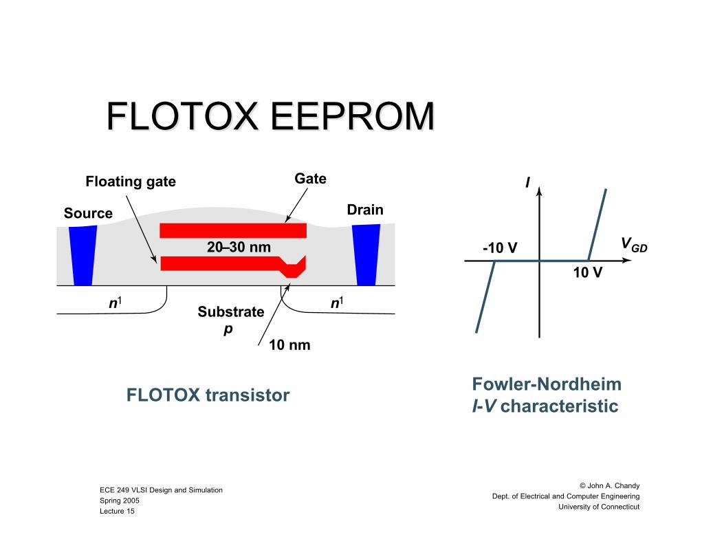
FLOTOX EEPROMFLOTOX EEPROM
Floating gate
Source
Substratep
Gate
Drain
n1 n1
FLOTOX transistorFowler-Nordheim I-V characteristic
20–30 nm
10 nm
-10 V
10 V
I
VGD
ECE 249 VLSI Design and Simulation
Spring 2005
Lecture 15
© John A. Chandy
Dept. of Electrical and Computer Engineering
University of Connecticut
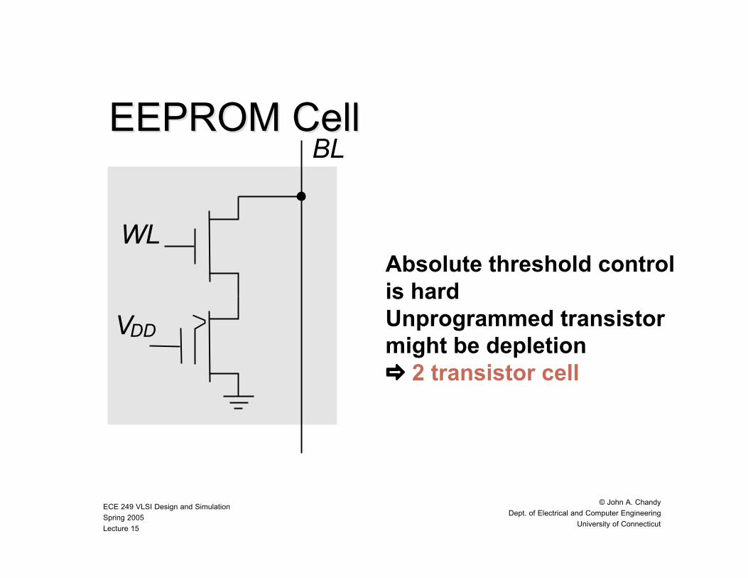
EEPROM CellEEPROM Cell
WL
BL
VDD
Absolute threshold controlis hardUnprogrammed transistor might be depletion 2 transistor cell
ECE 249 VLSI Design and Simulation
Spring 2005
Lecture 15
© John A. Chandy
Dept. of Electrical and Computer Engineering
University of Connecticut
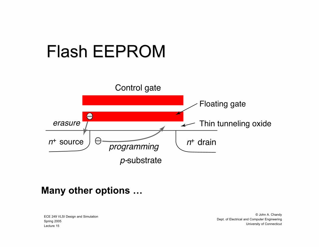
Flash EEPROMFlash EEPROM
Control gate
erasure
p-substrate
Floating gate
Thin tunneling oxide
n+ source n+ drainprogramming
Many other options …
ECE 249 VLSI Design and Simulation
Spring 2005
Lecture 15
© John A. Chandy
Dept. of Electrical and Computer Engineering
University of Connecticut
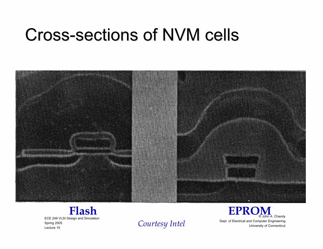
Cross-sections of NVM cellsCross-sections of NVM cells
EPROMFlashCourtesy Intel
ECE 249 VLSI Design and Simulation
Spring 2005
Lecture 15
© John A. Chandy
Dept. of Electrical and Computer Engineering
University of Connecticut
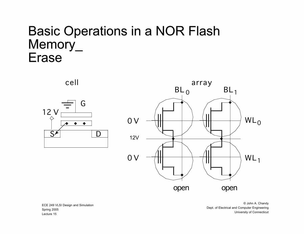
Basic Operations in a NOR FlashBasic Operations in a NOR FlashMemoryMemory__EraseErase
S D
12 VG
cell arrayBL 0 BL1
open open
WL0
WL1
0 V
0 V
12V
ECE 249 VLSI Design and Simulation
Spring 2005
Lecture 15
© John A. Chandy
Dept. of Electrical and Computer Engineering
University of Connecticut
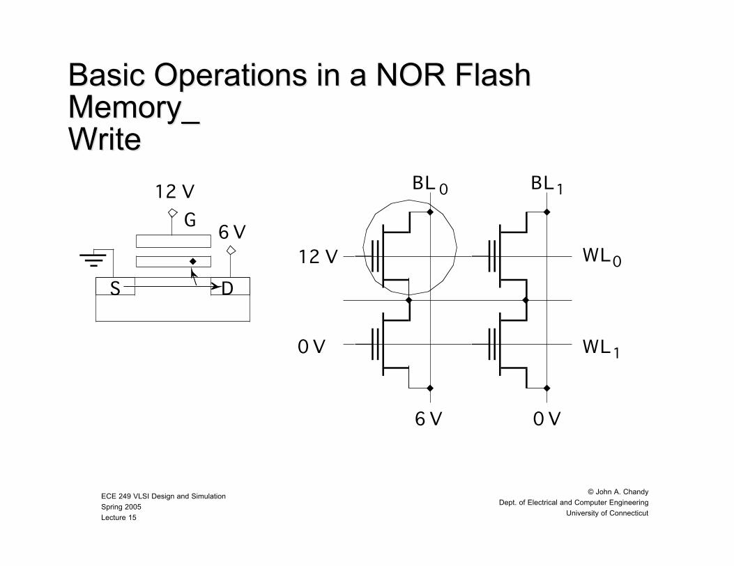
Basic Operations in a NOR FlashBasic Operations in a NOR FlashMemoryMemory__WriteWrite
S D
12 V
6 VG
BL 0 BL1
6 V 0 V
WL0
WL1
12 V
0 V
ECE 249 VLSI Design and Simulation
Spring 2005
Lecture 15
© John A. Chandy
Dept. of Electrical and Computer Engineering
University of Connecticut
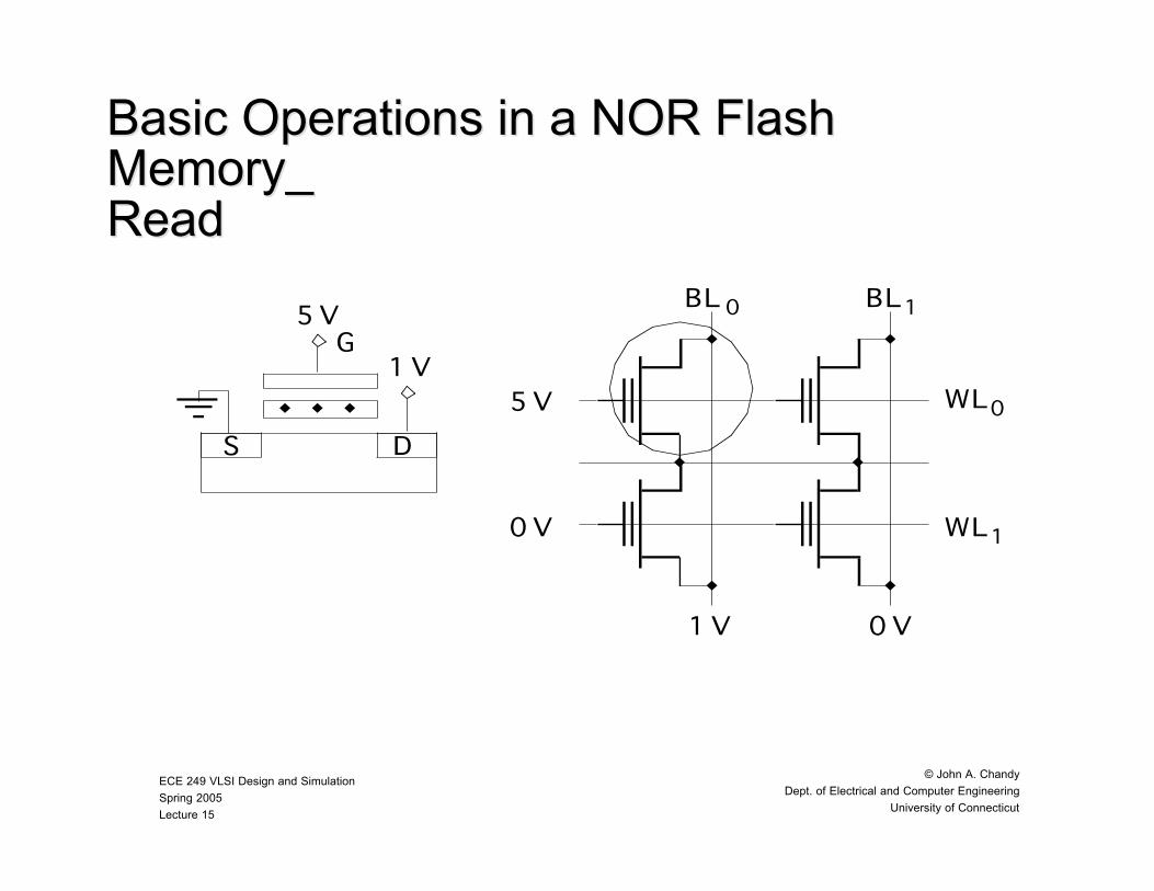
Basic Operations in a NOR FlashBasic Operations in a NOR FlashMemoryMemory__ReadRead
5 V
1 VG
S D
BL 0 BL1
1 V 0 V
WL0
WL1
5 V
0 V
ECE 249 VLSI Design and Simulation
Spring 2005
Lecture 15
© John A. Chandy
Dept. of Electrical and Computer Engineering
University of Connecticut
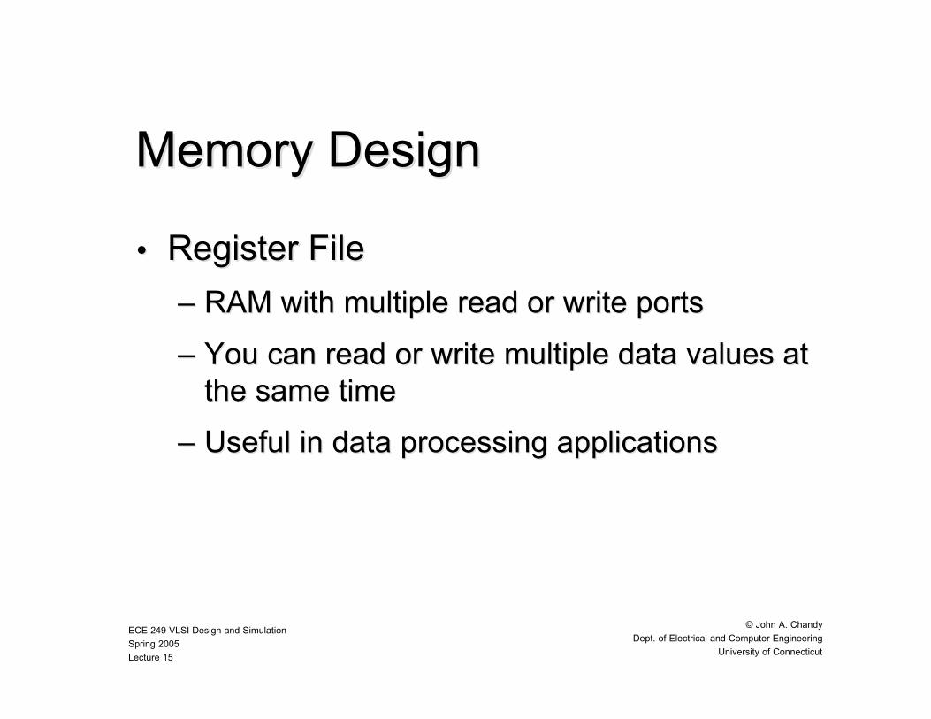
Memory DesignMemory Design
•• Register FileRegister File
–– RAM with multiple read or write portsRAM with multiple read or write ports
–– You can read or write multiple dataYou can read or write multiple data values at values atthe same timethe same time
–– Useful in data processing applicationsUseful in data processing applications
ECE 249 VLSI Design and Simulation
Spring 2005
Lecture 15
© John A. Chandy
Dept. of Electrical and Computer Engineering
University of Connecticut
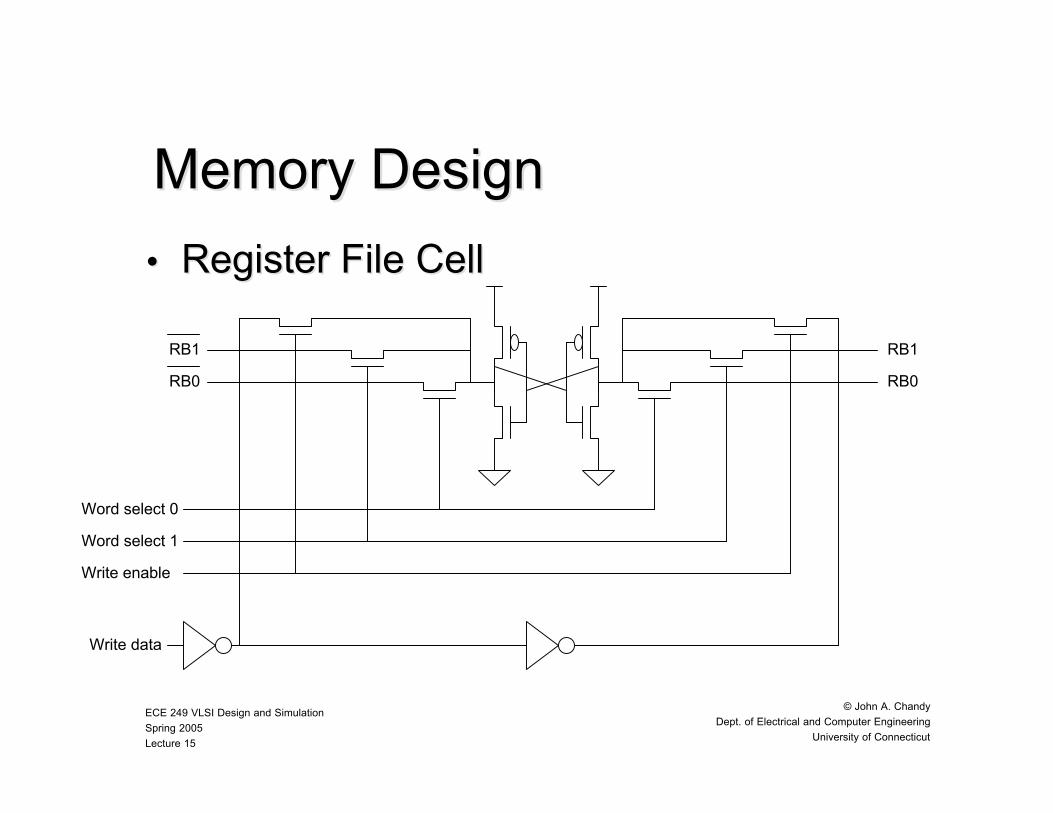
Memory DesignMemory Design
•• Register File CellRegister File Cell
Word select 0
Write enable
Write data
Word select 1
RB1
RB0
RB1
RB0

ECE 249 VLSI Design and Simulation
Spring 2005
Lecture 15
© John A. Chandy
Dept. of Electrical and Computer Engineering
University of Connecticut
Memory DesignMemory Design
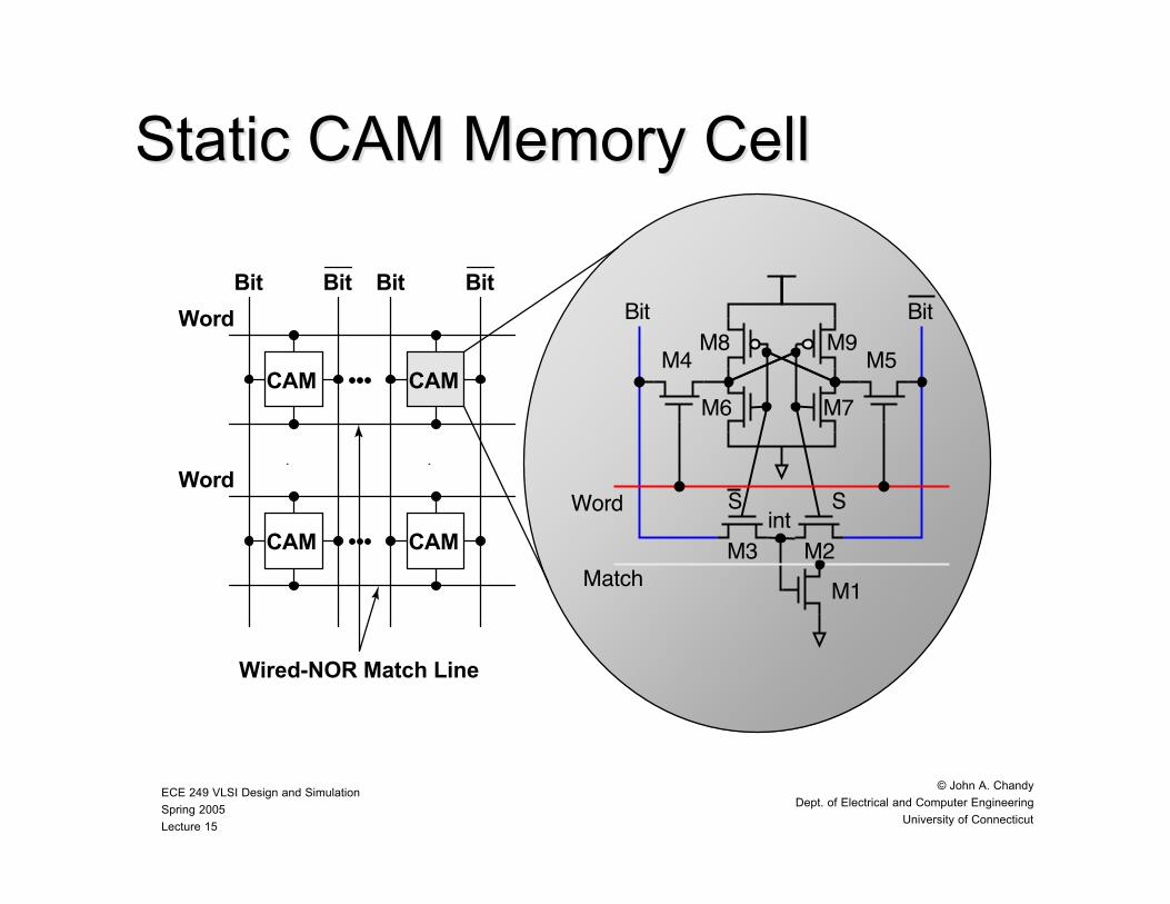
•• Content Addressable Memory (CAM)Content Addressable Memory (CAM)
–– Instead of findingInstead of finding memory by address, find it memory by address, find itby contentby content
–– Search or match every single word inSearch or match every single word inmemory arraymemory array
ECE 249 VLSI Design and Simulation
Spring 2005
Lecture 15
© John A. Chandy
Dept. of Electrical and Computer Engineering
University of Connecticut
Static CAM Memory CellStatic CAM Memory Cell
••• •••
CAM
Bit
Word
Bit
••• CAM
Bit Bit
CAM
Word
Wired-NOR Match Line
Match M1M2
M7M6
M4 M5M8 M9
M3int
SWord••• CAM
Bit Bit
S
ECE 249 VLSI Design and Simulation
Spring 2005
Lecture 15
© John A. Chandy
Dept. of Electrical and Computer Engineering
University of Connecticut
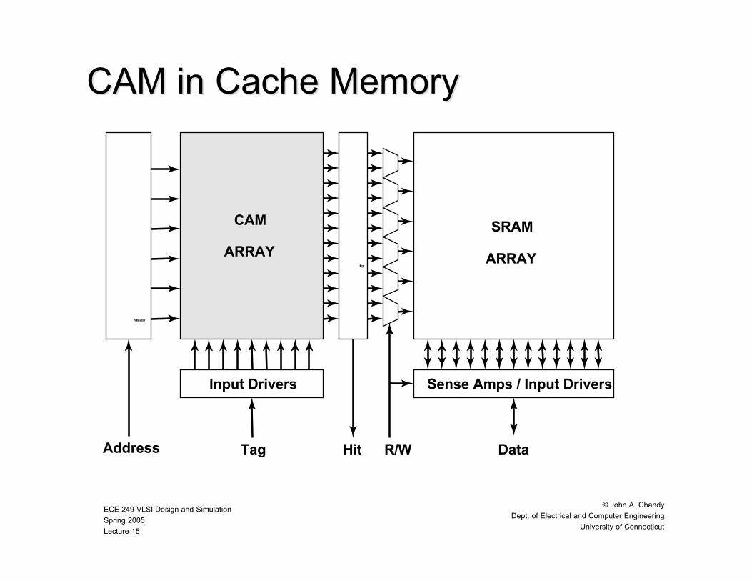
CAM in Cache MemoryCAM in Cache Memory
Address Decoder
Hit Logic
CAM
ARRAY
Input Drivers
Tag HitAddress
SRAM
ARRAY
Sense Amps / Input Drivers
DataR/W
ECE 249 VLSI Design and Simulation
Spring 2005
Lecture 15
© John A. Chandy
Dept. of Electrical and Computer Engineering
University of Connecticut
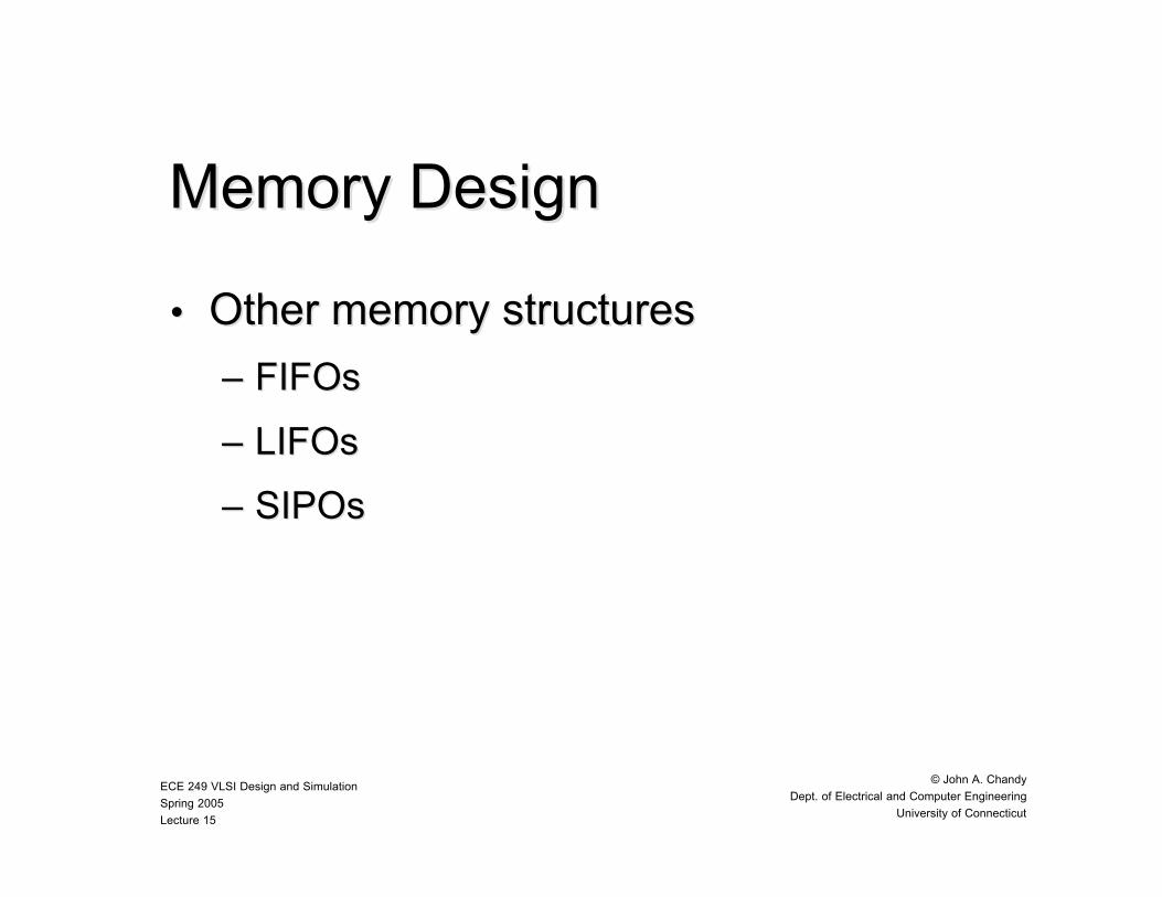
Memory DesignMemory Design
•• Other memory structuresOther memory structures
–– FIFOsFIFOs
–– LIFOsLIFOs
–– SIPOsSIPOs
ECE 249 VLSI Design and Simulation
Spring 2005
Lecture 15
© John A. Chandy
Dept. of Electrical and Computer Engineering
University of Connecticut
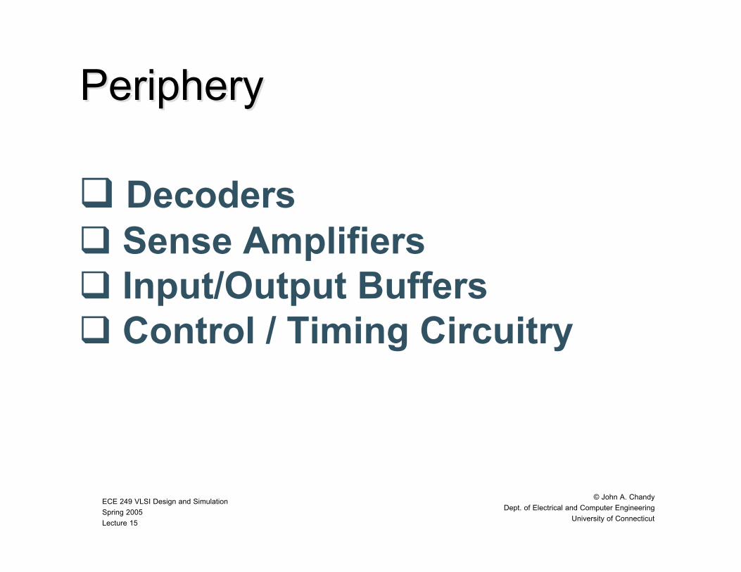
PeripheryPeriphery
Decoders Sense Amplifiers Input/Output Buffers Control / Timing Circuitry
ECE 249 VLSI Design and Simulation
Spring 2005
Lecture 15
© John A. Chandy
Dept. of Electrical and Computer Engineering
University of Connecticut
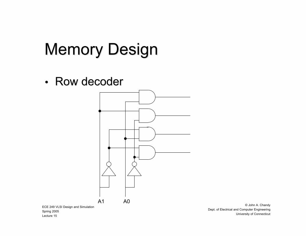
Memory DesignMemory Design
•• Row decoderRow decoder
A1 A0
ECE 249 VLSI Design and Simulation
Spring 2005
Lecture 15
© John A. Chandy
Dept. of Electrical and Computer Engineering
University of Connecticut
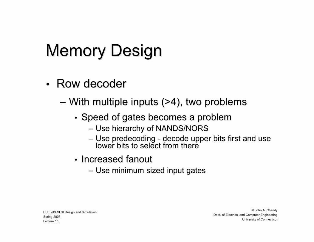
Memory DesignMemory Design
•• Row Row decoderdecoder
–– With multiple inputs (>4), two problemsWith multiple inputs (>4), two problems
•• Speed of gates becomes a problemSpeed of gates becomes a problem–– Use hierarchy of NANDS/NORSUse hierarchy of NANDS/NORS–– Use Use predecoding predecoding - decode upper bits first and use- decode upper bits first and use
lower bits to select from therelower bits to select from there
•• Increased Increased fanoutfanout–– Use minimum sized input gatesUse minimum sized input gates
ECE 249 VLSI Design and Simulation
Spring 2005
Lecture 15
© John A. Chandy
Dept. of Electrical and Computer Engineering
University of Connecticut
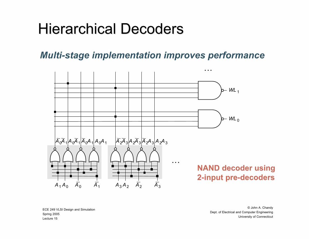
Hierarchical DecodersHierarchical Decoders
• • •
• • •
A2A2
A2A3
WL 0
A2A3A2A3A2A3
A3 A3A0A0
A0A1A0A1A0A1A0A1
A1 A1
WL 1
Multi-stage implementation improves performance
NAND decoder usingNAND decoder using2-input pre-decoders2-input pre-decoders
ECE 249 VLSI Design and Simulation
Spring 2005
Lecture 15
© John A. Chandy
Dept. of Electrical and Computer Engineering
University of Connecticut
Dynamic DecodersDynamic DecodersPrecharge devices
VDD φ
GND
WL3
WL2
WL1
WL0
A0A0
GND
A1A1φ
WL3
A0A0 A1A1
WL 2
WL 1
WL 0
VDD
VDD
VDD
VDD
2-input NOR decoder 2-input NAND decoder
ECE 249 VLSI Design and Simulation
Spring 2005
Lecture 15
© John A. Chandy
Dept. of Electrical and Computer Engineering
University of Connecticut
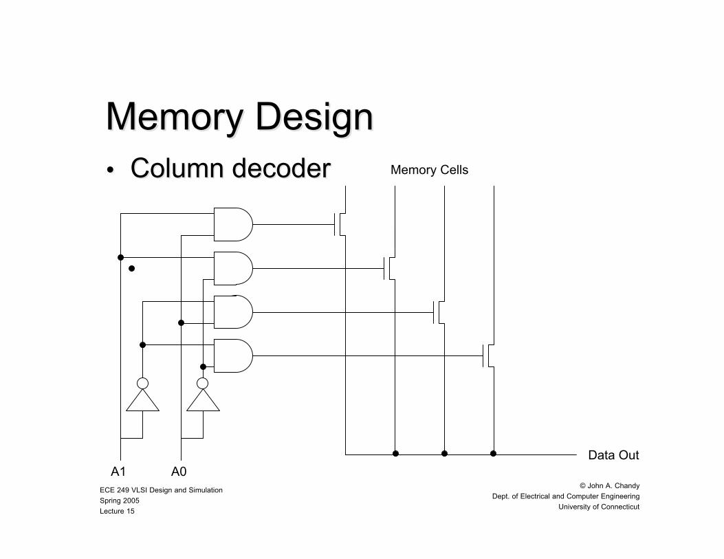
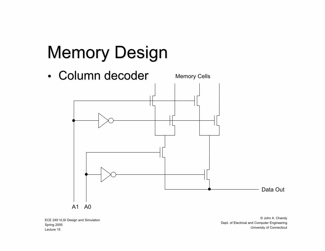
Memory DesignMemory Design•• Column decoderColumn decoder
A1 A0Data Out
Memory Cells
ECE 249 VLSI Design and Simulation
Spring 2005
Lecture 15
© John A. Chandy
Dept. of Electrical and Computer Engineering
University of Connecticut
Memory DesignMemory Design•• Column decoderColumn decoder
A1 A0
Data Out
Memory Cells

ECE 249 VLSI Design and Simulation
Spring 2005
Lecture 15
© John A. Chandy
Dept. of Electrical and Computer Engineering
University of Connecticut
Memory DesignMemory Design
•• Column decoderColumn decoder
–– AND-decoder basedAND-decoder based
•• On the order of NOn the order of N••22NN transistors transistors
–– Binary tree basedBinary tree based
•• Slow because of the series of pass-Slow because of the series of pass-transistorstransistors
–– Usually use a combination of the twoUsually use a combination of the two
ECE 249 VLSI Design and Simulation
Spring 2005
Lecture 15
© John A. Chandy
Dept. of Electrical and Computer Engineering
University of Connecticut
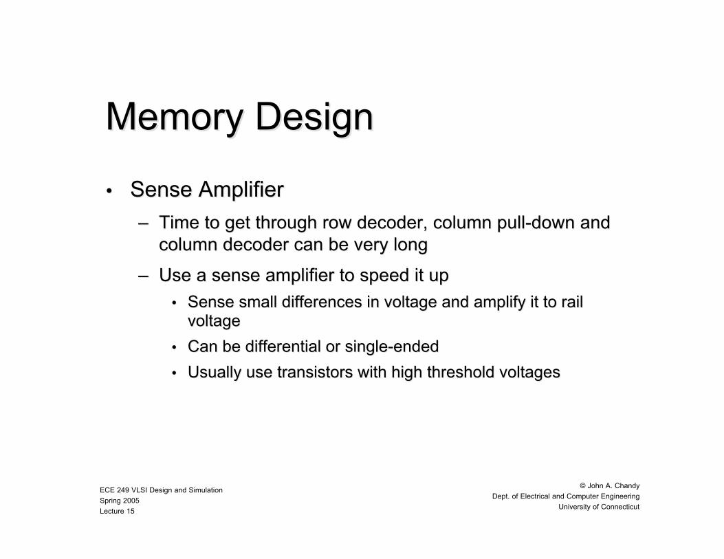
Memory DesignMemory Design
•• Sense AmplifierSense Amplifier
–– Time to get through row decoder, column pull-down andTime to get through row decoder, column pull-down andcolumn decoder can be very longcolumn decoder can be very long
–– Use a sense amplifier to speed it upUse a sense amplifier to speed it up
•• Sense small differences in voltage and amplify it to railSense small differences in voltage and amplify it to railvoltagevoltage
•• Can be differential or single-endedCan be differential or single-ended
•• Usually use transistors with high threshold voltagesUsually use transistors with high threshold voltages
ECE 249 VLSI Design and Simulation
Spring 2005
Lecture 15
© John A. Chandy
Dept. of Electrical and Computer Engineering
University of Connecticut
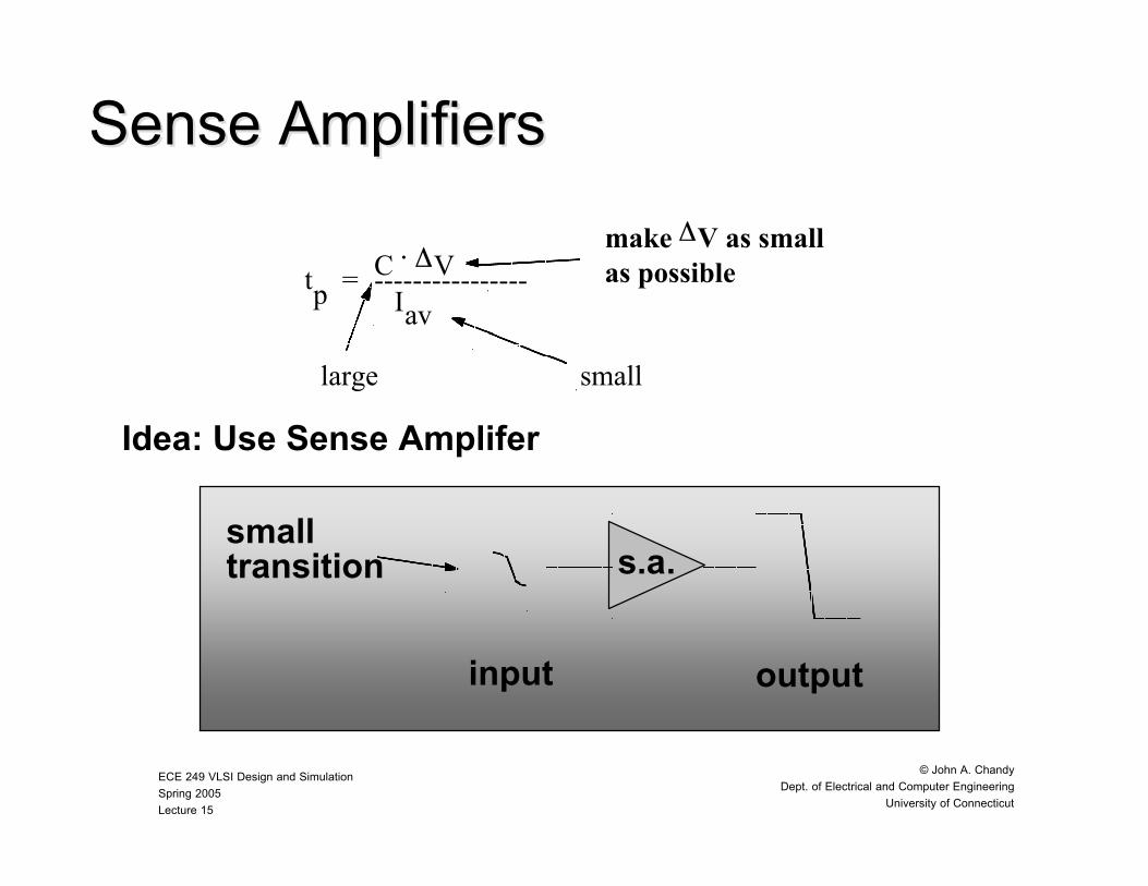
Sense AmplifiersSense Amplifiers
tpC ΔV⋅
Iav----------------=
make ΔV as smallas possible
smalllarge
Idea: Use Sense Amplifer
outputinput
s.a.smalltransition
ECE 249 VLSI Design and Simulation
Spring 2005
Lecture 15
© John A. Chandy
Dept. of Electrical and Computer Engineering
University of Connecticut
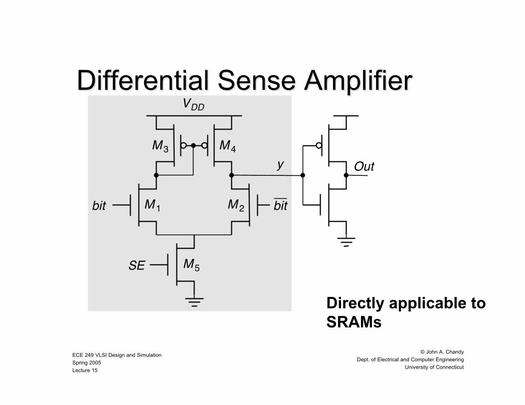
Differential Sense AmplifierDifferential Sense Amplifier
Directly applicable toSRAMs
M 4
M 1
M5
M3
M 2
VDD
bitbit
SE
Outy
ECE 249 VLSI Design and Simulation
Spring 2005
Lecture 15
© John A. Chandy
Dept. of Electrical and Computer Engineering
University of Connecticut
Next classNext class
•• Memory Reliability and YieldMemory Reliability and Yield
•• Control logicControl logic