mems for optical functionalityweb.mit.edu/micronanosystems/www/papers/jeceramic-2004.pdf · mems...
TRANSCRIPT

Journal of Electroceramics, 12, 133–144, 2004C© 2004 Kluwer Academic Publishers. Manufactured in The Netherlands.
MEMS for Optical Functionality
S. KIM, 1 G. BARBASTATHIS 1 & H.L. TULLER 2
1Department of Mechanical Engineering, Microsystems Technology Laboratories, Massachusetts Institute of Technology,Cambridge, MA 02139, USA
2Department of Materials Science and Engineering, Microsystems Technology Laboratories, Massachusetts Institute of Technology,Cambridge, MA 02139, USA
Abstract. We discuss key features of MEMS technology which enable new functionalities of microphotonicdevices, that can by summarized as “arrayability”, i.e. the ability to make massively parallel optical devices in asmall form factor, “reconfigurability,” the ability to change optical properties spatially and temporaly, and “nanopositioning,” the ability to position micro-scale devices with nanometer accuracy. We present an overview of caseswhere a combination of these features has led to commercial successes by creating new optical functionalities, anddiscuss materials-related challenges and future trends for optical MEMS research and commercialization.
Keywords: MEMS, optical functionality, arrayablity, reconfigurability, nano-positioning
1. Introduction
The field of optical micro-electro-mechanical systems(optical MEMS or MOEMS) has experienced rapidgrowth in the recent decade, especially in the late partof the 90’s. The primary application domains, orderedby approximate precedence in embracing MEMS tech-nology, have been: projection displays, componentsfor optical fiber communications (sources, switches,cross-connects, routers, etc.) and optical sensing andimaging. The strong—albeit unsteady—market de-mand, coupled with challenging intellectual problemssparked extensive research and development activitiesin both academia and industry. In tune with these ef-forts were major funding initiatives, first by govern-ments, and subsequently by venture capital and otherprivate investors. Many novel designs, devices, and sys-tems resulted, and some products are in wide com-mercial use today, especially in the projection displaybusiness.
One aspect of MEMS usage in optical systems isminiaturization. This is important in many cases fromthe point of view of footprint and materials costs. How-ever, miniaturization alone could not have been suf-ficient to make optical MEMS technologies commer-cially successful in most cases. The key success factorsof many optical MEMS products have been the new
optical functionalities enabled by the use of MEMS.Among many benefits of MEMS technology that werereviewed as core success factors, the ones that standout are:(1) “arrayability,” which is the term that we use for the
ability to place tiny devices in large-scale arrays;(2) “reconfigurability,” i.e. the ability to reconfigure
the optical properties, spatially and temporally,via localized micro-actuation and/or deformation;and
(3) nanoscale precision control of position and align-ment for microscale devices, which we will referto as “nano positioning.”
Our goal in this paper is to review a few selectedoptical MEMS devices, placing emphasis on the emer-gence of these new functionalities and their impact onoptical products. In Section 2, we begin with a histor-ical introduction, tracing the origins of today’s opticalMEMS devices to solid state research in the 70’s and80’s. We then present a classification of MEMS devicesin Section 3. In Section 4, we describe in some detailselected MEMS product cases, and argue specificallywhy the three functional requirements of arrayability,reconfigurability and nano positioning result in uniquesystem properties. We conclude with some discussionon the future promise and challenges facing opticalMEMS and materials research in Section 5.

134 Kim, Barbastathis and Tuller
2. Historical Background
The first demonstration of a miniature (∼2 × 2 mm)torsional mirror was by Kurt Petersen, while at IBM[1]. Quoting from this paper, Peterson predicts that“. . . silicon micromechanics may eventually find apractical implementation for displays (especially ifsilicon-driving circuitry can be integrated on the samechip, matrix addressing the two-dimensional array ofmirrors-all electronically).” This statement proved tobe truly prophetic, given the current success of MEMSdisplay products such as Texas Instruments’ DigitalMicromirror Device (DMD) [2]. It can also be seen thatmicro-mirror array based displays are one of the oldestthreads in optical MEMS technology [2–5]. The trendled to numerous other applications for micro-mirrorarrays, as we will see later in this paper.
The key idea of a DMD based display is to pro-vide an array of bistable micro-mirrors to intercept thelight path so that one of the mirror positions directs thelight onto a screen, whereas the other position directsthe light onto a block where it is absorbed. Therefore,each mirror modulates a different pixel. By ditheringthe mirror, gray-scaling can be accomplished as well.Color displays can be obtained by standard techniquessuch as a color wheel (most compact and cheapest,and therefore most common) or three mirror arrays(for red-green-blue) combined with dichroic optics andprojected onto the same screen. This technology is dis-cussed in more detail in Section 4.1.
An alternative MEMS display design was proposedin 1994 by a Stanford group, led by David M. Bloom[4]. The modulation concept, as opposed to micro-mirrors, was to modulate the light via diffraction fromminiature gratings, one per pixel on the screen. Thisconcept was termed the “grating light valve” (GLV)by its inventors. The structure and micro-mechanics ofthe GLV are discussed in Section 2.2. In the most com-mon GLV implementation, the light is sent through aSchlieren system which blocks the 0th diffraction orderand lets the ±1st diffraction orders through. So, whenthe grating is inactive there is no light transmitted to thescreen, whereas upon actuation of the grating the cor-responding pixel is illuminated by the interference pat-tern of the +1st and −1st orders. The key difference be-tween the GLV and micro-mirror based displays is thatthe GLV actuators are long (∼0.5 mm) thin (∼few µm)beams alternating between two vertical positions and,hence, can be actuated faster by orders of magnitude(10 s of MHz) than the bulkier torsional micro-mirrors
(typically kHz). Therefore, typically the GLV needs notbe a full 2D pixel matrix, but is instead implemented asa single row, rapidly scanned in the vertical directionto produce the full display. For the same reason, theGLV row can have many more pixels than the lineardimension of a micro-mirror based display of the samegeneration. However, there is a caveat: since the mod-ulation of light is based on diffraction, the efficiencyis reduced, and high-power laser sources are requiredto obtain sufficient brightness (whereas micro-mirrorbased displays work with a simple light bulb.) There-fore, the GLV is naturally targeted towards high-endprojection markets that can afford the price and spacetaken by the bulky laser sources in return for excel-lent resolution of thousands of pixels per dimensionover a large projection area, e.g. digital cinema. Onthe other hand, micro-mirror displays have been suc-cessful at the lower end mass market of computer andvideo projectors, where XGA resolution suffices andprice/footprint/weight are critical factors.
The comparison of DMDs and GLVs is interestingbecause it points out how the intricate relationship be-tween optical principle (reflection vs. diffraction) andmoving parts (tilting rectangular plates vs. thin beamsmoving vertically) can influence seemingly extrane-ous factors (light source selection, resolution, footprint,price) and radically change the outlook of an opticalMEMS product. Interestingly, it is now public infor-mation that Texas Instruments considered alternativemarkets for its DMD product, such as laser printers,before discarding them in favor of the display market[5].
A natural extension of the micro-mirrors themewas what is now known as the “silicon micro-opticalbench,” where optical arrangements were miniaturizedto the surface of a silicon chip, whereas with stan-dard optics they would normally take several squarefeet on an optical table [6]. Several ingenious con-cepts were demonstrated for dealing with light at thesesmall scales, including pop-up micro-mirrors, diffrac-tive micro-lenses (Fresnel zone plates) and on-chipsources [7]. Such optical systems have great potentialin a number of applications such as optical process-ing [8] and sensing [9]. However, the major applica-tion that emerged from these efforts was optical net-working, because it was in that area that the need forminiaturization was the most pressing. Primarily, thetechnology driver was the desire to reduce the size ofa router for a dense wavelength division multiplexing(DWDM) node from that of a large refrigerator to a
MEMS for Optical Functionality 135
briefcase, figuratively speaking. That need was impor-tant not only because such nodes were anticipated tobe placed at central spots in metropolitan areas, wherereal estate is expensive, but also because the capac-ity demand was projected to increase at exponentialrates.
3. Classification of Optical MEMS Devices
Walker and Nagel [10] studied and reviewed MEMStechnologies for optical applications and classifiedthem depending on the types of micro-optics used andoptical functions performed, such as: sources, detec-tors, free space optics, wave guided optics, transmissiveoptics, reflective optics, diffractive optics and interfer-ometric optics as shown in Table 1.
Micromirrors have been used to steer the opticalbeam path through the waveguide, in and out of opticalfibers and to redirect light out of coaxial paths. Manyof the reflective mode MEMS devices have been devel-oped on bare silicon [11], metallic surfaces, and differ-ential index multilayers. The VCSEL (vertical cavitysurface emitting laser) is a typical MEMS device builton differential-index multilayers to achieve high reflec-
Table 1. Key optical devices developed based on MEMS technology.
Devices Products
Reflective mode Micro-mirror array for Texasdevices information displays, instrument’s
Phase correction DMD,piston arrays Daewoo’s TMA
Diffractive mode Fresnel zone plate Silicon Lightoptics Tunable Gratings machine’s GLV
Free space optics 3-D optical switches Optical micro2-D optical switches Machines, Lucent
Lambda router, Xroscross-connect
Waveguide optics Planar waveguideFiber inline alignment
Interference mode Tunable Fabry-Perotdevices external cavity lasers
Detectors Bolometer Honeywell-bolometerarray
Micro-spectrometer PolychromatorTransmission Optical micro shutters
devices and choppersAdaptive optics Deformable mirrors for
aberration correctionSources VCSEL
External cavity laser
tivity [12]. The mirror array has been the most success-ful MEMS application in optics and has been used forprojection displays [2–5], free space optical switching[13] among many others. Diffractive optics has enabledplanar microlenses, Fresnel zoneplate lenses and grat-ings. Efforts have been made to make them tunablein digital [14] or analog manners [15]. In the afore-mentioned devices, light propagates in free space be-fore reaching the actuator, which deflects or diffractsit. An alternative for handling light is to confine it in awaveguide. It then becomes impossible to interact withit directly; however, one can still modify light propa-gation by bringing a MEMS actuator close enough tothe waveguide that light from the waveguide couplesevanescently with the actuator [16, 17, 23]. Typically,evanescent coupling results in phase delay, which inturn can be used for interferometric switching, etc.
Optical MEMS research has demonstrated a largenumber of new devices and systems. Some of the op-tical MEMS devices have become great commercialsuccesses, while many have not. Miniaturization aloneis inadequate to create new markets and/or to becomemore competitive. The most successful optical MEMSdevices commercially have been those, which combineat least two of the three functional requirements among“arrayability,” “reconfigurability” and “nano position-ing.” Some of these successful optical MEMS cases arelisted in Table 1.
4. MEMS Products: Case Studies
The study of optical MEMS technology reveals that thesame basic optical MEMS technology has often beenused for radically different applications, e.g. micro-mirrors for displays versus cross-connects in telecom-munications systems. The reason this broad sharinghas been possible is that the applications share at leastsome of the functional requirements mentioned ear-lier, namely arrayability, reconfigurability, and nano-positioning. In this section, we overview some opticalMEMS products, which emphasize the significance ofthese attributes for commercial success.
4.1. Digital Micromirror Devices (DMD) for DigitalLight Processing (DLP)
In the digital information era, more multimediaapplications require brighter and larger-screen dis-plays as well as compact and personalized displays.
136 Kim, Barbastathis and Tuller
Conventional film projectors cannot display digitalmultimedia information. Many electronic projectiondisplay technologies have been developed since the firstCRT projection display was demonstrated by RCA inthe 1940’s. At present, there are two major projectiondisplay technologies competing in the rapidly grow-ing market: DLP (Digital Light Processing) and high-temperature Poly LCD projection. DLP is very strongin the expensive large venue projector market and low-cost ultra portable projector market, while LCD pro-jection is strong in the middle arena.
The large venue projectors can project more than5,000 ANSI lumens on to a screen and are very ex-pensive, heavy and bulky, and need special care forinstallation and maintenance. 3-chip DLP technologyis dominant in this category given its ability to deliverup to 10,000 lumens of light at much lower cost thanexisting CRT projectors or ILA (Illuminated Light Am-plifier) projectors from Hughes-JVC. The heat gener-ation by light absorption and photo-degradation stilllimits the use of high-power light sources for LCD.The biggest market segment is the so-called portableprojector group and about 95% of projectors in theworld market fall within this category. Currently, themainstream projection technology for this category isthe one-chip DLP. The one-chip DLP engines tend tobe more compact than 3-panel LCD engines, and domi-nate the market with the light weight mobile projectorsunder 3-pounds.
At the core of a digital light-processing projectoris Texas Instrument’s patented Digital Micromirror de-vice (DMD) [2], a MEMS chip with an array of mi-cromirrors mounted on its SRAM surface. Therefore,arrayability is the key optical functionality offered bythe DMD device. Each of these tiny mirrors tilts in re-sponse to electrostatic charges on the mirror’s mount-ing substrate. Depending on the degree of tilt (+10◦, 0◦,−10◦), individual mirrors reflect on/off control of lightfrom the projection lamp. Controlling the duty ratioof on/off stages, 10 bit (1024) grayscales can be cre-ated digitally for each primary color. The color imageis then accomplished with either rotating color wheelswith one DMD chip or dichroic mirrors and combiningprisms with three DMD chips for red, green and blue.Incoming video or graphic signals are turned into a dig-ital code of binary data (0s and 1s) that tilts the DMDmirrors accordingly. By throwing the modulated lightthrough the projection lens with precise digital signalprocessing, a large screen full color image is projectedon to the screen.
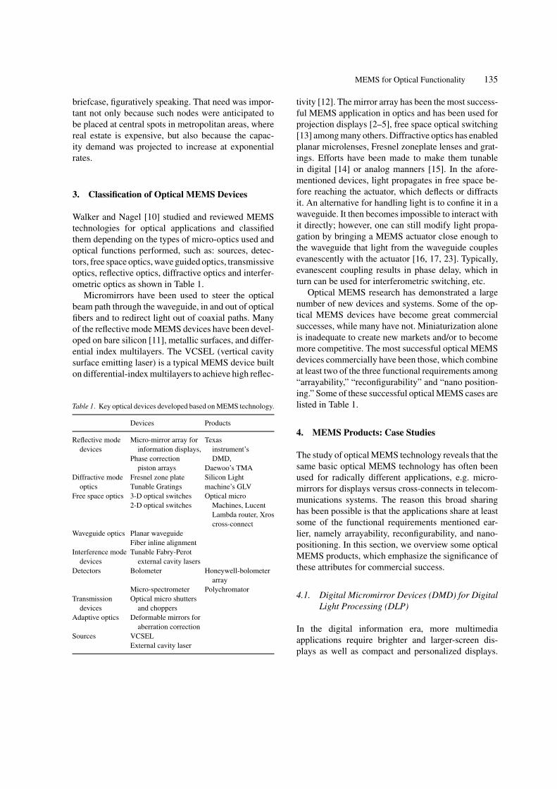
Fig. 1. Two DMD pixels (mirrors are shown as transparent) in op-posite tilting states [2].
The DMD chip has micromirrors on top of a com-pleted CMOS memory circuit as shown in Fig. 1. TheDMD chip is monolithically fabricated by CMOS com-patible processes. Each micromirror switch has an alu-minum mirror, sized 16 µm by 16 µm. The mirror istilted along the hinge in diagonal direction, throughelectrostatic attraction produced at the air gap underthe mirror and on top of the CMOS. The key technicalconcern on the DMD chip has been the issue of me-chanical reliability. Due to the high speed PWM (pulsewidth modulation), the torsional hinge requires relia-bility of more than 1013 cycles through its operatinglife. Hinge failure and hinge memory problems havebeen solved by continuous design improvements overthe last ten years.
4.2. The Thin Film Micromirror Array (TMA)
The Thin-film Micromirror Array (TMA) is a reflec-tive type spatial light modulator fabricated with MEMStechnology [3]. Micromachined thin-film piezoelectricactuators are used to control the tilt angle of each mi-cromirror, which defines the gray scale of the match-ing screen pixel. The light reflected on a mirror surfaceforms a rectangular shaped image on the projectionstop plane and this image moves along the horizontalaxis as the tilt angle changes. When a mirror does nottilt, all of the light reflected by the mirror is blockedand absorbed by the projection stop and the pixel im-age on the screen is in the darkest state (black). Whenthe mirror is fully tilted, all of the light reflected bythe mirror goes out through the projection stop and

MEMS for Optical Functionality 137
the pixel image is in the brightest state (white). Theamount of light that passes through the projection stopis linearly proportional to the tilt angle of each mirror.The precise control of the tilt angle can generate graylevels on the screen in between the brightest and thedarkest state. Therefore, the TMA shares the arrayabil-ity functional requirement with the DMD device, withthe additional functional requirement of nano position-ing of the miniature mirrors to control grayscale. Theapplication of piezoelectric actuation to array MEMStechnology was the key factor for achieving these func-tional requirements.
Each pixel consists of a dual layered structure, amirror layer and an actuator layer. Mirror-tilting is per-formed by thin-film piezoelectric actuators in the formof micro-cantilevers. As shown in Fig. 2, a mirror isconnected to the underlying cantilevers through a sup-port post. The cantilevers are anchored to the underly-ing PMOS substrate. A cantilever consists of the non-stoichiometric silicon nitride (SiNx ) supporting layer,Pt bottom electrode, PZT layer, and top Pt electrode.When an electric field is applied between the two elec-trodes, the piezoelectric layer shrinks in the horizontaldirection and expands in the vertical direction. Sincethe neutral plane of the cantilever shifts toward the bot-tom electrode due to the thickness of the supportinglayer, the mechanical contraction of the piezoelectriclayer causes an upward vertical deflection of the can-tilever and, consequently, the tilting of the mirror ontop of it.
The TMA chip is monolithically fabricated over aPMOS active matrix by surface micromachining tech-niques. The active matrix is a transistor array that ad-dresses the video signal to each pixel. The size of each
Fig. 2. Piezoelectric cantilever-actuated micromirrors for TMA dis-play [3].
mirror is 49 × 49 µm for XGA format TMA chips.The mirror layer is made of aluminum and is sputter-deposited on the second sacrificial layer. The aluminumlayer is patterned to make mirror shapes by a dry etch-ing process. The sacrificial layers are removed to formthe air gaps. Since two different materials are used assacrificial layers, the release process is performed intwo steps. First, the second sacrificial layer is removedthrough the openings between mirrors by plasma etch-ing. After completely removing the second sacrificiallayer, the first sacrificial layer is exposed to air and re-moved by XeF2 vapor etch process. Both release meth-ods show fast lateral etching rates, leave no residues,do not etch or damage the other layers such as Al andPZT. Figure 2 presents the SEM photographs of thecompleted VGA and XGA format TMA chips afterthe release process. The 800,000 finished mirrors in anXGA format TMA chip have initial tilting positions of0◦ ± 0.03◦. A working projector prototype of 5,400 trueANSI lumen was presented at the Asian Display 1998with three TMA chips and a 1 kW Xenon lamp. Theprototype showed overall light transmitting efficiencyof 22%.
TMA’s PZT microcantilever actuators have beenused not only for display, but also for fast-scanningAFM tip arrays [18] and strain-tuning of photonic de-vices [19].
4.3. The Grating Light Valve (GLV)
The GLV is a unique MEMS product that acts as a dy-namic, tunable grating to precisely vary the amount oflaser light that is diffracted or reflected [4, 14]. TheGrating Light Valve is comprised of a series of ribbonson the surface of a silicon chip as shown in Fig. 3, which
Fig. 3. Grating light valve ribbons to form a digitally tunable diffrac-tion grating [4].

138 Kim, Barbastathis and Tuller
can be moved up or down over very small distances bycontrolling the magnitude of electrostatic forces be-tween the ribbons and the substrate. The ribbons arearranged such that each element is capable of eitherreflecting or diffracting light. This allows an array ofelements, when appropriately addressed by control sig-nals, to vary the level of light reflected off the surfaceof the chip. This control of light can be analog (vari-able control of light level) or digital (switching light onor off). Because GLV devices utilize the principle ofdiffraction to switch, attenuate and modulate light, theyare highly accurate, simple to manufacture, and haverelatively high power handling capabilities. However,because the projected light is obtained from diffrac-tion orders rather than direct reflection, some loss ofincident power is inevitably incurred.
Each GLV element consists of six dual-supportedparallel ribbons formed on silicon nitride and coatedwith a reflective top metal layer. The top is used also asan electrical conductor to create electrostatic attractionto the bottom common electrode plane, as shown in thefigure. The on/off switching speed of GLV is as fast as20 nanoseconds, which is much faster than that of exist-ing tilting mirrors. Current GLV devices are claimed tohave a diffraction efficiency near the theoretical maxi-mum of 81%, fill factor of 95% and top layer reflectivityof 91%, with an overall device efficiency of about 70%.This optical efficiency corresponds to an insertion lossof about 1.5 dB.
The large screen projection display has been theprimary target application of GLV technology. It hasbeen demonstrated that a front projection system fora 1,920 × 1,080 HDTV image can be made with thescanning of a linear GLV array of 1080 pixels. How-ever, due to the keen competition between DLP andLCD and the consequent price war in the consumermarket, the need of the additional cost of scanningmechanism and the speckled image resulting from thelaser beam, the commercialization of GLV projectiondisplay has been significantly delayed at the presenttime. However, the digital tunability of GLV has suc-cessfully introduced many reconfigurable optical de-vices, such as reconfigurable blocking filters, dynamicgain equalizers and GLV printers.
4.4. The Polychromator
The Polychromator is an electronically programmable,dark-field correlation spectrometer system based on a
programmable MEMS diffraction grating developedin a joint effort of Honeywell, Massachusetts Instituteof Technology, and Sandia National Laboratory [20].Rather than serving as means for projecting images,the Polychromator is a newly developed sensor capa-ble of distinguishing between a number of differentgaseous species remotely by utilizing a combinationof optics and MEMS. This device provides sufficientsensitivity and selectivity to detect very small amountsof gaseous species for security and biological imagingapplications.
The Polychromator chip does not need a referencecell, which many conventional gas analysis techniquesrequire. Instead, the reference spectrum for each cor-relection measurement is formed by modulating thePolychromator grating. The latter consists of thousandsof mechanical beam elements on a silicon wafer. Thebeams and actuators are manufactured with standardthin film process techniques. Each grating element is10 microns wide and one centimeter long and is de-signed to move up and down as shown in Fig. 4. Lightfrom the environment (e.g., a suspicious “gas cloud”)is directed onto the chip after being collected by anoptical relay, such as a telescope or binoculars. Thegrating is then programmed to “match” the incomingspectrum with a reference spectrum. One thereby de-termines whether the gas cloud contains the substancethat the grating was programmed to match or not. Evi-dently, the key functional requirement in this device isreconfigurability. The Polychromator replaces a bankof gas tanks containing the reference chemicals, whichwould otherwise have to be used to implement corre-lation spectroscopy.
4.5. Uncooled IR Bolometers
Infrared sensors allow objects to be identified and im-aged according to their body temperatures. The abilityto image by temperature allows for remote thermome-try and the ability to see through darkness, smoke andinclement weather. Until recently, high performancecameras have required expensive cooling to cryogenictemperatures to detect photons and to suppress thermalnoise. More recently, detectors operating at room tem-perature have been developed using micromachinedbolometers and pyroelectric detectors. Uncooled in-frared FPA (focal plane array) structures can imageinfrared scenes generated by humans and objects bytransforming the induced temperature changes in the
MEMS for Optical Functionality 139
Fig. 4. Polychromator developed by MIT, Sandia and Honeywell [20].
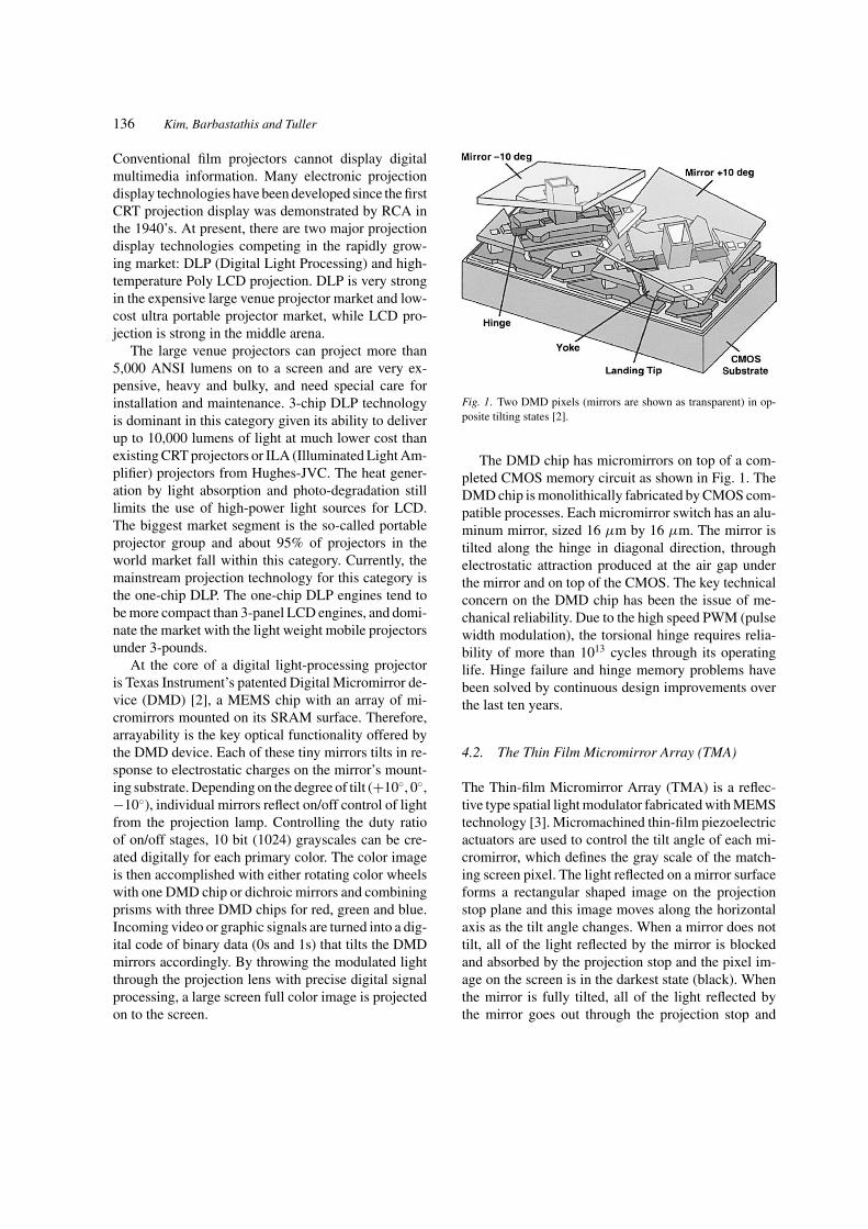
detectors into electrical signals. Uncooled bolometersutilize the temperature-induced changes in electricalresistance, polarization, and dielectric properties of thedetector materials.
Detectors on uncooled FPAs need high thermal iso-lation from the substrate to achieve high sensitivity.MEMS technology plays a key role in enabling thefabrication of very low thermal mass detectors withexceptionally high thermal isolation. Wood and col-leagues [21] fabricated a 2-dimensional array of re-sistive bolometers with the thermal isolation structureas shown in Fig. 5. The silicon nitride membrane, sup-ported by two tethers, floats above the silicon substrate.The size of the tether was adjusted to provide a thermalconductance of 8 × 10⁻⁸ W/◦K. The thermal mass ofthe plate was 8 × 10⁻¹⁰ J/◦K and the thermal responsetime was 10 msec. Operating at 30 frames per secondwith f/1 optics, the measured NETD (noise equivalenttemperature difference) was 0.04◦C with vanadium ox-ide as the resistive material. Honeywell has commer-
Fig. 5. Uncooled bolometer pixel (coplanar design by Honeywell)[21].
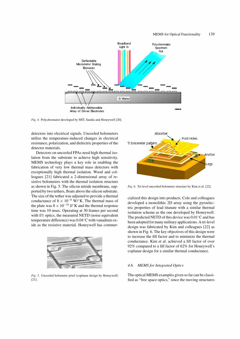
Fig. 6. Tri-level uncooled bolometer structure by Kim et al. [22].
cialized this design into products. Cole and colleaguesdeveloped a monolithic 2D array using the pyroelec-tric properties of lead titanate with a similar thermalisolation scheme as the one developed by Honeywell.The predicted NETD of this device was 0.01◦C and hasbeen adopted for many military applications. A tri-leveldesign was fabricated by Kim and colleagues [22] asshown in Fig. 6. The key objectives of this design wereto increase the fill factor and to minimize the thermalconductance. Kim et al. achieved a fill factor of over92% compared to a fill factor of 62% for Honeywell’scoplanar design for a similar thermal conductance.
4.6. MEMS for Integrated Optics
The optical MEMS examples given so far can be classi-fied as “free space optics,” since the moving structures

140 Kim, Barbastathis and Tuller
Fig. 7. MEMS for switching and tuning of integrated optics. (a) A bridge structure and (b) a cantilever suspended over an optical waveguidechange the mode shape, resulting in phase shift of the guided light [23].
(mirrors, grating beams, etc.) interact with light in itsfree space propagation (radiation) mode. By contrast,light in integrated optics is confined to optical waveg-uides laid out on top of a proper optical material, asshown in Fig. 7. In this case, it is clearly difficult to con-trol light propagation by means of mirrors or diffractiongratings in direct contact with the light beam. However,an alternative means of controlling light via mechan-ical structures in integrated optics still exists, basedon evanescent coupling between the guided light anddielectric structures such as bridges or cantilevers sus-pended over the waveguide [23]. These structures arebasically phase modulators, and they work by alter-ing the effective refractive index of the waveguide and,hence, the group velocity of light. The demonstrationreported in reference [23] was a 2 × 2 optical switchof the Mach-Zehnder interferometer type, where thephase delay was controlled by the MEMS device viathe aforementioned phase modulation property, as op-posed to the typical thermo-optic effect.
4.7. Tunable Fabry-Perot Cavities
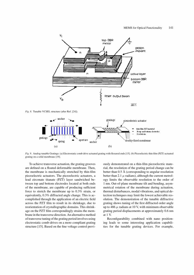
The “nano positioning” functionality is critical for ap-plications such as tunable laser cavities, where the cav-ity length specifies the lasing wavelength. This require-ment led to a successful marriage between the posi-tioning capabilities of MEMS and the Vertical CavitySurface Emitting Laser (VCSEL) technology [24]. VC-SELs had been invented earlier [25–27] as a means toget solid state lasers to emit light in the vertical direc-tion with respect to the substrate, which is preferablefor numerous applications in illumination, optical in-
terconnects, etc. In the original design, the top reflec-tor of the VCSEL device was a distributed Bragg re-flector (DBR) structure. In the MEMS implementation[24], the reflector was attached to a movable cantileverstructure which was capable of tuning the resonancewavelength by as much as 15 nm with a low actua-tion voltage, approximately 5.7 V (Fig. 8). Since thesefirst attempts, tunability has improved to cover the en-tire 1530–1620 nm range of dense wavelength divisionmultiplexing (DWDM) communications [25].
4.8. Strain-Tunable Optical Devices
Tunable gratings such as the GLV and the Polychroma-tor can be described as “digital,” since actuation resultsin change of the grating period and modulation profileby discrete amounts, equal to the size of the microma-chined ribbons. Therefore, reconfigurability is limitedby the smallest feature size that the available lithogra-phy can deliver in a structurally sound configuration.To cover the range of reconfigurability at ultra smallscales, a new class of “analog” tunable gratings hasbeen developed [15, 19]. Nano-positioning is an addi-tional functionality offered by these devices, necessaryfor reconfiguration to be as accurate as necessary foroptical applications. However, another aspect of recon-figurability is sacrificed: e.g., these analog devices can-not perform the polychromator function in a correlationspectrometer. Analog tuning of a diffractive grating isachieved by transverse actuation of the grating struc-ture using thin-film piezoelectric actuators [15, 19] orelectrostatic comb drives with flexured gratings [15],as illustrated in Fig. 9.
MEMS for Optical Functionality 141
Fig. 8. Tunable VCSEL structure (after Ref. [24]).
Fig. 9. Analog-tunable Gratings: (a) Electrostatic comb drive actuated grating with flexured ends [15]. (b) Piezoelectric thin film (PZT) actuatedgrating on a solid membrane [19].
To achieve transverse actuation, the grating groovesare defined on a floated deformable membrane. Then,the membrane is mechanically stretched by thin-filmpiezoelectric actuators. The piezoelectric actuators, alead zirconate titanate (PZT) layer sandwiched be-tween top and bottom electrodes located at both endsof the membrane, are capable of producing sufficientforce to stretch the membrane up to 0.3% strain, orequivalently, 0.3% diffracted angle change. This is ac-complished through the application of an electric fieldacross the PZT film to result in its shrinkage, due toreorientation of crystallographic domains. This shrink-age on the PZT film correspondingly strains the mem-brane in the transverse direction. An alternative methodof transverse tuning of the grating period involves usingelectrostatic comb-drives on a more compliant gratingstructure [15]. Based on the fine voltage control previ-
ously demonstrated on a thin-film piezoelectric mate-rial, the resolution of the grating period change can bebetter than 0.5 A (corresponding to angular resolutionbetter than 2.1 µ radians), although the current metrol-ogy limits the observable resolution to the order of1 nm. Out-of-plane membrane tilt and bending, asym-metrical rotation of the membrane during actuation,thermal disturbances, modal vibrations, and optical de-tection techniques may limit the lowest achievable res-olution. The demonstration of the tunable diffractivegrating shows tuning of the first diffracted order angleup to 486 µ radians at 10 V, with minimum observablegrating period displacements at approximately 0.6 nmat 1 V.
Reconfigurability combined with nano position-ing leads to some interesting application capabili-ties for the tunable grating devices. For example,

142 Kim, Barbastathis and Tuller
using ultra-precise tunable gratings one can compen-sate for thermal detuning in wavelength-sensitive op-tical networking elements such as wavelength multi-plexers/demultiplexers and routers. Another intriguingpossibility is the concept of “optical diversity,” whichwe have developed to compensate for the aperture limi-tation in grating-based spectrometers. This is describedin more detail in the next paragraph. It should also benoted that arrayability is possible for the grating de-vices, especially the piezoelectric version where theactuators occupy smaller real estate surrounding theactive grating area, compared to the electrostatic ver-sion.
Optical diversity is motivated by a challenge thatminiaturization often poses to optical devices: the lim-ited optical aperture. Briefly, the problem is posed asfollows: the spectral resolution in a grating spectrom-eter is determined by the number of periods N that thegrating is composed of. Since the available area in aminiature spectrometer is, by definition, small, the ac-quired spectra can get “blurred.” In other words, themeasured value of spectral density at a given wave-length returned by the spectrometer does not corre-spond to the true spectral density at that wavelength ofthe specimen that is being tested (e.g. a potentially dan-gerous chemical) but also contains contributions fromother neighboring wavelengths. The mathematical op-eration describing the blurring of the measured spec-trum is a convolution of the true spectrum with theimpulse response of the grating. The impulse responseturns out to depend on N , as well as the quality of thecollector optics that relay light from the specimen to thegrating. The effect of the convolution can be undone bythe inverse operation, namely a deconvolution, whichcan be performed digitally by post-processing the mea-sured spectra. However, the deconvolution process ishighly sensitive to noise that is unavoidably present inany measurement. It has been discovered that, by tuningthe grating and repeating the spectral measurement, wecan recover the blurred spectra with much less sensitiv-ity to noise and, consequently, much higher accuracythan a single blurred measurement would allow.
Optical diversity works as follows: the grating pe-riod is first set to an initial value and a blurred measure-ment is taken. Then the grating is actuated so that theperiod changes by a small amount, and a new mea-surement, also blurred, is taken. The process is re-peated, depending on the amount of noise present inthe measurements—the lower the signal-to-noise ratio,the larger the number of necessary measurements. The
ensemble of blurred measurements thus collected issubsequently processed using a class of mathematicaltechniques called “regularized pseudo-inverse” [29].After this step, the final de-blurred spectrum is ac-quired. The quality of the spectrum de-blurring processis determined by the noise present in the measurementsand also by the precision and accuracy of grating ac-tuation. Thus, optical diversity is a good example ofhow reconfigurability and nano-positioning help solvea significant optical problem stemming from miniatur-ization of an optical spectrometer system.
5. Materials Challenges in OpticalMEMS Devices
Micromachining enables the fabrication of miniaturemovable structures ideally suited for applications in theoptical domain. Small mechanical displacements, e.g.a quarter wavelength in an interferometer can produceon-off switching or create modulation effects strongerthan in conventional electrooptic or free carrier acti-vated devices. Likewise, arrays of micromirrors canserve as the basis of displays and of optical cross-connects as discussed above. At the same time, theseminiature MOEMS structures must satisfy certain di-mensional and structural constraints which may beless important for other MEMS applications. For ex-ample, surface roughness determines mirror reflectiv-ity while stressed membranes distort reflected opticalimages. Waveguides integrated within MOEMS mustexhibit reproducible indices of refraction and opticallosses. Actuators, whether electrostatic, piezoelectricor thermal-mechanical, require low voltage operation,power dissipation and chip real estate, all the whileoperating reproducibly over many switching cycles.Other chapters in this special issue focus, in some de-tail, on MEMS processing issues. In the following, wemention aspects of particular importance for MOEMSdevices.
A prime example of the special materials and fab-rication requirements of MOEMS is the DMD pro-jection display chip developed by Texas Instruments(TI). Instead of utilizing the conventional surface mi-cromachining process utilizing phosphosilicate glassfor the sacrificial layers and polysilicon for the mi-cromechanical elements, TI developed a low tempera-ture process utilizing conventional positive photoresistand sputter deposited aluminum alloys [30]. This en-ables fabrication of all the underlying electronic and

MEMS for Optical Functionality 143
micromechanical components beneath the micromir-rors thereby imparting a high fill factor and small mir-ror gaps. To insure high reliability, special attention wasdirected towards minimizing stiction between contact-ing parts, hinge memory and sensitivity to particulates.For the former, a self-assembled monolayer lubricantis applied to lower adhesion forces. In addition, feed-back electronics are utilized to monitor and control themovement of the mirrors to eliminate overshoot andoscillations to further protect against stiction [31]. Alow creep Al alloy was developed to minimize shifts inmicromirror angle with time. Packaging was assignedto class 10 rather than class 10,000 clean rooms to elim-inate failures due to foreign particles, keeping in mindthat these devices contain more than one million mi-cromechanical elements and that the eye can readilydetect even a few faulty pixels within the display.
Microcantilever beams, membranes and micro-bridges are often stressed, particularly when thin filmsare deposited onto these structures. The stresses maybe of an intrinsic nature (e.g. lattice mismatch) or dueto thermal-mechanical stresses resulting from differ-ences in thermal expansion coefficients. This forcesstructures out of plane, often at unpredictable angles.Indeed, Chen et al. [32] proposed a 2×2 optical switchbased on a polysilicon microcantilever beam with at-tached hinged micromirror which is normally out ofplane due to a Cr-Au layer which places the polysili-con under compressive stress. The switch is actuated byapplying a voltage between the cantilever and the sub-strate thereby bringing the mirror into the optical pathlength of the integrated optical fibers. The micromir-rors used in telecommunication for signal routing aretypically coated with gold for its excellent reflectingproperties in the IR. However, since Au serves as a deeptrap in silicon, great care must be taken to avoid poison-ing the electronic devices integrated into the structure[33].
Silicon nitride is often used to fabricate opticalwaveguides by a variety of techniques including sput-tering, CVD, PECVD and LPCVD. Both the gen-eral method used and the detailed processing condi-tions contribute to variations in index of refraction n,optical loss and the magnitude and nature of resid-ual stresses. For example, utilizing PECVD, one finds1.9 < n < 2.2 and stresses range from tensile to com-pressive depending on the Si/N ratio and the depositionconditions [32]. Thus, both the choice of materials andthe processing conditions must be carefully controlledto ensure reproducible and stable structures.
In addition to passive optical materials such asSi3N4, active materials such as electrooptic and magne-tooptic materials are of interest for optical modulation,pyroelectric materials for IR sensing and fluorescentmaterials as light sources. Other active materials ofinterest include piezoelectric materials such as PZT.The majority of such materials are complex oxides,often with the perovskite or garnet structure and nor-mally, in the bulk state, require very high temperaturesto achieve desired phase purity and microstructure. Toenable integration with silicon based microelectronicand/or MEMS chips, these materials are prepared asthin films either by vapor phase techniques (e.g. sput-tering, PLD, MOCVD, MBE) or chemical routes (e.g.sol gel). In general, the degree of crystallinity andorientation, microstructure, stoichiometry and built instress depend sensitively on the deposition conditions,type and temperature of substrate during deposition andsubsequent annealing conditions. In general, the filmsshow reduced activity compared to their bulk coun-terparts. For example, an electrooptic modulator pre-pared by deposition of BaTiO3 films onto an MgO sin-gle crystal substrate exhibited an effective electroop-tic coefficient of 50 pm/V [34], less than an order ofmagnitude lower than the maximum value measuredfor single crystals [35]. Similar effects are often notedfor piezoelectrics with reduced effective piezoelectriccoefficients. These are suspected to be related to con-straints imposed by the substrate, and by defects andother interfaces. Buffer layers, between silicon and theactive oxides are essential to prevent interdiffussionand oxidation and also serve as seed layers to aid inthe nucleation of the appropriate phases and crystallo-graphic orientations. An excellent review of many ofthese issues may be found in the article by Muralt [36].
6. Conclusions and Discussion
Optical functionality offered by MEMS (MOEMS) hasexpanded from light emission and detection to opticalamplification, switching, spatial modulation and rout-ing, as well as basic optical signal processing [37]. Theperformance of optical MEMS devices has been im-proved significantly together with the advancements inmaterials for optical MEMS devices as well as a sys-tems approach to MEMS design. However, many ofthe optical MEMS devices have not become commer-cially successful, while a few have become great suc-cesses. Miniaturization alone is insufficient to create
144 Kim, Barbastathis and Tuller
new markets and ensure commercially competitive-ness. The collection of MEMS devices discussed inthis article was not meant to be exhaustive but ratherindicative of the possibilities that MEMS technologyoffers to optical systems via the novel functionalities of“arrayability,” “reconfigurability,” and “nano position-ing” and that the most commercially successful opticalMEMS devices have been those, which combine at leasttwo of the three functionalities.
The future information technology requires fasterand smarter communication networks, which may onlybe obtained through all optical networking with moresophisticated optical functionalities, such as intelligentoptical signal processing and adaptive optics. Integra-tion of optical devices with MEMS technology willaccomplish this goal if they are designed with well-defined optical functionality and the proper use of ma-terials and processes.
References
1. K.E. Petersen, Proc. IEEE, 70(5), 420 (1982).2. P.F. Van Kessel, L. Hornbeck, R.E. Meier, and M.R. Douglass,
Proc. of the IEEE, 86(8) (1998).3. S.G. Kim, K.H. Hwang, J. Hwang, M.K. Koo, and K.W, Lee,
Journal of the Society of Information Display, 8(2) (2000).4. R.B. Apte, F.S.A. Sandejas, W.C. Banyai, and D.M. Bloom,
Proc. Solid State Sensor and Actuator Workshop (1994).5. S. Horsley, 1st International Symposium on Nanomanufacturing
(Cambridge, MA, 2003), http://nanoman.mit.edu6. M.C. Wu, L.-Y. Lin, S.-S. Lee, and K.S.J. Pister, Sensors and
Actuators A: Physical, 50(1/2), 127 (1995).7. L.Y. Lin, S.S. Lee, K.S.J. Pister, and M.C. Wu, IEEE Photonics
Tech. Lett., 6(12), 1445 (1994).8. M.E. Motamedi, M.C. Wu, and K.S.J. Pister, Optical Eng., 36(5),
1282 (1997).9. J.M. Kahn, R.H. Katz, and K.S.J. Pister, ACM/IEEE Intl. Conf.
on Mobile Computing and Networking (Seattle, WA, Aug. 17–19, 1999).
10. S.J. Walker and D.J. Nagel, Optics and MEMS, NRL re-port NRL/MR/6336-99-7975, May 15, 1999, http://code-6330.nrl.navy.mil/6336/moems.htm
11. M.A. Chan, S.D. Collins, and R.L. Smith, Sensor and Actuators,A43, 196 (1994).
12. E.C. Vail, G.S. Li, W. Yuen, et al., Electronic Letters, 32, 1888(1996).
13. D.T. Neilson, et al., Technical Digest of Optical Fiber Commu-nication Conference 2000, PD-12, March 2000.
14. R. Corrigan, R. Cook, and O. Favotte, white paper, SiliconLight Machines company website, http://www.siliconlight.com/htmlpgs/glvtechframes/glvmainframeset.html
15. C. Wong, W. Shih, Y. Jeon, S. Desai, S. Kim, and G.Barbastathis, Proc. of Solid-State Sensor and Actuator Work-shop (Hilton Head, South Carolina, June, 2002).
16. W. Lukosz, Integrated Optics and Microstructures (Boston, MA,1993).
17. W. Lukosz, Sensors and Actuators B, 29, 37 (1995).18. Y.K. Kim, J.M. Bae, S.Y. Son, J.H. Choi, and S.G. Kim, Proc.
of MOEMS ’99 (Mainz, Germany, Sept. 1999).19. Chee-wei Wong, Yongbae Jeon, G. Barbastathis, and Sang-Gook
Kim, Applied Optics, 42(4), (2003).20. E.S. Hung and S.D. Senturia, J. of Microelectromechanical Sys-
tems, 8(4), (1999).21. R.A. Wood, C.J. Han, and P.W. Kruse, Proc. IEEE Solid-State
Sensor and Actuator Workshop, (1992).22. H.K. Lee, J.B. Yoon, E. Yoon, S.B. Ju, Y.J. Yong, W. Lee, and
S.G. Kim, IEEE Trans. on Electron Devices, 46(7), (1999).23. R. Dangel and W. Lukosz, Opt. Commun., 156, 63 (1998).24. M.S. Wu, E.C. Vail, G.S. Li, W. Yuen, and C.J. Chang-Hasnain,
Electron. Lett., 31(19), 1671 (1995).25. S. Kinoshita, K. Morito, F. Koyama, and K. Iga, Electron. Lett.,
24(11), 699 (1988).26. J.L. Jewell, A. Scherer, S.L. McCall, Y.-H. Lee, S. Walker,
J.P. Harbison, and L.T. Florez, Electron. Lett., 25(17), 1123(1989).
27. C.J. Chang-Hasnain, Proc. SPIE, 4580, 40 (2001).28. W.-C. Shih, C. Hidrovo, S.-G. Kim, and G. Barbastathis, IEEE
Nanotechnology Conference (San Francisco, CA, Aug. 2003).29. M. Bertero and P. Boccacci, Introduction to Inverse Problems in
Imaging (Institute of Physics Publishing, 1998).30. L.J. Hornbeck, MRS Bulletin, 26, 325 (2001).31. H. Hogan, Photonics Spectra, 36(10), 68 (2002).32. R.T. Chen, H. Nguyen, and M.C. Wu, IEEE Photonics Tech.
Lett., 11(11), 1396 (1999).33. M. Tabib-Azar, Integrated Optics, Microstructures and Sensors
(Kluwer Academic Publ., Boston, MA, 1995), p. 171.34. B.W. Wessels, J. Crystal Growth, 195, 706 (1998).35. R.L. Holman, L.M. Althouse Johnson, and D.P. Skinner,
Proc. 6th IEEE Int. Symp Appl. Ferroelectrics (Lehigh Univ.,Bethlehem, PA, 1986), p. 32.
36. P. Muralt, J. Micromech. Microeng. 10, 136 (2000).37. G. Chik, International Workshop on Future Trends in Microelec-
tronics: The Nano Millennium (Ile de Bendor, France, 2001).