metacapacitors: printed high-frequency capacitors for...
TRANSCRIPT
Metacapacitors:Printed high-frequency capacitors for electric power conversionEli S. LelandPower Supply on Chip 2012November 17, 2012

Metacapacitors™: Next-generation power electronics for LED lighting and other applications
What Why How What for• Better DC-DC
converters• Cheaper
• Smaller
• More efficient
• Longer lasting
• Switched capacitor circuit topologies
• Novel high-frequency, low-loss capacitors
• Scalable continuous printed fabrication
• No transformers or electrolytics
• LED lighting drivers
• PV power conversion
• Mobile devices
• Power supplies
Our multidisciplinary team combines enabling technology and expertise:Analog power circuits
and IC designSelf-assembling
nanoparticle dielectricsScalable capacitor
printing technologiesFlexible substrates and novel device integration
Sanders (Berkeley), Kinget (Columbia)
O’Brien, Couzis(CUNY)
Steingart, Leland (CUNY)
Kymissis (Columbia)
3
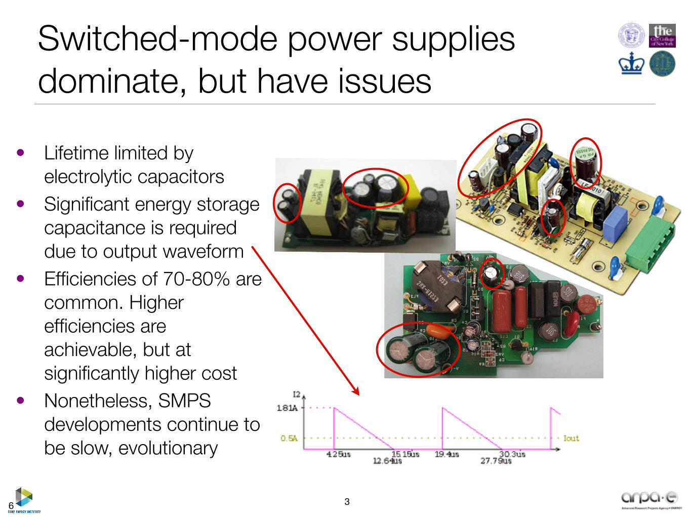
• Lifetime limited by electrolytic capacitors
• Significant energy storage capacitance is required due to output waveform
• Efficiencies of 70-80% are common. Higher efficiencies are achievable, but at significantly higher cost
• Nonetheless, SMPS developments continue to be slow, evolutionary
Switched-mode power supplies dominate, but have issues
6
RDR-195 14 W PAR38 LED Driver Using LNK406EG 13-May-11
Page 6 of 40
Power Integrations, Inc. Tel: +1 408 414 9200 Fax: +1 408 414 9201 www.powerint.com
Figure 1 – Populated Circuit Board Photograph (Top View). PCB Outline Designed to Fit Inside PAR38
Enclosure.
Figure 2 – Populated Circuit Board Photograph (Bottom View).
4
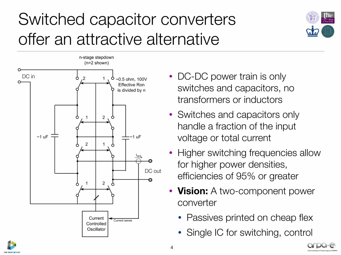
Switched capacitor converters offer an attractive alternative
• DC-DC power train is only switches and capacitors, no transformers or inductors
• Switches and capacitors only handle a fraction of the input voltage or total current
• Higher switching frequencies allow for higher power densities, efficiencies of 95% or greater
• Vision: A two-component power converter• Passives printed on cheap flex• Single IC for switching, control
8
ARPA-E Cooperative Agreement DE-AR0000114 With City University of New York (CUNY) Energy Institute (EI)
9
development now in process. In the middle is a DC bus or link, with voltage in the range of 170-200 V, for a 110 VRMS AC line. (This voltage would be about double for a 220 VRMS AC line.) The figure includes a bulk capacitor that would be needed to provide energy balance if the LEDs are to be driven without a double-line-frequency (eg. 120 Hz) ripple component. We remain open to the possibility that standards may evolve to allow such double-line-frequency ripple to be applied to the LEDs, and would like to take advantage of this as an opportunity to allow reduction of the required energy storage. The diagram of Figure 8 has dotted lines indicating that this bulk capacitor, if used, might not be connected directly to the DC bus. However, we are gravitating toward placing the main energy storage capacitance directly on the DC bus. During Q2, our team has made considerable progress on two candidate LED driver circuit designs to interface the intermediate DC bus to a single LED string. Both are based on switched-capacitor type topologies. One includes galvanic isolation, accomplished by a capacitive interface, while the second does not include galvanic isolation. As discussed, for the second circuit design, galvanic safety isolation between the LED string and the heat spreader/sink will be needed. Details on these two circuit approaches comprise the rest of this section.
Figure 9. Capacitively isolated hybrid switched-capacitor resonant topology. Capacitively isolated hybrid switched-capacitor resonant LED driver circuit Figure 9 conceptually illustrates a capacitively isolated hybrid switched-capacitor resonant circuit that is fed by the rectified DC link voltage from Figure 8, and is designed to drive a string of LEDs. As a conceptual circuit, the left side comprises a double-ended switched capacitor ladder circuit. The illustration of Figure 9 shows a two-stage ladder, allowing a step down in voltage by two. This should be thought of as generalizable to many stages of step down to allow convenient matching between the DC line voltage and the nominal LED string voltage. A prototype to be discussed here actually utilizes a three-stage ladder. The second stage of this hybrid circuit is a standard series resonant stage. This is also double-ended, as illustrated in Figure 9. This double-ended approach is natural since it is the pair of capacitors in the resonant stage that effects galvanic isolation. Each of these two resonant capacitors must be rated to provide the required isolation voltage, i.e. 3 kV. The utilization of the ladder step down stage enables the series resonant converter stage to operate at or near its maximum efficiency. This is the case since the series resonant stage then only needs to step down
DC in
DC out
5
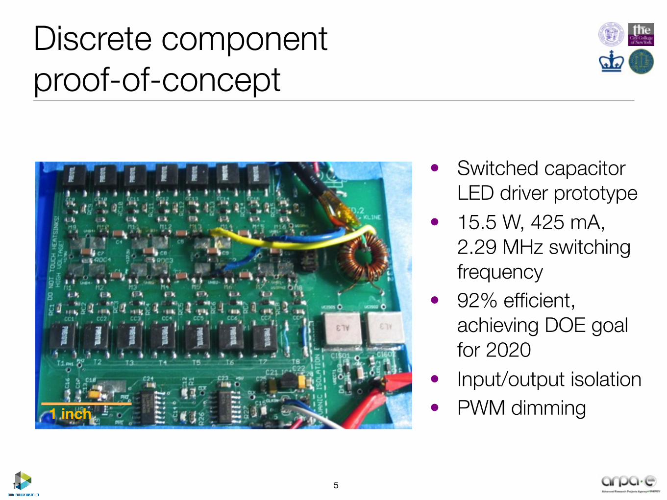
Discrete component proof-of-concept
• Switched capacitor LED driver prototype
• 15.5 W, 425 mA, 2.29 MHz switching frequency
• 92% efficient, achieving DOE goal for 2020
• Input/output isolation • PWM dimming1 inch
11
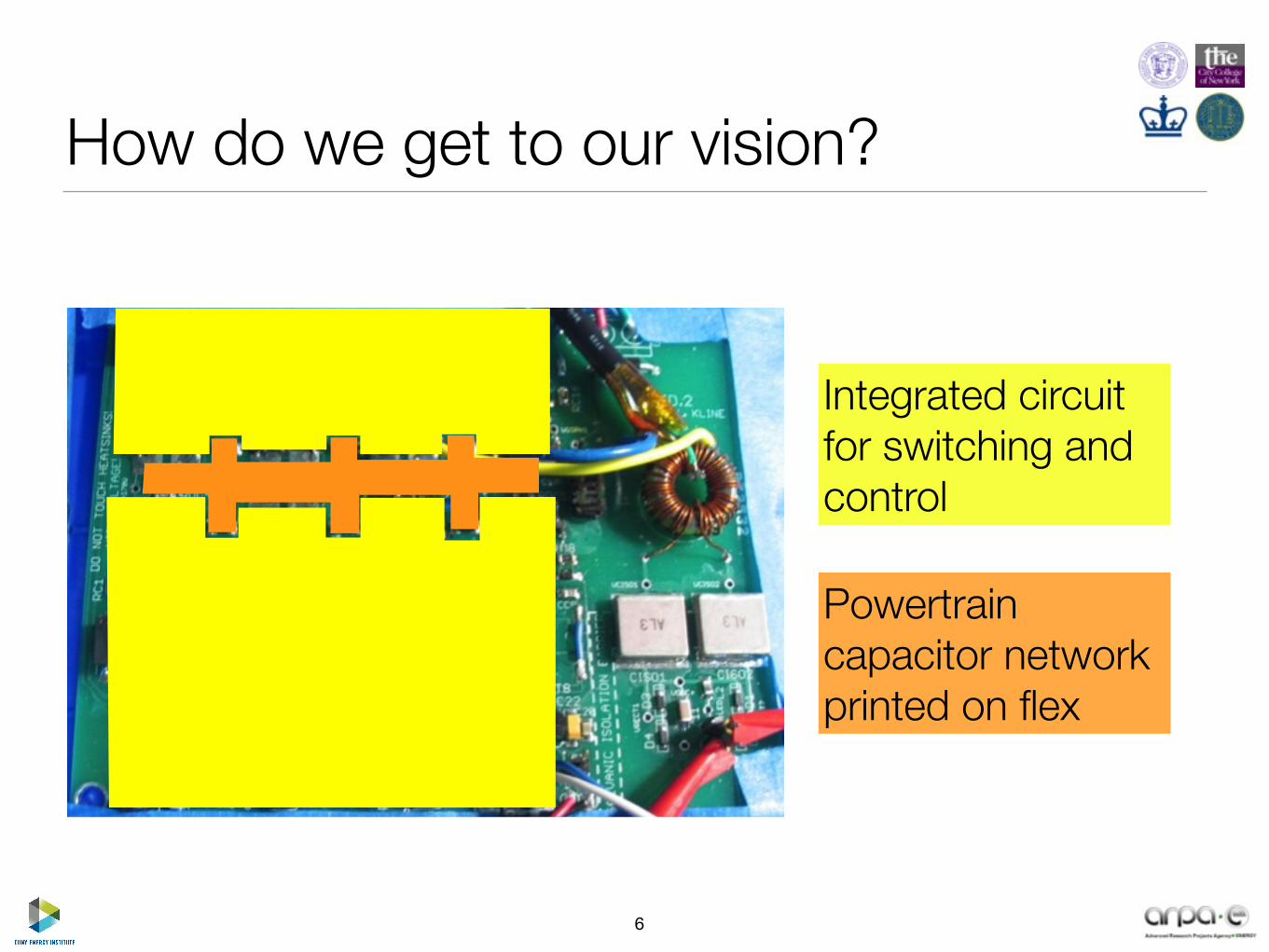
Integrated circuit for switching and control
Powertrain capacitor network printed on flex
6
How do we get to our vision?
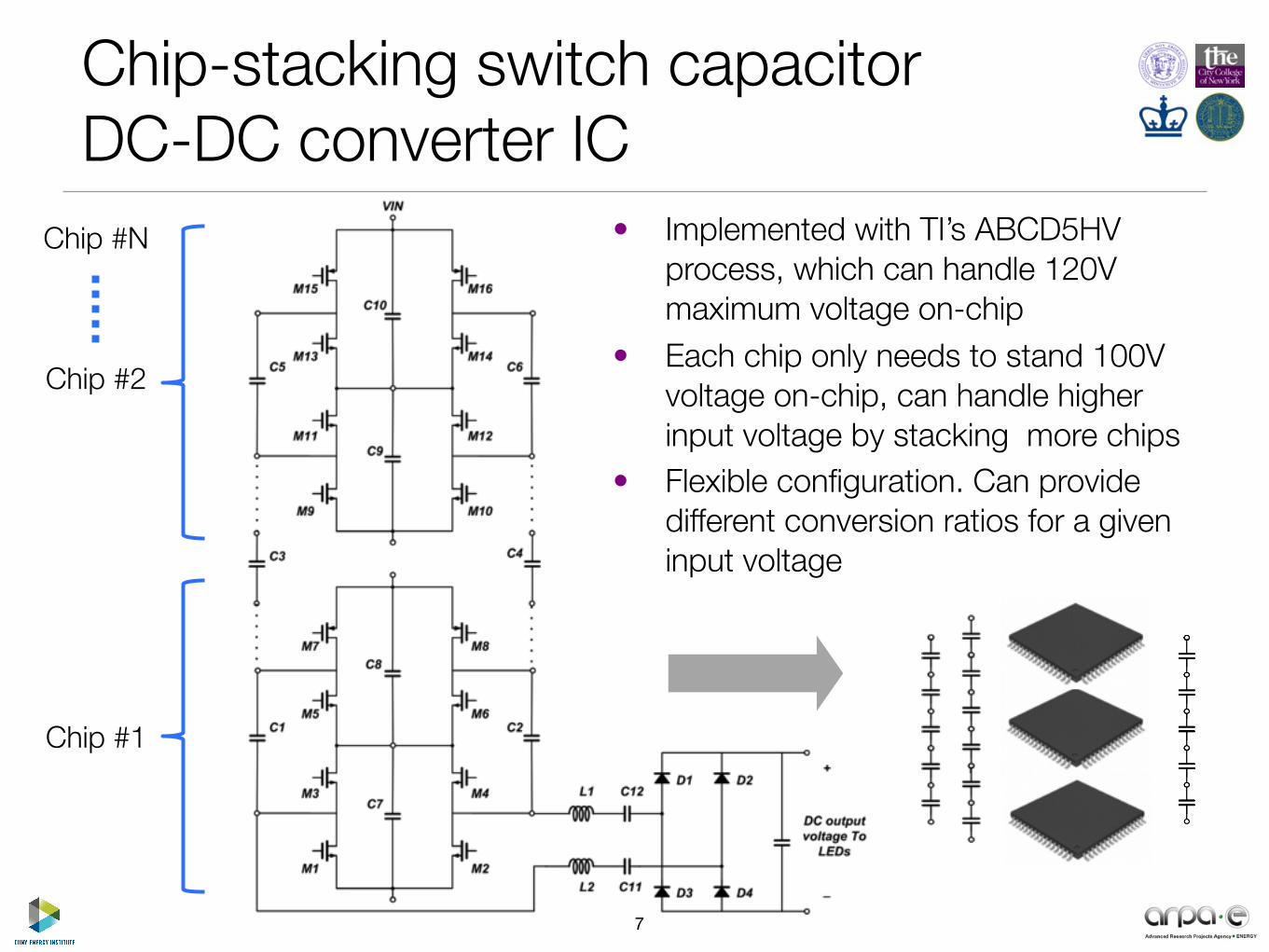
Chip-stacking switch capacitorDC-DC converter IC
Chip #1
Chip #2
Chip #N
7
• Implemented with TI’s ABCD5HV process, which can handle 120V maximum voltage on-chip
• Each chip only needs to stand 100V voltage on-chip, can handle higher input voltage by stacking more chips
• Flexible configuration. Can provide different conversion ratios for a given input voltage

Multi-level PFC rectifier Switched-Capacitor Regulator
Discrete PFC off-line LED driver prototype
8
What about the capacitors?
• High-frequency• Cheap!
• Printable • Roll-to-roll process compatible• Low-temperature fabrication
9

Printable nanoparticle dielectric
• BaTiO3 and (Ba, Sr)TiO3 nanoparticles, single crystal, size controllable from 5-100 nm
• Low temperature (<100°C), scalable batch synthesis; no HTCC/LTCC processing
• Size, composition determined by solvents (alcohol, water) and metal-organic precursors
10
FULL
PAPER
respect tomanysubstrates andare a red light forany possibility of adoption by semiconductorindustry integrated device manufacturers(IDMs). Furthermore, future technologies thatmay rely heavily on organic components(plastic electronics, printed or flexible electro-nics, organic FETs) are seeking thin films ofsuitable dielectric strength that can be incorpo-rated into entirely solution-based or low-temperature processing, such as ink-jetprinting, and can withstand some reasonablelevel of deformation.[19,20] The emerging fieldof nanodielectrics (also called nanometricdielectrics), which specifically deals with thescaling of both ceramic and matrix into thenanoregime,[21–23] impacts research and devel-opment from tunable insulators to advancedmaterials for energy storage.[6,24–26]
2. Results and Discussion
Aggregate-free, highly crystalline, and uniformnanocrystals with narrow size distributions,good size tunability/dispersibility in solventsare strong candidates for solving issuesassociated with device integration with eitherconventional semiconductor fabrication orpolymer-based organic electronics. Throughsystematic study as a function of size, they alsofurther the means to understand the underlying physicalphenomenon that govern properties at the nanoscale, and aid inthe development of a roadmap for future device architectures thatwill be partially or fully constructed from techniques that fall undertheumbrella of self-assembly. In the case of barium titanate, awidevariety of synthesis approaches to nanostructures (nanocrystals,nanowires and nanotubes) have been reported.[14,27–35] Sincemostnonaqueous processes take place at high temperatures (200–350 8C), high-boiling-point solvents (e.g., long-chain hydrocar-bons, diphenyl ether, trioctylamine, or oleylamine) are commonlyused as reaction media. And surface capping agents (e.g.,trioctylphosphine oxide, oleic acid) are introduced to controlcrystal growth and stabilize the nanostructures by providingsurface coatings.[35–38] We set out to eliminate the need for ligandcontrol while maintaining quality of the final product, usingalcohols such as ethanol and isopropanol as a solvent, BaTi metal-organic sources as a BaTiO3 precursor, and adapting provensolvothermal methods.[34,39] Controlled amounts of water arefound to improve crystal solubility and size tunability withoutcompromising crystallinity. The process enables the production ofuniform, aggregate-free and highly crystalline BaTiO3 or(Ba,Sr)TiO3 nanocrystals with high yields (>90%) and tunablesizes ranging from about 5 to 100 nm, mainly depending on thetype of BaTimetal-organic sources and the type of alcohols used inthe synthesis. Further details on the synthesis and mechanismswill be reported in a separate paper.
BaTiO3 and (Ba,Sr)TiO3 (BST) nanocrystals were preparedby reacting 95% ethanol with two different metal-organicsources, barium titanium ethylhexano-isopropoxide, and barium,
strontium and titanium isopropoxide, respectively. Transmissionelectron microscopy (TEM; Fig. 1a,b) confirms that the samplesconsist of discrete BaTiO3 nanocrystals with a relatively narrowsize distribution. Nanocrystals of this size have previously beenidentified as predominantly single crystal, below a natural limit fordomain formation. Figure 1c,d present typical X-ray diffraction(XRD) patterns of the samples prepared using different bariumtitanium metal-organic sources. All diffraction peaks can beassigned to the perovskite BaTiO3 phase (Joint Committee onPowder Diffraction Standards—JCPDS No. 31–174) or(Ba,Sr)TiO3 phasewithout any indication of crystalline byproductssuch as BaCO3 or TiO2. The measurement indicates the exclusivepresence of the perovskite phases in high crystallinity and purity.The sizes of the nanocrystals vary when prepared using differentalcohol solvents and different metal-organic sources, as indicatedby the extent of the diffraction peak broadening (Fig. 1c,d), and areconsistent with the results based on the TEM observations(Fig. 1a,b). It is found that controlled amountsofwater can improvecrystal size tunability without compromising crystallinity(Supporting Information, s-Table 1.).
The solvothermal process involves alcoholysis between twosimple sources: a metal-organic precursor and an alcohol. Noorganic surfactant, high boiling point solvent, alkaline or halideresources are included. The method produces highly pure, highlycrystalline BaTiO3 nanocrystals with minimal organic residuals,and it is free from contamination of alkali/halide ions. Moreover,BT and BST nanocrystals synthesized in 95% ethanol andalcohol with controlled amounts of water show high dispersibilityand stability in polar solvents (such as ethanol and
www.MaterialsViews.comwww.afm-journal.de
Figure 1. TEM images of BaTiO3 nanocrystals synthesized based on a solvothermal processbetween 95% ethanol and a barium titanium metal-organic source such as a) barium titaniumethylhexano-isopropoxide and b) barium and titanium isopropoxide; c) XRD patterns of BaTiO3
and Ba0.5Sr0.5TiO3 nanocrystals of 25 nm in diameter; d) XRD patterns of BaTiO3 andBa0.7Sr0.3TiO3 nanocrystals of 10 nm in diameter.
Adv. Funct. Mater. 2010, 20, 554–560 ! 2010 WILEY-VCH Verlag GmbH & Co. KGaA, Weinheim 555
O'Brien, S., Huang, L. & Chen, Z. METAL OXIDE NANOCRYSTALS: PREPARATION AND USES. USA patent application 12/566,135
5 nm
100 nm 100 nm
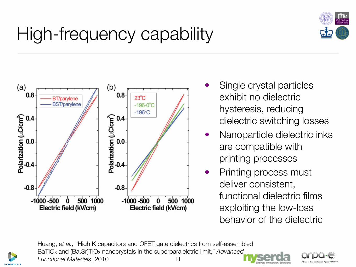
High-frequency capability
• Single crystal particles exhibit no dielectric hysteresis, reducing dielectric switching losses
• Nanoparticle dielectric inks are compatible with printing processes
• Printing process must deliver consistent, functional dielectric films exploiting the low-loss behavior of the dielectric
FULL
PAPER
constant increases from 47 to 58 (measured at 100 kHz) by fillingthe voidswith amorphousBTmaterials followedby 60 8Cbaking inair. The dielectric loss remains stable and at a low level under N2
(tan d! 0.04–0.05).Reported loss values of thickBTfilmspreparedby sintering, spark plasma sintering, or radio frequency (r.f.)sputtering, are in the range of 0.01–0.06.[18,40,41] Commerciallyavailable electrolytic capacitors measured on the same apparatuspossess losses in the range of 0.04–0.09 (0.1–1mF). When BT(BaTiO3) nanocrystals (25 nm) are uniformly incorporated intopoly(a-methylstyrene) (1:1 weight ratio), the dielectric constantsshow significant increase from !2.5 for the pure polymer to !18for the nanocomposite thin film, and remain stable in thefrequency range of 100Hz to 1MHz.
The critical size limit for free standing (3D) particles hasbeen hotly debated, aided by a range of techniques andprobes.[4,5,13,15,38,42] Suppression of ferroelectricity in free stand-ing particles has been predicted and observed in PbTiO3 andBaTiO3 among others.[38] Here we show that BTand BSTparticlesof up to 12 nm in size remain superparaelectric when assembledinto films, noting that no grain growth is observed or expected atprocessing at 60 8C. We observe paraelectric behavior over atemperature range of "196 to 24 8C through the distinctobservation of no hysteresis in a series of polarization versuselectric field measurements (Fig. 4). The lack of a phase transition(between cubic and tetragonal phases) between 22 and 220 8C asobserved in Raman spectra (Supporting Information) suggests
stable and less temperature dependant dielectric constants over awide temperature range, which would be beneficial for capacitorand gate dielectric applications. Moreover, the high dielectricconstant and lack of hysteresis loop in the polarization–electricfield plot for the BaTiO3 nanocrystal thin film also show a potentialapplication of the thin film as a high k gate dielectric for OFETs.
OFETs are potentially competent components for large-areaelectronics[43–45] because of their attractive advantages: lightweight, cost-effective and large-area processability, flexibility,and prospective performance potential. Great effort has beenmade to overcome the obstacles for commercial applications ofOFETs, such as low mobility (low current capacity) and very highoperation voltage[46] (limited subthreshold slope). One likely wayto overcome both problems is to use high-capacitance gatedielectrics, which can lower the operation voltage and increasethe filled accumulated carrier density, thus increasing themobilityby filling the energy traps inOFETs.[46–56] Themethod of using thenanoparticle–polymer composite gate dielectrics[57–61] appears tohave all the advantages simultaneously: much higher dielectricconstant compared to polymer dielectrics, low-temperature andlarge-area processing, and low cost of materials and fabrication,although some of the composites undergo polarization hyster-esis[57,59] and the dielectric constant is limited by the low kpolymerand finite solubility of nanocrystals in polymer solution.
We fabricated pentacene OFETs with spin-cast high-k bariumtitanate nanoparticle thin films as the gate dielectric on glass andflexible PEN substrates (Fig. 5). In order to solve the incompat-ibility between inorganic BT (or BST) gate dielectric and theorganic semiconductor active layer, a thin layer of parylene-C isevaporated in our customized chemical vapor deposition (CVD)system. The whole fabrication process is operated below 60 8C.Parylene coating not only helps decrease the surface roughness ofnanocrystal thin film, but also provides a favorable surface for thegrowth of high-quality pentacene. Figure 5 is a comparison of thepentacene grown on bare BT thin film and BT–parylene-C thinfilm. The pentacene grains fail to form a continuous film on bareBaTiO3 and exhibit a large fraction of vertical grains. No
www.MaterialsViews.comwww.afm-journal.de
Figure 3. Frequency dependence of dielectric constant and dielectric lossfor a) BST and b) BT nanocrystal thin films assembled with 8 nm diameternanocrystals at room temperature.
Table 1. Dielectric constant of self-assembled nanocrystal thin films as afunction of crystal size (film thickness: 200–300 nm).
Thin film sample Crystal size
[nm]
Dielectric constant
(measured at 100 kHz)
BaTiO3 8–12 22–25
25–30 34
BaTiO3/parylene 8–12 10
25–30 13
Ba0.7Sr0.3TiO3 8–12 27
25–30 47
Ba0.7Sr0.3TiO3/parylene 8–12 12
25–30 16
Figure 4. Ferroelectric measurements of assembled nanocrystal thinfilms of BT and BST in Sawyer–Tower configuration under conditions ofa) demoisturized films with an evaporated film of parylene, dried at 60 8Cand b) RT and immersed in liquid N2 for the BT/parylene thin film.
Adv. Funct. Mater. 2010, 20, 554–560 ! 2010 WILEY-VCH Verlag GmbH & Co. KGaA, Weinheim 557
Huang, et al., “High K capacitors and OFET gate dielectrics from self-assembled BaTiO3 and (Ba,Sr)TiO3 nanocrystals in the superparalelctric limit,” Advanced Functional Materials, 2010 11
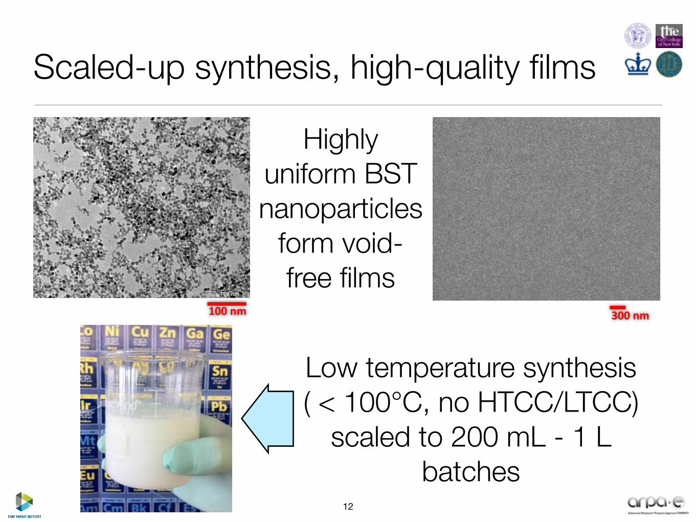
Scaled-up synthesis, high-quality films
12
5 ARPA-E Cooperative Agreement DE-AR0000114 With City University of New York (CUNY) Energy Institute (EI)
Figure 2. (left) snapshots of a beaker containing about 200 ml nanocrystal suspension (~25 nm in diameter, ethanol as solvent, 20 mg/ml).(right). (right) SEM image of BST nanocrystals. Table 1. Scale-up synthesis (200ml-1L) of BT/BST nanocrystals and their size distribution.
Method Synthesis condition Crystal Size (nm)
Standard Deviation (%)
Reflux method
(78oC x 3-8hrs)
Ba(iPr)2+Sr(iPr)2+Ti(iPr)4 + ethanol/H2O BaTi ethylhexano-isoproxide+ethanol/H2O
H2O: 5 vol% H2O: 25 vol% H2O: 50 vol% H2O: 5 vol%
11.0 20.3 46.1
30.0
6.6 5.6 6.5
6.8
Ba(ac)2+Sr(ac)2+Ti(iPr)4 or Ti(Bu)4+ ethanol/H2O + OH
OH/Ti(Bu)4=4 OH/Ti(iPr)4=4 OH/Ti(iPr)4=40
17.7 25.2 41.9
7.0 10.8 10.9
Low T solvothermal treatment (45-55oC x 5-20hrs)
Ba(iPr)2+Sr(iPr)2+Ti(iPr)4 + ethanol/H2O
H2O: 2.5 vol% H2O: 5 vol%
7.1 9.6
6.5 6.0
(3) Ultimate low temperature solvothermal process (45-55oC) We are further testing the potential ability to reduce the crystallization temperature of BaSrTi isopropoxide precursors in ethanol, which we have observed can be further reduced to 45-55oC while still maintaining high crystallinity, high purity and good dispersibility of BST nanocrystal products (Figure 3). The crystal size is dependant to the water content in the system but is insensitive to the crystallization temperature and time when water content is constant. The lower synthesis temperature and thus near atmosphere pressure (1.3 atm) can offer great benefits for scale-up synthesis. It can further reduce operation costs since no stirring is necessary, and the reaction can simply take place in a regular polypropylene bottle. The as-synthesized nanocrystal solution was analyzed with UV-vis spectra, which show absorption peaks at 232 nm (Figure 4). According to the standard curve of absorption vs. concentration reported in Q2 report, the concentrations of the as-synthesized nanocrystals at different crystallization time were calculated accordingly. It shows that the nanocrystals can reach more than 90% yield after 5 hrs and get fully crystallized after 10 hrs.
ADEPTMetacapacitors,DE‐AR0000114
Confiden;alFilesAllrightsreservedPage2
GeneralizedProduct
Method Synthesis condition Crystal Size
(nm)
Standard
Deviation (%)
Reflux method
(78oC x 3-8hrs)
Ba(iPr)2+Sr(iPr)2+Ti(iPr)4
+ ethanol/H2O
BaTi ethylhexano-
isoproxide+ethanol/H2O
H2O: 5 vol%
H2O: 25 vol%
H2O: 50 vol%
H2O: 5 vol%
11.0
20.3
46.1
30.0
6.6
5.6
6.5
6.8
Ba(ac)2+Sr(ac)2+Ti(iPr)4
or Ti(Bu)4+ ethanol/H2O
+ OH
OH/Ti(Bu)4=4
OH/Ti(iPr)4=4
OH/
Ti(iPr)4=40
17.7
25.2
41.9
7.0
10.8
10.9
Low T solvothermal
treatment
(45-55oC x 5-20hrs)
Ba(iPr)2+Sr(iPr)2+Ti(iPr)4
+ ethanol/H2O
H2O: 2.5 vol
%
H2O: 5 vol%
7.1
9.6
6.5
6.0
Figure 5. (left) SEM image of a BST nanocrystal thin film spin-coated with the as-synthesized
nanocrystal solution; (right) TEM image of as-synthesized BST nanocrystals (~7 nm). ADEPTMetacapacitors,DE‐AR0000114
Confiden;alFilesAllrightsreservedPage2
GeneralizedProduct
Method Synthesis condition Crystal Size
(nm)
Standard
Deviation (%)
Reflux method
(78oC x 3-8hrs)
Ba(iPr)2+Sr(iPr)2+Ti(iPr)4
+ ethanol/H2O
BaTi ethylhexano-
isoproxide+ethanol/H2O
H2O: 5 vol%
H2O: 25 vol%
H2O: 50 vol%
H2O: 5 vol%
11.0
20.3
46.1
30.0
6.6
5.6
6.5
6.8
Ba(ac)2+Sr(ac)2+Ti(iPr)4
or Ti(Bu)4+ ethanol/H2O
+ OH
OH/Ti(Bu)4=4
OH/Ti(iPr)4=4
OH/
Ti(iPr)4=40
17.7
25.2
41.9
7.0
10.8
10.9
Low T solvothermal
treatment
(45-55oC x 5-20hrs)
Ba(iPr)2+Sr(iPr)2+Ti(iPr)4
+ ethanol/H2O
H2O: 2.5 vol
%
H2O: 5 vol%
7.1
9.6
6.5
6.0
Figure 5. (left) SEM image of a BST nanocrystal thin film spin-coated with the as-synthesized
nanocrystal solution; (right) TEM image of as-synthesized BST nanocrystals (~7 nm).
100 nm 300 nm
Low temperature synthesis ( < 100°C, no HTCC/LTCC)
scaled to 200 mL - 1 L batches
Highly uniform BST nanoparticles
form void-free films

Early prototypes: Spin-coated BST with parylene capping layer
FULL
PAPER
constant increases from 47 to 58 (measured at 100 kHz) by fillingthe voidswith amorphousBTmaterials followedby 60 8Cbaking inair. The dielectric loss remains stable and at a low level under N2
(tan d! 0.04–0.05).Reported loss values of thickBTfilmspreparedby sintering, spark plasma sintering, or radio frequency (r.f.)sputtering, are in the range of 0.01–0.06.[18,40,41] Commerciallyavailable electrolytic capacitors measured on the same apparatuspossess losses in the range of 0.04–0.09 (0.1–1mF). When BT(BaTiO3) nanocrystals (25 nm) are uniformly incorporated intopoly(a-methylstyrene) (1:1 weight ratio), the dielectric constantsshow significant increase from !2.5 for the pure polymer to !18for the nanocomposite thin film, and remain stable in thefrequency range of 100Hz to 1MHz.
The critical size limit for free standing (3D) particles hasbeen hotly debated, aided by a range of techniques andprobes.[4,5,13,15,38,42] Suppression of ferroelectricity in free stand-ing particles has been predicted and observed in PbTiO3 andBaTiO3 among others.[38] Here we show that BTand BSTparticlesof up to 12 nm in size remain superparaelectric when assembledinto films, noting that no grain growth is observed or expected atprocessing at 60 8C. We observe paraelectric behavior over atemperature range of "196 to 24 8C through the distinctobservation of no hysteresis in a series of polarization versuselectric field measurements (Fig. 4). The lack of a phase transition(between cubic and tetragonal phases) between 22 and 220 8C asobserved in Raman spectra (Supporting Information) suggests
stable and less temperature dependant dielectric constants over awide temperature range, which would be beneficial for capacitorand gate dielectric applications. Moreover, the high dielectricconstant and lack of hysteresis loop in the polarization–electricfield plot for the BaTiO3 nanocrystal thin film also show a potentialapplication of the thin film as a high k gate dielectric for OFETs.
OFETs are potentially competent components for large-areaelectronics[43–45] because of their attractive advantages: lightweight, cost-effective and large-area processability, flexibility,and prospective performance potential. Great effort has beenmade to overcome the obstacles for commercial applications ofOFETs, such as low mobility (low current capacity) and very highoperation voltage[46] (limited subthreshold slope). One likely wayto overcome both problems is to use high-capacitance gatedielectrics, which can lower the operation voltage and increasethe filled accumulated carrier density, thus increasing themobilityby filling the energy traps inOFETs.[46–56] Themethod of using thenanoparticle–polymer composite gate dielectrics[57–61] appears tohave all the advantages simultaneously: much higher dielectricconstant compared to polymer dielectrics, low-temperature andlarge-area processing, and low cost of materials and fabrication,although some of the composites undergo polarization hyster-esis[57,59] and the dielectric constant is limited by the low kpolymerand finite solubility of nanocrystals in polymer solution.
We fabricated pentacene OFETs with spin-cast high-k bariumtitanate nanoparticle thin films as the gate dielectric on glass andflexible PEN substrates (Fig. 5). In order to solve the incompat-ibility between inorganic BT (or BST) gate dielectric and theorganic semiconductor active layer, a thin layer of parylene-C isevaporated in our customized chemical vapor deposition (CVD)system. The whole fabrication process is operated below 60 8C.Parylene coating not only helps decrease the surface roughness ofnanocrystal thin film, but also provides a favorable surface for thegrowth of high-quality pentacene. Figure 5 is a comparison of thepentacene grown on bare BT thin film and BT–parylene-C thinfilm. The pentacene grains fail to form a continuous film on bareBaTiO3 and exhibit a large fraction of vertical grains. No
www.MaterialsViews.comwww.afm-journal.de
Figure 3. Frequency dependence of dielectric constant and dielectric lossfor a) BST and b) BT nanocrystal thin films assembled with 8 nm diameternanocrystals at room temperature.
Table 1. Dielectric constant of self-assembled nanocrystal thin films as afunction of crystal size (film thickness: 200–300 nm).
Thin film sample Crystal size
[nm]
Dielectric constant
(measured at 100 kHz)
BaTiO3 8–12 22–25
25–30 34
BaTiO3/parylene 8–12 10
25–30 13
Ba0.7Sr0.3TiO3 8–12 27
25–30 47
Ba0.7Sr0.3TiO3/parylene 8–12 12
25–30 16
Figure 4. Ferroelectric measurements of assembled nanocrystal thinfilms of BT and BST in Sawyer–Tower configuration under conditions ofa) demoisturized films with an evaporated film of parylene, dried at 60 8Cand b) RT and immersed in liquid N2 for the BT/parylene thin film.
Adv. Funct. Mater. 2010, 20, 554–560 ! 2010 WILEY-VCH Verlag GmbH & Co. KGaA, Weinheim 557
glass substrate
BST film
Au electrode parylene-c
200 nm
13
• Spin-coated nanoparticles on glass with thermally-evaporated Au electrodes• CVD Parylene-C layer to reduce high-frequency loss• Capacitance flat to 10 MHz, dissipation factor < 0.05 at 1 MHz• Not roll-to-roll compatible, difficult to scale vertically

Dielectric properties improve with printable polyfurfuryl alcohol (PFA) copolymer
BST8 thin film
With in-situ polymerization, nanocrystal surface passivated, defects or pinholes reduced, fewer
absorbents:
• stable and increased readings in capacitance;• low and stable readings in dielectric loss;• increase of k compared with that for pure BST:
indicating that FA and PFA penetrate into voids.
• Much higher capacitance and dielectric loss at low frequency (< 1kHz) due to leakage current
(carriers, defects, pinholes)
• Dramatic change in capacitance and dielectric loss with frequency due to different
contributions from space charges or water molecules at various frequencies.
BST8 with PFAFA treatment
k=~ 15 (1MHz) K=~17-19 (1MHz)
14
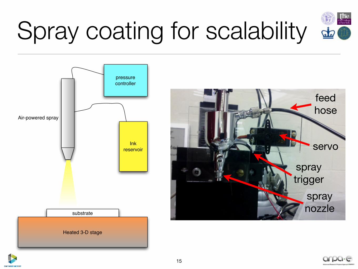
Spray coating for scalabilitypressure controller
substrate
Ink reservoir
Heated 3-D stage
Air-powered spray
15
servo
spray nozzle
spray trigger
feed hose

Spray coating process
1. Deposit evaporated aluminum electrode
2. Print dielectric layer3. Heat treatment4. Deposit next
electrode layer5. Repeat to build
multilayer structure
16
SubstrateElectrode
SubstrateElectrode
SubstrateElectrode
HOT
SubstrateElectrode
Electrode
1
3
2
4 5
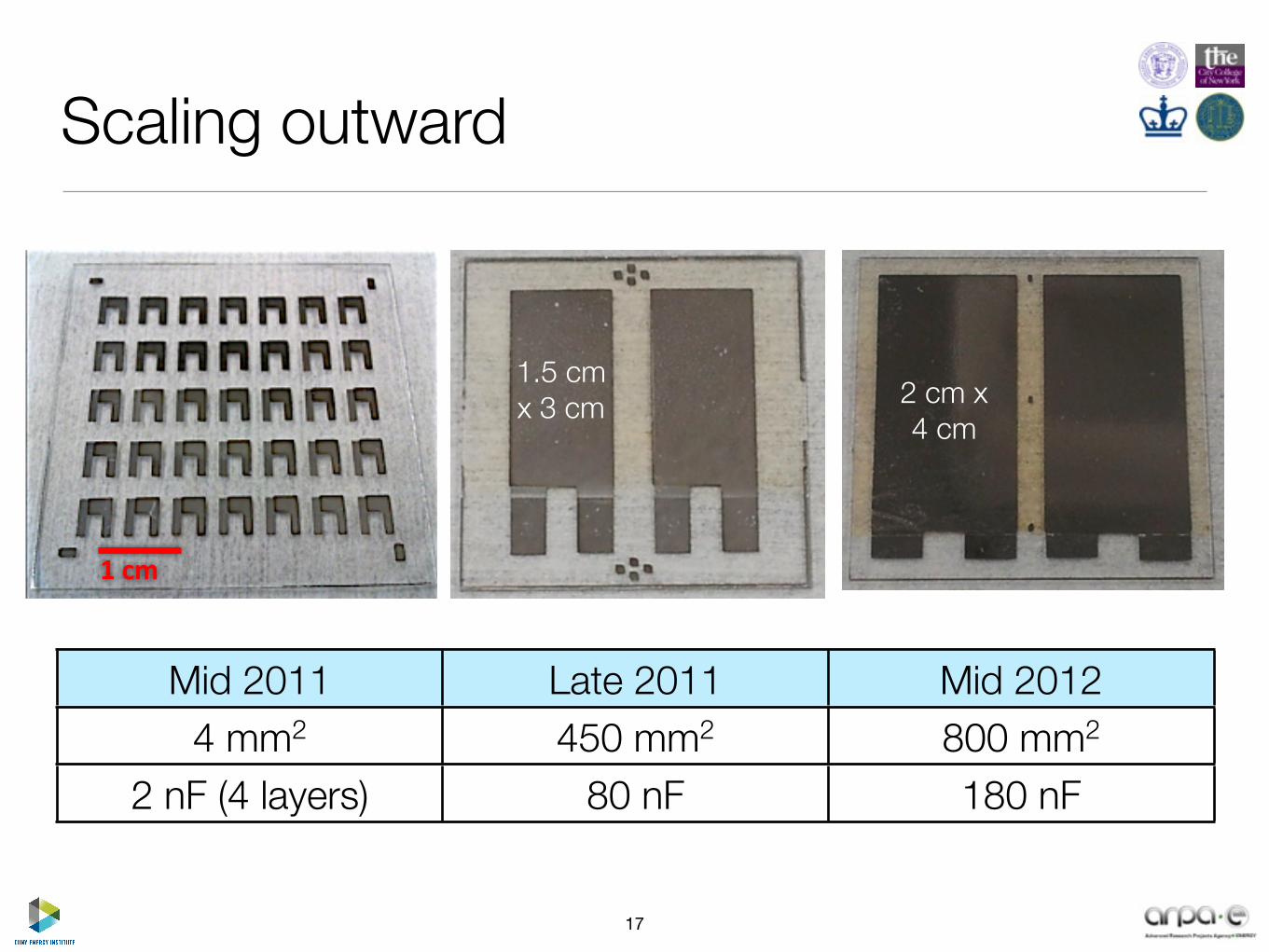
Scaling outward
17
1.5 cm x 3 cm 2 cm x
4 cm
1 cm
Mid 2011 Late 2011 Mid 20124 mm2 450 mm2 800 mm2
2 nF (4 layers) 80 nF 180 nF
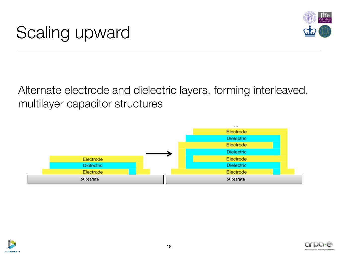
Alternate electrode and dielectric layers, forming interleaved, multilayer capacitor structures
Substrate Substrate
Scaling upward
18
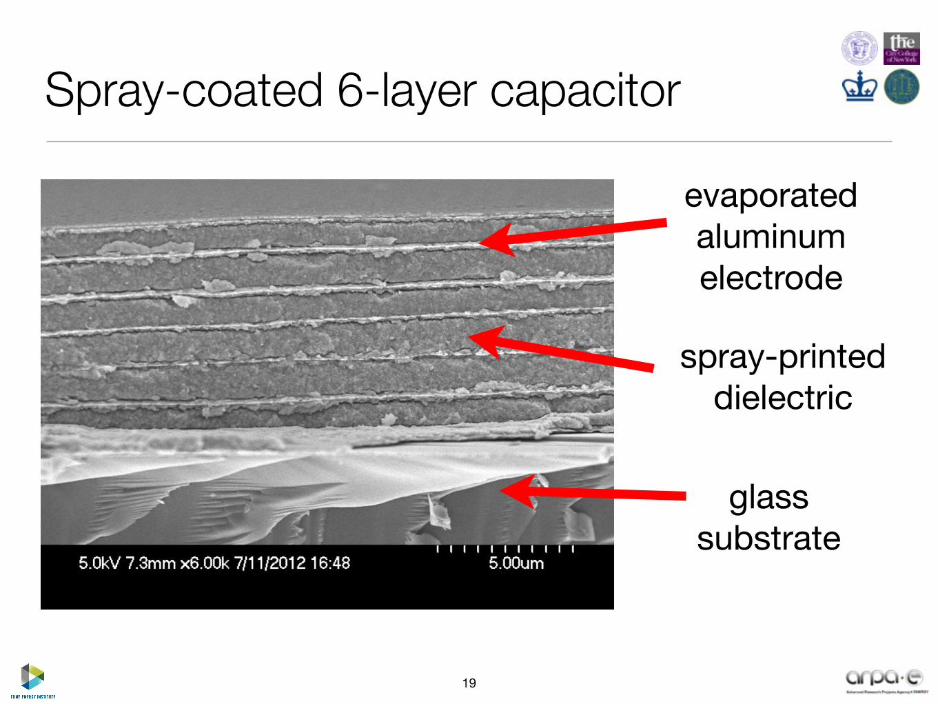
Spray-coated 6-layer capacitor
19
glass substrate
evaporated aluminum electrode
spray-printed dielectric

Wide-area dielectric films by spray printing
20
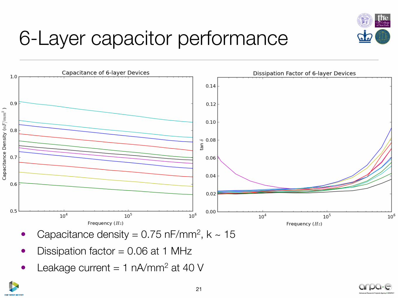
6-Layer capacitor performance
21
• Capacitance density = 0.75 nF/mm2, k ~ 15• Dissipation factor = 0.06 at 1 MHz• Leakage current = 1 nA/mm2 at 40 V

Increasing capacitance layer-by-layer
22
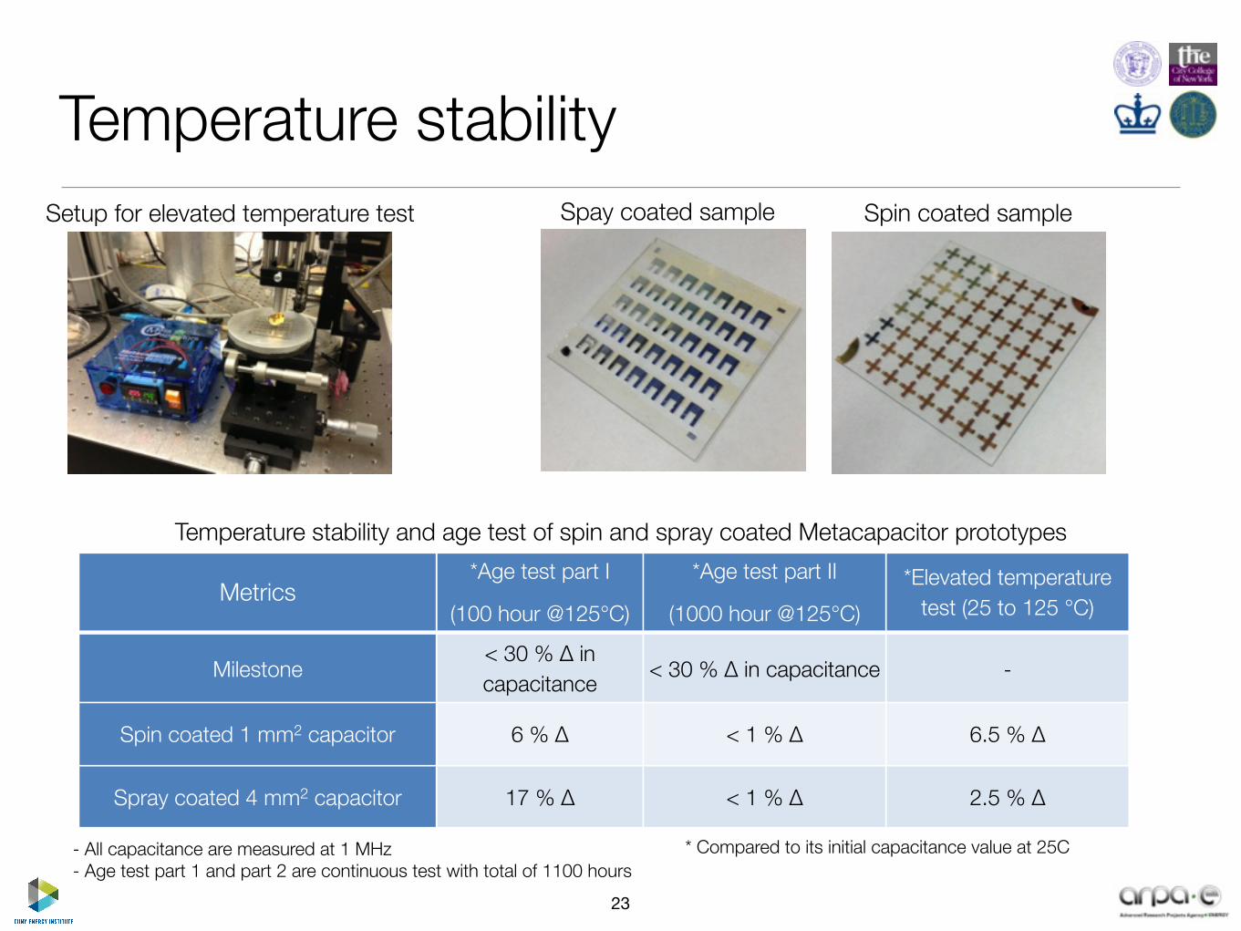
Temperature stability
23
Setup for elevated temperature test
Metrics*Age test part I
(100 hour @125°C)
*Age test part II
(1000 hour @125°C)*Elevated temperature
test (25 to 125 °C)
Milestone
Spin coated 1 mm2 capacitor
Spray coated 4 mm2 capacitor
< 30 % ∆ in capacitance < 30 % ∆ in capacitance -
6 % ∆ < 1 % ∆ 6.5 % ∆
17 % ∆ < 1 % ∆ 2.5 % ∆
Temperature stability and age test of spin and spray coated Metacapacitor prototypes
Spin coated sampleSpay coated sample
* Compared to its initial capacitance value at 25C - All capacitance are measured at 1 MHz - Age test part 1 and part 2 are continuous test with total of 1100 hours
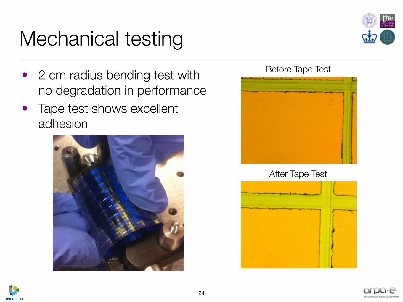
Mechanical testing• 2 cm radius bending test with
no degradation in performance• Tape test shows excellent
adhesion
24
Before Tape Test
After Tape Test

Integration to a power circuit
25
Metacapacitors in a 1 MHz LED driver regulator circuit
• Spray-coated caps on glass • Spin-coated caps on flex

Thanks!
26
Prof. Steve O’BrienChemistry
CCNY
Prof. Dan SteingartChemical engineering
CCNY
Prof. Ioannis KymissisElectrical engineering Columbia University
Prof. Alex CouzisChemical engineering
CCNY
Dr. Limin HuangChemistry
SCUST
Dr. Eli LelandChemical Engineering
CCNY
Shyuan YangElectrical EngineeringColumbia University
Barry Van TassellChemical engineering
CCNY
Paul ChandoChemical Engineering
CCNY
Contact: Eli Leland ([email protected])
Dr. Shuangyi LiuChemistry
CCNY
Prof. Peter KingetElectrical engineering Columbia University
Chengrui LeElectrical engineeringColumbia University
Prof. Seth SandersElectrical engineering
UC Berkeley
Daniel GerberElectrical engineering
UC Berkeley

backup
27

Moving forward
• Integrating spray-coating process on flexible substrates
• Testing custom power IC with printed capacitors
• Integrated LED driver prototype on flex!
28

Why capacitors instead of inductors?Type Manufacturer
Capacitance, Voltage rating
Dimensions(mm)
Energy density(µJ/mm3)
Ceramic Cap Taiyo-Yuden 22µF @4V 1.6 x 0.8 x 0.8 172
Ceramic Cap Taiyo-Yuden 1µF@35V 1.6 x 0.8 x 0.8 598
Tantalum Cap Vishay 10µF@4V 1.0 x 0.5 x 0.6 267
Tantalum Cap Vishay 100µ[email protected] 2.4 x 1.45 x 1.1 518
Electrolytic Cap Kemet 22µF@16V 7.3 x 4.3 x 1.9 47
Electrolytic Cap C.D.E 210mF@50V 76φ x 219 264
Shielded SMT Inductor Coilcraft 10µH @ 0.21A 2.6 x 2.1 x 1.8 0.022
Shielded SMT Inductor Coilcraft 100µH @ 0.1A 3.4 x 3.0 x 2.0 0.025
Shielded inductor Coilcraft 170µH @ 1.0A 11 x 11 x 9.5 0.074
Shielded inductor Murata 1 mH @ 2.4A 29.8φ x 21.8 0.189
>1000x
Capacitors have >1000x higher energy density than inductors for power handling applications
29

Metacapacitors™High-level LED driver architecture
• Output regulation is accomplished using frequency modulation of switching converter
30
28 ARPA-E Cooperative Agreement DE-AR0000114 With City University of New York (CUNY) Energy Institute (EI)
Figure 36. Overall architecture of the proposed LED driver. Blocks in the dash-line box will be integrated on chip.
The Analog Bipolar-CMOS-DMOS (ABCD) 5HV process from National Semiconductor is chosen for the integrated implementation. Some of the required power IC components and specifications for our LED driver are listed in Table 5. The maximum voltage rating for the ABCD5HV technology is 105 V. The process also provides different devices with rating voltages 7 V, 20 V, and 70 V. Various on chip resistances and zener diodes are also available. According to Table 5, ABCD5HV is sufficient for our design. The process design kit (PDK) of ABCD5HV has been set up in Columbia CISL lab and simulations have started. Table 5. Specification of ABCD5HV devices for integrated LED driver circuit.
Component ABCD5HV Supported
Devices
Rating Voltage
Description Discrete
Component Description
Switch in ladder circuit
NLDMOSAV VDS = 70 V VGS = 14 V
• RDS,ON•A = 119 mΩ.mm2 (VGS=14V, VDS=0.1V)
• VTH = 1.5V • For 0.5 RDS, ON, area =
0.24 mm2
60 V, 0.5 Ω
Rectifier diode DHV 100 V Substrate current alpha = 0.05 Schottky, 60 V, 1 A, 38 pF
CMOS NMOSLV, PMOSLV
VDS = 7 V VGS = 14 V
Can be used in control circuit -
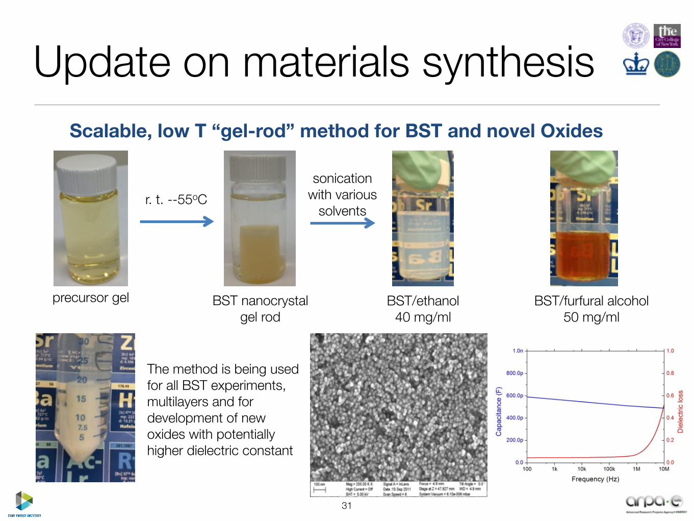
Update on materials synthesis
31
precursor gel BST nanocrystal gel rod
BST/furfural alcohol 50 mg/ml
BST/ethanol 40 mg/ml
sonication with various
solventsr. t. --55oC
Scalable, low T “gel-rod” method for BST and novel Oxides
The method is being used for all BST experiments, multilayers and for development of new oxides with potentially higher dielectric constant