metal nanoparticles for light trapping applications
DESCRIPTION
Plasmonic light trapping by metal nanoparticles has been considered as a mechanism toenhance light absorption by thin film silicon solar cells. We have studied the plasmonic interaction of lightwith silver nanoparticles. Using Mie theory, we first simulated the interaction of light with isolated silvernanoparticles in a continuous medium and studied the interaction as a function of particle size and thesurrounding medium. We calculated the absorption, scattering and extinction cross-sections of the particles,and studied the dependence of these parameters as a function of particle size. We also created 3D modelsusing COMSOL and performed FEM simulations to study the interaction of light with silver nanoparticles andquantify the absorption, scattering and extinction cross-sections directly from the model. We aim to move onto the case where we have an array of interacting nanoparticles at the interface between two media, which isthe actual case in a plasmon enhanced solar cell, so that we can work on optimization of plasmonic lighttrapping for more efficient photovoltaic devices.TRANSCRIPT
2010PH10869; 2010PH10845 - 1
Metal Nanoparticles for Light Trapping Applications
Shubham Bansal (2010PH10869); Himanshu (2010PH10845)
Supervisors: Dr. Vamsi Krishna Komarala / Dr. Rajendra Singh
Abstract: Plasmonic light trapping by metal nanoparticles has been considered as a mechanism to enhance light absorption by thin film silicon solar cells. We have studied the plasmonic interaction of light with silver nanoparticles. Using Mie theory, we first simulated the interaction of light with isolated silver nanoparticles in a continuous medium and studied the interaction as a function of particle size and the surrounding medium. We calculated the absorption, scattering and extinction cross-sections of the particles, and studied the dependence of these parameters as a function of particle size. We also created 3D models using COMSOL and performed FEM simulations to study the interaction of light with silver nanoparticles and quantify the absorption, scattering and extinction cross-sections directly from the model. We aim to move on to the case where we have an array of interacting nanoparticles at the interface between two media, which is the actual case in a plasmon enhanced solar cell, so that we can work on optimization of plasmonic light trapping for more efficient photovoltaic devices.
Email: [email protected]; [email protected]
Major Project Part 1 (EPD 411)
INTRODUCTION
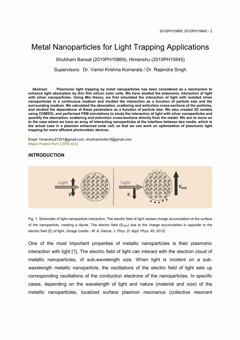
Fig. 1. Schematic of light-nanoparticle interaction. The electric field of light causes charge accumulation at the surface
of the nanoparticle, creating a dipole. The electric field (ERES) due to the charge accumulation is opposite to the
electric field (E) of light. (Image credits - M. A. Garcia, J. Phys. D: Appl. Phys. 45, 2012)
One of the most important properties of metallic nanoparticles is their plasmonic
interaction with light [1]. The electric field of light can interact with the electron cloud of
metallic nanoparticles, of sub-wavelength size. When light is incident on a sub-
wavelength metallic nanoparticle, the oscillations of the electric field of light sets up
corresponding oscillations of the conduction electrons of the nanoparticles. In specific
cases, depending on the wavelength of light and nature (material and size) of the
metallic nanoparticles, localized surface plasmon resonance (collective resonant
2010PH10869; 2010PH10845 - 2
oscillations of electron cloud) can be set up. When the resonance criterion is met, the
interaction between light and nanoparticles is very strong and results in absorption and
scattering (extinction) of light, depending on the size and shape of the nanoparticles.
The basic scheme of the plasmonic interaction of light with metallic nanoparticles is
shown in figure 1.
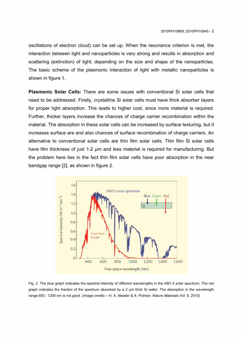
Plasmonic Solar Cells: There are some issues with conventional Si solar cells that
need to be addressed. Firstly, crystalline Si solar cells must have thick absorber layers
for proper light absorption. This leads to higher cost, since more material is required.
Further, thicker layers increase the chances of charge carrier recombination within the
material. The absorption in these solar cells can be increased by surface texturing, but it
increases surface are and also chances of surface recombination of charge carriers. An
alternative to conventional solar cells are thin film solar cells. Thin film Si solar cells
have film thickness of just 1-2 µm and less material is required for manufacturing. But
the problem here lies in the fact thin film solar cells have poor absorption in the near
bandgap range [2], as shown in figure 2.
Fig. 2. The blue graph indicates the spectral intensity of different wavelengths in the AM1.5 solar spectrum. The red
graph indicates the fraction of the spectrum absorbed by a 2 µm thick Si wafer. The absorption in the wavelength
range 650 - 1200 nm is not good. (Image credits – H. A. Atwater & A. Polman, Nature Materials Vol. 9, 2010)
2010PH10869; 2010PH10845 - 3
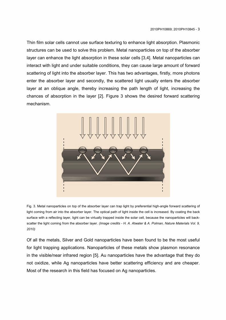
Thin film solar cells cannot use surface texturing to enhance light absorption. Plasmonic
structures can be used to solve this problem. Metal nanoparticles on top of the absorber
layer can enhance the light absorption in these solar cells [3,4]. Metal nanoparticles can
interact with light and under suitable conditions, they can cause large amount of forward
scattering of light into the absorber layer. This has two advantages, firstly, more photons
enter the absorber layer and secondly, the scattered light usually enters the absorber
layer at an oblique angle, thereby increasing the path length of light, increasing the
chances of absorption in the layer [2]. Figure 3 shows the desired forward scattering
mechanism.
Fig. 3. Metal nanoparticles on top of the absorber layer can trap light by preferential high-angle forward scattering of
light coming from air into the absorber layer. The optical path of light inside the cell is increased. By coating the back
surface with a reflecting layer, light can be virtually trapped inside the solar cell, because the nanoparticles will back-
scatter the light coming from the absorber layer. (Image credits - H. A. Atwater & A. Polman, Nature Materials Vol. 9,
2010)
Of all the metals, Silver and Gold nanoparticles have been found to be the most useful
for light trapping applications. Nanoparticles of these metals show plasmon resonance
in the visible/near infrared region [5]. Au nanoparticles have the advantage that they do
not oxidize, while Ag nanoparticles have better scattering efficiency and are cheaper.
Most of the research in this field has focused on Ag nanoparticles.
2010PH10869; 2010PH10845 - 4
EXPERIMENTAL/THEORY:
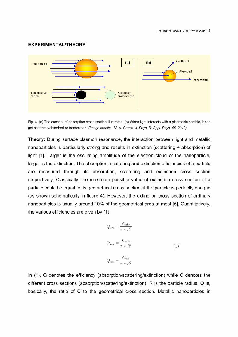
Fig. 4. (a) The concept of absorption cross-section illustrated. (b) When light interacts with a plasmonic particle, it can
get scattered/absorbed or transmitted. (Image credits - M. A. Garcia, J. Phys. D: Appl. Phys. 45, 2012)
Theory: During surface plasmon resonance, the interaction between light and metallic
nanoparticles is particularly strong and results in extinction (scattering + absorption) of
light [1]. Larger is the oscillating amplitude of the electron cloud of the nanoparticle,
larger is the extinction. The absorption, scattering and extinction efficiencies of a particle
are measured through its absorption, scattering and extinction cross section
respectively. Classically, the maximum possible value of extinction cross section of a
particle could be equal to its geometrical cross section, if the particle is perfectly opaque
(as shown schematically in figure 4). However, the extinction cross section of ordinary
nanoparticles is usually around 10% of the geometrical area at most [6]. Quantitatively,
the various efficiencies are given by (1),
(1)
In (1), Q denotes the efficiency (absorption/scattering/extinction) while C denotes the
different cross sections (absorption/scattering/extinction). R is the particle radius. Q is,
basically, the ratio of C to the geometrical cross section. Metallic nanoparticles in
(a) (b)
2010PH10869; 2010PH10845 - 5
plasmon resonance can have Qext greater than 10 i.e., the particle can absorb and
scatter light over a much larger area in its vicinity compared to its geometrical area.
To calculate the absorption and scattering cross section of a nanoparticle whose
diameter is much smaller than the wavelength of light, we can use the dipole
approximation [7], according to (2).
And, Cext = Cabs + Csca, where α is polarizability. For spherical particles, α is given by (3).
In (3), V is the particle’s volume; εp and εm are the dielectric functions, respectively, of
the metal and the medium. We can see that the polarizability increases with volume.
Since Csca ∝ |α|2 while Cabs ∝ Im(∝), larger particles are better at scattering. But we
must keep in mind that the particle must remain sufficiently smaller than the wavelength
of the light for plasmonic interaction. Plasmonic resonance occurs when εp ≈ -2εm is
satisfied. So, the resonance can be tuned by altering the surrounding medium. It can
also be changed by altering the shape of the nanoparticle, as the expression for
polarizability will change [3].
Mie theory provides the exact analytic solution of Maxwell’s equations and is valid for all
spherical particles in homogeneous medium [7]. We performed MATLAB simulations of
Mie Scattering for Ag nanoparticles of different sizes and in different media and
calculated the absorption and scattering efficiencies. We also created 3D models using
COMSOL to study the plasmonic interactions of light with Ag nanoparticles. The goal
was to understand the basics and gain familiarity with simulation software to move on to
the next level – to simulate the plasmonic scattering from an array of interacting
nanoparticles at the interface between two media, which is the case in plasmonic solar
cells; and to optimize the radiative efficiency (Csca/Cext) and minimize the parasitic

2010PH10869; 2010PH10845 - 6
absorption by tuning parameters like nanoparticle size, shape, media and array
configuration. Figure 5 shows the model used for a single Ag nanoparticle.
Fig. 5. The schematic of the model used to simulate the scattering of light by a silver nanoparticle
A scattering of plane wave off the surface of the silver nanoparticle has been performed.
Due to the symmetry of the problem and in order to be able to reduce the computation
time, only one quarter of the sphere has been modelled. Silver sphere has been
surrounded by air, which in turn has been surrounded by a Perfectly Matched Layer
(PML). PML acts as the absorber of the light and prevents its backscattering. It has
been placed at a distance of lambda/2 from the centre of the sphere. The plane which is
perpendicular to the electric field vector is applied Perfectly Electrical Conductor
Boundary Condition (PEC). Similarly the other plane is applied Perfect magnetic
conductor boundary condition, thereby exploiting the symmetry of the problem.
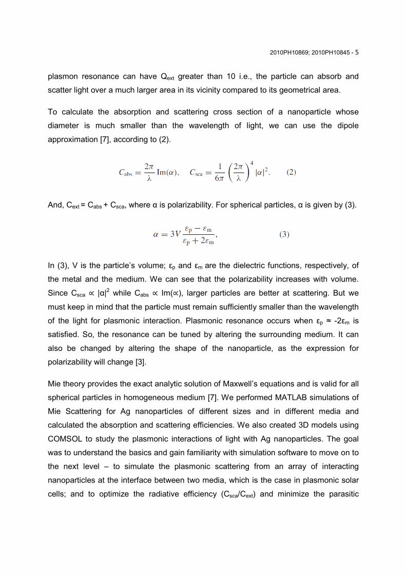
Since real applications of metal nanoparticles would use arrays of nanoparticles and not
a single isolated particle, it is necessary for us to be able to model them. In an array of
nanoparticles net field experienced by a particle is the superposition of the incident field
and the scattered field from the surrounding particles. For simulating the resultant the
scattered field distribution using FEM, we model a single nanoparticle enclosed in a unit
cell and use periodic boundary conditions. According to the periodic boundary condition,
for normal incidence, the magnitude and direction of field at a ‘Master’ boundary is
equal in magnitude and direction to that at the corresponding point of the ‘Slave’
boundary. These boundaries are assigned to the opposite flat surfaces of the unit cell.
One important point which needs attention is that though we are modelling periodic
2010PH10869; 2010PH10845 - 7
array, diffraction effects have not been taken into account because it has been assumed
that the inter-particle separation is much less than the wavelength of light. Moreover,
practically the deposited arrays are seldom periodic. The Transmission factor (T) is then
calculated by dividing the integration value of the poynting vector over the bottom of the
cell (representing transmitted wave) by the value obtained by integration of poynting
vector over the top of the unit cell. The extinction cross section (E) can then be obtained
by E=1-T. Figure 6 shows the model used for simulating a periodic array of interacting
nanoparticles.
Fig. 6. Wire frame of the model used to simulate the periodic array of nanoparticles. (a) Master and Slave boundaries
for periodicity in y-direction. (b) ‘Master’ and ‘Slave’ boundaries for periodicity in x-direction.
RESULTS AND DISCUSSION:
Simulations: The first set of simulations involved MATLAB code to calculate the
scattering, absorption and extinction efficiencies of Ag nanoparticles in continuous
homogeneous media (vacuum and silicon). We performed simulations for particles of
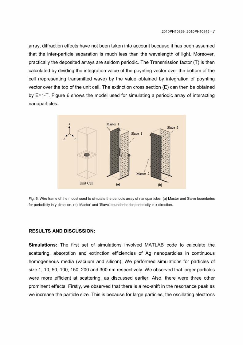
size 1, 10, 50, 100, 150, 200 and 300 nm respectively. We observed that larger particles
were more efficient at scattering, as discussed earlier. Also, there were three other
prominent effects. Firstly, we observed that there is a red-shift in the resonance peak as
we increase the particle size. This is because for large particles, the oscillating electrons
2010PH10869; 2010PH10845 - 8
find it difficult to move together in phase. This causes weaker depolarization field
(driving force behind the oscillations), and hence a lowering of oscillation frequency.
Secondly, we observe that the resonance peak broadens out with an increase in particle
size. This is because larger particles scatter more which causes re-radiation which
causes a damping correction because of which the plasmon resonance peak broadens
[8]. Thirdly, we observe multiple resonance peaks for larger particles, which are
because larger particles cannot be approximated as dipoles, and we must take higher
modes (quadrupole, octapole, etc.) into account.
Fig. 7. Absorption, scattering and extinction efficiencies for Ag nanoparticle of size 50 nm in vacuum.
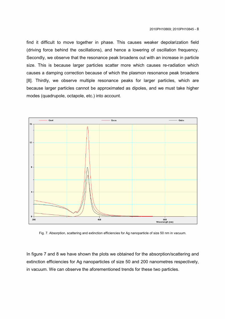
In figure 7 and 8 we have shown the plots we obtained for the absorption/scattering and
extinction efficiencies for Ag nanoparticles of size 50 and 200 nanometres respectively,
in vacuum. We can observe the aforementioned trends for these two particles.
2010PH10869; 2010PH10845 - 9
Fig. 8. Absorption, scattering and extinction efficiencies for Ag nanoparticle of size 200 nm in vacuum.
Fig. 9. Absorption, scattering and extinction efficiencies for Ag nanoparticles of size 50 nm in silicon
One more important observation was that there was a red-shift in the resonance
frequency for a particle in silicon compared to vacuum as shown in figure 9. This can be
understood by considering a sphere in the electrostatic limit. Due to the application of
electric field, charge accumulation takes place at the surface of the sphere resulting in a
dipole. When this sphere is placed in a dielectric, it polarises the dielectric, leading to
the accumulation of bound charge, of opposite sign, at the surface. This accumulated
2010PH10869; 2010PH10845 - 10
charge by reducing the restoring force on the electrons, lowers the resonant energy,
leading to the emission of lower frequencies and hence a red shift.
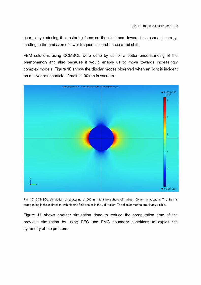
FEM solutions using COMSOL were done by us for a better understanding of the
phenomenon and also because it would enable us to move towards increasingly
complex models. Figure 10 shows the dipolar modes observed when an light is incident
on a silver nanoparticle of radius 100 nm in vacuum.
Fig. 10. COMSOL simulation of scattering of 500 nm light by sphere of radius 100 nm in vacuum. The light is
propagating in the z direction with electric field vector in the y direction. The dipolar modes are clearly visible.
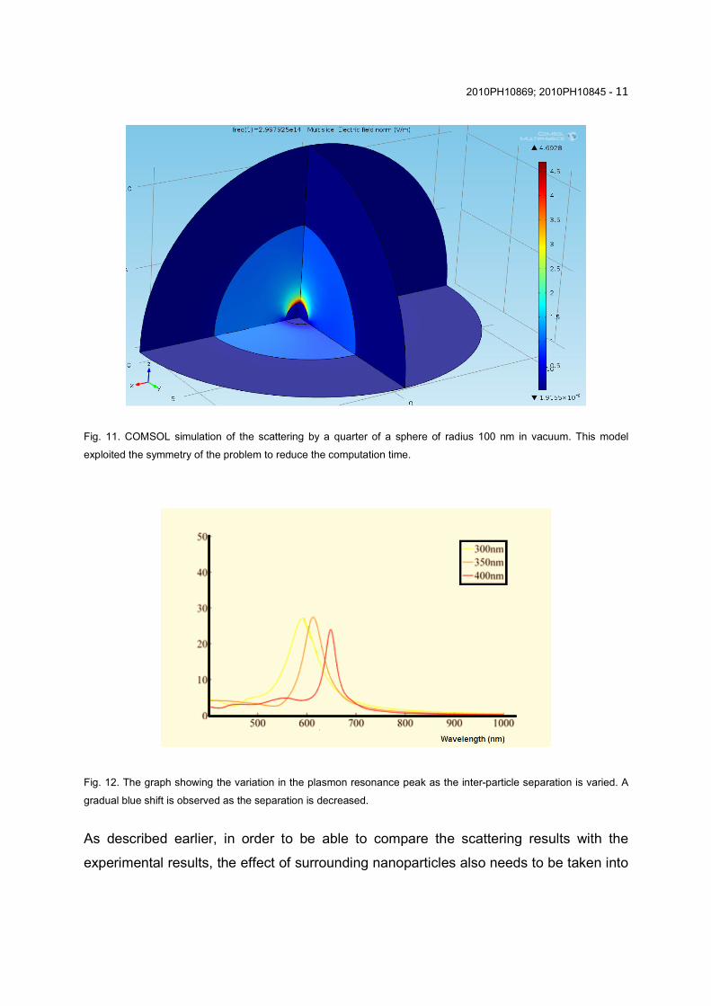
Figure 11 shows another simulation done to reduce the computation time of the
previous simulation by using PEC and PMC boundary conditions to exploit the
symmetry of the problem.
2010PH10869; 2010PH10845 - 11
Fig. 11. COMSOL simulation of the scattering by a quarter of a sphere of radius 100 nm in vacuum. This model
exploited the symmetry of the problem to reduce the computation time.
Fig. 12. The graph showing the variation in the plasmon resonance peak as the inter-particle separation is varied. A
gradual blue shift is observed as the separation is decreased.
As described earlier, in order to be able to compare the scattering results with the
experimental results, the effect of surrounding nanoparticles also needs to be taken into
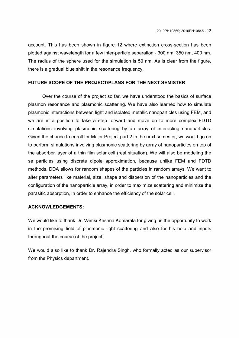
2010PH10869; 2010PH10845 - 12
account. This has been shown in figure 12 where extinction cross-section has been
plotted against wavelength for a few inter-particle separation - 300 nm, 350 nm, 400 nm.
The radius of the sphere used for the simulation is 50 nm. As is clear from the figure,
there is a gradual blue shift in the resonance frequency.
FUTURE SCOPE OF THE PROJECT/PLANS FOR THE NEXT SEMISTER:
Over the course of the project so far, we have understood the basics of surface
plasmon resonance and plasmonic scattering. We have also learned how to simulate
plasmonic interactions between light and isolated metallic nanoparticles using FEM, and
we are in a position to take a step forward and move on to more complex FDTD
simulations involving plasmonic scattering by an array of interacting nanoparticles.
Given the chance to enroll for Major Project part 2 in the next semester, we would go on
to perform simulations involving plasmonic scattering by array of nanoparticles on top of
the absorber layer of a thin film solar cell (real situation). We will also be modeling the
se particles using discrete dipole approximation, because unlike FEM and FDTD
methods, DDA allows for random shapes of the particles in random arrays. We want to
alter parameters like material, size, shape and dispersion of the nanoparticles and the
configuration of the nanoparticle array, in order to maximize scattering and minimize the
parasitic absorption, in order to enhance the efficiency of the solar cell.
ACKNOWLEDGEMENTS:
We would like to thank Dr. Vamsi Krishna Komarala for giving us the opportunity to work
in the promising field of plasmonic light scattering and also for his help and inputs
throughout the course of the project.
We would also like to thank Dr. Rajendra Singh, who formally acted as our supervisor
from the Physics department.
2010PH10869; 2010PH10845 - 13
REFERENECES:
[1] M. A. Garcia, “Corrigendum: Surface plasmons in metallic nanoparticles: fundamentals and applications”, J.
Phys. D: Appl. Phys. (2012).
[2] Harry A. Atwater and Albert Polman, “Plasmonics for improved photovoltaic devices”. Nature Materials, vol. 9,
2010.
[3] R. Santbergen, T. L. Temple, R. Liang, A. H. M. Smets, R. van Swaaij and M. Zeman, “Application of plasmonic
silver island films in thin-film silicon solar cells”. J. Opt., Vol. 14, 024010 (10pp), 2012.
[4] K. R. Catchpole and A. Polman, “Plasmonic Soar Cells”. Optics Express, Vol. 26,No. 26, 21793 (7pp.) 2008.
[5] Eshwar Thouti, Nikhil Chander, Viresh Dutta and Vamsi K Komarala, “Optical properties of Ag nanoparticle
layers deposited on silicon substrates”. J. Opt., Vol. 15, 035005 (7pp), 2013.
[6] Leatherdale CA, Woo WK, Mikulec FV, Bawendi MG, “On the Absorption Cross Section of CdSe Nanocrystal
Quantum Dots”. Journal of Physical Chemistry B., Vol. 106, 7619-7622, 2002.
[7] Bohren C F and Huffman D R 2004 Absorption and Scattering of Light by Small Particles (Weinheim: Wiley).
[8] A. Wokaun, J. P. Gordon, and P. F. Liao, "Radiation damping in surface-enhanced Raman scattering," Phys.
Rev. Lett. Vol. 48, 957, 1982.