metal oxide composite enabled nanotextured si photoanode for efficient solar driven water oxidation
TRANSCRIPT

Metal Oxide Composite Enabled Nanotextured Si Photoanode forEfficient Solar Driven Water OxidationKe Sun,† Xiaolu Pang,‡ Shaohua Shen,§ Xueqiang Qian,‡ Justin S. Cheung,† and Deli Wang*,†,∥,⊥
†Department of Electrical and Computer Engineering, University of California, San Diego, La Jolla, California 92093, United States‡Department of Materials Physics and Chemistry, University of Science and Technology Beijing, Beijing 100083, China§State Key Laboratory of Multiphase Flow in Power Engineering, Xi’an Jiaotong University, Xi’an, Shaanxi 710049, China∥Material Science Program and ⊥California Institute of Telecommunication and Information Technology, University of California,San Diego, 9500 Gilman Drive, La Jolla, California 92093, United States
*S Supporting Information
ABSTRACT: We present a study of a transition metal oxidecomposite modified n-Si photoanode for efficient and stablewater oxidation. This sputter-coated composite functions as aprotective coating to prevent Si from photodecomposition, aSchottky heterojunction, a hole conducting layer for efficientcharge separation and transportation, and an electrocatalyst toreduce the reaction overpotential. The formation of mixed-valence oxides composed of Ni and Ru effectively modifies theoptical, electrical, and catalytic properties of the coatingmaterial, as well as the interfaces with Si. The successful application of this oxide composite on nanotextured Si demonstratesimproved conversion efficiency due to enhanced catalytic activity, minimized reflection, and increased surface reaction sites.Although the coated nanotextured Si shows a noticeable degradation from 500 cycles of operation, the oxide composite providesa simple method to enable unstable photoanode materials for solar fuel conversion.
KEYWORDS: Solar water oxidation, electrocatalyst, nanotextured Si
An optical band gap of 1.12 eV makes Si, the second mostearth abundant material, a very attractive candidate for
solar fuel conversion. However, the fundamental photo-electrochemistry properties of Si, when in contact with aqueoussolution, do not favor Si for solar water splitting, in which solarenergy is typically converted and stored in chemical bonds.Thermodynamic oxidation potential of Si is above the wateroxidation level, which introduces a competition reaction whenoperating with energetic holes.1 This oxidation effectivelypassivates the Si, which also becomes a concern when p-Siphotocathode is in idle condition2 or has to go through adestructive subsequent coating process.3 Moreover, having asignificantly higher conduction band edge of Si to the protonreduction level results in a slow charge transfer kinetics. Thisfact limits the conversion efficiency of Si-based photoelectrodewhen directly interfacing with electrolyte. To replace thistroublesome interface at the Si/electrolyte junction, a newconformal and rectifying junction is essential to suppress theself-oxidation and improve the kinetics.4 Structures usinghomogeneous junctions through surface inversion have beenutilized to solve aforementioned problems and have beendemonstrated on both n and p-type Si photoelectrode.5 On theother hand, strategies using heterogeneous coatings on Siphotoelectrode have also been developed using moleculesurface functionalization, metals, alloys, or other semiconduc-tors.6
Theoretically, a rectifying junction relies on the workfunction difference between the coating material and Si. Forn-Si, a coating with a high work function is essential to form arectifying junction to separate the free charges. However, highwork function metals such as Pt or Pd have inferior oxygenevolution reaction (OER) catalytic activity compared to Ir orRu. Meanwhile, they are typically of high cost and limitedresources, which are the main obstacles for large scaleapplications of noble metals in catalysis. In addition, noblemetals are not stable in alkaline environment.7 On the otherhand, earth abundant transition metal oxides (such as Mn, Fe,Co, and Ni) show typically lower activity8 but reasonablestability in alkaline environment. Furthermore, metal oxideoutperforms metal because metal oxide can achieve a muchhigher work function than metals due to oxygen vacancies andcation oxidation states.9 The work function of a transition metaloxide can be tuned through the incorporation of other metal ormetal oxides. In addition, metal oxide can minimize the opticalloss due to a typically larger optical band gap. Moreover, metaloxides with technically unlimited combinations are typicallystable and nontoxic. Therefore, this stable metal oxide coatingwith a high work function and high transmittance is desired for
Received: January 27, 2013Revised: March 15, 2013Published: April 10, 2013
Letter
pubs.acs.org/NanoLett
© 2013 American Chemical Society 2064 dx.doi.org/10.1021/nl400343a | Nano Lett. 2013, 13, 2064−2072
unstable n-type photoanode materials to form a Schottkybarrier to assist the transportation of photoexcited holes to thereductant in the electrolyte and to maximize the amount ofphotons arriving at the underneath photoactive material.From a design point of view for an optimized junction, a p-
type coating with a higher hole-conductivity is essential. Nioxide is intrinsically p-type and Ni-based oxides showed greatpotential. Doped or mixed nickel oxide is recognized as one ofthe promising OER catalyst that showed great stability in analkaline environment.10 Other applications of mixed-valence Nioxide, such as supercapacitors,11 batteries, fuel cells, and dye-sensitized solar cells,12 were demonstrated because of itstunable functionalities. Ru oxide has been known as anexcellent candidate for electrochemical capacitors due to itsfast and reversible reduction/oxidation reactions from protonadsorption/desorption.13 Meanwhile, Ru and its oxide are alsoknown as the best OER catalysts. Applications of RuOx toimprove the water oxidation reaction have been demonstratedbefore in some milestones solar driven water splitting devices.14
Actually, the oxide composite (NiRuOx) has also demonstratedapplications as electrical contact,15 pseudocapacitor electrode,16
and OER catalyst.7
We hypothesize that (i) an oxide mixture of NiOx with asmall amount of RuOx can maintain the stability of NiOx coatedSi-based photoanode, and (ii) by controlling the synthesiscondition this composite can improve the catalytic activity andthus improve the conversion efficiency of Si-based photoanode.In this work, we report a single-step protection and catalysisusing a composite of Ru and Ni oxides on an n-type Siphotoanode. This composite protects the Si photoanode fromdirect contact with the oxidizing water and thus prevents thephotoanodic passivation of Si. The nanometer scale coatingmaintained its integrity and functionality during the long-termoperation. Therefore, this composite coating eliminates theneed for extra process of protection. The composite with a lowresistivity significantly minimized the kinetic energy loss duringthe charge traveling across the coating to oxidize water. Therectifying junction between mixed oxides and Si improvedcharge transport and collection efficiency. The compositecoated Si photoanode showed comparable activity to that of theRu metal directly coated Si. Finally, we also demonstrated thata conformal coating of this composite on a nanotextured blackSi photoanode can further improve the water oxidationefficiency.Various strategies were developed to suppress the self-
passivation of n-Si as well as other unstable photoanodematerials under anodic bias and under illumination. Consid-erable success has been made using heterogeneous coatingfrom various method, such as TiO2,
17 ITO,18 Fe2O3,19
MnO2,6h,20 CoPi,21 and NiO.22 Nonstoichiometric NiO
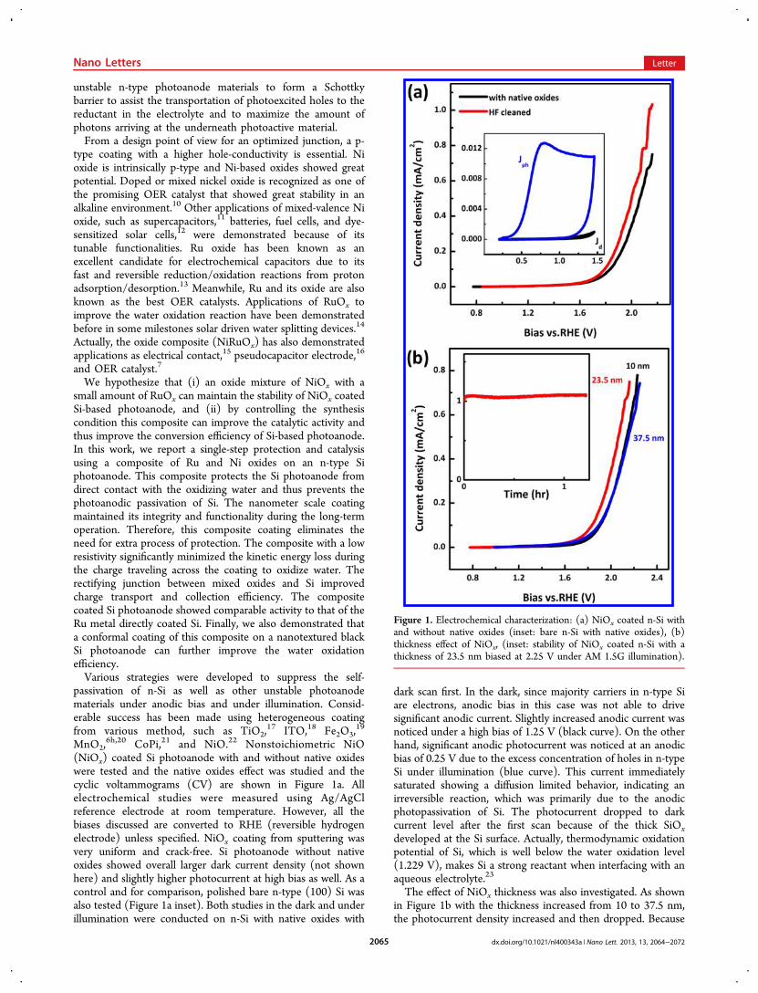
(NiOx) coated Si photoanode with and without native oxideswere tested and the native oxides effect was studied and thecyclic voltammograms (CV) are shown in Figure 1a. Allelectrochemical studies were measured using Ag/AgClreference electrode at room temperature. However, all thebiases discussed are converted to RHE (reversible hydrogenelectrode) unless specified. NiOx coating from sputtering wasvery uniform and crack-free. Si photoanode without nativeoxides showed overall larger dark current density (not shownhere) and slightly higher photocurrent at high bias as well. As acontrol and for comparison, polished bare n-type (100) Si wasalso tested (Figure 1a inset). Both studies in the dark and underillumination were conducted on n-Si with native oxides with
dark scan first. In the dark, since majority carriers in n-type Siare electrons, anodic bias in this case was not able to drivesignificant anodic current. Slightly increased anodic current wasnoticed under a high bias of 1.25 V (black curve). On the otherhand, significant anodic photocurrent was noticed at an anodicbias of 0.25 V due to the excess concentration of holes in n-typeSi under illumination (blue curve). This current immediatelysaturated showing a diffusion limited behavior, indicating anirreversible reaction, which was primarily due to the anodicphotopassivation of Si. The photocurrent dropped to darkcurrent level after the first scan because of the thick SiOxdeveloped at the Si surface. Actually, thermodynamic oxidationpotential of Si, which is well below the water oxidation level(1.229 V), makes Si a strong reactant when interfacing with anaqueous electrolyte.23
The effect of NiOx thickness was also investigated. As shownin Figure 1b with the thickness increased from 10 to 37.5 nm,the photocurrent density increased and then dropped. Because
Figure 1. Electrochemical characterization: (a) NiOx coated n-Si withand without native oxides (inset: bare n-Si with native oxides), (b)thickness effect of NiOx, (inset: stability of NiOx coated n-Si with athickness of 23.5 nm biased at 2.25 V under AM 1.5G illumination).
Nano Letters Letter
dx.doi.org/10.1021/nl400343a | Nano Lett. 2013, 13, 2064−20722065

of the trade-off between increased depletion of Si and seriesresistance loss on thick NiOx film, an optimum thicknessconfiguration should be expected when one of the parameters isdominant over the other. In our case, we have found that NiOxfilm with a thickness of 23.5 nm was able to provide smaller on-set potential and better photocurrent density. The ampermetricstudy at a constant bias voltage of 2.25 V revealed a stablephotoanode without noticeable signs of photocurrent degrada-tion in the first 90 min of operation (Figure 1b inset).Compared to previous reported work, the sputtered filmshowed inferior activity but extended lifetime.22 This is believeddue to the compact protective film that did not develop pin-holes and thus pathways for oxidation of Si underneath duringthe operation. Apparently, improvement to further lower theexternal bias is needed to drive a considerable current densityfor consecutive chemical conversion.The oxide composite (NiRuOx) was synthesized using
cosputtering technique and detailed deposition conditions canbe found in the Supporting Information. Optical transmittanceof the NiOx and NiRuOx on cleaned soda lime glass substrateswas measured and shown in Figure 2. Morphology of thecoating before and after annealing did not show significant
changes (Figure 2a insets). On the NiOx sample, transmittanceabove 400 nm improved from 91 to 98% after annealing. Thisincrease of transmittance at long wavelength maybe due to theenhancement of crystallinity with the thermal treatment, as wellas out-diffusion of interstitial O atoms that acted as scatteringcenters to the incident light.24 On the other hand, the as-prepared NiRuOx sample before annealing showed a lessrecognizable band edge transition. Moreover, the transmittanceof NiRuOx at wavelength above 400 nm was reduced afterannealing. The transition in the wavelength range of 300−400nm appeared to be steeper after annealing due to the stronginterband absorption of NiOx. The direct band gap, owning tothe unoccupied Ni 3d and mixed O 2p/Ni 3d, fromextrapolating the linear portion of the Tauc relation (αhυ2 vshυ) showed a blue shift for annealed samples from 3.33 to 3.66eV for NiOx and 2.96 to 3.37 eV for NiRuOx (Figure 2b). Thisobservation suggests a reduced density of structural defects andsurface states under thermal treatment conditions that couldcontribute to the intraband absorption.25 However, tails in theannealed NiRuOx film (Figure 2b black curves) suggest anexisting multiple-interband transition besides the defects andsurface states, presumably due to the smaller band gap ofRuOx.
26 Van der Pauw resistivity measurement on NiOx andNiRuOx samples revealed the reduced resistivity through theincorporation of Ru and thermal treatment processes. Ohmiccontact with low resistivity was achieved using a sandwichlayered ITO/Au/ITO structure deposited using gas phasesputtering. Detailed data on the ohmic contact and rectifyingjunction (Supporting Information Figure s1) and the resistivityof the composite before and after annealing (SupportingInformation Table s1) can be found in Supporting Information.X-ray photoelectron spectroscopy (XPS) studies and
deconvoluted peaks of the spectra of the annealed NiOx andNiRuOx film are shown in Figure 3. Interpretation of Ni 2pXPS spectrum can be difficult because of multiple splitting,shakeup, and plasmon loss.27 It has been pointed out byGrosvenor et al. that it was difficult to assign single state to onepeak.28 However, since Ni(III) states dominated at higherenergy level in the main peak,27 we adopted a simple two peakfitting on the main Ni 2p3/2 peak to study the Ru effect on theNiO.28 Ni 2p spectrum shown in Figure 3a suggests that thesputtered NiOx exhibited coexisting valence states of Ni(II)2p3/2 (binding energy at 854.04 eV) and Ni(III) 2p3/2(binding energy at 855.53 eV) (top curve in Figure 3a). On theother hand, composite NiRuOx (bottom curve in Figure 3a)showed significantly lower Ni(II)/Ni(III) ratio in the main Ni2p3/2 peak compared to that of the pristine NiOx film,indicating an increase of valence state of Ni and an oxygen-richcomposite film. Meanwhile, interstitial O atoms in the oxygen-rich NiRuOx composite could cause scattering or absorb theincident light, which also support the observation of reducedtransmittance in the visible range and thus absorption tales intolonger wavelength (Figure 2).The Ru 3d5/2 peak with a binding energy at 281.12 eV and a
spin−orbit splitting 3d3/2 of 285.11 eV revealed that Ru in theannealed NiRuOx composite was mainly composed of Ru(IV)in the oxidized state (Figure 3b). XPS spectra by peak fittingrevealed the extra component at 282.16 eV with its splittingpeak at 286.32 eV. Note that the XPS spectrum in the rangeshowing in Figure 3b also includes superimposed C1s core-level(284.8 eV) besides Ru 3d level causing an intense Ru 3d3/2peak. Deconvolution of the XPS spectrum is consistent withprevious reported data.29 This component was believed due to
Figure 2. (a) Optical transmittance of oxide composite films beforeand after annealing. Inset: NiOx (first row) and NiRuOx (second row).Scale bar = 200 nm. (b) Tauc plots for NiOx and NiRuOx before andafter annealing.
Nano Letters Letter
dx.doi.org/10.1021/nl400343a | Nano Lett. 2013, 13, 2064−20722066

the unscreened Ru(IV) cations30 or it could be also anindication of higher oxidation states of Ru coexisting such asRu(VI) or Ru(VIII).29 Note that the metal peak of Ru (∼280.4eV) was not noticed on annealed samples without experiencingAr ion beam etching even with higher Ru concentration,confirming a complete Ru oxidation in the composite afterannealing.Further investigation on the O 1s XPS spectrum (Figure 3c)
revealed three peaks corresponding to classical oxygen atoms inthree different environment in the sputtered NiOx filmincluding lattice oxygen (529.85 eV), hydroxyl group (531.66eV), and surface-absorbed water (532.6 eV). These data arealso in agreement with previous reported ones.31 Additionalfeatures (gray curves) in the O 1s spectrum of NiRuOx incomparison to the one from the pristine NiOx were due to theoxygen binding in the RuOx corresponding to the latticeoxygen at 529.4 eV and hydroxyl group at 530.59 eV, as well asand surface-absorbed water overlapping with the one on NiOxat 532.6 eV. Similar to the NiOx, NiRuOx sample also showedstronger hydroxyl component and weak surface absorbed watercomponent. This observation suggested that oxyhydroxide mayform resulting in a higher Ru oxidation state at the surface dueto the exposure of ambient atmosphere. Importantly, areas ofthe deconvoluted curves can be used to semiquantitativelyestimate the ratio of the Ni(II)/Ni(III), which decreasessignificantly from about 0.86 in NiOx to 0.35 in NiRuOx. This
indicated a Ni(III)-rich film was introduced by incorporation ofRuOx consistent with the observation on Ni 2p peaks.For electrochemical characterization, we directly deposited
the NiOx and NiRuOx composite film on fluorine doped tinoxide (FTO) coated glasses (12−14 Ω/□, thickness <200 nm,TEC 15 Hartford Glass Co.). To avoid interactions betweencoating and the FTO film and to avoid high-temperaturedegradation of the FTO conductivity, the sintering temperaturewas kept at 400 °C in inert N2 environment. The voltammo-grams without additional iR correction are shown in Figure 4.
FTO glass electrode showed the highest onset potential to passthe double-layer current region. Application of NiOx with athickness of 23.5 nm exhibited a catalyzed reaction by reducingthe potential needed to drive the same level of current (Figure4a). In the medium bias region of 1−10 mA/cm2 whenFaradaic process occurred, Tafel slopes were measured of 484mV/dec for FTO glass and 290 mV/dec for FTO|NiOx (Figure4a inset). Overpotentials at 10 mA/cm2 for FTO glass andFTO|NiOx were 1829 mV and 1043 mV, respectively. Coatingof NiOx on FTO reduced the overpotential needed to drive theanodic water decomposition current. Compared to NiOx OER
Figure 3. XPS spectrum of NiOx and NiRuOx composite: (a) Ni 2p,(b) Ru 3d and C1s, and (c) O 1s.
Figure 4. Electrochemical characterization of NiOx and NiRuOxcomposite coated FTO glass: (a) linear voltammograms; inset, Tafelplots. (b) Cyclic voltammograms of 5 consecutive scans; inset,magnified red curve.
Nano Letters Letter
dx.doi.org/10.1021/nl400343a | Nano Lett. 2013, 13, 2064−20722067

electrocatalyst reported before, the sputtered film showedinferior catalytic activity. A dense and pinhole free film isneeded to protect Si from contacting the oxidizing electrolyteand minimize the chances of penetration of electrolyte throughgrain boundaries. Often cases, a thicker film from sputtering canmeet this specification and prevent the anodic passivation of Si.This dense and thick NiOx film with limited surface reactionsites and high electronic ohmic loss (Supporting InformationFigure s1 and Table s1) resulted in the poor catalyticperformance. Addition of Ru lowered the onset potential, aswell as the Tafel slope to 212 mV/dec Meanwhile, anoverpotential needed to achieve 10 mA/cm2 current was alsoreduced to 797 mV from the composite coating. The increasein Tafel slope at high current densities (>10 mA/cm2)occurring at the electrode surface was due to the resistivecontrolled kinetics, such as series resistance loss fromelectrolyte and formed bubbles on the surface. None of thefresh prepared samples showed light response with a noticeablephotocurrent. Cyclic voltammograms (CV) within a potentialwindow of 0.2−1.4 V were obtained at a 100 mV/s scan rate.Redox response at 0.6−1.3 V due to the pseudocapacitvebehavior of NiOx was observed (Figure 3b inset). The cathodiccurrent was believed due to the reduction of NiOO2 to NiOOHand NiOOH to NiO of different phases. A more significantrectangular shape characteristic of the pseudocapacitance due toRuOx was exhibited (Figure 3b). A much more pronouncedamount of charges was stored and associated with the Ru redoxprocess (blue curve) in the potential window compared toFTO|NiOx (red curve) and bare FTO electrodes (black curve).The peaks corresponding to oxidation and reduction of thedifferent Ru oxidation states in RuO2 were noticed. Thepresence of these features was a strong indication that redoxprocess also occurred on the RuO2, which arises when theapplied potential induces Faradaic current from the oxidation/reduction of electroactive materials via a coupled and reversibleproton−electron transfer,13 suggesting a catalytic active Ru inthe composite film.To demonstrate further the advantages of NiRuOx as a
catalytic and protective coating on n-Si, we have compared thisc-Si|NiRuOx structure to a Si photoanode directly coated withRu (c-Si|Ru) and one with a high quality ultrathin TiO2protection layer in-between (c-Si|TiO2|Ru). For example,Chen et al. used TiO2 from atomic layer deposition (ALD)to protect n-Si photoanode from anodic photopassivation.32
Pracchino et al. showed the extended lifetime of a unstablephotocathode (p-Cu2O) by effective passivation using TiO2.
33
Recently, Lee et al. demonstrated this protective coating onIII−V (p-InP) photocathode.34 While providing excellentchemical stability, the ultrathin TiO2 with a thickness of 2nm maintained the effective charge transfer of excited carriers.In these works, electrocatalysts were then deposited on top ofTiO2 to lower the reaction overpotential and enhance currentdensity. This so-called “two-step process” utilizes a protectionlayer (TiO2) and an electrocatalyst layer (noble metal)separately. The thickness of TiO2 is important particularly onn-type photoanode materials to maintain its light response(Supporting Information Figure s2), since TiO2 prepared fromvarious method is a well-known photoactive specifically toultraviolet (UV) light. Without an outperforming catalyst,ultrathin TiO2-coated crystalline n-Si (c-Si|TiO2) photoanodestill requires a large overpotential to drive the water oxidationreaction (Supporting Information Figure s3). Ru metaldeposited on c-Si|TiO2 photoanode effectively lowered the
onset potential due to its superior OER catalytic activity. Thephotocurrent density from c-Si|TiO2|Ru at 1.23 V was able toreach 0.24 mA/cm2 (Supporting Information Figure s3).However, this value is around 4 times lower compared to thephotocurrent density of 1.06 mA/cm2 from the c-Si|Ruphotoanode. This is believed due to the additional loss oftunneling carriers across the TiO2 coating and low kinetics.6f,g
The high dark current from c-Si|Ru was due to the metal-induced intermediate surface states, which resulted in a muchlower on/off ratio of current (jph/jd at overpotential of 230mV). On the other hand, the c-Si|NiRuOx photoanode showeda similar photocurrent density to that of the c-Si|Ru sample at1.23 V but much higher on/off ratio due to the suppressed darkcurrent. Meanwhile, c-Si|Ru showed quicker degradation underoperation conditions. As shown in Supporting InformationFigure s4, photocurrent density dropped below half of theinitial value in less than 20 min, despite its slightly higher initialphotocurrent density than that of the c-Si|NiRuOx. Note that tobe comparable, Ru loading on all the samples were constant bycontrolling the deposition conditions (Supporting Informa-tion). Comparisons between aforementioned structures aresummarized in Table 1.
Surface textures effectively enhance the light utilization,increase the surface reaction sites, and minimize the bubbleoverpotential through a hydrophilic surface.34,35 P-type Si withsurface textures used as photocathodes for water reduction andH2 generation was demonstrated before.2,5c,36 Nanotextured Si(or black Si, b-Si) were generated through a facile chemicaletching at room temperature, which is well documented37 anddetails can be found in Supporting Information. Themorphology as a function of the etching time is shown inSupporting Information Figure s5a-e. The depth of thenanotextured layer increased with the etching time. Thisetching process has a linear relationship with the etching time,before there is a significant chemical depletion and limitedreactant diffusion due to the developed thick metal coating.Estimated etching rate at room temperature was about 1.55nm/s (black ▲ curve in Supporting Information Figure s5f).Rough estimation on surface area showed a linear relationshipwith the etching time assuming no loss in the density of poreson the surface over time. However, this assumption may not be100% true as seen in the SEM images in the second row inFigure s5a-e, due to the lateral overetching and increased fillingfactor of pores which led to a decrease in the surface area.Roughness factor estimated from SEM images are 2, 3.8, 8.6,11.5, and 12.6 for samples with 1, 2, 5, 8, and 15 min etching,which is actually saturated with the increasing etching time(blue ■ curve in Supporting Information Figure s5f). This isone of the reasons that we did not use longer etching time toachieve deeper pores. The geometry of the b-Si is actually
Table 1. Comparisons between Different PhotoanodeStructures for Water Oxidation
jph/jd @ η =230 mV
onsetpotential(V)
jph (mA/cm2)@ 1.23 V
time for 50%drop of jph
c-Si|NiRuOx
67.57 1.08 0.94 >1 h
c-Si|Ru 12.91 1.08 1.06 <20 minc-Si|TiO2|Ru
6.57 1.17 0.24 NA
c-Si|TiO2 NA 2.46 4.31 ×10⁴ NA
Nano Letters Letter
dx.doi.org/10.1021/nl400343a | Nano Lett. 2013, 13, 2064−20722068

critical. Additional reasons for using an 8 min etched b-Si willbe given in the later discussions.Si photocathode for proton reduction is considerably stable
under illumination and cathodic bias in an acidic environ-ment.36a However, its stability does become a concern when inidle condition, under anodic bias, or alkaline electrolyte, whereproper protection is needed.3 Therefore, a high quality andconformal protection layer is particularly important to enable Sifor water oxidation since the n-Si is typically anodically biasedand excess carriers of holes. Gas phase deposition offersopportunities to reach a uniform coating on high-profilestructures and offers minimum chances for exposure ofsubstrates. Magnetron RF sputtering in this experiment wasable to provide conformal coating on the b-Si with etchingdepth of 680 nm. However, with the increased depth in b-Si, aconformal coating became difficult and eventually failed wheresignificant degradation of photoresponse was observed. This isanother reason of using 8 min textured b-Si as the substrate forthe demonstration of NiRuOx composite enabled Si photo-anode.The morphology of the b-Si substrate with a 680 nm thick
porous layer on the surface is shown in Figure 5a,b. Specularreflection spectra of mirror-polished c-Si and nanotextured b-Siare shown in Figure 5c. The experimental verification of thespecular reflectance discussed above was measured at a fixedincident angle of 30°. c-Si showed significant UV reflection withreflectance above 55% at wavelength below 400 nm. Atwavelength between 400 and 700 nm, polished Si showedaverage reflectance of 41.8% and an average specular reflectanceof 37.0% in the near-infrared (IR) and IR range (wavelengthbetween 700 and 1100 nm), which is consistent with previousreported data.38 For comparison, this b-Si showed a wide rangesuppression of reflection. The ultralow specular reflectivity wasreached in the entire wavelength range of 350 to 1100 nm dueto the effective coupling of incident light to the Si substrate.One of the primary physical effects behind this phenomenon is
the change of the refractive index at the air and Si interface. Thetransition of the refractive index was effectively modulated andsmoothed by the porous Si layer, resulting in the reducedspecular reflectance, enhanced internal reflection, and thusenhanced absorption. A reflectance dip at wavelength around640 nm indicated a strong resonance corresponding to physicalgeometry of the porous layer.39 Although reflectance increasedat wavelength above 700 nm, nanotexturing technique showeda broadband suppression of reflection due to the effectivecoupling of light offered by the porous layer. The optical imageclearly showed the reflective nature of the polished Si where thereflection of the imaging camera can be seen (right image inFigure 5c inset) and the black appearance of the etched Si (leftimage in Figure 5c inset).Linear voltammograms of NiRuOx composite coated c-Si and
b-Si are shown in Figure 5d. Both photoanodes showednegligible dark currents. At 1.23 V, NiRuOx composite coatedb-Si showed photocurrent density of 1.34 mA/cm2, about 1.5times greater than that of the c-Si|NiRuOx photoanode. Theenhanced photocurrent density is due to the increased surfacearea under a fixed geometrical area (11.5 times larger) andimproved light absorption. Catalytic reaction mechanism andoxygen evolution at both Ni and Ru sites can be generallydescribed using equations below and illustrated in the Figure 5dinset
→ +− +e hSihv
(1)
+ + → ++ + − +hM H O M (OH ) Hn n2
1ad (2)
→ + ++ − +2M (OH ) M O M H On n n1ad
22 (3)
→ ++2M O 2M On n22 (4)
where Mn is the metal active site (Ni and Ru with valence statesof n+).
Figure 5. NiRuOx coated black Si: SEM image (a) top view and (b) cross-sectional view. Scale bar = 200 nm. (c) Specular reflectance on c-Si and b-Si. Insets: digital optical images of c-Si (right) and b-Si (left). (d) Comparison of linear voltammograms. (e) Cyclic voltammograms of b-Si|NiRuOxat varying light intensity. (f) Vocph, Vonset, [email protected] V, and j@432 mV overpotential versus light intensity. (g) IPCE spectrum and (h)chronoamperometric stability study in 500 cycles operation.
Nano Letters Letter
dx.doi.org/10.1021/nl400343a | Nano Lett. 2013, 13, 2064−20722069

Current fluctuation in the polarization study was reduced onthe b-Si samples, which was believed due to the hydrophilicproperty of b-Si surface and reduced radius of curvature ofnanowires. These facts eased the bubble release from electrodesurfaces upon formation without contributing overpotentiallosses from large bubbles forming.35 Importantly, significantimprovement in light absorption and surface area did notimprove the photocurrent dramatically. This is primarilybecause of the increased surface defects and thus recombinationvelocity.40 In fact, nonoptimized electrodes displayed higheronset potential. These electrodes, for example, include sampleswith films deposited at higher O2 partial pressure during thesputtering process, or annealed in O2 environment duringanneal process. Increased O2 partial pressure improves theoxygen vacancy and also reduces the electrical resistivity, thiscould also cause of a loss of transmittance due to interstitial Oas scattering centers.24 As mentioned in the early discussion,electrodes coated with thicker NiOx film also showed inferiorperformance. In addition, poor ohmic contact or high contactresistance could also increase the onset potential. All of thesenonoptimized fabrication conditions contributed to theincreased O2 evolution reaction overpotential resulting in ahigher external driving bias and lower conversion efficiency.The CV curves of b-Si|NiRuOx sample under different light
intensities are shown in Figure 5e. With the reduced lightintensity by applying a series of neutral density (ND) filters, wenotice a continuous decrease of photocurrent density in thesame bias range. At low light intensity, it was noticed that theintensity of the shoulder at 1 mA/cm2 reduces and also it shiftsto high bias value. This indicates a slow process presumably dueto the limited OH− ion diffusion in the near neutral solution.7
Current saturation was not noticed in the range of themeasured bias at intensity of 100 mW/cm2 and started toappear at incident light intensity below 10 mW/cm2 due to thelimited density of excess carriers. The saturation point shifts tolower bias values with the reduced light intensity. Voc underillumination (Vocph) shifted to more positive values with thereducing light intensity and eventually approached the Voc valueat dark (Vocd) due to the reduced quasi-Fermi level separation.Note that the Voc here is defined as the current shifts fromcathodic to anodic direction. To confirm the stability of thesample, cyclic voltammograms were remeasured under normalincident at a light intensity of 100 mW/cm2. Slight decrease(<5%) in current density over the scanned bias range wasnoticed indicating a minimal degradation.The bias to maintain a certain current density (0.2 mA/cm2)
as a function of light intensity is primarily controlled by theinterfacial property of b-Si|NiRuOx and catalytic activity of thecomposite, as shown in Figure 5f (black square curve). Thisonset potential for water oxidation shifts to lower valuesexponentially with the increased incident light intensities, whichwas expected as the Vocph decreased (red ● curve). Therefore,the voltage difference (|1.23-Voc|) increases exponentially withincreasing incident light intensity, since the Voc in a solar cellgenerally depends on the logarithm of the photogeneratedcurrent density. The Voc versus light intensity in logarithm scaleis shown in Supporting Information Figure s6. The sign of theslope indicating the photoanodic behavior of the Si|NiRuOxphotoelectrode.41 Meanwhile, photocurrent densities showedsimilar behavior as the Voc (Figure 5f). For example, at thethermodynamic water oxidation potential (1.23 V), thephotocurrent density increased exponentially with the increas-ing light intensity and finally approaching a saturated value of
1.36 mA/cm2 at 100 mW/cm2 (blue ▲ curve). Photocurrentdensity at 432 mV overpotential (brown ▶ curve) alsoexponentially increased with the increasing light intensity whichfollowed the same trend as the photocurrent density atthermodynamic potential. The photocurrent density at thisoverpotential can be as high as 7.44 mA/cm2 at an incidentlight intensity of 200 mW/cm2.The incident-photon-conversion efficiency (IPCE) as a
function of wavelength for the b-Si|NiRuOx photoanode at432 mV overpotential is shown in Figure 5g. The exposed areaon the sample was fixed at 1 cm2 controlled by the window sizeon the sample holder. The spot size (Aph = 0.1 mm × 0.2 mm)of the monochromated light on the sample surface was muchsmaller than the sample size. This was considered in the IPCEcalculation where the photocurrent was calculated using theequation below
=−
jI I
Aphph d
ph (5)
where Iph and Id is the current measured under chromated lightillumination and in dark, respectively, and Aph is the light spotsize. The light intensity of the monochromated light from themonochromator equipped with an IR filter on the samplesurface was calibrated using a Si photodetector at zero bias.IPCE was calculated using the equation below
λ
η
=· · × ·
×
= ×·
·
− −
·
·−
−
λ
−
−
j
j
j
IPCE1240[nm mW mA ] [mA cm ]
[nm]
[mA cm ]
[mA cm ]
j
R
1ph
2
[mA cm ]
[mA mW ]
extph
2
phD2
phD2
1
(6)
where λ is the wavelength of incident light in nm, jphD is thephotocurrent from the Si photodetector in mA/cm2, Rλ is theresponsitivity of the Si photodetector provided by the supplierin mA/mW, and ηext is the external quantum efficiency of the Siphotodetector. The shape of the IPCE curve matched well withthe typical Si solar cell showing response between 350 and1100 nm with effective photocurrent generated in thewavelength range of 475−725 nm. With the increased surfacearea in the b-Si samples, the surface recombination velocityincreases leading to an additional loss of current at surfacerecombination sites, meaning a loss of water oxidationefficiency on b-Si from a long etching time. It was reportedthat photoresponse at short and long wavelength regions iseffectively affected by the surface recombination from surfacetextures42 and Auger recombination from doping,40a which isanother reason of using 8 min etched b-Si instead of ones fromlonger etching time.Stability study of the photoanode was conducted using
chronoamperometric measurement at 432 mV overpotential(Figure 5h). Photocurrent density degraded from 7 to 5.95mA/cm2 after 500 cycles of pulsing of an external bias (low,Vocph, and high, 432 mV overpotential) in 1.5 h, suggesting afairly stable photoelectrode. Stabilized photocurrent is high-lighted using red lines in Figure 5h. Significant overshootfollowed by a relaxation to its equilibrium state was observedcorresponding to external potential changes. This photocurrenttransient response to potential pulses was believed to be causedby possible recombination processes at the b-Si|NiRuOx and
Nano Letters Letter
dx.doi.org/10.1021/nl400343a | Nano Lett. 2013, 13, 2064−20722070

NiRuOx|electrolyte interfaces, as well as limited ionic diffusionand second order capacitance effect at both interfaces.In conclusion, we have reported a Ni and Ru oxide
composite enabled n-Si as an efficient device for photo-oxidation of water that showed the best on/off ratio, lowestonset potential, and the most elongated long-term stabilitycompared to other structures. NiRuOx composites offered amanipulation of the interfaces properties between catalysts andphotoactive materials, such as band bending and chargetransfer, as well as the OER catalytic activity. Furthermore,the oxide composite coated nanotextured Si demonstratedimproved current density and thus conversion efficiency due tothe improved light harvesting and increased surface reactionsites. Advances of transition metal oxides catalysts promise thedevelopment of low-cost, active, and stable electrocatalystsunder neutral and alkaline conditions for practical watersplitting and solar fuel production, as well as other variousapplications.
■ ASSOCIATED CONTENT*S Supporting InformationMaterials and method section describing all experimentalprocedures, including film deposition, Van der Pauw resistivitymeasurement, ITO ohmic contact measurement, junction IVmeasurement, optical transmittance measurement, XPS, photo-electrochemical characterization, nanotextured Si fabrication,along with the IPCE measurement details. This material isavailable free of charge via the Internet at http://pubs.acs.org.
■ AUTHOR INFORMATIONCorresponding Author*E-mail: [email protected]. Telephone: (+1-858) 822-4723.Author ContributionsThe manuscript was written by K.S. All authors have givenapproval to the final version of the manuscript.NotesThe authors declare no competing financial interest.
■ ACKNOWLEDGMENTSD.W. acknowledges the financial support from DOE (DE-FG36-08G018016), NSF (ARRA-ECCS0901113 andCBET1236155), and UCSD Academic Senate ResearchAward to this project and ONR-DURIP (N00014-08-1-0776)for the ALD acquisition. K.S. would like to thank Professor E.Miller (DOE) for his stimulus discussions and usefulsuggestions during the early development of this work. K.S.and D.W. also would like to thank Professor P. K. L. Yu(UCSD) for allowing us to use the Hall measurement setup.K.S. also would like to thank Dr. W. Chen (UCSD) for hergenerous assistance on the Van der Pauw measurement andstimulus discussions and X. Lu and S. Park from UCSD CalIT2for their assistance on the film deposition, ellipsometer, andfour point probe measurements. D.W. also would like to thankDrs. R. Rao and B. Fruhberger of Cal-IT2 of UCSD for theirunconditional support.
■ REFERENCES(1) Leempoel, P.; Castro-Acuna, M.; Fan, F.-R. F.; Bard, A. J.Semiconductor electrodes: the Effect of Light Intensity and IodineDoping on the Stabilization of n-Silicon by Phthalocyanine Films. J.Phys. Chem. 1982, 86 (8), 1396−1400.(2) Hou, Y.; Abrams, B. L.; Vesborg, P. C. K.; Bjorketun, M. E.;Herbst, K.; Bech, L.; Setti, A. M.; Damsgaard, C. D.; Pedersen, T.;
Hansen, O.; Rossmeisl, J.; Dahl, S.; Nørskov, J. K.; Chorkendorff, I.Bioinspired molecular co-catalysts bonded to a silicon photocathodefor solar hydrogen evolution. Nat. Mater. 2011, 10 (6), 434−438.(3) Seger, B.; Laursen, A. B.; Vesborg, P. C. K.; Pedersen, T.;Hansen, O.; Dahl, S.; Chorkendorff, I. Hydrogen Production Using aMolybdenum Sulfide Catalyst on a Titanium-Protected n+p-SiliconPhotocathod. Angew. Chem., Int. Ed. 2012, 51 (36), 9128−9131.(4) Zhang, Z.; Yates, J. T. Band Bending in Semiconductors:Chemical and Physical Consequences at Surfaces and Interfaces. Chem.Rev. 2012, 112, 5520−5551.(5) (a) Nakato, Y.; Tsumura, A.; Tsubomura, H. Efficientphotoelectrochemical conversion of solar energy with n-type semi-conductor electrodes surface-doped with IIIA-group element. Chem.Lett. 1982, 11 (7), 1071−1074. (b) Nakato, Y.; Hiramoto, M.;Iwakabe, Y.; Tsubomura, H. ESCA and Photoelectrochemical Studiesof p-n Junction Silicon Electrodes Protected by Platinum Depositionfor Use in Solar Energy Conversion. J. Electrochem. Soc. 1985, 132 (2),330−334. (c) Boettcher, S. W.; Warren, E. L.; Putnam, M. C.; Santori,E. A.; Turner-Evans, D.; Kelzenberg, M. D.; Walter, M. G.; McKone, J.R.; Brunschwig, B. S.; Atwater, H. A.; Lewis, N. S. Photo-electrochemical Hydrogen Evolution Using Si Microwire Arrays. J.Am. Chem. Soc. 2011, 133 (5), 1216−1219. (d) Nakato, Y.; Egi, Y.;Hiramoto, M.; Tsubomura, H. Hydrogen Evolution and IodineReduction on an Illuminated n-p Junction Silicon Electrode and ItsApplication to Efficient Solar Photoelectrolysis of Hydrogen Iodide. J.Phys. Chem. 1984, 88 (19), 4218−4222.(6) (a) Sun, K.; Madsen, K.; Andersen, P.; Bao, W.; Sun, Z.; Wang,D. Metal on Metal Oxide Nanowire Co-catalyzed Si Photocathode forSolar Water Splitting. Nanotechnol. 2012, 23 (19), 194013.(b) Dominey, R. N.; Lewis, N. S.; Bruce, J. A.; Bookbinder, D. C.;Wrighton, M. S. Improvement of photoelectrochemical hydrogengeneration by surface modification of p-type silicon semiconductorphotocathodes. J. Am. Chem. Soc. 1982, 104 (2), 467−482.(c) Rosenblum, M. D.; Lewis, N. S. Stabilization of n-type siliconphotoanodes in aqueous solution by electrostatic binding of redox ionsinto charged polymers. J. Phys. Chem. 1984, 88 (14), 3103−3107.(d) Kohl, P. A.; Frank, S. N.; Bard, A. J. Semiconductor Electrodes:Behavior of n- and p-Type Single Crystal Semconductors Coveredwith Thin n-TiO2 Films. J. Electrochem. Soc. 1977, 124 (2), 225−229.(e) Morisaki, H.; Ono, H.; Dohkoshi, H.; Yazawa, K. Iron-OxideCoated n-Si as a Heterostructure Photoanode for the Photoelectrolysisof Water. Jpn. J. Appl. Phys. 1980, 19, L148. (f) Warren, E. L.;McKone, J. R.; Atwater, H. A.; Gray, H. B.; Lewis, N. S. Hydrogen-evolution characteristics of Ni-Mo-coated, radial junction, n+p-siliconmicrowire array photocathodes. Energy Environ. Sci. 2012, 5, 9653−9661. (g) McKone, J. R.; Warren, E. L.; Bierman, M. J.; Boettcher, S.W.; Brunschwig, B. S.; Lewis, N. S.; Gray, H. B. Evaluation of Pt, Ni,and Ni-Mo electrocatalysts for hydrogen evolution on crystalline Sielectrodes. Energy Environ. Sci. 2011, 4 (9), 3573−3583. (h) Strand-witz, N. C.; Comstock, D. J.; Grimm, R. L.; Nichols-Nielander, A. C.;Elam, J.; Lewis, N. S. Photoelectrochemical Behavior of n-type Si(100)Electrodes Coated with Thin Films of Manganese Oxide Grown byAtomic Layer Deposition. J. Phys. Chem. C 2013, 1117 (10), 4931−4936.(7) Juodkazis, K.; Juodkazyte, J.; Vilkauskaite, R.; Sebeka, B.;Jasulaitiene, V. Oxygen evolution on composite ruthenium and nickeloxides electrode. Chemija 2008, 19 (1), 1−6.(8) Jaksic, M. M. Hypo−hyper-d-electronic interactive nature ofinterionic synergism in catalysis and electrocatalysis for hydrogenreactions. Int. J. Hydrogen Energy 2001, 26 (6), 559−578.(9) Greiner, M. T.; Chai, L.; Helander, M. G.; Tang, W.-M.; Lu, Z.-H. Transition Metal Oxide Work Functions: The Influence of CationOxidation State and Oxygen Vacancies. Adv. Funct. Mater. 2012, 22(21), 4557−4568.(10) Trotochaud, L.; Ranney, J. K.; Williams, K. N.; Boettcher, S. W.Solution-Cast Metal Oxide Thin Film Electrocatalysts for OxygenEvolution. J. Am. Chem. Soc. 2012, 134 (41), 17253−17261.
Nano Letters Letter
dx.doi.org/10.1021/nl400343a | Nano Lett. 2013, 13, 2064−20722071

(11) Wang, H.; Gao, Q.; Jiang, L. Facile Approach to Prepare NickelCobaltite Nanowire Materials for Supercapacitors. Small 2011, 7 (17),2454−2459.(12) Ndione, P. F.; Garcia, A.; Widjonarko, N. E.; Sigdel, A. K.;Steirer, K. X.; Olson, D. C.; Parilla, P. A.; Ginley, D. S.; Armstong, N.R.; Richards, R. E.; Ratcliff, E. L.; Berry, J. J. Highly-Tunable NickelCobalt Oxide as a Low-Temperature P-Type Contact in OrganicPhotovoltaic Devices. Adv. Energy Mater. 2012, 3 (4), 524−531.(13) Simon, P.; Gogotsi, Y. Materials for electrochemical capacitors.Nat. Mater. 2008, 7 (11), 845−854.(14) (a) Fan, F. R. F.; Hope, G. A.; Bard, A. J. SemiconductorElectrodes: Stabilisation of n-Si electrodes in aqueous solutionphotoelectrochemical cells by formation of platinum silicide layers. J.Electrochem. Soc. 1982, 129 (7), 1647−1649. (b) Sakai, Y.; Sugahara,S.; Matsumura, M.; Nakato, Y.; Tsubomura, H. Photoelectrochemicalwater splitting by tandem type and heterojunction amorphous siliconelectrodes. Can. J. Chem. 1988, 66 (8), 1853−1856. (c) Licht, S.;Wang, B.; Mukerji, S.; Soga, T.; Umeno, M.; Tributsch, H. EfficientSolar Water Splitting, Exemplified by RuO2-Catalyzed AlGaAs/SiPhotoelectrolysis. J. Phys. Chem. B 2000, 104 (38), 8920−8924.(15) Liu, Y.; Senturk, B. S.; Mantese, J. V.; Aindow, M.; Alpay, S. P.Electrical and tribological properties of a Ni-18%Ru alloy for contactapplicatios. J. Mater. Sci. 2011, 46, 6563.(16) Liu, X. M.; Zhang, X. G. NiO-based composite electrode withRuO2 for electrochemical capacitors. Electrochim. Acta 2004, 49 (2),229−232.(17) Tsubomura, H.; Nakato, Y.; Hiramoto, M.; Yano, H. Metaloxide coated p−n junction silicon electrodes for photoelectrochemicalsolar energy conversion. Can. J. Chem. 1985, 63 (7), 1759−1762.(18) (a) Thompson, L.; DuBow, J.; Rajeshwar, K. Photo-electrochemical Generation of Chlorine on Catalytically Modified n-Silicon/Indium Tin Oxide Anodes. J. Electrochem. Soc. 1982, 129 (9),1934−1935. (b) Cox, C. R.; Winkler, M. T.; Pijpers, J. J. H.;Buonassisi, T.; Nocera, D. G. Interfaces Between Water SplittingCatalysts and Buried Silicon Junctions. Energy Environ. Sci. 2012, 6,532−538.(19) Ono, H.; Morisaki, H.; Yazawa, K. PhotoelectrochemicalProperties of Iron-Oxide Films and the Coating Effects onto n-Si asan Efficient Photoanode. Jpn. J. Appl. Phys. 1982, 21, 1075.(20) Kainthla, R. C.; Zelenay, B.; Bockris, J. O. M. Protection of n-SiPhotoanode against Photocorrosion in Photoelectrochemical Cell forWater Electrolysis. J. Electrochem. Soc. 1986, 133 (2), 248−253.(21) Pijpers, J. J. H.; Winkler, M. T.; Surendranath, Y.; Buonassisi, T.;Nocera, D. G. Light-induced water oxidation at silicon electrodesfunctionalized with a cobalt oxygen-evolving catalyst. Proc. Natl. Acad.Sci. U.S.A. 2011, 108 (25), 10056−10061.(22) Sun, K.; Park, N.; Sun, Z.; Zhou, J.; Wang, J.; Pang, X.; Shen, S.;Noh, S. Y.; Jing, Y.; Jin, S.; Yu, P.; Wang, D. Nickel oxidefunctionalized silicon for efficient photo-oxidation of water. EnergyEnviron. Sci. 2012, 5, 7872−7877.(23) Chen, S.; Wang, L.-W. Thermodynamic Oxidation andReduction Potentials of Photocatalytic Semiconductors in AqueousSolution. Chem. Mater. 2012, 24 (18), 3659−3666.(24) Yang, J.-L.; Lai, Y.-S.; Chen, J. S. Effect of heat treatment on theproperties of non-stoichiometric p-type nickel oxide films deposited byreactive sputtering. Thin Solid Films 2005, 488 (1−2), 242−246.(25) Castillo, N. C.; Heel, A.; Graule, T.; Pulgarin, C. Flame-assistedsynthesis of nanoscale, amorphous and crystalline, spherical BiVO4
with visible-light photocatalytic activity. Appl. Catal., B 2010, 95 (3−4), 335−347.(26) Patake, V. D.; Lokhande, C. D. Chemical synthesis of nano-porous ruthenium oxide (RuO2) thin films for supercapacitorapplication. Appl. Surf. Sci. 2008, 254 (9), 2820−2824.(27) Mansour, A. N. Characterization of NiO by XPS. Surf. Sci.Spectra 1994, 3 (3), 231−238.(28) Grosvenor, A. P.; Biesinger, M. C.; Smart, R. S. C.; McIntyre, N.S. New interpretations of XPS spectra of nickel metal and oxides. Surf.Sci. 2006, 600 (9), 1771−1779.
(29) Kaga, Y.; Abe, Y.; Yanagisawa, H.; Kawamura, M.; Sasaki, K. Ruand RuO2 Thin Films by XPS. Surf. Sci. Spectra 1999, 6 (1), 68−74.(30) Madhavaram, H.; Idriss, H.; Wendt, S.; Kim, Y. D.; Knapp, M.;Over, H.; Aßmann, J.; Loffler, E.; Muhler, M. Oxidation Reactions overRuO2: A Comparative Study of the Reactivity of the (110) SingleCrystal and Polycrystalline Surfaces. J. Catal. 2001, 202 (2), 296−307.(31) Mun, C.; Ehrhardt, J. J.; Lambert, J.; Madic, C. XPSinvestigations of ruthenium deposited onto representative innersurfaces of nuclear reactor containment buildings. Appl. Surf. Sci.2007, 253 (18), 7613−7621.(32) Chen, Y. W.; Prange, J. D.; Duhnen, S.; Park, Y.; Gunji, M.;Chidsey, C. E. D.; McIntyre, P. C. Atomic layer-deposited tunnel oxidestabilizes silicon photoanodes for water oxidation. Nat. Mater. 2011, 10(7), 539−544.(33) Paracchino, A.; Laporte, V.; Sivula, K.; Gratzel, M.; Thimsen, E.Highly active oxide photocathode for photoelectrochemical waterreduction. Nat. Mater. 2011, 10 (6), 456−461.(34) Lee, M. H.; Takei, K.; Zhang, J.; Kapadia, R.; Zheng, M.; Chen,Y.-Z.; Nah, J.; Matthews, T. S.; Chueh, Y.-L.; Ager, J. W.; Javey, A. p-Type InP Nanopillar Photocathodes for Efficient Solar-DrivenHydrogen Production. Angew. Chem., Int. Ed. 2012, 51, 10760−10764.(35) Kibsgaard, J.; Chen, Z.; Reinecke, B. N.; Jaramillo, T. F.Engineering the surface structure of MoS2 to preferentially exposeactive edge sites for electrocatalysis. Nat. Mater. 2012, 11, 963−969.(36) (a) Oh, I.; Kye, J.; Hwang, S. Enhanced PhotoelectrochemicalHydrogen Production from Silicon Nanowire Array Photocathode.Nano Lett. 2011, 12 (1), 298−302. (b) Oh, J.; Deutsch, T. G.; Yuan,H.-C.; Branz, H. M. Nanoporous black silicon photocathode for H2production by photoelectrochemical water splitting. Energy Environ.Sci. 2011, 4 (5), 1690−1694.(37) Peng, K.; Yan, Y.; Gao, S.; Zhu, J. Dendrite-Assisted Growth ofSilicon Nanowires in Electroless Metal Deposition. Adv. Funct. Mater.2003, 13 (2), 127−132.(38) Huang, Y.-F.; Chattopadhyay, S.; Jen, Y.-J.; Peng, C.-Y.; Liu, T.-A.; Hsu, Y.-K.; Pan, C.-L.; Lo, H.-C.; Hsu, C.-H.; Chang, Y.-H.; Lee,C.-S.; Chen, K.-H.; Chen, L.-C. Improved Broadband and Quasi-Omnidirectional Anti-Reflection Properties with Biomimetic SiliconNanostructures. Nat. Nanotechnol. 2007, 2 (12), 770−774.(39) Spinelli, P.; Verschuuren, M. A.; Polman, A. Broadbandomnidirectional antireflection coating based on subwavelength surfaceMie resonators. Nat. Commun. 2012, 3, 692.(40) (a) Oh, J.; Yuan, H.-C.; Branz, H. M., An 18.2%-efficient black-silicon solar cell achieved through control of carrier recombination innanostructures. Nat. Nanotechnol. 2012, 7, 743−748. (b) Noh, S. Y.;Sun, K.; Choi, C.; Niu, M.; Xu, K.; Yang, M.; Jin, S.; Wang, D., Multi-branched TiO2/Si Nanostructures for Enhanced PhotoelectrochemicalWater Splitting. Nanoenergy 2012, in press.(41) Katz, J. E.; Gingrich, T. R.; Santori, E. A.; Lewis, N. S.Combinatorial synthesis and high-throughput photopotential andphotocurrent screening of mixed-metal oxides for photoelectrochem-ical water splitting. Energy Environ. Sci. 2009, 2 (1), 103−112.(42) Koshida, N.; Nagasu, M.; Sakusabe, T.; Kiuchi, Y. The Current-Voltage Characteristics of a Photoelectrochemical Cell Using p-TypePorous Si. J. Electrochem. Soc. 1985, 132 (2), 346−349.
Nano Letters Letter
dx.doi.org/10.1021/nl400343a | Nano Lett. 2013, 13, 2064−20722072