metal oxide nanostructures: synthesis, characterization ... · università degli studi di napoli...
TRANSCRIPT
Università degli Studi di Napoli Federico II
DOTTORATO DI RICERCA IN FISICA FONDAMENTALE ED APPLICATA
Ciclo XXVI
Coordinatore: prof. Raffaele Velotta
Metal oxide nanostructures:synthesis, characterization, opticalproperties and their applications as
gas sensors
Settore Scientifico Disciplinare FIS/03
Dottorando Tutore
Deborah K. Pallotti Dott. Stefano Lettieri
Prof. Pasqualino Maddalena
Anni 2011/2014

Table of contents
Abstract……………………………………………………………………………………………….5
Chapter 1 Fundamental and application-oriented properties of titanium and zinc oxide
1.1 Nanostructured crystalline systems: motivations…………………………………………..…….9
1.2 Metal oxides technological importance and basic physical properties: an overview……..…….10
1.3 Titanium oxide (TiO2) and zinc oxide (ZnO)……………………………………………...……14
1.3.1 TiO2 research: motivations and applications……………………………………...……...14
1.3.2 ZnO research: motivations and applications…………………………………….……….16
1.3.3 Structural and electronic properties of TiO2 and ZnO ………..…………………………..17
1.4 Techniques for MOX thin films deposition……………...……………………………..……..21
1.4.1 Pulsed Laser Deposition………………..……...……………….…………………………..23
1.4.2 Pulsed laser ablation: theoretical model …………...…...………………………………….26
1.4.2.1 Nanosecond laser ablation……………..……………..…………………………27
1.4.2..2 Femtosecond laser ablation……………………………………………………..29
Chapter 2 Opto-chemical approach to gas sensing based on photoluminescence transduction in
metal oxide systems
2.1 Photoluminescence: an overview…………………..………………………………………..….33
2.1.1 Interband transitions……………………………………………………………..……….34
2.1.2 Exciton transitions……………………………………………………………..…………35
2.1.3 Defect states transitions………………………….…………………………….………….35
2.2 Phenomenological modeling for gas-induced PL quenching…………………………….…….36
2.2.1 Dynamic quenching of PL intensity………………………………………………………36
2.2.2 Static quenching of PL intensity…………………………………………………...…….39
2

2.2.3 Surface coverage in Langmuir theory………….…………….………………..…………..41
2.2.4 Importance of time-resolved photoluminescence analysis……….……..……...………….43
2.3 Some literature examples of gas-induced PL modulation in oxide systems….………..……….43
Chapter 3 Experimental details
3.1 Pulsed laser deposition: methods and technical details…….………………………...…………48
3.2 PL apparatus and measurements protocol……………….……………………………...………51
Chapter 4 Metal oxide nanoparticles: PLD deposition and characterization
4.1 Analysis of the pulsed laser deposition (PLD) process…………………………………………54
4.1.1 Measurements of the laser spot and of deposition rate vs. laser fluence………………..…54
4.1.2 Deposition rate as a function of oxygen partial pressure…………….…………………….57
4.2 Titanium dioxide thin films…………………………………………………………………….60
4.3 As-grown and annealed films characterization…………………………………………….…..61
4.3.1 SEM morphological evidences…………………………………………………………….61
4.3.2 Structural analysis of as-grown and annealed thin films: XRD……………………...……63
Chapter 5 PL characterization of TiO2 and ZnO and gas-induced PL modulations
5.1 Multi-band photoluminescence in TiO2 nanoparticles-assembled films produced by fs-laser
deposition……………………………………………………………………………………66
5.1.1 PL emission properties of as-prepared vs. annealed samples: factual evidences…………..67
5.1.2 PL emission properties of as-grown vs. annealed samples: discussion………………..….70
5.1.2.1 NBE emission..........................................................................................................71
5.1.2.2 VIS emission...........................................................................................................72
5.1.2.3 NIR emission...........................................................................................................75
5.2 Ambient gas influence on photoluminescence properties of TiO2 thin film growth at high
pressure condition ..............................................................................................................................77
5.2.1 Effect of O2 adsorption on PL emission in Titania: factual evidences…………………….783

5.2.2 Effect of O2 adsorption on PL emission in Titania: supplementary investigations and
possible interpretations…………………………………………………................
………………………….81
5.3 On “anomalous” effect of O2 on rutile Titania PL: proposed interpretations…………...……..83
5.3.1 First interpretation: role of residual water……………….. ………………………….…….83
5.3.2 Second interpretation: dissociative adsorption………………………………….………….87
5.4 An investigation on PL-based sensing of nitrogen dioxide by ZnO thin films…………………88
5.4.1 Interpretation: excitonic depletion and role of the topology……………………………….94
Conclusions…………………………………………………………………...…………………….97
Acknowledgements…………………………………………………………...……………….…..100
Bibliography………………………………………………………………….……………………101
4

Abstract
Over the past two decades, the attention of researchers is focusing more and more on metal oxides
thanks to their huge potential for application in different fields spanning from physics, to chemistry,
to medicine and engineering. Their physical and chemical properties make them appealing
materials in particular for application based on surface-environment interactions, such as gas
sensing, in which they are frequently used to detect molecular species and volatile compounds.
As sensitive elements, metal oxides are widely employed as chemiresistors, whose working
principle is based on resistance changes induced by the adsorption of gaseous species present in the
surrounding environment. These devices mainly exploit the semiconductor nature of metal oxides
(Barsan 1994). Resistivity modulation, in fact, originates from the band bending induced by
adsorbed gas molecules: the screening effect on the top layers of the material and the related barrier
potential influence electron mobility and, thus, the overall conductivity of the metal oxide. In this
scenario, the metal oxide intrinsic presence of defect and surface defects is of primary importance,
both for the providing of charge carriers and for offering specific sites active from the gas
adsorption point of view.
Many structural and electronic properties of metal oxides (such as wide bandgap and variety of
defect states) confers them several optical properties, among which we can cite the transparency in
the visible range and the efficient absorption of UV component of the sunlight. Transparent
conductive oxide (TCO) are for example used for coatings, in fabrication of optoelectronic devices
such as transparent thin film transistor and photovoltaic cells (Özgür et al. 2005a). Several other
applications can also be mentioned, from the use in photocatalysis, in biomedical devices and
supports, as photodiode or light emitting diode and so on.
It is, thus, clear the role assumed by the basic research on metal oxides, focused on the
characterization of their physical and chemical properties. In particular, the knowledge of defect
composition and electronic distribution is one of starting point for the characterization of the
material in view of possible application in daily life devices. Among the technique existing,
photoluminescence (PL) spectroscopy represents an important tool for studying energy distribution-
dependent properties and defect-related properties. Moreover, recently attention has focused on the
possibility to employ this investigation technique as a tool for opto-chemical sensing, where the
presence of adsorbed gases can be monitored through modulation of photoluminescence emission.
This route may present some advantages with respect to the common chemoresistive device, such as
the multi-parameters detection (emitted light can change wavelength, phase, polarization, etc.),
5
absence of electric contact, the possibility of developing integrated hybrid devices and low
sensitivity to electromagnetic noise.
For its optical properties, a good candidate for opto-chemical sensing is zinc oxide (ZnO), an n-type
wide bandgap semiconductor, well known, among the rest, for being a blue-UV light emitter. The
good characterization of ZnO properties (used from decades in different field) and its high
efficiency as light emitter, of course, represents an appealing property for optics-based application.
Another material with interesting intrinsic features is the titanium dioxide (TiO2), on which the
interest in particularly increased since the ‘70 for its photocatalysis properties. After a milestone
study on the photolysis of water (Fujishima and Honda 1972), a huge number of application found
fertile source in the use of TiO2, mainly exploiting its photocatalysis properties and its high reactive
surface. (Linsebigler, Lu, and Yates 1995a): photovoltaic field, photo-biodegradation, as pigment in
cosmetic and paints, self-cleaning surfaces, surface coating, TCO-based electrical element can be
just few example of the possible applications of this metal oxide. The reactivity to external
molecules due to the surface intrinsic defects of TiO2, increased to its optical and photocatalysis
properties, potentially may play a leading role in novel PL-based application, such as the mentioned
optical gas sensing.
In this general picture is inserted my Ph.D. career. My research, in fact, pointed on the synthesis and
investigation of optical properties of nanostructured TiO2 and ZnO for applications as in optical
sensing. My attention was particularly focused on the TiO2, being this material still less
characterized, with respect to the ZnO, both in the optical gas sensing studies and for the structural
and morphological point of view, considering the deposition technique adopted. The synthesis of
nanostructured thin film was obtained by means of pulsed laser deposition (PLD), an innovative,
versatile technique allowing the growth of different morphology nanostructures from a wide variety
of materials. Among the main advantages of this technique, we can count experimental simplicity
and the versatility of deposition conditions, allowing the growth in a controlled way structure with
different and specific properties. Moreover, PLD is considered a “clean” technique, since it is based
only on interaction between a target and laser beam occurring in a controlled atmosphere: during
the growth process, there it is therefore possible to control and limit contaminations due to residual
unwanted species.
The deposition of TiO2 was achieved with the collaboration of Laser Ablation group of the Physics
Department in Naples (Prof. S. Amoruso, Prof. R. Bruzzese and Dr. X. Wang), adopting the
ultrafast laser ablation technique, based baser pulses in the fs regime. Moreover, I also spent a
period at Institute of Electronics, Bulgarian Academy of Science in Sofia (Bulgaria) in the
framework of a bilateral CNR/BAS project, working on deposition of ZnO nanostructured thin
films with ns-PLD technique, under the supervision of Prof. N. Nedyalkov. For both materials,
depositions with different initial conditions were performed in order to investigate on the influence
on morphological, structural and optical properties of the metal oxides. 6

The second part of my work consisted in the characterization of physical properties of interest of
TiO2 and ZnO, mostly concentrating on photoluminescence emission, on with the supervision of Dr.
S. Lettieri and Prof. P. Maddalena, in the Optics & Materials group (Physics Department, Naples).
During this period, I worked on realization of a complete experimental setup, allowing to perform
PL analysis in samples kept in controlled environment, exposed to gas flows of variable
concentrations. To this aim, I set up the optical bench and the realization of home-made control
system written in LabView for interfacing the involved instruments (including mass flow
controllers, CCD camera, spectrometers, power meters and mechanical shutters) and controlling the
whole experiment.
After the completion of the experimental setup, I started working on an accurate photoluminescence
characterization of the ZnO and TiO2 thin films. Most part of my work dealt with the latter material
and, in particular, with the effect of interaction with gaseous oxygen on its PL properties. In fact,
this topic is relatively unexplored and interesting features were found during my work, involving
multiple PL responses and opposite effect exerted by oxygen on the two polymorphs (anatase and
rutile) of TiO2.
The present thesis work is organized as follow: Chapter 1 is dedicated to an introductory
dissertation on the fundamental properties and application of nanostructured metal oxides of my
interest and the processes at the base of pulsed laser ablation techniques. In the second chapter, it is
presented an overview on PL process in semiconductors and on phenomenological modelling for
gas-induced PL modulation and applications. Chapter 3 is dedicated to a general description of
instrumental setup used for both deposition and optical characterization. Morphological and
structural characterization of TiO2 is described in Chapter 4, followed by the PL analysis on TiO2
and ZnO thin films, in Chapter 5, with a complete description of the origin of their PL emission and
mechanisms at the base of gas adsorption-dependent PL modulations.
Chapter 1
7

Fundamental and application-oriented
properties of titanium and zinc oxide
In the present chapter, I will discuss briefly about some of the most relevant properties of two metal
oxide materials that have been studied in my Ph.D. work, namely zinc oxide (ZnO) and titanium
oxide (TiO2).
The research work in which I have been involved in has relevant connections with chemical sensing
applications, in which practical purposes dictate to achieve an enhanced interaction between the
sensitive material (i.e. the metal oxide) and the chemical species to be revealed. For this reason, the
current trend in the field of oxide-based chemical sensing moves toward the use of nanostructured
oxide systems, as high sensitivity toward chemically adsorbed species can be achieved thanks to
their large specific surface (i.e. surface-to-volume ratio).
Therefore, in the first section (1.1) I will briefly introduce the topic of nano-scaling, while also
mentioning the so-called “quantum-size effects”. It is worth mentioning that proper quantum-size
effects (i.e. the modification of band structure and energy level position due to the reduced
dimensionality) are unlikely to occur in nanoparticles such as the ones studied in my PhD work
(typical diameters of about 70-100 nm). Nevertheless, we will see in the case of ZnO nano- vs.
micro-scale structures that the oxide topology and morphology indeed plays a role in optically
based chemical sensors.
In the field of material science and engineering, great attention is focuses on metal oxides, versatile
materials suitable for a variety of applications, including for example catalysis, gas sensing,
electronics, microelectronics and so on. Section 1.2 is dedicated to an overview of main application
of metal oxides. As the intrinsic electronic properties of metal oxide semiconductors often reside on
the presence and on the chemical nature of structural defects, a description of their general
structural properties and related parameter (i.e. stoichiometry, defects, ions coordination numbers)
will be also depicted, summarizing the intrinsic defects that can be typically found in metal oxide
structures.
Among metal oxide materials, in these last years great interest grew up around titanium dioxide and
zinc oxide: their semiconductor nature, biocompatibility and possibility of nanostructuring them in
various morphologies without huge efforts make them good candidates for several applications. The
versatility deriving by the variety of attributes of these metal oxides, in fact, gives fertile spark in
nanostructure engineering and for daily life applicative purposes, such as in microelectronics area,
for piezoelectric or sensing devices, fuel cells, coatings and catalysts field, as extensively exposed
8

in sections 1.3.1 and 1.3.2. A fruitful comprehension of the potentiality of a material is almost
impossible without a deep understanding of its main structural and electronic properties: for this
reason, a summarization of actual knowledge for both TiO2 and ZnO is depicted in section 1.3.
Last section (1.4) focuses on material deposition techniques, whose variety and versatility allow
obtaining thin films with the desiderated features, making them suitable for application in a huge
fan of fields. Among the deposition techniques, pulsed laser deposition (PLD) plays a key role. PLD
is based on the ablation of a material by means of a high energetic pulsed laser beam and can be
used for deposition of different materials (semiconductors, metals, dielectric and organic products),
and the synthesis of several structures, such as epitaxial films, nanostructured or nanoparticulated
films, and 2D or quasi-1D films, with different morphology. The strict control on the ambient
atmosphere in which deposition takes place and the excitation due to only laser source, make PLD a
“clean” technique, in which a good control of the composition of the final product is achievable.
Section 1.4.1 and 1.4.2 will be in detail dedicated to this technique and to the theoretical model on
which it is based.
1.1 - Nanostructured crystalline systems: motivations
Nanotechnology is a branch of applied science, dealing with manipulation of matter on an atomic,
molecular and supramolecular scale and with synthesis of materials and/or composited systems
characterized by physical sizes of the order of few tenths of nanometers or even less (i.e. few
nanometers). A generalized and commonly accepted description of “nanotechnology” has been
established by the National Nanotechnology Initiative (U.S. federal program, http://nano.gov/about-
nni) defines nanotechnology as “the manipulation of matter with at least one dimension sized from
1 to 100 nanometers”. Such a definition reflects the interest in quantum mechanical effects
(“quantum-size effects”), while also including several features of solid-state functional systems
such as ultra-thin films and nanoparticles, characterized by surface-related properties and/or by low-
dimensional charge carrier transport.
The term “size effects” usually refers to physical properties modifications caused by the reduction
of material sizes up to the nanometer scale (“nanoscaling”). Nano-scaling can indeed affect the
several physical and chemical properties, even leading to features that are from the ones observed in
their bulk (three-dimensional) counterpart. For such reason, development of novel synthesis
processes and discovering of novel materials and of new phenomena occurring at nanometer scale
triggered both speculative and applied research lines.
Another characteristic deriving from nanometer-size structuring is the gain in surface-to-volume
ratio, highly increased with respect to the equivalent bulk systems. An increased specific surface
9

leads enhanced performances in applications based on the physical and/or chemical interaction with
the environment, such as for example gas sensing.
While the quantum size effects and the increases in specific surface are solely related to the physical
size of the system, it is worth underlining that the degree of crystal order and the overall defectivity
in semiconductor nanostructures play a decisive role in almost all application. Some important
examples can be done in the case of metal oxide semiconductors used as gas-sensing active
elements. For example, surface oxidation and/or irreversible adsorption of gas species represent
“ageing” effects that may give operation instabilities of the devices on long-term usages (Diéguez et
al. 1999). Moreover, structural modifications in disordered systems may occur, due for example to
morphological modifications of inter-grain boundaries and/or grain coalescence after prolonged
operation (metal oxide-based gas sensor devices are usually operated at temperatures of about 150-
300 °C in order to speed up the adsorption-desorption kinetics). Beyond the instability of a single
system, the need of a high degree of repeatability (or, in other words, equivalent responses to a
given stimulus) is also a fundamental issue in large-scale device production. Such a requirement is
not guaranteed for amorphous systems, which are by definition unstable. The above considerations
explain why the research interest in the field of metal oxide focuses on single-crystal
nanostructures, as they ensure time stability and more controllable initial characteristics of the
devices, facilitating the realization of stable and reliable devices. Moreover, ageing and thermal
instability problems related to incomplete stoichiometry and defects presence are limited in
crystalline structures.
An advantage deriving by the drastic improvement of deposition techniques lies in the possibility of
easily obtaining quasi-one dimensional single-crystal structures, starting from commercial powders
of many of the most commonly used oxides (Pan, Dai, and Wang 2001; Dai et al. 2002; Wen et al.
2003; Yuan, Colomer, and Su 2002; Vayssieres 2003). Examples of quasi-one dimensional
structures are nanobelts (Pan, Dai, and Wang 2001), nanowires (Vayssieres 2003; Huang et al.
2001) or nanoribbons (Dai et al. 2002; Yuan, Colomer, and Su 2002). The increased stability
deriving by the use of these crystalline structures plus the high sensitivity due to the increased
specific surface area justify the great interest lying in the use of reduced-dimensionality metal oxide
systems as gas sensors (Sysoev et al. 2009; Comini et al. 2002; Wan et al. 2004; Modi et al. 2003).
1.2 – Metal oxides technological importance and basic physical properties: an
overview
As mentioned previously, several metal oxides play a role in various technological areas, spanning
from chemistry to physics to material science (Zheng, Teo, et al. 2010; Zheng, Liu, et al. 2010; Liu
et al. 2010; Dongjiang Yang et al. 2009).
10

One of the most important roles of metal oxides (MOX) is played in catalysis applications.
Commonly, commercially catalysts consist in metal microscopic particles supported on a high-
surface area and non-reducible oxides. Their operating principle is based both on interactive
processes between the metal and oxide support and to complementary interactions between metal
and oxide (Henrich and Cox 1994). Beyond this cooperative used, MOX themselves are often
adopted as active catalyst components for several important commercial reactions, both in a pure
form that with the support of other oxides. All the catalysis activities are based on complicated
mechanisms involving different chemical reactions, such as acid/base reactions or oxidation and
reduction steps, with transferring of oxygen from lattice to the substrate. A landmark study on MOX
is represented by the Fujishima and Honda work (Fujishima and Honda 1972), that reported the use
of transition metal oxide as a catalytic electrode in a photoelectrolysis cell to water decomposition
into H2 and O2. The deep influence this research had on the single-crystal transition metal oxides is
highlighted by the increase of the number of publications on this topic since the middle of ’70
(Fig.1).
Fig. 1. Number of publications per year on well-characterized metal-oxide surfaces. (Courtesy of M.A. Henderson,
Pacific Northwest National Laboratory) (Diebold 2003)
Great interest also accompanies the gas sensing properties of MOXs. Mostly, gas sensing
applications are based on zinc oxide (ZnO) and tin oxide (SnO2), thanks to their n-type conductivity
11
(presence of intrinsic defects makes them behave as n-type semiconductors) and to their chemo-
resistive response. This latter consists in the fact that molecules adsorption on the surface causes
band bending in their sub-surface region, producing significant changes in surface conductivity.
Thus, modulation in sample conductance can be used to monitor adsorbed surface molecules.
Finally, we also cite other effects and discoveries (not involved in the present dissertation) that gave
a relevant impetus to the study of oxide materials and of oxide surface science, such as high-Tc
superconductivity, ferro-electricity, multiferroicity, diluted magnetic semiconductors and so on.
Commonly, MOX catalytic properties and other physical and chemical properties are strictly
dependent on their structural properties and on the presence of defect surface states. Thus, one of
the starting points for the understanding of MOX properties is represented on the knowledge of
their geometric structure, well described by the ionic model (Atkins 2010; West 1987). This model
is based on the statement that the most important role is played by forces bonding positively
charged metal cations and negative oxide (O2-) anions: metal oxide structures mainly result in an
arrangement of metal ions surrounded by oxygen and vice versa. Even the existence of O2- , not
stable in free space, is ensured just by the presence of an ionic lattice structures and its Madelung
potential.
Fundamental (intrinsic) structural parameters driving the electronic properties of metal oxides are
the stoichiometric ratio between oxygen anions and metallic cations and the ionic coordination,
involving the geometrical arrangement of ions and their space neighbourhood characterization. An
example of metal coordination is shown in Fig.2. One of the common lattice geometry of metal ions
is represented by the six-fold octahedral coordination, occurring in several metal oxides, from
rocksalt structures to other binary structures as corundum (M2O3) and rutile (MO2). In the lower-
coordination structures, the most common is the four-tetrahedral, as in ZnO (wurtzite structure). Of
course, several arrangements are also found, even showing irregularity, as in the distorted
octahedral geometry of MnO3 and La2CnO4.
From thermodynamic considerations, it is possible to state that all crystal necessary contains a
certain proportion of defects in equilibrium condition at non-zero temperature. Referring to the
energy used to create a defect as ∆E and the associated increase of entropy ∆S, the free energy ∆G =
∆E - T∆S decreases for small defects density since the entropy term outweighs the internal energy
term (Hayes and Stoneham 2004). Defects characterization and their properties study is of great
importance, as surface metal-oxide properties are strictly dependent on their presence (their density
is higher on the surface with respect of bulk systems), being for example responsible of the catalytic
activity (Linsebigler, Lu, and Yates 1995a; Cox 2010). It is worth to mentioning, anyway, the
possibility for many transition-metal oxides to have an unusual high defects concentration even in
the bulk solids; they are associated with possible variable valence and oxidation states, and strictly
12
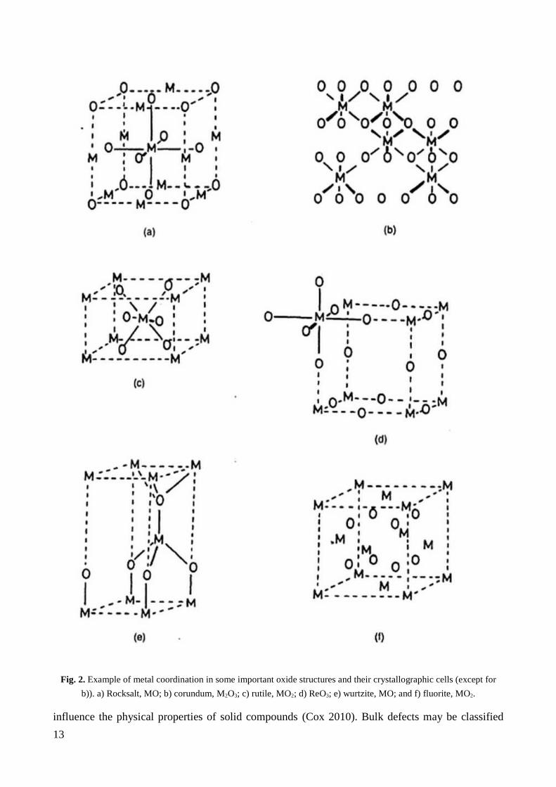
Fig. 2. Example of metal coordination in some important oxide structures and their crystallographic cells (except for
b)). a) Rocksalt, MO; b) corundum, M2O3; c) rutile, MO2; d) ReO3; e) wurtzite, MO; and f) fluorite, MO2.
influence the physical properties of solid compounds (Cox 2010). Bulk defects may be classified
13

either as extended defects, such as line (dislocations) or planar defects, as point defects, such as
lattice vacancies, interstitials or impurities and dopants occupying either substitutional or interstitial
states. Elementary theory of defects in ionic solids states that the occurrence of point defects is such
that there is a preservation of the overall charge neutrality of the solid. Thus we may have Frenkel
(vacancy plus interstitial of the same type) and Schottky (balancing pair of vacancies) types of
defects. Moreover, impurities may be associated with vacancies or interstitial sp as to balance the
overall charge: e.g., in Li-doped MgO, the substitution of Mg2+ by Li+ is compensated by an
appropriate number of O2- vacancies.
Electronic structure alteration at sites neighbouring to defects represents another important way by
with the charge balance is obtained. For example, the electrons remaining at an O2- vacancy may be
trapped at the vacancy sites to give F or F+ centres (Henrich and Cox 1994). Moreover, electrons
and holes may contribute to the oxidation states of a transition-metal ion. For example, oxygen
deficiency in TiO2 can be associated with electrons trapped at Ti4+ sites to give Ti3+, and oxygen
excess can increase the oxidation state of some atoms, as in Fe.0.9O, which may be considered to
have a proportion of Fe3+ ions in addition to Fe2+.
The strong influence of these defects on the electronic structure and properties of metal oxide, at the
base of thesis work dissertation, will be more in detail reported in the next chapters.
1.3 - Titanium oxide (TiO2) and zinc oxide (ZnO)
1.3.1 TiO2 research: motivations and applications
In these last years, research on titanium dioxide (TiO2) underwent to a great expansion process,
making this material one of the most studied among metal oxides. The interest in this wide band-
gap semiconductor is in principle due to the huge number of application it is suitable for, related
both to the development of novel devices and to the properties improvement of existing materials.
Worth mentioning is even the possibility of use it for several experimental techniques, starting from
its deposition, easily leading to well-defined crystals, to a focused modification of some of its basic
features (e.g. oxidation, surface reduction, etc.). Several tests performed in the years and a good
characterization of its general properties makes the titanium dioxide a good candidate for the study
of new physical or chemical phenomena.
As mentioned, TiO2 finds application in a huge range of fields, spanning from photocatalysis to
solar cells for the production of hydrogen and electric energy, from gas sensing to electronic
devices production. It is used very often as white pigment in paints and as corrosive-protection
coating, for bone implantations, as optical coating or in ceramics products. For a comprehensive
review of TiO2 surface science, applications and related topics, we refer to the excellent review
14

paper by U. Diebold (Diebold 2003), and briefly discuss here just a few among the most important
applications of this material.
Photocatalysis and photochemistry: Photocatalyst properties of TiO2 and its strong reactivity to
visible and ultraviolet (UV) light make it a perfect candidate for sunlight-based daily life
applications. Since the first studies carried out by Fujishima and Honda (Fujishima and Honda
1972) on the water photolysis on TiO2 electrodes, there have been major advances in the field of
TiO2-based photochemical decomposition (Henrich, Dresselhaus, and Zeiger 1976; Wei Jen Lo, Yip
Wah Chung, and Somorjai 1978; Lewerenz 1989). In the same framework we can also cite
applications of TiO2 in photo-assisted bio-degradation: interaction of oxygen or water with photo-
excited electrons and holes lead to the formation of reactive free radicals on the TiO2 surface of the
material: further interactions with organic species are thus easy to happen, resulting in their
decomposition into CO2 or H2O. These feature finds applications for purification in wastewaters
(Mills, Davies, and Worsley 1993), for bactericidal purpose (Maness et al. 1999), for the creation of
self-cleaning surfaces, as coating for car windshield (Paz et al. 1995) or even as coating of marbles
for preservation of statues and of manufactures of historical interest (Poulios et al. 1999). Another
important photochemistry application involves the medical photo-therapy, namely the cito-toxic
effects exerted on cancer cells by UV-activated slurry titanium dioxide injected under skin (Cai et
al. 1991; Fujishima et al. 1993; Sakai et al. 1995). For an extensive review on TiO2 photocatalysis
and photochemistry properties we recall to the work by Linsebigler et al. (Linsebigler, Lu, and
Yates 1995a).
Gas sensing applications: As previously mentioned (see previous section), many metal oxides are
used as active elements in common conductometric gas sensing devices, based on the measurement
of change in the conductivity of the system induced by gas adsorption. To this aim, most used
materials are ZnO and SnO2, but in recent years titanium dioxide is affirming a role as oxygen
sensor, e.g. in the control of air/fuel in car engines (Dutta et al. 1999; Xu et al. 1993; Kirner et al.
1990; GRANT 1959; Phillips and Barbano 1997; Campbell et al. 1999; Matsumoto et al. 2001;
Chambers et al. 2001; Garfunkel, Gusev, and Vul’ 1998). At high temperature, a large range of
oxygen partial pressures can be indeed be detected through chemoresistive transduction in
controlled bulk defects TiO2-based devices; addition of Pt, leading to the formation of Schottky
diode, is used to increase performances at low temperature (Kirner et al. 1990).
Electronics: Other motivations lying behind the interest in use of TiO2 regard the issue of novel
oxide gate materials (high-k oxides) substituting the SiO2 in MOSFETs (Garfunkel, Gusev, and
Vul’ 1998). Titanium dioxide represents an appealing candidate as gate dielectric, thanks to its high
dielectric constant and good possibility of control of its surface states and stoichiometry, represents
an appealing candidate for a new MOSFET generation (Garfunkel, Gusev, and Vul’ 1998).
Furthermore, has also some possible applications in spintronics (even if titanium dioxide is not
15

magnetic, it can exhibit ferromagnetic properties once doped with cobalt) (Matsumoto et al. 2001;
Chambers et al. 2001).
Biomedical applications: Finally, we mention the pigment and biomedical industry as another
application field of TiO2. Each year, there is a huge production of TiO2 pigments (almost 4-tons
(Kronos International 1996)) used for almost all typology of paints, thanks to its high refractive
index (Diebold 2003). Its atoxicity makes it often being found in pharmaceuticals and cosmetic
products (Hewitt 1999) and as food additive (Phillips and Barbano 1997). Biocompatibility of
titanium dioxide finds a fertile application source in the biomaterial and biomedical fields (Ratner et
al. 2004). Commonly used biomaterials, whose efficiency mostly depends on oxide layer chemical
and physical properties, are titanium dioxide-based (Sittig et al. 1999). An example on the oxide
contribution in bioimplants is given with in the work of Branemark, Kasemo and co-workers
(Lausmaa et al. 1987), in which corrosion resistance and support for Ti performance at tissue or
molecular levels, on osseointegrated oral and maxillofacial implants is ensured by the oxide layer.
1.3.2 ZnO research: motivations and applications
Thin films and nanostructures based on zinc oxide (ZnO) have been receiving a significant
attention, due to several intriguing physical and chemical properties exploitable for applications.
ZnO is a wide-bandgap non-centrosymmetric and piezoelectric n-type semiconductor, having a
direct bandgap of about 3.3 eV (room temperature). Thanks to the fact that direct gap structure
allows efficient electron-hole radiative recombination and thanks to its large exciton binding energy
(60 meV) exceeding the thermal energy (kBT), ZnO exhibits a stable and efficient
photoluminescence emission in the UV range even at room temperature (Özgür et al. 2005b).
Concerning its electrical properties, unintentionally doped ZnO behaves as n-type semiconductor
because of oxygen vacancies acting as electronic donor levels, similarly to the case of TiO2.
Apart from gas sensors (discussed more extensively next), many potential application of ZnO find
room at the intersection between electronics and opto-electronics, relying on both its conductive
properties, its piezoelectric properties and on its efficient room-temperature near-band-edge light
emission. For example, its properties make it suitable for realization of photodiodes (PD), metal-
insulator-semiconductor diodes (MIS), transparent conductive electrodes, piezoelectric devices for
energy harvesting.
In reference with the field of electronics and opto-electronics, ZnO is a promising material for
heterostructures realization and applications such as photodetectors (Jeong, Kim, and Im 2003; Ohta
et al. 2000; H. Ohta et al. 2003) and ultraviolet light emitting diodes (LEDs) (Alivov et al. 2003;
Ohta et al. 2000; Alivov et al. 2003, Drapak 1968). Moreover, ZnO has the advantage of being low
cost, non-toxic and easily grown on other p-type materials such as Si (Xiong et al. 2002; Jeong,
16

Kim, and Im 2003; Nikitin et al. 2003), GaN (Alivov et al. 2003; Yu et al. 2003), CdTe (Aranovich
et al. 2008), diamond (Cheng-Xin Wang et al. 2004) and NiO (Hiromichi Ohta et al. 2003).
Electroluminescence properties of ZnO are suitable for the development of metal-insulator-
semiconductor (MIS) diodes (Shimizu et al. 1978; Minami et al. 1974; Alivov et al. 2004).
Application of ZnO as transparent conductive electron is also important. Due to its wide bandgap,
ZnO is unreactive to visible light even under heavy-doping conditions. As discussed by Ozgur and
coauthors (Özgür et al. 2005b), 2*1021 cm-3 charge carriers can indeed be added without any lost in
its optical transparency in the visible range, making it a good candidate for applications in which
visible-light transparency is necessary (e.g. transparent electrodes in flat-panel displays, transistors
and solar cells).
Finally, applications based on piezoelectric properties of ZnO are of great importance to exploit
harvesting of mechanical energy from the environment (Wang and Song 2006). This characteristic,
integrated with the microelectronic or nanostructuring fabrication, can be employed in fields where
miniaturization coupled with smart powering conditions represents a promising way for the
development of non-invasive, environment-integrated and self-powered devices. Other examples
include wireless structures as biosensors, probes, scanning devices, etc power up simply exploiting
natural mechanical stress induced by blood flow, muscles stretching, mechanical vibration
generated by sonic or hydraulic waves and all similar daily life actions can be just few examples of
self-powered devices (Rusen Yang et al. 2009). At this purpose, different works were carried on the
use of nanostructured crystalline ZnO, thanks to its appealing piezoelectric and semiconductor
nature, biocompatibility and possibility of nanostructuring in various morphologies with really high
efforts (Xu et al. 2010).
1.3.3 Structural and electronic properties of TiO2 and ZnO
Titanium dioxide is a wide band-gap semiconductor naturally found in nature in three crystalline
phases: the most thermodynamically stable rutile and two polymorph metastable states, anatase and
brookite (Fig. 3). Phase transition are of course possible by heating the material: over 500°C,
anatase crystalline properties are obtained starting from amorphous titanium dioxide; slow and fast
brookite to anatase phase transformation are reached with respectively temperature below 780° and
between 780°C and 850°C; above this temperature, phase transformation to rutile occurs for both
anatase and brookite. Melting point and boiling temperature are respectively 1870°C and 2972°C.
In the following, a summary of the main characteristics of the titanium dioxide phases is discussed.
17
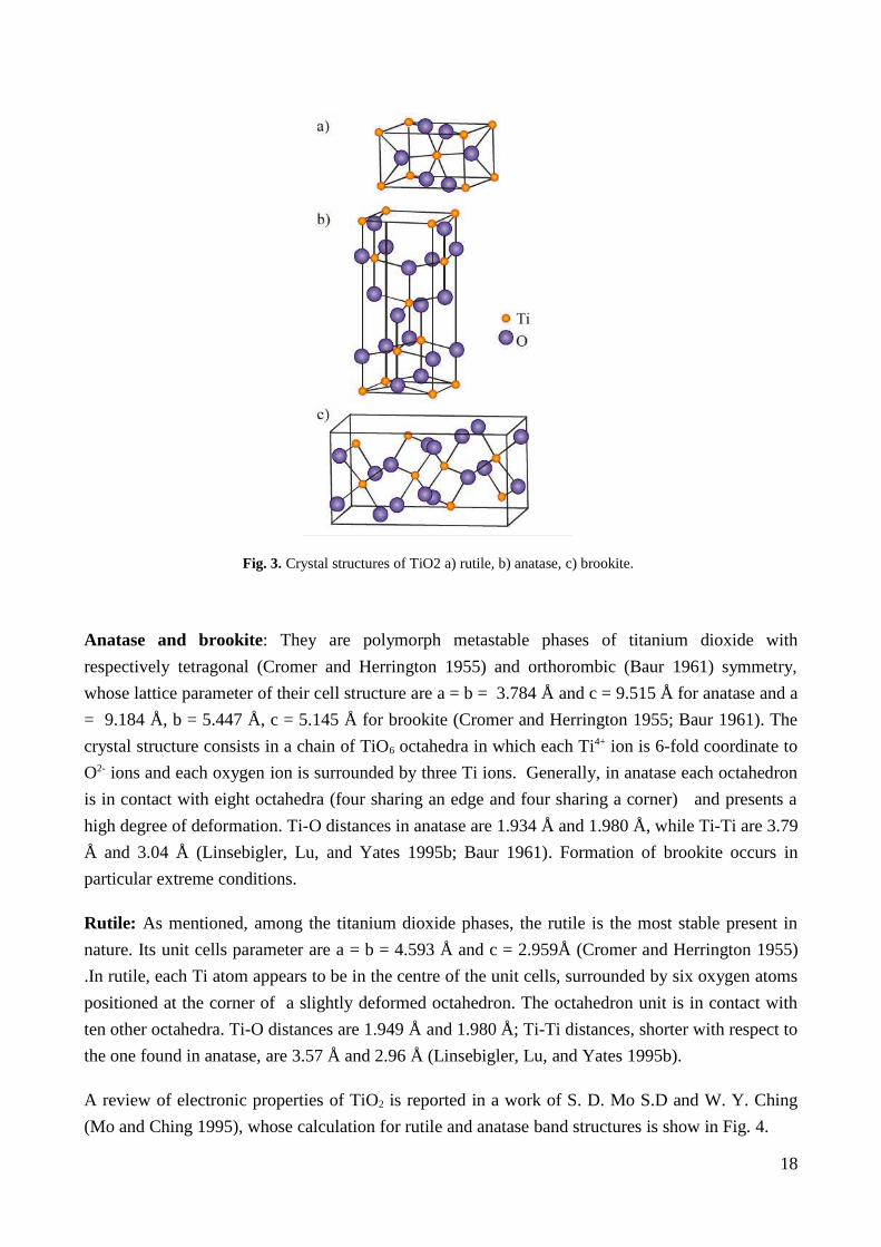
Fig. 3. Crystal structures of TiO2 a) rutile, b) anatase, c) brookite.
Anatase and brookite: They are polymorph metastable phases of titanium dioxide with
respectively tetragonal (Cromer and Herrington 1955) and orthorombic (Baur 1961) symmetry,
whose lattice parameter of their cell structure are a = b = 3.784 Å and c = 9.515 Å for anatase and a
= 9.184 Å, b = 5.447 Å, c = 5.145 Å for brookite (Cromer and Herrington 1955; Baur 1961). The
crystal structure consists in a chain of TiO6 octahedra in which each Ti4+ ion is 6-fold coordinate to
O2- ions and each oxygen ion is surrounded by three Ti ions. Generally, in anatase each octahedron
is in contact with eight octahedra (four sharing an edge and four sharing a corner) and presents a
high degree of deformation. Ti-O distances in anatase are 1.934 Å and 1.980 Å, while Ti-Ti are 3.79
Å and 3.04 Å (Linsebigler, Lu, and Yates 1995b; Baur 1961). Formation of brookite occurs in
particular extreme conditions.
Rutile: As mentioned, among the titanium dioxide phases, the rutile is the most stable present in
nature. Its unit cells parameter are a = b = 4.593 Å and c = 2.959Å (Cromer and Herrington 1955)
.In rutile, each Ti atom appears to be in the centre of the unit cells, surrounded by six oxygen atoms
positioned at the corner of a slightly deformed octahedron. The octahedron unit is in contact with
ten other octahedra. Ti-O distances are 1.949 Å and 1.980 Å; Ti-Ti distances, shorter with respect to
the one found in anatase, are 3.57 Å and 2.96 Å (Linsebigler, Lu, and Yates 1995b).
A review of electronic properties of TiO2 is reported in a work of S. D. Mo S.D and W. Y. Ching
(Mo and Ching 1995), whose calculation for rutile and anatase band structures is show in Fig. 4.
18

It is important to mention that calculated electronic energy distribution usually refer to ideal
structures. As mentioned in Sec. 1.2, real metal oxides exhibit intrinsic defects (vacancies,
interstitial atoms, dislocation, etc.) whose presence strongly affects the electronic levels and their
physical properties. An investigation on the energy distribution can be performed by means of
optical properties. PL spectroscopy, in particular, is a fruitful tool for studying the charge carrier
recombination and electronic spectrum, even though sometimes PL results are not of easy
interpretation. In TiO2 PL spectrum, for example, different emission bands are observed and a
univocal explanation for the chemical nature of energy level involved is still under construction.
The recurrent visible green emission in TiO2 NPs systems, is commonly attributed to both self-
trapped excitons (STE) recombination and defect states and surface radiative recombination
(Cavigli et al. 2009; Zhang, Zhang, and Yin 2000; Forss and Schubnell 1993; Bieber et al. 2007).
Defect states are moreover associated to intra-band levels leading to radiative recombination with
emitted wavelengths in the red region (Knorr, Zhang, and McHale 2007; Mercado et al. 2012)
Emission bands lying in the blue region (LIU et al. 2009; Maurya et al. 2011) of electromagnetic
spectrum and in the NIR (Montoncello et al. 2003; Knorr, Mercado, and McHale 2008) are
observed as well: even though different hypothesis have been proposed, the overall picture seems to
be not yet clarified. On this topic, a more detailed dissertation it will be reported in Ch. 5.
Fig. 4. Band. Band structures of a) rutile and b) anatase (adapted from (Mo and Ching 1995))
19

Zinc oxide is a wide band-gap semiconductor, whose ionic properties reside at the borderline
between ionic and covalent semiconductor, as for most of the to the II-VI group binary compounds.
It presents three crystal structures: wurtzite, zinc blend and rocksalt, schematically depicted in Fig.
5. At ambient conditions, wurtzite appears to be the thermodynamically stable phase, while it is
found that specific conditions are needed to obtain rocksalt and zinc blende phases.
Two comprenetrating hexagonal-close packed (hcp) sublattices compose the structure, showing a
displacement u = 0.375 between atoms of the same kind. Each sublattice is constituted by four
atoms per unit cell, in which each atom of one group results 4-fold coordinate, i.e. surrounded by
four atoms of the other group. Real ZnO crystals in wurtzite phase usually deviates from the ideal
form, showing different c/a ratio or u parameter value (Özgür et al. 2005b). Applying an external
hydrostatic pressure (starting with 9.1 GPa (Desgreniers 1998)) results in the phase change to
rocksalt (NaCl), thanks to the fact the reduced lattice dimensions favors ionicity over the covalent
nature thanks to interionic Coulomb interaction. Formation of the zinc blend structure is instead
obtained only growing the crystal by heteroepitexial growth on cubic substrates as ZnS (Kogure and
Bando 1993), GaAs/ZnS (Ashrafi et al. 2000) and Pt/Ti/SiO2/Si (Kim, Jeong, and Cho 2003)
reflecting topological compatibility to overcome the intrinsic tendency of forming a wurtzite phase.
Lattice parameters are summarized in Table 1.
Fig. 5. ZnO crystal structures. a) Hexagonal wurtzite structure; b) cubic zinc blende; and c) cubic rock salt. Biggest
spheres represent oxygen atoms, while Zn atoms are shown as smaller dark spheres.
20

Crystal structure Lattice constant Value Ref.
Wurtzite (hexagonal) a (Å) 3.2475-3.2501 (Noel et al. 2001; Catti,
Noel, and Dovesi 2003;
Karzel et al. 1996; Kisi
and Elcombe 1989;
Gerward and Olsen
1995)
c (Å) 5.2042-5.2075
u 0.383-0.3856
Zinc Blende (cubic) a (Å) 4.60-4.619 (Ashrafi et al. 2000;
Özgür et al. 2005b)
Rocksalt (cubic) a (Å) 4.271-4.294 (Recio et al. 1998; Bates,
White, and Roy 1962;
Recio, Pandey, and
Luaña 1993)
Table 1. Measured and calculated lattice constants and u parameter in ZnO.
A compendium of electronic band structure properties of ZnO is presented by Özgür et al. (Özgür et
al. 2005b), in which are reported several experimental studies and theoretical calculation of energy
level distribution for the three phases. A representative example of band structure calculation is
illustrated in Fig. 6, from a work of Vogel and coworkers (Vogel, Kruger, and Pollmann 1995),
where is clearly shown the direct band gap semiconductor nature of ZnO. This feature strongly
influences optical properties of ZnO, leading to the possibility of having excitonic recombination
(more details about interband recombination processes will be reported in Chapter 2). The
calculated band gap value is 3.77 eV, in agreement (Jagadish and Pearton 2006) with experimental
values. In real systems, intraband levels confer to ZnO an n-type nature. The nature of such shallow
states is usually attributed to zinc substitution by group-IV atoms (Al, Ga, In), while deep states are
usually attributed to intrinsic point defects, such as zinc interstitials and oxygen vacancies (Djurišić
et al. 2007a; Studenikin, Golego, and Cocivera 1998a) . A vast amount of literature deals with
identifying the chemical nature of interband energy levels and for further detail one can refer to
(Özgür et al. 2005a).
1.4 - Techniques for MOX thin films deposition
In the recent years, interests towards thin films increased more and more thanks to their versatility
and to the possibilities of controlling their properties, strictly depended on the growth conditions,
21

Fig. 6. a) LDA-calculated band structure of bulk wurtzite ZnO (Vogel, Kruger, and Pollmann 1995) b) Schematic
diagram representing the crystal-field and spin-orbit splitting of the valence band of ZnO into 3 sub-band states A, B
and C at 4.2 K. (Gun Hee Kim 2006)
that make them suitable active elements for applications in various and different fields (Martin
2010). The environment in which deposition takes place strongly effects on the structural and
morphological properties of thin films. Thus, a key role is played by all the controllable and tunable
growth parameters such as substrate temperature, kind and pressure of buffer gas, substrate nature,
time deposition and so on, and on their cause-effect relation on the properties of the deposited
product. For this reason, several deposition techniques have been developed, each of them able to
reach deposition of material with specific characteristic. Thin films deposition techniques can be
mainly divided in two groups: chemical and physical techniques. As the names suggests, on the
chemical category we can include all the techniques in which the deposition is based on chemical
processes. It is in turn divided in two subgroups, the so called gas-phase chemical deposition, such
as chemical and photochemical vapor deposition and thermal oxidation, and liquid-phase chemical
deposition, such as electrolytic deposition, electrolyitic anodizing, spray pyrolysis, solgel method,
hydrothermal and solvothermal methods.
In physical methods instead (e.g. sputtering or vacuum evaporation), the deposition takes place after
the material reaches the gaseous phase. This can be obtained in several ways: heating or local
energy absorption, causing material evaporation, may be done by means of particle collisions, as in
ionic beam deposition or sputtering, or by means of pulsed laser radiation, as in the pulsed laser
deposition technique (PLD). On this last method, used in this work, we will focus our attention with
a more detailed description of the technique and its applications.
1.4.1 Pulsed Laser Deposition
22

In the panorama of the depositions techniques, in these recent years laser ablation is becoming more
and more established thanks to its versatility in the production of nanostructures of a huge variety of
materials that find application in different fields of both fundamental research and technology
(Chrisey and Hubler 1994a; Miller and Haglund 1997). Laser ablation can be used for the
deposition of different materials as semiconductors, metals, dielectrics, organic and polymeric
products (some example are reported in Table 2, with relative references). Moreover, it can be
employed for the synthesis of structures, spanning from epitaxial to nanostructured or nanoparticles
films to lower-dimensional films, with several morphology, according to the deposition condition
chosen (Ashfold et al. 2004; Willmott and Huber 2000; Eason 2006; Chrisey and Hubler 1994b) .
Materials
Metals Al (Andreić, Aschke, and Kunze 2000), Cu (Mourzina et al.
2001), Fe (White and Scalapino 2000)
Semiconductors ZnO (Sun and Kwok 1999),TiO2 (Yamaki et al. 2002; Walczak
et al. 2008), nitrides (Z. M. Ren 1999; Szörényi et al. 2000)
Superconductors Yttrium barium copper oxide (YBCO) (Jackson and Palmer
1994), MgB2 (Mijatovic et al. 2004:2)
Biomaterials Glucose oxidase (GOD) enzyme (Phadke and Agarwal 1998),
silk fibroin (Tsuboi, Goto, and Itaya 2001)
Polymers Poly(methyl methacrylate) (PMMA), (Rebollar et al. 2006;
Blanchet and Fincher 1994), Poly(tetrafluorethylene)(PTFE)
(Inayoshi et al. 1996)
Table 2: Example of materials growth by PLD.
This process is based on the focusing of an energetic pulsed laser beam on a target in order local
heating causes evaporation of the material. that, so ablated, flights towards the substrate on which
the material is supposed to be deposited. All the process takes place in vacuum or in a controlled
atmosphere, in order to avoid contamination by external molecules and control stoichiometry of the
final product. That is why it can be considered has a “clean” technique, in which there is no extra
residual substance deposition, as can occur in chemical deposition techniques. The whole ablation
process can be divided in three stages:
- target interaction with laser and energy absorption:
23

According to the laser energy source, different scenarios are possible for this step.
Using a continuous wave laser leads to a “slow” absorption process involving both superficial
and bulk areas and generating an equilibrium thermal state for each of the component of the
material that will evaporate each of them according to their own melting point and vapor
pressure. The deposited material will thus result strongly under-stoichiometric. In case of pulsed
laser, the interaction time with the material is reduces and heating transport is limited to
superficial states: different target components reach thermal condition for evaporation
simultaneously. Not worth noticing the existence of a threshold limit for laser source above
which the ablation process can have place, dependent on laser characteristics and chemical-
physical properties of the material. When pulsed laser are used, it should be considered the
impulses rate: pulsed laser beam shorter than typical material response time (in the order of ns)
interacts both with the target and with the ejected material, while in the ultra-short pulsed laser
case (ps, fs regime), the interaction laser-material is limited to the target. Differences among this
two pulse regime will be shortly reported in the next section.
- plume formation and propagation:
Laser energy absorption induces very quick thermodynamic transformation in the material that
lead to its evaporation, with the creation of plasma, composed by electrons, ions, atoms,
nanometric clusters and molecules. Once the material is ejected, it propagates preferentially in
the direction orthogonal to the target surface, assuming a characteristic plume-like shape, from
which it takes its name. The dynamic of propagation of the plume in the vacuum chamber is
strongly effected by the environment atmosphere. In high vacuum condition, the plume keeps its
kinetic energy during the flight, while the presence of a buffer gas has a slow down of, with a
confinement of the material (the overall effects pressure-dependent will be analyzed in detail in
Chapter 4). Buffer gas role is, moreover, the preservation of stoichiometry of the material
deposited on the substrate or the addition of dopants.
- deposition on the substrate :
The last step is characterized by the deposition of ablated material on a substrate properly
chosen. Of course, the choice is first of all based on the purpose for which the nanostrucured
thin film is. Measurements of photoluminescence need, e.g., a substrate whose emission in the
range of excitation wavelengths of the material examined is negligible; for transmittance, a
transparent substrate for the region of electromagnetic spectrum of interest and so on. The
choice of substrate is, anyway, a more subtle topic since the growth of the films is effected by
the structural properties of the surface: an epitaxial growth of a thin film requires that the
substrate has a crystalline structure and similar lattice constants to the one of the deposited
material.
24

Thus, the ablation process and the resulting deposition can be effected by several parameters,
starting from the material and substrate chosen to the energy source adopted. Commonly, material is
ablated by means of pulsed laser with nanosecond pulse impulses (ns-PLD), (Eason 2006) used for
the controlled deposition of crystalline films starting from different materials. The temporal length
of the pulses, higher than typical responses of material, leads to interaction between laser beam and
formed plume during its propagation in near-target areas. Ejected material absorbs in turn laser
energy and the consequent temperature increasing causes an high degree of ionization and
atomization (Cremers and Radziemski 2006).
Fig. 6: Ns-PLD and laser interference with ejected plasma
Ns-PLD allow the growth of nanoparticles and nanoparticulated thin films ((Di Fonzo et al. 2009;
Aruta et al. 2010; Di Fonzo et al. 2008), in different morphologies, as showed in fig. 7 (Di Fonzo et
al. 2009). In this work, different dry air pressure in deposition chamber were used for the deposition
of titanium dioxide with 10-15 ns pulses generated by an eccimer laser (KrF, 248 nm) at 4 J/cm2
fluence: films, deposited at room temperature on silicon or titanium, show great variety of
morphologies, from compact to forrest-like.
25

Fig. 7. Different structures obtained with ns-PLD deposited at different pressure. a) 10 Pa; b) 20 Pa;
and c) 40 Pa.(Di Fonzo et al. 2009)
Recently, research is focusing on the use of shorter laser pulses and particularly interesting is the
regime of the femtoseconds. In this case, thanks to the short temporal duration of the pulses, energy
is transferred to the material in temporal scale less than the usual material time responses, thus
avoiding the extra interaction between ejected material and laser source occurring in the ns regime.
The high excavating state on which the material undergoes is characterized by high temperature and
inner pressure. In these physical conditions, relaxation processes out of equilibrium occurs for the
material, still under examination of researchers.
The fs-PLD allows the deposition of nanoparticles even in high vacuum conditions (Eliezer et al.
2004; Amoruso et al. 2004; Amoruso et al. 2005) and, up to now, this technique is mostly used for
the production of nanoparticles and nanoparticulated thin films from elementary (metals or
semiconductors) to simple compounds (metal alloys) (Nolte et al. 1997). Adoption of oxides as
target for fs ablation is instead still few investigated (Orgiani et al. 2010; Sambri et al. 2007) both
from theoretical and experimental point of view.
1.4.2 Pulsed laser ablation: theoretical model
Ultra-short pulsed laser ablation is a quite recent technique and up to now, a complete theoretical
support is still not been developed, in particular for complex systems as oxides. For the
femtosecond pulse regime, basic model commonly used for describing the transfer of energy from
pulsed laser radiation and material is the two-temperature model (TTM), for which the system is
approximated as composed by only two subsystem: the crystal lattice and the electron cluster, each
of them characterized by its own temperature, respectively indicated as Tl and Te. The electronic
subsystem acts as a bridge in the energy transferring between laser source and the material:
electrons, in fact, by means of vibrational lattice states (phonons) that transfer energy to crystal
lattice, according to the following expressions:
26
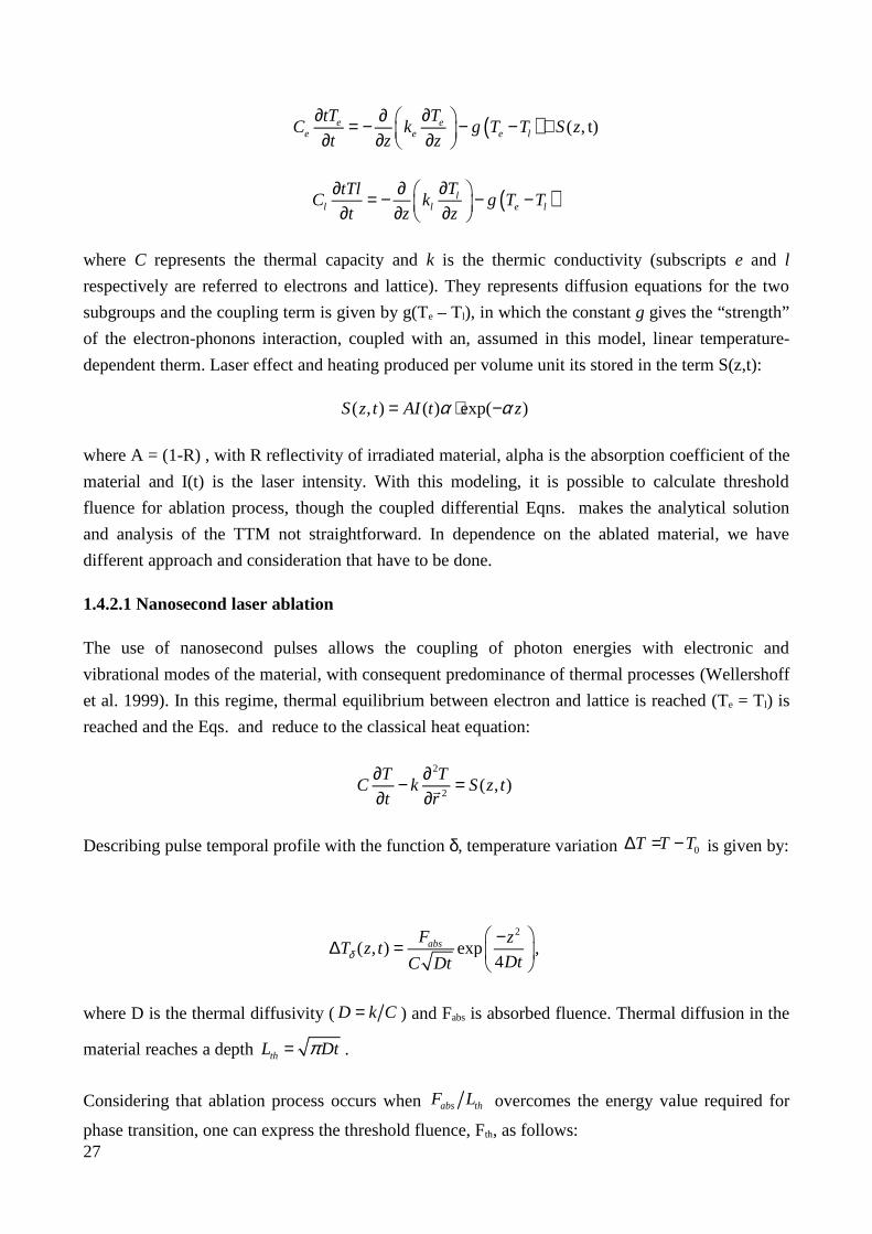
( ) ( , t)e ee e e l
tT TC k g T T S z
t z z
∂ ∂∂ = − − − + ∂ ∂ ∂
( )ll l e l
TtTlC k g T T
t z z
∂∂ ∂ = − − − ∂ ∂ ∂
where C represents the thermal capacity and k is the thermic conductivity (subscripts e and l
respectively are referred to electrons and lattice). They represents diffusion equations for the two
subgroups and the coupling term is given by g(Te – Tl), in which the constant g gives the “strength”
of the electron-phonons interaction, coupled with an, assumed in this model, linear temperature-
dependent therm. Laser effect and heating produced per volume unit its stored in the term S(z,t):
( , ) ( ) exp( )S z t AI t zα α= ⋅ −
where A = (1-R) , with R reflectivity of irradiated material, alpha is the absorption coefficient of the
material and I(t) is the laser intensity. With this modeling, it is possible to calculate threshold
fluence for ablation process, though the coupled differential Eqns. makes the analytical solution
and analysis of the TTM not straightforward. In dependence on the ablated material, we have
different approach and consideration that have to be done.
1.4.2.1 Nanosecond laser ablation
The use of nanosecond pulses allows the coupling of photon energies with electronic and
vibrational modes of the material, with consequent predominance of thermal processes (Wellershoff
et al. 1999). In this regime, thermal equilibrium between electron and lattice is reached (Te = Tl) is
reached and the Eqs. and reduce to the classical heat equation:
2
2( , )
T TC k S z t
t r
∂ ∂− =∂ ∂�
Describing pulse temporal profile with the function δ, temperature variation 0T T T∆ = − is given by:
2
( , ) exp ,4
absF zT z t
DtC Dtδ
−∆ =
where D is the thermal diffusivity (D k C= ) and Fabs is absorbed fluence. Thermal diffusion in the
material reaches a depth thL Dtπ= .
Considering that ablation process occurs when abs thF L overcomes the energy value required for
phase transition, one can express the threshold fluence, Fth, as follows:27

m thth
c T LF
A
ρ ∆=
In this expression, mT∆ is the difference between initial temperature and melting temperature of the
target, A represents the superficial absorbance and ρ the density of the material. From an energy
balance analysis, the material is melted and then vaporized up to a depth ∆zv given by:
(F F )thv
v
Az
Lρ−∆ ≈ ,
where vL represents the latent vaporization heat for mass unit. This diffusive process generates the
formation of a high pressure and temperature plasma. This strongly out-of-equilibrium system
evolves with the material from the target and the formation of an atomic and ions plasma plume.
Thermodynamic transformations occurring at target surface may lead to the formation and ejection
of nanometric or micrometrics (droplets) cluster, that may induce irregularity in the deposition
products. The ablation process occurs in a nanosecond-order temporal scale, when the laser pulse is
still impinging on the surface. Ablated material, during the formation and early propagation of the
plum, absorbs laser energy, inducing an additional plasma ionization or, for high fluences, a shield
effect with respect to the target surface (Amoruso 1999; Ihlemann et al. 1995)
Plume atoms and ions disexcitation occurs via radiative processes, too, thus giving the possibility
of carrying on spectrographic analysis on the plume for the determination of its components and
their distribution in it, a part that, of course, the possibility of visualizing it, for example by means
of an ICCD (intensified charged coupled device). Plume has propagation direction preferentially
orthogonal to target surface, an ellipsoidal profile (Anisimov, Luk’yanchuk, and Luches 1996) and
is formed by about 1015 particles per laser pulse, with a Maxwell distribution of velocity:
23 ( )
( ) exp2
m v vP v v
kT
− −
∼ ,
where v and v are, respectively, velocity (orthogonally oriented with respect to target surface) of a
particle and of the plume mass centre; average mean velocity in vacuum is, generally, 610 cm s∼
(Walczak 2010).
1.4.2.2 Femtosecond laser ablation
This regime is characterized by pulses whose duration is shorter than energy transfer time from
electron to the lattice. For this reason, in the equations and is not possible to neglect the electron-28

phonon interaction term: laser energy is transferred first to the electrons and from them to the
lattice, as an inner heating source. The analysis of the process is easier for the case of metals,
described in the following and adapted to the semiconductor case of our interest.
Basically, the idea is to, separately, analyze the electronic and the lattice equations, since the two
systems are characterized by different characteristic times (Amoruso et al. 2005). One can
demonstrate that ablation takes place when laser fluence overcomes limit fluence of vaporization
Fth, whose expression is (Wellershoff et al. 1999):
th
LF
Aνρ
α=
where ρ is the material density, Lν vaporization latent heat per mass unit,, α the absorption
coefficient and A is the superficial absorbance. Nolte et al. (Nolte et al. 1997) proposed for the
TTM equations a solution that links the laser fluence with the ablation depth ∆L due to the laser:
lnth
FL
Fδδ∆ ≈ ⋅
where F F and thF δ are respectively absorbed and optical limit fluence (δ is the optical penetration
length). If thF F δ≫ , the thermal regime is established for the system, whose electron transfer energy
overcomes characteristic optical penetration δ. In such regime, ∆L becomes:
lnl
th
FL l
F∆ ≈ ⋅
in which lthF indicate limit fluence for thermal regime and l is the electrons thermal penetration
length (Nolte et al. 1997).
In semiconductor and dielectric materials, absorption is due to two phenomena: avalance ionization
and multiphotonic ionization. The first is a step process consisting in the subsequent ionization of
atoms by means of high energy electrons: laser absorption can transfer an amount of energy to
electrons enough to cause an avalanche process in which free electrons can transfer energy to bound
state carriers that in turn will induce ionization processes. This mechanism it is assumed to be
dependent to the free electrons density and be proportional to laser intensity (Grigoropoulos 2009).
The multiphoton ionization occurs when the material band gap is higher then the energy of incident
photons: in this circumstance, in fact, a single photon is not able to transfer enough energy to create
an electron in the conduction band. In multiphoton transition, N photon of energy hν are “view” and
absorbed by the material as a single photon with energy Nhν: in this way, it can ensure the initial
creation of carriers necessary for the verifying of ablation process. In large band gap semiconductor,
29

for high laser intensity (>1013 W/cm2), as for typical fs pulsed laser, ablation occurs only by means
of multiphoton ionization. For higher band gap materials, other phenomena occurs, as coulombian
explosion, negligible for metals and semiconductors. A schematic representation of both the
processes is shown in Fig. 8.
Fig. 8. Absorption due to avalanche ionization and multiphoton ionization.
In the TTM for semiconductors and dielectric, have to be introduced a differentiation for the
coupling between electron and phonons: lattice-electron interaction promote the increasing of
optical phonons, thus preserving the validity of the TTM as described before, with a thermal
equilibrium reached for times in the order of 10 ps. In the parameter S Eq. , a non-linear photon
absorption contribution and a time dependency for the coefficient A since absorption varies by time
as electrons are created in the conduction band due the ionization processes at the base of ablation
(Grigoropoulos 2009; Bulgakova et al. 2004). However, the strong localization of interaction with
laser in ultra-short time and the high efficiency in the generation of the carrier makes scale time of
thermal relaxation for semiconductors and metal time comparable.
Irradiation and heating by laser energy absorption is, of course, only the very initial part of the more
complicate ablation process. Only considering the ultrashort material thermalization time (in the
order of ps) is not enough for explaining the expansion of the material, that occurs when a proper
pressure gradient is established in the irradiated material with respect to the external environment.
Irradiation absorption causes the formation of a supercritic fluid (with density of the order of solid
density) at a temperature radiation-dependent. Perez and Lewis (Perez andLewis 2002) proposed a
model for the description of the whole ablation mechanics, starting from the supercritic fluid and
following its dynamic that leads to the formation and expansion of the plume. For this latter, by
means of a Lennard-Jones bidimensional potential, it is obtained the phase diagram of temperature
in function of material density (Fig. 9) and it is found plasma forms and evolves according to a
four-steps mechanism: spallation, phase explosion, fragmentation and vaporization.
The spallation occurs when absorbed energy is near to threshold energy: heating the material over
the critical point (CP) at constant pressure leads to its relaxation towards the solid state following
the phase-coexistence areas but, increasing the energy of the systems, this relaxation cab bring the30

material to the liquid-gas phase passing to the bimodal curve that links the critical point with the
triple point. In this condition, fusion of the system takes place with formation of vapor bubble: if
this transition phase is fast, it can end with the phase explosion. Fragmentation occurs when elastic
energy stored by the material is equal superficial energy of the ideal isolated system: in this
situation, a fragmentation of the material occurs with the formation of little conglomerates. When
laser energy is enough high to make superficial states reach atomization, the vaporization process
starts, being the correspondent thermodynamic curves far from the liquid-gas coexistence curve. In
the fs ablation regime, a little amount of the material is in micrometric clusters (Amoruso, Vitiello,
and Wang 2005).
Fig. 9. Phase diagram (T,ρ). S represent solid phase, L is the liquid phase and V, the gas phase. CP
and TP are respectively the critical point and triple point. Lines 1-3 indicate adiabatich path given
certain initial condition for temperature and density (T0,ρ0)
Chapter 2
31

Opto-chemical approach to gas sensing
based on photoluminescence transduction
in metal oxide systems
The original research work discussed in the present dissertation regards the study of the
photoluminescence (PL) response to adsorption of oxidizing molecules in some specific metal
oxides. Aim of the present chapter is to provide the basic knowledge necessary to motivate and
discuss such approach to gas sensing. Therefore, I introduce here the topic of photoluminescence
phenomena in semiconductors, also depicting some basic and phenomenological modeling capable
to approach the issue of photoluminescence quenching caused by adsorption of oxidizing molecules
on surfaces of light-emitting oxides.
To be more precise, in the first section I will present an introduction to the photoluminescence
phenomenon in semiconductors i.e. a radiative de-excitation process occurring in a material excited
by means of light stimulus. An overview of the main physical origin of photoluminescence process
is also reported (interband transitions, exciton transitions, defect states transitions).
Photoluminescence process plays an important role in probing of quantum-mechanical electronic
states of a material, since the photon emission is strictly material-specific, and can even give a
general sight on its main structural and morphological properties.
In presence of adsorbed gas molecules, PL emission may undergo to modulation, caused by change
in the density of excited states and/or by a change in the radiative recombination probability. The
second section is devoted to a phenomenological modelling of the gas- induced PL modulation. In
particular, it will be shown the difference relying in the two processes at the base of PL variation,
presenting the concept of static and dynamic quenching. With the support of the Langmuir theory, it
will be found an explicit correlation between PL modulation and ambient gas pressure.
Experimental literature studies supporting the described modelling will be reported in section 2.3.
2.1 – Photoluminescence: an overview
32

When interaction between a material and an external energy source occurs, different excitation
processes can take place, leading to the creation of excited, unstable states. Restoring of the ground
state condition can be reached through several decay channels: when a radiative disexcitation
process occurs, i.e. the energy is released via emission of photons, we are in presence of the so
called luminescence phenomena. According to the typology of the external exciting source, we can
define several kind of luminescence: for instance, we can distinguish between thermoluminescence
(excitation obtained heating the system), chemiluminescence (in which chemical reaction is the
active exciting source), electroluminescence (electric current-induced) or photoluminescence (with
excitation process obtained irradiating the material). Generally speaking, this kind of processes
plays an important role in probing of quantum-mechanical electronic states of a material, since the
photon emission is strictly material-specific, and, as it will be explained in the next chapters, can
even give a general sight on its main structural and morphological properties. An emitted photon
with wavelength λ, in fact, has an energy E (given by the formula E = hc/ λ) whose value
correspond to the energy gap between the excited state level and the ground state level: it is thus
clear that analyzing the luminescence spectra can give precise information on the energy
distribution levels in the material. Moreover, since the luminescence can occur until the external
source is active and/or the excited state exists, isolating the system immediately after excitation
allow the examination of decay kinetics and excited state lifetime.
From now on, the attention will be focus only on the photoluminescence process, with a more
detailed overview on basic theoretical statements and on its importance as probing means in the
analysis of optical properties of materials. In particular, this process includes the fluorescence, with
its photon emission within 100 ms from excitation, and the phosphorescence, for which the
emission occurs after 10-5 s.
In the photoluminescence (PL), as previously mentioned, the excitation of a material due to
absorption of electromagnetic radiation leads to the creation of excited stated, whose radiative
decay gives place to emission of light. For a semiconductor, this process is actuated with the
recombination of photoexcited electron-hole pairs, with a release of energy dependent on the energy
level position of the two carriers involved in the process and can be supposed as compound by three
main steps:
excitation :consists in the electromagnetic radiation adsorption and electron-hole couples
generation. In first approximation, it can be considered as an instantaneous process;
thermalization: the system reaches thermodynamic equilibrium by carriers-carriers and phonon-
carriers interaction: n this step, carriers reach the edge of the respective band. Its duration is from
some tenths of femtoseconds to some picoseconds, depending on the carrier density;
recombination: radiative process due to ground state relaxation of carriers.
33

Since the photoluminescence emission is strictly correlated to the energy distribution of the
material, it is clear the extreme importance of having knowledge about the contributors to PL
spectrum, both for an optical characterization of the material and for eventual applications in
macroscopic mechanical devices. Briefly in the next they will be reported the typical main active
PL center.
2.1.1 Interband transitions
In a semiconductor single crystal, the described photo-excitation process with creation of electron-
hole in the respective band by irradiation is possible only by absorption of “over-band gap energy”
photons, since, by definition, in the band-gap region no available state for the carrier exists.
Moreover, simple considerations on lifetimes allow assuming as active elements for the
recombination mostly thermalized charged carriers, distributed along the edges of their respective
band giving a radiative emission with near the band gap energy. In real systems, additional levels in
the energy distribution, as effect of the presence of defect states, just introduce extra decay
channels, but is reasonable to expect that interband transitions are the main contributors to the PL
emission. It is worth noting how the conversation of crystalline momentum plays a crucial role in
this process. In particular, very strong radiative emission is usually observed in direct gap
semiconductors, while much smaller light emission efficiency are observed in indirect gap
semiconductors. Such difference lies in the momentum conservation principle, that leads to fact that
only “vertical” inter-band optical transition (i.e. preserving the crystalline momentum) are allowed
due to electron-phonon interactions. In indirect gap semiconductor, the inter-band transition it is
necessary the assistance of a phonon providing for the crystalline momentum difference of
thermalized charge carriers. Generally, the greater is the number of involved particles in a process,
the less is the probability it happens: this explain the difference between direct and indirect gap
semiconductor emission, with the further PL interband emission weaker then for the direct one.
Few considerations easily allow obtaining an approximate expression of PL intensity emission for
direct gap (the indirect gap PL expression is omitted being just a generalization of the simplest
direct gap case). For each photon energy hν, PL line is proportional to the number of states per unit
volume with energy difference ∆E equal to hν, i.e. the joint density of states (DOS) for the system,
and to a temperature-dependent factor taking into account the effect of temperature in the
occupation number of states. These simple considerations thus obtaining in total:
1 2( ) exp[ ( ) / for ( )
0 otherwiseg g B g
PL
E E k T EI
ω ω ωω − − − ≥
∝
ℏ ℏ ℏℏ
34

where a Boltzmann factor is used to take into account the temperature influence on the electrons
and holes populations.
The temperature parameter appearing in the above expression is related on the statistical thermal
distribution of charge carriers and not has to be confused with the lattice temperature, describing
instead the vibrational state of the crystal and its phonon distribution. Electrons and holes
temperature can reach higher values than that of the crystal lattice when high intensity source
excites the system. Photoluminescence is indeed one of the few methods allowing a direct
determination of carrier temperature (Yu and Welber 1978).
2.1.2 Exciton transitions
An effect that should be taken into account in presence of real crystal is the possibility of Coulomb
interaction between electrons and holes, that brings to the formation of bond states, the so called
excitons, a bosonic quasiparticle that, in turn, can exist as a free or localized state, generating from
the interaction with atoms in the periodic structure. Formation and lifetime of excitonic states is
strongly dependent on the temperature of the system: thermal motion of electrons and holes, in fact,
affects the binding that results to be broken if the excitonic binding energy is less than the
Boltzmann thermal energy kBT. The presence of excitons influence in the PL spectra results in
shifted emission lines, that differs from near- band edge emission for a value equal to exciton
binding energy, where the “missing” energy amount corresponds to the energy necessary to break
the electron-hole binding. Once the charge carriers are decoupled, they recombine as previously
described. Thus, this temperature dependent emission is more evident at low temperature, when
thermal vibration is less effective even if in some material, as ZnO, it is strongly evident even at
room temperature, being binding energy very high.
2.1.3 Defect states transitions
In this last category can be grouped all that defect states causing the loss of the periodicity in the
atomic configuration of a real crystal such as atom vacancies or substitutions, interstitial atoms,
dislocations, extrinsic doping, etcetera. Crystal defects, in fact, can act as traps for electrons and
holes causing, in terms of energy distribution, the availability of extra energy levels, situated in the
“forbidden” intergap region found starting with the Block theorem for a perfect crystal. PL emission
generated from these occupied states results peaked at energy values well below the band gap.
Defect states radiative emission are observed in PL spectra of many transparent conductive oxides
in which, moreover, these deep states very often are associated with surface sites, thus making
encouraging studies on the possible use of them as active element in PL-based gas sensor devices.
2.2 - Phenomenological modeling for gas-induced PL quenching
35

Under a given and constant stimulus (i.e. laser excitation), the total intensity (i.e. number of emitted
photons) of photoluminescence emission spectrum depends on the number of excited states (i.e.
photoexcited electrons and holes) provided by the excitation source times the probability associated
to a radiative recombination. Therefore, it is quite intuitive that any eventual modulation of
photoluminescence intensity caused by gas adsorption may arise mainly due to two reasons: a) an
increase/decrease of the density of excited states, and/or: b) a change in the radiative recombination
probability.
In the present section, I will illustrate a phenomenological modeling capable to describe these two
latter effects, also introducing some useful concepts such as the “dynamic” vs. “static” quenching
mechanism. The modeling relies on the use of a simple two-level system to approach the issue of
the correlation between the PL intensity modulation and the external partial pressure of the gas to
which the material surface is exposed.
One of the advantages of the following approach is in not requiring to specify the actual chemical
nature of states contributing to PL emission, that are simply referred as light-emitting centers (LEC)
and existing only in two states (i.e. two-level model), namely the fundamental state X and an
excited state X*. In such a scheme, PL intensity, given by the total number of radiative transitions
taking place after excitation, depends on the probability that such emitting processes occur and on
the density of involved states (indicated as [X] and [X*]). As already mentioned, when the material
is inserted in a non-inert atmosphere, gas adsorption can affect both the probability of radiative
recombination and the number of available emitting states. The two cases characterize the dynamic
and the static quenching, respectively.
2.2.1 Dynamic quenching of PL intensity
We consider here a two-level system interacting with the environment only by photon absorption
and assume that both radiative and non-radiative recombination pathways are available for the
decay of the excited state (X*) toward the fundamental state (X).
Here we assume that the presence of gas molecules adsorbed at material surface and acting as a PL
quencher induces the occurrence of an additional non-radiative recombination path, thus reducing
the probability for radiative emission and, in turn, the PL intensity.
Under such hypotheses, the possible processes involving X and X* states are shown below:
Excitation: *I
X h Xωα
ω+ →
Radiative recombination: * 'rk
X X ω→ + ℏ
36

Non-radiative recombination: *nrk
nrX X Eδ→ +
Quenching: * *qk
adsX Q X Q+ → +
The above expressions indicate that the absorption of laser photons (whose energy is energyωℏ ,
see Eq., creates excited states X*, which can undergo to different transitions towards the
fundamental state X. Recombination processes are represented by: emission of photoluminescence
photons (whose energy in ωℏ , see Eq. ); non-radiative processes (with exchange of a certain energy
δEnr with the crystal lattice, Eq.) or though energy exchange with adsorbed gas molecules (Eq. ). To
each of the four processes is associated a recombination rate W, defined as the number of processes
having place per unit volume and time. It depends on the density of states [X] and [X*] by means of
coupling constants (kr, krn, kads), and their expression is:
Excitation rate: [ ]excW I Xω ωα=
Radiative recombination rate: [ *]PL rW k X=
Non-radiative recombination rate: [ *]nr nrW k X=
Quenching rate: [ *][Q ]Q q adsW k X=
Here, Iω and ωα represent the intensity of light source (laser) and absorption coefficient at laser
photon energy 'ωℏ (respectively); [Qads] is the density of quencher adsorbed on the material (in
principle this density differs from the one of environmental gas), and [X] ([X*]) is the density of
fundamental (excited) states.
To obtain the expression for the PL intensity obtained under continuous-wave (CW) excitation (i.e.
“continuous wave photoluminescence” or CWPL), it is useful to calculate the recombination rates
for [X] and [X*]. In fact, the emitted radiation intensity is proportional to the number of radiative
transition per unit-time which, for CWPL, depends on the value of the recombination rate at steady
state. Assuming that no other processes are involved in the transition processes except those
reported in Eqs. to , we obtain
([ ] [ *]) 0d
X Xdt
+ = and [ ] [ *] 0SS SS
d dX X
dt dt= = ), valid for excitation provided by a stationary
source (as for a continuous-laser in CWPL), starting with a manipulation of expressions - leading
to:
37

[ ]( [ ])[ *] [ ]PL NR Q exc r nr q ads
d XW W W W k k k Q X I X
dt αα= + + − = + + −
[ *] [ ]( )PL NR Q exc
d X d XW W W W
dt dt= − = − + + + ,
Imposing now the steady-state conditions by the position *[ ] [ ] 0SS SSd X dt d X dt= = and considering
firstly the case in which the quencher is absent ([Qads] =0), we obtain:
[ *] [ ]0 ( )[ *] [ ] 0 [ *] , ss ss
r nr ss ss ss D r nrD
d X I Xk k X I X X k k k
dt kω
ωαα= ⇔ − + + = ⇔ = ≡ +
Recalling that the photoluminescence intensity (emitted photon flux Φ) is proportional (apart from
unessential geometrical factors) to the radiative recombination rate Wr (i.e. the number of photons
emitted per unit time and volume), the following expression is obtained:
0 [ ][ ] ss
PL r ss rD
I Xk X k
kωαΦ = =
where 0PLΦ represents the PL emission intensity when no gas (or just inert gas) interacts with the
material ([Qads]=0). The previous expression indicates that the total yield of emitted photons
depends on the excitation intensity adsorbed by the material ( Iωα ), on the density of available
LECs ([X]ss) and on the probability associated to radiative recombination, represented by the
internal radiative quantum efficiency ( )r r nrk k k+ .
Adding an additional recombination channel related to gas adsorption ([Qads] ≠ 0) we obtain:
[ *] [ ]0 [ *] [ ] [X*] [ ] 0 [ *]
[ ]ss ss
D ss ss q ss ads ssD q ads
d X I Xk X I X k Q X
dt k k Qω
ωαα= ⇔ − + − = ⇔ =
+ ,
and thus:
[ ][ ] [ ] rPL r ss ss
D q ads
kk X I X
k k QωαΦ = =+
The role played by the gas adsorption in modifying the PL intensity is now clarified. In fact, in the
developing of all the previous expressions, we assumed that the steady-state density of emitting
centers [X]SS is not changed by presence of a quencher, while this latter affects the PL process only
by adding as additional recombination term associated to a coupling constant kq.
The ratio between PL emission intensity in inert ambient and in presence of the quencher is given
by: 38

0 1 [ ]qads
D
kQ
k
Φ = +Φ
Thus, we see that in order to obtain a functional law linking the PL quenching and the external
(partial) pressure of the gas analyte we need to link this latter to the surface density of adsorbed
molecules [Qads]. To this aim, a quite general expression can be provided by the Langmuir formula
that will be treated in the next sections. The Langmuir model assumes a maximum possible density
of adsorbed molecules, or in other words a finite surface density of available adsorption sites. We
indicate this latter by Q0. Introducing the coverage θ as the fraction of occupied quenchable sites
(i.e. θ = [Qads]/[Q0]), we have:
0 1 Q
D
k
kθΦ = +
Φ
where [ ]0Q qk k Q= ⋅ . This expression shows that variations of photoluminescence emission can be
expressed by determining the surface coverage on the material when a gas is introduced in the
ambient atmosphere. The issue of determining the surface coverage vs. external gas pressure is
discussed in section 2.3.
2.2.2 Static quenching of PL intensity
Adsorption of gas molecules acting as PL quencher can lead to a different scenery with respect to
the simple introduction of extra recombination channel (that was the subject of the previous
section). In fact, modifications on electronic energy spectrum and on properties of electronic states
can be introduced by chemical interactions between material and adsorbed species. In this case, we
are in presence of the so-called “static quenching” mechanism, whose differentiation with respect to
the dynamic quenching is the changing in the density of LEC due to gas-material interaction. A
simple modeling is obtained starting from the Eqs. -, since all possible recombination paths for
excited carriers are exactly the same as in the case of the dynamic quenching process in absence of
gas interaction. From calculation previously reported, we have:
0[ ][ *] ; [ ] [ ]ss r
ss PL r ss ssD D
I X kX k X I X
k kω
ωα α= Φ = =
In the above expression we now introduce the dependence between LEC and adsorbed quencher
densities. In first approximation, one can assume a linear proportionality between them, obtaining,
despite to the simplicity of the expression, results comparable with real material behaviour (see
section 3 for some literature examples). We can thus define:
0 0[ ] ( ) [ ] (1 '[Q ]) [ ] (1 )ss ss ads ssX Q X Xβ βθ= − = −
39

where [X]ss is LEC density in absence of quenchers, [Qads] is the concentration of adsorbed species
and β = β’[Q 0 ] is a proportionality constant. In this expression, again the total coverage is
considered a fixed, material-dependent parameter. On balance, ratio of PL emissions is now
expressed by:
0 1
1 αθΦ =Φ −
Some considerations are now needed for a better comprehension of the whole mechanism.
First, we underline that unless a link is given between the coverage and the external gas pressure
(which the controllable experimental parameter), real experimental results can hardly be handled.
For this aim, in the next section (2.3) it will be reported the adsorption process model proposed by
Irving Langmuir.
Secondly, we consider the expression reported in Eq.. It is clear that its validity is ensured only for
values of βθ less than unity (an “over-coverage” surface is not considered as possible in the
development of this basic theory). Thus, from series expansion 0Φ Φ :
20
1
( ) 1 ( ) ... ( ) ...n n
n
αθ αθ αθ αθ∞
=
Φ = = + + + + +Φ ∑
we can see that for small values of αθ ( 1αθ ≪ ) it reduces to the following expression:
0 1 αθΦ ≅ +Φ
A comparison between and shows that they share the same functional form, that can be referred as
“proportional quenching” (due to the direct proportionality with the coverage). In other words,
static PL experiments alone may not allow distinguishing between static and dynamic quenching
mechanisms. To obtain further insight, we should rely on additional analyses. In particular, we will
discuss in section 2.4 about the importance of time-resolved PL experiments to obtain a clear
insight in the physical processes underlying the PL quenching phenomena.
2.2.3 Surface coverage in Langmuir theory
Langmuir theory allows obtaining an explicit link between the surface coverage and the external
(partial) gas pressure. The statements on which this model is based are the following ones:
40

• adsorption of molecules takes place on specific superficial fixed sites,, indistinguishable to
each other from energy point of view;
• on each site only one molecule at a time can be associated;
• the same desorption enthalpy is associated to each site;
• atoms and adatoms translation on the surface or into the material is not allowed (monolayer-
adsorption).
With these assumptions, it is possible to obtain an expression (Boer 1953; Hudson 1998) linking
surface coverage (θ) and partial pressure (P) of ambient gas molecules:
(P)1
bP
bPθ =
+
where b is a temperature dependent parameter given by:
01 2
0
1exp
(2 )des
B B
Hb
Q mk T k T
τπ
∆=
In which τ0 is the mean lifetime of adatom in the limit of high temperatures and ∆Hdes is the
desorption enthalpy (Hudson 1998).
With these findings, we can thus obtain an expression that quantifies dynamic and static quenching
in function of external partial pressure P of quenching gas molecules:
0 ("dynamic quenching") 1 (1 )Q
D
k bP
k bP
⋅Φ = +Φ +
0 ("static quenching")1
1 (1 )
bP
bPαΦ +=Φ + −
We have thus obtained a desired expression for the coverage, linking it to the experimental
parameter (i.e. the external gas pressure) that is typically measured and controlled.
Again, we can see that in the low pressure limit both expressions reduce to a linear “proportional
quenching” regime. In the limit of 1bP≪ (i.e. bPθ ≈ ), Eq. leads the Stern-Volmer equation:
0 1 1Q
D eff
k b PP
k P
⋅ Φ = + = + Φ ,
where effP acts as an “equivalent pressure” parameter that quantifies the effect of gas molecules at
41

given pressure P. In case of low pressure effP P≪ we have for the Stern-Volmer equation
0 [1 ( )]effP PΦ = Φ ⋅ − , in which is evident a linearly proportional dependence of the
photoluminescence emission with respect to the external gas pressure. The same trend can be
obtained for the static quenching case, for which in the limit 1bP≪ we have
0 0(1 ) (1 )bPαθ αΦ = Φ ⋅ − ≅ Φ − .
Results obtained up to now on the influence of adsorbed quenching species are summarized in
Table 3.
Type “Dynamic” “Static”
Quenching mechanism Quencher introduces additional non-
radiative recombination channels
Quencher modifies the number of
available emitting centers
PL intensity ratio vs
quencher coverage
0 1 Q
D
k
kθΦ = +
Φ 0 1
1 αθΦ =Φ −
PL intensity using
Langmuir model0
1( )
1 (a )
bPP
b P
+Φ = Φ ⋅+ + 0( ) 1
1
bPP
bP
α Φ = Φ − +
Table 3: Summary of static vs dynamic quenching results.
2.2.4 Importance of time-resolved photoluminescence analysis
As demonstrated previously, static and dynamic quenching mechanisms can lead to the same
functional law of quenching ratio vs. external gas pressure in cases where the modulation is not
large. In order to distinguish between these two cases, time-resolved photoluminescence technique
is of great help. In fact, the real difference between the two is the presence or not of an additional
non radiative decay channel, resulting in the change or recombination lifetimes. From equation -,
we have in fact for the total rate equation:
[ ][ *] (k [ ]) *PL nr Q D q adsd X dt W W W k Q X− = + + = +
Considering that total PL emission is proportional to the radiative rate integrated over time, one
obtains for the PL yield:
42

*0 0[ *] exp( ) [ ]r t r tk X t dt k Xτ τ= =Φ ∝ − =∫ ,
and, consequently, 0 0τ τ = Φ Φ , where τ and Φ are respectively the effective recombination
lifetime and PL yield (the subscript differentiate presence and absence of quencher cases).
Moreover, remembering Eq. , one can write the following Stern-Volmer expression (Stern and
Volmer, 1919)
0 01 [Q ]q adskτ τ τ= +
Adatoms density affecting on the probability of radiative decay thus results in changing the
recombination lifetime. Clearly, such a result does not occur in case of a mere reduction of LEC
density, characterizing the static quenching. Thus, analysis of TRPL can be of crucial importance
for distinguishing the dominant process at the base of photoluminescence quenching.
2.3 - Some literature examples of gas-induced PL modulation in oxide systems
Among metal oxides, tin dioxide (SnO2) is probably the most employed material for gas sensing
applications. SnO2 is a wide-bandgap n-type semiconductor that generally finds application in
several fields, such as catalyst support, dye-based solar cells and transparent electrodes. Moreover,
its chemoresistive responses strongly encouraged its use in conductometric gas sensors, up to being
nowadays one of the most exploited materials in this area. The possibility of growing quasi-1D
SnO2 structures, with well-defined single crystal surface (Dai et al. 2002; Liu, Dong, and Liu 2004;
C. F. Wang et al. 2004; Ramgir, Mulla, and Vijayamohanan 2004) boosted the interest in testing
and studying such single-crystal structures as active gas-sensitive elements.
Quasi-1D single-crystal SnO2 nanostructures exhibit a PL spectrum extended in the visible range.
More precisely, structures having different lateral size dimensions and morphologies (such as
nanoribbons (Hu et al. 2003) nanotubes (Zhou et al. 2006), nanobelts and nanowires (He et al.
2006; D. Calestani 2005; Zhou et al. 2006; Cai et al. 2005) typical exhibit similar PL spectra peaked
around 1.7-2.1 eV. Such a PL activity essentially depends on the defect composition and on
stoichiometric ratio of the oxide, as it can be inferred from PL studies on samples undergoing
annealing and/or reduction treatments (Jeong, Kim, and Im 2003; He et al. 2006; Chang and Park
2002; Luo et al. 2006; D. Calestani 2005; Maestre, Cremades, and Piqueras 2005; Zhou et al. 2006).
Based on this fact, the possibility to employ PL-based sensing has been investigated in recent years:
the results reported in literature (here reviewed) evidenced how the somehow unconventional opto-
chemical approach allows developing basic studies on light emission mechanisms, in parallel with
dealing with applicative issues.
43

In a work by Faglia et al. (Faglia et al. 2005) change of PL emission intensity of SnO2 nanobelts
prepared by thermal deposition is reported. Gas used for the sensing test are NO2 (0.3-10 ppm), NH3(50ppm) and CO (10-1000 ppm) in dry and humid synthetic air and normal ambient pressure and
temperature conditions. In Fig. 10, it evidenced the behaviour in presence of 1 ppm of NO2, in dry
air and at different percent of humidity, while the sample temperature is keeped at 120°C. A fast
response to changing of gas concentration is noticed, going to 90% of steady state level in just 30 s.
Authors evidenced that such a dynamic is faster than the one observed in usual conductometric
sensors, whose response time is usually of the order of minutes. Interestingly, no influence of
vapour water is instead observed: presence of humidity usually affects the performances of common
metal oxide electrical gas sensors since water interaction leads to formation of hydroxilated surface
layer, acting as electron donor and modifying electrical properties (107).
Fig. 10. A. NO2 effects on PL emission in dry air (left) and different humidity concentration (right). B. Presence of COand NH3 does not induce any modification in PL emission intensity.
Moreover, it is found that NH3 and CO presence does not affect the photoluminescence efficiency
of tin oxide. In contrast, the electrical activity (conductance) is usually affected by the presence of
these two gas species. These considerations about temporal dynamics and relatively low activity of
interfering species such as humidity and ammonia suggested to authors that gas-induced PL
response is somehow driven by mechanisms different from these controlling the chemoresistive
response.
Successive works carried on by Lettieri and co-workers (S. Lettieri, Setaro, et al. 2008) examined
such effects in more detail employing both CWPL and TRPL analysis. Some experimental results
are shown in Fig. 11. It is demonstrated that few ppm of gas induced quenching of PL emission,
whose trend in function of NO2 concentration is strongly nonlinear, showing saturation as gas
pressure increases. Such behavior is typical of Langmuir proportional quenching regime. TRPL
spectrometry allows evidencing no influence of the gas species on the temporal decay dynamics,
suggesting a static dynamic. These findings, with the support of the mentioned literature results,
44

allowed authors to formulate a hypothesis about the physical origin of light emission in SnO2,
attributing the role of green-PL emitting centers in SnO2 to surface oxygen vacancies. In this
picture, NO2 molecules act by suppressing the energy levels responsible for PL emission, as
suggested by the observation of gas-insensitive recombination lifetimes. Confirms on these
statements are found in theoretical work on ab-initio calculation (Ishiguro et al. 1958; Prades et al.
2007; Prades, Cirera, and Morante 2007; Trani et al. 2008; Becke 1988; Parr and Yang 1989)
Fig. 11. SnO2 optical response to different concentration of NO2. Left panel: CWPL spectra. Right panel. TRPLspectra.
Another interesting example supporting the validity of Langmuir model in the gas-dependent
photoluminescence modulation is offered by amorphous silica. In this case we are in presence with
a dielectric semiconductor, whose insulator characteristics rule out the use of such a material for
conductometric sensors. Nevertheless, interest on this material for sensing applications indeed exist,
encouraged by the possibility to prepare highly-porous SiO2 (mesoporous silica).
Use of SiO2 for sensing applications is already settled in some cases, e.g. as coating material in
optical fibers for absorbance-based gas sensing. Interestingly, natural luminescence porous silica is
naturally available in high amounts as shells (frustales) of diatoms, unicellular algae consisting in
two valves connected by a series of silica bands linked along the margins. Their surface is porous-
rich, covered by micropores and mesopores, whose sizes range from few hundred nanometers up to
few microns. Porosity and the intense photoluminescence activity (Butcher et al. 2005) showed by
frustrales, make them good candidate for PL-base gas sensing applications.
Studies conducted on the PL modulation in different diatoms frustrale induced by gas species
(Bismuto et al. 2008; Setaro et al. 2007) demonstrated again a PL quenching in NO2 atmosphere
45

and, on the other hand, PL enhancements when interacting with electron-donor species. Further
studies performed with the introduction of infrared and TRPL spectrometry suggested, in this case
too, a stoichiometric-dependent PL activity originating from under-stoichiometric surfaces on a-
SiO2 exhibiting –OH termination (Stefano Lettieri et al. 2008). An example of PL quenching
saturation under increasing NO2 concentration is shown in fig- AlgaLangmuir, as in a typical
Langmuir-like trend. A static quenching mechanism was proved by means of TRPL measurement
and CWPL analysis performed ad different temperatures.
As predicted by Eq. it is expected a decrease in the dynamic range of PL ration 0Φ Φ with the
increase of temperature. In Fig.13, experimental data of measurement at different temperature are
reported, with the respective fit, evidencing a good agreement with the expectations from Langmuir
model.
Fig. 12. PL quenching (left) and enhancing (right) under gas exposure observed in different diatoms frustrules.Saturation in the emission with the increasing of gas molecules concentration is evident and in a good agreement withLangmuir model expectations.
46

Fig. 13. Photoluminescence quenching ratio vs. NO2 concentration for Thalassiosira rotula diatomfrustules obtained at different sample temperatures. Circles: T = 20°C; Squares: T = 70 °C; Triangles: T =100 °C. The dashed lines represent the best-fit curves obtained using the Langmuir model. (Stefano Lettieriet al. 2008)
Chapter 3
Experimental details
This chapter is devoted to the description of the instrumental setups used for both structural and
optical experimental part of my work, which dealt with deposition and photoluminescence analysis
of TiO2 and ZnO nanostructured thin films. In the first section I describe the pulsed laser deposition
apparatus, followed by a brief summarization of the technique used for the growth of ZnO samples.
In the second section, technical details about the apparatus for photoluminescence spectroscopy in
controlled environment are reported.
47

3.1 - Pulsed laser deposition: methods and technical details
Pulsed laser deposition apparatus mainly consists in a laser source for the ablation, a series of optic
systems providing the proper laser beam focusing and path, a vacuum chamber with controlled
ambient pressure and some mechanical systems as frames of target and substrate. A schematic view
is shown in Fig. 14.
The laser source used for our set of depositions in fs regime is a solid state Nd:Glass, mod.
TWINKLE, produced by Light Conversion. Active element in this laser is an amorphous glass
matrix presenting substitution of yttrium atoms by neodymium atoms in the yttrium-aluminium
structure. The amorphous nature of the system gives rise to an enlarging of the emission bands,
allowing thus the oscillation of a huge number of spectral modes. This properties makes the
Nd:Glass laser suitable for the mode locking technique, allowing the generation of output pulses of
≈1 ps, 3 mJ energy and 1055 nm wavelength at a repetition frequency of 33 Hz- Frequency can be
furthermore controlled by means of a shutter positioned in the laser path before reaching the target.
Femtosecond pulses are produced by a system of second harmonic generator constituted by a beam
splitter, that allows almost 70% of the incident infrared pulse reaches a λ/2 lamina for polarization
rotation, and two KDP crystals (potassium dihydrogen phosphate) that collect the beam from the
lamina. Due to birefringence properties of the nonlinear KDP crystal, the laser beam exists from it
as a superposition of two waves (ordinary and extraordinary) having different polarization and
propagation velocities (phase velocities). These latter are collected in the second KDP crystal: in
this stage, it is reached the overlap of the two pulses in the central part of the crystal, generating a
second harmonic pulse, with reduced time duration with respect to the initial IR incident beam. The
overall scheme is shown in Fig. 15. The so obtained laser pulse has wavelength λ = 527 nm,
duration τp ≈ 250-300 fs and peak energy Ep ≈ 1 mJ, which is sufficiently high for the occurrence
of the ablation process in TiO2.
48

Fig. 14. Schematic view of the fs-PLD apparatus
Fig. 15. SHG. Second harmonic generation scheme.
The laser beam is focused on a commercial TiO2 rutile target (SurfaceNet GmBH). During the
ablation process, a rotation is induced on it towards an external engine in order to avoid local
drilling due to the high energy laser beam impinging on it and plum instability. Deposition occurs
on a Si(100) substrate mounted on a proper support positioned orthogonally with respect to the
plume propagation direction. Substrate-target distance is tunable varying Z and T length (see Fig.
16): the distance chosen for our deposition is 4.0 cm from the target. The substrate cleaning is
obtained with ultrasonic bath in acetone.
49

Optimal condition for the occurrence of ablation process and nanostructure growth is represented by
the possibility of control of ambient atmosphere in which the ablation and deposition takes place.
This allows, for example, avoiding impurities or unknown components in the resulting deposited or
possible irregularities in the plume formation and travel direction due local turbulences or other
ambient atmosphere effects, with consequent lack of homogeneity in the deposited sample and not
reproducibility. For this reason, target ablation and further deposition on the substrate occurs in a
vacuum chamber whose internal pressure desired condition is obtained by means of a rotative and a
turbomolecular vacuum pump in series. The inferior limit pressure reached for our depositions is 10-
7 mbar (high vacuum). Moreover, the chamber is equipped with a system for gas introduction,
whose flow is manually regulated at the proper pressure, controlled by two vacuum-meters (one
near the turbomolecular pump and one near the gas buffer entrance valve). Quartz windows
complete the vacuum chamber, allowing the laser beam passing by for ablation of the target,
electrical supports and systems for the positioning of the substrate and the target. Moreover, the
mechanical support for the substrate was used in this work for the analysis of the deposition rate by
means of a quartz balance.
Fig. 16. Typical scheme of a vacuum chamber for PLD.
3.2 - PL apparatus and measurements protocol
Photoluminescence analyses included continuous wave photoluminescence spectroscopy (CWPL),
where excitation source is at fixed wavelength, and photoluminescence excitation spectroscopy
(PLE), where tunable wavelength source is used to provide optical excitation.
In the first setup, excitation is provided by a He-Cd laser, emitting at 325 (3.8 eV) nm and 442 nm
(2.8 eV), corresponding to photon energies above and below the bandgap transition in many metal
50

oxides (and, in particular, for ZnO and TiO2). Laser intensity is monitored by means of a power
meter mounted in the optical bench, in order to compensate for excitation fluctuation during
prolonged experiments.
For the PLE, it is used a white-light broadband Xe Lamp (450 power) coupled with a computer
controlled double-grating monochromator. In both the setups, photoluminescence spectra are
acquired by a cooled CCD camera coupled with a 320 mm focal length spectrometer.
Samples are positioned in a PL chamber provided by a quartz optical window, towards with
excitation source is focalized through an systems of mirrors and lenses directing the light with an
incident angle of 45°. PL emission is collected through an achromatic confocal lens system and
delivered to the monochromator by means of an optical fiber. All the measurements for PL optical
characterization are performed at room temperature. A schematic representation of CWPL
apparatus is shown in Fig. 17.
Fig. 17. Pictorial representation of CWPL experimental setup. An opportune substitution of excitation source and therelative optical system for the redirectioning of the light on the samples, gives the setup for the PLE analysis.
Further analysis on gas-dependent photoluminescence emission makes it necessary the addition of
flow meters for the control of gas pressure injected in the PL chamber, coupled with respective
cylinders, and a flow meter programmer. It is possible to introduce in the chamber up to four
different gas species. In our analysis, PL change in presence of dry air, humid air and nitrogen is
investigated. Air with a percent of humidity is obtained introducing dry air in a bubbler filled with
bi-distilled water. A total gas flow of 250 sccm for each acquisition is established, being a good
compromise between an amount of gas reasonably sufficient to lead absorption processes in a
51
proper temporal scale and the creation of a “static” atmosphere in the PL chamber, without
turbolences or local pressure gradients.
Measurements in controlled gas are performed in at least two step, with an alternated gas
introduction in the PL chamber. The choice of gas to be alternated and temporal condition are
dependent on the aim of the measurement:
- oxygen effect on the PL emission of titanium dioxide is investigated alternating the introduction of
N2 gas molecules, commonly non reactive gas for TiO2, with an injection of dry air (80% N2 and
20% O2) Each gas step has a duration of one hour, with a frequency of one spectrum acquired each
minute. An external mechanical shutter controls the exposition of the sample to laser beam.
Alternation of N2 gas step with dry air at different concentrations allows checking the sensitivity
limit of TiO2 thin films to oxygen and testing the overall stability of the system.
- humidity and UV-radiation effect are instead tested alternating a step of dry air with a step of
humid air. During the exposition to dry air, the sample is maintained at equilibrium condition
reducing drastically the light exposition. Humid air flow effect in dark (except during acquisition)
and under continuous light exposure is investigated.
All the system for gas sensing acquisition is controlled by external software specifically developed
in LabVIEW platform: it controls separately the external shutter, the flow meter programmer and
the CCD. On the front panel, partially showed in Fig. 18, it is possible to chose the initial
experimental conditions, such as all the parameter related to the acquisitions, the number of gas step
and their properties, as duration and number of acquisitions. Moreover, one can specify the
characteristic of gas flow introduced in PL chamber, one specie or mixture with the desired
proportions.
For each acquisition, PL spectrum is shown, as acquired by the CCD, and the excitation-resolved
map spectrum, obtained integrating the PL spectrum over all the wavelengths. In each moment is
moreover visualized the amount of gas introduces and laser intensity. At the end of the acquisitions,
data are recorder in file, containing information about time, integrated spectrum intensity, gas
species and laser intensity. Analysis on the so obtained data are, then, performed again by means of
another specifically developed LabVIEW software, with the possibility of choosing the PL
integration range, correction spectra taking into account error source such as laser intensity
modulation, cosmic ray spurious peak, responsivity spectrum.
52

Fig. 18. Software specifically developed for the control of instrument during analysis of PL dependence to gas and
analysis of acquired data.
Chapter 4
53
Metal oxide nanoparticles: PLD deposition and characterization
The first part of this chapter is devoted to the analysis of the ablation process, focused on the study
of fluence and oxygen pressure in the ablation chamber influences on deposition rate for the
femtosecond laser ablation of titanium dioxide. On the base of the obtained information, deposition
condition will be chosen. Morphological and structural analysis performed on as-grown and
annealed nanostructured thin films it will be reported in the last paragraphs.
4.1 - Analysis of the pulsed laser deposition (PLD) process
As already mentioned in the previous chapter, several parameters influence the structural and
morphological properties of nanoparticle films obtained by PLD, namely: laser wavelength, laser
fluence and pulse duration, deposition chamber condition. A basic parameter to be determined is
the laser beam fluence, defined as the energy density carried by the laser beam impinging on unit
surface. The fluence can be obtained as the ratio between the laser pulse energy and the laser beam
spot. In the next paragraph is reported the experimental procedure used for the measuring of laser
fluence for later discuss about its effecting on the deposition rate.
4.1.1 Measurements of the laser spot and of deposition rate vs. laser fluence
Different techniques are available for the measure of laser beam spot, very often based on the
analysis of trace left by laser on a properly chosen target by means of optical or scanning electron
microscopy. For our work, we followed a method proposed by Liu et al (Liu et al. 2010), generally
applied in the determination the laser spot, that has in particular the great advantage of being
independent on the material used as target. At the base of this technique is the relation between the
surface of the area damaged by interaction with an incident laser beam and its energy. If one
considers, in first approximation, a gaussian distribution for the laser beam intensity, fluence spatial
distribution is given by:
2
0 20
2( ) exp
rF r F
w
= −
where F0 is the peak value, r the distance from the centre of the beam and w0 the spot laser radius.
The relation expressing the damaged surface A as a function of threshold fluence, Fth, from Eq. is
given by the following expression:
54

0 0ln ln2 2th th
F EA
F E
σ σ = =
where 20 0wσ π= is the parameter to be calculated representing the area of the beam laser spot on
the target while E and Eth respectively, are the pulse and threshold energy (F = E/σ0 is the fluence
mean value) (Uteza et al. 2007).
For our analysis we used a photosensitive paper as target for the laser beam (λ = 527 nm , t = 300
fs). The trend of damages on the target is studied varying of 1 Hz in the repetition frequency of the
pulses (by means of a mechanical shutter) and collecting 10 hits per point at fixed energy, measured
with a joulemeter (Ophir). All the values of energy E are a posteriori corrected taking into account
the loss due to optical elements present along the laser path, equal to circa 20%, as found by
previous measurements. Laser traces on the photosensitive paper are then analyzed with an optical
microscope (Zeiss Axioscope), provided with calibrated CCD and analysis software, for obtaining
an estimation of the area of the trace produced by incident laser. The damaged area shows an
elliptical shape for all the energy conditions. Experimental results are illustrated in Fig. 19, in which
it is reported the value of the spot σ0 s0 obtained fitting data with equation . From our findings we
have that 4 20 (4.4 0.4) 10 cmσ −= ± × and target threshold (126 13) µJthE = ± ; the good fitting
between experimental data and theoretical distribution allows to consider the spatial profile of laser
as Gaussian (as stated in Eq. .
Laser fluence is a critical parameter in the deposition process and a preliminary study of laser
fluence effect on the growth of the material is necessary for choosing proper deposition conditions.
For this purpose, we have used a quartz microbalance (QCM) for measuring the deposited mass
variation in function of laser fluence. The microbalance in positioned perpendicularly with respect
to the ablation plume, in the same position reserved to the substrate, in order to “simulate” the
deposition process and be able to apply the obtained result for the real thin film growth
Fluence variation analysis is performed in high vacuum (1.3*105 mbar residual pressure) in the
deposition chamber, with 33 Hz laser frequency and deposition time t = 100 s, modifying fluence
value by means of filters. Experimental results are shown in Fig. 20.
55

Fig. 19. Trend of the damage area in function of beam laser energy.
Fig. 20. Dependence of deposited material rate on QCM in function of fluence
As mentioned in the description of theoretical bases of ablation process, fs laser ablation is
characterized by two logarithm trends of the laser ablation rate in function of the laser fluence: low
56
fluence regimes, related to optical penetration deepness, and a high fluence regime, dependent on
the electronic thermal conductivity. The two trends are clearly depicted in our experimental
findings. The overall amount of ablated material mabl is proportional to the target ablation
“deepness” ∆L, and for the two regimes it is expected the following dependence:
lnablth
Fm
F
∝
Fitting with Eq. our experimental data, threshold fluence is estimated for both optical (120±10 mJ/
cm2) ad thermal (200 ±10 mJ/ cm2) regimes. The good agreement with experimental results allows
adopting two-logarithm theory described for metals and elementary semiconductors to titanium
dioxide. Optical regime limit fluence is, moreover, comparable wit the value 123±2 mJ/cm2 found
in previous work analyzing damages induced by laser beam (λ = 527nm, t = 300 fs) on TiO2 target
(Sanz et al. 2009).
Few supports are present up to now on femtosecond laser ablation of TiO2 for below band-gap
photon energy (Walczak 2010): Fth = 142 ± 30 mJ/ cm2 for λ = 400 and Fth = 124 ± 25 mJ/ cm2 for λ= 800 nm. For the low fluence regime (optical) in above band-gap incident photon energy, a value
slightly lower (Fth = 70 ± 10 mJ/cm2, λ = 266 nm) is found, probably due to a deeper absorption in
the first interaction phase in linear regime (Walczak 2010). Literature agreement is obtained for
high fluence regime in the same incident energy condition.
4.1.2 Deposition rate as a function of oxygen partial pressure
Another deposition condition that can drastically change the properties of deposited film is the
pressure in the deposition chamber. Different studies in literature demonstrates the influence of low
pressure ambient gas on the propagation of ablated material, both in ns and fs regime (Amoruso et
al. 2008; Amoruso et al. 2011). While ns-PLD of oxide is commonly usually in buffer gas (typically
oxygen), still few studies exist on fs-PLD on oxides (Liu et al. 2008; Millon et al. 2003) and on
TiO2 (Sanz et al. 2009): for the ns-PLD on TiO2, it is found a strong influence of buffer gas on
morphology of deposited films. Our aim, thus, understands how the structural properties of titanium
dioxide thin film are affected in fs regime varying ambient gas for choosing the proper deposition
condition for the deposition of samples to be used for optical characterization. For this purpose, it is
analyzed deposition rate in function of oxygen pressure in deposition chamber.
Pressure-induced variation of deposition rate is controlled by means of QMC, calculating the
variation of deposited mass on the microbalance in function of vacuum chamber pressure.
Repetition laser frequency is 33 Hz and deposition was performed at a at laser fluency of 1.1±0.1 J
57

cm-2 for a total process time of ∆t = 100 s. Oxygen pressure was varied in a range from 7*10-2 mbar
to 10 mbar.
Experimental results are show in Fig. 21 and clearly show the presence of two main regime: for low
pressure values, deposition rate has a constant trend with respect to pressure variation, while for
high pressure values the amount of deposited mass deeply decrease with respect to even low
changes in the pressure. For higher pressures, not investigated, it is expected a third region not
strongly dependent on pressure variation. This behavior is due to the different propagation of
ablated material changing ambient gas condition: with the increasing of the pressure, in fact, there is
a progressive confinement of ablated material, whose propagation for high values can even be
totally hast. Direct propagation motion in low pressure regime change to diffusive motion for higher
pressure, that reduces the probability of reaching the substrate for the deposition and increase the
time deposition needed for obtaining film with significant thickness (Amoruso, Toftmann, and
Schou 2004)).
Fig. 21. Rate deposition in function of pressure in vacuum chamber
Similar dependence of deposition to the ambient gas pressure is found in ns-PLD deposition of
oxide (Amoruso et al. 2011) and metals (Amoruso, Toftmann, and Schou 2004) but with different
58

characteristic value pressure characterizing the plateau region and the high pressure regime region,
with strong decreasing of deposition rate. In fact, values reported in literature for the starting of the
high pressure region are around 10-2 mbar, two orders of magnitude lower than for our experimental
finding in fs-PLD (Amoruso et al. 2011; Amoruso, Toftmann, and Schou 2004). The difference
between ns-PLD and fs-PLD can be attributed to the different constituents of the plume in these two
regimes: fs-PLD ablated material is characterized by the presence of nanoparticles, absent for ns-
PLD plume, for which of course higher pressure is needed to observe braking effect on the
propagation in the chamber (Amoruso, Toftmann, and Schou 2004).
The plume confinement with the pressure is confirmed by some results, shown in Fig. 22, where
images acquired by means of an intensified CCD, 30 µs after the laser beam interaction with TiO2
target are reported. (Tuzi 2012). High vacuum up to 1 mbar plume shows a similar expansion, thus
meaning the absence of pressure effect on their propagation and justifying the plateau region in the
deposition rate; 10 mbar plume is significantly hast in its propagation and results more confined
with respect to the plume in low pressure regime, increasing time needed to reach the substrate.
Studies performed thus evidence, in agreement with previous work (Amoruso et al. 2008), how
deposition efficiency is strongly influenced by pressure above a critical value, dependent on
experimental conditions (target-substrate distance, laser fluence, buffer gas, etc.), that in our case is
found to be around 0.5 mbar.
Fig. 22. Expansion of plume in titanium dioxide ablation process at different ambient pressure condition. Acquired
after 30 µs from laser impact. (Tuzi 2011)
Presence of gas pressure in the deposition chamber has repercussion on film morphology, too. For
example, plume velocity is strongly affected by the buffer gas and consequently impact velocity on
the substrate. Moreover, gas interaction and the increased time needed to reach the substrate, can
effect plume impact temperature, that is show to decrease during plume expansion in fs-PLD when
it undergoes to a radiative cooling (Amoruso, Bruzzese, Spinelli, Velotta, Vitiello, and Wang 2004),59

that can be induced by gas interaction and hasting. Differences in impact values can, obviously lead
to different aggregation and growth of the material.
4.2 Titanium dioxide thin films
The analysis reported in the previous sections were performed for obtaining the proper deposition
conditions to be used for the fs-PLD of titanium dioxide thin films for the further study on the
dependence of morphological and structural properties of TiO2 nanostructured film with respect to
pressure in deposition chamber. Three regimes for pressure were chosen (high vacuum, 1 mbar and
3 mbar oxygen pressure), to each of which is associated a deposition time according to the found
deposition rate trend in function of pressure, i.e. in order to obtain the same thickness for the thin
films deposited at different ambient gas conditions. Once target and substrate are positioned on the
proper holder, parameters of PLD systems are settled at the desired condition. Vacuum in the
chamber is obtain with the cooperative work of rotative and turbomolecular pumps and the eventual
oxygen gas flow and pressure is controlled by a needle valve for the introduction of the buffer gas,
and a gate valve, for the pump velocity checking.
For avoiding damages on the target due to the incident laser high energy absorption, with
consequent instability of the plume, to the target holder is induced a constant rotation by an external
motor. Moreover, the last mirror reflecting laser beam towards the deposition chamber is equipped
by a motion system, software-controlled, that imprint an oscillation of the incident point of laser on
the target between to two predefined positions (rastering), thus avoiding the formation of a deep
circular trace on the target due to high energy absorption for the prolonged deposition times needed.
Starting and ending of the deposition is determined by an external mechanical shutter, controlled by
computer software. In figure SAMPLE is reported an image of the three samples deposited on
silicon and on glass substrate: the high-pressure sample differentiated itself with respect to the
others in the colour, that appears to be lighter, and in the adherence of material deposited on the
substrate, that results to be less compact. Further, more detailed, analysis with the assistance of
scanning electron microscopy and x-ray diffractometry, are reported in the next sections, both for
as-grown and annealed samples
From the next, samples growth in high vacuum, transition condition and high oxygen pressure will
be respectively indicated as A. B and C.
4.3 – PL characterization of as-grown and annealed TiO 2 nanoparticle films
4.3.1 SEM morphological evidences
60

SEM apparatus used for the morphological analysis on the samples is a field emission (FESEM)
Carl Zeiss Sigma, (“MUSA” CNR-SPIN Laboratory, University of Salerno) using In-Lens detector
with different possible scanning enlargement. Morphological homogeneity of each thin film is
investigated scanning the sample in three spatial areas, and with enlargements ranging from 10 KX
to 250 KX. During microscopy analysis, with an electron beam scanning rectangular areas moving
from the top to the bottom, images are sent to a computer connected by mean of an electronic
system to the secondary electrons detector and shown in real time. SEM images are performed both
for the surface of the samples, for acquisition of morphology information, and on their lateral
section, in order to verify their effective thickness, estimated to be around 100 nm from deposition
rate analysis.
In Fig. 23 are reported the SEM images obtained for the three samples. dEach sample appears to be
compound by nanoparticle agglomerates with different size range. In particular, for sample A and
B, corresponding to high vacuum and intermediate conditions, large globular nanostructures appear
to be assembled in a slightly porous structure: these clusters appear to be decorated with smaller
NPs, with size up to 10-20 nm. The overall morphology appearance is of a colloidal-like
nanostrucured system, with a sort of coalescence among the various nanostructured components.
The origin of the observed coalescence can be searched in the initial condition chosen for the
deposition. In fact, plume in a high vacuum chamber propagates at almost constant kinetic energy
from the target to the substrate, with nanoparticles reaching a velocity of about 102-103 m/s. Due to
the high kinetic energy, during collision on the substrate or with other deposited structures, there is
a modification in the shape of the nanoparticles, losing roundness and regularity (Cebollada et al.
2009; Ausanio et al. 2004). Not to be forgetting is even the high temperature of the plume that cause
melting for in-flight particles, whose soon cooling when in contact with the substrate cans co-
participate to the observed shapes and structures.
Morphological characteristics of films growth by means of physical deposition techniques is usually
described in the structural zone model (SZM) (Janik 2011). The model correlates the morphological
evolution of the film with two deposition parameters, namely substrate temperature and kinetic
energy of particles. This latter in turn depends on the buffer gas pressure that affects the mean free
path of propagating particles. The probability of undergoing to collisions during the flight path
between ablated material and gas particles of course depends on the environmental pressure, i.e. on
the density of gas molecules present in the deposition chamber. This allows predicting an increase
in the overall density of the deposited film with the increasing flux and plume kinetic energy.
61

Fig. 23: Upper representative SEM images of TiO2 NPs-assembled films for samples grown left: in intermediateconditions and righ t: 3 mbar oxygen pressure in deposition chamber. Lower panels report the relative cross sectionsimages.
The morphological experimental results obtained for the sample A and B are indeed in agreement
with such expectation. Moreover, similar morphology features were found in previous works on
high-vacuum fs-PLD of titanium dioxide (Sanz et al. 2010) and other materials (Sanz et al. 2011).
for which the analysis was performed with the environmental scanning electron microscopy
technique (ESEM), characterized by having less resolution with respect to the SEM used by our
analysis. Granularity, cauliflower-like structures and high density of the deposited material are
visible in both works, with great degree of coalescence between the nanoparticles aggregates,
probably linked to ablation of oxide materials. For illustrative purpose of the previous statements, a
SEM image of a iron nanoparticles thin film is reported in comparison with our structural analysis
on A, at the same magnification (Fig. 24): for the iron thin films, the structure appears more
compact, with fewer interstices and with clearly identifiable single nanoparticles.
In the high-pressure regime, a total different scenario appears, showing a highly porous
nanostructured composed of individual NPs, whit size ranging form 10 nm to 200 nm. NPs show a
spherical shape and the overall morphology can be described as a porous packed-ball system
without glue-like structures (differently from the previous case). Another difference consists in the
presence of a web-like structure appearing in a sporadic way on the samples. Similar structures are
observed for fs-PLD silicon nanostructures at high gas pressure condition. The formation of this
62

Fig 24. Comparison between SEM images of sample A (left) and iron nanoparticles film (Ausanio et al. 2012)
structure is supposed to be cause by NPs aggregation diffusing in the background gas during
ablation process (Millon et al. 2000).
The morphology observed again can be attributed to the gas pressure condition during deposition:
material ejected from the target during ablation process, in fact, before reaching the deposition
substrate, undergoes to a series of collision with ambient gas particles, with a significant lose of
kinetic energy. The lower velocity and possibility of cooling during the flight path, results in NPs
“softly” depositing on each other without out-of-equilibrium process, as in the other regimes in
which melting due to high impact speed was observed.
All the samples were undergo to annealing process in ambient air (500°C, 30 min). The annealing
does not seem to produce any significant change in the morphology of the titanium dioxide thin
films.
4.3.2 Structural analysis of as-grown and annealed thin films by XRD
The experimental apparatus used for the XRD analysis on the samples is a Rigaku D/Max. The
crystallographic characteristic is investigated in the θ/2θ configuration, where the angular velocity
of the X-ray beam detector is the double with respect to the angular velocity of the samples.
For the alignment necessary for the X-ray diffractometry, referring crystal planes of Si(400) are
used, with 2θ=69.19°. The alignment is done fixing 2θ and varying θ in a short range. Once the
offset with respect to the 2θ/2 is measured, it is considered as zero of data acquired. Slits choice is
another important parameter to be considered before starting the X-ray analysis. From them it
63

depends, in fact, the signal to noise ratio. For these measurement slits 0.5/0.3/0.15 are used,
scanning speed of .04 degree per minute and sampling od 0.006°. For reducing the background
noise, three acquisitions are summed to each other.
The choice of the scanning angle is done after preliminary study of JCPDS database sheets for
titanium dioxide powders (JCPDS 88-.1175 for rutile phase and JCPDS 84-1286 for anatase),
checking for with angles the tabulated spectra present highest intensity XRD peaks. The scanning
range chosen is ∆(2θ) = (24.5°-28.5°), for which Anatase(101) and Rutile(100) peaks, respectively
at q = 25.3° and 2q =27.5° should be present according to JCPDS datasheets. From a preliminary
analysis, no peak is revealed with exception of R(110) for sample C: the samples, thus, prevalently
do not present an ordered crystalline structure. In fig 25 is shown the experimental XRD spectra for
the three samples: the only sample showing a crystal structure related to rutile phase is s3, while the
other two they present an amorphous phase.
XRD analysis in the same experimental condition is performed on the samples post-annealing
treatment to verify the expected change in thin films crystal structure. Experimental results are
reported in Fig. 25.An increase in the crystallization is observed for all the samples, with particular
favoring for anatase phase: in sample A and B, both rutile and anatase phase appear, while for the
Fig. 25. Comparison between XRD patterns of as-grown and annelaed XRD.
sample C, that, we remind presented a crystal feature even in the as-grown condition, not significant
change in the rutile peak is observed while the anatase peak is also observed.
A further analysis can be performed on the nanoparticle structures, obtaining information about the
average size of crystal components. According to the Scherrer equation (Chen and Mao 2007) for
64

samples A and B, it is found an average size of ~ 20 nm for R(110) and ~40 nm for A(101); C
samples instead, both as-grown and post-annealing R(110) crystallites are ~ 40-50 nm, while the
A(101) nanoparticles size is around 70 nm. From these findings, one can observe that annealing
process for high-vacuum and intermediate conditions mostly involve the smaller decorative
nanoparticles observed on the main agglomerates, while for high-pressure regime it affects more
generally the individual building blocks of the NPs-assembled films.
In conclusion, structural characterization TiO2 thin films shows that PLD-deposition technique is a
versatile process allowing the growth of different morphology NPs assembled thin film, from more
compact structure to high porous one, according to the gas ambient pressure in the deposition
chamber. Crystal structures are possibly obtained both for as-grown material, in high oxygen
pressure conditions, that with a simple annealing process.
As stated in previous chapters, main properties required for a material for gas sensing application
are high specific surface and an ordered, crystalline structure: in this sense, the analysis performed
on fs-PLD TiO2 thin films elects the sample growth in high-pressure condition as an appealing
candidate for optical gas sensor studies. Next chapter will be dedicated to an overview of
photoluminescence properties of all the samples, in which it will be illustrated main characteristic
of PL emission of titanium dioxide and discussed about physical origin, and to the optical
characterization on different ambient gas specifically focused on the high-pressure condition
sample.
65

Chapter 5
PL characterization of TiO2 and ZnO and
gas-induced PL modulations
First section of this chapter is dedicated to characterization of PL properties of NPs TiO2 thin films
growth by means of fs-PLD, at different partial oxygen pressures. PL spectroscopy is performed
using above band-gap and below band-gap excitation laser lines, in order to investigate both inter-
band and interband energy levels distribution. Annealing process on the samples allowed
investigating on the influence of crystal phases on PL efficiency. Different emission peaks are
found, spanning from the NIR to the blue/near-UV range of electromagnetic spectrum.
Experimental findings are followed by a discussion on the mechanism at the base of each emission
band.
Variation of PL emission may not depend only on intrinsic properties of TiO2. Different factors can
in fact influence optical properties of a material, such as specific ambient gas species. Band-bending
induced by adsorbed gas molecules, charge carrier scavenging, modification in the chemical bond
of metal oxide atoms are just some examples of possible processes that can induce modulation of
PL emission. In section 5.2 there will be introduced some experimental findings on oxygen
influence on PL properties of TiO2 are reported in section 5.2. In particular, green band and NIR
emissions exhibit modulation in the intensity and an interesting trend is found for the NIR band, to
which is dedicated section 5.3. A crossing studying between PL analysis, PLE spectroscopy and
literature findings allowed me reaching an explanation for the adsorption oxygen mechanisms and
influences on radiative recombination processes.
In the last section, 5.4, is reported the investigation on PL-based sensing by ZnO thin films in NO2.
Efficiency in detecting NO2 gas molecules is found to be dependent on nanostructures morphology:
and depletion layer modulation induced by NO2.
5.1 - Multi-band photoluminescence in TiO2 nanoparticles-assembled filmsproduced by fs-laser deposition
The photoluminescence properties of titanium dioxide (hereby also indicated as “Titania” for
brevity reason) samples prepared by fs-PLD at different partial oxygen pressures have been
66

investigated, using as excitation source the two lines of HeCd laser (λ=325 nm and λ=442 nm,
corresponding respectively to above and below band-gap excitation) for as-grown samples. At a
later stage, samples have been annealed in ambient air, with the purpose of finding a suitable
temperature allowing the presence of both Titania polymorph within the same sample. To this aim,
a useful temperature was found to be 500°C, as it allows stabilizing the anatase crystal phase
(Nakaruk, Ragazzon, and Sorrell 2010) and also lead to partial formation of rutile phase (Lockman
2009; Nolan, Seery, and Pillai 2009; Hasan et al. 2008). As it will shown along the discussion, the
presence of both polymorphs leads to some interesting effects that can be useful for optical sensing
applications.
5.1.1 PL emission properties of as-prepared vs. annealed samples: factual evidences
In Fig. 26 are reported the experimental PL spectra obtained for three representative as-deposited
samples (indicated as samples A, B and C), prepared at different partial oxygen pressure. Sample A
was prepared at in high-vacuum condition, sample B at intermediate oxygen pressure (10-2 mbar),
while sample C was grown at 3 mbar oxygen pressure, corresponding to the three different growth
condition depicted in the previous chapter.
Considering the PL spectra obtained for above-bandgap excitation, three main emission band are
evident. The first one lies in the blue-violet region and is centred at 2.9 eV (427 nm). The second
one is peaked in the green region (peak at about 2.3-2.4 eV, corresponding to 540-515 nm) but is
quite brad, covering a large extent of the visible spectrum. Finally, a sharper resonance is found for
the C sample at about 1.5 eV (827 nm). Based on their energetic positions, the mentioned emission
bands will be indicated here as “near band-edge” emission (NBE, due to its energy position close to
the optical bandgap of the crystalline phases of Titania), “visible” (VIS) and “near infra-red” (NIR)
emission.
Phenomenological evidence can be summarized in Table, reporting the best-fitting values of the
spectra obtained by multi-Gaussian fitting:
2
2
( )( ) ( ) exp
22i i
PL ii i ii
A E EI E I E
σσ π −= = −
∑ ∑
In Table it is also reported the relative weight of each different emission band to PL signal
∑=i iii AAw , as percentage of the overall emission intensity.
Interestingly, the PL spectra obtained at below-bandgap excitation reveal an additional emission
band, centred in the red region (peak at about 1.7 eV, as evidenced by in Figure by vertical dashed
line). Such additional emission band is named as “VIS_1”, while spectra still exhibits some residual
contribution in the green region (“VIS_2”). These two contributions have been included as
67
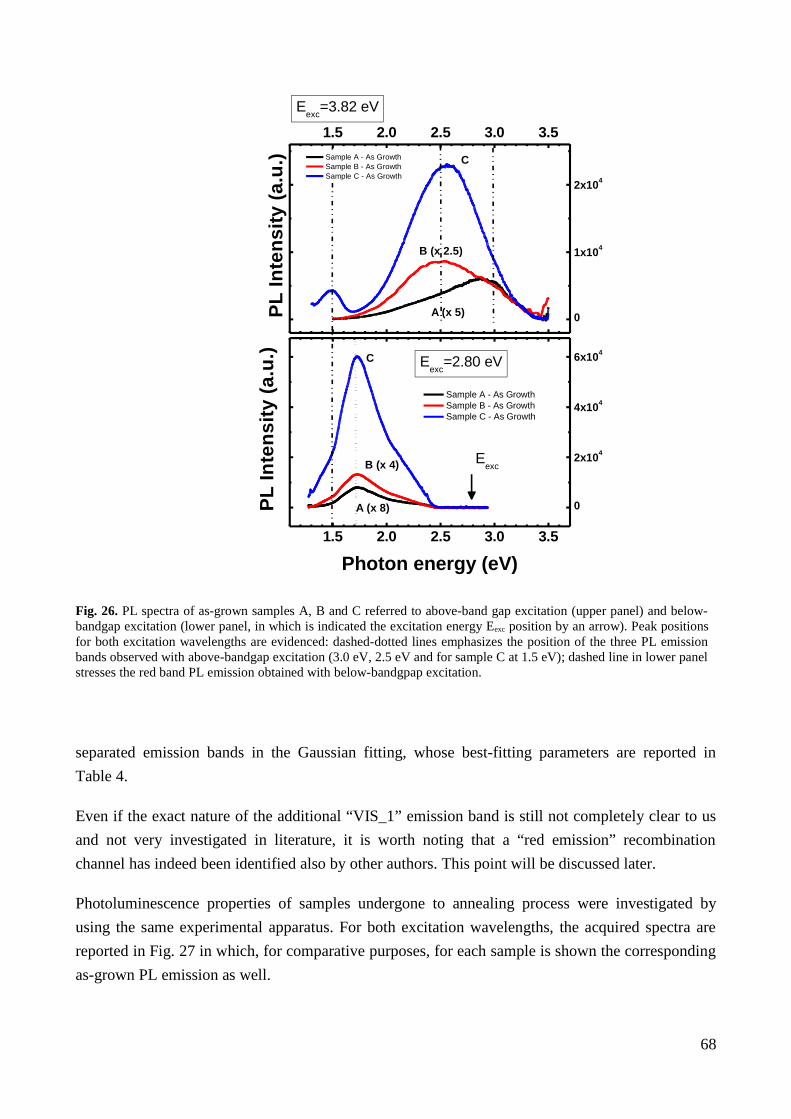
1.5 2.0 2.5 3.0 3.5
0
1x10⁴
2x10⁴
Sample A - As Growth Sample B - As Growth Sample C - As Growth
Eexc
=2.80 eV
PL
Inte
nsi
ty (
a.u
.)
Eexc
=3.82 eV
A (x 5)
B (x 2.5)
C
1.5 2.0 2.5 3.0 3.5
0
2x10⁴
4x10⁴
6x10⁴
Sample A - As Growth Sample B - As Growth Sample C - As Growth
PL
Inte
nsi
ty (
a.u
.)
Photon energy (eV)
C
B (x 4)
A (x 8)
Eexc
Fig. 26. PL spectra of as-grown samples A, B and C referred to above-band gap excitation (upper panel) and below-bandgap excitation (lower panel, in which is indicated the excitation energy Eexc position by an arrow). Peak positionsfor both excitation wavelengths are evidenced: dashed-dotted lines emphasizes the position of the three PL emissionbands observed with above-bandgap excitation (3.0 eV, 2.5 eV and for sample C at 1.5 eV); dashed line in lower panelstresses the red band PL emission obtained with below-bandgpap excitation.
separated emission bands in the Gaussian fitting, whose best-fitting parameters are reported in
Table 4.
Even if the exact nature of the additional “VIS_1” emission band is still not completely clear to us
and not very investigated in literature, it is worth noting that a “red emission” recombination
channel has indeed been identified also by other authors. This point will be discussed later.
Photoluminescence properties of samples undergone to annealing process were investigated by
using the same experimental apparatus. For both excitation wavelengths, the acquired spectra are
reported in Fig. 27 in which, for comparative purposes, for each sample is shown the corresponding
as-grown PL emission as well.
68

The above-bandgap excitation spectra of all the samples still exhibit the NBE and VIS
contributions. An overall improvement of the PL efficiency is observed when the crystal quality is
increased, suggesting that the PL efficiency is limited by disorder-related non-radiative
recombination traps. This is particularly evident for the case of sample C, where both the NIR and
the VIS activity are increased. Moreover, a correlation can be recognized between VIS contribution
and anatase content. A more accurate dissertation on these feature follow.
SampleAbove-bandgap excitation
NBE VIS NIR
AE1 =2.93 eV
σ1 =0.41 eV
w1 = 65%
E2 = 2.5 eV
σ2 = 0.7 eV
w2 =35 %
Absent
BE1 =2.93 eV
σ1 = 0.eV
w1 =12%
E2 = 2.34 eV
σ2 = 0.26 eV
w2 = 88%
Absent
CE1 = 2.89 eV
σ1 = 0.14 eV
w1 = 8%
E2 = 2.38 eV
σ2 = 0.25 eV
w2 = 86%
E3 = 1.51 eV
σ3 = 0.10 eV
w3 = 6 %Table 4. Quantities Ei , σi , wi , represent peak position, spectral width and spectral weight of the i-th Gaussianfunction, according to Eq. .
0
4x10³
7x10³
1x10⁴
1.6 2.4 3.2
Below-bandgap excitation
Annealed As-grown
Sample A
0
2x10⁴
5x10⁴
7x10⁴ Sample B
Annealed As-grown
1.6 2.4 3.2
0
3x10⁴
6x10⁴
9x10⁴Sample C Annealed
As-grown
Photon energy (eV)
0
4x10³
8x10³
1x10⁴
1.5 2.0 2.5 3.0 3.5
Annealed As-grown
Sample A
0
1x10⁴
3x10⁴
4x10⁴
Sample B
Annealed As-grown
1.5 2.0 2.5 3.0 3.5
0
1x10⁴
2x10⁴
3x10⁴
4x10⁴
5x10⁴
Sample C
Annealed As-grown
Photon energy (eV)
Above-bandgap excitation
Fig. 27. PL spectra of Titania samples obtained using λ=442 nm (left panel) and λ =325 nm (right panel) laser lines.
5.1.2 PL emission properties of as-grown vs. annealed samples: discussion69

The experimental results reported in the previous section evidence the presence of several emission
bands, corresponding to radiative transitions spanning from blue/violet to near-infrared regions of
the electromagnetic spectrum. The nature of the primary mechanisms at the origin of each of the
resonances is discussed here, based on both my experimental findings and literature support.
Generally speaking, photoluminescence activity in wide-gap semiconductors involves excitonic
states and defective states (as discussed in Chapter 2). However, excitonic properties are not
univocally defined in TiO2. In fact, since early studies on optical transitions in TiO2 carried out in
the ‘90s (Tang et al. 1995; Tang et al. 1993; Chauvet et al. 1995) it has established that the excitonic
properties of the two polymorphs (rutile and anatase) differs sensibly. A discussion on this issue is
helpful here for discussing our experimental findings.
Ionic crystals such as alkali halides or oxides are characterized by large exciton-phonon coupling
(Bosio and Czaja 1991; Liebler and Haug 1991). In this situation, the spectral properties of
excitonic states (and, in turn, the PL emission at near band-edge energies) are influenced by the
action of phonon fields on the centre-of-mass motion of (otherwise “free”) excitons. In practice,
free charge carriers interacting with ionic lattice can localize at lattice sites, building up a so-called
Sample Crystal phase Consequences of annealing on PLemissionbefore annealing After annealing
A Amorphous Rutile formation
- Both NBE and VIS still present
- No red emission
- NIR emission (1.5 eV) slightly evident
B Amorphous
Anatase formation (main effect)
Lesser content of rutile phase also evidenced
- VIS/NBE ratio increases
- Red band appearance (overcomes NIR)
- NIR emission no or slightly evident
CRutile phase already present in as-prepared samples
Anatase and Rutile formation(at comparable content)
- VIS/NBE ratio increases
- Red appearance
- NIR increases
Table 5. PL features observed before and after formation of TiO2 crystal phases by samples annealing
70

“self-trapped exciton” (STE). The theory for STE formation has been developed mainly by
Toyozawa and co-workers (Sumi and Toyozawa 1971; Schreiber and Toyozawa 1982) who
demonstrated that the self-rapping process is more likely to occur in crystals where ionic
coordination is less compact. In the particular case of anatase, the TiO6 octahedra are coordinated
only with eight neighbouring ones, while in rutile each octahedron is connected to ten neighbouring
ones. Thus, STE formation is favoured for anatase with respect to rutile.
In an important work by H. Tang and coworkers on temperature-dependent steepness of the Urbach
absorption tail in anatase (Tang et al. 1995) authors indeed demonstrated that the less coordinated
structure of anatase allows formation of STE states, while excitonic self-trapping does not occur in
rutile. In other words, excitons in anatase are self-trapped while those in rutile are free.
As the self-trapping of the charge carriers (electron and hole) is accompanied by a reduction of
excitonic energy (i.e. a finite binding energy exists), the STE emission is expected to occur at
photon energies lower than the TiO2 bandgap. For this reason, it is natural to attribute the VIS
activity and NBE activity to radiative recombination of STEs in anatase phase and rutile phase,
respectively. However, our findings suggest that the overall framework is somehow more complex,
as we discuss now.
5.1.2.1 NBE emission
We start by discussing the NBE emission, which is observed by when exciting the samples with
above-bandgap radiation. In such an excitation condition, all samples exhibit an emission band in
the blue-violet region of electromagnetic region, peaked at about 2.9 eV, both in as-prepared and
annealed conditions (see Fig. 26 and Fig. 27). We called such emission band as NBE, due to the
proximity of its energy value to the bandgap value of crystalline phases of TiO2. It is interesting to
note that such NBE contribution was not observed in below-bandgap excitation conditions: thus, it
specifically originates from interband transitions and cannot involve transitions whose initial state is
an occupied intra-gap level.
After annealing process, in no case the NBE emission was found to be dominant. Nevertheless, it
was always recognizable, i.e. well-resolved and separated from the VIS band.
Experimental findings suggest that NBE emission is anti-correlated with morphological order and
crystal phase of the TiO2 nanostructures. NBE band is, in fact, particularly evident in the case of
sample A (relative weight of about 65%), characterized by the highest degree of morphological
disorder, while its relative weight monotonically decreased in samples with more ordered
morphology and larger surface area (12% and 8% for samples B and C respectively, see
Table 4).
71

Considering also our previous discussion on excitonic properties of TiO2, it would be natural to
assign such NBE signal to free exciton recombination in rutile. In confirming this, we also note that
Sample A (where the NBE signal is the dominant one) is also the one where the relative fraction of
rutile phase on the overall crystalline phase is larger, according to XRD analysis (see section 4.2).
However, it is important to also notice that, according to XRD results, sample A was mostly
constituted of amorphous TiO2. Moreover, once the annealing conditions favoured the formation of
ordered rutile phase (see Sample C, comparing as-grown and post-annealed PL results), the most
relevant PL change was observed in the near-infrared region (NIR) and not in the NBE signal.
Therefore, we propose that the latter signal has to be attributed to the radiative recombination of the
free (i.e. not self-trapped) exciton in rutile phase and/or in amorphous TiO2. However, a different
recombination channel is dominant in rutile, which is the one in the NIR band. We anticipate that
this latter emission band is likely to be related to a specific process that occurs only at flat rutile
terraces, involving three-fold coordinated (normal) oxygen atoms on rutile (110) or (100) planes.
This can explain why the increase of the absolute (i.e. massive) amount rutile phase reflects on the
steep enhancement of the NIR (instead of NBE) signal (see sample C after annealing), while instead
the NIR signal is unobserved in the disordered sample A.
5.1.2.2: VIS emission
The VIS-PL emission manifests itself as a broad emission band peaked at about 2.4 eV and with a
full width at half maximum of approximately 550-600 meV. As mentioned previously, this
emission can be accounted different origins, including in particular radiative recombination of self-
trapped excitons in anatase and radiative recombination from surface states (Zhang, Zhang, and Yin
2000; Cavigli et al. 2009; Forss and Schubnell 1993; Lei et al. 2001; Suisalu et al. 1998). The here
reported experimental findings suggest the existence of a correlation between GBE yield, NPs
surface area and anatase crystal phase, as we discuss now.
The VIS emission in as-grown samples shows an efficiency increase passing from the more
compact structure represented by sample A (mainly compound by low-porosity assembly of
globular structures) to NPs structured sample C. This indicates a direct involving of surface states in
the mechanism leading to the GBE. The observation of an enhancement in VIS emission efficiency
is observed after annealing process. As the effect of our thermal treatment was to partially
crystallize the samples with no particular modification in the surface-to-volume ratio (Amoruso et
al. 2013), we can recognize a role of anatase surfaces (and surface states) in the VIS-PL emission.
For further discussion about this point, some consideration needs to be pointed out regarding the
surface and the oxygen vacancy states on Titania. To this aim, we can refer to the Figure 28, that
represent in the left panel an (110)-oriented Titania crystal, where titanium atoms six-fold
72

coordinated to O. The (110) plane included between points A and B consists in the same number of
Ti and O atoms, while the overall “unit” delimited by the dashed lines has no dipole moment and is
electrically neutral. Therefore, an ideal surface (i.e. neglecting reconstructions) can be obtained by
truncating the lattice as indicated in the right panel. The result is a corrugated surface, containing
two different kinds of titanium atoms. Along the [001] direction, we can find rows of normally-
coordinated Ti atoms (i.e. with coordination number 6), alternated with five-fold coordinated Ti
atoms at the surface, with one dangling bond (perpendicular to the surface). As well, two kind of
oxygen atoms exist. One is 3-fold coordinated as in the bulk (“normal” O atoms), while the other is
called “bridging oxygen” atom and miss one bond to the Ti atom (that belongs to the removed
layer). Therefore, bridging oxygen atoms is two-fold coordinated.
Surface bridging O atoms are extremely important, as their under-saturation and exposure to
external environment makes it relative easy to remove them by thermal annealing. Once removed,
the O atom leaves behind two extra electrons, filling empty states of Ti ions (and observable by
photoelectron spectroscopy (Henrich, Dresselhaus, and Zeiger 1976; Henderson et al. 2003; Nolan
et al. 2008), accompanied by a change of the oxidation state of three undercoordinated (five-fold)
titanium ions from Ti4+ to Ti3+. These latter can be think as “electron traps”, i.e. reactive sites where
an occupied electron state (or, equivalently, a “trapped electron”) is localized.
As the absorption of light creates free holes in the valence band, electron-hole transition in reduced
Titania can be therefore expected under laser pumping, as recombination of electrons trapped at Ti3+
and valence band holes. In order to find out is such transition can be invoked as origin of the VIS
band in anatase, an important suggestion comes from the computational analysis on energy position
of various defect levels in bulk anatase carried out by Di Valentin and coworkers (Di Valentin,
Pacchioni, and Selloni 2009). In this work, authors obtained that electron levels associated to Ti3+
ions coordinated with surface bridging oxygen vacancies in anatase are positioned about 2.3-2.5 eV
above the top of valence band. Moreover, experimental investigations also identifies occupied states
compatible with this energy value(Hardman et al. 1994). Such values for energy levels are in a
reasonable agreement with all of our PL results.
For the above reason, our hypothesis is that the VIS activity is mainly ascribable to the following
transition:
3 VB GBTie h hν+
− ++ →
indicating the radiative recombination between an electron trapped at (anatase) surface Ti3+ site and
a hole in the valence band. Such hypothesis matches our observation of stronger VIS signal
enhancement associated to an increase in specific surface (compare sample A with sample C) and to
an increase in anatase amount (in particular, compare the as-growth and the post-annealing PL
spectrum for samples B and C).
73
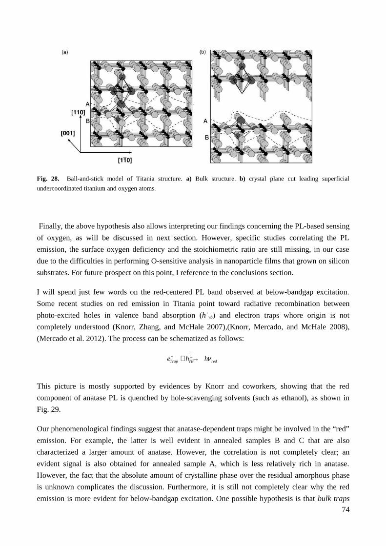
Fig. 28. Ball-and-stick model of Titania structure. a) Bulk structure. b) crystal plane cut leading superficial
undercoordinated titanium and oxygen atoms.
Finally, the above hypothesis also allows interpreting our findings concerning the PL-based sensing
of oxygen, as will be discussed in next section. However, specific studies correlating the PL
emission, the surface oxygen deficiency and the stoichiometric ratio are still missing, in our case
due to the difficulties in performing O-sensitive analysis in nanoparticle films that grown on silicon
substrates. For future prospect on this point, I reference to the conclusions section.
I will spend just few words on the red-centered PL band observed at below-bandgap excitation.
Some recent studies on red emission in Titania point toward radiative recombination between
photo-excited holes in valence band absorption (h+vb) and electron traps whore origin is not
completely understood (Knorr, Zhang, and McHale 2007),(Knorr, Mercado, and McHale 2008),
(Mercado et al. 2012). The process can be schematized as follows:
Trap VB rede h hν− ++ →
This picture is mostly supported by evidences by Knorr and coworkers, showing that the red
component of anatase PL is quenched by hole-scavenging solvents (such as ethanol), as shown in
Fig. 29.
Our phenomenological findings suggest that anatase-dependent traps might be involved in the “red”
emission. For example, the latter is well evident in annealed samples B and C that are also
characterized a larger amount of anatase. However, the correlation is not completely clear; an
evident signal is also obtained for annealed sample A, which is less relatively rich in anatase.
However, the fact that the absolute amount of crystalline phase over the residual amorphous phase
is unknown complicates the discussion. Furthermore, it is still not completely clear why the red
emission is more evident for below-bandgap excitation. One possible hypothesis is that bulk traps
74

can be involved, due to the fact that penetration depth of 442 nm radiation is larger than the 325 nm
one and that, in addition, reabsorption of back-scattered PL light leads to red-shift of the PL
spectrum. However, further studies need to be performed before to achieve a reliable interpretation.
325
Fig. 29. a) Red band photoluminescence quenching in presence of hole scavenging. such as ethanol (EtOH). b) Pictorial
representation of EtOH-induced quenching process.
5.1.2.3: NIR emission
As I stated, near-infrared emission in my experimental findings was a peculiar emission in as-grown
sample C, slightly arising in the spectra of the other two samples as well, once undergone to thermal
process. Moreover, it is interesting to notice that in sample C NIR radiative recombination
efficiency is enhanced to the detriment of the NBE one, suggesting the present of competitive
recombination pathways for a same entity involved in both emission.
Titania literature on the NIR PL is somehow limited. In fact, as we discus now, such emission band
is related to rutile Titania, while most part of recent studies deals with anatase nanoparticles due to
their enhanced photocatalytic properties. Concerning the NIR-PL, a well-established a well-
established framework of investigations has been conducted by Nakato and co-workers group at
University of Osaka (Nakamura and Nakato 2004; Nakamura, Okamura, et al. 2005b; Nakamura,
Ohashi, et al. 2005; Michael A Henderson 1999), who established that this emission band is related
to rutile Titania. Precisely, they assigned NIR PL to radiative transitions between mobile photo-
excited electrons in the conduction band and surface-trapped holes (STH) formed at triply
coordinated oxygen atoms at the surface lattice. The process of STH formation will be discussed in
75

next section, as it is quite important for the sake of explaining the oxygen-sensitive properties of PL
in our Titania nanoparticle films and of considering issues related to humidity sensing.
Our findings fully confirm the mechanism stated by the Osaka group. Firstly, we evidenced a NIR
emission in the only as-grown sample presenting a rutile signal in XRD scans. Moreover, we
alsoperformed additional analysis by PLE technique, determining the excitation spectrum of NIR
emission for annealed samples in inert ambient (i.e. under nitrogen flow).
The PLE analysis consists in extracting the intensity map of excitation vs. emission (Figure XX, left
panel). Excitation energy range from 2.1 eV to 3.3 eV was chosen for investigate both above- and
below- bandgap regions. In the right panel of Figure 30, I report the excitation spectrum of the NIR
emission, obtained through numerical integration of NIR-PL in the energy interval 1.48-1.52 eV
(delimited by the dashed line) spectral emission as function of the excitation energy.
Assuming slowly-varying quantum efficiency vs. excitation wavelength in the blue range, the PLE
signal can be considered as proportional to the optical absorbance.
The results display an onset of excitation at about 2.8-2.9 eV photon energy, i.e. at about the optical
absorption edge of rutile. In other words, no NIR-PL in rutile occurs unless above-bandgap photons
optically promote electrons to the conduction band. This evidence confirms that conduction band
electrons indeed initiate the optical transitions, as stated above.
To further support this assignment, we have also carried out PL measurements (not shown here) on
a (100)-terminated TiO2 rutile single crystal, detecting a very strong emission exactly at the same
spectral position of the NIR region. In conclusion, NIR emission has to be attributed to transitions
activated by conduction band electrons.
The occurrence of two separated PL bands in VIS and NIR region, related to different forms of
Titania, lead to interesting consequences for PL-based sensing of oxygen, as discussed in next
section.
76

2.4 2.6 2.8 3.0 3.20.0
4.0x10³
8.0x10³
1.2x10⁴
1.2 1.4 1.6 1.8
2.8
3.0
3.2
Exc
itatio
n e
nerg
y (e
V)
Emission energy (eV)
03374111148185222259296333370410
Excitation energy (eV)
PL
Inte
nsi
ty (
a.u
)
Fig. 30. Left: Excitation-resolved photoluminescence map of NIR emission (sample C). Right: excitation spectrum ofthe NIR emission integrated from 1.48 eV to 1.52 eV (delimited by vertical black dashed lines in left figure).
5.2 - Ambient gas influence on photoluminescence properties of TiO2 thin film
growth at high pressure condition
The work reported in previous chapter and in previous section indicated that Titania nanostructure
films growth with fs-PLD technique at background oxygen pressure of few mbars favours the
deposition samples with larger surface areas, while also allowing formation of rutile crystal phase.
These features result in TiO2 thin films exhibiting both a NIR emission band (fingerprint of rutile
phase) and a visible emission band, centred in the green region (tentatively attributed to electrons
trapped at surface Ti3+ sites coordinated to O vacancies at bridging positions).
The combination of these features, namely high surface-to-volume ratio, presence of both Titania
polymorphs and multiple emission bands, makes samples prepared at higher background oxygen
pressure as best candidates for exploring the influence of gas adsorption on PL properties.
Therefore, a set of samples has been prepared by fs-PLD under the same conditions used to grow
the sample C (P = 3 mbar) previously described.
The next step of my work was thus to start the investigation on PL-based response to specific gas
analytes. The choice engaged to study the effect of oxygen (O2), based on the following
considerations.
Ordinary solid-state chemical sensors based on conductometric response have to be heated in order
to speed up the adsorption-desorption kinetics and assure reversibility of the device. Moreover,
redox reactions involved in the sensing of reducing molecules (e.g. CO oxidation when reacting
77

with ionosorbed O2-) often require thermal activation energy). In our approach, PL is basically
employed as a room-temperature technique, as the sample is not intentionally heated (intentional
temperature increase usually lead also to less PL efficiency, due to activation of non-radiative
recombination channels (Bismuto et al. 2008). Therefore, a first natural candidate for investigating
PL-based detection of molecules are oxidizing gases, such as O2, O3, NO2, etc.
Nitrogen dioxide (NO2) constitutes a good choice for testing the sensitivity to oxidizing gases. NO2is an environmental pollutant (produced, for example, in internal combustion engines), so
applicative interest demands to test it diluted in ambient air environment. However, preliminary
investigation (not reported here) demonstrated that the response to air + NO2 mixtures (with NO2 at
about 20 ppm concentration, similarly to the case of ZnO studies that will be shown next) was
compatible with the response to air alone.
Successive test could confirm that the PL response had to be attributed to oxygen alone. Indeed, this
was not surprising, as Titania finds room as chemo-resistive oxygen sensor (Francioso et al. 2005;
Francioso et al. 2008; Dutta et al. 1999).
Therefore, I focused the rest of my work on PL modifications induced by O2 adsorption, which is
the subject of the present section.
5.2.1 Effect of O2 adsorption on PL emission in Titania: factual evidences
The experimental setup used for the evaluation of oxygen influence on optical properties of sample
C is described in Ch. 3, allowing detecting gas-related effects on PL emission of samples kept in
controlled atmosphere. In particular, for analyzing oxygen influence at varying concentrations, we
used controlled flows of nitrogen (N2) mixed with certified dry air. In such a configuration, inert N2
thus behave as gas carrier and O2 as analyte. The data reported here are representative for a number
of experiments performed on a series of three samples deposited by PLD at the same conditions.
Variable O2 concentration steps were performed at room temperature, while monitoring the PL,
measured with an integration time of 20 seconds and at an acquisition rate of 75 data point / hour
(approximately, one acquisition each 50 seconds). Representative experimental findings are show
in Fig. 31, where it is reported PL spectra of the sample irradiated with 325 nm laser line in two
different ambient gas condition, 100% nitrogen and 100% dry air (i.e. 20% oxygen) in stabilized
conditions (i.e. after 1 h exposure to dry air). It is evident a quenching of VIS-PL induced by
oxygen adsorption, shown in the left panel. Interestingly, NIR emission results instead enhanced
when dry air replaces N2 in the PL chamber.
For further clarity, we calculated the spectral ratio R(E) = Φ(Ε) / Φ0(E), where Φ and Φ0 represent
the PL intensity at photon energy E measured in dry air (i.e. 20% O2) and N2 atmosphere,
78

1.5 2.0 2.5 3.0 3.5
0
500
1000
1500
2000
2500
PL
inte
nsi
ty (
a.u
.)
Photon Energy (eV)
Dry N2 (100%)
Dry air (100%)
1.4 1.5 1.6
0
100
200
1.5 2.0 2.5 3.0
1
2
3
4
PL quenching
Que
nchi
ng r
atio
φ/φ
0
Photon energy (eV)
PL enhancement
Fig. 31. Oxygen influence on PL properties of TiO2 NPs thin film. Left panel: two opposite effects are generated by theadsorption of oxygen according to the PL band emission considered: GBE results quenched by oxygen, while NIRemission undergoes to an enhancement (evidenced in the inset). Right panel: Φ/ Φ0 ratio as function of emission photonenergy. NIR intensity emission in oxygen is up to 2.2 times the one in inert gas. A slighter quenching is observed forGBE.
respectively. The calculated spectral ratio is displayed in the right panel. Despite the noisiness of
the data (due to the weak experimental NIR-PL signal), the data unambiguously evidence an
enhancement of the NIR-PL emission in oxygen environment, while on the contrary the VIS-PL
intensity is quenched.
The dynamical response of VIS-PL and NIR-PL emission under flowing oxygen has been
investigated by exposing the TiO2 films to alternating steps of dry air mixed with N2 and N2 alone,
exploring O2 concentrations varying from 0.25 % to 20 %. The results are reported in Fig. 32, where
the PL intensity in the NIR and VIS band are reported as function of time. Variation of PL signal
for both emissions bands saturates vs. O2 concentration, as in a Langmuir-like trend, as
demonstrated by Fig. 33, where the measured relative response 0 0/S = Φ − Φ Φ is reported.
In conclusion, we clearly evidence that opposite effects are exerted by of oxygen on the radiative
efficiencies of the two PL bands.
It is important to stress again this point: we observed that multiple responses to the same species
(O2) is obtained by monitoring the PL intensity of mixed anatase-rutile Titania systems. This point
has to be stressed, because it represents a good example of the possible advantages of optical
approaches to chemical sensing. In fact, conductometric sensing relies on a single transduction
parameter (electrical conductance): thus, a given gas species can induce only one specific effect in
ordinary chemiresistors (i.e. electrical conductance increase of decrease). Instead, opto-chemical
routes to gas sensing can take advantage of the fact that optical properties intrinsically involve
several degrees of freedom (e.g. the continuous spectrum of PL emission wavelengths), thus
79

allowing multi-parametric responses. For those reason, I focused the rest of my studies on Titania to
propose possible interpretations of this effect, which are discussed now.
Fig. 32. Intensity of the PL emission in the visible and near-infrared range (top and bottom panel, respectively) under exposure to different concentrations of dry air.
Fig. 33. Measured absolute response for visible (black squares) and near-infrared (red circles) PL bands vs. oxygen concentration.
80

5.2.2 Effect of O2 adsorption on PL emission in Titania: supplementary investigations and
possible interpretations
As discussed in the previous section, it is natural to attribute the VIS-PL activity of anatase to
radiative recombination of electrons in gap states originated by O vacancies with photo-excited
holes in the valence band. It is worth mentioning that an analogous correlation between oxygen
deficiency and visible PL efficiency has also been evidenced in other oxides (such as SnO2 (S.
Lettieri, Causà, et al. 2008; S. Lettieri, Setaro, et al. 2008) and SiO2 (Stefano Lettieri et al. 2008).
Within this framework, a likely interpretation for the observed quenching of VIS-PL in O2 arises by
invoking the suppression of surface light-emitting Ti3+ centers. Such an interpretation can be
understood in a better way by observing the result in Fig. 34, evidencing that the occupied electron
states positioned at about 0.7 eV below the conduction band in reduced Titania (indicated as “defect
state”) vanishes after exposure to ambient oxygen. Other literature works also evidences how
gaseous O2 dissociates on titania reduce surface, filling the vacancies and destroying the defect state
(J. ‐M. Pan 1992; Kisumi et al. 2003). Attributing the VIS-PL emission to recombination of the
decay of (trapped) electron at the defect state, it is thus natural that its neutralization by ambient
oxygen leads to quenching of the VIS-PL (as observed).
Nevertheless, the observed NIR-PL enhancement under O2 flow may seem surprising at a first sight.
In fact, we previously mentioned that NIR-PL is due to radiative recombination of conduction band
electrons with STH states. According to a standard point of view, the electron-scavenging
behaviour of adsorbed O2 at rutile surface would imply a capture of mobile electrons. Once
captured, electrons would become unavailable for radiative recombination, finally leading to a
quenching of NIR-PL under O2 flow (instead of the observed enhancement).
The PLE analysis previously reported indeed indicates that free electrons are necessarily involved
in the NIR-PL. Thus, the results suggest that oxygen do not act as electron scavenger or as
ionosorbed species.
The issue is moreover complicated by our observations on O2 effect of a single-crystal
(commercial) rutile substrate that we performed as supplementary analysis. In fact, as shown in Fig.
35, we indeed observed the expected “standard” quenching of the PL by O2 when exposing a (100)
oriented and a (110) oriented rutile Titania substrate to oxygen flow (after initial exposure to
nitrogen). The introduction of oxygen leads to a fast decrease of the rutile PL of our crystals,
followed by a slow increase. The experiment was repeated several times, in all cases showing the
same trend.
In practice, two opposite effects on rutile PL are depicted in Fig. 34 and Fig. 35.
81

Fig. 34.. Photoemission spectra (hv = 35 eV, normal emission) from the valence band region of a sputtered and UHV-annealed TiO2(110) surface: room temperature adsorption of molecular oxygen results in the disappearance of thedefect state in the band gap region. (Hardman et al. 1994)
0 2000 4000 6000
0.8
1.0
1.2
PL
_N
IR in
ten
sity
(n
orm
.)
Time (s)
Rutile (100) Rutile (110)
O2 flow onN
2 flow
Fig 35. Left: dynamic response toward oxygen exposure of near-infrared PL emission of single-crystal (100) and (110)rutile substrates. Right: PL spectra measured 2 minutes after dry air exposure
82

To clarify this puzzling situation, two hypotheses have been formulated. The first one involves the
interplay between NIR-PL of residual water adsorbed at Titania surface and was tested by
performing PL analysis under prolonged UV illumination in dry vs humid air. A second
interpretation involves molecular vs. dissociative adsorption of oxygen on rutile surface and
requires analysing in detail the mechanism of STH formation.
We anticipate that a decisive proof for choosing one or another model is still missing, but the
second interpretation seems more likely at the present state.
5.3 - On “anomalous” effect of O2 on rutile Titania PL: proposed interpretations
5.3.1 First interpretation: role of residual water
The first interpretation arises from observing the behaviour of NIR-PL intensity of pure rutile
Titania reported in Fig. 35. At a first sight, the fast decrease of the PL intensity can be interpreted
according to the standard mechanism that drives the chemo-resistive effect in n-type metal oxides
(also discussed in Chapter 1), namely adsorption of molecular oxygen and capture of a conduction
band electron with formation of chemisorbed species O2-. According to this picture, the decrease in
PL intensity reflects the partial depletion of conduction band electrons during the formation of
adsorbed layer. However, it is also noticeable in figure Fig. 35 that the NIR-PL signal also
experience a slow increase, that is observed both in nitrogen and air atmosphere and was verified
for all single-crystal rutile samples, regardless the surface orientation. Moreover, the increase was
evident at continuous UV illumination, as it was in the experiment reported in figure where the laser
was impinging on the sample throughout the analysis duration.
This finding can be explained by considering the role played by the STH states in both the NIR
emission and the UV-induced photo-oxidation of water in rutile. In their first studies about this
issue, Nakano and coworkers observed that the NIR-PL activities of rutile Titania and the efficiency
of water photo-oxidation (or water splitting) process were anti-correlated. Thus, they hypothesized
that some precursor (or intermediate) of the water splitting reaction was also a state participating to
the radiative recombination of NIR-PL. Successively, they identified such a precursor in STH (self-
trapped holes) states. These latter are photo-generated holes that self-localize on surface sites at
close to oxygen bridging atoms. Using the Nakano nomenclature, the water oxidation can be
represented as the following process (Nakamura, Okamura, et al. 2005a; Kisumi et al. 2003):
[ ] [ ]2 2STHs s s
Ti O Ti H O Ti O Ti Ti O HO Ti H + + − − + → = − + − − + i
83

that indicates a nucleophilic attack of H2O at STH, with evolution of hydrogen. The trapped hole
can also recombine with conduction band electrons:
STH CB NIRe hν−+ →
and, therefore, the two processes in Eqs and are competitive in rutile.
It is thus possible to suppose that the slow increase of NIR-PL during prolonged UV illumination
shown in Fig. 35 reflects the consumption of residual water adsorbed at rutile surface, which in turn
increases the yield of the competitive reaction. This hypothesis allows to explain the behaviour
observed in bulk rutile, but it is still to be explained why the behaviour observed when both anatase
and rutile are present (as in out PLD-prepared nanoparticles) is different.
To this aim, I performed two additional experiments, monitoring the effect of dry air vs. humid air
on the NIR PL of our samples, under prolonged UV illumination (i.e. in the same conditions used
when analyzing the single-crystal rutile substrates). The excepted result is that the rise of NIR-PL
when illuminating in dry air should be larger than the one in humid air, as in the first case the
(eventual) residual H2O is consumed, while in the second it is externally supplied.
The experimental results are shown in Figs. 36 and 37.
Fig 36: Behaviour of green PL (integrated from 400 to 550 nm) and NIR PL (integrated from 700 to 850 nm) in dry airin absence (UV off) and presence (UV on) of laser illumination at 325 nm wavelength. The values are normalized to thevalue measured when UV is switched on continuously.
84

0 2000 4000 6000 8000 10000
0.6
0.8
1.0
1.2
0.6
0.8
1.0
1.2
GB_PL (400-550) NIR_PL (750-850)
UV on
Wet airUV off
Dry air
PL
Inte
nsi
ty (
a.u
.)
Time (s)
Fig. 37. Behavior of green PL (integrated from 400 to 550 nm) and NIR PL (integrated from 700 to 850 nm) in wet airin absence (UV off) and presence (UV on) of laser illumination at 325 nm wavelength. The values are normalized to thevalue measured when UV is switched on continuously.
The above results were obtained by monitoring the efficiency of both VIS-PL and NIR-PL of our
titania NPs films under O2 flow of constant concentration (dry air flow, 200 sccm) first in absence
(“UV-off”) and then in presence (“UV-on”) of continuous UV illumination. As illumination source,
we used the He-Cd laser line at 325 nm (that also provides the excitation for PL emission). In the
case of “UV-off” PL measures, the sample was illuminated only for 5 seconds (integration time for
PL spectra acquisitions) and was kept in the dark for the rest of the time. In the case of “UV-on”
measures, the sample was kept under laser illuminated for the entire duration of the experiment. In
both cases, before the experiment the sample was kept for several hours (14 h) under dry air flow in
order to stabilize it and rule out PL modification ruled by variation in the gaseous environment
inside the test chamber. Measurements in wet air were obtained by flowing air in a bubbler
containing bi-distilled water.
As expectable, no significant modification of the PL efficiencies was observed in the case of
occasional and short illumination (“UV-off”), while again an opposite trend for NIR-PL and VIS-
PL efficiency was observed in all cases under effect of UV light, thus confirming the previously
shown results.
The quenching of visible emission is found in both experiments, while the finding to be noted is that
the enhancing effect of oxygen on NIR emission is attenuated in presence of humidity, even if still
85

present. In particular, an enhancement slightly larger than 40% is obtained in dry air, while the
presence of H2O reduces it to less than 20%. This is indeed the expected result, if assuming that the
eventual residual water is replaced by other water molecules supplied by the external flow.
To point to be explained is now why this finding is not observed in pure rutile samples. Regarding
this point, we speculate that a possible cause may involve the oxygen-assisted diffusion of adsorbed
water molecules, described by Wendt and coworkers (Wendt et al. 2006).
In fact, from the relative weight of PL spectra shown in Fig. 31, it is reasonable to guess that the
overall rutile amount is much less than the anatase one. Moreover, photocatalytic activity of anatase
Titania is usually more efficient than the rutile Titania one (Diebold 2003). Thus, water molecules
are expected to have a shorter mean free path in anatase, before being consumed by UV-activated
photosplitting in oxygen environment. A pictorial representation of the proposed mechanism is
shown in Fig. 38.
The concomitant occurrence of larger amount of anatase and of shorted diffusion length in anatase
lead to the fact that water adsorbed at rutile crystallites dispersed in a more abundant anatase matrix
is consumed more efficiently than respect to the case of bulk rutile. This can result in the fact that
the (slow) enhancement effect in mixed PLD-prepared samples is the dominant one, while it is a
minor effect in bulk rutile.
Fig. 38. Pictorial representation of water migration in Titania
86

To reinforce this point, it is worth noting that the quenching effect of O2 on NIR-PL observed in
bulk rutile is quite fast and much faster than the enhancing effect shown in Figs. 36 and 37, while
the characteristic time of this latter is comparable to the enhancing effect.
Even if the mechanism proposed here fits with the experimental findings and with literature results,
some major issues remain. For example, it relies on several ad-hoc hypothesis, in particular: 1) the
actual presence of residual water adsorbed at nanoparticle surfaces, and: 2) the validity of the
interpretations given in Ref. (Wendt et al. 2006). Moreover, it is suspicious that two apparently
uncorrelated effects such as neutralization of Ti3+ states (attributed to oxygen adsorption) and inter-
phase diffusion of water lead to two effects (decrease of VIS-PL and increase of NIR-PL) that
exhibiting similar characteristic times, as one can see in Figs. 36 and 37.
Therefore, I propose also a second interpretation, assuming that dissociative adsorption is the
preferred route for oxygen adsorption in reduced rutile.
5.3.2 Second interpretation: dissociative adsorption
Here we remark that a different interpretation can be given to explain the apparently opposite
effects of oxygen on rutile PL. The interpretation assumes that adsorption of oxygen on rutile
surface can proceed along two possible different routes: one as “standard” ionosorption (leading to
PL quenching), and another as dissociative adsorption, where oxygen does not capture a conduction
band electron, but instead simply dissociates and fills the oxygen vacancy. This second process is
expected to enhance the rutile PL. To show why, we need to review the process of STH formation.
Surface trapped holes involved in water photo-splitting consists in consists in the trapping of photo-
generated holes on surface sites of 3-fold coordinated (normal) oxygen atoms. Following Nakano
and co-workers, STH formation can be represented as follows:
[ ] [ ]2 2VBs sTi O Ti h Ti O Ti
++= − + → = iii
where h+VB is a valence band hole that self-traps on the surface O-sites residing in (100) and (110)
rutile surfaces.
It is important to underline that the process is localized at three-fold surface oxygen atoms: thus,
the oxidation of rutile surfaces is expected to favour the STH formation and, in turn, to increase the
NIR-PL efficiency. We notice that this behaviour is opposite to the anatase one, where surface
oxidation is expected to decrease the VIS-PL efficiency instead.
Therefore, we hypothesize that the results we observed for NIR-PL efficiency can be explained by
invoking the fact that molecular oxygen dissociation and surface oxidation under UV illumination is87

the dominant process when O2 interacts with more defective (oxygen deficient) rutile surfaces,
while instead the formation of ionosorbed species O2- (inducing PL quenching) can take place on
less defective surfaces.
Even if we do not have a direct proof for the validity of this interpretation, it relies on less ad-hoc
hypothesis than the previous one. Moreover, it invokes the same process at the basis of VIS
quenching and NIR enhancing, thus explaining naturally why the time behavior of is similar.
Indeed, performing an exponential fit of the data in Figure 36 (dashed lines) as follows:
( )( )
( ) (0) 1 exp
( ) (0) exp
NIR NIR NIR
VIS VIS NIR
t t
t t
τ
τ
Φ = Φ ⋅ − −
Φ = Φ ⋅ −
compatible (within error bars) values of ( ) 3 1.9 0.2 10 NIR sτ = ± ⋅ and
( ) 3 2.0 0.1 10 VIS sτ = ± ⋅ have been obtained. This further reinforces the interpretation.
Finally, we wish to point out that our experimental results are quite close to the ones recently
reported by Knorr and coworkers (Knorr, Mercado, and McHale 2008). These authors showed that
when exposing anatase-rutile mixed systems of anatase and rutile to air and H2O2, a different NIR-
PL behavior is observed with respect to the one observed in pure rutile. In particular, a quenching of
anatase VIS-PL and an increase of the rutile NIR-PL intensity occurred in the case of mixed
systems, while on the contrary a only a moderate quenching of the NIR-PL intensity was observed
in pure rutile samples.
Authors interpreted these results by suggesting that the presence of oxidizing species may trigger an
interphasial electron transfer, i.e. transfer of conduction band electrons from anatase to rutile. Our
interpretation is different and, in particular, we find it quite difficult to explain why electrons
scavenged from anatase by oxygen should be next transferred to rutile. However, the
phenomenological evidences we show here are in agreement with the observations by Knorr and
coworkers. This fact strengthens the reliability of our experiments.
5.4 – An investigation on PL-based sensing of nitrogen dioxide by ZnO thin films
Another material studied in my PhD work was zinc oxide (ZnO). As discussed in the introduction,
ZnO exhibits a stable and efficient photoluminescence emission in the UV range even at room
temperature, making it a material of interest as light emitter.
My studies on ZnO were conducted in the framework of collaboration with University of Ferrara,
where nanostructures and microstructures exhibiting different topologies have been prepared by sol-
gel method.
88

Previous investigations demonstrated that reversible PL modification in ZnO occur once the
samples are exposed to nitrogen dioxide (NO2) (Baratto et al. 2009; Cretì et al. 2012; Padilla-Rueda,
Vadillo, and Laserna 2012a; Valerini, Cretì, A.P. Caricato, et al. 2010). In particular, NO2 sensing
properties exploited by PL modulation have been investigated in ZnO nanowires (Baratto et al.
2009; Cretì et al. 2012), thin films (Padilla-Rueda, Vadillo, and Laserna 2012a) and nanostructured
surfaces (Valerini, Cretì, A.P. Caricato, et al. 2010) proving that ZnO exhibits an efficient and fast
quenching of UV PL at room temperature when NO2 surround the oxide.
Unfortunately, the above mentioned works relied on static PL measurements only. As discussed in
Chapter 2 (see the discussion about the static vs. dynamic quenching mechanisms), this fact limited
the conclusions that can be expunged about the basic mechanisms driving the sensing phenomenon.
In particular, we recall the importance of time-resolved photoluminescence analysis (which in this
particular case translates in exciton lifetime measurements) in samples subject to the same external
conditions that give rise to the PL modulation (for a discussion on this issue we refer to Ref. (S.
Lettieri, Setaro, et al. 2008). In the course of my work, I focused on the role played by sample
topology in the ultraviolet (UV) PL quenching induced by the interaction with NO2. To this aim, we
carried out experiments based on both static and time-resolved photoluminescence (TRPL) on ZnO
samples exhibiting different topologic characteristics. Comparing and correlating the results
obtained for the different samples under exposure to air and to NO2, basic consideration about the
origin of ultraviolet photoluminescence quenching could be outlined.
In Fig. 39 it is depicted the schematic procedure used to synthesize ZnO nanoparticles, while
different structures could be obtained by addition of proper surfactants at in the sol and/or
modifying the calcination temperatures (M. Carotta, unpublished results). Up to four type of
structures have been prepared by University of Ferrara and analysed during my work, but only two
of them are reported here, as they exhibit somehow “opposite” topologies.
SEM images of the structures investigated are reported in Figs.40 and 41, and are named as ZNP
(i.e. ZnO nanoparticles) and ZFL (i.e. ZnO “flowers”). While ZNP consists of a porous assembly of
nanoparticles with typical sizes of about 60 nm, in ZFL samples we observe the formation of
hexagonal rods assembled in flower-like structures. By the SEM images it is evident that ZFL is
composed by interconnected structures that support electronic transport, while instead in ZNP
sample charge motion occurs trough grain boundaries (as in most of chemoresistive
semiconductors).
Therefore, we might say that ZNP can be used as a “standard” sample for chemical sensing analysis
89

Fig. 39. Schematic procedure for sol-gel synthesis of ZnO nanostructures
while we chose to characterize ZFL due to its diversity with respect to nanoparticle ensembles.
The photoluminescence analysis was conducted by using the same apparatus previously described
and employed for Titania studies. The analyzed samples exhibited the typical ZnO PL spectrum,
with a near band edge emission at 380 nm (UV) due to radiative excitonic recombination, and a
broad band visible, peaked at 675 nm (orange), usually adduced to zinc vacancy or interstitial
oxygen atoms (Studenikin, Golego, and Cocivera 1998b; Djurišić et al. 2007b). An example of PL
spectrum is shown in Fig. 42, where the excitonic emission is evidenced by the colored rectangle. In
my work only this latter emission was investigated, as the presence of the various kind of defects
leading to the visible emission is neither necessarily nor clearly correlated with the sample
topology.
Measurements of UV emission in NO2 diluted in dry air were performed, exposing samples for 15
minutes to 10, 30, 50 and 90 ppm of NO2 in air, alternating NO2 exposures with dry air steps. The
dynamic response is reported in Fig. 43, where is shown the PL intensity integrated in the range 370
nm to 410 nm) as function of time.
The PL variation induced by gas exposure is quantified by the integrated PL as the total intensity of
the spectrum (or spectral emission) over the emission interval:
90

Fig. 40. ZNP sample, consisting in an homogeneous ensemble of ZnO nanoparticles of about 60 nm averagediameter
Fig. 41. ZFL sample, consisting in agglomerated flower-like structures composed of micrometer-scale single-crystalZnO (please notice the exagonal facets of each microstructure)
91

2
1
( ) ( , )t t dλ
λ
ϕ λ λΦ = ∫
where ( , )tϕ λ is the PL spectrum acquired at time t.
As expected from previous works (Comini et al. 2007; Baratto et al. 2009; Cretì et al. 2012; Padilla-
Rueda, Vadillo, and Laserna 2012b; Valerini, Cretì, A. P. Caricato, et al. 2010; Caricato et al. 2011)
UV emission is quenched by the presence of NO2 gas molecules. Although the PL signal recovery
in air is almost complete, a partial irreversibility is evident after some cycle.
In Fig. 43 the relative response ( )2air air NO air∆Φ Φ = Φ − Φ Φ is reported, evidencing a Langmuir-
like behaviour and quantifying the fact that ZNP sample has the most efficient response.
As discussed in Chapter 2, a quenching of PL signal can derive by different mechanism, involving a
change in the decay rates (dynamic quenching) of a decrease in the density of emitting centres
(static quenching). A clear discrimination between these two situations is impossible with the only
CWPL, while time-resolved PL technique allows a direct measure of recombination lifetime (whose
eventual changes are the signature of dynamic mechanisms).
Therefore, TRPL measurements were also performed, while keeping the samples in dry air and in
100 ppm NO2 (diluted in dry air).
300 400 500 600 700 800 900
1
10
PL
inte
nsi
ty (
a.u
)
Wavelength (nm)
ZNP
Fig. 42. Typical PL spectrum of ZnO (ZNP sample). The shadowed area evidences the excitonic emission, which hasbeen the subject of the present dissertation.
92

Fig. 43. a) UV-PL intensity vs. time under exposure to 10, 30, 50, 70 and 90 ppm of NO2 in air. b) UV-PL response
versus NO2 concentration
The results are shown in Fig. 44. It is easy to see that no modification of the exciton lifetime occur
when NO2 is introduced, indicating the occurrence of a static mechanism. Moreover, the exciton
lifetime in ZFL is about 4 times longer than the one in ZNP. Such a difference was repeatedly
observed by performing several TRPL measurements on different point of each sample and on
different samples of the same typology. Thus, the different exciton lifetime cannot be simply
attributed to sample-to-sample variability. Indeed, this difference plus the observation of lifetime
constancy when samples are exposed to the PL quencher allows to sketch an interpretation of the
PL quenching phenomenon, based on the inhibition of exciton formation (or “excitonic depletion”,
93

as we name it in the following subsection). The efficiency of such mechanism is expected to depend
relevantly on the sample topology, as we discuss now.
5.4.1 Interpretation: excitonic depletion and role of the topology
It is well known that all excitons in ZnO are bound at cryogenic temperatures, i.e. are localized to
point defect sites (such as group-IV dopants). As the temperature is raised, the thermal energy
becomes larger than the binding energy of exciton-defect complex and become mobile. At room
temperature, the ZnO excitons are all free and, therefore, their recombination lifetime also becomes
dependent of its motion. As a matter of fact, moving excitons typically dissociate when bump at an
interface or at a boundary of a semiconductor grain. Therefore, while in structures whose typical
size far exceeds the exciton mean free path the lifetime is not size-dependent, the situation is
different for confined structures. In this latter case, the volume available for exciton motion shrinks
and a surface recombination lifetime has to be introduced, limiting the total recombination lifetime.
The correlation between exciton lifetimes and nanostructure sizes and topology have been reported
in literature (Kwok et al. 2005; Xiong, Pal, and Serrano 2007), evidencing that the decay times of
ZnO nanorods increase as the size increases (Hong et al. 2003). On this basis, it is natural to ascribe
the longer ZFL exciton lifetime to the fact that the topology of such structures favours the free
motion of excitons, without limitations due to inter-grain boundaries. Indeed, the “base units” of
ZFL samples are micro-rods whose size is in the micrometer scale. Moreover, such rods are
internally connected. On the contrary, exciton motion in ZNP is limited by grain boundaries.
0 100 200 300 400 500
1E-3
0.01
0.1
1
TR
PL
sig
nal
(a.
u.)
Time (ps)
ZFL in air ZFL in NO
2
ZNP in Air ZNP in NO
2
Fig. 44. Peak-normalized time-resolved decay of UV-PL for ZFL (blue curve) and ZNP (red curve)samples measured in air (full curves) and in 100 ppm NO2 (dashed lines).
94

Fig. 45. Representation of the NO2 induced enlargement of depletion region at grain boundary. Apartcorrections dependent on the grain diameter, the Shottky barrier (i.e. energy barrier separating the coreundepleted region and the grain boundary) scales as L2, where L is the width of depleted region.
Considering also the NO2-independent lifetimes measured by TRPL, a natural interpretation for the
PL quenching arises, starting from the assumption that “standard” chemoresistive modulation of
Schottky barrier and of space charge depletion occurs when NO2 is adsorbed at surfaces. We show
schematically this in Fig. 45, where the charge-depleted sub-surface (white) region is represented.
Assuming that adsorption of NO2 enhances the Schottky barrier (or, equivalently, enlarges the
depleted region), we obtain the situation represented in Fig. 46 where, electrons and holes formed
by photon absorption within the sub-surface region. As the exciton formation is not instantaneous
but typically requires about 50-80 ps in bulk ZnO (results obtained on single-crystal ZnO, not
reported here for brevity reasons), the built-in electric field can lead to separation of electrons and
holes even before the exciton formation. The residual e-h pair, possibly formed far from the
Schottky barrier, can then undergo to formation of free excitons moving in the ZnO structure with a
lifetime depending on the sample topology (as previously discussed) but not on the presence of
adsorbed NO2.
95

96

Conclusions
Over the course of my Ph.D. career, I devoted my work on the analysis of phenomena linking the
photoluminescence activity of some specific metal oxides to oxidant chemical species. The
materials I have been involved in were titanium and zinc oxides (TiO2 and ZnO), prepared as
nanostructured thin films and whose optical properties were investigated by means of
photoluminescence spectroscopy. My activities involved various phases of the project, including:
sample deposition, structural and basic optical characterization, set-up of the experimental system
allowing PL-based opto-chemical analysis and, finally, experiments on oxygen and nitrogen
dioxide-related effects on the photoluminescence properties of the investigated materials.
Photoluminescence spectroscopy is an important tool often used for the characterization of
semiconducting metal oxides, based on wavelength-resolved (and, possibly, time-resolved)
detection of radiative recombination processes between charge carriers in a material. Analysis of PL
spectrum allows the reconstruction of energy distribution levels in a material, strictly correlated
with its structural and morphological characteristics: crystallinity, defects states, surface states, free
or trapped excitons and free charge carriers, are just some examples of possible elements
influencing and characterizing the PL emission of a material. The knowledge on energy level
distribution, physical nature and participant of processes at the base of PL emission is of course
particularly useful in view of studies of metal oxide applications.
A relatively unexplored approach in the field of metal oxide-based gas sensing approaches is
represented by the opto-chemical sensing based on PL modulations. In such an approach, PL
emission of a material is used to probe the presence of ambient gas molecules: variation in
environmental atmosphere components and adsorption processes may lead, in fact, to a modulation
of PL emission of a material. Several factors influence adsorption of gas molecules on a material,
including the mutual reactivity between gas and material components, the existence of available
adsorption states, external pressure (or equivalently, analyte concentration) and temperature.
Moreover, sample topology, surface-to-volume ratio and overall defect concentrations (e.g. oxygen
deficiency) all play a fundamental role.
In the course of my work, TiO2 and ZnO were grown with different deposition conditions, leading
to structures with different morphology. SEM and XRD tools allowed having a clear picture on the
morphological and structural properties of the samples and a crossed analysis with room
temperature PL spectra lead to a satisfactory knowledge on the physical origins of the different
mechanisms at the base of PL properties of the samples. After a preliminary structural and optical
characterization, an investigation on the property in gas sensing for both material has been
performed.
97

A particular attention has been devoted on the TiO2 nanostructures for several reason. In particular,
PL properties of TiO2 are less well-characterized with respect to the ZnO ones (ZnO is very
important as UV light-emitting material) and its PL emission is far less efficient than the ZnO one
(TiO2 is an indirect gap material, while ZnO has direct gap). Furthermore, a clear consensus on the
chemical nature of various defects involved in the sub-bandgap PL emission of TiO2 has not been
established already. Different states emitting in the same range of wavelength (such as self-trapped
exciton in anatase and oxygen vacancies-related states), the possibility of having different stable
crystal phases, surface and reactive state defects, represents some of the variable influencing PL
emission and a careful analysis should be necessarily put for having a good interpretation of the
optical properties of TiO2.
TiO2 nanostructured thin films deposition was performed with the ultrafast pulsed laser ablation,
using laser pulses in femtosecond regime, a relatively recent and appealing deposition technique
still less exploited for TiO2. Great interest, thus, grew up around the analysis of physical properties
of the so growth TiO2 samples. Three different oxygen pressure regime were using for the
deposition (10-6 mbar, 1 mbar and 3 mbar) leading to nanostructures with different morphologies:
for high vacuum, a low-porosity NPs agglomerated assembly to high specific surface samples, with
more isolated NPs (size from 20 nm to 100 nm) for the highest pressure condition.
As-grown samples showed a degree of crystallinity, increased after an annealing process (500°C for
30 min in ambient air). The specific structural and morphological features (crystal phase and high
surface-to-volume ratio), made me have propensity for the sample growth in high pressure
condition for further analysis on gas probing. PL emission modulation in alternate gas condition
was monitored.
In the successive stage of my work, I mainly concentrated on oxygen effect on TiO2 PL properties.
The attention was focused on two bands emission, in the visible region and in the near-infrared
region (respectively VIS-PL and NIR-PL). The two separated bands are found to be fingerprints of
the two TiO2 polymorphs, namely anatase (VIS-PL) and rutile (NIR-PL).
Very interestingly, the behaviour of such emission bands in oxygen ambient gas resulted to be
anticorrelated: a quenching in VIS band corresponded, in fact, to an enhancing in the NIR band
upon exposure to oxygen.
Such a result triggered considerable attention, as indicating that multiple responses to the same
species (O2) can indeed be obtained by monitoring the PL intensity of mixed anatase-rutile titania
systems. This fact deserved further investigation, as being a good example of the possible
advantages of optical approaches to chemical sensing. In fact, conductometric sensing relies on a
single transduction parameter (electrical conductance): thus, a given gas species can induce only
one specific effect in ordinary chemiresistors (i.e. electrical conductance increase of decrease).
Instead, opto-chemical routes to gas sensing can take advantage of the fact that optical properties
98

intrinsically involve several degrees of freedom (e.g. the continuous spectrum of PL emission
wavelengths), thus allowing multi-parametric responses. Moreover, it is worth underlining that the
trend for the NIR emission was somehow unexpected at first sight, considering the well-known
activity of molecular oxygen as electron scavenger (manifested indeed in our experiments on rutile
single crystals).
This peculiar effect of oxygen on rutile PL was subjected to additional study, and two
interpretations are given here, one based on the nature of adsorption process of oxygen
(ionosorption vs dissociative adsorption) and another on diffusion of residual water molecules
adsorbed at TiO2 nanoparticle surfaces.
In the discussion reported in Chapter 5 I finally argue why I am more inclined to the first
interpretation. According to this latter, TiO2 nanostructured thin film should present an high
concentration of oxygen vacancies. In such a condition, ambient oxygen undergoes to a preferential
dissociative adsorption, supplying an O atom at surface bridging positions that saturates the oxygen
vacancies. This, in turn, lead to both the decrease of VIS-PL and to the increase of NIR-PL, as
explained along Chapter 5. On the contrary, in the case of well-oxidated surfaces and/or in the case
of non-porous morphologies (i.e. low surface-to-volume ratios) such process is negligible, and the
dominant oxygen effect can become the ionosorption (i.e. chemorption of oxygen in ionic state O2-
with scavenging of electrons from conduction bands and quenching of rutile PL).
Even though further analysis should be performed for having propensity for one interpretation with
respect to the other, it is clear the high efficiency oxygen sensing properties of TiO2 nanostructures:
the anticorrelated trend of the two emissions, in fact, can be consider as a fingerprint of oxygen gas
molecules adsorption since the modulation of the two emission is strictly oxygen-dependent.
Moreover, the opposite effect produced by one specie-analyte (oxygen) on two different PL band, is
helpful for an easy detection of gas mixture, representing a great advantage with respect to the
common conductometric gas sensors. However, worth mentioning is the double-edge sword
represented by photocatalytic properties of TiO2: in this material, photocatalytic effects are likely to
occur, thus leading to lacking repeatability and stability of the system. Further investigations are
definitely to be made in this topic.
ZnO material has instead been demonstrated to be highly efficient in detecting NO2, with a larger
response for nanoparticle thin films with respect to flower-like structure, by means of CWPL and
TRPL spectroscopy. The analysis of PL decay time in air and NO2 atmosphere is an evidence of the
static quencher nature of gas molecules. Differences in exciton lifetimes for the two structures
investigated (smaller in nanoparticle thin film) are observed, reflecting in “topological” properties
and on the excitonic mean free path. Energy barrier modulation induced by adsorption of NO2
(likely to be ionosorption as NO2- species) affects the formation of excitons, thus explain the
observed results and giving a coherent frame for the static quenching mechanism observed.
99

Acknowledgements
With the end of this work, another chapter of my life is finished as well and, as for good tradition, it
is not possible ending something without stopping a bit for reviewing on the past time.
Looking back at these three years, as a Ph.D. student, I cannot not consider myself very lucky for
the possibility I had to work with my supervisors prof. Pasqualino Maddalena and dott. Stefano
Lettieri. Three years ago, they introduced me, a regretful “theoretician”, to a field completely new
for me and by sharing their knowledge with constant and patient support, they allowed me to “grow
up” and being more and more familiar with what concern the world of spectroscopy. And a
particular, sincere gratitude is for Stefano, that, more than a supervisors, I can consider as my
mentor. Hope for them I was at overall an equivalently good student. I would like to thank my
internal referees as well, prof. Antonio Cassinese and prof. Domenico Ninno for their suggestion
during the going on of my work.
Sincere gratitude is for prof. Salvatore Amoruso and the “Laser ablation” group, too: without his
kind helpfulness during the work in his laboratory, part of the “raw matter” on which my work was
build on could not existing! Same thanks is going to prof. Nikolay Nedialkov and prof. Peter
Atanasov, from the “Institute of Electronics”, Bulgarian Academy of Sciences
in Sofia (Bulgaria) for kindly hosting me in their institute and in their beautiful city during the
bilateral project with prof. Amoruso’s group.
A special thank is for our “polar star” Guido Celentano: with his kindness, his rigor in its job and
his punctual reminders on deadlines, he represents a referring point for all the Ph.D. students
passing throug the Physics Department (and not only, I guess!)
As a student, a place in this acknowledgements is surely deserved to my friends, with whom I
shared unforgettable days. Worth nothing my international friends, that allowed me to
be in contact with cultures I could never image I was going to interact and teach me how much
small in reality is the world, with distances sometimes existing only from the geographic point of
view. With them I loved persian food and enjoyed with farsi language, I learnt how to swear in
russian and speak a bit of kurdish, I increased my background of jokes... (I wonder if Abol or Sergei
have some jokes about Ph.D. students!). Behzad with his constant support and friendship in these
last months, Ehsan and Mohadeseh, my first teachers of persian Abolfazl and Arash fo the iranian
side, the never ending Sergei, Fatema, Aldencik, Oktay and Asuman and their love for Turkey...
and, even to don't forget my italian origin, how can I don't mention Mariano, Alan, Lorenzo, my
“labmate” Emanuele and all my old friends who accompanied me during my university years in
Naples?
100

Even if sooner or later our ways will be separated, for each of you, I will always preserve at least
one memory in my mind. My wonderful life in university would not have been the same without
you.
And finally, last, but not least, I must thank my family and in particular my mother, to whom I will
be eternally grateful for her infinite support in all my choices during all my life.
101

Bibliography
Alivov, Ya I., J. E. Van Nostrand, D. C. Look, M. V. Chukichev, and B. M. Ataev 2003 Observationof 430 Nm Electroluminescence from ZnO/GaN Heterojunction Light-Emitting Diodes. AppliedPhysics Letters 83(14): 2943–2945.
Alivov, Ya. I., D. C. Look, B. M. Ataev, et al. 2004Fabrication of ZnO-Based Metal–insulator–semiconductor Diodes by Ion Implantation. Solid-State Electronics 48(12): 2343–2346.
Amoruso, S. 1999 Modeling of UV Pulsed-Laser Ablation of Metallic Targets. Applied Physics A69(3): 323–332.
Amoruso, S., C. Aruta, R. Bruzzese, X. Wang, and U. Scotti di Uccio 2011 Substrate HeatingInfluence on the Deposition Rate of Oxides during Pulsed Laser Deposition in Ambient Gas.Applied Physics Letters 98(10): 101501.
Amoruso, S., G. Ausanio, R. Bruzzese, M. Vitiello, and X. Wang 2005 Femtosecond Laser PulseIrradiation of Solid Targets as a General Route to Nanoparticle Formation in a Vacuum. PhysicalReview B 71(3): 033406.
Amoruso, S., R. Bruzzese, N. Spinelli, R. Velotta, M. Vitiello, X. Wang, et al. 2004 Generationof Silicon Nanoparticles via Femtosecond Laser Ablation in Vacuum. Applied Physics Letters84(22): 4502 –4504.
2004 Emission of Nanoparticles during Ultrashort Laser Irradiation of Silicon Targets.Europhysics Letters 67(3): 404–410.
Amoruso, S., R. Bruzzese, X. Wang, and J. Xia 2008 Ultrafast Laser Ablation of Metals with a Pairof Collinear Laser Pulses. Applied Physics Letters 93(19): 191504.
Amoruso, S., B. Toftmann, and J. Schou 2004 Thermalization of a UV Laser Ablation Plume in aBackground Gas: From a Directed to a Diffusionlike Flow. Physical Review E 69(5): 056403.
Amoruso, S., S. Tuzi, D. K. Pallotti, et al. 2013 Structural Characterization of Nanoparticles-Assembled Titanium Dioxide Films Produced by Ultrafast Laser Ablation and Deposition inBackground Oxygen. Applied Surface Science 270: 307–311.
Amoruso, Salvatore, M. Vitiello, and X. Wang 2005 Femtosecond Laser Ablation and Deposition,Pulsed Laser Deposition of Optoelectronic Cap2 - Optoelectronic Materials and Devices Volume 2:Pulsed Laser Deposition of Optoelectronic Films Da Mihai A. Popescu (editor): INOE Hardcover -A Squared Books (Don Dewhirst). http://www.abebooks.it/Optoelectronic-Materials-Devices-Volume-Pulsed-Laser/9270443002/bd, accessed March 29, 2014.
Andreić, Ž, L Aschke, and H. -J Kunze 2000 The Presence of Droplets in Pulsed Laser Deposition
102

of Aluminum with Capillary Ablation Targets. Applied Surface Science 153(4): 235–239.
Anisimov, S. I., B. S. Luk’yanchuk, and A. Luches 1996 An Analytical Model for Three-Dimensional Laser Plume Expansion into Vacuum in Hydrodynamic Regime. Applied SurfaceScience 96–98. Proceedings of Symposium F: Third International Symposium on Laser Ablation ofthe 1995 E-MRS Spring Conference: 24–32.
Aranovich, Julio A., Dolores Golmayo, Alan L. Fahrenbruch, and Richard H. Bube 2008Photovoltaic Properties of ZnO/CdTe Heterojunctions Prepared by Spray Pyrolysis. Journal ofApplied Physics 51(8): 4260–4268.
Aruta, C., S. Amoruso, R. Bruzzese, et al. 2010 Pulsed Laser Deposition of SrTiO3/LaGaO3 andSrTiO3/LaAlO3: Plasma Plume Effects. Applied Physics Letters 97(25): 252105.
Ashfold, Michael N. R., Frederik Claeyssens, Gareth M. Fuge, and Simon J. Henley 2004 PulsedLaser Ablation and Deposition of Thin Films. Chemical Society Reviews 33(1): 23–31.
Ashrafi, A. B. M. Almamun, Akio Ueta, Adrian Avramescu, et al. 2000 Growth andCharacterization of Hypothetical Zinc-Blende ZnO Films on GaAs(001) Substrates with ZnS BufferLayers. Applied Physics Letters 76(5): 550–552.
Atkins, P. W 2010 Shriver & Atkins’ Inorganic Chemistry. Oxford; New York: Oxford UniversityPress.
Ausanio, G., A. C. Barone, V. Iannotti, et al. 2004 Magnetic and Morphological Characteristics ofNickel Nanoparticles Films Produced by Femtosecond Laser Ablation. Applied Physics Letters85(18): 4103–4105.
Ausanio, G., V. Iannotti, S. Amoruso, et al. 2012 Effects of Substrate Temperature on Nanoparticle-Assembled Fe Films Produced by Ultrafast Pulsed Laser Deposition. Applied Surface Science258(23): 9337–9341.
Baratto, C., S. Todros, G. Faglia, et al. 2009 Luminescence Response of ZnO Nanowires to GasAdsorption. Sensors and Actuators B: Chemical 140(2): 461–466.
Barsan, N. 1994 Conduction Models in Gas-Sensing Sno2 Layers - Grain-Size Effects and AmbientAtmosphere Influence. Sensors and Actuators B-Chemical 17(3): 241–246.
Bates, Carl H., William B. White, and Rustum Roy 1962 New High-Pressure Polymorph of ZincOxide. Science 137(3534): 993–993.
Baur, W. H. 1961 Atomabstände Und Bindungswinkel Im Brookit, TiO2. Acta Crystallographica14(3): 214–216.
Becke, A. D. 1988 Density-Functional Exchange-Energy Approximation with Correct Asymptotic
103

Behavior. Physical Review A 38(6): 3098–3100.
Bieber, Herrade, Pierre Gilliot, Mathieu Gallart, et al. 2007 Temperature DependentPhotoluminescence of Photocatalytically Active Titania Nanopowders. Catalysis Today 122(1–2):101–108.
Bismuto, A., A. Setaro, P. Maddalena, L. De Stefano, and M. De Stefano 2008 Marine Diatoms asOptical Chemical Sensors: A Time-Resolved Study. Sensors and Actuators B: Chemical 130(1):396–399.
Blanchet, Graciela B., and Curtis R. Fincher 1994 Thin-Film Fabrication by Laser Ablation ofAddition Polymers. Advanced Materials 6(11): 881–887.
Boer, Jan Hendrik 1953 The Dynamical Character of Adsorption. Clarendon Press.
Bosio, C., and W. Czaja 1991 Urbach Tails in the Absorption Spectra of Amorphous andCrystalline SiO2. Philosophical Magazine Part B 63(1): 7–14.
Bulgakova, N. M., R. Stoian, A. Rosenfeld, I. V. Hertel, and E. E. B. Campbell 2004 ElectronicTransport and Consequences for Material Removal in Ultrafast Pulsed Laser Ablation of Materials.Physical Review B 69(5): 054102.
Butcher, K. S. A., J. M. Ferris, M. R. Phillips, et al. 2005 A Luminescence Study of PorousDiatoms. Materials Science and Engineering: C 25(5–8): 658–663.
Cai, Dong, Yong Su, Yiqing Chen, et al. 2005 Synthesis and Photoluminescence Properties ofNovel SnO2 Asterisk-like Nanostructures. Materials Letters 59(16): 1984–1988.
Cai, Ruxiong, Kazuhito Hashimoto, Kiminori Itoh, Yoshinobu Kubota, and Akira Fujishima 1991Photokilling of Malignant Cells with Ultrafine TiO<SUB>2</SUB> Powder. Bulletin of theChemical Society of Japan 64(4): 1268–1273.
D. Calestani, M. Zha 2005 Structural and Optical Study of SnO2 Nanobelts and Nanowires.Materials Science and Engineering: C: 625–630.
Campbell, S. A., H. S. Kim, D. C. Gilmer, et al. 1999 Titanium Dioxide (TiO2)-Based GateInsulators. Ibm Journal of Research and Development 43(3): 383–392.
Caricato, A. P., A. Cretí, A. Luches, et al. 2011 Zinc Oxide Nanostructured Layers for Gas SensingApplications. Laser Physics 21(3): 588–597.
Catti, M., Y. Noel, and R. Dovesi 2003 Full Piezoelectric Tensors of Wurtzite and Zinc Blende ZnOand ZnS by First-Principles Calculations. Journal of Physics and Chemistry of Solids 64(11): 2183–2190.
104

Cavigli, Lucia, Franco Bogani, Anna Vinattieri, Valentina Faso, and Giovanni Baldi 2009 Volume versus Surface-Mediated Recombination in Anatase TiO2 Nanoparticles. Journal ofApplied Physics 106(5): 053516–053516–8.
Cebollada, A., J. M. García Martín, C. Clavero, et al. 2009 Growth and Magnetic Characterizationof Co Nanoparticles Obtained by Femtosecond Pulsed Laser Deposition. Physical Review B 79(1):014414.
Chambers, S. A., S. Thevuthasan, R. F. C. Farrow, et al. 2001 Epitaxial Growth and Properties ofFerromagnetic Co-Doped TiO2 Anatase. Applied Physics Letters 79(21): 3467–3469.
Chang, S. S., and D. K. Park 2002 Novel Sn Powder Preparation by Spark Processing andLuminescence Properties. Materials Science and Engineering B-Solid State Materials for AdvancedTechnology 95(1): 55–60.
Chauvet, O, L Forro, I Kos, and M Miljak 1995 Magnetic Properties of the Anatase Phase of TiO2.Solid State Communications 93(8): 667–669.
Chen, Xiaobo, and Samuel S. Mao 2007 Titanium Dioxide Nanomaterials: Synthesis, Properties,Modifications, and Applications. Chemical Reviews 107(7): 2891–2959.
Chrisey, Douglas B, and G. K Hubler 1994aPulsed Laser Deposition of Thin Films. New York: J.Wiley.
1994b Pulsed Laser Deposition of Thin Films. New York: J. Wiley.
Comini, E., C. Baratto, G. Faglia, M. Ferroni, and G. Sberveglieri 2007 Single Crystal ZnONanowires as Optical and Conductometric Chemical Sensor. Journal of Physics D: Applied Physics40(23): 7255.
Comini, E., G. Faglia, G. Sberveglieri, Zhengwei Pan, and Zhong L. Wang 2002Stable and HighlySensitive Gas Sensors Based on Semiconducting Oxide Nanobelts. Applied Physics Letters 81(10):1869–1871.
Cox, P. A 2010 Transition Metal Oxides: An Introduction to Their Electronic Structure andProperties. Oxford; New York: Clarendon Press ; Oxford University Press.
Cremers, David A., and Leon J. Radziemski 2006 Handbook of Laser-Induced BreakdownSpectroscopy. In Handbook of Laser-Induced Breakdown Spectroscopy Pp. i–xviii. John Wiley &Sons, Ltd. http://onlinelibrary.wiley.com/doi/10.1002/0470093013.fmatter/summary, accessedMarch 25, 2014.
Cretì, A., D. Valerini, A. Taurino, et al. 2012 Photoluminescence Quenching Processes by NO2Adsorption in ZnO Nanostructured Films. Journal of Applied Physics 111(7): 073520.
Cromer, Don T., and K. Herrington 1955 The Structures of Anatase and Rutile. Journal of the
105
American Chemical Society 77(18): 4708–4709.
Dai, Z. R., J. L. Gole, J. D. Stout, and Z. L. Wang 2002 Tin Oxide Nanowires, Nanoribbons, andNanotubes. The Journal of Physical Chemistry B 106(6): 1274–1279.
Desgreniers, Serge 1998 High-Density Phases of ZnO: Structural and Compressive Parameters.Physical Review B 58(21): 14102–14105.
Diebold, Ulrike 2003The Surface Science of Titanium Dioxide. Surface Science Reports 48(5-8):53–229.
Diéguez, A., A. Romano‐Rodrı´guez, J. R. Morante, et al. 1999 Analysis of the ThermalOxidation of Tin Droplets and Its Implications on Gas Sensor Stability. Journal of TheElectrochemical Society 146(9): 3527–3535.
Di Fonzo, F. Di, C. S. Casari, V. Russo, et al. 2009 Hierarchically Organized Nanostructured TiO2for Photocatalysis Applications. Nanotechnology 20(1): 015604.
Di Fonzo, F. Di, D. Tonini, A. Li Bassi, et al. 2008 Growth Regimes in Pulsed Laser Deposition ofAluminum Oxide Films. Applied Physics A 93(3): 765–769
Djurišić, A B, Y H Leung, K H Tam, et al. 2007a Defect Emissions in ZnO Nanostructures.Nanotechnology 18(9): 095702.
2007b Defect Emissions in ZnO Nanostructures. Nanotechnology 18(9): 095702.
Dutta, P. K., A. Ginwalla, B. Hogg, et al. 1999 Interaction of Carbon Monoxide with AnataseSurfaces at High Temperatures: Optimization of a Carbon Monoxide Sensor. Journal of PhysicalChemistry B 103(21): 4412–4422.
Eason, Robert, ed. 2006 Frontmatter. In Pulsed Laser Deposition of Thin Films Pp. i–xxiii. JohnWiley & Sons, Inc. http://onlinelibrary.wiley.com/doi/10.1002/9780470052129.fmatter/summary,accessed March 25, 2014.
Eliezer, S., N. Eliaz, E. Grossman, et al. 2004 Synthesis of Nanoparticles with Femtosecond LaserPulses. Physical Review B 69(14): 144119.
Faglia, G., C. Baratto, G. Sberveglieri, M. Zha, and A. Zappettini 2005 Adsorption Effects of NO2at Ppm Level on Visible Photoluminescence Response of SnO2 Nanobelts. Applied Physics Letters86(1): 011923.
Forss, L., and M. Schubnell 1993 Temperature Dependence of the Luminescence ofTiO<sub>2</sub> Powder. Applied Physics B: Lasers and Optics 56(6): 363–366.
Francioso, L., D. S. Presicce, M. Epifani, P. Siciliano, and A. Ficarella 2005 Response Evaluation
106

of TiO2 Sensor to Flue Gas on Spark Ignition Engine and in Controlled Environment. Sensors andActuators B: Chemical 107(2): 563–571.
Francioso, L., A. M. Taurino, A. Forleo, and P. Siciliano 2008 TiO2 Nanowires Array Fabricationand Gas Sensing Properties. Sensors and Actuators B: Chemical 130(1). Proceedings of theEleventh International Meeting on Chemical Sensors IMCS-11 IMCS 2006 IMCS 11: 70–76.
Fujishima, A., R. Cai, K. Hashimoto, H. Sakai, and Y. Kubota 1993 Biochemical Application ofTio2 Photocatalysts, vol.3. D. F. Ollis and H. Alekabi, eds. Amsterdam: Elsevier Science Publ B V.
Fujishima, Akira, and Kenichi Honda 1972 Electrochemical Photolysis of Water at aSemiconductor Electrode. Nature 238(5358): 37–38.
Garfunkel, Eric, Evgeni Gusev, and Alexander Vul’ 1998 Fundamental Aspects of UltrathinDielectrics on Si-Based Devices. Springer.
Gerward, L., and J. S. Olsen 1995 The High-Pressure Phase of Zincite. Journal of SynchrotronRadiation 2(5): 233–235.
GRANT, F. A. 1959 Properties of Rutile (Titanium Dioxide). Reviews of Modern Physics 31(3):646–674.
Grigoropoulos, Costas P. 2009 Transport in Laser Microfabrication: Fundamentals andApplications. Cambridge University Press.
Gun Hee Kim, Byung Du Ahn 2006 Deposition of ZnO Films Grown by Pulsed Laser Depositionfor Film Bulk Acoustic Resonators. Superlattices and Microstructures - SUPERLATTICEMICROSTRUCT 39: 50–59.
Hardman, P. J., G. N. Raikar, C. A. Muryn, et al. 1994 Valence-Band Structure of TiO2 along the Γ-∆-X and Γ-Σ-M Directions. Physical Review B 49(11): 7170–7177.
Hasan, M. M., A. S. M. A. Haseeb, R. Saidur, and H. H. Masjuki 2008 Effects of AnnealingTreatment on Optical Properties of Anatase TiO2 Thin Films.
Hayes, William, and A. M. Stoneham 2004 Defects and Defect Processes in Nonmetallic Solids.Courier Dover Publications.
He, Jr H, Te H Wu, Cheng L Hsin, et al. 2006 Beaklike SnO2 Nanorods with StrongPhotoluminescent and Field-Emission Properties. Small (Weinheim an Der Bergstrasse, Germany)2(1): 116–120.
Henderson, Michael A., William S. Epling, Charles H. F. Peden, and Craig L. Perkins 2003Insights into Photoexcited Electron Scavenging Processes on TiO2 Obtained from Studies of
the Reaction of O2 with OH Groups Adsorbed at Electronic Defects on TiO2(110). The Journal of
107
Physical Chemistry B 107(2): 534–545.
Henrich, Victor E, and P. A Cox 1994 The Surface Science of Metal Oxides. Cambridge; NewYork: Cambridge University Press.
Henrich, Victor E., G. Dresselhaus, and H. J. Zeiger 1976 Observation of Two-Dimensional PhasesAssociated with Defect States on the Surface of TiO2. Physical Review Letters 36(22): 1335–1339.
Hong, Sangsu, Taiha Joo, Won Il Park, Yong Ho Jun, and Gyu-Chul Yi 2003 Time-ResolvedPhotoluminescence of the Size-Controlled ZnO Nanorods. Applied Physics Letters 83(20): 4157–4159.
Hu, J.q., Y. Bando, Q.l. Liu, and D. Golberg 2003 Laser-Ablation Growth and Optical Propertiesof Wide and Long Single-Crystal SnO2 Ribbons. Advanced Functional Materials 13(6): 493–496.
Huang, M. H., Y. Wu, H. Feick, et al. 2001 Catalytic Growth of Zinc Oxide Nanowires by VaporTransport. Advanced Materials 13(2): 113–116.
Hudson, John B. 1998 Surface Science: An Introduction. John Wiley & Sons.
Ihlemann, J., A. Scholl, H. Schmidt, and B. Wolff-Rottke 1995 Nanosecond and FemtosecondExcimer-Laser Ablation of Oxide Ceramics. Applied Physics A 60(4): 411–417.
Inayoshi, Muneto, Masaru Hori, Toshio Goto, et al. 1996 Formation of PolytetrafluoroethyleneThin Films by Using CO2 Laser Evaporation and XeCl Laser Ablation. Journal of Vacuum Science& Technology A 14(4): 1981–1985.
Ishiguro, Kozo, Taizo Sasaki, Toshihiro Arai, and Isamu Imai 1958 Optical and Electrical Propertiesof Tin Oxide Films. Journal of the Physical Society of Japan 13: 296.
J. ‐M. Pan, B. L. Maschhoff 1992 Interaction of Water, Oxygen, and Hydrogen with TiO2(110)Surfaces Having Different Defect Densities. Journal of Vacuum Science & Technology A:Vacuum, Surfaces, and Films(4): 2470 – 2476.
Jackson, T. J., and S. B. Palmer 1994 Oxide Superconductor and Magnetic Metal Thin FilmDeposition by Pulsed Laser Ablation: A Review. Journal of Physics D: Applied Physics 27(8): 1581.
Jagadish, C, and S. J Pearton 2006 Zinc Oxide Bulk, Thin Films and Nanostructures Processing,Properties and Applications. Amsterdam; London: Elsevier.
Jeong, I.-S., Jae Hoon Kim, and Seongil Im 2003 Ultraviolet-Enhanced Photodiode Employing N-ZnO/p-Si Structure. Applied Physics Letters 83(14): 2946–2948.
Karzel, H., W. Potzel, M. Köfferlein, et al. 1996 Lattice Dynamics and Hyperfine Interactions in
108

ZnO and ZnSe at High External Pressures. Physical Review B 53(17): 11425–11438.
Kim, Sung-Kyu, Se-Young Jeong, and Chae-Ryong Cho 2003 Structural Reconstruction ofHexagonal to Cubic ZnO Films on Pt/Ti/SiO2/Si Substrate by Annealing. Applied Physics Letters82(4): 562–564.
Kirner, U., K. D. Schierbaum, W. Göpel, et al. 1990 Low and High Temperature TiO2 OxygenSensors. Sensors and Actuators B: Chemical 1(1–6): 103–107.
Kisi, E. H., and M. M. Elcombe 1989 U Parameters for the Wurtzite Structure of ZnS and ZnOUsing Powder Neutron Diffraction. Acta Crystallographica Section C Crystal StructureCommunications 45(12): 1867–1870.
Kisumi, Tetsuya, Akira Tsujiko, Kei Murakoshi, and Yoshihiro Nakato 2003 Crystal-Face andIllumination Intensity Dependences of the Quantum Efficiency of Photoelectrochemical Etching, inRelation to Those of Water Photooxidation, at N-TiO2 (rutile) Semiconductor Electrodes. Journal ofElectroanalytical Chemistry 545: 99–107.
Knorr, Fritz J., Candy C. Mercado, and Jeanne L. McHale 2008 Trap-State Distributions andCarrier Transport in Pure and Mixed-Phase TiO2: Influence of Contacting Solvent and InterphasialElectron Transfer. The Journal of Physical Chemistry C 112(33): 12786–12794.
Knorr, Fritz J., Dongshe Zhang, and Jeanne L. McHale 2007 Influence of TiCl4 Treatment onSurface Defect Photoluminescence in Pure and Mixed-Phase Nanocrystalline TiO2. Langmuir23(17): 8686–8690.
Kwok, W. M., A. B. Djurišić, Y. H. Leung, W. K. Chan, and D. L. Phillips 2005Time-ResolvedPhotoluminescence from ZnO Nanostructures. Applied Physics Letters 87(22): 223111.
Lausmaa, J., M. Ask, U. Rolander, and B. Kasemo 1987 Preparation and Analysis of Ti andAlloyed Ti Surfaces Used in the Evaluation of Biological Response. MRS Online ProceedingsLibrary 110: null–null.
Lei, Y., L. D. Zhang, G. W. Meng, et al. 2001 Preparation and Photoluminescence of HighlyOrdered TiO2 Nanowire Arrays. Applied Physics Letters 78(8): 1125–1127.
Lettieri, S., M. Causà, A. Setaro, et al. 2008 Direct Role of Surface Oxygen Vacancies in VisibleLight Emission of Tin Dioxide Nanowires. The Journal of Chemical Physics 129(24): 244710–244710–7.
Lettieri, S., A. Setaro, C. Baratto, et al. 2008 On the Mechanism of Photoluminescence Quenchingin Tin Dioxide Nanowires by NO(2) Adsorption. New Journal of Physics 10: 043013.
Lettieri, Stefano, Antonio Setaro, Luca De Stefano, Mario De Stefano, and Pasqualino Maddalena2008 The Gas-Detection Properties of Light-Emitting Diatoms. Advanced Functional Materials18(8): 1257–1264.109

Lewerenz, Hans-Joachim 1989 Semiconductor Electrodes. Edited by H. O. Finklea. Elsevier,Amsterdam 1988. Xxii, 520 Pp., Bound, DFI. 340.00.—ISBN 0-444-42926-3. Advanced Materials1(3): 96–97.
Liebler, J., and H. Haug 1991 Calculation of the Urbach Tail Absorption in a Second-OrderCumulant Expansion. EPL (Europhysics Letters) 14(1): 71.
Linsebigler, Amy L., Guangquan. Lu, and John T. Yates 1995a Photocatalysis on TiO2 Surfaces:Principles, Mechanisms, and Selected Results. Chemical Reviews 95(3): 735–758.
1995b Photocatalysis on TiO2 Surfaces: Principles, Mechanisms, and Selected Results. ChemicalReviews 95(3): 735–758.
Liu, Bing, Zhendong Hu, Yong Che, et al. 2008 Growth of ZnO Nanoparticles and Nanorods withUltrafast Pulsed Laser Deposition. Applied Physics a-Materials Science & Processing 93(3): 813–818.
Liu, Hongwei, Dongjiang Yang, Zhanfeng Zheng, et al. 2010 A Raman Spectroscopic and TEMStudy on the Structural Evolution of Na2Ti3O7 during the Transition to Na2Ti6O13. Journal ofRaman Spectroscopy 41(10): 1331–1337.
LIU, Pei-sheng, Wei-ping CAI, Li-xi WAN, et al. 2009 Fabrication and Characteristics of RutileTiO2 Nanoparticles Induced by Laser Ablation. Transactions of Nonferrous Metals Society of China19, Supplement 3: s743–s747.
Liu, Y., J. Dong, and M. Liu 2004 Well-Aligned “Nano-Box-Beams” of SnO2. Advanced Materials16(4): 353–356.
Luo, S. H., P. K. Chu, W. L. Liu, M. Zhang, and C. L. Lin 2006 Origin of Low-TemperaturePhotoluminescence from SnO2 Nanowires Fabricated by Thermal Evaporation and Annealed inDifferent Ambients. Applied Physics Letters 88(18): 183112.
Maestre, D., A. Cremades, and J. Piqueras 2005 Growth and Luminescence Properties of Micro-and Nanotubes in Sintered Tin Oxide. Journal of Applied Physics 97(4): 044316.
Maness, Pin-Ching, Sharon Smolinski, Daniel M. Blake, et al. 1999 Bactericidal Activity ofPhotocatalytic TiO2 Reaction: Toward an Understanding of Its Killing Mechanism. Applied andEnvironmental Microbiology 65(9): 4094–4098.
Martin, Peter M 2010 Handbook of Deposition Technologies for Films and Coatings Science,Applications and Technology. Amsterdam; Boston: Elsevier.
Matsumoto, Y., M. Murakami, T. Shono, et al. 2001 Room-Temperature Ferromagnetism inTransparent Transition Metal-Doped Titanium Dioxide. Science 291(5505): 854–856.
110

Maurya, Archana, Pratima Chauhan, Sheo K. Mishra, and Rajneesh K. Srivastava 2011 Structural,Optical and Charge Transport Study of Rutile TiO2 Nanocrystals at Two Calcination Temperatures.Journal of Alloys and Compounds 509(33): 8433–8440.
Mercado, Candy C., Fritz J. Knorr, Jeanne L. McHale, et al. 2012 Location of Hole and ElectronTraps on Nanocrystalline Anatase TiO2. The Journal of Physical Chemistry C 116(19): 10796–10804.
Michael A Henderson, William S. Epling 1999 Interaction of Molecular Oxygen with the Vacuum-Annealed TiO2 (110) Surface: Molecular and Dissociative Channels. Journal of Physical ChemistryB - J PHYS CHEM B 103(25).
Mijatovic, D., A. Brinkman, H. Hilgenkamp, et al. 2004 Pulsed-Laser Deposition of MgB2 and BThin Films. Applied Physics A 79(4-6). http://doc.utwente.nl/47691/, accessed March 29, 2014.
Miller, J. C., and R. F. Haglund 1997 Laser Ablation and Desorption. Academic Press.
Millon, E., O. Albert, J. C. Loulergue, et al. 2000 Growth of Heteroepitaxial ZnO Thin Films byFemtosecond Pulsed-Laser Deposition. Journal of Applied Physics 88(11): 6937–6939.
Millon, E., J. Perriere, R. M. Defourneau, et al. 2003 Femtosecond Pulsed-Laser Deposition ofBaTiO3. Applied Physics a-Materials Science & Processing 77(1): 73–80.
Mills, Andrew, Richard H. Davies, and David Worsley 1993 Water Purification by SemiconductorPhotocatalysis. Chemical Society Reviews 22(6): 417–425.
Minami, Tadatsugu, Mamoru Tanigawa, Masamichi Yamanishi, and Takao Kawamura 1974Observation of Ultraviolet-Luminescence from the ZnO MIS Diodes. Japanese Journal of AppliedPhysics 13(9): 1475–1476.
Mo, Shang-Di, and W. Y. Ching 1995 Electronic and Optical Properties of Three Phases of TitaniumDioxide: Rutile, Anatase, and Brookite. Physical Review B 51(19): 13023–13032.
Modi, Ashish, Nikhil Koratkar, Eric Lass, Bingqing Wei, and Pulickel M. Ajayan 2003 Miniaturized Gas Ionization Sensors Using Carbon Nanotubes. Nature 424(6945): 171–174.
Montoncello, F., M. C. Carotta, B. Cavicchi, et al. 2003 Near-Infrared Photoluminescence inTitania: Evidence for Phonon-Replica Effect. Journal of Applied Physics 94(3): 1501–1505.
Mourzina, Yu. G., M. J. Schöning, J. Schubert, et al. 2001 Copper, Cadmium and Thallium ThinFilm Sensors Based on Chalcogenide Glasses. Analytica Chimica Acta 433(1): 103–110.
Nakamura, Ryuhei, and Yoshihiro Nakato 2004 Primary Intermediates of Oxygen PhotoevolutionReaction on TiO2 (Rutile) Particles, Revealed by in Situ FTIR Absorption and PhotoluminescenceMeasurements. Journal of the American Chemical Society 126(4): 1290–1298.
111

Nakamura, Ryuhei, Naomichi Ohashi, Akihito Imanishi, et al. 2005 Crystal-Face Dependences ofSurface Band Edges and Hole Reactivity, Revealed by Preparation of Essentially AtomicallySmooth and Stable (110) and (100) N-TiO(2) (rutile) Surfaces. The Journal of Physical Chemistry.B 109(5): 1648–1651.
Nakamura, Ryuhei, Tomoaki Okamura, Naomichi Ohashi, Akihito Imanishi, and Yoshihiro Nakato 2005a Molecular Mechanisms of Photoinduced Oxygen Evolution, PL Emission, and SurfaceRoughening at Atomically Smooth (110) and (100) N-TiO2 (Rutile) Surfaces in Aqueous AcidicSolutions. Journal of the American Chemical Society 127(37): 12975–12983.
2005b Molecular Mechanisms of Photoinduced Oxygen Evolution, PL Emission, and SurfaceRoughening at Atomically Smooth (110) and (100) N-TiO2 (rutile) Surfaces in Aqueous AcidicSolutions. Journal of the American Chemical Society 127(37): 12975–12983.
Nakaruk, A., D. Ragazzon, and C. C. Sorrell 2010 Anatase–rutile Transformation through High-Temperature Annealing of Titania Films Produced by Ultrasonic Spray Pyrolysis. Thin Solid Films518(14): 3735–3742.
Nikitin, S. E., Y. A. Nikolaev, I. K. Polushina, et al. 2003 Photoelectric Phenomena in ZnO : Al-P-Si Heterostructures. Semiconductors 37(11): 1291–1295.
Noel, Y., C. M. Zicovich-Wilson, B. Civalleri, Ph. D’Arco, and R. Dovesi 2001 Polarization Properties of ZnO and BeO: An Ab Initio Study through the Berry Phase andWannier Functions Approaches. Physical Review B 65(1): 014111.
Nolan, Michael, Simon D. Elliott, James S. Mulley, et al. 2008 Electronic Structure of PointDefects in Controlled Self-Doping of the TiO2 (110) Surface: Combined PhotoemissionSpectroscopy and Density Functional Theory Study. Physical Review B 77(23): 235424.
Nolan, Nicholas T., Michael K. Seery, and Suresh C. Pillai 2009 Spectroscopic Investigation ofthe Anatase-to-Rutile Transformation of Sol−Gel-Synthesized TiO2 Photocatalysts. The Journal ofPhysical Chemistry C 113(36): 16151–16157.
Nolte, S., C. Momma, H. Jacobs, et al. 1997Ablation of Metals by Ultrashort Laser Pulses. Journalof the Optical Society of America B 14(10): 2716–2722.
Ohta, H., K. Kawamura, M. Orita, et al. 2000 Current Injection Emission from a Transparent P-NJunction Composed of P-SrCu2O2/n-ZnO. Applied Physics Letters 77(4): 475–477.
Ohta, H., H. Mizoguchi, M. Hirano, et al. 2003 Fabrication and Characterization of HeteroepitaxialP-N Junction Diode Composed of Wide-Gap Oxide Semiconductors P-ZnRh2O4/n-ZnO. AppliedPhysics Letters 82(5): 823–825.
Ohta, Hiromichi, Masahiro Hirano, Ken Nakahara, et al. 2003 Fabrication and Photoresponse of aPn-Heterojunction Diode Composed of Transparent Oxide Semiconductors, P-NiO and N-ZnO.Applied Physics Letters 83(5): 1029–1031.
112

Orgiani, P., R. Ciancio, A. Galdi, S. Amoruso, and L. Maritato 2010 Physical Properties ofLa0.7Ba0.3MnO3−δ Complex Oxide Thin Films Grown by Pulsed Laser Deposition Technique.Applied Physics Letters 96(3): 032501.
Özgür, Ü., Ya. I. Alivov, C. Liu, et al. 2005a A Comprehensive Review of ZnO Materials andDevices. Journal of Applied Physics 98(4): 041301.
2005b A Comprehensive Review of ZnO Materials and Devices. Journal of Applied Physics 98(4):041301.
Padilla-Rueda, D., J.M. Vadillo, and J.J. Laserna 2012a Room Temperature Pulsed LaserDeposited ZnO Thin Films as Photoluminiscence Gas Sensors. Applied Surface Science 259: 806–810.
2012b Room Temperature Pulsed Laser Deposited ZnO Thin Films as Photoluminiscence GasSensors. Applied Surface Science 259: 806–810.
Pan, Zheng Wei, Zu Rong Dai, and Zhong Lin Wang 2001Nanobelts of Semiconducting Oxides.Science 291(5510): 1947–1949.
Parr, Robert G., and Weitao Yang 1989 Density-Functional Theory of Atoms and Molecules.Oxford University Press.
Paz, Y., Z. Luo, L. Rabenberg, and A. Heller 1995 Photooxidative Self-Cleaning TransparentTitanium Dioxide Films on Glass. Journal of Materials Research 10(11): 2842–2848.
Perez, Danny, and Laurent J. Lewis 2002 Ablation of Solids under Femtosecond Laser Pulses.Physical Review Letters 89(25): 255504.
Phadke, Ratna S., and Gunjan Agarwal 1998 Laser-Assisted Deposition of Preformed MesoscopicSystems. Materials Science and Engineering: C 5(3–4). First International Workshop on ThinOrganic Films: 237–241.
Phillips, Lance G., and David M. Barbano 1997 The Influence of Fat Substitutes Based on Proteinand Titanium Dioxide on the Sensory Properties of Lowfat Milks1. Journal of Dairy Science 80(11):2726–2731.
Poulios, I., P. Spathis, A. Grigoriadou, K. Delidou, and P. Tsoumparis 1999 Protection of Marblesagainst Corrosion and Microbial Corrosion with TiO2 Coatings. Journal of Environmental Scienceand Health, Part A 34(7): 1455–1471.
Prades, J, A Cirera, J Morante, J Pruneda, and P Ordejon 2007 Ab Initio Study of NOx CompoundsAdsorption on SnO2 Surface. Sensors and Actuators B: Chemical 126(1): 62–67.
Prades, Joan Daniel, Albert Cirera, and Joan Ramon Morante 2007 First-Principles Study of NO Xand SO2 Adsorption onto SnO2 ( 110 ). Journal of The Electrochemical Society 154(8): H675–
113

H680.
Ramgir, N. S., I. S. Mulla, and K. P. Vijayamohanan 2004 Shape Selective Synthesis of UnusualNanobipyramids, Cubes, and Nanowires of RuO2 : SnO2. Journal of Physical Chemistry B 108(39):14815–14819.
Ratner, Buddy D., Allan S. Hoffman, Frederick J. Schoen, and Jack E. Lemons 2004 BiomaterialsScience: An Introduction to Materials in Medicine. Academic Press.
Rebollar, E., S. Gaspard, M. Oujja, et al. 2006 Pulsed Laser Deposition of Polymers Doped withFluorescent Molecular Sensors. Applied Physics A 84(1-2): 171–180.
Recio, J. M., M. A. Blanco, V. Luaña, et al. 1998 Compressibility of the High-Pressure RocksaltPhase of ZnO. Physical Review B 58(14): 8949–8954.
Recio, J. M., Ravindra Pandey, and Victor Luaña 1993 Quantum-Mechanical Modeling of theHigh-Pressure State Equations of ZnO and ZnS. Physical Review B 47(6): 3401–3403.
Sakai, H., R. Baba, K. Hashimoto, Y. Kubota, and A. Fujishima 1995 Selective Killing of a SingleCancerous T24 Cell with Tio2 Semiconducting Microelectrode Under Irradiation. ChemistryLetters(3): 185–186.
Sambri, A., S. Amoruso, X. Wang, et al. 2007 Substrate Heating Influence on Plume Propagationduring Pulsed Laser Deposition of Complex Oxides. Applied Physics Letters 91(15): 151501.
Sanz, M., M. Castillejo, S. Amoruso, et al. 2010 Ultra-Fast Laser Ablation and Deposition of TiO2.Applied Physics A 101(4): 639–644.
Sanz, Mikel, Marien Lopez-Arias, Jose F. Marco, et al. 2011 Ultrafast Laser Ablation andDeposition of Wide Band Gap Semiconductors. Journal of Physical Chemistry C 115(8): 3203–3211.
Sanz, Mikel, Malgorzata Walczak, Rebeca de Nalda, et al. 2009 Femtosecond Pulsed LaserDeposition of Nanostructured TiO2 Films. Applied Surface Science 255(10): 5206–5210.
Schreiber, Michael, and Yutaka Toyozawa 1982 Numerical Experiments on the AbsorptionLineshape of the Exciton under Lattice Vibrations. I. The Overall Lineshape. Journal of the PhysicalSociety of Japan 51(5): 1528–1536.
Setaro, A., S. Lettieri, P. Maddalena, and L. De Stefano 2007 Highly Sensitive Optochemical GasDetection by Luminescent Marine Diatoms. Applied Physics Letters 91(5): 051921.
Shimizu, Azuma, Minoru Kanbara, Makoto Hada, and Masanobu Kasuga 1978 ZnO Green LightEmitting Diode. Japanese Journal of Applied Physics 17(8): 1435–1436.
114

Sittig, C., M. Textor, N. D. Spencer, M. Wieland, and P. H. Vallotton 1999 Surface Characterizationof Implant Materials Cp Ti, Ti-6Al-7Nb and Ti-6Al-4V with Different Pretreatments. Journal ofMaterials Science-Materials in Medicine 10(1): 35–46.
Studenikin, S. A., Nickolay Golego, and Michael Cocivera 1998aFabrication of Green and OrangePhotoluminescent, Undoped ZnO Films Using Spray Pyrolysis. Journal of Applied Physics 84(4):2287–2294.
1998b Fabrication of Green and Orange Photoluminescent, Undoped ZnO Films Using SprayPyrolysis. Journal of Applied Physics 84(4): 2287–2294.
Suisalu, A., J. Aarik, H. Mändar, and I. Sildos 1998 Spectroscopic Study of Nanocrystalline TiO2Thin Films Grown by Atomic Layer Deposition. Thin Solid Films 336(1–2): 295–298.
Sumi, Hitoshi, and Yutaka Toyozawa 1971 Urbach-Martienseen Rule and Exciton TrappedMomentarily by Lattice Vibrations. Journal of the Physical Society of Japan 31(2): 342–358.
Sun, X. W., and H. S. Kwok 1999 Optical Properties of Epitaxially Grown Zinc Oxide Films onSapphire by Pulsed Laser Deposition. Journal of Applied Physics 86(1): 408–411.
Sysoev, V. V., T. Schneider, J. Goschnick, et al. 2009 Percolating SnO2 Nanowire Network as aStable Gas Sensor: Direct Comparison of Long-Term Performance versus SnO2 NanoparticleFilms. Sensors and Actuators B: Chemical 139(2): 699–703.
Szörényi, T., F. Antoni, E. Fogarassy, and I. Bertóti 2000 Dependence of Nitrogen Content andDeposition Rate on Nitrogen Pressure and Laser Parameters in ArF Excimer Laser Deposition ofCarbon Nitride Films. Applied Surface Science 168(1–4). Special Issue: Proceedings of theEuropean Materials Research: 248–250.
Tang, H., H. Berger, P.E. Schmid, F. Lévy, and G. Burri 1993 Photoluminescence in TiO2 AnataseSingle Crystals. Solid State Communications 87(9): 847–850.
Tang, H., F. Lévy, H. Berger, and P. E. Schmid 1995 Urbach Tail of Anatase TiO_{2}. PhysicalReview B 52(11): 7771–7774.
Trani, F., M. Causà, D. Ninno, G. Cantele, and V. Barone 2008 Density Functional Study ofOxygen Vacancies at the SnO2 Surface and Subsurface Sites. Physical Review B 77(24).http://www.academia.edu/6245876/Density_functional_study_of_oxygen_vacancies_at_the_SnO_2_surface_and_subsurface_sites, accessed March 24, 2014.
Tsuboi, Yasuyuki, Masaharu Goto, and Akira Itaya 2001 Pulsed Laser Deposition of Silk Protein:Effect of Photosensitized-Ablation on the Secondary Structure in Thin Deposited Films. Journal ofApplied Physics 89(12): 7917–7923.
Tuzi, Silvia 2012 Deposizione Laser al Femtosecondo di Film Sottili di Nanoparticelle di Biossidodi Titanio, Università degli Studi di Napoli "Federico II"
115

Uteza, O., B. Bussière, F. Canova, et al. 2007 Laser-Induced Damage Threshold of Sapphire inNanosecond, Picosecond and Femtosecond Regimes. Applied Surface Science 254(4). LaserSynthesis and Processing of Advanced Materials E-MRS-P Symposium: 799–803.
Di Valentin, Cristiana, Gianfranco Pacchioni, and Annabella Selloni 2009 Reduced and N-TypeDoped TiO2: Nature of Ti3+ Species. The Journal of Physical Chemistry C 113(48): 20543–20552.
Valerini, D., A. Cretì, A. P. Caricato, et al. 2010 Optical Gas Sensing through Nanostructured ZnOFilms with Different Morphologies. Sensors and Actuators B: Chemical 145(1): 167–173.
Valerini, D., A. Cretì, A.P. Caricato, et al. 2010 Optical Gas Sensing through Nanostructured ZnOFilms with Different Morphologies. Sensors and Actuators B: Chemical 145(1): 167–173.
Vayssieres, L. 2003 Growth of Arrayed Nanorods and Nanowires of ZnO from AqueousSolutions. Advanced Materials 15(5): 464–466.
Vogel, D., P. Kruger, and J. Pollmann 1995 Ab-Initio Electronic-Structure Calculations for Ii-ViSemiconductors Using Self-Interaction-Corrected Pseudopotentials. Physical Review B 52(20):14316–14319.
Walczak, Malgorzata, Mohamed Oujja, José Francisco Marco, Mikel Sanz, and Marta Castillejo 2008 Pulsed Laser Deposition of TiO2: Diagnostic of the Plume and Characterization ofNanostructured Deposits. Applied Physics A 93(3): 735–740.
Walczak, Malgorzata 2010 Deposition of TiO2 nanostructures by short pulse laser ablation; Ph.D.Thesis; Universidad Complutense de Madrid, Facultad de Ciencias F^sicas, Departamente de F^sicade Materiales
Wan, Q., Q. H. Li, Y. J. Chen, et al. 2004 Fabrication and Ethanol Sensing Characteristics of ZnONanowire Gas Sensors. Applied Physics Letters 84(18): 3654–3656.
Wang, C. F., S. Y. Xie, S. C. Lin, et al. 2004 Glow Discharge Growth of SnO2 Nano-Needles fromSnH4. Chemical Communications(15): 1766–1767.
Wang, Cheng-Xin, Guo-Wei Yang, Hong-Wu Liu, et al. 2004 Experimental Analysis andTheoretical Model for Anomalously High Ideality Factors in ZnO/diamond P-N Junction Diode.Applied Physics Letters 84(13): 2427–2429.
Wang, Zhong Lin, and Jinhui Song 2006 Piezoelectric Nanogenerators Based on Zinc OxideNanowire Arrays. Science 312(5771): 242–246.
Wei Jen Lo, Yip Wah Chung, and G. A Somorjai 1978 Electron Spectroscopy Studies of theChemisorption of O2, H2 and H2O on the TiO2(100) Surfaces with Varied Stoichiometry: Evidencefor the Photogeneration of Ti+3 and for Its Importance in Chemisorption. Surface Science 71(2):199–219.
116

Wellershoff, S.-S., J. Hohlfeld, J. Güdde, and E. Matthias 1999 The Role of Electron–phononCoupling in Femtosecond Laser Damage of Metals. Applied Physics A 69(1): S99–S107.
Wen, J. G., J. Y. Lao, D. Z. Wang, et al. 2003 Self-Assembly of Semiconducting Oxide Nanowires,Nanorods, and Nanoribbons. Chemical Physics Letters 372(5–6): 717–722.
Wendt, S., J. Matthiesen, R. Schaub, et al. 2006 Formation and Splitting of Paired HydroxylGroups on Reduced TiO2(110). Physical Review Letters 96(6): 066107.
West, Anthony R. 1987 Solid State Chemistry and Its Applications. John Wiley & Sons.
White, Steven R., and D. J. Scalapino 2000Phase Separation and Stripe Formation in the Two-Dimensional T-J Model: A Comparison of Numerical Results. Physical Review B 61(9): 6320–6326.
Willmott, P. R., and J. R. Huber 2000 Pulsed Laser Vaporization and Deposition. Reviews ofModern Physics 72(1): 315–328.
Xiong, Gang, U. Pal, and J. Garcia Serrano 2007 Correlations among Size, Defects, andPhotoluminescence in ZnO Nanoparticles. Journal of Applied Physics 101(2): 024317.
Xiong, Gang, John Wilkinson, S. Tuzemen, K. B. Ucer, and Richard T. Williams 2002 Toward aNew Ultraviolet Diode Laser: Luminescence and P-N Junctions in ZnO Films. In Pp. 256–262.http://dx.doi.org/10.1117/12.464143, accessed March 14, 2014.
Xu, Sheng, Yong Qin, Chen Xu, et al. 2010 Self-Powered Nanowire Devices. NatureNanotechnology 5(5): 366–373.
Xu, Yl, K. Yao, Xh Zhou, and Qx Cao 1993 Platinum-Titania Oxygen Sensors and Their SensingMechanisms. Sensors and Actuators B-Chemical 14(1-3): 492–494.
Yamaki, T., T. Sumita, S. Yamamoto, and A. Miyashita 2002 Preparation of Epitaxial TiO2 Films byPLD for Photocatalyst Applications. Journal of Crystal Growth 237–239, Part 1. The ThirteenthInternational Conference on Crystal Growth in Conj Unction with the Eleventh InternationalConference on Vapor Growth and Epitaxy: 574–579.
Yang, Dongjiang, Hongwei Liu, Zhanfeng Zheng, et al. 2009 An Efficient Photocatalyst Structure:TiO2(B) Nanofibers with a Shell of Anatase Nanocrystals. Journal of the American ChemicalSociety 131(49): 17885–17893.
Yang, Rusen, Yong Qin, Liming Dai, and Zhong Lin Wang 2009 Power Generation with LaterallyPackaged Piezoelectric Fine Wires. Nature Nanotechnology 4(1): 34–39.
Yu, Peter Y., and Benjamin Welber 1978 High Pressure Photoluminescence and Resonant Raman
117

Study of GaAs. Solid State Communications 25(4): 209–211.
Yu, Qing-Xuan, Bo Xu, Qi-Hong Wu, et al. 2003 Optical Properties of ZnO/GaN Heterostructureand Its near-Ultraviolet Light-Emitting Diode. Applied Physics Letters 83(23): 4713–4715.
Yuan, Zhong-Yong, Jean-François Colomer, and Bao-Lian Su 2002 Titanium Oxide Nanoribbons.Chemical Physics Letters 363(3–4): 362–366.
Z. M. Ren, Y. F. Lu 1999 Raman Spectroscopy Studies of the Influence of Substrate Temperatureand Ion Beam Energy on CNx Thin Films Deposited by Nitrogen-Ion-Assisted Pulsed LaserDeposition. Japanese Journal of Applied Physics 38: 4859–4862.
Zhang, W.f., M.s. Zhang, and Z. Yin 2000 Microstructures and Visible Photoluminescence ofTiO2 Nanocrystals. Physica Status Solidi (a) 179(2): 319–327.
Zheng, Zhanfeng, Hongwei Liu, Jianping Ye, et al. 2010 Structure and Contribution toPhotocatalytic Activity of the Interfaces in Nanofibers with Mixed Anatase and TiO2(B) Phases.Journal of Molecular Catalysis A: Chemical 316(1–2): 75–82.
Zheng, Zhanfeng, Jaclyn Teo, Xi Chen, et al. 2010 Correlation of the Catalytic Activity forOxidation Taking Place on Various TiO2 Surfaces with Surface OH Groups and Surface OxygenVacancies. Chemistry – A European Journal 16(4): 1202–1211.
Zhou, J. X., M. S. Zhang, J. M. Hong, and Z. Yin 2006 Raman Spectroscopic andPhotoluminescence Study of Single-Crystalline SnO2 Nanowires. Solid State Communications138(5): 242–246.
118