mic2295 apr05 - microchip technology
TRANSCRIPT
MIC2295 High Power Density 1.2A
Boost Regulator
MLF and MicroLeadFrame is a trademark of Amkor Technology Micrel Inc. • 2180 Fortune Drive • San Jose, CA 95131 • USA • tel +1 (408) 944-0800 • fax + 1 (408) 474-1000 • http://www.micrel.com
April 2005
M9999-042605 (408) 955-1690
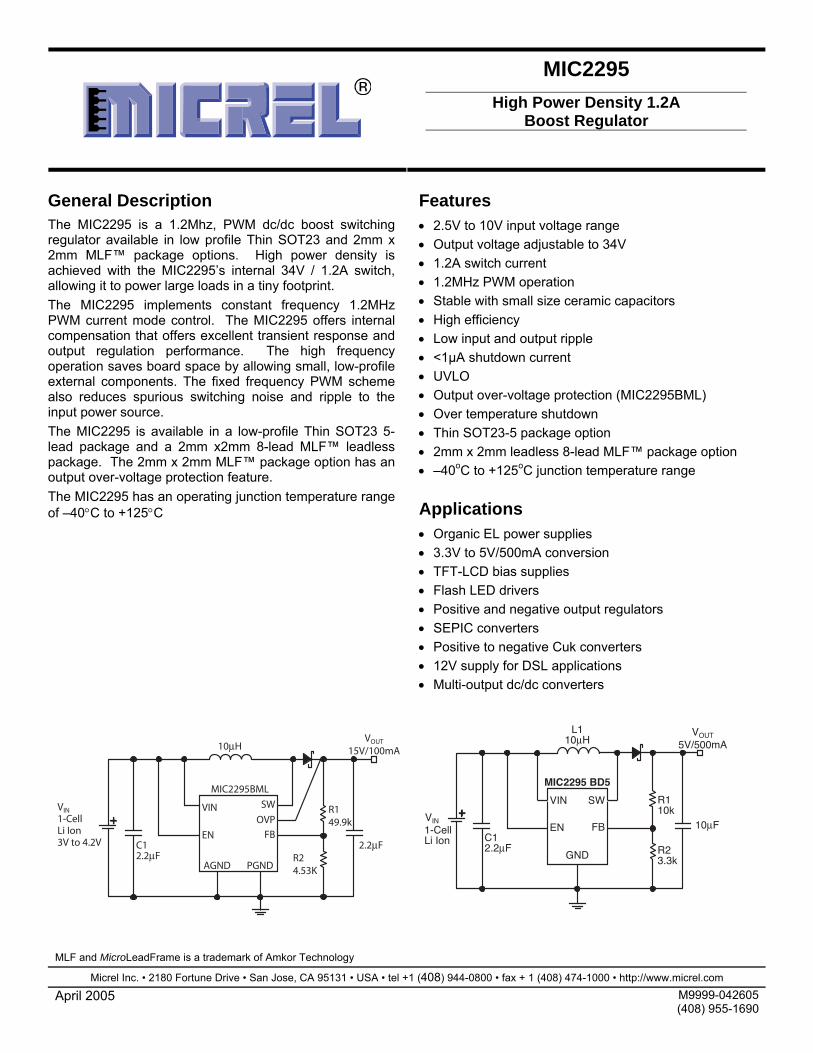
General Description The MIC2295 is a 1.2Mhz, PWM dc/dc boost switching regulator available in low profile Thin SOT23 and 2mm x 2mm MLF™ package options. High power density is achieved with the MIC2295’s internal 34V / 1.2A switch, allowing it to power large loads in a tiny footprint. The MIC2295 implements constant frequency 1.2MHz PWM current mode control. The MIC2295 offers internal compensation that offers excellent transient response and output regulation performance. The high frequency operation saves board space by allowing small, low-profile external components. The fixed frequency PWM scheme also reduces spurious switching noise and ripple to the input power source. The MIC2295 is available in a low-profile Thin SOT23 5-lead package and a 2mm x2mm 8-lead MLF™ leadless package. The 2mm x 2mm MLF™ package option has an output over-voltage protection feature. The MIC2295 has an operating junction temperature range of –40°C to +125°C
Features
• 2.5V to 10V input voltage range • Output voltage adjustable to 34V • 1.2A switch current • 1.2MHz PWM operation • Stable with small size ceramic capacitors • High efficiency • Low input and output ripple • <1µA shutdown current • UVLO • Output over-voltage protection (MIC2295BML) • Over temperature shutdown • Thin SOT23-5 package option • 2mm x 2mm leadless 8-lead MLF™ package option • –40oC to +125oC junction temperature range Applications • Organic EL power supplies • 3.3V to 5V/500mA conversion • TFT-LCD bias supplies • Flash LED drivers • Positive and negative output regulators • SEPIC converters • Positive to negative Cuk converters • 12V supply for DSL applications • Multi-output dc/dc converters
10µH
R24.53K
R149.9k
MIC2295BML
VIN VIN1-CellLi Ion3V to 4.2V
VOUT
15V/100mA
EN FB
AGND
C12.2µF
2.2µF
PGND
SWOVP
L110µH
R23.3k
R110k
MIC2295 BD5
VIN
1-CellLi Ion
VOUT
5V/500mA
EN
SW
FB
GND
VIN
C12.2µF
10µF
Micrel, Inc. MIC2295
April 2005 2 M9999-042605 (408) 955-1690
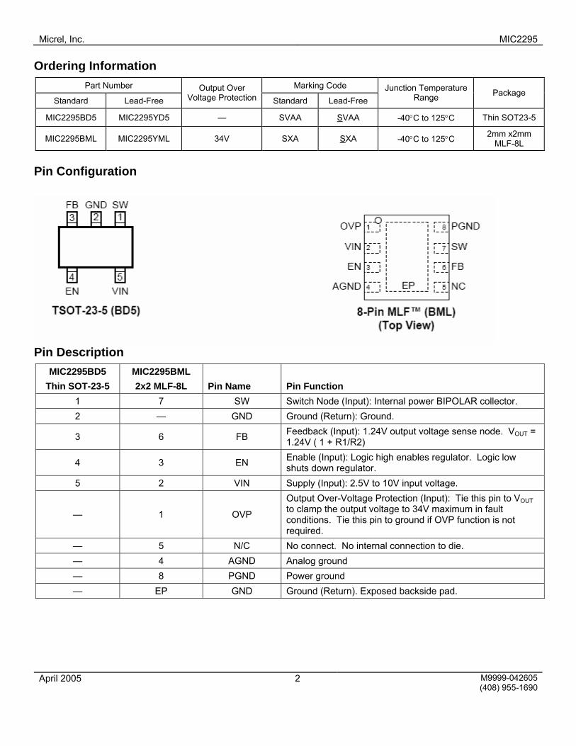
Ordering Information Part Number Marking Code
Standard Lead-Free Output Over
Voltage Protection Standard Lead-Free Junction Temperature
Range Package
MIC2295BD5 MIC2295YD5 — SVAA SVAA -40°C to 125°C Thin SOT23-5
MIC2295BML MIC2295YML 34V SXA SXA -40°C to 125°C 2mm x2mm MLF-8L
Pin Configuration
Pin Description
MIC2295BD5 Thin SOT-23-5
MIC2295BML 2x2 MLF-8L Pin Name Pin Function
1 7 SW Switch Node (Input): Internal power BIPOLAR collector. 2 — GND Ground (Return): Ground.
3 6 FB Feedback (Input): 1.24V output voltage sense node. VOUT = 1.24V ( 1 + R1/R2)
4 3 EN Enable (Input): Logic high enables regulator. Logic low shuts down regulator.
5 2 VIN Supply (Input): 2.5V to 10V input voltage.
— 1 OVP
Output Over-Voltage Protection (Input): Tie this pin to VOUT to clamp the output voltage to 34V maximum in fault conditions. Tie this pin to ground if OVP function is not required.
— 5 N/C No connect. No internal connection to die. — 4 AGND Analog ground — 8 PGND Power ground — EP GND Ground (Return). Exposed backside pad.
Micrel, Inc. MIC2295
April 2005 3 M9999-042605 (408) 955-1690
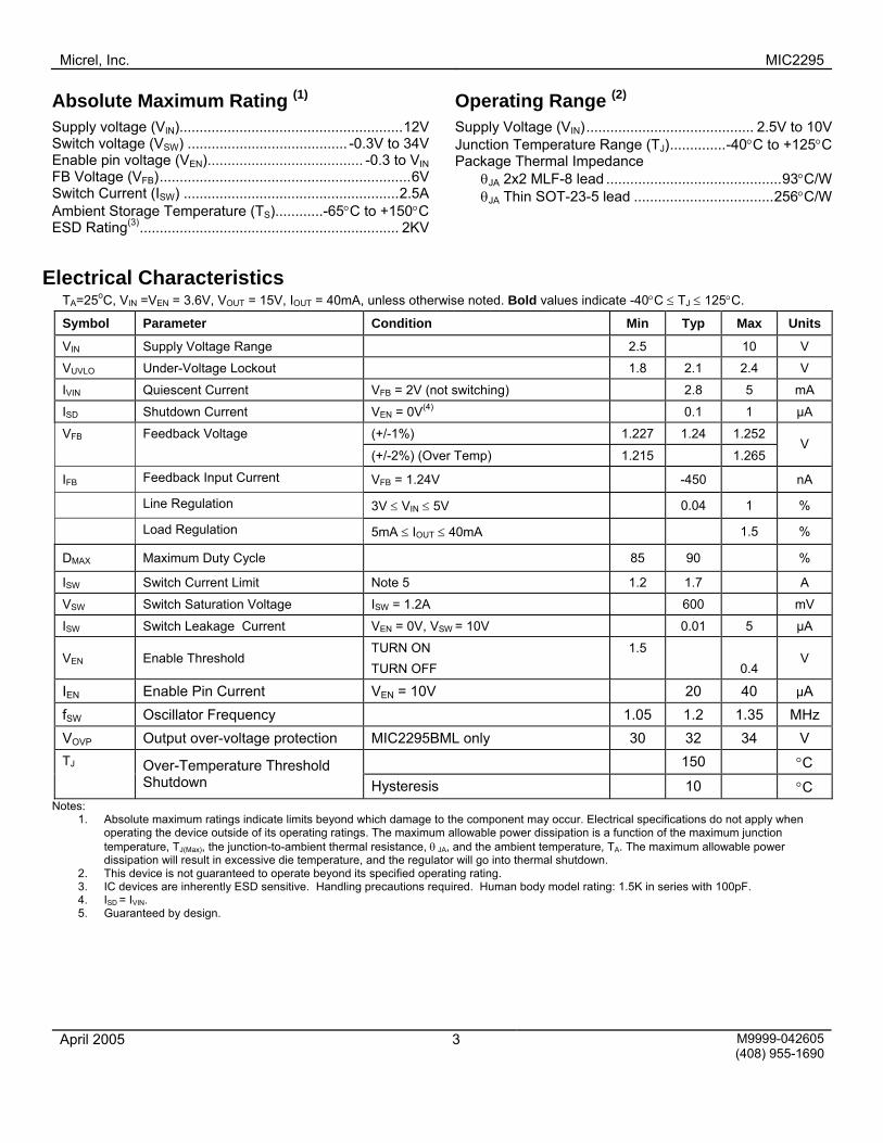
Absolute Maximum Rating (1) Supply voltage (VIN)........................................................12V Switch voltage (VSW) ........................................ -0.3V to 34V Enable pin voltage (VEN)....................................... -0.3 to VIN FB Voltage (VFB)...............................................................6V Switch Current (ISW) ......................................................2.5A Ambient Storage Temperature (TS)............-65°C to +150°C ESD Rating(3)................................................................. 2KV
Operating Range (2) Supply Voltage (VIN).......................................... 2.5V to 10V Junction Temperature Range (TJ)..............-40°C to +125°C Package Thermal Impedance θJA 2x2 MLF-8 lead ............................................93°C/W θJA Thin SOT-23-5 lead ...................................256°C/W
Electrical Characteristics TA=25oC, VIN =VEN = 3.6V, VOUT = 15V, IOUT = 40mA, unless otherwise noted. Bold values indicate -40°C ≤ TJ ≤ 125°C.
Symbol Parameter Condition Min Typ Max Units
VIN Supply Voltage Range 2.5 10 V
VUVLO Under-Voltage Lockout 1.8 2.1 2.4 V
IVIN Quiescent Current VFB = 2V (not switching) 2.8 5 mA
ISD Shutdown Current VEN = 0V(4) 0.1 1 µA
VFB Feedback Voltage (+/-1%) 1.227 1.24 1.252
(+/-2%) (Over Temp) 1.215 1.265 V
IFB Feedback Input Current VFB = 1.24V -450 nA
Line Regulation 3V ≤ VIN ≤ 5V 0.04 1 %
Load Regulation 5mA ≤ IOUT ≤ 40mA 1.5 %
DMAX Maximum Duty Cycle 85 90 %
ISW Switch Current Limit Note 5 1.2 1.7 A
VSW Switch Saturation Voltage ISW = 1.2A 600 mV
ISW Switch Leakage Current VEN = 0V, VSW = 10V 0.01 5 µA
VEN Enable Threshold TURN ON TURN OFF
1.5 0.4
V
IEN Enable Pin Current VEN = 10V 20 40 µA fSW Oscillator Frequency 1.05 1.2 1.35 MHz VOVP Output over-voltage protection MIC2295BML only 30 32 34 V
150 °C TJ Over-Temperature Threshold Shutdown Hysteresis 10 °C
Notes: 1. Absolute maximum ratings indicate limits beyond which damage to the component may occur. Electrical specifications do not apply when
operating the device outside of its operating ratings. The maximum allowable power dissipation is a function of the maximum junction temperature, TJ(Max), the junction-to-ambient thermal resistance, θ JA, and the ambient temperature, TA. The maximum allowable power dissipation will result in excessive die temperature, and the regulator will go into thermal shutdown.
2. This device is not guaranteed to operate beyond its specified operating rating. 3. IC devices are inherently ESD sensitive. Handling precautions required. Human body model rating: 1.5K in series with 100pF. 4. ISD = IVIN. 5. Guaranteed by design.

Micrel MIC2295
April 2005 4 M9999-042605 (408) 955-1690
Typical Characteristics MIC2295 -5V Output
30
35
40
45
50
55
60
65
70
75
80
0 100 200 300
Output Current
Vin=4V
Vin=5V
Vin=5.5V
VIN
EN
SW
FB
GND
MIC2295BML
1
2
3
4
5
VOUT = -5V @ 0.15A
4.7uF/
6.3V
CMHSH5-2L
10K
2.49K
1 F/
6.3V
VIN = 5V
R1
R2
L1 L2
C1 C2
C3
1uF/16V
L1 = Murata LQH32CN4R7M23
L2 = Murata LQH32CN4R7M23
+
-
1uF/
6.3V
C4
R3
10K
MIC6211
OVP
15V Short circuitprotected Boost
60
65
70
75
80
85
0 20 40 60 80 100OUTPUT CURRENT (mA)
Vin=2.5VVin=3V
VIN
EN
SW
FB
GND
MIC22951-Cell
Li Ion
1
2
3
4
5
VOUT = 15V / 50mA4.7µH
4.7µF/
25V
Sumida
CDRH4D18
160K
10K
10µF/
6.3V
CIN = JMK212BJ106MG (Taiyo Yuden)
0.1uF/
6.3V
Micrel MIC2295
April 2005 5 M9999-042605 (408) 955-1690
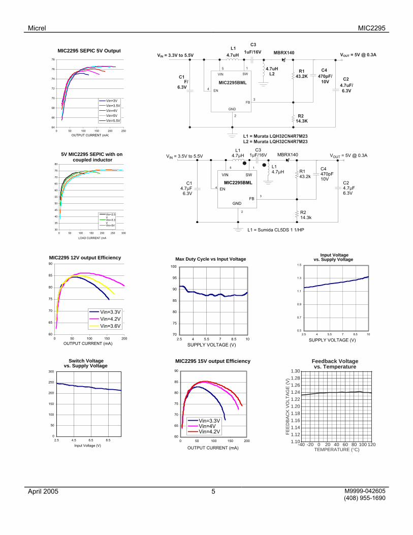
MIC2295 SEPIC 5V Output
64
66
68
70
72
74
76
78
0 50 100 150 200 250OUTPUT CURRENT (mA)
Vin=3VVin=3.5VVin=4VVin=5VVin=5.5V
VIN
EN
SW
FB
GND
MIC2295BML
1
2
3
4
5
VOUT = 5V @ 0.3A4.7uH
4.7uF/
6.3V
MBRX140
43.2K
14.3K
F/
6.3V
VIN = 3.3V to 5.5V
R1
R2
4.7uH
L1
L2C1 C2
C3
1uF/16V
L1 = Murata LQH32CN4R7M23
L2 = Murata LQH32CN4R7M23
470pF/
10V
C4
5V MIC2295 SEPIC with on
coupled inductor
30
35
40
45
50
55
60
65
70
75
80
0 50 100 150 200 250 300
LOAD CURRENT (mA
Vin=2.5VVin=3.3VVin=5V
1
2
3
4
5
VIN
EN
SW
FB
GND
MIC2295BML
VOUT = 5V @ 0.3AMBRX140VIN = 3.5V to 5.5V
R1
43.2k
R2
14.3k
L1
4.7µH
L1
4.7µH
C1
4.7µF
6.3V
C2
4.7µF
6.3V
C3
1µF/16V
L1 = Sumida CL5DS 1 1/HP
C4
470pF
10V
MIC2295 12V output Efficiency
60
65
70
75
80
85
90
0 50 100 150 200OUTPUT CURRENT (mA)
Vin=3.3VVin=4.2VVin=3.6V
Max Duty Cycle vs Input Voltage
70
75
80
85
90
95
100
2.5 4 5.5 7 8.5 10
SUPPLY VOLTAGE (V)
Input Voltage vs. Supply Voltage
0.5
0.7
0.9
1.1
1.3
1.5
2.5 4 5.5 7 8.5 10
SUPPLY VOLTAGE (V)
Switch Voltage vs. Supply Voltage
0
50
100
150
200
250
300
2.5 4.5 6.5 8.5
Input Voltage (V)
MIC2295 15V output Efficiency
60
65
70
75
80
85
90
0 50 100 150 200
OUTPUT CURRENT (mA)
Vin=3.3VVin=4VVin=4.2V
1.10
1.12
1.14
1.16
1.18
1.20
1.22
1.24
1.26
1.28
1.30
-40 -20 0 20 40 60 80 100 120
FE
ED
BA
CK
VO
LTA
GE
(V
)
TEMPERATURE (°C)
Feedback Voltagevs. Temperature
Micrel MIC2295
April 2005 6 M9999-042605 (408) 955-1690
0.8
0.9
1.0
1.1
1.2
1.3
1.4
-40 -20 0 20 40 60 80 100 120
FR
EQ
UE
NC
Y (
MH
z)
TEMPERATURE (°C)
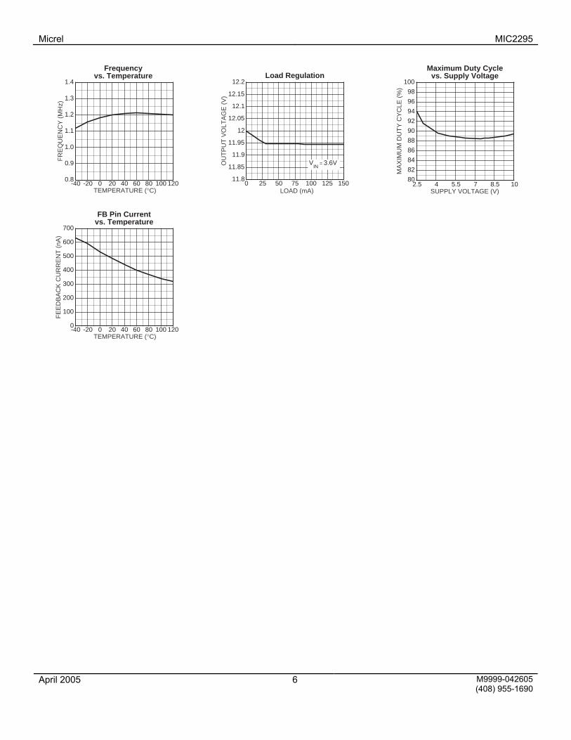
Frequencyvs. Temperature
11.8
11.85
11.9
11.95
12
12.05
12.1
12.15
12.2
0 25 50 75 100 125 150
OU
TP
UT
VO
LTA
GE
(V
)
LOAD (mA)
Load Regulation
VIN
= 3.6V
80
82
84
86
88
90
92
94
96
98
100
2.5 4 5.5 7 8.5 10
MA
XIM
UM
DU
TY
CY
CLE
(%
)
SUPPLY VOLTAGE (V)
Maximum Duty Cyclevs. Supply Voltage
0
100
200
300
400
500
600
700
-40 -20 0 20 40 60 80 100 120
FE
ED
BA
CK
CU
RR
EN
T (
nA)
TEMPERATURE (°C)
FB Pin Currentvs. Temperature

Micrel MIC2295
April 2005 7 M9999-042605 (408) 955-1690
Functional Characteristics Line Transient Response
Time (400µs/div)
OU
TP
UT
VO
LTA
GE
(1m
V/d
iv)
AC
-Cou
pled
INP
UT
VO
LTA
GE
(2V
/div
)
4.2V
3.2V
12VOUT 150mA Load
Switching Waveforms
Time (400ns/div)
OU
TP
UT
VO
LTA
GE
(50m
V/d
iv)
IND
UC
TOR
CU
RR
EN
T(5
00m
A/d
iv)
SW
ITC
H S
ATU
RAT
ION
(5V
/div
)
VSW
Output Voltage
3.6VIN
12VOUT
150mA
Inductor Current(10µH)
TIME (400µs/div.)
LOA
D C
UR
RE
NT
(2V
/div
.)O
UT
PU
T V
OLT
AG
E(5
V/d
iv.)
VIN = 3.6V
Enable Characteristics
VIN=3.6V
3.6VIN12VOUT
150mA Load
Micrel MIC2295
April 2005 8 M9999-042605 (408) 955-1690
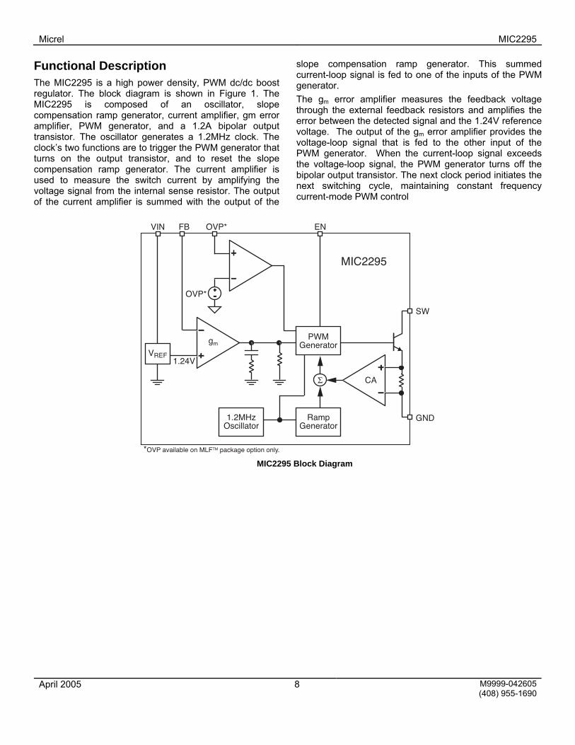
Functional Description The MIC2295 is a high power density, PWM dc/dc boost regulator. The block diagram is shown in Figure 1. The MIC2295 is composed of an oscillator, slope compensation ramp generator, current amplifier, gm error amplifier, PWM generator, and a 1.2A bipolar output transistor. The oscillator generates a 1.2MHz clock. The clock’s two functions are to trigger the PWM generator that turns on the output transistor, and to reset the slope compensation ramp generator. The current amplifier is used to measure the switch current by amplifying the voltage signal from the internal sense resistor. The output of the current amplifier is summed with the output of the
slope compensation ramp generator. This summed current-loop signal is fed to one of the inputs of the PWM generator. The gm error amplifier measures the feedback voltage through the external feedback resistors and amplifies the error between the detected signal and the 1.24V reference voltage. The output of the gm error amplifier provides the voltage-loop signal that is fed to the other input of the PWM generator. When the current-loop signal exceeds the voltage-loop signal, the PWM generator turns off the bipolar output transistor. The next clock period initiates the next switching cycle, maintaining constant frequency current-mode PWM control
GND
CA
PWMGenerator
RampGenerator
1.2MHzOscillator
SW
ENFB OVP*VIN
1.24V
*OVP available on MLFTM package option only.
gm
OVP*
Σ
VREF
MIC2295
MIC2295 Block Diagram
Micrel MIC2295
April 2005 9 M9999-042605 (408) 955-1690
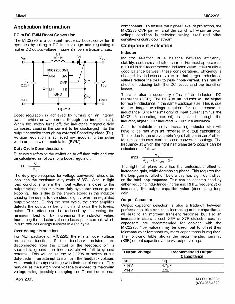
Application Information DC to DC PWM Boost Conversion The MIC2295 is a constant frequency boost converter. It operates by taking a DC input voltage and regulating a higher DC output voltage. Figure 2 shows a typical circuit.
L110mH
C210µF
R2
R1
MIC2288BML
VIN
VIN VOUT
EN
SW
FBGND
GND
OVP
GND
C12.2µF
D1
Figure 2
Boost regulation is achieved by turning on an internal switch, which draws current through the inductor (L1). When the switch turns off, the inductor’s magnetic field collapses, causing the current to be discharged into the output capacitor through an external Schottkey diode (D1). Voltage regulation is achieved my modulating the pulse width or pulse width modulation (PWM).
Duty Cycle Considerations Duty cycle refers to the switch on-to-off time ratio and can be calculated as follows for a boost regulator;
D = 1−VIN
VOUT
The duty cycle required for voltage conversion should be less than the maximum duty cycle of 85%. Also, in light load conditions where the input voltage is close to the output voltage, the minimum duty cycle can cause pulse skipping. This is due to the energy stored in the inductor causing the output to overshoot slightly over the regulated output voltage. During the next cycle, the error amplifier detects the output as being high and skips the following pulse. This effect can be reduced by increasing the minimum load or by increasing the inductor value. Increasing the inductor value reduces peak current, which in turn reduces energy transfer in each cycle.
Over Voltage Protection For MLF package of MIC2295, there is an over voltage protection function. If the feedback resistors are disconnected from the circuit or the feedback pin is shorted to ground, the feedback pin will fall to ground potential. This will cause the MIC2295 to switch at full duty-cycle in an attempt to maintain the feedback voltage. As a result the output voltage will climb out of control. This may cause the switch node voltage to exceed its maximum voltage rating, possibly damaging the IC and the external
components. To ensure the highest level of protection, the MIC2295 OVP pin will shut the switch off when an over-voltage condition is detected saving itself and other sensitive circuitry downstream.
Component Selection Inductor Inductor selection is a balance between efficiency, stability, cost, size and rated current. For most applications a 10µH is the recommended inductor value. It is usually a good balance between these considerations. Efficiency is affected by inductance value in that larger inductance values reduce the peak to peak ripple current. This has an effect of reducing both the DC losses and the transition losses. There is also a secondary effect of an inductors DC resistance (DCR). The DCR of an inductor will be higher for more inductance in the same package size. This is due to the longer windings required for an increase in inductance. Since the majority of input current (minus the MIC2295 operating current) is passed through the inductor, higher DCR inductors will reduce efficiency. Also, to maintain stability, increasing inductor size will have to be met with an increase in output capacitance. This is due to the unavoidable “right half plane zero” effect for the continuous current boost converter topology. The frequency at which the right half plane zero occurs can be calculated as follows;
Frhpz =VIN
2
VOUT ×L × IOUT × 2π
The right half plane zero has the undesirable effect of increasing gain, while decreasing phase. This requires that the loop gain is rolled off before this has significant effect on the total loop response. This can be accomplished by either reducing inductance (increasing RHPZ frequency) or increasing the output capacitor value (decreasing loop gain).
Output Capacitor Output capacitor selection is also a trade-off between performance, size and cost. Increasing output capacitance will lead to an improved transient response, but also an increase in size and cost. X5R or X7R dielectric ceramic capacitors are recommended for designs with the MIC2295. Y5V values may be used, but to offset their tolerance over temperature, more capacitance is required. The following table shows the recommended ceramic (X5R) output capacitor value vs. output voltage.
Output Voltage Recommended Output Capacitance
<6V 10µF <16V 4.7µF <34V 2.2µF

Micrel MIC2295
April 2005 10 M9999-042605 (408) 955-1690
Diode Selection The MIC2295 requires an external diode for operation. A Schottkey diode is recommended for most applications due to their lower forward voltage drop and reverse recovery time. Ensure the diode selected can deliver the peak inductor current and the maximum reverse voltage is rated greater than the output voltage.
Input Capacitor A minimum 1µF ceramic capacitor is recommended for designing with the MIC2295. Increasing input capacitance will improve performance and greater noise immunity on the source. The input capacitor should be as close as possible to the inductor and the MIC2295, with short traces for good noise performance.
Feedback Resistors The MIC2295 utilizes a feedback pin to compare the output to an internal reference. The output voltage is adjusted by selecting the appropriate feedback resistor values. The desired output voltage can be calculated as follows;
VOUT = VREF ×R1R2
+1⎛ ⎝ ⎜
⎞ ⎠ ⎟
Where VREF is equal to 1.24V.
Duty-Cycle The MIC2295 is a general-purpose step up DC-DC converter. The maximum difference between the input voltage and the output voltage is limited by the maximum duty-cycle (Dmax) of the converter. In the case of MIC2295, DMAX = 85%. The actual duty cycle for a given application can be calculated as follows:
D = 1−VIN
VOUT
The actual duty-cycle, D, cannot surpass the maximum rated duty-cycle, Dmax.
Output Voltage Setting The following equation can be used to select the feedback resistors R1 and R2 (see figure 1).
R1 = R2 ⋅VOUT
1.24V−1
⎡ ⎣ ⎢
⎤ ⎦ ⎥
A high value of R2 can increase the whole system efficiency, but the feedback pin input current (IFB) of the gm operation amplifier will affect the output voltage. The R2 resistor value must be less than or equal to 5kΩ (R2 ≤ 5 kΩ).
Inductor Selection In MIC2295, the switch current limit is 1.2A. The selected inductor should handle at least 1.2A current without saturating. The inductor should have a low DC resistor to minimize power losses. The inductor’s value can be 4.7µH to 10µH for most applications.
Capacitor Selection Multi-layer ceramic capacitors are the best choice for input and output capacitors. They offer extremely low ESR, allowing very low ripple, and are available in very small, cost effective packages. X5R dielectrics are preferred. A 4.7µF to 10µF output capacitor is suitable for most applications.
Diode Selection For maximum efficiency, Schottky diode is recommended for use with MIC2295. An optimal component selection can be made by choosing the appropriate reverse blocking voltage rating and the average forward current rating for a given application. For the case of maximum output voltage (34V) and maximum output current capability, a 40V / 1A Schottky diode should be used.
Open-Circuit Protection For MLF package option of MIC2295, there is an output over-voltage protection function that clamps the output to below 34V in fault conditions. Possible fault conditions may include: if the device is configured in a constant current mode of operation and the load opens, or if in the standard application the feedback resistors are disconnected from the circuit. In these cases the FB pin will pull to ground, causing the MIC2295 to switch with a high duty-cycle. As a result, the output voltage will climb out of regulation, causing the SW pin to exceed its maximum voltage rating and possibly damaging the IC and the external components. To ensure the highest level of safety, the MIC2295 has a dedicated pin, OVP, to monitor and clamp the output voltage in over-voltage conditions. The OVP function is offered in the 2mm x 2mm MLF-8L package option only. To disable OVP function, tie the OVP pin to ground

Micrel MIC2295
April 2005 11 M9999-042605 (408) 955-1690
L14.7µH
C210µF16V
R21.87k
R15.62k
MIC2295BML
VIN
VIN3V to 4.2V
VOUT5V @ 400mA
EN
SW
FBGND
GND
OVP
GND
C14.7µF
6.3V
D1
470 pF
3.3VIN to 5VOUT @ 400mA
L110µH
C24.7µF16V
R25k
R131.6k
MIC2295BML
VIN
VIN3V to 4.2V
VOUT9V @ 180mA
EN
SW
FBGND
GND
OVP
GND
C12.2µF
10V
D1
3VIN - 4.2VIN to 9VOUT @ 180mA
L110µH
C24.7µF16V
R25k
R143.2k
MIC2295BML
VIN
VIN3V to 4.2V
VOUT12V @ 120mA
EN
SW
FBGND
GND
OVP
GND
C12.2µF
10V
D1
3VIN - 4.2Vin to 12VOUT @ 120mA
L110µH
C24.7µF16V
R25k
R143.2k
MIC2295BML
VIN
VIN3V to 5V
VOUT12V @ 120mA
EN
SW
FBGND
GND
OVP
GND
C12.2µF
10V
D1
3VIN – 5VIN to 12VOUT @ 120mA
L110µH
C22.2µF16V
R25k
R143.2k
MIC2295BML
VIN
VIN3V to 5V
VOUT12V @ 120mA
EN
SW
FBGND
GND
OVP
GND
C12.2µF
10V
D1
3VIN – 5VIN to 12VOUT @ 120mA
L14.7µH
C24.7µF16V
R21.87k
R15.62k
MIC2295BML
VIN
VIN3V to 4.2V
VOUT5V @ 400mA
EN
SW
FBGND
GND
OVP
GND
C14.7µF6.3V
D1
470 pF
3VIN - 4.2VIN to 5VOUT @ 400mA
L110µH
C24.7µF16V
R25k
R143.2k
MIC2295BML
VIN
VIN3V to 5V
VOUT12V @300mA
EN
SW
FBGND
GND
OVP
GND
C12.2µF
10V
D1
3VIN to 5VIN to 12VOUT @ 300mA
L110µH
C22.2µF25V
R25k
R143.2k
MIC2295BML
VIN
VIN 5V
VOUT24V@80mA
EN
SW
FBGND
GND
OVP
GND
C12.2µF
10V
D1
5VIN to 24VOUT @ 80mA
Micrel MIC2295
April 2005 12 M9999-042605 (408) 955-1690
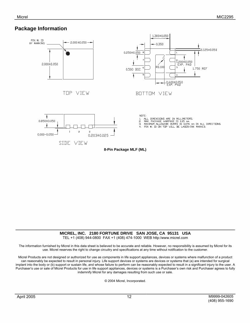
Package Information
8-Pin Package MLF (ML)
MICREL, INC. 2180 FORTUNE DRIVE SAN JOSE, CA 95131 USA TEL +1 (408) 944-0800 FAX +1 (408) 474-1000 WEB http:/www.micrel.com
The information furnished by Micrel in this data sheet is believed to be accurate and reliable. However, no responsibility is assumed by Micrel for its
use. Micrel reserves the right to change circuitry and specifications at any time without notification to the customer.
Micrel Products are not designed or authorized for use as components in life support appliances, devices or systems where malfunction of a product can reasonably be expected to result in personal injury. Life support devices or systems are devices or systems that (a) are intended for surgical
implant into the body or (b) support or sustain life, and whose failure to perform can be reasonably expected to result in a significant injury to the user. A Purchaser’s use or sale of Micrel Products for use in life support appliances, devices or systems is a Purchaser’s own risk and Purchaser agrees to fully
indemnify Micrel for any damages resulting from such use or sale.
© 2004 Micrel, Incorporated.