micro fuel cell fabrication technologies -...
TRANSCRIPT

9HSTFMG*affjda+
ISBN 978-952-60-5593-0 ISBN 978-952-60-5594-7 (pdf) ISSN-L 1799-4934 ISSN 1799-4934 ISSN 1799-4942 (pdf) Aalto University School of Chemical Technology Department of Materials Science and Engineering www.aalto.fi
BUSINESS + ECONOMY ART + DESIGN + ARCHITECTURE SCIENCE + TECHNOLOGY CROSSOVER DOCTORAL DISSERTATIONS
Aalto-D
D 2
9/2
014
Gianm
ario Scotti M
icro fuel cell fabrication technologies A
alto U
nive
rsity
Department of Materials Science and Engineering
Micro fuel cell fabrication technologies
Gianmario Scotti
DOCTORAL DISSERTATIONS

Aalto University publication series DOCTORAL DISSERTATIONS 29/2014
Micro fuel cell fabrication technologies
Gianmario Scotti
A doctoral dissertation completed for the degree of Doctor of Science (Technology) to be defended, with the permission of the Aalto University School of Chemical Technology, at a public examination held at the Large Seminar Hall in Micronova, Tietotie 3, 02150 Espoo (Finland) on the 9th of May 2014 at 12:00.
Aalto University School of Chemical Technology Department of Materials Science and Engineering Microfabrication Group

Supervising professor Professor Sami Franssila Thesis advisors Professor Sami Franssila Docent Tanja Kallio Preliminary examiners Dr. María Neus Sabaté Vizcarra, Instituto de Microelectrónica de Barcelona, IMB-CNM (CSIC), Spain Dr. Steve Arscott, University of Lille, France Opponent Professor Chang-Jin Kim, UCLA, USA
Aalto University publication series DOCTORAL DISSERTATIONS 29/2014 © Gianmario Scotti ISBN 978-952-60-5593-0 ISBN 978-952-60-5594-7 (pdf) ISSN-L 1799-4934 ISSN 1799-4934 (printed) ISSN 1799-4942 (pdf) http://urn.fi/URN:ISBN:978-952-60-5594-7 Unigrafia Oy Helsinki 2014 Finland
Abstract Aalto University, P.O. Box 11000, FI-00076 Aalto www.aalto.fi
Author Gianmario Scotti Name of the doctoral dissertation Micro fuel cell fabrication technologies Publisher Unit Department of Materials Science and Engineering
Series Aalto University publication series DOCTORAL DISSERTATIONS 29/2014
Field of research Microelectromechanical Systems
Manuscript submitted 6 February 2014 Date of the defence 9 May 2014
Permission to publish granted (date) 11 February 2014 Language English
Monograph Article dissertation (summary + original articles)
Abstract Fuel cells are established devices for high efficiency conversion of chemical into electrical
energy. Microfabricated fuel cells (MFC) promise higher energy density compared to rechargeable batteries currently used in portable applications (mobile phones, tablets, laptops etc.). In this work new fabrication technologies have been developed to make MFCs more viable alternatives to batteries. Like other microfluidic devices, MFCs can be fabricated using a number of different techniques, each with its specific advantage and drawback. In this doctoral dissertation, three microfabrication technologies have been used to produce MFCs: deep reactive ion etching (DRIE) of silicon, laser ablation of silicon and bulk aluminium wet etching. In all cases, the substrate acted as current collector, so good conductivity was important.
The science produced is of value beyond the scope of fuel cells alone: integration of black silicon with microfluidic devices, rapid prototyping of microfluidic devices with laser ablation, and using aluminium as a cheap (and cheap to micromachine) but sturdy material for microfluidics. In the case of DRIE-fabricated micro fuel cells, black silicon was studied as both a simple integrated gas diffusion layer (GDL), and as promoter of galvanic contact between highly-doped silicon and carbon felt GDLs. Integrating a GDL into a MFC increases the cost of the device, but this increase is minimized using black silicon. Creating tens to hundreds of micrometer thick GDLs proved to be difficult; using black silicon to integrate a commercial carbon cloth GDL easily solves this problem. The work on laser-ablated micro fuel cells yielded useful results for microfabricators that want to use picosecond laser ablation in microfluidics and other MEMS fields; the technique of picosecond laser ablation of silicon developed in this study enables the creation of ~60 micrometer deep channels at an overall speed of 15 mm/s and very low induced stress. The method enables the microfabrication of channels and through-hole gas inlets in the same process step, without the need of lithography. The bulk-aluminium MFCs produced very high current density (1.1 A/cm2) and power density (228 mW/cm2), but the study of bulk-aluminium microfabrication also offers detailed guidelines for microfabrication of other aluminium microfluidic devices.
Keywords DRIE, silicon, aluminium, laser ablation, micro fuel cells
ISBN (printed) 978-952-60-5593-0 ISBN (pdf) 978-952-60-5594-7
ISSN-L 1799-4934 ISSN (printed) 1799-4934 ISSN (pdf) 1799-4942
Location of publisher Helsinki Location of printing Helsinki Year 2014
Pages 150 urn http://urn.fi/URN:ISBN:978-952-60-5594-7


i
Preface
When I was a kid, 8 or 9 years old, I knew for sure that when I grow up, I will be a scientist. Science, or
my desire to be a scientist, wasn’t something I would reflect upon very deeply. Rather, science was
something I was passionate about, and to this day I still am. First to captivate my attention was chemistry,
and I did make a lot of interesting experiments at home and outside. I was mostly safe, apart from a few
experiments that could have caused me some bodily harm (but did not).
Later I fell in love with electrical engineering, and later still, with electronics. I have vivid memories of
building a two-transistor relaxation multivibrator using a connector block, and experimenting with
various values of capacitors and resistors. Eventually I studied and then graduated as an electrical
engineer with a major in electronics.
Unfortunately, after graduating I needed a job with some urgency, so I took a position as computer
network engineer, and worked in the IT field for the next 12 years. Even though I tried getting a job as a
researcher, my many attempts remained fruitless. Until the day that I undertook my second master’s
studies, at TKK (now Aalto), and after a few exams passed with highest marks, met my adviser Prof.
Sami Franssila, who looked at what is in my head and evaluated my potential, rather than to look at my
employment record. And thus begun my adventure as an adult scientist.
Working as a scientist has been a lot of fun, and while it is not the greatest career in financial terms nor
does it offer good job security, I still would not do anything else. It is the job where creativity and insight
matter more than in any other field of human activity. And creativity and insight is what I have to offer.
My companions in this great adventure, and the people to whom I owe gratitude, are the many colleagues
I met during the past several years, but I want to point out Sami, whose ideas were almost as numerous
and creative as my own, and Petri Kanninen, co-author of all the papers I present in this thesis. Petri and I
have spent many hours in the physical chemistry lab, characterizing the fuel cells I would fabricate in
Micronova’s cleanroom. We did many un-orthodox experiments together, some of which were successful
and all of which were rewarding.
Finally, I want to thank my mother for raising me with all her love, my wife for putting up with me, and
my son Sailom for being the most wonderful and caring creature in the universe, and who gives purpose
to everything I do.

ii
Contents
1. Introduction...................................................................................................................................................... 1
1.1. Motivation ................................................................................................................................................ 1
1.2. Microfabrication....................................................................................................................................... 2
1.3. Micro fuel cells ........................................................................................................................................ 3
2. Microfabrication technologies ........................................................................................................................ 8
2.1. Optical lithography ................................................................................................................................ 11
2.2. Etching .................................................................................................................................................... 12
2.2.1 Isotropic etching .............................................................................................................................. 15
2.2.2 Anisotropic plasma etching – reactive ion etching (RIE) ............................................................. 16
2.2.3 Anisotropic wet etching................................................................................................................... 21
2.3. Thin-film technologies........................................................................................................................... 23
2.3.1 Evaporation and sputtering ............................................................................................................. 24
2.3.2 Chemical vapor deposition (CVD) ................................................................................................. 27
2.3.3 Atomic layer deposition (ALD) ...................................................................................................... 29
2.3.4 Electroplating ................................................................................................................................... 29
2.4. Laser ablation ......................................................................................................................................... 30
2.5 Other technologies for micro fuel cells ................................................................................................. 36
3. Fuel cells ........................................................................................................................................................ 39
3.1. Fuel cell operation.................................................................................................................................. 39
3.2. Fuel cell taxonomy ................................................................................................................................. 41
3.2.1 Proton exchange membrane fuel cells (PEMFC) .......................................................................... 42
3.2.2 Alkaline (AFC) and alkaline membrane fuel cells (AMFC)......................................................... 46
3.2.3 Phosphoric acid fuel cells (PAFC) ................................................................................................. 47
3.2.4 Molten carbonate fuel cells (MCFC) .............................................................................................. 48
3.2.5 Solid oxide fuel cell (SOFC) ........................................................................................................... 49
3.2.6 Laminar flow fuel cell (LFFC) ....................................................................................................... 50
3.3 Fuel cell characterization ........................................................................................................................ 52
3.3.1 Open circuit voltage and polarization curves ................................................................................. 53
3.3.2 Cyclic voltammetry (CV) ................................................................................................................ 57
3.3.3 Chronoamperometric and -potentiometric measurements ............................................................ 58
3.3.4 Electrochemical impedance spectroscopy (EIS)............................................................................ 59
iii
4. Novel approaches to microfabrication of fuel cells .................................................................................... 60
4.1 MFCs with silicon nanograss (publications I, II and III) ..................................................................... 60
4.1.1 MFCs with silicon nanograss as gas diffusion layer (I) ................................................................ 61
4.1.2 Stackable silicon MFC (II) .............................................................................................................. 65
4.1.3 Silicon MFCs with silicon nanograss for integration of commercial gas diffusion layer (III) ... 68
4.2 Laser-ablated silicon MFCs (publication IV)........................................................................................ 71
4.3 Bulk-aluminium MFCs (publication V) ................................................................................................ 75
5. Conclusions and outlook ............................................................................................................................... 79
References .......................................................................................................................................................... 82

iv
List of Publications
[I] Gianmario Scotti, Petri Kanninen, Maija Mäkinen, Tanja Kallio, and Sami Franssila, "Siliconnanograss as micro fuel cell gas diffusion layer," Micro Nano Lett., vol. 5, pp. 382-385, 2010.
[II] Gianmario Scotti, Petri Kanninen, Tanja Kallio, and Sami Franssila, "A micro fuel cell stack withoutinterconnect overhead - macro world-like stacks in MEMS," in 21st Micromechanics and Microsystems Europe (MME2010), Enschede, The Netherlands, 2010, pp. 161-164.
[III] Gianmario Scotti, Petri Kanninen, Tanja Kallio, and Sami Franssila, "Integration of carbon felt gasdiffusion layers in silicon micro fuel cells," J. Micromech. Microeng., vol. 22, no. 9, p. 094006, 2012.
[IV] Gianmario Scotti, Daniel Trusheim, Petri Kanninen, Denys Naumenko, Malte Schulz-Ruhtenberg,Valentinas Snitka, Tanja Kallio, and Sami Franssila, "Picosecond laser ablation for silicon micro fuelcell fabrication," J. Micromech. Microeng., vol. 23, no. 5, p. 055021, 2013.
[V] Gianmario Scotti, Petri Kanninen, Tanja Kallio, and Sami Franssila, "Bulk-AluminumMicrofabrication for Micro Fuel Cells," J. Microelectromech. S., DOI 10.1109/JMEMS.2013.2274592
Author’s contribution
In publications [I]-[V], the author was responsible for the design and fabrication of all the samples and thedesign of the experiments, as well as some of the experimental work in the physical chemistry lab. Theauthor researched the relevant literature and wrote the majority of the articles’ content.

1
1. Introduction
1.1. Motivation
In 1952 Geoffrey Dummer presented, for the first time, the concept of integrated circuits [1], and in 1958,
Jack Kilby built and demonstrated such a device. This is when the idea of industrial solid-state
miniaturization technology was born. Next year, Richard Feynman gave one of the most famous lectures
of recent times, titled “There’s Plenty of Room at the Bottom.” This lecture is rightly considered the
milestone that introduced the concepts of nanotechnology and microfabrication. Back then, Feynman
could not have had knowledge of technical tools and methods that would make his vision a reality, yet his
vision was very clear and inspiring. Some of the things he envisioned have only become reality several
decades or even half a century later.
The subject of microtechnology was historically mostly centered around silicon semiconductors, starting
with Robert Noyce’s 1959 patent filing for a silicon integrated circuit [2]. However, an increasingly large
volume of work has been dedicated to microfabrication of devices that were not purely electronic —
micro-electromechanical systems (MEMS) — with a jump in activity at the end of the 1960’s [3] and
beginning of the 1970’s [4] [5]. Several types of sensors and actuators were created by micromachining
[6], leading to MEMS becoming a new scientific discipline in itself. MEMS researchers have produced a
large variety of devices: magnetic, flow, thermal, optical and chemical sensors, gyroscopes,
accelerometers, capacitive, thermal and electromagnetic actuators, micromirrors, gas chromatography
microcolumns, microreactors, and (the topic of this dissertation) micro fuel cells [7] [8] [9] [10] [11]. The
latter three are the subjects of a MEMS sub-discipline called microfluidics.
The conversion of energy has played an essential role in the history of science and technology, and human
activity in general. It was the enabler, for instance, of the industrial revolution. Energy conversion can be
achieved with heat engines such as the steam engine and the internal combustion engine (thermal to
mechanical), and more recently fuel cells (chemical to electrical) and energy harvesters (mechanical to
electrical). The latter systems are amenable to miniaturization and applicable to portable electronic

2
devices such as mobile phones, laptops, tablets, and digital cameras. The advantage of fuel cells in
particular is the large energy density of the fuels (hydrogen, methanol, ethanol and other alcohols) and
also their relative abundance. Microfabricated fuel cells — micro fuel cells (MFCs) — require
micro/nanofabrication technologies, specifically microfluidics, and are prime candidates to replace
traditional batteries in mobile applications.
1.2. Microfabrication
In MEMS, the starting point in creating a microdevice is usually a wafer. By far the most popular wafer
material is monocrystalline silicon, but glass wafers are also very important for MEMS. Other wafer
materials encountered in MEMS research are sapphire, quartz, polymethyl methacrylate (PMMA). These
substrate materials can be micromachined using chemicals, plasma, laser beams, ion beams or a
combination of these, to form 2D or 3D features. On the substrate material, thin films are often deposited
– metals (aluminium, copper, gold, chromium, platinum) ceramics (SiO2, Si3N4, Al2O3, TiO2), polymers
(polyimide, PTFE). These films can then be micromachined to form 2D structures, or, when released, 3D
structures such as beams, bridges and diaphragms.
Both the bulk of the substrate and the deposited films are commonly micromachined by first transferring a
pattern from a previously-prepared photographic mask onto a photosensitive material. Once the
photosensitive material is photo-patterned, it protects the underlying substrate and/or thin film from the
subsequent chemical or ion etching, ion implantation or metallization. The process of pattern transfer
from the mask to the photoresist is called lithography. Alternatively, the bulk and the deposited films can
be micromachined directly with a computer-controlled laser beam or focused ion beam.
The MEMS devices need to be protected from the natural environment. This protection can be achieved
by bonding a second wafer on top of the substrate, effectively capping it. Bonding is also used to achieve
higher complexity of MEMS devices: the capping wafer may also contain microfabricated structures
which inter-operate with those in the substrate. Multi-level bonding is possible and sometimes used in
MEMS.
Figure 1.1 shows a 3D model of a microfluidic chip microfabricated from silicon, with thin catalyst film
in the channels, and bonded with a capping glass wafer [12]. The figure shows a cross-sectional view
obtained along the dashed line in the inset. This microreactor was used for propene hydrogenation

3
catalyzed by the platinum film deposited in the channels. The channels were etched in the silicon wafer
using plasma etching. Plasma etching was used also to create the inlet holes. This etch step required back-
side alignment and lithography. The metal film was deposited by physical vapor deposition, and it is
about 100 nm thick.
Fig. 1.1: 3D model of microfluidic microreactor chip used in [12]. The inset in the bottom left showswhere the cross section was taken. The channels are 50 x 50 μm2 in cross section, and 10 mm long.
1.3. Micro fuel cells
Fuel cells are among many of the devices that have been scaled down with the help of microfabrication.
Fuel cells are electrochemical devices that convert energy from the chemical to the electrical world. That
is, they produce electrical energy by reacting a fuel (gaseous or liquid) with an oxidant, in an
electrochemical process. In this sense, fuel cells are similar to primary batteries, but with the distinction
that once the reactants are exhausted, a battery will stop producing electrical energy, whereas a fuel cell
will continue working until fuel and oxidant are provided – in theory indefinitely. The conversion in a
fuel cell is characterized by high efficiency compared to thermodynamic systems like combustion
engines. This is because of the limitations imposed by the laws of thermodynamics to which combustion
engines must adhere.
Fuel cells were invented in 1838 by W. R. Grove: his apparatus used a hydrogen anode and oxygen
cathode, and an aqueous solution of sulfuric acid. However, it was only in the 1960’s, thanks to the

4
advent of solid electrolytes, that fuel cells found practical use – namely, as power sources for space
probes.
Figure 1.2 illustrates the principle of operation of a typical fuel cell. In this example, hydrogen gas is used
as fuel and it is introduced from the anode side of an electrolytic membrane. On the cathode side, air is
introduced, and it is the oxygen present in the air that is the oxidizing agent. Hydrogen dissociates on the
surface of the electrolyte and the hydrogen atoms lose their electrons (oxidation), which then close the
electric circuit outside the cell. H+ cations travel through the electrolyte to the cathode where they
combine with the reduced oxygen O- to form water.
Fig. 1.2: Illustration of the principle of operation of a typical fuel cell: hydrogen (fuel) molecules losetheir electrons which travel through the external circuit where energy is consumed.
FCs are used as stationary units for residential primary and backup power generation, or as truck-portable
generators for temporary and remote locations. Since the 1990’s, FCs have been used in the automotive
industry for powering electric vehicles, such as electric cars, buses and forklifts. These efforts were
motivated by the low emission of harmful gases of these vehicles, which is especially important for
forklifts, often used in closed spaces.
Micro fuel cells (MFC) [11] [13] are microfluidic devices that function in a similar way to normal-sized
fuel cells, but have microscopic features and are fabricated using MEMS techniques. Just as with normal
fuel cells, MFCs produce electric power from liquid or gaseous fuels. The motivation for research in
MFCs is their potential as a replacement for rechargeable batteries in portable devices. For instance, a

5
typical Li-ion rechargeable battery has an energy density of less than 100 Wh kg-1, while methanol has
5500 Wh kg-1 and compressed hydrogen (including container weight) has 500-1000 Wh kg-1 [13].
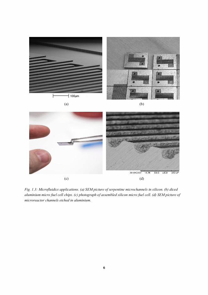
Figure 1.3 shows images of micro fuel cells illustrating their typical features: (a) Scanning electron
microscopy (SEM) image of a serpentine flowfield, from a silicon micro fuel cell (MFC) chip [I]. The
channels are 30 μm deep and 50 μm wide. (b) Diced aluminium MFC chips (stackable design, [II]). Each
chip is 14 x 14 mm2 in size. (c) An assembled silicon MFC. The total thickness (consisting of two chips
and a membrane-electrode assembly (MEA)) is 1.1 mm. (d) SEM image of microchannels, 50 μm deep,
etched in aluminium, part of a microreactor (the sample was sawn off for the purpose of
microphotography using the method described in [V]).
6
(a) (b)
(c) (d)
Fig. 1.3: Microfluidics applications. (a) SEM picture of serpentine microchannels in silicon. (b) dicedaluminium micro fuel cell chips. (c) photograph of assembled silicon micro fuel cell. (d) SEM picture ofmicroreactor channels etched in aluminium.
7
The research described in this thesis contributes to the advancement in micro fuel cell research, as well as
general microfabrication with silicon and aluminium as bulk materials. The main goals for the micro fuel
cells were to produce devices with high current and power densities, and to make them economical for
production. Performance improvements were obtained through integration of commercial gas diffusion
layer with microfluidic chips, and with the use of aluminium as an alternative bulk microfabrication
material. Production economies were obtained by limiting the number of microfabrication steps, the use
of silicon nanograss as gas diffusion layer, and the use of chromium instead of noble metals whenever
possible. Using aluminium alloys instead of silicon for bulk micromachining also decreases the unit price.
The key technologies used were silicon deep reactive ion etching (DRIE), physical vapor deposition of
thin films, laser ablation of silicon and wet etching of thin films and bulk aluminium. The thesis includes
an introductory section on microfabrication and a section on fuel cell technology, with a review of
publications pertaining to both theoretical and practical research in microfabrication and fuel cells, with
an emphasis on micro fuel cells. Finally, the author’s contributions are presented by describing the
various scientific ideas that comprise his published work in the field of micro fuel cells, mostly through
the perspective of microfabrication.

8
2. Microfabrication technologies
The word “microfabrication” can be defined as the production of miniature devices, with some of the
features being in the micrometer range. The technologies used in microfabrication derive from the
semiconductor industry, where miniature transistors, resistors and other electronic components are
produced at the microscale. In MEMS, these technologies have been extended to produce electrical,
mechanical, fluidic, and electromechanical microdevices; virtually all technologies used in integrated
circuit (IC) fabrication are also used in MEMS: In contrast to MEMS, semiconductor manufacturing does
not deal with mechanical, electromechanical or fluidic sensors and actuators. MEMS, on the other hand,
may concern itself also with integration of semiconductor components with electromechanical ones.
Integrated circuits are made chiefly from silicon, and silicon oxide has been an excellent passivation and
dielectric layer in ICs. Microfabrication techniques focused on these materials are mature and it is no
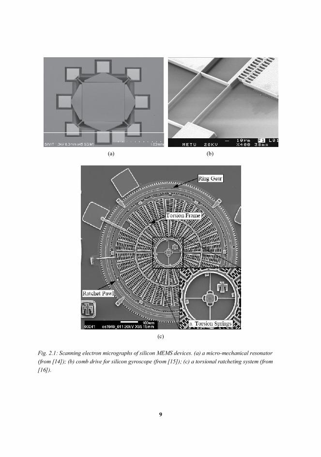
surprise therefore, that silicon microfabrication techniques are often used in MEMS. Figure 2.1 presents
SEM images of a few MEMS devices microfabricated from silicon: (a) shows a micro-mechanical
resonator fabricated from a silicon-on-insulator (SOI) wafer [14]; in (b) we can see a comb drive for a
monocrystalline silicon gyroscope [15]; in (c) we can see a torsional ratcheting system.
9
(a) (b)
(c)
Fig. 2.1: Scanning electron micrographs of silicon MEMS devices. (a) a micro-mechanical resonator(from [14]); (b) comb drive for silicon gyroscope (from [15]); (c) a torsional ratcheting system (from[16]).

10
While silicon and silicon oxide have been and still are very useful MEMS materials, a much wider range
of materials and related technologies are utilized [17] [18] [19]: ceramics, polymers (including cellulose),
pure and alloyed metals, graphite, and diamond. These materials are selected based on their optical,
mechanical, thermal, electrical and other physical characteristic. Often the choice is made based on ease
of microfabrication. For instance, polymers are typically suitable for cheap mass production - figure 2.2
(a) shows an image of a protein analysis device from polymethylsiloxane (PDMS) [20]. Figure 2.2 (b)
shows a fuel spray atomizer from silicon carbide (SiC) [21], where the high hardness, wear resistance and
thermal stability of SiC are leveraged. Figure 2.2 (c) shows a low temperature co-fired ceramic (LTCC)
microreactor for biological monitoring application [22] - LTCC allows for simple microfabrication of
complex bio-compatible MEMS devices. All three devices are also examples of microfluidic applications,
a sub-area of MEMS that deals with gas and fluid flow microdevices for chemical and biological analysis
and monitoring, and micropower applications. Micro fuel cells (also called microfluidic fuel cells) (MFC)
belong under the microfluidic category.
(a) (b) (c)
Fig. 2.2: Microfluidic device (a) fabricated from polydimethylsiloxane (PDMS) (from [20]), (b) SEMphoto of silicon carbide (SiC) microfluidic atomizer (from [21]), and (c) ceramic (anorthite, CaAl2Si2O8
+ Al2O3) bio-monitoring microreactor (from [22]).
This section introduces the reader to some basic microfabrication techniques and concepts, specifically as
they pertain to MFC fabrication.

11
2.1. Optical lithography
Optical lithography - photolithography or simply “lithography” - is the process of transferring a pattern
from a mask (plastic or glass) onto a surface, using visible or UV light, or X-rays. In this process, a
photosensitive material, called photoresist, is used. The photoresist is exposed through a photomask and
the exposed areas go through chemical changes. Depending on whether the resist is positive or negative
tone, the area exposed will either dissolve in the developer solution (positive resist), or the non-exposed
are will be removed during development, while the exposed one remains (negative resist). Figure 2.3
illustrates the pattern transfer process with an example of silica (SiO2) patterning and a positive tone
resist: the resist is first spinned or sprayed on the surface to be patterned (a) – a thin film of SiO2 in this
case – and is then exposed to UV light through a photomask (b). Exposure to UV light makes positive
tone resist soluble in a developer solution, while the non-exposed resist remains in place (c). Finally, the
non-protected SiO2 is etched away, for instance in plasma etching, and the remaining resist is removed (e.
g. with acetone or oxygen plasma) (d).
Fig. 2.3: Illustration of pattern transfer via photolithography and etching. In this example the photoresisthas positive tone.

12
Spinning is the most common way to apply photoresist onto wafers: the wafer is held on a chuck with
vacuum, and rotated to a pre-determined angular velocity. With higher angular velocities, a thinner
photoresist layer is obtained. Viscosity of the resist also determines the final layer thickness; more
viscous resists produce thicker layers. If deep structures are present on the wafer, spinning of resist may
not be possible, so the process flow should be planned in such a way that the lithography step defining
deep structures happens last, or it is done one the un-patterned backside, as in [I], [II] and [III].
The currently-dominant positive photoresist is a mixture of diazoquinone and Novolac resin (DQN).
Novolac is a cresol polymer, and since it contains –OH groups, it is soluble in water. Diazoquinone (DQ)
is a photosensitive, hydrophobic compound: while unexposed, DQ inhibits Novolac dissolution in water
or alkaline solutions ( [23] section 2). During exposure, DQ undergoes a series of reactions, finally
transforming into indene carboxylic acid, which renders the resist hydrophilic and promotes dissolution in
alkaline solutions such as the NaOH-based AZ 351B developer.
Polymethyl methacrylate (PMMA) is another example of positive photoresist – the polymer chains
undergo breakage when exposed to deep UV light or electron beams. The shorter chain polymers can then
be removed in a suitable developer e.g. methyl isobutyl ketone, acetone, or isopropanol ( [23], chapter
10).
Negative resists predominantly work by photo-initiation of polymer cross-linking ( [23] section 4). The
cross-linking may happen during the exposure or during a post-exposure bake. SU-8 is an example of
negative photoresist often used in microfabrication: SU-8 contains an epoxy oligomer with 8 epoxy
groups. The resist formulation also includes a photo-sensitive compound, which upon exposure at 365 nm
wavelength, becomes acidic and promotes polymerization during post-exposure bake [24]. Once
polymerized SU-8 is hard to remove, but it is an excellent material for microfluidic devices; in [25] it is
used for the construction of a micro-direct methanol fuel cell.
2.2. Etching
In micromachining, etching is a physical and/or chemical process used to remove solid material from a
substrate or from a thin film deposited on the substrate. The former is referred to as bulk etching. Figure
2.3 showed an example of thin film etching, while figure 2.4 shows examples of bulk etching. Generally,
pattern transfer with etching requires the presence of a masking material which does not etch or etches

13
very slowly. The etched material exposed to the etchant is removed while the masking material remains in
place. After etching is completed, the masking material can be removed. The etchant can be liquid, gas,
vapor or plasma. Plasma etching of silicon and wet etching of aluminium are especially relevant to this
work.
An important parameter of an etching process is the etch rate: this tells the amount of material removed
per minute or per hour. Etched material, etchant composition, and temperature are critical factors
determining the etch rate. For instance, Transcene® etchant CE 200 (30% FeCl3 + 3% HCl +H2O) at 20ºC
etches copper at a rate of 3900 nm/min, while Piranha (50 parts 96% H2SO4 : 1 part 30% H2O2) etches
copper at a rate of only 88 nm/min [18].
Depending on the directionality of the etching, we distinguish between isotropic and anisotropic etching:
in isotropic etching, the etch rate is the same in all directions, while in anisotropic etching the etch rate is
much higher in one particular direction. Figure 2.4 illustrates the concepts of isotropic and anisotropic
etching: isotropically etched cavity (a) has a semicircular or semi-elliptical shape. In isotropic etching the
undercut (etching under the etch mask) is approximately the same as the etch depth. Anisotropically
etched cavities ((b), (c), and (d)) have flat sidewalls and bottoms, and undercut is small. Perpendicular
sidewalls (b), (c) are typically the result of plasma etching where the ion bombardment gives
directionality to the etching. Inclined flat sidewalls and/or bottom (d) result from anisotropic wet etching
of crystalline material. In this case, the angle of the sidewalls is dictated by the etch rate of
crystallographic planes. Some planes etch rapidly, while others are slow-etching and determine the shape
of the cavity (e. g. the (111) crystallographic plane in case of silicon in alkaline etchant, is slow-etching).
Fig. 2.4: Illustration of isotropic (a) and anisotropic ((b), (c), and (d)) etching profiles.
The ratio between an etched structure’s depth and opening (for instance, depth and width of a channel) is
called aspect ratio. For example, the trench (b) in figure 2.4 has an aspect ratio of 4, higher than the aspect
ratio of 1 for trench (c). Isotropically etched structures are limited to an aspect ratio of ~0.5, while
anisotropically etched structures can have aspect ratios as high as 100 [26].

14
The ratio between the etch rate of the etched material and the etch rate of the masking material is called
etch selectivity. Etch selectivity strongly depends on the materials involved, the etchant and the
temperature. For instance, in the case of cryogenic plasma etching of silicon (using SF6 + O2 gases), the
etch selectivity between silicon and thermal silicon oxide mask is about 300:1, whereas it is more than
10000:1 for an atomic layer-deposited (ALD) alumina mask. Another example is etching of silicon in
12% solution of tetramethylammonium hydroxide (TMAH): the etch selectivity between silicon and
silicon oxide at 50ºC is 200:1, while it increases to 560:1 at 80ºC [27].
An important parameter of etching is roughness of the etched surface. This roughness is typically
expressed using root-mean square (RMS) of the deviation from the mean, and can be measured using
stylus [V] [28] or optical [V] profilometers. Measurements of this kind have shown that, to decrease the
roughness of single-crystal silicon etched with a KOH solution, the concentration of KOH should be
increased [28].
Figure 2.5 (a) shows a SEM picture of 6061 aluminium alloy structures isotropically etched with
phosphoric acid-based etchant [V]. The RMS roughness is over 1 μm. The high roughness is likely
caused by the non-etchable alloying elements present in 6061 aluminium. These form a porous crust that
grows thicker as the etching proceeds, and cause the roughness to increase (figure 2.5 (b)). Another
consequence of the crust formation is a decrease of etch rate with etch time. A similar phenomenon has
been reported with isotropic wet etching of glass with HF [29], where unsoluble species form a similar
porous crust on etched pyrex glass.
(a) (b)
Fig. 2.5: (a) Surface of 6061 aluminium alloy etched with phosphoric acid-based wet etchant. (b) Graphsof etch depth and surface roughness of 6061 aluminium alloy vs. etch time. Based on [V].

15
A surface with high roughness such as the one visible on figure 2.5 can be advantageous, for instance to
achieve specific wetting conditions, to increase contact area and reduce contact resistivity [V], or to
increase active catalytic area.
2.2.1 Isotropic etching
In the case of isotropic etching no physical phenomenon controls the directionality of etching, hence the
etch rate is identical in all directions. The etch profiles are rounded and the undercut (etching under the
etch-mask) is roughly identical to the etch depth. Isotropic etching can be done in both liquid and gaseous
phase. Examples of isotropic wet etching include etching of silicon with a mixture of HF and HNO3, or
etching of copper with HCl and H2O2. In general, wet etching of metals is isotropic.
Figure 2.6 (a) shows a scanning electron microscope (SEM) micrograph of the profile of isotropically
etched 6061 aluminium alloy wafer. A commercial phosphoric acid-based etchant was used; a water
solution of 74% H3PO4 and 2.5% HNO3 [V]. The etchant solution was kept at 50ºC with a thermally-
regulated hot plate. The duration of the etching was 35 min, resulting in channels ~40 μm deep. The
sidewalls of the channels are clearly rounded, which is typical of isotropic etching. The sidewalls show a
rounding also at the corner near the top of the channels: this is caused by partial delamination of the
photoresist mask (the resist was removed before SEM microscopy).
Figure 2.6 (b) is a SEM micrograph of channels isotropically etched in a silicon wafer using SF6 plasma
at room temperature with low-energy ions [I] [30]. In this instance, the channels were close enough that
only a crest is separating adjacent channels, and the etch mask (500 nm thick AZ 1505 resist [I] or 200
nm thick aluminium [31]) has separated from the substrate. A similar result could have been obtained in
figure 2.6 (a) had the etching proceeded longer. Separation of the mask during etching is generally not
desirable, as it can cause random masking and equipment contamination.

16
(a) (b)
Fig. 2.6: SEM of isotropically etched channels in an (a) aluminium alloy wafer [V] and (b) in a siliconwafer [I]. In both cases the etch mask was removed prior to SEM imaging.
Isotropic etching in gas phase is also possible without plasma. Examples include XeF2 etching of silicon,
and vapor HF etching of SiO2. These are purely chemical processes, and have a high selectivity against
other materials. For this reason, isotropic gas phase etching is used to release deep and narrow structures.
2.2.2 Anisotropic plasma etching – reactive ion etching (RIE)
In RIE, plasma is formed in a vacuum chamber. The plasma is caused by collisions of accelerated
electrons with gas molecules and atoms. During these collisions, positive ions and secondary electrons
will be formed, escalating the process into an avalanche regime. Some of the ions and electrons will
recombine, which causes the plasma to glow. In the plasma, gas molecules will ionize, reach an excited
state, and/or dissociate. All three phenomena are used in RIE.
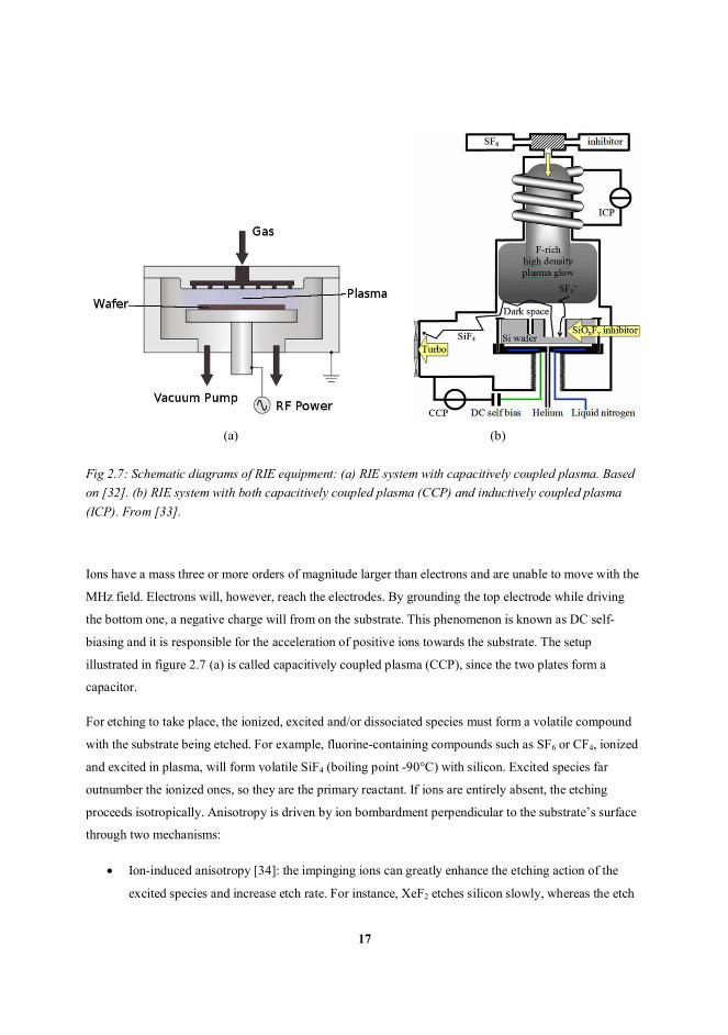
In the system illustrated in figure 2.7 (a), a reactant gas is introduced into the chamber through a
showerhead top electrode, and an RF field (typical frequency of 13.6 MHz) creates a gas discharge
plasma between the top and bottom electrodes.
17
(a) (b)
Fig 2.7: Schematic diagrams of RIE equipment: (a) RIE system with capacitively coupled plasma. Basedon [32]. (b) RIE system with both capacitively coupled plasma (CCP) and inductively coupled plasma(ICP). From [33].
Ions have a mass three or more orders of magnitude larger than electrons and are unable to move with the
MHz field. Electrons will, however, reach the electrodes. By grounding the top electrode while driving
the bottom one, a negative charge will from on the substrate. This phenomenon is known as DC self-
biasing and it is responsible for the acceleration of positive ions towards the substrate. The setup
illustrated in figure 2.7 (a) is called capacitively coupled plasma (CCP), since the two plates form a
capacitor.
For etching to take place, the ionized, excited and/or dissociated species must form a volatile compound
with the substrate being etched. For example, fluorine-containing compounds such as SF6 or CF4, ionized
and excited in plasma, will form volatile SiF4 (boiling point -90°C) with silicon. Excited species far
outnumber the ionized ones, so they are the primary reactant. If ions are entirely absent, the etching
proceeds isotropically. Anisotropy is driven by ion bombardment perpendicular to the substrate’s surface
through two mechanisms:
Ion-induced anisotropy [34]: the impinging ions can greatly enhance the etching action of the
excited species and increase etch rate. For instance, XeF2 etches silicon slowly, whereas the etch

18
rate can be increased by a factor of 10 or 100 when applying Ar+ ion bombardment [35]. This
means that bottoms will be etched up to two orders of magnitude faster than sidewalls of channels
or blind-holes.
Inhibition-driven anisotropy: the etchant species with an added inhibitor form a passivating layer
on the substrate, inhibiting further etching. Ion bombardment removes this passivation layer from
the bottom but it remains on sidewalls. This way, etching continues in the direction of the ion flux
and is inhibited at the sidewalls. An example is anisotropic etching of silicon with SF6 and O2; in
this system, silicon oxyfluoride [33] [34] is formed on the silicon surface, which inhibits further
etching at the sidewalls while it is removed from other surfaces by ion bombardment. Silicon
oxyfluoride is only stable at low (T< -100ºC) temperature, which necessitates a cryogenic cooling
unit to be integrated in the RIE tool.
Another approach is alternating the introduction of etching and passivating gases. In the first step
of the cycle, passivating gas is introduced (C4F8), which creates a layer of passivating
fluoropolymer on the silicon surface. In the next step, the etchant gas (SF6) is introduced in the
chamber, ion bombardment removes the passivation layer from the bottom of the trenches/blind
holes, and a small amount of silicon is etched isotropically. Subsequently the etchant gas is
evacuated and the passivating gas is re-introduced, forming a fresh passivation layer on the
exposed silicon surfaces, and the process is repeated. This method of etching is called pulsed (or
Bosch) process. Both cryogenic and Bosch RIE processes are termed deep RIE (DRIE), because
of the high aspect ratios and depth of etched structures that can be created.
The isotropically etched silicon structures visible in figure 2.6 (b) were obtained by minimizing the ion
energy, which minimizes ion-induced anisotropy: for this, the CCP power had to be reduced to ~3 W,
while the density of the plasma had to be high. These two goals are mutually exclusive in a simple CCP
device such as the one described in figure 2.7 (a). To achieve high density of plasma while separately
controlling the ion energy, a device with an inductively-coupled plasma (ICP) unit can be used (figure 2.7
(b)). Specifically, the features in figure 2.6 (b) were obtained with an Oxford Instruments Plasmalab
System 100, with an ICP power of 2 kW and pure SF6 gas at room temperature [31]. Unlike with the
device described in figure 2.7 (a), a system that contains both CCP and ICP such as the one in figure 2.7
(b) allows for the separate regulation of the concentration of ions and their acceleration towards the
substrate. Combined with a cryogenic cooling unit, such a device allows for very high aspect ratio
structures etched in silicon, because cryogenic temperatures enhance the passivating effect of silicon
oxyfluoride, while high-density plasma allows for high etch rates (as high as 7 μm/min).

19
It should be noted that isotropic etching with a CCP setup is obtained if the base pressure is kept
relatively high (~100 mTorr), to achieve frequent ion collisions and poor directionality.
The same Plasmalab System 100 apparatus was used to obtain the features in figure 2.8 (a), but with SF6
+ O2 (O2/SF6 flow rate ratio was 15 sccm : 100 sccm) gases at -110ºC [I]. In this instance, inhibition-
driven anisotropy is at play, where silicon oxyfluoride inhibits sidewall etching. The sidewalls display a
slight negative tapering. The negatively tapered profile appears in the case of high SF6 to O2 gas ratio (
[36], chapter 23), probably caused by ion bowing, i. e. the deflection of ions entering a trench or blind
hole as they are attracted to the negatively charged sidewalls [34] [37].
In figure 2.8 (b) we can see a SEM image of silicon nanograss (also known as “black silicon”), formed by
etching silicon in the same reactor as in figure 2.8 (a), but with much higher O2/SF6 flow ratio of 18 sccm
: 40 sccm [I] [II] [III]. Here silicon oxifluoride is generated at such high rate that ion bombardment is not
removing it from the bottom of the etched structures at a sufficient rate, and a quasi-regular array of
needle-like pillars is formed [34].
(a) (b)
Fig. 2.8: SEM images: (a) 50 μm deep channels etched in silicon using cryogenic RIE [IV], The profileexhibits negative taper due to ion bowing. (b) Silicon nanograss formed using cryogenic RIE in highlypassivating conditions [I].
It is established that the critical parameters in formation of silicon nanograss during SF6/O2 cryogenic RIE
of silicon are the O2 to SF6 flow rate proportion and the substrate bias [38]; silicon nanograss is more
likely to form when the oxygen fraction is high and the bias voltage (and hence the impinging ion energy)
is lower (figure 2.9 (a)). This is explained by the fact that the increased oxygen fraction increases the

20
production of silicon oxyfluoride, and an increased ion energy is necessary for its removal. Height, width,
slope and density of the silicon nanograss can all be controlled by changing the RIE process parameters, i.
e. O2 to SF6 flow rate proportion, chamber pressure, plate power, and substrate temperature [39]. Figure
2.9 (b) shows SEM images of four different silicon nanograss shapes, obtained by tuning the
abovementioned parameters.
(a) (b)
Fig. 2.9: Black silicon formation and morphology: (a) diagram of conditions for appearance of siliconnanograss (“columnar microsilicon – CMS”) depending on O2/SF6 flow rates and substrate bias. From[38]. (b) SEMs of various silicon nanograss morphologies. From [39].
Masks used for RIE etching of silicon in SF6 or SF6 + O2 gas range from ones that offer poor etch
selectivity, such as photoresists and silicon nitride (~10:1) through medium selectivity offered by silicon
oxide (~300:1) all the way to metallic aluminium and ALD alumina, which offer ~10000:1 etch
selectivity, especially with low ion energies (low CCP power). In general, DRIE equipment with an ICP
module allow for higher etch selectivity than simple CCP RIE equipment, because with ICP, the ion
bombardment of the substrate and hence the damaging of the mask can be kept low while the silicon etch
rate is high thanks to the high density of the plasma generated by ICP.
Examples of DRIE of silicon in micro fuel cell microfabrication are numerous [40] [41] [42] [43] [44]
[45] [46]. In this thesis DRIE was used to etch flowfield microchannels and through-wafer gas inlets [I]
[III]. DRIE of silicon allows for good control of channel depth and aspect ratio, vertical sidewalls and
arbitrary topology of fluidic channels – this level of flexibility is important when designing microfluidic
devices, including MFCs. Figure 2.10 shows an SEM of an electrode/current collector structure

21
microfabricated by DRIE. The structures would have been impossible to etch using isotropic or
anisotropic wet etching of silicon.
Fig. 2.10: SEM image of an electrode/current collector microfabricated by DRIE from a SOI wafer. Thefine grid at the bottom of the circular holes is etched from the device layer. From [45].
2.2.3 Anisotropic wet etching
When etching monocrystalline silicon with alkaline solutions, etch selectivity between various crystalline
planes exist [47]. Because of this, the etch rate is anisotropic and the cavity will have straight sidewalls
delimited by the slow-etching crystallographic planes. Figure 2.11 (a) shows the crystal structure of
silicon – known as diamond lattice – and the three main crystallographic planes, (100), (110) and (111).
The (100) etches much faster than the (111) plane. This difference is caused by the fact that, when etching
in the (100) direction, each silicon atom exposes two bonds towards the solution while the other two
bonds connect it to the lattice, whereas in the (111) direction, only one bond is exposed to the etchant
solution [47]. The atom attacked from the (111) direction is harder to remove, because an OH- group
attached to it will not significantly weaken the three bonds attached to the lattice, unlike with (100) atoms,
where two OH- groups attached to them will change the shape of the orbitals and weaken the other two
bonds, promoting removal and etching.

22
Fig. 2.11: (a) Schematic of diamond lattice, (b) (100) crystallographic plane, (c) (110) crystallographicplane and (d) (111) crystallographic plane. From [47].
A (100) silicon wafer is oriented so that one of the (100) planes is parallel to the surface of the wafer.
Figure 2.12 shows the result of etching such a wafer in an alkaline etchant, with two different rectangular
apertures in the etch mask. The etching proceeds until the (111) planes meet, or until the wafer has been
etched through.
Fig. 2.12: Anisotropically wet-etched silicon wafer, (a) top view and (b) cross section. From [48].
The most common alkaline silicon etchants are KOH and tetramethylammonium hydroxide (TMAH),
though NaOH, LiOH, organic amines etc. could also be used. Both KOH and TMAH have a high etch
rate of (100) and high-index planes. TMAH has a lower selectivity between (100) and (111) planes, and
the etched surfaces are more rough than those etched with KOH [49]. In spite of this, TMAH is often used
in a cleanroom environment, because the potassium present in KOH is incompatible with CMOS
fabrication processes.

23
Thermal silicon oxide, and silicon nitrides are practical and very efficient etch masks for KOH and
TMAH etching of silicon. Most photoresist are not suitable for this purpose, as they are attacked by
concentrated alkaline solutions, especially at temperatures higher than 20°C.
For microfluidic applications, alkaline etching of silicon has some drawbacks, as it imposes some
restrictions regarding channel aspect ratio (for (100) wafers)) and topology. However, the technology has
found some applications for micromachining of compartments with thin membranes for solid oxide fuel
cells (SOFC) [50] [51] and polymer electrolyte (PEM) MFCs [52] [46]. Figure 2.13 shows a typical
process for SOFC microfabrication by KOH etching of silicon. The silicon nitride deposition step is not
shown.
Fig. 2.13: Microfabrication of a SOFC by KOH etching of silicon: (a) Etching of silicon nitride with RIE.(b) KOH etching of silicon through wafer. (c) Deposition solid-oxide electrolyte. (d) Removal of siliconnitride by RIE etching from back side. Adapted from [50].
In principle, some form of silicon MFC described in [I] [II] [III] could be made using wet anisotropic
etching, but DRIE allows for much higher freedom in choosing width and depth of channels. Besides that,
long (~10 mm) channels with 50-100 μm spacing require very precise alignment of lithographic patterns
to the wafers’ crystallographic plane. Finally, since black silicon is created by DRIE, the process is
simplified by using the same tool for microfabricating also the channels and inlet holes.
2.3. Thin-film technologies
A very important part of microfabrication is the deposition of various thin films, be it metals, organic
materials or ceramics. These thin films perform a multitude of functions, such as etch masks, conducting
or semi-conducting layers, passivation/encapsulation, catalysis, bio-compatibility, electrical isolation etc.
24
The main thin-film technologies in microfabrication are
Evaporation
Sputtering
Plasma-enhanced chemical vapor deposition (PECVD)
Low-pressure chemical vapor deposition (LPCVD)
Atomic layer deposition (ALD)
Electroplating
Spin coating
This is not a definitive list of existing thin film deposition technologies; examples of notably missing ones
include pulsed laser deposition (PLD) and molecular beam epitaxy (MBE). Even though it is not a thin
film technology, screen printing should be mentioned, as it is often used in fuel cell and micro fuel cell
fabrication.
Two important properties of thin film deposition should be mentioned:
Conformality is the capability of a deposition process to cover hills, valleys, and undercuts. For instance,
evaporation has poor conformality, meaning that sidewall coverage is poor. In contrast, ALD is
characterized by excellent conformality, and even deep trenches can be covered.
Uniformity describes how even the deposited film thickness is across a wafer or sample. Evaporated films
can be very uniform even though they have poor conformality. ALD films have both good uniformity and
conformality.
2.3.1 Evaporation and sputtering
Evaporation and sputtering are technologies that belong to the more general class of physical vapor
deposition (PVD) [48], in which atoms are expelled from a target via heating, ion bombardment or laser

25
ablation, and transported to the substrate (usually in vacuum), where film forms because of metal vapor
condensation into a solid. PVD is the leading method for thin film metal and metal alloy deposition.
Conceptually, evaporation is a simple technique: it requires a vacuum chamber and a heated crucible
(figure 2.14 (a)) in which the material to be evaporated is placed. The crucible content is heated with a
heating element or electron beam. The chamber pressure is quite low (typically ~10-6 Torr, and as low as
10-11 Torr), so the atoms of the evaporated species do not collide, and therefore travel towards the
substrate with a line-of-sight directionality. This, in turn, produces a non-conformally deposited layer
with very little material deposited on vertical sidewalls.
Fig. 2.14: Schematic of an evaporator (a) and a sputter (b).
A sputtering apparatus uses accelerated argon ions (or some other suitable noble gas), which hit the target
– the metal or alloy to be sputtered – and eject atoms in kinetic collisions. These atoms travel to the
substrate where they transfer some of their energy to the substrate, cool down and solidify. The deposition
is more conformal than in the case of evaporation, as the sputtered atoms collide frequently before
reaching the substrate, due to the relatively much higher pressure in a sputtering chamber (1-10 mTorr).
Another difference compared to evaporation, is that sputtered atoms possess a much higher energy than
evaporated ones, and considerable heating of the substrate is possible. Furthermore, some weakly bound
particles may be re-sputtered from the substrate. Consequently, the deposited film is usually denser and
the adhesion is improved.

26
In a DC sputter (figure 2.14 (b)), electrons travel from the cathode to the anode, colliding with the argon
atoms and ionizing them. In the case of magnetron sputters, a magnetic field forces the electrons into a
circular path, greatly increasing the likelihood of collision with, and ionization of argon atoms. In case of
non-conductive target materials, RF sputtering is used, where the ionizing electrons move back and forth
between the electrodes.
Evaporation [40] or sputtering [42] [43] [53] [54] of gold is often used in MFC microfabrication, to
produce current collectors on top of non-conductive flowfields. Platinum sputtering [41] [53] or
evaporation [55] are methods used by some authors to produce a catalyst layer for MFCs.
In this thesis, chromium sputtering was used to deposit a thin film on silicon [I] [II] [III] [IV] and
aluminium [V] MFC chips, to protect the substrate from corrosion and formation of non-conductive
oxide. In MFC microfabrication it is common to deposit gold or platinum by PVD. Often these are thick
layers as the flowfield itself is poorly conductive. In [I], it was found that just chromium, usually an
adhesion layer for other metals, is itself suitable for metalizing the flowfield and the use of expensive
noble metals is unnecessary. Furthermore, the use of highly-conductive silicon allowed for a thin metallic
layer, instead of a thick one.
An interesting example of PVD of metals for MFC fabrication is the device described in [40] (figure
2.15): a 3 μm thick evaporated gold layer with 70 nm of titanium adhesion layer functions as a current
collector. Over the gold layer, 100 nm of molybdenium silicide (MoSi2) was sputtered. Finally, a very
thin (2.5 nm) layer of iron was evaporated on top of MoSi2, which acted as carbon nanotube (CNT)
growth catalyst. This design achieves high current and power densities, but the many deposited layers -
most notably 3 μm thick gold - make it expensive to fabricate.

27
Fig. 2.15: Diagram of MFC with several metallization layers. From [40].
2.3.2 Chemical vapor deposition (CVD)
Chemical vapor deposition (CVD) includes a chemical reaction in the process of deposition. Typically,
one or more reactant gases (precursors) are introduced in the reaction chamber, where the molecules are
activated via high temperature, plasma, or a combination of both. In plasma-enhanced CVD (PECVD),
part of the energy needed to activate the chemical reaction is provided by plasma enhancement –
production of activated radicals in the precursor gases - although the substrate itself may be heated to a
few hundred degrees °C. In the case of low-pressure CVD (LPCVD) activation energy for the chemical
reaction is thermal only and LPCVD operating temperatures are typically higher than with PECVD.
The precursor molecules adsorb onto the surface of the substrate (Figure 2.16) where the chemical
reaction (for instance, pyrolysis, hydrolysis, reduction etc.) takes place. As a consequence, a non-volatile
compound or element is deposited, while the volatile reaction products are desorbed.

28
Fig. 2.16: Illustration of film formation in chemical vapor deposition (CVD).
Low pressure CVD (LPCVD) reaction chambers are heated to high temperatures, e. g. 625ºC for
polysilicon deposition, 800ºC for silicon nitride deposition. A typical implementation of LPCVD reactor
is a quartz tube with heated walls, in which a cassette of wafers is inserted. LPCVD is characterized by
high purity, stoichiometric films conformally deposited on both sides of the wafer [7]. Unfortunately, the
high temperature required makes LPCVD unsuitable in circumstances where polymers or metals melting
at low temperatures, such as aluminium, are present.
In plasma-enhanced CVD (PECVD), the precursor gases are brought into higher activity state with the
use of plasma. As the plasma must be formed in the proximity of the substrate, PECVD devices usually
use reaction chambers where one or more wafers are placed face-up, and material is deposited on that side
only. The substrate itself must be heated, but the temperatures involved are lower than for LPCVD;
namely 300°C or less. The deposition rate is higher than or equal to LPCVD, but the films are often not
stoichiometric and are less dense than LPCVD films. For example LPCVD deposition of polysilicon in a
Centrotherm® furnace at 620ºC is 8-9 nm/min while with an Oxford Instruments PECVD reactor at
300ºC it is 10-15 nm/min.

29
2.3.3 Atomic layer deposition (ALD)
With atomic layer deposition (ALD), thin films are deposited one monolayer at a time. This is achieved
by cyclically pumping and evacuating two precursor gases in a sequence: the first precursor forms a
monolayer of a given species, then it is evacuated and the second precursor is introduced, which reacts
with the first monolayer in such way that a new monolayer can be formed on top of it. ALD films are
characterized by a very high level of uniformity. The downside of ALD is the slow growth rate, which is
less than 0.1 nm per cycle. Depending on the depth and aspect ratio of the structures to be coated, a cycle
can last from less than one second to over a minute [56].
2.3.4 Electroplating
Electroplating is an electrochemical technique used to deposit relatively thick layers of metal on
conductive layers (or non-conductive substrates such as glass or polymers with a conductive seed layer).
Since in micro fuel cells the reduction of ohmic losses is imperative, electroplating is often used in their
microfabrication. Thick resists are often used with electroplating (figure 2.17) to obtain ridge or columnar
structures. By overplating, mushroom-like structures (figure 2.17 (d)) or even capped structures (figure
2.17 (e)) are possible [57].
Fig. 2.17: Electroplating process: (a) seed layer deposition and patterning of thick resist, (b)electroplating, (c) stripping of resist. (d) overplated features are obtained if plating continues beyond (b).(e) stripping of resist, (f) continuing the over-plating can produce capped channels.

30
In [58], the entire flowfield was microfabricated from electroplated copper. The substrate itself was a
copper film.
A catalyst layer with large effective active area can be deposited by electroplating platinum [43] [59]
(often referred to as “platinum black”).
2.4. Laser ablation
Ablative techniques for material removal are very important in MEMS. Unlike etching, however, ablative
techniques like focused ion beam milling and laser ablation, do not need an etch mask; the energetic beam
is scanned across the ablated substrate according to a programmed pattern.
Figure 2.18 is a schematic of a laser ablation system, consisting of a pulsed laser source, a galvanometric
scanner which steers the laser beam in the XY axes, an XYZθ stage which moves the sample in all three
axes and also rotates it, and a controlling computer. In practice, the use of a galvanometric scanner makes
an XYZ stage often redundant. XYZ stages sometimes may have the option of rotating the sample, but it
adds substantially to the cost of the system. The controlling computer may control all these parts. It
should be noted that a galvanometric scanner allows for much faster beam scanning but have lesser
positional accuracy compared to an XYZ stage. Furthermore, using an XYZ stage may be mandatory
when ablating large samples.

31
Fig. 2.18: Schematic of a laser ablation system. The computer in the bottom right controls the XYZθstage, the galvanometric scanner and the laser source.
Laser ablation can be performed using two modes: continuous wave (CW) and pulsed ablation. Pulsed
ablation allows for better control of energy deposited in the substrate, by adjusting the pulse duration and
the frequency of the pulses. By using very short pulses of high intensity light, it is possible to minimize
the heat affected zone (HAZ) around the ablated region, while substantially increasing the beam intensity
[60] [61] compared to CW.
Laser ablation is potentially a very flexible microfabrication method, as it allows for the micromachining
of almost every solid material: metals [62] [63] [64], ceramics [63] [65] [64], polymers [63] [66], glass
[67] [65], fused silica [65], silicon [68] [62], and diamond [62]. In this thesis, laser ablation has been used
to fabricate flow channels and inlets in silicon MFCs [IV].

32
(a) (b)
(c) (d)
Fig. 2.19: Examples of laser-ablated materials. (a) steel [63], (b) polyimide [63], (c) diamond [62] and(d) silicon [62].
Some of the main parameters of a pulsed laser system are the pulse duration, the repetition rate (in Hz),
fluence (energy per unit area of one pulse), peak power of the pulse and sustained power. Solid-state
lasers produce a beam with a Gaussian profile. The diameter or radius of such beam is determined either
by the point at which the intensity falls to 1/e2 of the central peak (figure 2.20), or as full width half
maximum (FWHM), in which case the point is the one at which the intensity falls to ½ of that of the peak.
Lasers with gaseous medium, such as excimer or copper vapor lasers (also used for laser ablation) do not
typically produce beams with a Gaussian profile but a non-Gaussian rectangular or circular profile.

33
Fig. 2.20: Gaussian profile of beam intensity and its 1/e2 diameter.
The physical phenomena behind laser ablation are diverse, and depend on pulse duration, beam
wavelength and peak intensity. These phenomena include multiphoton, avalanche [69] and tunnel
ionization [67], explosive melting and evaporation [68] [70], sub-picosecond disordering of the crystal
lattice [71] [72], Coulomb explosion [73], and inverse bremsstrahlung producing deep-penetrating X-rays
[74]. The nature of these phenomena is crucial, because they determine, among other things, how well the
ablated material absorbs the laser beam photons. To minimize the heat-affected zone (HAZ), induced
stresses, burrs (spallation around the ablated feature), average size of ejected droplets, as well as the total
thermal energy deposited in the substrate, one should maximize photon absorption in the ablated material.
The better the photon absorption in the ablated material, the more of the energy goes into material
ablation instead of heating the substrate.
With nanosecond-range pulse durations, the main ablative phenomenon seems to be melting and
explosive ejection of molten material [68] [70]. Decreasing the beam wavelength is a very effective
method to achieve higher light absorption and better ablation quality [65] [68]. The importance of
wavelength for nanosecond ablation quality is illustrated on figure 2.21, which shows a dramatic
improvement of feature quality and decrease of amount of ablated glass, by decreasing the wavelength
from 193 nm to 157 nm. Alternatively, doping the substrate material to achieve higher light absorption is
a possibility that can sometimes be utilized [65] [75].

34
(a) (b)
Fig. 2.21: Germanium-doped fused silica on silicon ablated with excimer lasers: (a) single pulse withfluence F=3.6 J cm-2, wavelength λ=193 nm, removed the entire layer (28 μm) of fused silica. (b) 100pulses, F=3.0 J cm-2, λ=157 nm, removed 6 μm of fused silica. From [65].
Large bandgap materials such as quartz, alumina and PTFE, are challenging to ablate with nanosecond
pulses. Even with short wavelength excimer lasers, nanosecond ablation relies on single-photon ionization
of defect states, two-photon ionization at high fluences or formation of defects during the long pulse [65].
An empirical formula for threshold fluence (minimum fluence at which ablation is observed) exists [76]
[77]: 𝐹 ∝ √τP (1.1)
where τP is the pulse duration. This formula is valid for pulse duration down to about 10 ps, below which
the trend changes, indicating that the nature of the breakdown process is different than with shorter
pulses. Indeed the thermal nature of nanosecond pulse ablation is controlled by thermal conduction
through the lattice [77] [78], and as pulse duration decreases below 10 ps, thermal conduction becomes
less significant and there is both a qualitative departure from (1.1), as well as a qualitative change in the
ablated zone, which becomes more localized.
In case of ultrashort pulses (τP < 150 fs) electron ionization leads to covalent bond breaking and lattice
disorder, in a timeframe that is too short for the excited state electrons to couple with the lattice phonons
[71] [72] [67]. Therefore, when ablating with ultrashort laser pulses, the heating of the substrate is very
small. This ablation regime does not rely on melting and explosive ejection of droplets; the expelled
material particles are in the nanometer scale, minimizing burr.
35
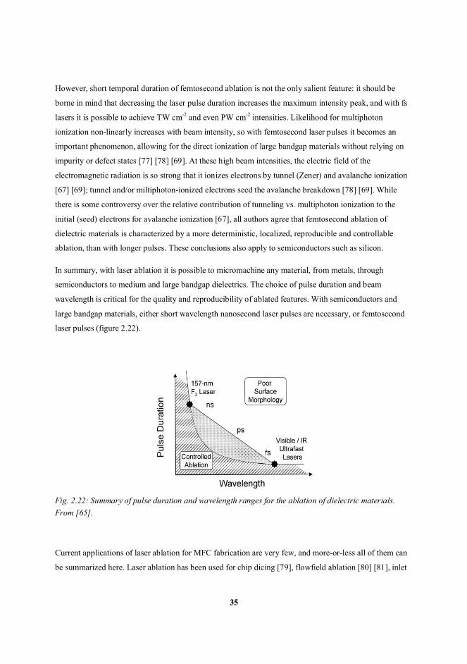
However, short temporal duration of femtosecond ablation is not the only salient feature: it should be
borne in mind that decreasing the laser pulse duration increases the maximum intensity peak, and with fs
lasers it is possible to achieve TW cm-2 and even PW cm-2 intensities. Likelihood for multiphoton
ionization non-linearly increases with beam intensity, so with femtosecond laser pulses it becomes an
important phenomenon, allowing for the direct ionization of large bandgap materials without relying on
impurity or defect states [77] [78] [69]. At these high beam intensities, the electric field of the
electromagnetic radiation is so strong that it ionizes electrons by tunnel (Zener) and avalanche ionization
[67] [69]; tunnel and/or miltiphoton-ionized electrons seed the avalanche breakdown [78] [69]. While
there is some controversy over the relative contribution of tunneling vs. multiphoton ionization to the
initial (seed) electrons for avalanche ionization [67], all authors agree that femtosecond ablation of
dielectric materials is characterized by a more deterministic, localized, reproducible and controllable
ablation, than with longer pulses. These conclusions also apply to semiconductors such as silicon.
In summary, with laser ablation it is possible to micromachine any material, from metals, through
semiconductors to medium and large bandgap dielectrics. The choice of pulse duration and beam
wavelength is critical for the quality and reproducibility of ablated features. With semiconductors and
large bandgap materials, either short wavelength nanosecond laser pulses are necessary, or femtosecond
laser pulses (figure 2.22).
Fig. 2.22: Summary of pulse duration and wavelength ranges for the ablation of dielectric materials.From [65].
Current applications of laser ablation for MFC fabrication are very few, and more-or-less all of them can
be summarized here. Laser ablation has been used for chip dicing [79], flowfield ablation [80] [81], inlet

36
hole ablation [10] [82] [83], direct patterning (without lithography step) of etch mask [84] and electrolyte
membrane segmentation [85]. In this thesis, both inlet holes and flowfield channels have been obtained by
laser ablation [IV]. In many of these applications, sidewall quality (uniformity, lack of burr, precisely
controlled depth or width etc.) are of minor importance, and the laser parameters could be chosen to
maximize speed of ablation. Laser ablation has been used to simplify the microfabrication process by
avoiding one or more lithography steps, and it allows for fast prototyping of fuel cell topologies and
geometries.
2.5 Other technologies for micro fuel cells
The microfabrication processes used for the creation of the micro fuel cells described in this thesis require
some additional techniques in addition to the ones listed in the previous subsections:
Drilling: all the fuel cells studied in the author’s works use inlet holes through which gases are
brought to the flowfields. In the case of aluminium micro fuel cells, these inlet holes had to be
drilled, either using CNC equipment, or manually [V]. Brittle silicon and glass wafers are not
amenable to drilling, and inlet holes are made by etching [I] [II] [III], laser ablation [IV] or sand
blasting [41].
Dicing: usually wafers accommodate more than one device – typically, many more. To separate
these devices, the wafer has to be cut apart into chips. This is typically done with a precision-
controlled dicing saw with rotating diamond blade. The feed rate (relative speed of the rotating
blade and the wafer) and the blade rotation speed, have to be chosen depending on the material or
materials being diced. Silicon is usually diced with thin (50 μm) blades made of diamond in a
resin binder. For aluminium wafers, a thicker (200 μm) blade from diamond in a nickel binder is
more suitable, and the feed rate is much lower than with silicon wafers.

37
Oxidation: thermally-formed silicon oxide has the best quality, uniformity, stoichiometry, and
purity of all competing methods for the formation of silicon oxides. It is a good choice for
masking with KOH etching and RIE etching of silicon [I] [III]. To thermally oxidize a silicon
wafer, it has to be placed in an oven at ~1000°C in an oxygen-containing atmosphere [7]. It is
very convenient when more than just a few wafers have to be processed, because a typical
oxidation furnace can oxidize several dozen wafers at once.
Catalyst deposition on Nafion® membranes: while there have been efforts to deposit platinum
and other noble metal catalysts onto Nafion® membranes (the electrolyte of choice for low
temperature fuel cells) by sputtering [86], a more commonly used method to producing
membrane-electrolyte assemblies (MEA) is to spray-coat the membrane with carbon black
powder on which platinum nanoparticles have been deposited [87]. This is the method used in [I].
The carbon black-containing paint is prepared using Wilson and Gottesfeld’s method [88]. An
alternative to spray-painting the membrane is to add (e. g. by brushing or spraying) the catalyst-
loaded carbon black onto carbon paper which is then hot-pressed onto a Nafion® membrane [89].
Bonding: MEMS components have to be usually protected from their environment in such way
that their function is not affected. For instance, MEMS resonators need a stable ambient gas, or
vacuum, for their functioning, and microfluidic reactors must protect the vessels and reactor
chambers from contamination and loss of fluid [12]. For this purpose, the wafer with MEMS
components can be bonded to a capping wafer. Bonding can also be used to achieve more
complex devices, i. e. increase the devices’ 3D complexity.
This method is commonly used for microfluidic devices in general, but rarely for MFCs.
Examples of microreactors for use in a MFC system however do exist [90] [91].
In MFC fabrication adhesive bonding is more common. For instance, in [43], a polyimide layer
was used to adhesively bond a silicon substrate to a Nafion® membrane, and in [87], a MFC
stack was realized by bonding polymethyl-methacrylate (PMMA) plates and silicone gaskets
using acrylic adhesive.

38
Carbon nanotube (CNT) deposition: carbon nanotubes are micrometer-long tubular structures
with a diameter of ~1 nm. CNTs are an effective and popular choice for catalyst support, and are
often used for catalyst support in fuel cells [92]. CVD is the most common method of CNT
production [93]. The CNTs used in fuel cells are typically treated as a bulk material, and are
applied to Nafion® or other electrolytic membrane by spray-painting, brushing or other such
manufacturing technology. Kuriyama et al. have, however, deposited CNTs directly on a
conductive substrate to form a gas diffusion layer and catalyst support, by CVD [40].

39
3. Fuel cells
This section describes fuel cells design and operation, and gives a panorama of the current research and
technologies in the field.
3.1. Fuel cell operation
Fuel cells produce electric energy from a fuel and an oxidizing agent in an electrochemical process (figure
1.3). In a fuel cell fed with hydrogen and oxygen gas, the reactions at the anode and cathode are
Anode: 2H2 → 4H+ + 4e- (3.1)
Cathode: O2 + 4e- + 4H+ → 2H2O (3.2)
Oxidation happens at the anode, where hydrogen molecules reach the catalyst sites and lose two electrons
per molecule. The H+ nuclei (protons) drift through the electrolyte, while the electrons travel through the
outside circuit, where they perform work. At the cathode, electrons close the circuit, O2 is reduced
forming water with protons. The electrolyte, in this case, is acidic, because in such a medium H+ ions are
mobile.
For these reactions to happen at low temperatures – even room temperature – catalysts are required. The
catalyst lowers the energy threshold for the reaction kinetics, effectively lowering the necessary
temperature at which the oxidation and reduction reactions occur. If present, these catalyst layers are
considered the actual electrodes of the fuel cell, and the unit composed of the electrolyte and the catalyst
layers is called a membrane-electrode assembly (MEA). Platinum is a typical catalyst for hydrogen-fueled
fuel cells, but others exist: platinum-ruthenium alloy, platinum-palladium alloy, nickel, and cobalt, for
example.
A more detailed diagram of a fuel cell on figure 3.1 shows the components found in most fuel cells. Gases
(or liquids) are brought to and from the fuel cell through a system of channels called flowfield. The
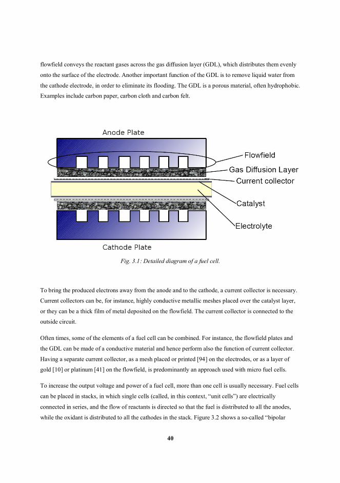
40
flowfield conveys the reactant gases across the gas diffusion layer (GDL), which distributes them evenly
onto the surface of the electrode. Another important function of the GDL is to remove liquid water from
the cathode electrode, in order to eliminate its flooding. The GDL is a porous material, often hydrophobic.
Examples include carbon paper, carbon cloth and carbon felt.
Fig. 3.1: Detailed diagram of a fuel cell.
To bring the produced electrons away from the anode and to the cathode, a current collector is necessary.
Current collectors can be, for instance, highly conductive metallic meshes placed over the catalyst layer,
or they can be a thick film of metal deposited on the flowfield. The current collector is connected to the
outside circuit.
Often times, some of the elements of a fuel cell can be combined. For instance, the flowfield plates and
the GDL can be made of a conductive material and hence perform also the function of current collector.
Having a separate current collector, as a mesh placed or printed [94] on the electrodes, or as a layer of
gold [10] or platinum [41] on the flowfield, is predominantly an approach used with micro fuel cells.
To increase the output voltage and power of a fuel cell, more than one cell is usually necessary. Fuel cells
can be placed in stacks, in which single cells (called, in this context, “unit cells”) are electrically
connected in series, and the flow of reactants is directed so that the fuel is distributed to all the anodes,
while the oxidant is distributed to all the cathodes in the stack. Figure 3.2 shows a so-called “bipolar

41
plate” stack. In this configuration, the flowfields act as current collectors – they are made of a conductive
material, such as graphite or steel. Variations of this configuration are very common with (macro) fuel
cells.
Fig. 3.2: Illustration of a fuel cell stack. (a) exploded view of a unit cell. (b) a bipolar plate stack.
In order for a fuel cell stack to be a useful device, it has to be integrated into a fuel cell system, which
includes functions such as reactant conditioning (e. g. filtration and humidification of air), thermal
stabilization (heating or cooling), pumping of reactants, output current conditioning, containers/reservoirs
of fuel and/or oxidant, water recycling etc. Many of the fuel cell types are most efficient with hydrogen as
fuel, but hydrogen is harder to store and is less available than natural gas, methanol or other
hydrocarbons. For this reason, often a fuel cell (including micro fuel cell) system includes a reformer,
which reforms methane, natural gas, methanol etc. into hydrogen [95] [9] [96] [42].
3.2. Fuel cell taxonomy
To become familiar with the vast world of fuel cells, classifications are useful. Fuel cells are usually
classified based on their electrolyte. The choice of electrolyte in the fuel cell determines the temperature
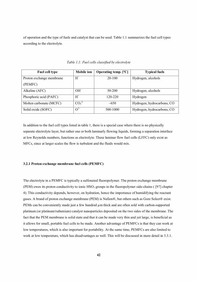
42
of operation and the type of fuels and catalyst that can be used. Table 1.1 summarizes the fuel cell types
according to the electrolyte.
Table 1.1: Fuel cells classified by electrolyte
Fuel cell type Mobile ion Operating temp. [ºC] Typical fuels
Proton exchange membrane
(PEMFC)
H+ 20-100 Hydrogen, alcohols
Alkaline (AFC) OH- 50-200 Hydrogen, alcohols
Phosphoric acid (PAFC) H+ 120-220 Hydrogen
Molten carbonate (MCFC) CO32- ~650 Hydrogen, hydrocarbons, CO
Solid oxide (SOFC) O2- 500-1000 Hydrogen, hydrocarbons, CO
In addition to the fuel cell types listed in table 1, there is a special case where there is no physically
separate electrolyte layer, but rather one or both laminarly flowing liquids, forming a separation interface
at low Reynolds numbers, functions as electrolyte. These laminar flow fuel cells (LFFC) only exist as
MFCs, since at larger scales the flow is turbulent and the fluids would mix.
3.2.1 Proton exchange membrane fuel cells (PEMFC)
The electrolyte in a PEMFC is typically a sulfonated fluoropolymer. The proton exchange membrane
(PEM) owes its proton conductivity to ionic HSO3 groups in the fluoropolymer side-chains ( [97] chapter
4). This conductivity depends, however, on hydration, hence the importance of humidifying the reactant
gases. A brand of proton exchange membrane (PEM) is Nafion®, but others such as Gore Select® exist.
PEMs can be conveniently made just a few hundred μm thick and are often sold with carbon-supported
platinum (or platinum/ruthenium) catalyst nanoparticles deposited on the two sides of the membrane. The
fact that the PEM membrane is solid state and that it can be made very thin and yet large, is beneficial as
it allows for small, portable fuel cells to be made. Another advantage of PEMFCs is that they can work at
low temperatures, which is also important for portability. At the same time, PEMFCs are also limited to
work at low temperature, which has disadvantages as well. This will be discussed in more detail in 3.3.1.

43
PEMFCs with platinum as catalyst are commonly used for hydrogen fuel cells [41] [98] [99]. The
electrode reactions for a PEMFC when fueled with hydrogen were mentioned previously; (3.1) for the
anode and (3.2) for the cathode. Such fuel cells are a popular choice for MFCs, in spite of the challenges
associated with hydrogen storage [100]. One approach to solve the storage issue is by reforming an easily
storable fuel such as methanol, to produce hydrogen [95] [9]. If a thermal reformer is used, the resulting
hydrogen gas will contain carbon monoxide, which poisons the catalyst platinum sites in the anode. The
poisoning problem is solved by using a platinum-ruthenium (PtRu) alloy as catalyst for the anode [101].
Another solution to the presence of CO in the reformed gas is using a hydrogen-selective permeable
membrane in the reformer itself, thus yielding pure hydrogen [96].
Another approach is using methanol or other alcohols as a fuel, directly (without reformation into
hydrogen) [102] [103] [104]. Such fuel cells are called direct methanol (DMFC) or direct alcohol fuel
cells (DAFC).
The anode and cathode reactions in a PEM DMFC ( [97] chapter 6) are
Anode: CH3OH + H2O→ 6H+ + 6e- + CO2 (3.3)
Cathode: 3/2 O2 + 6e- + 6H+ → 3 H2O (3.4)
An intermediary product in the anodic reaction is carbon monoxide. As mentioned before, this can poison
the platinum catalyst, so for direct methanol PEMFCs, PtRu is the preferred anodic catalyst.
A typical approach for the realization of PEM MFCs is to utilize commercial PEMs while
microfabricating the flowfields and current collectors. Indeed, all the MFCs that are part of this thesis
have been implemented in this way.
One interesting example of a PEM MFC is the micro-and-nanofabricated microbial fuel cell demonstrated
in [105]. In this cell, a carbon nanotube (CNT) forest is grown on the bottom of a basin microfabricated in
silicon (figure 3.2.1). The CNT forest increases the contact area with the anodic reactant and also to
promote microbial adhesion and colonization. This cell generates a few μA and several hundred nW
(nanowatts), which is a relatively good result for a microbial fuel cell. The fuel introduced in the anodic
chamber was either wastewater or an acetate nutrient. The nickel silicide area functions simply as a low-
resistance contact pad.

44
Fig. 3.2.1: Microbial PEM MFC. (a) Construction. (b) SEM micrograph of anode basin with carbonnanotube forest From [105].
In another implementation of a PEM micro fuel cell, Wang et al. [106] constructed the current collector
plates from pyrolysed, mechanically machined polyimide (Cirlex®) plates. During pyrolysis the current
collector plates shrink in volume, and an initial flowfield of 100 mm2 active area shrinks to 64 mm2
(figure 3.2.2). With this approach, the authors achieved a power density of 85 mW cm-2, with hydrogen as
fuel and oxygen as oxidant.
Fig. 3.2.2: Photograph of Cirlex® current collector plates (a) after and (b) before pyrolysis. From [106].

45
Finally, a third example of MFC with a PEM is given in [107]. In this instance, a PEM MFC lacking a gas
flowfield (figure 3.2.3 (a) and (b)) is wrapped around a cylindrical container (c) in which metal hydride
pellets are placed, forming an air-breathing MFC system with fuel storage. The pellets produce hydrogen
gas in presence of humidity. Humidity in the form of water vapor is recovered during cell operation by
diffusion from the cathode side facing outwards, towards the inner side facing the hydride pellets. The
hydrogen gas flow is regulated using a simple valve (not shown).
Fig. 3.2.3 PEM MFC system from [107]. (a) Cross section schematic of MFC. (b) Components of the cell.(c) Cylindrical container with MFC wrapped around.
A special case of PEMFC are porous silicon micro fuel cells: in [44] porous silicon is loaded with 8M
aqueous solution of sulfuric acid, resulting in a membrane that is effectively proton-conducting and
showing promising performance in a formic acid-fueled MFC. A more sophisticated approach to making
porous silicon proton-conductive is described in [108]: nanoporous (pore diameter 5-7 nm) silicon is
treated with 3-mercaptopropyltrimethoxysilane, to form an –SH group terminated monolayer (figure 3.3).
The –SH group is oxidized to –SO3H. The porous silicon is then capped with a thin layer of silica with
even narrower pores (1 nm) which keep water trapped inside, creating stable ambient for proton
conductivity of the –SO3H group.

46
Fig. 3.3: Nanoporous silicon membrane with proton-conducting monolayer. The capping (in dark grey) issilica with 1 nm diameter holes, keeping water(light blue) trapped. From [108].
3.2.2 Alkaline (AFC) and alkaline membrane fuel cells (AMFC)
Alkaline membrane fuel cells (AMFC) ( [109] chapter 2) are a sub-group of alkaline fuel cells (AFC),
with the difference that the aqueous sodium or potassium hydroxide solution in AFCs is replaced by a
solid-state membrane. AMFCs can be used in similar scenarios as PEMFCs: they use an anion-conductive
membrane as an electrolyte, which work at similarly low temperatures such as PEMFCs. AMCFs are
more tolerant to CO2 compared to AFCs: CO2 forms carbonates and bicarbonates, with sodium and
potassium, which precipitate in the electrolyte-filled pores [110].
In a hydrogen-fueled setup, the electrode reactions in AFCs are
Anode: 2 H2 +4 OH- → 4 H2O + 4e- (3.5)
Cathode: O2 + 2 H2O + 4e- → 4 OH- (3.6)
These reactions have improved kinetics compared to the ones in acidic media, which makes it possible to
use non-noble metals, such as iron, cobalt [111], silver and nickel [112] as catalysts. Another advantage
of AFCs and AMFCs is that the anodic catalyst can be CO-tolerant, and hence reformed gas can be used
directly as a fuel.
In spite of the advantages of alkaline membranes and the fact that they can, physically, be used much the
same way as PEM, no alkaline membrane-based MFCs were found in literature at the time of the writing

47
of this thesis. There are, however, examples of MFCs based on liquid alkaline electrolyte, either as single-
compartment MFCs [113], or flowing liquid MFCs [114] (figure 3.4). The design in [114] allows for the
use of a reference electrode inside the electrolyte.
Fig. 3.4: Diagram of a liquid alkaline MFC. From [114].
3.2.3 Phosphoric acid fuel cells (PAFC)
PAFC are the clear market leader in terms of units built and installed capacity, and they were the first fuel
cell technology to be commercialized ( [115] section 5). While both PAFCs and PEMFCs use a proton-
conducting electrolyte, in the case of PAFCs the electrolyte is a liquid: molten phosphoric acid. The
lowest temperature of operation, when using 100% concentrated phosphoric acid, is dictated by the
melting point of H3PO4, 42ºC ( [97], subsection 7.3). As with PEMFCs, the electrode equations for
hydrogen or methanol fuels are the same as previously noted (equations (3.1), (3.2) for hydrogen, and
(3.3), (3.4) for methanol), and the catalyst is identical as well – platinum or platinum alloys. Unlike
PEMFCs however, PAFCs can operate at higher temperatures (T > 160ºC) which makes them more

48
tolerant to CO poisoning of anode catalyst ( [115] subsection 5.2.4). Furthermore, humidification is not
necessary to maintain good proton conductivity [42] [116].
In [42] a MFC system consisting of a microreactor (for reformed hydrogen fuel production) and micro
PEFC is described. The membrane used was phosphoric-acid-doped polybenzimidazole (PBI). No
degradation of the membrane, operating at 180°C, was detected when the anodic feed contained as much
as 2% molar content of CO.
3.2.4 Molten carbonate fuel cells (MCFC)
MCFCs operate at 650°C and higher temperatures, and as the name implies, they use a mixture of molten
carbonates, lithium, sodium or potassium, as electrolyte. Thanks to the high temperature, these devices do
not need noble metal catalysts for efficient operation ( [115] section 6, [117]). The electrode reactions are
Anode: H2 +CO32- → CO2 + H2O + 2 e- (3.7)
Cathode: 1/2 O2 + CO2 + 2e- → CO32- (3.8)
The carbonate anion CO32- is the one transported through the electrolyte, effectively transferring CO2
from the cathode to the anode. For this reason, a MCFC system requires a means to provide CO2 to the
cathode gas stream. MCFCs are tolerant to CO contamination in the fuel gas [118].
The catalyst in MCFCs is nickel for the anode and NiO for the cathode. The electrolyte impregnates
porous lithium aluminate to form an electrolyte membrane. Calcium or barium carbonates are added to
the electrolyte to reduce its corrosion of NiO, [117].
The challenges in managing the high temperatures required for the operation of the MCFC, and the liquid
electrolyte-impregnated ceramic membrane, besides the CO2 circulation, are probable reasons for the
current lack of research in microfabricated MCFC. A micro-scale MCFC system would require
exceptional thermal isolation of the fuel cell from outside ambient, and should have a CO2 circulation
system. This is in addition to the fact that MCFCs cannot readily be started up or shut down, as would be
the common usage scenario of a MFC in use for portable applications.

49
3.2.5 Solid oxide fuel cell (SOFC)
SOFCs use a non-porous solid metal oxide electrolyte, operating at temperatures as high as 1000°C (
[115] section 7, [118]) such as yttria (Y2O3)-stabilized zirconia (ZrO2) YSZ, or cerium-gadolinium oxide
(CGD) [119]. Similarly to MCFCs, SOFCs do not need precious metals as catalyst, nor are they affected
by CO in the fuel feed. The electrode reactions are
Anode: 2 H2 + 2 O2- → 2H2O + 4 e- (3.9)
Cathode: O2 + 4 e- → 2 O2- (3.10)
The anodic catalyst is usually a cermet – a mixture of nickel metal with a ceramic such as YSZ. The
cathode is usually made from a perovskite, e.g. (La, Sr)MnO3 (LSM).
The O2- conductivity of the oxide electrolyte is strongly dependent on temperature, so to increase
conductance either the temperature should be increased or the electrolyte thickness should be decreased
[118].
Unlike MCFCs, there are many SOFCs implemented as MFCs [119] [120] [121] [51] [50]. For a micro
SOFC to be viable, it should have fast start-up and operate at lower temperatures than stationary SOFCs.
At the lower temperatures of micro SOFCs, the electrolyte is less conductive, so it is necessary to
microfabricate very thin membranes (as thin as 50 nm are reported) [119] [122]. To increase catalytic
activity at the anode at lower temperatures, noble metals may be added [123] [124].
A good design candidate for micro SOFC are single-chamber (SC) SOFCs, where a mixture of fuel and
oxidant are supplied to both electrodes, and correct operation relies on catalyst selectivity. Typically, SC-
SOFCs are fueled with a higher hydrocarbon (ethane, propane, ethanol, etc.) and oxidative reforming at
the anode produces CO and H2. The oxidative reforming is exothermic, maintaining the temperature of
the cell at 350°C-650°C, which is necessary for its electrochemical operation. SC-SOFCs offer several
advantages compared to conventional, dual-chamber cells: fast start-up through self-heating, structural
simplicity, simpler gas manifolding, and tolerance for cracks in the electrolyte [123]. All these properties
make SC-SOFCs suitable for portable applications and miniaturization. An example implementation of a
microfabricated SC-SOFC is pictured on figure 3.5 [121]: the anode is coated with a Ru + CeO2 cermet to
facilitate the reforming reaction.

50
Fig. 3.5: Schematic of a micro SC-SOFC. From [121].
3.2.6 Laminar flow fuel cell (LFFC)
When studying the flow of fluids in vessels, the dimensionless Reynolds number (Re) is defined as𝑅𝑒 = ∙ ∙μ
(3.11)
where D is the hydraulic diameter of the vessel, ρ is the density of the fluid, v is the mean velocity of the
fluid, and μ is the dynamic viscosity. The Reynolds number is a useful value because it gives an idea of
how turbulent the flow is. In microfluidic devices, when the fluid is a liquid, both v and D are small, and
according to (3.11), the Reynolds number will be small as well, typically Re < 10; in these circumstances,
flow will be laminar and it is possible to coalesce two separate streams without mixing. This allows for a
completely new class of fuel cells: laminar flow, or membraneless micro fuel cells [125]. Examples of
laminar flow MFCs are abundant [126] [127] [128] [129] [89]. In these devices, the fuel and the oxidant
are both dissolved in the electrolyte, which may be either acidic (proton-conducting) or alkaline (anion-

51
conducting). Laminar-flow devices completely solve the water management issues of low-temperature
fuel cells, and there is no membrane degradation.
Figure 3.6 shows two implementations of laminar flow fuel cells: (a) shows an optical micrograph of
laminar flow in the device from [126], while in (b) is a schematic of the construction of the MFC. The
device presented in [126] is the forerunner of laminar flow MFCs: the fuel was an aqueous solution of
formic acid, while the oxidant was a solution of potassium permanganate or oxygen dissolved in 0.5 M
sulfuric acid.
Fig. 3.6: (a) Micrograph of laminar flow of aqueous solutions. (b) schematic of symmetric laminar flowMFC, from [126]. (c) schematic of air-breathing laminar flow MFC, from [128].
In figure 3.6 (c) we see a schematic of the device presented in [128]. This device uses either an alkaline or
acidic electrolyte, and a number of fuels (formic acid, methanol, ethanol, hydrazine and sodium

52
borohydride). The most remarkable feature of this design is the porous cathode, through which oxygen
diffuses into the electrolyte, making it air-breathing.
3.3 Fuel cell characterization
This section gives an overview of the experimental techniques used to characterize fuel cells as a system.
Half-cell, catalyst and electrode characterization are outside the scope of the thesis and are not discussed.
The data most commonly gathered in fuel cell measurements include:
Open circuit voltage (OCV)
Polarization curves (or current-voltage curves)
Cyclic voltammetry (CV)
Chronoamperometric measurements (CA)
Electrochemical impedance spectroscopy (EIS)
All the above characterization data is obtained by connecting the fuel cell electrodes to a computer-
controlled potentiostat, which sets the voltage (or the current) at a pre-programmed value, while
measuring the current (or voltage) through the fuel cell. Figure 3.7 shows a schematic representation of a
MFC characterization setup, with an inset picture of a MFC measurement jig. This setup was used in this
thesis for all MFC performance characterizations. The jig is composed of two aluminium blocks directly
contacting the current collectors of the characterized fuel cell. This simple arrangement for the electrical
contact is possible due to the fact that the MFCs in this thesis are all made of conductive materials —
highly-doped silicon or bulk aluminium. The computer-controlled potentiostat is represented as an
electrical source with an output impedance. When the potentiostat controls the voltage while measuring
the current, the output impedance is very small. When the potentiostat controls the current flowing
through the fuel cell, the output impedance is infinite.

53
Fig. 3.7: measurement jig and schematic of computer-controlled potentiostat.
3.3.1 Open circuit voltage and polarization curves
The open circuit voltage (OCV) is obtained when fuel and oxidant are circulated through the fuel cell, but
no current flows through the outside circuit (i.e. the circuit is “open”). It can be shown ( [97], section 2)
that the voltage (or electro-motive force) of an ideal hydrogen-fueled fuel cell is𝐸 = ∆ (3.12)
where Δgf is the Gibbs free energy of formation of one mole of H2O, and F is the electric charge of one
mole of electrons. For a hydrogen-fueled cell at standard conditions (T=25°C, P=100 kPa), E = 1.2 V.
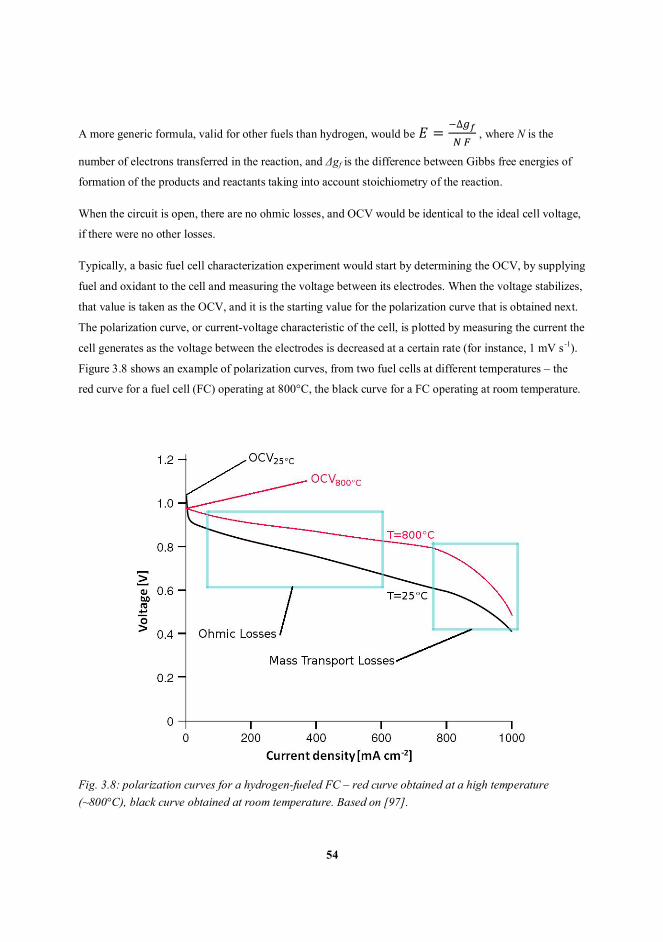
54
A more generic formula, valid for other fuels than hydrogen, would be 𝐸 = ∆ , where N is the
number of electrons transferred in the reaction, and Δgf is the difference between Gibbs free energies of
formation of the products and reactants taking into account stoichiometry of the reaction.
When the circuit is open, there are no ohmic losses, and OCV would be identical to the ideal cell voltage,
if there were no other losses.
Typically, a basic fuel cell characterization experiment would start by determining the OCV, by supplying
fuel and oxidant to the cell and measuring the voltage between its electrodes. When the voltage stabilizes,
that value is taken as the OCV, and it is the starting value for the polarization curve that is obtained next.
The polarization curve, or current-voltage characteristic of the cell, is plotted by measuring the current the
cell generates as the voltage between the electrodes is decreased at a certain rate (for instance, 1 mV s-1).
Figure 3.8 shows an example of polarization curves, from two fuel cells at different temperatures – the
red curve for a fuel cell (FC) operating at 800°C, the black curve for a FC operating at room temperature.
Fig. 3.8: polarization curves for a hydrogen-fueled FC – red curve obtained at a high temperature(~800°C), black curve obtained at room temperature. Based on [97].

55
In absolute terms, the Gibbs free energy of formation Δgf decreases with increasing temperature, and as a
consequence so does the electro-motive force of an ideal cell, E (equation (3.12)). This is one of the
reasons why the OCV of the FC operating at room temperature is higher than that of the FC operating at
high temperature. Both curves fall to a voltage lower than OCV almost immediately as the current
increases, although the high-temperature FC curve falls less rapidly. The reason is to be found in
activation losses – a voltage needed to induce the electrons to or from the electrodes. To decrease
activation losses, activity at the electrodes should be increased, which is achieved by using a catalyst (i.e.
platinum or palladium for a hydrogen-fueled FC), and by increasing the effective surface area of the
electrode, by using micro-or nanopatterned structures. This is the reason why PEMFCs use platinum
nanoparticles supported on carbon black as catalyst. Other ways to reduce activation losses are increasing
the pressure and concentration of reactants (both of which increases catalyst site occupancy), and
increasing temperature. The latter increases chemical activity at the electrodes, and is the reason for the
higher voltage of the fuel cell operating at 800°C.
The other factor reducing OCV is fuel cross-over: in case of a hydrogen-fueled FC it means the crossing
of hydrogen molecules (instead of ions) from the anode to the cathode, and oxygen from the cathode to
the anode, through the electrolyte. The fuel cross-over can be estimated by measuring the fuel (gas) flow
through the cell while the external circuit is kept open. The amount of voltage drop caused by fuel cross-
over and activation losses can be estimated using the Tafel equation𝑉 = 𝐸 − 𝐴 ln (3.13)
where A is a constant that depends on the chemical activity at the electrodes, i is the current through the
outside circuit, in is the internal current caused by fuel and oxidant cross-over and their reaction at the
electrode, and i0 is the exchange current density. i0 is higher with faster reactions at the electrodes. This
equation models the shape of the polarization curves at low to medium current densities. For OCV, i = 0.
In a fuel cell operating at high temperatures in is higher than in a low-temperature FC, which causes the
OCV to be lower than that of the low-temperature FC. However, in the high-temperature FC there is
considerably higher activity at the electrodes, so the exchange current i0 is very high, causing the curve to
be more flat as the current increases from 0.
As current density increases, ohmic losses in the current collector, the electrodes and electrolyte become
more important. Decreasing the latter by using a thinner electrolyte has to be balanced against effects
such as fuel cross-over and compromised robustness.
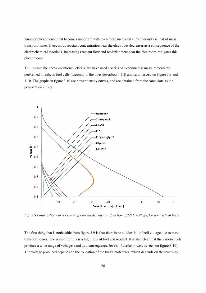
56
Another phenomenon that becomes important with even more increased current density is that of mass
transport losses. It occurs as reactant concentration near the electrodes decreases as a consequence of the
electrochemical reactions. Increasing reactant flow and replenishment near the electrodes mitigates this
phenomenon.
To illustrate the above-mentioned effects, we have used a series of experimental measurements we
performed on silicon fuel cells (identical to the ones described in [I]) and summarized on figure 3.9 and
3.10. The graphs in figure 3.10 are power density curves, and are obtained from the same data as the
polarization curves.
Fig. 3.9 Polarization curves showing current density as a function of MFC voltage, for a variety of fuels.
The first thing that is noticeable from figure 3.9 is that there is no sudden fall of cell voltage due to mass
transport losses. The reason for this is a high flow of fuel and oxidant. It is also clear that the various fuels
produce a wide range of voltages (and as a consequence, levels of useful power, as seen on figure 3.10).
The voltage produced depends on the oxidation of the fuel’s molecules, which depends on the reactivity

57
of the chemical bonds and the adsorption of the molecules on the anode catalyst. Often, but not always,
larger molecules are less likely to adsorb. The odd behavior of isopropanol can be explained by the fact
that oxygen located in the middlemost carbon of the isopropanol molecule polarizes the C-O bonds
making the oxygen very reactive and as consequence aldehyde (aceton) is readily formed resulting in the
observed high currents [130]. Aceton also poisons the catalyst, which is why the polarization curve
(figure 3.9) has a fold-back as voltage decreases [131].
Fig. 3.10: Polarization curves showing power density as a function of MFC voltage, for a variety of fuels.
3.3.2 Cyclic voltammetry (CV)
Cyclic voltammetry (CV) has been used in electrochemistry since the beginning of the 20th century to
study phenomena such as mass transport effects, adsorption and desorption of species on electrode
surfaces, catalytic activity etc. Typically, in the case of fuel cells where a separate reference electrode

58
does not exist, the measurement is similar to that for polarization curves, except that once the potential
has reached a set (low) value, e.g. 0.1 V, the voltage is increased until it reaches OCV again, i.e. the
direction of the voltage sweep is reversed. This ramp-down and ramp-up of the voltage can be repeated
multiple times. Figure 3.11 shows a graph of a CV measurement [III]. In this case the voltage was swept
from OCV to 0.05 V and back to OCV.
Fig. 3.11: Graph of a cyclic voltammetry (CV) measurement. The hysteresis in this CV curve is indicativeof the amount of water condensation at the cathode. Modified from on [III].
3.3.3 Chronoamperometric and -potentiometric measurements
Chronoamperometric characterization measures the current density and chronopotentiometric measures
the voltage of a cell during a period of hours or days. It is performed by holding the voltage (or the
current) at a constant value, and measuring the current (or the voltage).

59
Fig. 3.12: A multi-hour chronoamperometric measurement of a hydrogen-fueled MFC. Based on [III].
Chronoamperometric and chronopotentiometric measurements validate the fuel cell for long-term
operation. It is a very useful technique for the characterization of the fuel cell in an equilibrium state.
3.3.4 Electrochemical impedance spectroscopy (EIS)
In EIS, an alternate current or voltage component of variable frequency, is added to the output current or
voltage of the potentiostat: the frequency is swept from a pre-configured high to low value (typically from
hundreds of kHz to mHz), thus characterizing the complex equivalent impedance of the fuel cell. With
EIS we can study both the ohmic losses as well as the activation and mass transport losses of the fuel cell.
60
4. Novel approaches to microfabrication of fuel cells
4.1 MFCs with silicon nanograss (publications I, II and III)
Any micro-and/or macroporous material can work as a GDL in a MFC, as long as it is easy to
microfabricate or integrate with microfabricated flowfields. If it is made of a conductive material, a
separate current collector is not necessary. Highly doped silicon can be sufficiently conductive for this
purpose, and can be made porous either by electrochemical etching, or by RIE etching. In the latter case
silicon nanograss is produced. Silicon nanograss (also known as “black silicon”) is a quasi-regular field of
needle-like silicon structures, where the base of the needles is up to a few hundred nm in diameter
(typically ~100 nm), while the height can be up to a few μm. RIE processing of silicon often produces
silicon nanograss, either by increasing the flow rate of passivating gases such as O2, or by
resputtering/redeposition of contaminating nano-sized masking material particles [34]. The phenomenon
of silicon nanograss formation in SF6 RIE etching of silicon was observed as early as 1987 [132], and it is
usually considered an unwanted occurrence. The needle-like array absorbs visible light very efficiently,
giving it the alternative name “black silicon”.
Table 4.1 lists the RIE parameters used for etching silicon alongside the parameters for black silicon
formation, utilized for the silicon microfabrication in [I], [II], [III], and [IV]. The equipment used was
Oxford Plasmalab System 100 cryogenic ICP RIE. The anisotropic etch rate of silicon using the
parameters listed in Table 4.1 was ~7μm/min.
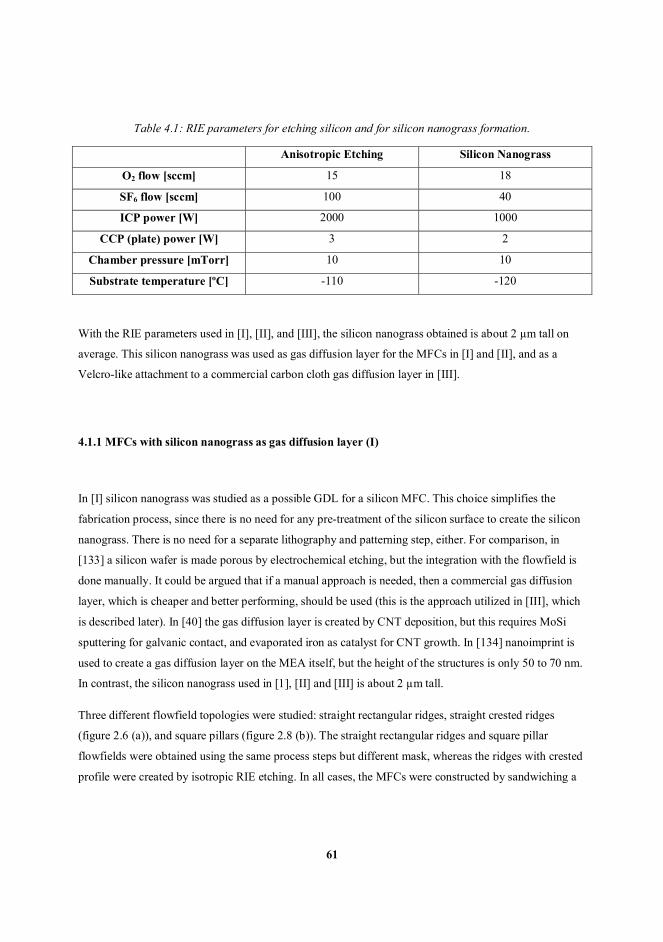
61
Table 4.1: RIE parameters for etching silicon and for silicon nanograss formation.
Anisotropic Etching Silicon Nanograss
O2 flow [sccm] 15 18
SF6 flow [sccm] 100 40
ICP power [W] 2000 1000
CCP (plate) power [W] 3 2
Chamber pressure [mTorr] 10 10
Substrate temperature [ºC] -110 -120
With the RIE parameters used in [I], [II], and [III], the silicon nanograss obtained is about 2 μm tall on
average. This silicon nanograss was used as gas diffusion layer for the MFCs in [I] and [II], and as a
Velcro-like attachment to a commercial carbon cloth gas diffusion layer in [III].
4.1.1 MFCs with silicon nanograss as gas diffusion layer (I)
In [I] silicon nanograss was studied as a possible GDL for a silicon MFC. This choice simplifies the
fabrication process, since there is no need for any pre-treatment of the silicon surface to create the silicon
nanograss. There is no need for a separate lithography and patterning step, either. For comparison, in
[133] a silicon wafer is made porous by electrochemical etching, but the integration with the flowfield is
done manually. It could be argued that if a manual approach is needed, then a commercial gas diffusion
layer, which is cheaper and better performing, should be used (this is the approach utilized in [III], which
is described later). In [40] the gas diffusion layer is created by CNT deposition, but this requires MoSi
sputtering for galvanic contact, and evaporated iron as catalyst for CNT growth. In [134] nanoimprint is
used to create a gas diffusion layer on the MEA itself, but the height of the structures is only 50 to 70 nm.
In contrast, the silicon nanograss used in [1], [II] and [III] is about 2 μm tall.
Three different flowfield topologies were studied: straight rectangular ridges, straight crested ridges
(figure 2.6 (a)), and square pillars (figure 2.8 (b)). The straight rectangular ridges and square pillar
flowfields were obtained using the same process steps but different mask, whereas the ridges with crested
profile were created by isotropic RIE etching. In all cases, the MFCs were constructed by sandwiching a

62
PEM between two silicon chips with flowfields, gas inlets and black silicon as GDL – figure 4.1. This
assembly was clamped between two aluminium plates of the measurement jig (seen in figure 3.7).
Fig. 4.1: Construction of the silicon MFC. Based on [I].
The chips were microfabricated from a thermally oxidized, highly boron-doped (ρ=0.01 Ω cm)
monocrystalline silicon wafers. The process flow is described in figure 4.2: the first photomask defines
the flowfield area by patterning the thermal oxide with photolithography and etching in buffered HF
(BHF). Next, photoresist is patterned using the flowfield photomask. The flowfield is created by etching
the wafer in ICP RIE using the parameters from Table 2 (“Anisotropic Etching”). Since this step is
performed at cryogenic temperatures, a 0.5 μm thick photoresist was chosen (AZ 1505) for this step, as it
is less likely to crack at low temperatures, compared to thicker diazoquinone-novolac resists. After the
silicon etching, the resist was removed and 200 nm of aluminium was sputtered on the back of the wafer
(the equipment was Oxford Plasmalab System 400 magnetron sputter) and patterned with lithography and
aluminium etching in H3PO4-based etchant, to define the inlet holes. The aluminium layer acted as a mask
for a DRIE through-wafer etch with the same RIE parameters as for the flowfield etch. The duration of
this etch step depended on the thickness of the wafers – about 75 min for a 525 μm thick wafer. Finally,
silicon nanograss is formed on the flowfield (the area not protected by the thermal oxide) and 40 nm of
chromium is sputtered over it. The function of the thin layer of chromium is to protect silicon nanograss
from corrosion during MFC use.

63
The MEAs used in this work were prepared by spray-coating the catalysts on Nafion® membranes using
a process described in subsection 2.5.
Fig. 4.2: Process flow for the microfabrication of a MFC with silicon nanograss GDL.
The MFCs described in [I] were initially tested with hydrogen gas as fuel, but later it was found that they
can be also fueled with a 2M solution of methanol. Both polarization (figure 4.3) and
chronoamperometric (figure 4.4) measurements were obtained. The only difference between the hydrogen
and the methanol-fueled devices is the catalyst on the anode side of the PEM: in case of hydrogen, this is
pure platinum, while for methanol a platinum-rutenium alloy was used, to avoid catalyst poisoning by
carbon monoxide.
The reactant gases (hydrogen and oxygen) were flowing at a rate of 50 mL/min, while the methanol
solution was flowing at a rate of 60 μL/min. The voltage was swept from OCV to 0.1 V at a rate of 1
mV/s using an Autolab PGSTAT potentiostat. Polarization curves for both fuels were taken before and
after a 72 hour chronoamperometric measurement. Maximum power and current density, as well as OCV
were higher in the case of hydrogen fuel. However, while the hydrogen-fueled cell shows performance
degradation after the chronoamperometric measurement, the methanol-fueled cell has slightly improved
current and power densities. This is attributed to improved humidification of the Nafion® membrane
during the 72-hour measurement with methanol. The chronoamperometric measurements (figure 4.4)
were done with voltage kept at E = 0.6 V in the case of hydrogen fuel, and E = 0.3 V in the case of

64
methanol. The hydrogen-fueled MFC appears to suffer from catalyst de-activation, but it is unclear at this
point the cause of this.
(a) (b)
Fig. 4.3: Polarization curves obtained with (a) hydrogen and (b) methanol as fuels for the siliconnanograss MFC. While the performance of the hydrogen-fueled cell decreases after the 72 hchronoamperometric measurement, in the case of methanol the opposite is true. Even so, the hydrogen-fueled cell produces higher current and power densities than the methanol-fueled one.
Fig. 4.4: Chronoamperometric measurement results for the silicon nanograss MFC. The hydrogen-fueledcells exhibit a higher performance loss, compared to the methanol-fueled ones.

65
Using the same silicon nanograss MFC, measurements with other liquid fuels were also realized.
Polarization curves obtained during these experiments are visible on figures 3.9 and 3.10.
An interesting result of the study published in [I] is also that the use of sputtered chromium (instead of
noble metals such as platinum) is an acceptable option for protecting the silicon current collecting surface.
This is in sharp contrast with most other authors who use gold for this purpose [40] [42] [43] [44] [54]
(~200 nm). Some authors have deposited 200 nm thick platinum layers on the silicon flowfield [134].
Using chromium instead of noble metals brings substantial costs savings at no loss in functionality or
performance. Furthermore, to create an effective current collector, the gold metallization of competing
designs has to be substantial (at least 100 nm) and sometimes extremely thick, such as in [40] (3 μm) or in
[133] (1 μm). Alternatively, some authors use commercial gold meshes as current collectors [102]. In [I]
– [III], thick metallization layers are not needed, because the highly-doped silicon chip takes the role of
both flowfield and current collector.
The MFCs described in [I] were used as a characterization platform for few-walled nanotube-supported
PtRu catalyst [135].
4.1.2 Stackable silicon MFC (II)
In publication [II], the silicon nanograss MFCs were modified in such a way as to allow for the simple
construction of a fuel cell stack. By simply changing the placement of inlet holes and flowfield topology,
it was possible to flow the reactant gases (hydrogen and oxygen) either from one flowfield to the next —
in series (figure 4.5 (a)), or to all flowfields at once — in parallel (figure 4.5 (b)). To characterize these
MFCs, the jig from Fig. 3.7 had to be modified, since the inlet holes are now in a different position
compared to the non-stackable MFCs (Fig. 4.5 (c)).
When stacking the silicon microfluidic chips in this way, it was found that leaking can be a problem. This
could be, perhaps, solved by using a gasketing material such as PDMS. The leaking could be decreased to
some extent by tightening the jig with more force, but this leads easily to cracking of the silicon chips.
Using less fragile yet conducting materials, such as metals, would allow for the stack to be compressed
with higher force.

66
Fig. 4.5: Schematic of stackable silicon nanograss MFCs. (a) serial gas flow. (b) parallel gas flow. Basedon [II]. (c) Photograph of the jig used for characterizing the stackable MFCs.
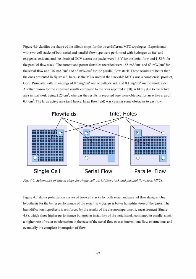
67
Figure 4.6 clarifies the shape of the silicon chips for the three different MFC topologies. Experiments
with two-cell stacks of both serial and parallel flow type were performed with hydrogen as fuel and
oxygen as oxidant, and the obtained OCV across the stacks were 1.6 V for the serial flow and 1.52 V for
the parallel flow stack. The current and power densities recorded were 155 mA/cm2 and 63 mW/cm2 for
the serial flow and 107 mA/cm2 and 43 mW/cm2 for the parallel flow stack. These results are better than
the ones presented in figure 4.3, because the MEA used in the stackable MFCs was a commercial product,
Gore Primea©, with Pt loadings of 0.3 mg/cm2 on the cathode side and 0.1 mg/cm2 on the anode side.
Another reason for the improved results compared to the ones reported in [II], is likely due to the active
area in that work being 2.25 cm2, whereas the results in reported here were obtained for an active area of
0.4 cm2. The large active area (and hence, large flowfield) was causing some obstacles to gas flow.
Fig. 4.6: Schematics of silicon chips for single cell, serial flow stack and parallel flow stack MFCs.
Figure 4.7 shows polarization curves of two-cell stacks for both serial and parallel flow designs. One
hypothesis for the better performance of the serial flow design is better humidification of the gases. The
humidification hypothesis is reinforced by the results of the chronoamperometric measurement (figure
4.8), which show higher performance but greater instability of the serial stack, compared to parallel stack:
a higher rate of water condensation in the case of the serial flow causes intermittent flow obstructions and
eventually the complete interruption of flow.

68
Fig. 4.7: Polarization curves of two-cell silicon MFCs stacks with serial flow (blue) and parallel flow(red).
Fig. 4.8: Chronoamperometric curves of two-cell silicon MFCs stacks with serial flow (blue) and parallelflow (red).
4.1.3 Silicon MFCs with silicon nanograss for integration of commercial gas diffusion layer (III)
Silicon nanograss can be used to integrate thick commercial gas diffusion layers (GDL) with silicon
MFCs. For the purpose of this integration, the silicon chips had to have a basin in which the GDLs could

69
fit (figure 4.9). The silicon nanograss’ function was to increase the galvanic conductivity between the
silicon chips and the GDL.
Fig. 4.9: Construction of the MFC with integrated gas diffusion layers with silicon nanograss aselectrical contact promoter. Based on [III].
The main idea of the device is that black silicon needles would penetrate into the carbon cloth or carbon
felt GDL, increasing contact area (figure 4.10).
Fig. 4.10: Schematic representation of black silicon (in cyan) piercing into a carbon felt GDL.

70
The process flow for the realization of the silicon chips for this new device is very similar to the one
where silicon nanograss functions as GDL. In fact only one additional step is needed; the sinking of the
entire flowfield before backside inlet etch and black silicon formation.
The process flow, as detailed in [III], calls for a flowfield metallization layer composed of 40 nm of gold
sputtered over 10 nm of Ti-W adhesion layer. This choice was purely out of necessity, since the
sputtering device with the chromium target was unavailable at the time.
To better understand how silicon nanograss helps with integration of commercial GDL layers, one should
get familiar with the structure of a typical commercial GDL such as carbon cloths and carbon felts: these
are carbonized fibrous layers, around 100 μm thick, into which carbon black was printed, spray-painted or
squegeed. The carbon black is present on one side of the GDL and it may or may not contain platinum or
other catalyst. The side of the GDL where carbon black is present, is microporous, while the other side
where only the fibrous support structure exists, is macroporous (figure 4.11).
Fig. 4.11: SEM images of carbon felt. Transversal view is one the left. The insets are top views of themicroporous side (up) and macroporous side (bottom). All images were obtained with the samemagnification.
The work in [III] not only demonstrated that adding silicon nanograss increased the performance of a
silicon MFC with commercial GDL layers inserted in the basins (figure 4.9), but it also showed that
silicon nanograss effectively increased the contact conductivity between a silicon chip and both the

71
microporous and the macroporous sides of the GDL. This increase is more marked when the silicon
nanograss is in contact with the microporous side, but to maximize a fuel cell’s performance, the
microporous side should be turned towards the catalyst layer of the MEA, so the silicon nanograss was
contacting the macroporous side when used in MFCs.
While using carbon cloth or carbon felt increases the performance of the micro fuel cells, the
experimentation with these devices is slightly more difficult than the ones presented in [I], as some minor
additional manual work is needed to position the felt in the chip’s basin. It is expected, however, that in
case of commercial production this action would be easily robotized. While the added step of placing the
carbon cloth or felt into the basin increases fabrication complexity slightly, it is well worth it since it
considerably improves the performance of the MFCs compared to the ones with silicon nanograss GDL
from [I]: the maximum power density obtained for the cells from [III] was 127 mW cm-2, compared to
69.2 mW cm-2 in [I]. Finally, it should be noted that the MFCs in [III] have shown stable performance
over a 20 h period with a minimum current density of 150 mA cm-2 — something very rarely found in
MFC literature.
4.2 Laser-ablated silicon MFCs (publication IV)
Microfabrication by laser ablation was covered in subsection 2.4. Overall, it can be said that shorter laser
pulses contribute to better feature quality and controllability, whereas longer pulses can increase the speed
of ablation i. e. the amount of removed material per unit time. The problem of re-deposited material is
more severe with longer laser pulses, but there can be microfluidic applications where this is not an issue.
The MFCs discussed in this thesis, whose construction is in principle described in figure 4.1, are just such
applications. In [IV], picosecond UV (15 ps, 355 nm) laser pulses were used to microfabricate MFC
silicon chips. Both the inlet holes and the flowfields were ablated in one pass.
Microfabrication by laser ablation is a very convenient prototyping technique – samples can be prepared
without lithography and the associated mask preparation. Furthermore, laser ablation of silicon with
picosecond pulses at UV wavelengths can be very efficient in terms of material removal rate and overall
processing speed, as evidenced by the results published in [IV]. The high-energy ablation with substantial
material removal, as used in [IV], has the drawback of producing rough and relatively un-even sidewalls,

72
and deposits some of the material at the top, near the grooves. It is fortunate that these imperfections are
not an impediment for the functioning of a MFC.
Two sets of laser ablation parameters were selected, which will be referred to “low energy pulses” and
“high energy pulses”, and are detailed in Table 4.2.
Table 4.2: Laser ablation process parameters, in [IV].
High energy pulses Low energy pulses
Pulse frequency 400 kHz 1 MHz
Average power 18.4 W 6.25 W
Pulse energy 46 μJ 6.25 μJ
To obtain the target depth of 50 μm, the laser beam with high energy pulses had to scan the length of the
channel 270 times, while with low energy pulses this had to be done 1000 times. The scan speeds were 4
m/s and 10 m/s for high and low energy pulse beams, respectively. Overall, using high energy pulses
increased the material removal rate considerably, because for each scan line the galvo scanner mechanics
must stop and reverse the direction of movement, and these actions consume about the same amount of
time regardless of the beam scan speed. Therefore, the decrease of repetitions from 1000 to 270 is a very
significant factor to reducing the overall processing time. The total processing time of a wafer containing
6400 1-cm long channels (64 MFC chips) took 2 h 29 min with low energy pulses, and only 58 min with
high energy pulses. Figure 4.12 shows SEM images of both low and high energy pulse ablated channels,
taken laterally and from the top. It is clear that the low energy-ablated channels have a more uniform
appearance, with fewer droplets, less redeposited material, and smoother sidewalls compared to the high
energy-ablated channels.
The high energy-ablated channels are also about twice as wide as the low energy-ablated ones. This was
taken into consideration when designing RIE-fabricated counterparts of the ablated MFC chips. This
experiment was done in order to compare laser-ablated MFC chips to RIE fabricated ones in terms of fuel
cell performance. The RIE-fabricated chips used a process flow which is identical to the one described in
subsection 4.1.1 (figure 4.2), save for the lack of a silicon nanograss step. The voltammetric sweeps and
chronoamperometric measurements performed with hydrogen as fuel and oxygen or air as oxidant,
showed that the MFCs constructed with laser-ablated chips have better performance than the RIE
fabricated counterparts. This may be due to the slanted sidewalls on which the sputtered chromium layer

73
is less likely to have discontinuities than on vertical sidewalls. The increased performance may be also
due to the triangular cross-section of the channels in the laser-ablated chips.
(a) (b)
(c) (d)
Fig. 4.12: SEM images of picoseconds-laser ablated channels with low energy pulses ((a) and (c)) andhigh energy pulses ((b) and (d)). (a) and (b) were taken laterally, (c) and (d) were taken from top.
The laser-ablated chips were also characterized with a micro-Raman setup (NT-MDT NTEGRA
Spectra®) to determine the stress induced in the crystalline silicon. Micro Raman spectroscopy as a non-
destructive and sensitive characterization method, has been previously used by other authors [136] [137]
[138] [139] to determine quantitatively and qualitatively the intrinsic stresses present in crystalline
silicon. Our research showed that the chips ablated with high energy pulses had far less intrinsic stresses

74
and smaller areas of amorphous silicon, compared to low energy-ablated chips. The most likely
explanation is that higher thermal energy deposited in the substrate per laser pulse promotes re-
crystallization and stress relaxation. The silicon wafers, after high-energy pulse ablation were too hot to
hold with bare hands, proving that a significant fraction of the laser beam energy was thermally deposited
in the wafer.
Figure 4.13 shows a micro-Raman map of grooves ablated with (a) high-energy and (b) low energy pulses
(table 4.2). Specifically, the position of the Si monocrystalline peak is charted. This peak is normally at
520 cm-1, but shifts depending on the stress. The shift to lower Raman frequencies (lower energies) is
indicative of tensile stress.
(a) (b)
Fig. 4.13:Micro-raman map of picosecond-laser ablated groove in silicon (a) at low pulse energies (400kHz repetition rate) and (b) at high pulse energies (1 MHz repetition rate).This map shows the position ofthe monocrystal Si (c-Si) peak, which is proportional to the stress induced in the lattice. From [IV].
All things considered, high energy ablation is more desirable than the low energy one, in this particular
application where sidewall smoothness and precise feature control is not critical.
The advantage of microfabrication by laser ablation is quick prototyping ability, and this advantage,
compared to traditional lithography-based microfabrication extends also to MFC research; where channel
and inlet hole position and topology can easily be modified for each cell or small batch of cells. High-
energy picosecond pulsed ablation like the one used in [IV] produces fast results, and while the edges of
the channels are jagged, this is not an issue for MFCs.

75
4.3 Bulk-aluminium MFCs (publication V)
In an effort to improve the mechanical robustness as well as the conductivity of MFC chips, research was
invested in bulk micromachining of 6061 aluminium alloy. A detailed study on deep etching of this alloy
is reported in [V], and an implementation of such technology to microfabricate a MFC is also presented.
Some of the results were mentioned in subsections 2.2 and 2.2.1. To surmise, 6061 alloy etching in
phosphoric acid-based etchant (74% H3PO4 and 2.5% HNO3 in water) at 50°C is isotropic (figure 2.6 (a))
and produces a rough surface (RMS roughness ~1 μm). The etch rate decreases and the roughness
increases as the etch time increases (figure 2.5). Both of these phenomena can be adequately explained by
the non-etchable alloying elements present in 6061 aluminium (e. g. silicon). The un-etched elements
produce a patina that can be removed with a water spray. Iliescu et al. have observed very similar
phenomena during wet etching of glass [140] [29].
The construction of the MFCs is identical to the one illustrated in figure 4.9. The starting point for the
aluminium chip microfabrication (figure 4.14) was a single-side polished, 800 μm thick 6061 aluminium
alloy wafer. Photoresist (either AZ 5214 or AZ 4562) was spinned on both sides of the wafer. The
polished side was selected as the top side on which the resist was patterned with photolithography to
define the basin areas. The resist on the back of the wafer protects it from etching. This is done to avoid
thinning the wafer and increasing the roughness on the side of the wafer that will be used as electrical
contact to the measurement jig. Etching in phosphoric acid-based etchant at 50°C produced the 50 μm
deep basins in which the commercial GDL was to be placed. The etching was done in a dedicated glass
beaker, to avoid contaminating the cleanroom equipment in common use with alloying elements such as
copper, iron, and zinc. After the basin etching, resist was spinned on the top side a second time: to
achieve an uninterrupted resist film on the already patterned surface, 4 mL of resist was pipetted on the
wafer, which was sufficient to completely cover the basins. After spinning, the resist was patterned with
photolithography to define the flowfield at the bottom of the basins. The flowfield was etched in the same
way as the basins. Finally, the resist was removed from both sides of the wafer, and 40 nm of chromium
was sputtered over the flowfield, for similar reasons as with the silicon MFCs.

76
Fig. 4.14: Process flow for the microfabrication of aluminium MFC chips. Based on [V].
The highly rough surface obtained with prolonged (t > 10 min) etching of 6061 aluminium may increase
the contact conductivity with the GDL inserted in the basins (figure 2.5 (a)), though this was not verified,
yet.
It is interesting to note that the rough surface seem to have a beneficial effect on photoresist adhesion, as
evidenced by SEM images in figure 4.15. The upper image shows two channels etched by spinning resist
on the polished side of a 6061 aluminium wafer. The curvature of the profiles near the top suggests that
some photoresist delamination occurred during etching. This is in contrast with the lower SEM image of a
flowfield etched on the bottom of a basin. The surface on which the resist was spinned was very rough,
and this roughness appears to have decreased delamination, as the profile of the pillars form a right angle
at the top.

77
Fig. 4.15: Features etched in 6061 aluminium alloy depending on surface roughness. Upper: polishedsurface. Lower: already etched surface (bottom of basin).
The aluminium MFCs were characterized with hydrogen as fuel and oxygen or air as oxidants. The results
with oxygen are reported in figure 4.16. With a maximum current density of 1.109 A/cm2 and a
maximum power density of 228 mW cm-2 (in addition to a minimum sustained and very stable current
density of 90 mA/cm2), these aluminium-based MFCs are the best performing hydrogen-fueled devices
currently found in MFC literature.

78
(a) (b)
Fig. 4.16: Performance of aluminium MFCs: (a) polarization curves and (b) chronoamperometricmeasurement. Based on [V].
Bulk aluminium microfabrication literature is very scarce, and to date, apart from [V], there has not been
a systematic research of the etching characteristics of aluminium alloys. The fact that the work in [V] also
demonstrates an application that greatly benefits of the use of the material – a record-setting MFC – gives
additional value to the article. The simplicity and low cost of the equipment and materials used in the
microfabrication is also notable, opening the door to inexpensive research in microfluidics.
79
5. Conclusions and outlook
The works presented in this thesis [I] - [V] are both a study on micro fuel cell implementation as well as
experiments with existing microfabrication technologies utilized in a new way in the domain of
microfluidics. For instance, silicon nanograss used as a gas diffusion layer (GDL), or as a contact layer to
a commercial GDL; through-wafer holes (vias) for gas distribution in stacked MFCs; high-speed ablated
channels – usually unsuitable for microfluidic devices – used in a microfluidic device sui generis; wet
etching of aluminium bulk instead of the common etching of aluminium thin films.
Using silicon nanograss as GDL makes it possible to have the flowfield, the GDL and the current
collector (as long as silicon is highly doped and therefore conductive) microfabricated from a single
silicon substrate. This is advantageous to miniaturization and to integration with other silicon MEMS or
electronic components. Using 400 μm thick silicon wafers, one could make a functional MFC that is less
than 1 mm thick.
Combining silicon nanograss as GDL with the stacking technology presented in [II] could enable the
creation of microscopic multicell stacks, due to the ease of miniaturizing the MFCs based on the process
presented in [I], and thanks to the fluidic topologies presented in [II] and this thesis, which do not require
tubing or fluidic channels.
MFC chips with a recessed flowfield with silicon nanograss on top can accommodate a plethora of
different porous and fuzzy materials that can act as diffusion layers. Biological materials, including gels,
could also be inserted in the basin and contacted via the silicon nanograss.
Using a high-energy picosecond laser system it is possible to microfabricate the flowfield and the inlet
holes in silicon MFC chips in one step and very fast, sacrificing sidewall smoothness and feature
uniformity. This high ablation speed combined with the fact that no photolithography steps are necessary,
makes MFC chip prototyping a viable proposition.
The limitations, or drawbacks, of the silicon picosecond laser ablation technique studied in [IV] are, in
addition to relatively poor feature uniformity and sidewall smoothness, a V-shaped channel profile, a
relatively large amount of re-deposited silicon on top of the ablated features, and a non-insignificant

80
thermal budget: the thermal energy delivered to the substrate is sufficient to raise its temperature above
the glass transition temperature of some polymers. Many of the abovementioned negative effects can be
decreased by using the low-energy ablation mode: sidewall smoothness and feature uniformity are
improved, and there is far fewer re-deposited material. Sadly, this ablation mode comes with its own set
of compromises, namely the slower ablation rate and the higher stresses induced in the ablated silicon
substrate. As was mentioned in subsection 2.4, using laser pulses of even shorter duration, such as
hundreds or tens of femtoseconds, ablation controllability becomes very high and thermal energy
delivered to the substrate is almost nil. Moreover, material redeposition is very little to none.
Unfortunately, high-energy femtosecond laser systems are still very expensive compared to pico-and-
nanosecond ones, and ablation speed is generally much lower.
The research in [V] basically broke the ground of patterned aluminium bulk microfabrication. While
aluminium as a substrate has some important advantages such as high electrical conductivity and
mechanical robustness, the highly rough etched surfaces make it a problematic choice for many fluidic
applications. However, it seems that aluminium and its alloys are the ideal material for MFC fabrication,
and there are other microfluidic applications that are still possible in spite of a 1 μm RMS roughness.
Moreover, the microfabrication process detailed in [V] does not require expensive cleanroom equipment
apart from the lithography aligner. This means, it could be a cheap option for microfluidic research in
places with insufficient economic resources for a advanced cleanroom setup.
The study of aluminium alloy bulk micromachining presented in [V] lays out a set of limitations as well:
the high roughness of the etched surfaces is one, but there is the more general issue of isotropically etched
features, which have a circular or elliptical profile. High aspect ratio features are not possible. The
substrate material itself, without a passivation layer, is incompatible with many inorganic solutions, both
alkaline and acidic. The passivation layer used in the MFCs described in [V] is a 40 nm thick layer of
sputtered chromium. Other chemically stable metals such as nickel, platinum, palladium, gold or tungsten
(or an alloy thereof) could also be used. Another issue that limits applicability of bulk aluminium
microfabrication to microfluidics is the lack of established bonding techniques. For this purpose, adhesive
bonding seems the most promising candidate.
It should be borne in mind that the works reported in [IV] and [V] have potentially a more general value
for MEMS than just MFC or microfluidics. [IV] is a detailed account on how to achieve high-speed laser
ablation of silicon while having low induced stresses and still sufficient (for the application) structure
quality: uniformity, smoothness, amount of redeposited material. The article includes a detailed micro-
Raman characterization of the ablated channels, with an original method for quantifying the disorder-ness

81
(deviation from crystallinity) of the silicon lattice. [V] is a detailed scientific study about aluminium alloy
etching. The information contained there can be used as guidelines for planning of microfabrication
processes that use aluminium alloys as bulk material. If the limitations of the techniques are taken into
consideration, and are acceptable for a given application, then [IV] and [V] are valuable contributions to
the field of microfabrication, extending its toolbox.
Going forward, the work presented in [I] [II] [III] could be extended in two directions: further
miniaturization and integration of silicon MFCs with MEMS or electronic components and integration of
GDLs not typically used in microfabrication, with silicon MFCs. The perspectives of further research
extending the work in [IV] are centered around fast prototyping of microfluidic devices tolerant of V-
shaped grooves, less than ideal feature size control and redeposited material. Finally, the work started
with [V] should be continued with research in bonding of substrates, experiments with new etchant
formulations which would decrease or eliminate etched surface roughness, experiments aimed at
increasing photoresist adhesion, and verification of various passivation layers for specific microfluidic
applications of aluminium chips.
Micro fuel cells, primary and secondary (rechargeable) batteries, and super capacitors are, to a large
extent, competing technologies as they all try to support various mobile applications. While some micro
fuel cell implementations may be better positioned as implantable micro-power sources, it is not clear
whether they can also replace the more traditional primary and secondary batteries used in cell phones,
tablets and laptops, in the long run. It is however important to note that the micro-and-nanotechnologies
developed to improve either of these power sources, usually benefit all the other technologies as well. For
that reason, regardless of which technology ends up being the dominant power source for mobile
application, no research is wasted and all MEMS and nanotechnology researchers are contributing to that
technology, either directly or indirectly. In that sense, all this research is a good use of science.

82
References
[1] G. W. A. Dummer, "Component Development in the United Kingdom," in Electronic ComponentsSymposium, Washington DC, 1952.
[2] Robert N. Noyce, "Semiconductor device-and-lead structure," US2981877A, July 30, 1959.
[3] Harvey C. Nathanson, William E. Newell, Robert A. Wickstrom, and John R. Davis, "The resonantgate transistor," IEEE T. Electron. Dev., vol. 14, no. 3, pp. 117 - 133, March 1967.
[4] A C M Gieles and G H J Somers, "Miniature pressure transducers with a silicon diaphragm,"Philips Tech. Rev., vol. 33, pp. 14–20, 1973.
[5] K E Petersen, "Fabrication of an integrated, planar silicon ink-jet structure," IEEE Trans. ElectronDevices, vol. 26, pp. 1918-1920, 1979.
[6] K E Petersen, "Silicon as a Mechanical Material," Proc. IEEE, vol. 70, no. 5, pp. 420-457, May1982.
[7] Marc J Madou, Fundamentals of Microfabrication: The Science of Miniaturization, 2nd ed.: CRCPress, 2002.
[8] S C Terry, J H Jerman, and J B Angell, "A gas chromatographic air analyzer fabricated on a siliconwafer," IEEE T. Electron. Dev., vol. 26, no. 12, pp. 1880-1886, 1979.
[9] A V Pattekar and M V Kothare, "A microreactor for hydrogen production in micro fuel cellapplications," J. Microelectromech. S., vol. 13, no. 1, pp. 7-18, 2004.
[10] R Hahn, S Wagner, A Schmitz, and H Reichi, "Development of a planar micro fuel cell with thinfilm and micro patterning technologies," J. Power Sources, vol. 131, no. 1-2, pp. 73-78, May 2004.
[11] Erik Kjeang, Ned Djilali, and David Sinton, "Microfluidic fuel cells: A review," J. Power Sources,vol. 186, no. 2, pp. 353-369, January 2009.
[12] V V Zhivonitko et al., "Remote detection NMR imaging of gas phase hydrogenation in microfluidicchips," Lab Chip, vol. 13, no. 8, pp. 1554-1561, March 2013.
[13] A Kundu et al., "Micro-fuel cells - current development and applications," J. Power Sources, vol.170, no. 1, pp. 67-78, 2007.
[14] G Wu, D Xu, B Xiong, and Y Wang, "A high-performance bulk mode single crystal silicon

83
microresonator based on a cavity-SOI wafer," J. Micromech. Microeng., vol. 22, no. 2, pp. 025020-8, February 2012.
[15] S E Alper and T Akin, "A Single-Crystal Silicon Symmetrical and Decoupled MEMS Gyroscopeon an Insulating Substrate," J. Microelectromech. S., vol. 14, no. 4, pp. 707-717, August 2005.
[16] S M Barnes, S L Miller, M S Rodgers, and F Bitsie, "Torsional Ratcheting Actuating System," in2000 International Conference on Modeling and Simulation of Microsystems, San Diego, CA,USA, 2000, pp. 273 - 276.
[17] Kirt R. Williams and Richard S. Muller, "Etch rates for Micromachining Processing," J.Microelectromech. S., vol. 5, pp. 256-269, December 1996.
[18] Kirt R Williams, Kishan Gupta, and Matthew Wasilik, "Etch Rates for Micromachining Processing- Part II," J. Microelecromech. Syst., vol. 12, no. 6, pp. 761-778, December 2003.
[19] Chang Liu, "Recent Developments in Polymer MEMS," Adv. Mater., vol. 19, pp. 3783-3790, 2007.
[20] Edgar D Goluch et al., "A bio-barcode assay for on-chip attomolar-sensitivity protein detection,"Lab Chip, vol. 6, pp. 1293-1299, August 2006.
[21] Mehran Mehregany, Christian A Zorman, Narayanan Rajan, and Chien Hung Wu, "Silicon CarbideMEMS for Harsh Environments," Proc. IEEE, vol. 86, no. 8, pp. 1594-1610, August 1998.
[22] Walter Smetana et al., "A multi-sensor biological monitoring module built up in LTCC-technology," Microelectron. Eng., vol. 84, pp. 1240-1243, 2007.
[23] M. Wayne Moreau, Semiconductor Lithography - Principles, Practices, and Materials. New York,USA: Plenum Press, 1988.
[24] A. Del Campo and C Greiner, "SU-8: a photoresist for high-aspect-ratio and 3D submicronlithography," J. Micromech. Microeng., vol. 17, pp. R81-R95, 2007.
[25] J P Esquivel et al., "Towards a compact SU-8 micro-direct methanol fuel cell," J. Power Sources,vol. 195, pp. B110-B115, 2010.
[26] K. J. Owen, B. VanDerElzen, R. L. Peterson, and K. Najafi, "High Aspect Ratio Deep SiliconEtching," in MEMS 2012, Paris, France, 2012, pp. 251-254.
[27] K Biswas and S Kal, "Etch characteristics of KOH, TMAH and dual doped TMAH for bulkmicromachining of silicon," Microelectron. J., vol. 37, no. 6, pp. 519-525, June 2006.
[28] E D Palik, O J Glembocki, I Heard, P S Burno, and L Tenerz, "Etching roughness for (100) siliconsurfaces in aqueous KOH," J. Appl. Phys., vol. 70, no. 6, pp. 3291-3300, 1991.

84
[29] Ciprian Iliescu, Francis E.H. Tay, and Jianmin Miao, "Strategies in deep wet etching of Pyrexglass," Sens. Actuators A, vol. 133, pp. 395-400, 2007.
[30] Kristian P Larsen, Dirch H Petersen, and Ole Hansen, "Study of the Roughness in a PhotoresistMasked, Isotropic, SF6-Based ICP Silicon Etch," J. Electrochem. Soc., vol. 153, no. 12, pp. G1051-G1058, 2006.
[31] Gianmario Scotti, Petri Kanninen, Tanja Kallio, and Sami Franssila, "Symmetric silicon micro fuelcell with porous electrodes," in Transducers 2009, Denver, CO, USA, 2009, pp. 1401-1404.
[32] (2013, October) Reactive Ion Etching (RIE) Oxford Instruments. [Online]. http://www.oxford-instruments.com/products/etching-deposition-and-growth/plasma-etch-deposition/rie
[33] H V Jansen, M J de Boer, S Unnikrishnan, M C Louwerse, and M C Elwenspoek, "Black siliconmethod: X. A review on high speed and selective plasma etching of silicon with profile control: anin-depth comparison between Bosch and cryostat DRIE processes as a roadmap to next generationequipment," J. Micromech. Microeng., vol. 19, p. 033001, 2009.
[34] Henri Jansen, Meint de Boer, Rob Legtenberg, and Miko Elwenspoek, "The black silicon method: auniversal method for determining the parameter setting of a fluorine-based reactive ion etcher indeep silicon trench etching with profile control," J. Micromech. Microeng., vol. 5, pp. 115-120,1995.
[35] J. W. Coburn and H. F. Winters, "Ion and electron-assisted gas-surface chemistry—An importanteffect in plasma etching," J. Appl. Phys., vol. 50, no. 5, pp. 3189-3196, May 1979.
[36] Veikko Lindroos, Markku Tilli, Ari Lehto, and Teruaki Motooka, Handbook of silicon basedMEMS materials and technology.: Elsevier Inc., 2010.
[37] Meint J de Boer et al., "Guidelines for Etching Silicon MEMS Structures Using Fluorine High-Density Plasmas at Cryogenic Temperatures," J. Microelectromech. S., vol. 11, no. 4, pp. 385-401,August 2002.
[38] R. Dussart et al., "Silicon columnar microstructures induced by an SF6/O2 plasma," J. Phys. D.,vol. 38, pp. 3395-3402, September 2005.
[39] L. Sainiemi et al., "Non-Reflecting Silicon and Polymer Surfaces by Plasma Etching andReplication," Adv. Mater., vol. 23, pp. 122-126, 2011.
[40] Nariaki Kuriyama, Tadahiro Kubota, Daisuke Okamura, Toshifumi Suzuki, and Jun Sasahara,"Design and Fabrication of MEMS-Based Monolithic Fuel Cells," Sens. Actuators A, vol. 145-146,pp. 354-362, July 2008.
[41] Kyong-Bok Min, Shuji Tanaka, and Masayoshi Esashi, "Fabrication of novel MEMS-basedpolymer electrolyte fuel cell architectures with catalytic electrodes supported on porous SiO2," J.
85
Micromech. Microeng., vol. 16, pp. 505–511, 2006.
[42] J. D. Morse et al., "A MEMS-based reformed methanol fuel cell for portable power," J. Micromech.Microeng., vol. 17, pp. S237–S242, 2007.
[43] J Yeom et al., "Microfabrication and characterization of a silicon-based millimeter scale, PEM fuelcell operating with hydrogen, methanol, or formic acid," Sens. Actuators B, vol. 107, no. 2, pp. 882-891, June 2005.
[44] Scott Gold, Kuan-Lun Chu, Chang Lu, Mark A. Shannon, and Richard I. Masel, "Acid loadedporous silicon as a proton exchange membrane for micro-fuel cells," J. Power Sources, vol. 135,no. 1-2, pp. 198-203, September 2004.
[45] Neuss Sabatè et al., "New approach for batch microfabrication of silicon-based micro fuel cells,"Microsyst. Technol., vol. DOI 10.1007/s00542-013-1781-4, March 2013.
[46] S C Kelley, G A Deluga, and W H Smyrl, "A Miniature Methanol/Air Polymer Electrolyte FuelCell," Electrochem. Solid State Lett., vol. 3, no. 9, pp. 407-409, July 2000.
[47] Walter Lang, "Silicon microstructuring technology," Mater. Sci. Eng., vol. R17, pp. 1-55, 1996.
[48] Sami Franssila, Introduction to Microfabrication.: John Wiley & Sons, Ltd., 2004.
[49] Kenji Tokoro, Daisuke Uchikawa, Mitsuhiro Shikida, and Kazuo Sato, "Anisotropic etchingproperties of silicon in KOH and TMAH solutions," in International Symposium onMicromechatronics and Human Science, Nagoya, Japan, 1998, pp. 65-70.
[50] Chelsey D. Baertsch et al., "Fabrication and structural characterization of self-supporting electrolytemembranes for a micro solid-oxide fuel cell," J. Mater. Res., vol. 19, no. 09, pp. 2604-2615, 2004.
[51] Hong Huang et al., "High-Performance Ultrathin Solid Oxide Fuel Cells for Low-TemperatureOperation," J. Electrochem. Soc., vol. 154, no. 1, pp. B20-B24, 2007.
[52] T Pichonat, B Gauthier-Manuel, and D Hauden, "A new proton-conducting porous siliconmembrane for small fuel cells," Chem. Eng. J., vol. 101, pp. 107-111, 2004.
[53] K Shah, W C Shin, and R S Besser, "Novel microfabrication approaches for directly patterningPEM fuel cell membranes," J. Power Sources, vol. 123, pp. 172-181, 2003.
[54] S J Lee et al., "Design and fabrication of a micro fuel cell array with ‘‘flip-flop’’ interconnection,"J. Power Sources, vol. 112, pp. 410-418, 2002.
[55] Jeffrey D Morse, Alan F Jankowski, Robert T Graff, and Jeffrey P Hayes, "Novel proton exchangemembrane thin-film fuel cell for microscale energy conversion," J. Vac. Sci. Technol. A, vol. 18,pp. 2003-2005, 2000.

86
[56] Grigoras Kestutis, Veli-Matti Airaksinen, and Sami Franssila, "Coating of Nanoporous Membranes:Atomic Layer Deposition Versus Sputtering," J. Nanosci. Nanotechnol., vol. 8, no. 12, p. 1.8, 2008.
[57] Youngcheol Joo, Hsin-Chih Tim Yeh, Kiet Dieu, and Chang-Jin Kim, "Air cooling of amicroelectronic chip with diverging metal microchannels monolithically processed using a singlemask," J. Micromech. Microeng., vol. 18, no. 11, pp. 115022-13, 2008.
[58] Shou-Shing Hsieh, Chih-Lun Feng, and Ching-Feng Huang, "Development and performanceanalysis of a H2/air micro PEM fuel cell stack," J. Power Sources, vol. 163, pp. 440-449, 2006.
[59] L Zhu et al., "An on-demand microfluidic hydrogen generator with self-regulated gas generationand self-circulated reactant exchange with a rechargeable reservoir," Microfluid. Nanofluid., vol.11, pp. 569-578, 2011.
[60] Ian W Boyd and John I B Wilson, "Laser processing of silicon," Nature, vol. 303, pp. 481-486,June 1983.
[61] U M Mescheder et al., "Local laser bonding for low temperature budget," Sens. Actuators A, vol.97-98, pp. 422-427, 2002.
[62] T Otani, L Herbst, M Heglin, S V Govorkov, and A O Wiessner, "Microdrilling andmicromachining with diode-pumped solid-state lasers," Appl. Phys. A, vol. 79, no. 4-6, pp. 1335-1339, 2004.
[63] M R H Knowles, G Rutterford, D Karnakis, and A Ferguson, "Micro-machining of metals, ceramicsand polymers using nanosecond lasers," Int. J. Adv. Manuf. Technol., vol. 33, pp. 95-102, 2007.
[64] W Hu, Y C Shin, and G B King, "Micromachining of Metals, Alloys, and Ceramics by PicosecondLaser Ablation," J. Manuf. Sci. Eng., vol. 132, p. 011009, 2010.
[65] P R Herman et al., "Laser shaping of photonic materials: deep-ultraviolet and ultrafast lasers," Appl.Surf. Sci., vol. 154-155, pp. 577-586, February 2000.
[66] Matthew A Roberts, Joël S Rossier, Paul Bercier, and Hubert Girault, "UV Laser MachinedPolymer Substrates for the Development of Microdiagnostic System," Anal. Chem., vol. 69, pp.2035-2042, 1997.
[67] Ajit P Joglekar, Hsiao-hua Liu, Edgar Meyhöfer, Gerard Mourou, and Alan J Hunt, "Optics atcritical intensity: Applications to nanomorphing," PNAS, vol. 101, no. 16, pp. 5856-5861, April2004.
[68] V Craciun et al., "Laser-induced explosive boiling during nanosecond laser ablation of silicon,"Appl. Surf. Sci., vol. 186, no. 1-4, pp. 288-292, January 2002.
[69] M Lenzner et al., "Femtosecond Optical Breakdown in Dielectrics," Phys. Rev. Lett., vol. 80, no.

87
18, pp. 4076-4079, May 1998.
[70] Quanming Lu, Samuel S Mao, Xianglei Mao, and Richard E Russo, "Delayed phase explosionduring high-power nanosecond laser ablation of silicon," Appl. Phys. Lett., vol. 80, pp. 3072-3074,April 2002.
[71] H W K Tom, G D Aumiller, and C H Brito-Cruz, "Time-Resolved Study of Laser-Induced Disorderof Si Surfaces," Phys. Rev. Lett., vol. 60, no. 14, pp. 1438-1441, April 1988.
[72] S K Sundaram and E Mazur, "Inducing and probing non-thermal transitions in semiconductorsusing femtosecond laser pulses," Nat. Mater., vol. 1, pp. 217-224, December 2002.
[73] R. Stoian, D. Shkenasi, A. Rosenfeld, and E. E. B. Campbell, "Coulomb explosion in ultrashortpulsed laser ablation of Al2O3," Phys. Rev. B, vol. 62, no. 19, pp. 13167–13173, 2000.
[74] S. Paul, S. I. Kudryashov, K. Lyon, and S. D. Allen, "Nanosecond-laser plasma-assisted ultradeepmicrodrilling of optically opaque and transparent solids," J. Appl. Phys., vol. 101, no. 4, pp.043106-8, February 2007.
[75] O Guillot-Noël, R Gomez-San Roman, and J Perrière, "Growth of apatite lms by laser ablation:Reduction of the droplet areal density," J. Appl. Phys., vol. 80, no. 3, pp. 1803-1808, August 1996.
[76] Adela Ben-Yakar and Robert L Byer, "Femtosecond laser ablation properties of borosilicate glass,"J. Appl. Phys., vol. 96, no. 9, pp. 5316-5323, November 2004.
[77] D Du, X Liu, G Korn, J Squier, and G Morou, "Laser-induced breakdown by impact ionization inSiO2 with pulse widths from 7 ns to 150 fs," Appl. Phys. Lett., vol. 64, no. 23, pp. 3071-3073, June1994.
[78] B C Stuart et al., "Nanosecond-to-femtosecond laser-induced breakdown in dielectrics," Phys. Rev.B, vol. 53, pp. 1749-1761, 1996.
[79] S Moore and D Erickson, "A plate-frame flow-through microfluidic fuel cell stack," J. PowerSources, vol. 196, no. 22, pp. 9481-9487, November 2011.
[80] S H Chan, N-T Nguyen, Z Xia, and Z Wu, "Development of a polymeric micro fuel cell containinglaser-micromachined flow channels," J. Micromech. Microeng., vol. 15, pp. 231-236, 2005.
[81] A Li, S H Chan, and N-T Nguyen, "A laser-micromachined polymeric membraneless fuel cell," J.Micromech. Microeng., vol. 17, pp. 1107-1113, 2007.
[82] K G Stanley et al., "Fabrication of a micromachined direct methanol fuel cell," Electrical andComputer Engineering, 2002. IEEE CCECE 2002, vol. 1, pp. 450-454, 2002.
[83] M Maciulevičius, M Gedvilas, B Abakevičienė, S Tamulevičius, and G Račiukaitis, "Evaluation of

88
Laser Drilling of Ni Film on Silicon for Solid Oxide Fuel Cells," Physics Procedia, vol. 12, no. B,pp. 317-322, 2011.
[84] M Kuhnke, T Lippert, G G Scherer, and A Wokaun, "MicroFabrication of flow field channels inglassy carbon by a combined laser and reactive ion etching process," Surf. Coat. Technol., vol. 200,no. 1-4, pp. 730-733, October 2005.
[85] A Schmitz et al., "MEA Segmentation using LASER Ablation," Fuel Cells, vol. 4, pp. 190-195,2004.
[86] S Y Cha and W M Lee, "Performance of Proton Exchange Membrane Fuel Cell ElectrodesPrepared by Direct Deposition of Ultrathin Platinum on the Membrane Surface," J. Electrochem.Soc., vol. 146, no. 11, pp. 4055-4060, 1999.
[87] Xiaowei Liu et al., "Development and characterization of a novel air-breathing micro directmethanol fuel cell stack for portable applications," J. Micromech. Microeng., vol. 20, pp. 104008-11, September 2010.
[88] Mahlon S. Wilson and Shimshon Gottesfeld, "High Performance Catalyzed Membranes of Ultra-low. Pt Loadings for Polymer Electrolyte Fuel Cells," J. Electrochem. Soc., vol. 139, no. 2, pp.L28–L30, February 1992.
[89] A. S. Hollinger et al., "Nanoporous separator and low fuel concentration to minimize crossover indirect methanol laminar flow fuel cells," J. Power Sources, vol. 195, pp. 3523–3528, 2010.
[90] Ashish V Pattakar and Mayuresh V Kothare, "A Microreactor for Hydrogen Production in MicroFuel Cell Applications," J. Microelectromech. S., vol. 13, no. 1, pp. 7-18, February 2004.
[91] Arunabha Kundu et al., "MEMS-based micro-fuel processor for application in a cell phone," J.Power Sources, vol. 162, pp. 572-578, 2006.
[92] Jiujun Zhang, Ed., PEM Fuel Cell Electrocatalysts and Catalyst Layers: Fundamentals andApplications.: Springer-Verlag, 2008.
[93] Mukul Kumar and Yoshinori Ando, "Chemical Vapor Deposition of Carbon Nanotubes: A Reviewon Growth Mechanism and Mass Production," J. Nanosci. Nanotechnol., vol. 10, no. 6, pp. 3739-3758, 2010.
[94] Zongping Shao and Sossina M. Haile, "A high-performance cathode for the next generation ofsolid-oxide fuel cells," Nature, vol. 431, pp. 170-173, September 2004.
[95] Liwei Pan et al., "Study on a compact methanol reformer for a miniature fuel cell," Int. J. HydrogenEnergy, vol. 36, pp. 319-325, 2011.
[96] Mahlon S. Wilson, "Methanol decomposition fuel processor for portable power applications," Int. J.
89
Hydrogen Energy, vol. 34, pp. 2955-2964, 2009.
[97] James Larminie and Andrew Dicks, Fuel Cell Systems Explained, 2nd ed. West Sussex, England:John Wiley & Sons Ltd, 2003.
[98] Zhiyong Xiao, Guizhen Yan, Chunhua Feng, Philip C. H. Chan, and I-Ming Hsing, "A silicon-based fuel cell micro power system using a microfabrication technique," J. Micromech. Microeng.,vol. 16, pp. 2014–2020, 2006.
[99] Chi-Yuan Lee et al., "Integration of silicon micro-hole arrays as a gas diffusion layer in a micro-fuel cell," Int. J. Hydrogen Energy, vol. 34, pp. 6457–6464, 2009.
[100] Jeffrey D. Morse, "Micro-fuel cell power sources," Int. J. Energy Res., vol. 31, pp. 576–602, 2007.
[101] M. Krause and W. Vielstich, "Study of the electrocatalytic influence of Pt/Ru and Ru on theoxidation of residues of small organic molecules," J. Electroanal. Chem., vol. 379, no. 1-2, pp.307–314, December 1994.
[102] A Kamitani, S Morishita, H Kotaki, and S Arscott, "Miniaturized microDMFC using siliconmicrosystems techniques: performances at low fuel flow rates," J. Micromech. Microeng., vol. 18,p. 125019, 2008.
[103] C. W. Wong, T. S. Zhao, Q. Ye, and J. G. Liu, "Experimental investigations of the anode flow fieldof a micro direct methanol fuel cell," J. Power Sources, vol. 155, pp. 291-296, 2006.
[104] Subramanian Sundarrajan, Suleyman I. Allakhverdiev, and Seeram Ramakrishna, "Progress andperspectives in micro direct methanol fuel cell," Int. J. Hydrogen Energy, vol. 37, pp. 8765-8786,2012.
[105] J. E. Mink, J. P. Rojas, B. E. Logan, and M. M. Hussain, "Vertically Grown Multiwalled CarbonNanotube Anode and Nickel Silicide Integrated High Performance Microsized (1.25 μL) MicrobialFuel Cell," Nano Lett., vol. 12, pp. 791-795, January 2012.
[106] Yun Wang, Liem Pham, Guilherme Porto Salerno de Vasconcellos, and Marc Madou, "Fabricationand characterization of micro PEM fuel cells using pyrolyzed carbon current collector plates," J.Power Sources, vol. 195, pp. 4796–4803, 2010.
[107] S. Eickhoff, C. Zhang, and T. Cui, "Micro fuel cell utilizing fuel cell water recovery and pneumaticvalve," J. Power Sources, vol. 240, pp. 1-7, 2013.
[108] Saeed Moghaddam et al., "An inorganic–organic proton exchange membrane for fuel cells with acontrolled nanoscale pore structure," Nat. Nanotechnol., vol. 5, pp. 230-236, February 2010.
[109] Robert A. Meyers, Ed., Encyclopedia of Sustainability Science and Technology.: Springer, 2012.

90
[110] J. R. Varcoe and R. C.T. Slade, "Prospects for Alkaline Anion-Exchange Membranes in LowTemperature Fuel Cells," Fuel Cells, vol. 5, no. 2, pp. 187-200, April 2005.
[111] I. Kruusenberg, L. Matisen, Q. Shah, A. M. Kannan, and K. Tammeveski, "Non-platinum cathodecatalysts for alkaline membrane fuel cells," Int. J. Hydrogen Energy, vol. 37, no. 5, pp. 4406–4412,march 2012.
[112] E. Gülzow and M. Schulze, "Long-term operation of AFC electrodes with CO2 containing gases,"J. Power Sources, vol. 127, pp. 243-251, 2004.
[113] Xianhua Liu et al., "A One-compartment direct glucose alkaline fuel cell with methyl viologen aselectron mediator," Appl. Energ, vol. 106, pp. 176-183, June 2013.
[114] Fikile R. Brushett, Wei-Ping Zhou, Ranga S. Jayashree, and Paul J.A. Kenis, "AlkalineMicrofluidic Hydrogen-Oxygen Fuel Cell as a Cathode Characterization Platform," J. Electrochem.Soc., vol. 156, no. 5, pp. B565-B571, 2009.
[115] Inc. EG&G Technical Services, Fuel Cell Handbook, 7th ed. Morgantown, West Virginia, USA:U.S. Department of Energy, 2004.
[116] C. Siegel, G. Bandlamudi, and A. Heinzel, "Solid-phase temperature measurements in a HTPEMfuel cell," Int. J. Hydrogen Energy, vol. 36, no. 20, pp. 12977–12990, October 2011.
[117] Andrew L. Dicks, "Molten carbonate fuel cells," Curr. Opin. Solid State Mater. Sci., vol. 8, pp.379-383, 2004.
[118] Brian C.H. Steele and Angelika Heinzel, "Materials for fuel-cell technologies," Nature, vol. 414,pp. 345-352, November 2001.
[119] Anna Evans, Anja Bieberle-Hütter, Jennifer L.M. Rupp, and Ludwig J. Gauckler, "Review onmicrofabricated micro-solid oxide fuel cell membranes," J. Power Sources, vol. 194, no. 1, pp. 119-129, October 2009.
[120] Anja Bieberle-Hütter et al., "A micro-solid oxide fuel cell system as battery replacement," J. PowerSources, vol. 177, pp. 123-130, 2008.
[121] Zongping Shao et al., "A thermally self-sustained micro solid-oxide fuel-cell stack with high powerdensity," Nature, vol. 435, pp. 795-798, June 2005.
[122] Daniel J.L. Brett, Alan Atkinson, Nigel P. Brandon, and Stephen J. Skinner, "Intermediatetemperature solid oxide fuel cells," Chem. Soc. Rev., vol. 37, pp. 1568–1578, 2008.
[123] Melanie Kuhn and Teko W. Napporn, "Single-Chamber Solid Oxide Fuel Cell Technology—FromIts Origins to Today’s State of the Art," Energies, vol. 3, no. 1, pp. 57-134, 2010.
91
[124] Masaya Yano, Atsuko Tomita, MItsuru Sano, and Takashi Hibino, "Recent advances in single-chamber solid oxide fuel cells: A review," Solid State Ionics, vol. 177, pp. 3351-3359, 2007.
[125] S A M Shaegh, N-T Nguyen, and S H Chan, "A review on membraneless laminar flow-based fuelcells," Int. J. Hydrogen Energ., vol. 36, pp. 5675-5694, 2011.
[126] Eric R. Choban, Larry J. Markoski, Andrzej Wiesckowski, and Paul J.A. Kenis, "Microfluidic fuelcell based on laminar flow," J. Power Sources, vol. 128, pp. 54-60, 2004.
[127] Kamil S. Salloum, Joel R. Hayes, Cody Friesen, and Jonathan D. Posner, "Sequential flowmembraneless microfluidic fuel cell with porous electrodes," ECS Trans., vol. 13, no. 25, pp. 21-38,2008.
[128] Fikile R. Brushett, Ranga S. Jayashree, Wei-Ping Zhou, and Paul J.A. Kenis, "Investigation of fueland media flexible laminar flow-based fuel cells," Electrochim. Acta, vol. 54, pp. 7099–7105, 2009.
[129] Erik Kjeang, Raphaelle Michel, David A. Harrington, David Sinton, and Ned Djilali, "An alkalinemicrofluidic fuel cell based on formate and hypochlorite bleach," Electrochim. Acta, vol. 54, pp.698–705, 2008.
[130] A. Santasalo et al., "Electro-oxidation of Methanol and 2-Propanol Mixtures at Platinum SingleCrystal Electrodes," Electrochim. Acta, vol. 54, pp. 6576–6583, 2009.
[131] Annukka Santasalo, Tanja Kallio, and Kyösti Kontturi, "Performance of Liquid Fuels in aPlatinum-Ruthenium-Catalysed Polymer Electrolyte Fuel Cell," Platinum Metals Rev., vol. 53, no.2, pp. 58-66, 2009.
[132] Y. Tzeng and T. H. Lin, "Dry Etching of Silicon Materials in SF6 Based Plasmas," J. Electrochem.Soc., vol. 134, no. 9, pp. 2304-2309, 1987.
[133] G. Gautier, S. Kouassi, S. Desplobain, and L. Ventura, "Macroporous silicon hydrogen diffusionlayers for micro-fuel cells: From planar to 3D structures," Microelectron. Eng., vol. 90, pp. 79–82,February 2012.
[134] Y. Zhang, J. Lu, S. Shimano, H. Zhou, and R. Maeda, "Development of MEMS-based directmethanol fuel cell with high power density using nanoimprint technology," Electrochem. Commun.,vol. 9, pp. 1365–1368, February 2007.
[135] M. Borghei et al., "Enhanced performance of a silicon microfabricated direct methanol fuel cellwith PtRu catalysts supported on few-walled carbon nanotubes," Energy, 2014.
[136] I De Wolf, "Micro-Raman spectroscopy to study local mechanical stress in silicon integratedcircuits," Semicond. Sci. Technol., vol. 11, pp. 139-154, 1996.
[137] C Smit et al., "Determining the material structure of microcrystalline silicon from Raman spectra,"

92
J. Appl. Phys., vol. 94, pp. 3582-3588, June 2003.
[138] T Wermelinger, C Charpentier, M D Yüksek, and R Spolenak, "Measuring stresses in thin metalfilms by means of Raman microscopy using silicon as a strain gage material," J. Raman Spectrosc.,vol. 40, no. 12, pp. 1849-1857, May 2009.
[139] J Wasyluk et al., "Micro-Raman investigation of stress distribution in laser drilled via structures,"Appl. Surf. Sci., vol. 255, no. 10, pp. 5546-5548, March 2009.
[140] Ciprian Iliescu, Ji Jing, Francis E.H. Tay, Jianmin Miao, and Tietun Sun, "Characterization ofmasking layers for deep wet etching of glass in an improved HF/HCl solution," Surf. Coat. Tech.,vol. 198, pp. 314-318, 2005.
[141] J. Fernández-Moreno et al., "A portable system powered with hydrogen and one single air-breathing PEM fuel cell," Appl. Energ., vol. 109, pp. 60-66, September 2013.

9HSTFMG*affjda+
ISBN 978-952-60-5593-0 ISBN 978-952-60-5594-7 (pdf) ISSN-L 1799-4934 ISSN 1799-4934 ISSN 1799-4942 (pdf) Aalto University School of Chemical Technology Department of Materials Science and Engineering www.aalto.fi
BUSINESS + ECONOMY ART + DESIGN + ARCHITECTURE SCIENCE + TECHNOLOGY CROSSOVER DOCTORAL DISSERTATIONS
Aalto-D
D 2
9/2
014
Gianm
ario Scotti M
icro fuel cell fabrication technologies A
alto U
nive
rsity
Department of Materials Science and Engineering
Micro fuel cell fabrication technologies
Gianmario Scotti
DOCTORAL DISSERTATIONS