micro laser personal projector - mit media labvmb/papers/sierrams.pdf · the micro laser personal...
TRANSCRIPT
Micro Laser Personal Projector
by
Wilfrido Sierra Hernandez
Submitted to the Program in Media Arts and Sciences,School of Architecture and Planning
in partial fulfillment of the requirements for the degree of
Master of Science in Media Arts and Sciences
at the
MASSACHUSETTS INSTITUTE OF TECHNOLOGY
May 2003
c© Massachusetts Institute of Technology 2003. All rights reserved.
Author . . . . . . . . . . . . . . . . . . . . . . . . . . . . . . . . . . . . . . . . . . . . . . . . . . . . . . . . . . . . . .Program in Media Arts and Sciences,School of Architecture and Planning
May 9, 2003
Certified by. . . . . . . . . . . . . . . . . . . . . . . . . . . . . . . . . . . . . . . . . . . . . . . . . . . . . . . . . .V. Michael Bove Jr.
Principal Research ScientistThesis Supervisor
Accepted by . . . . . . . . . . . . . . . . . . . . . . . . . . . . . . . . . . . . . . . . . . . . . . . . . . . . . . . . .Andrew B. Lippman
Chairman, Department Committee on Graduate Students

2
Micro Laser Personal Projector
by
Wilfrido Sierra Hernandez
Submitted to the Department of Media Arts and Scienceson May 9, 2003, in partial fulfillment of the
requirements for the degree ofMaster of Science
Thesis Readers
Thesis Reader:Stephen Benton
Allen Professor of Media Arts and SciencesMIT Media Laboratory
Thesis Reader:Hiroshi Ishii
Associate Professor of Media Arts and SciencesMIT Media Laboratory
Thesis Reader:Joseph Jacobson
Associate Professor of Media Arts and SciencesMIT Media Laboratory
3

4

Micro Laser Personal Projector
by
Wilfrido Sierra Hernandez
Submitted to the Program in Media Arts and Sciences,School of Architecture and Planning
on May 9, 2003, in partial fulfillment of therequirements for the degree of
Master of Science in Media Arts and Sciences
Abstract
The proposed research is a study of the technology and applications of personal pro-jectors, small and inexpensive video projection devices intended for use in battery-powered hand-held or wearable products. This research will describe some ways ofsteering laser beams in one dimension to produce up to a one-meter wide screen. Aone dimensional micro laser array will be used to avoid the effect of flickering whileprojecting an image. The use of a single lens to focus all lasers will save the complex-ity of collimating each laser independently. At the moment, the Micro Laser PersonalProjector is displaying an image of 50 x 480 pixels. A DC brushless motor is usedto steer the laser beams vertically. A fixed plano-convex lens focuses all 50 lasers. Apiezo-electric device will be used on the future to increase the laser projector’s imageresolution from 50 x 480 to 200 x 480 pixels. With this image resolution the MicroLaser Personal Projector can be used in communications, entertainment, and medicalapplications.
Thesis Supervisor: V. Michael Bove Jr.Title: Principal Research Scientist
5

6

Acknowledgments
I want to thank all the people who helped me for this project to become a reality.
First of all I want to say thanks to my father Fernando Sierra E.B. and my mother
Reyna Guadalupe Hernandez for keeping me at the right track always in my whole
life; you deserve this thesis. I want to thank Michael Bove Jr. for being a great
advisor and to his immense knowledge. Special thanks to Daniel Adams and Kurt
Broderick for their valuable help at the Microsystems Technology Laboratory (MTL)
and the staff within it. Thanks to Emily Cooper and Peter Russo for their suggestions
on wire bonding and board design. Many thanks to the MIT Media Laboratory for
its support to this project. Thanks to my best friends Gerardo Vallejo and Emmanuel
Munguia for your support and valuable knowledge that contributed for this project,
but above all thanks for your incredible friendship that made me feel closer to Mexico.
Thanks to Telefonos de Mexico (TELMEX) for opening the lead to the MIT Media
Laboratory. This section is also dedicated to Gina. Thanks to you I’ve made it. I
want to tell you that all the time dedicated to this project I thought about you and
the incredible time we spent together.
7

8

Contents
1 Introduction 15
2 The System 17
2.1 Software Design, FPGA Board and its Peripherals . . . . . . . . . . . 20
2.1.1 MLPP Peripherals . . . . . . . . . . . . . . . . . . . . . . . . 20
2.1.2 The Software . . . . . . . . . . . . . . . . . . . . . . . . . . . 23
2.2 VCSEL Technology and Fabrication . . . . . . . . . . . . . . . . . . . 28
2.3 Optical Devices . . . . . . . . . . . . . . . . . . . . . . . . . . . . . . 31
2.4 Piezo-Electric Devices . . . . . . . . . . . . . . . . . . . . . . . . . . 34
3 Implementation 35
3.1 Mini Board Design and Implementation . . . . . . . . . . . . . . . . . 35
3.1.1 Wire Bonding . . . . . . . . . . . . . . . . . . . . . . . . . . . 38
3.2 Hardware Implementation . . . . . . . . . . . . . . . . . . . . . . . . 39
3.3 Results . . . . . . . . . . . . . . . . . . . . . . . . . . . . . . . . . . . 42
3.3.1 Evaluation . . . . . . . . . . . . . . . . . . . . . . . . . . . . . 44
4 Future Work and Applications 45
A Hardware Specification Data Sheets 49
A.0.2 Analog to Digital Converter Data Sheet . . . . . . . . . . . . 49
A.0.3 FPGA Board Description . . . . . . . . . . . . . . . . . . . . 49
B Software Source 51
9

B.0.4 Main Driver 0 . . . . . . . . . . . . . . . . . . . . . . . . . . . 51
B.0.5 Main Driver 1 . . . . . . . . . . . . . . . . . . . . . . . . . . . 55
B.0.6 Main Driver 2 . . . . . . . . . . . . . . . . . . . . . . . . . . . 58
B.0.7 Main Driver 3 . . . . . . . . . . . . . . . . . . . . . . . . . . . 61
B.0.8 Three-State Buffer . . . . . . . . . . . . . . . . . . . . . . . . 64
B.0.9 Laser Actuator . . . . . . . . . . . . . . . . . . . . . . . . . . 68
B.0.10 FPGA Pin out . . . . . . . . . . . . . . . . . . . . . . . . . . 75
10

List of Figures
2-1 Block Diagram of the System . . . . . . . . . . . . . . . . . . . . . . 18
2-2 The whole working system . . . . . . . . . . . . . . . . . . . . . . . . 19
2-3 VGA Signals . . . . . . . . . . . . . . . . . . . . . . . . . . . . . . . . 21
2-4 Digitizing VGA Signals . . . . . . . . . . . . . . . . . . . . . . . . . . 23
2-5 Software Block Diagram . . . . . . . . . . . . . . . . . . . . . . . . . 24
2-6 VCSEL Cross Section . . . . . . . . . . . . . . . . . . . . . . . . . . . 30
2-7 Spherical Wave in the paraxial approximation . . . . . . . . . . . . . 32
3-1 Laser Board Photo Mask (Actual Size) . . . . . . . . . . . . . . . . . 35
3-2 Ceramic Laser Board . . . . . . . . . . . . . . . . . . . . . . . . . . . 38
3-3 Gold Ball Bonder and a VCSEL Die . . . . . . . . . . . . . . . . . . 39
3-4 Bonding Sequence . . . . . . . . . . . . . . . . . . . . . . . . . . . . . 40
3-5 Gold Ball and Wedge bonding respectively [16] . . . . . . . . . . . . . 40
3-6 Laser Protection mounted over the board . . . . . . . . . . . . . . . . 41
3-7 Implemented Lens . . . . . . . . . . . . . . . . . . . . . . . . . . . . . 42
3-8 Displayed Laser Image . . . . . . . . . . . . . . . . . . . . . . . . . . 43
4-1 Chromatic Aberration . . . . . . . . . . . . . . . . . . . . . . . . . . 46
11

12

List of Tables
2.1 Red scale based on the two most significant bits of the ADC08100 D7
and D6 . . . . . . . . . . . . . . . . . . . . . . . . . . . . . . . . . . . 23
2.2 Laser Storage for Four-Way Shifting . . . . . . . . . . . . . . . . . . . 25
3.1 Lens Dimension Options . . . . . . . . . . . . . . . . . . . . . . . . . 42
13

14

Chapter 1
Introduction
A generally observable trend in technology is that electronic devices are becoming
increasingly smaller. For instance, cell phones were initially brick size and are now
smaller than our hands, and their batteries last longer than before. Similarly, common
projectors tend to be small, inexpensive, and with low power consumption. Currently
a projector costs more than a thousand dollars, along with regularly recurring costs
of several hundred dollars for its bulb. These projectors are not that inexpensive in
comparison to a new technology that is emerging, the Micro Laser Personal Projector,
which is expected to cost twenty to fifty dollars.
Sharing a soft-copy of visual information is increasingly important in business
and will likely become equally so for consumers [15]. These consumers may want
to display an impromptu slide presentation from a pocket PC or laptop, download
a map and display it on the wall to see details, or project video from a cell phone
in order to have a video-conference with someone they are calling. When privacy or
confidentiality is a concern, the Micro Laser Personal Projector (MLPP) will be an
addition to a conventional small display, not a replacement for it. Some approaches to
this goal have been considered since the late 1960’s [4] when a laser beam substituted
for the conventional T.V. screen or CRT. However, this approach is far from being a
low power consumption approach, since the use of at least two galvanometers for laser
steering on the x and y coordinates is required; which necessitates a more powerful
single laser beam.
15

Laser projector designs use solid state and gas lasers [4][22] and the most common
way to steer the laser beam is through the use of galvanometers. The majority of
the previous prototypes have a similar schematic principle. That is, they have input
video, which is then processed. After the process, the signal is electronically processed
using Pulse Width Modulation (PWM). Next, the signal enters a power amplifier to
make it strong enough to light the lasers. This modulated signal is applied to a laser
and its light passes through a lens, and from the lens to the deflection system. This
deflection system consists of one galvanometer steering the light on the x axis (i.e.,
from left to right) and another galvanometer steering the light on the y axis (i.e., from
top to bottom). Finally, the image is displayed on a screen. Previous work related
to the avoidance of using a horizontal scanner has been done using a vector of 64
semiconductor lasers as a light-producing element instead of one laser [7]. Following
the idea of using a one-dimensional array of lasers, the MLPP will use 50 micro lasers
to save power, and reduce the effect of flickering from the image.
Chapter 2 will explain the MLPP system characteristics. One of its sections
will describe in detail how video signals are gathered and the meaning of them all.
Another section of chapter 2 is dedicated to the software specifications. In chapter 3,
we will see how the lasers where implemented into the system. Then, we will discuss
about the MLPP individual parts and how they work, including the optics concepts
involved. Furthermore, we will see the whole system integrated and displaying laser
video. The last chapter, which is chapter 4, is a motivation of why the MLPP is
important to people and their every day life-style. Some future applications to this
prototype are discussed within this chapter.
16

Chapter 2
The System
Micro Laser Projection has been under research for several years. Most of the design
principles use a single laser beam to produce the whole image. For example, Symbol
Technologies [21] is developing what they call the ”Laser Projection Display” using
a single laser and both a vertical and horizontal scanners. Another way to steer this
laser beam is through Amplitude Modulation using spatial light modulation (SLM)
[23]. The SLM has an input polarizer and an output cross polarizer. When voltage
is applied to the polarizers the laser gets modulated, but almost 50% of the light is
lost, and so it is not efficient when dealing with image brightness. Using one laser is
not desirable for the same reason and because the laser has to be powerful enough
to display all the image information from left to right and from top to bottom. The
laser used might be dangerous regarding eye safety and expensive in terms of energy
consumption. The MLPP is a device that saves laser power using a horizontal laser
array. The complexity of the prototype is rather simple, and the materials used for
its construction are as common as a PC fan, a glass or acrylic plano-convex lens, and
simple electronics, which make it a very cheap and portable personal projector.
The Micro Laser Personal Projector (MLPP) is composed of many modules and
submodules. Figure 2-1 depicts a block diagram of the system. The main module is
the firmware that drives the behavior of the fifty lasers. This module is called the
Main Driver. Within the Main Driver there is a huge set of blocks designed and
connected in such a way that they manage all the input and output (I/O) signals.
17

Analog
VGA Signals
ADC
@ 50MHzFPGA
Main Driver
Brushless
DC Motor
& Mirrors
50 Lasers
Continuous
Time DomainDigitization
Process
Discrete
Time Domain
PWM
Motor Control
Plano-Convex
Lens
Piezo-Electric
Actuator
Laser
Beam
Collimated
Laser
Beam
Image Enhancer
Piezo Electric Control
Displayed
Image
Figure 2-1: Block Diagram of the System
Besides the Main Driver, the MLPP has an Analog to Digital Converter (ADC) that
is used mainly to digitize the input analog VGA (Video Graphics Array) signals, so
the Main Driver can distribute the digital information correctly and transform these
VGA signals into laser pixels or picture elements.
Some other submodules are also important to consider such as a brushless DC
motor, a piezo-electric device, a plano-convex lens and the Vertical Cavity Surface
Emitting Lasers (VCSELs) [6]. The brushless DC motor is the actuator that has
attached to it a six sided mirror prism used to steer the lasers in the vertical (i.e.,
from top to bottom) direction. The piezo-electric device is used to steer the lasers
on the horizontal (i.e., from left to right) direction, to enhance the image resolution,
making each laser to depict four different pixels and to cover the gaps that exist
between each laser. A plano-convex lens is used to collimate (focus) the lasers in such
a way that the divergence is up to ten degrees. This divergence will help us to project
an image one meter wide, from a distance of one to two meters from the projected
surface. The VCSELs are small dice of 6 mm long, which comes in an array of 25
lasers each, on the horizontal direction. Each laser will be responsible for displaying
18

A) Xilinx Spartan IIE B) ADC08100 ADC
C) A VCSEL Die D) A six sided mirror prism
attached to a brushless
DC motor. Below, all 50
Lasers in their acrylic
protection.
E) A 1/3 of a Plano-Convex
Lens between the prism and
the laser protection.
Figure 2-2: The whole working system
four different pixels from the VGA signal. For example, if we want an image of 200 x
480 pixels we need two VCSEL dice glued together, making a total of 50 lasers. These
50 lasers will display four pixels, and therefore we will get an image of 200 pixels on
the horizontal direction times 480 pixels on the vertical direction. Figure 2-2 shows
the complete prototype and its parts. A thorough explanation of the system will be
described below.
19

2.1 Software Design, FPGA Board and its Periph-
erals
The most important element of the MLPP design is the software within the Field
Programmable Gate Array (FPGA). The FPGA is a firmware device that runs with
Xilinx ISE4.1 [10] (or higher) software. Within this software we are able to use digital
operators such as AND, OR, NOT, XOR, and NAND among others. Besides these
operators there is another way of doing more complex digital design using the VHDL
language. VHDL stands for VHSIC Hardware Description Language. The VHSIC
acronym stands for Very High Speed Integrated Circuits. For example, designing
a state machine out of digital gates, will require many gates, and the connections
between them may be difficult to debug whereas using a VHDL pseudo code is just
a matter of few lines which are considered to debug.
2.1.1 MLPP Peripherals
VGA Signals and Video
The MLPP receives VGA signals from any VGA source. The VGA signals are: H-
Sync (horizontal synchronization signal), V-Sync (vertical synchronization signal),
R (Red Component), G (Green Component), and B (Blue Component). The RGB
components are the ones that can produce a huge variety of colors. Each component
has up to 255 (i.e. 8 bit resolution) different levels of intensity, which lead us to a
range of 16,581,375 different colors. That is
FullColor = R ∗G ∗B = 255RED ∗ 255GREEN ∗ 255BLUE
.
Any image displayed on a computer screen is composed of these VGA signals.
The image resolution is characterized by the number of pixels (picture elements) that
it has, and is measured in M x N pixels. The relationship between M and N follows
20
an aspect ratio. The aspect ratio of any conventional VGA image is 4:3, which reads
four to three. For example, the image resolution of my screen is 1400 x 1050 pixels.
That is
M = 1400 pixels and N = 1050 pixels
and its aspect ratio of 4:3 can be proven as follows:
M
N=
1400
1050=
4
3(2.1)
It is important to understand the meaning of M and N. The value of M implies
that there is a certain number of pixels on a horizontal array, where each pixel has
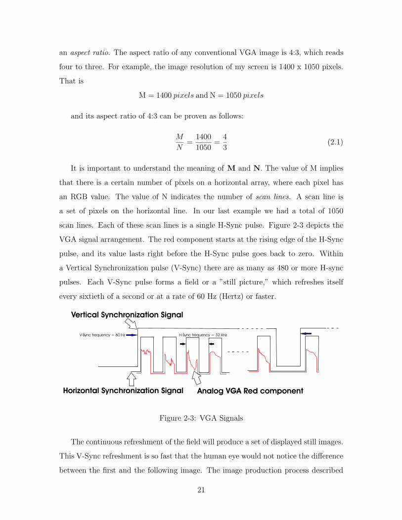
an RGB value. The value of N indicates the number of scan lines. A scan line is
a set of pixels on the horizontal line. In our last example we had a total of 1050
scan lines. Each of these scan lines is a single H-Sync pulse. Figure 2-3 depicts the
VGA signal arrangement. The red component starts at the rising edge of the H-Sync
pulse, and its value lasts right before the H-Sync pulse goes back to zero. Within
a Vertical Synchronization pulse (V-Sync) there are as many as 480 or more H-sync
pulses. Each V-Sync pulse forms a field or a ”still picture,” which refreshes itself
every sixtieth of a second or at a rate of 60 Hz (Hertz) or faster.
Vertical Synchronization Signal
Horizontal Synchronization Signal Analog VGA Red component
V-Sync frequency = 60 Hz H-Sync frequency = 32 KHz
Figure 2-3: VGA Signals
The continuous refreshment of the field will produce a set of displayed still images.
This V-Sync refreshment is so fast that the human eye would not notice the difference
between the first and the following image. The image production process described
21

above is nothing but a sequence of pictures which we call video.
Summary: Video is decomposed into five major signals which are the R, G, B,
H-Sync, and V-Sync signals. The combination of the RGB components produce color,
and the color is a function of the RGB intensities. A single H-Sync pulse at its rising
edge contain M number of pixels and each pixel contain an RGB value. A set of N
number of H-Sync pulses (referred to the V-Sync) produces a ”still image”. The rate
of every still image is of one sixtieth of a second or 60 Hz. This rate is so fast that the
human eye cannot distinguish between two different fields. The sequence of images is
what we called video.
Analog to Digital Converter (ADC)
Once we know how video behaves, now we are able to understand how VGA signals
will be treated for the MLPP. The signal to be treated in this section is the R
component. This signal comes from any VGA source. The R component passes
through an 8-bit ADC. The digitized signal is then processed by the FPGA and video
is displayed after this process.
The ADC08100 used for the MLPP is a device which receives one analog signal
which in turn is converted into an 8-bit digital word (refer to Appendix A). The
selection of this chip was based on the assumption of its small power consumption
which reduces to 1.3 mW (mili-watts) per MHz (Mega Hertz) of clock frequency. Its
clock frequency is taken from the FPGA clock which is 50 MHz, giving a top power
consumption of 65 mW. With this specification the ADC08100 can run on battery
power.
The process of digitization is depicted in Figure 2-4. As seen in the figure, the
analog signal enters the ADC as a function of time X(t). Our sampling time Ts is
selected in such a way to satisfy the Nyquist Theorem, which states that the highest
frequency of any signal which can be accurately represented is less than one-half
of the sampling rate. That means that if we chose a resolution of 640x480 pixels,
we have a total of 307,200 pixels depicted at 1/60 seconds or 16.66 ms. With this
information we can assume that each pixel takes about 16.66307,200
= 54.25 ns per pixel,
22

Table 2.1: Red scale based on the two most significant bits of the ADC08100 D7 andD6
D7 (MSB) D6 Description1 1 Laser Brightness High1 0 Laser Brightness Medium0 1 Laser Brightness Low0 0 Laser Off
which corresponds to 18.43 MHz. The FPGA clock frequency that feeds the ADC
is 50 MHz, which means that the analog signal can be represented accurately into a
digital signal X[n].
X(t)8-Bit ADC
@50MHz
Ts
X[n]
8-Bit ResolutionHigh
Med
Low
Off
2-Bit Resolution00
01
10
11
Analog VGA Signal Digital VGA Signal
Sampling Time
Figure 2-4: Digitizing VGA Signals
The resolution chosen for the MLPP is now based on two bits. The data taken from
the ADC08100 is only the two most significant bits (MSB). With this information
we will see a 2-bit displayed image. The final output will be a four red shade based
video. The criterion of this red scale is shown in Table 2-1.
2.1.2 The Software
The MLPP is designed mainly by software. The VHDL language is a powerful tool
used to program any FPGA device. The MLPP design consists of the management of
many I/O signals. The main input signals are the R component, H-sync and V-sync
signals, including the FPGA clock signal that runs at 50 MHz.
The software design is composed of many independent modules that are connected
23

in a way that combines digital design as well as software pseudo codes, which makes
it easy to debug. The basic idea is depicted in Figure 2-5. The process begins with
a data selector where all signals are processed individually. This data selector takes
the values of the red components, Red0 and Red1, Red0 being the MSB from the
ADC. Inside the data selector there is an internal counter (hcnt) directly controlled by
the CLK(clock) and the H-sync signals. Each clock cycle is counted by the internal
counter while the H-sync signal is in ”logic one,” and it stops and resets when H-sync
is in ”logic zero.”
CLK
H-Sync
V-Sync
Red-0
Red-1
MSB
Data Selector
MLPP Input Signals:3 State
Buffer
3 State
Buffer
3 State
Buffer
3 State
Buffer
T1
T2
T3
T4
Pixel 1, 5, 9...
Pixel 2, 6, 10...
Pixel 3, 7, 11...
Pixel 4, 8, 12...
Laser Actuator
State Machines
Laser 1
Laser 2
Laser 3
Laser 50
MLPP Outputs
Brushless DC
Motor Control
CLK
V-Sync
Signal Divider
2-Bit Laser Data
T1
T2
T3
T4
Digital
To
Analog
Converter
Right Shift
Piezo-electric
Signal
Memory
Figure 2-5: Software Block Diagram
The data selector will start to acquire the red component data 2 µs after the
H-sync signal sets up to logic one, in other words, after the internal clock counts up
24

to one hundred clock cycles. The FPGA needs to store each pixel’s information from
this red component signal every two clock cycles or every 4 ns. The FPGA will not
get any data in less than this time.
At this point for the MLPP design, we need to remember that our goal is to reach
a resolution of 200 pixels on the horizontal line by 150 on the vertical line. This is
following the aspect ratio of 4:3 where 200/150 = 4/3. Since we have only 50 micro
lasers, we are going to focus first on the horizontal line. The solution to the problem
is to store the red component data into a three-state buffer. A three-state buffer is
basically a place where digital data can be placed temporarily and its outputs are
”logic one,” ”logic zero,” and ”high impedance” (Z). Table 2.2 shows how data is
stored at each buffer. Each buffer stores data of every other pixel. In this case since
Table 2.2: Laser Storage for Four-Way Shifting
Buffer at Time Internal Counter Range Trigger RangeT1 100 - 492 98 - 99T2 102 - 494 415 - 416T3 104 - 496 732 - 733T4 106 - 498 1049 - 1050
we need four pixels per laser, the data selector skips every four pixels to the particular
buffer. For example, the buffer that is triggered by the signal T1 receives information
from pixel 1 and at a later time receives information from pixel 5, pixel 9 and so on.
The same happens to the remaining three other buffers.
Looking back to Figure 2-5, we observe four three-state buffers. These buffers
have almost as many inputs as outputs. They receive the red component data and
store it until the control signal Tn is triggered and enables the buffer to pass the
information to the laser actuator. Meanwhile, when a buffer is not triggered, it
remains at high impedance. A high impedance system could be compared to a system
that is disconnected in such a way that no current may flow through the wires. High
impedance is used in these buffers to avoid undesired digital information that may
interfere with one buffer or another. When all four buffers are completely loaded,
25

a horizontal scan line has been accomplished. When the next scan line begins the
buffers will acquire their information right after they send the previous data to the
laser actuator. The process keeps going until it reaches the last horizontal scan line.
Remember from Table 2.2 that the first set of data is triggered when T1 is at logic
one, two clock cycles before we begin to acquire the next scan line information. This
means that the projected display is only one scan line delayed from the VGA source
image.
The laser actuator is a module that receives buffer information at the time Tn.
This actuator is a set of state machines that are controlled by an internal counter,
similar to the data selector counter. A state machine is a decision-making module
that depends directly on a specific input, and the number of decisions is directly
proportional to 2n, where n is the number of bits. For example, if we have a two bit
statement or input, the only options we will have as an input are: ”00”, ”01”, ”10”,
and ”11” (i.e. only 22 = 4 options). In our particular case, these are the values of
the red component that are stored on the three-state buffers. Each state machine will
receive only one of the past options and will determine what to do with the received
information. For example, if the input is a ”11”,which is brightness HIGH (from
Table 2.1), then the state machine will ”decide” for the designated laser to stay on
for 314 clock cycles or 6.28 µs. This is the most time that the laser stays on. When
the input is a ”10”, brightness MEDIUM, the state machine will light up the laser
for 157 clock cycles or 3.14 µs. Finally, if the actuator receives a ”01”, brightness
LOW”, the laser will be on for only 79 clock cycles or 1.58 µs. However, if the data
received is a ”00”, laser OFF, the laser will remain off at least the 314 clock cycles.
To better understand Table 2.2, we will summarize the process. After all the
buffers are completely loaded, the system is waiting for the trigger signals, which are:
T1, T2, T3, and T4. The buffer triggered by T1 starts storing data when the clock
cycle equals one hundred. This buffer will get data from the data selector every eight
clock cycles, since we need to skip four pixels and each pixel takes two clock cycles
to be acquired by the buffer. The following equation explains the behavior of the
26

internal counter hcnt:
hcnt = 100 + 8 ∗ 49 = 492 (2.2)
This equation helps us to determine the lower and upper bound for the first 50 skipped
pixels which are from pixel 1, pixel 5, pixel 9, all the way to pixel 197. The rest of
the table follows the same equation but starting from 102 for buffer T2, 104 for buffer
T3, and 106 for buffer T4, which ends on pixel 200. The trigger range for buffer T1
starts on clock cycle 98 and lasts only two clock cycles for accessing the laser actuator.
After 314 clock cycles, the buffer T2 is triggered at clock cycle 415 instead of clock
cycle 413, giving only two more cycles to avoid any glitches. The same process is
repeated for buffers T3 and T4.
Piezo Electric Actuator
As shown in Figure 2-5, there is a module which has as inputs T1, T2, T3, and T4
signals. These signals go to a submodule, not depicted in the figure that is a memory
that retains the Tn information. The module’s outputs go to an external digital to
analog converter (DAC), which is a small ladder resistor array. This DAC produces
a ladder like signal. This signal is very important in order to drive the piezo-electric
device to make the right to left jitter.
Brushless DC Motor Actuator
Finally, the last module depicted in Figure 2-5 is the DC Brushless Motor Actuator.
This actuator has an internal counter ”vcnt” that is governed by the FPGA clock
signal (CLK) and the V-Sync signal. As depicted on Figure 2-3 the V-Sync signal
is not uniform, in other words, is not 50% duty cycle. Instead it is 96% duty cycle,
which means that 96% of the signal periodic time stays on logic one, and the rest is on
logic zero. The brushless motor actuator is nothing but a compensator. For example,
the signal at 96% duty cycle is transformed to a signal at 50% duty cycle. This signal
is critical to synchronize the prism’s faces attached to the brushless motor, in order
to project the display without wiggling.
27
2.2 VCSEL Technology and Fabrication
The acronym VCSEL stands for Vertical Cavity Surface Emitting LASER and con-
tains itself another acronym, which is LASER. This word stands for Light Amplification
through Stimulated Emission of Radiation. To better understand this concept we
must start by explaining some basics. First, let us start with the concept of light
generation. Consider any particular metal, and no matter which one we pick it has
atoms. Next, we concentrate on one atom and analyze its structure. As we may
know, atoms are composed of neutrons, protons, and electrons. The electrons nor-
mally travel within an orbit around the nucleus, which is composed of neutrons and
protons. When the electrons travel in their own orbit we might say that the atom is
in ground state [13]. Supposing that energy is applied to this atom (e.g., thermal or
electrical excitation), and this energy is strong enough to move one or more electrons
to a ”higher” orbit or energy level, then we may say that the atom is in the exited
state. After this phenomenon and naturally, this electron will return to its equilib-
rium or its original orbit; in other words, the atom goes from the exited to ground
state. This action will constitute a photon liberation. Light is composed of photons,
so the process described above will be is light generation.
Light amplification is the next thing to consider for lasers. Consider a third-level
system that consists of a ground state, an exited state, and a super-excited state. To
begin with the example, let us say that a set of atoms in the system are at ground
state, and after some type of excitation most of the atoms go from ground to the
excited state. The super-excited state is utilized as a short-lived ”pivot point.” When
a photon enters into the system it ”knocks” an electron from the excited state down to
ground state, thus creating a new photon. Two photons will leave the system instead
of one. After these photons leave the system, they are reflected by a mirror sending
these two photons back to the system. At this moment, they enter the system and
another two atoms get knocked down from the excited to ground state. This time
there will be four photons leaving the system in the opposite direction and that are
then reflected by a second mirror. This amplification process is called stimulated
28
emission.
A laser is composed of three main things: a gain medium (e.g., third-level sys-
tem), a fully reflecting mirror, and a partially reflecting mirror. With all these three
elements we can consider this as a positive feedback system. Laser light is then cre-
ated by the following procedure; an external force like electricity, excites the atoms
within the gain medium, and a photon enters the gain medium. As an output we will
see more photons and they will be bounced back by the partially reflecting mirror.
Then, these photons re-enter the system and light gets amplified again. As an output
we will see even more photons exiting in the opposite direction and getting bounced
back by the fully reflecting mirror, forcing to re-enter the system so light is amplified
again. When the light is strong enough, it penetrates the partially reflecting mirror
and we get what is called a coherent light.
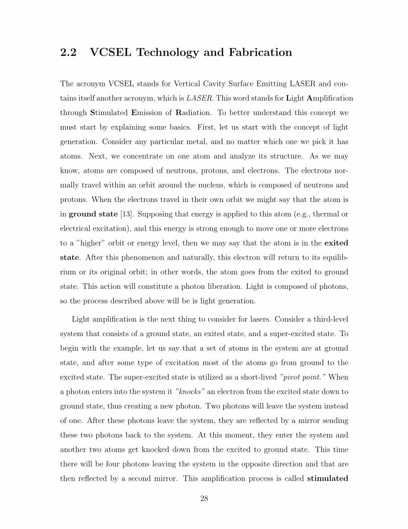
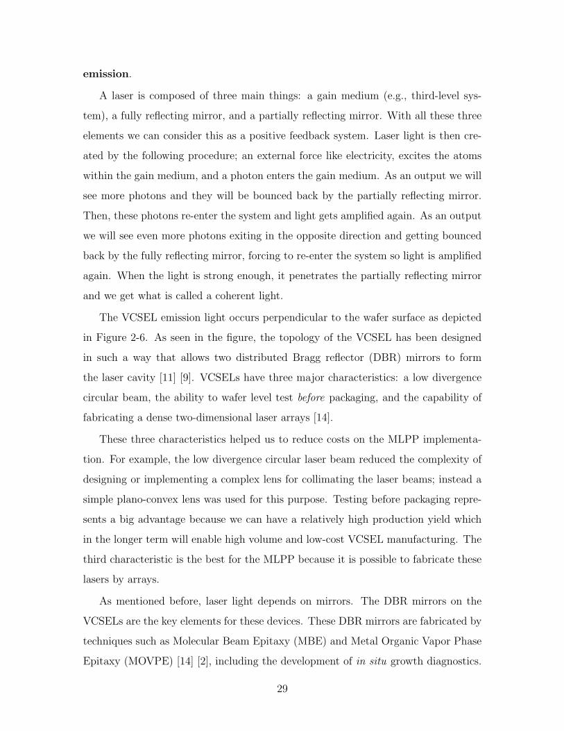
The VCSEL emission light occurs perpendicular to the wafer surface as depicted
in Figure 2-6. As seen in the figure, the topology of the VCSEL has been designed
in such a way that allows two distributed Bragg reflector (DBR) mirrors to form
the laser cavity [11] [9]. VCSELs have three major characteristics: a low divergence
circular beam, the ability to wafer level test before packaging, and the capability of
fabricating a dense two-dimensional laser arrays [14].
These three characteristics helped us to reduce costs on the MLPP implementa-
tion. For example, the low divergence circular laser beam reduced the complexity of
designing or implementing a complex lens for collimating the laser beams; instead a
simple plano-convex lens was used for this purpose. Testing before packaging repre-
sents a big advantage because we can have a relatively high production yield which
in the longer term will enable high volume and low-cost VCSEL manufacturing. The
third characteristic is the best for the MLPP because it is possible to fabricate these
lasers by arrays.
As mentioned before, laser light depends on mirrors. The DBR mirrors on the
VCSELs are the key elements for these devices. These DBR mirrors are fabricated by
techniques such as Molecular Beam Epitaxy (MBE) and Metal Organic Vapor Phase
Epitaxy (MOVPE) [14] [2], including the development of in situ growth diagnostics.
29

Optical Output
Metal ContactP-Mirror StackProton ImplantActive RegionLaser CavityN-Mirror StackGaAs SubstrateMetal Contact
Figure 2-6: VCSEL Cross Section
These DBR mirrors are separated by a thickness of a multiple of λ/2 where λ is the
wavelength of the emitted light [8]. The distance between the top and the bottom
mirror stacks is called the optical cavity which is typically one wavelength long where
we find the active laser region. These mirrors are designed in such a way so as to be
almost 99% reflective. Monolithic semiconductor DBR mirrors have a lower index of
contrast and thus require a higher number of mirror periods for high reflectivity [12].
As we can see from Figure 2-6, DBR mirrors come in stacks of which each layer is
called a period. The higher the period, the more reflective it becomes. Notice that
on the top of the VCSEL we have fewer mirror stacks than in the bottom [20]. The
bottom layers have to be more reflective than the top so the light can ”escape” on
the top. The composition of the layers is chosen to maximize the index of contrast
and to be transparent to the laser light [18]. For example, if we want a 850 nm or 650
nm wavelength laser we can use pairs of Al0.2Ga0.8As/AlAs or Al0.5Ga0.5As/AlAs
respectively.
The VCSEL technology is mainly used for telecommunication purposes as well
as for proximity sensors, encoders, laser range finders, laser printing, bar coders,
and optical storage among others. Because of the nature of the typical VCSEL
30
applications, they are commonly fabricated for wavelengths above 690 nm. This
wavelength is barely visible to human eyes, since the range of eye sensitivity goes from
440 nm to 690 nm approximately [17]. Some VCSEL prototypes have been developed
for wavelengths shorter than 690 nm, like the MLPP, almost on the infrared region.
Laser image displaying has not been considered before, and the development of ideal
VCSELs in wavelengths such as 440 nm (Blue range), 555 nm (Green range) and 625
nm (Red range) are now in research. In the near future VCSELs developed on the
RGB range will help us to display a full color laser projection display.
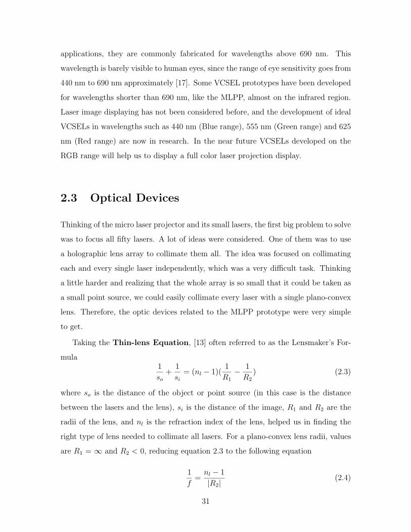
2.3 Optical Devices
Thinking of the micro laser projector and its small lasers, the first big problem to solve
was to focus all fifty lasers. A lot of ideas were considered. One of them was to use
a holographic lens array to collimate them all. The idea was focused on collimating
each and every single laser independently, which was a very difficult task. Thinking
a little harder and realizing that the whole array is so small that it could be taken as
a small point source, we could easily collimate every laser with a single plano-convex
lens. Therefore, the optic devices related to the MLPP prototype were very simple
to get.
Taking the Thin-lens Equation, [13] often referred to as the Lensmaker’s For-
mula1
so
+1
si
= (nl − 1)(1
R1
− 1
R2
) (2.3)
where so is the distance of the object or point source (in this case is the distance
between the lasers and the lens), si is the distance of the image, R1 and R2 are the
radii of the lens, and nl is the refraction index of the lens, helped us in finding the
right type of lens needed to collimate all lasers. For a plano-convex lens radii, values
are R1 = ∞ and R2 < 0, reducing equation 2.3 to the following equation
1
f=
nl − 1
|R2| (2.4)
31

where f is the focal point of the lens. Starting from the fact that our lasers were
taken as a spherical wave point source which can be represented as
a(x, y, z, t) = Aej(kR−ωt)
jR(2.5)
and we suppose the paraxial approximation (refer to Figure 2-7), a very short distance
approximation. We end up with the following math expression for our point source
which is
a(x, y, z) = Aej2π zλ+jπ x2+y2
λz (2.6)
where k = 2πλ
is the wave number where this time λ is the period of each outgoing
wavefront.
RPoint
Source
Outgoing
Parabolic
WavefrontsOutgoing
Rays
Figure 2-7: Spherical Wave in the paraxial approximation
The role of any thin lens is to transform a spherical wavefront into a plane wave
and vice-versa. The problem now, is that when our point source (the lasers) is at
the exact focal point f, we will produce an image of the size of the diameter of the
lens. To avoid this inconvenience, it was necessary to move the focal point a little bit
farther away such as f ′ = f + ∆f , in other words, to de-focus the system a little bit.
This action yielded an output divergence where the final image increased its size until
we had the desired image size of one meter diagonal long. Some of the trade offs that
we deal with when de-focusing the system was that our image blurred. This could
be inconvenient, but fortunately was not, because blurring the image (not too much)
helped to cover the inherent 100 µm pitch gaps that the VCSELs have. Although,
these gaps were not covered at 100%. Another special technique is going to be applied
to enhance the image resolution. This technique is described in section 2.4, where
32

piezo-electric devices will be used.
A previous MLPP prototype used a galvanometer for beam steering. It consisted
in a single mirror attached to the galvanometer. This mirror was deflected by some
degrees and then move back to the original position. The problem with this prototype
was that the energy used to move the galvanometer was too much. For example, to
move the mirror one degree, we needed 50 mA. Moving the mirror 24 degrees, would
take about 1.2 A, which is considered too much current to drive. Another issue was
that the galvanometer is very heavy and very big. A brushless or a stepper motor was
considered as an alternate solution to the beam steering problem, including power
consumption.
The other optic device used for the MLPP was a rotating mirror. This mirror
must have certain characteristics so it can display video at a rate of 60 Hz. The first
step was to choose a shape. The shape that was convenient for the application is a
polygon. The first thing was to calculate the number of facets. The formula for the
number of facets is given by [5]:
n =720(C)
θ(2.7)
where θ is the active optical scan angle and C is the duty cycle. The number must
be an integer, if not, then there is no exact solution for the system. In our case,
we previously decided a duty cycle of 50% (section 2.1.2), and a 60o displayed angle,
giving a total of 720(0.5)60o = 6 facets. The second step was to decide the size of each
facet. We already know that the width has to be at least 15 mm long, because both
laser arrays measure 12 mm long. The length of the facets must be calculated from
[5]:
L(mm) =(D′ + 1)
1− C(2.8)
where D′ is the laser spot width, which experimentally measure approximately 0.2
mm, where the laser path is the two VCSEL arrays that measure all together phys-
ically from laser #1 to laser #50 10 mm . Our hexagon length must be equal to or
greater than L(mm) = D′+11−C
= 0.2+11−0.5
= 2.4mm. Some experiments were done while de-
33

signing gold plated hexagons. The results of these experiments showed that the bigger
the facet length the bigger the displayed image. For experimental purposes, the size
of the polygon facets are 12 mm each. In theory a 6 mm facet can be implemented.
2.4 Piezo-Electric Devices
Most piezos are made of polycrystalline oxide ceramic PZT. The letters PZT stand for
lead (Pb), zirconium (Zi), and titanium (Ti), which are the basic components of most
piezo devices. Basically, any piezo-electric device of any material reacts when applying
a voltage to it. This kind of reaction is expressed into internal displacement or
deformation. This reaction can be reversed and we might obtain voltage by deforming
or pressing the piezo-device. Some commercial piezo-electric devices come in stacks.
These stacks are often used to increase the displacement of the device, but the increase
of displacement, even with the increase of stacks, will reduce the resonant frequency
of the piezo devices.
The MLPP has a resolution of 50 x 480 pixels in its recent prototype. To increase
its image resolution it is convenient to think in new ways of increasing the number of
pixels. Fortunately the software provides the laser driver to make each laser display
four different pixels. Nevertheless, a physical actuator has to be implemented to
”move” the lasers from left to right four positions. An alternative to do this task is
the use of piezo-electric devices.
Recalling from section 2.1.1 Figure 2-3 the H-sync signal has a frequency of ap-
proximately 32 KHz, and so the right shift piezo-electric signal (RSPES). The idea
is to apply the RSPES to a specific piezo-electric device to make a right shifting of
a plano-convex lens. This action will give us the effect of ”moving” the lasers from
left to right four positions. The desired displacement for each shift is about 10 µm
since the diameter of each laser is about that size. The total desired displacement is
30 µm at 32 KHz. Unfortunately there is no actual piezo-actuator that can give us
this characteristics of moving at least 30 µm with a resonant frequency of 30 KHz or
higher [3] [1].
34

Chapter 3
Implementation
This chapter will describe how the MLPP has been implemented, including circuit
and board designs as well as micro technology techniques. Some circuit designs and
considerations on building micro-boards for the VCSELs will be described on this
chapter.
3.1 Mini Board Design and Implementation
Before bonding lasers at size of 10µm of diameter with a pitch of 100 µm from one laser
path to the other, a mini board has to be designed. Implementation of the ceramic
board requires training at the Microsystems Technology Laboratories (MTL). The
design is depicted in Figure 3-1. The board dimensions were designed in such a way
Wilfrido SierraMIT Media LabApril 2003MLPP v 2.0
L1L2L3L4L5L6
L7
L8
L9
L10
L11
L12
L13
L14
L15
L16
L17
L18
L19
L20 L21 L22 L23 L24 L25 L26 L27 L28 L30 L31L29 L32
L33
L34
L35
L36
L37
L38
L39
L40
L41
L42
L43
L44
L45L46L47L48L49L50GND NC
Figure 3-1: Laser Board Photo Mask (Actual Size)
that it must fit into another 1in x 1in board, which is a very common technique when
a design this small has to be implemented into a ”normal” size board. The mini
35

board is a ceramic made board with gold coating. The technique applied for this
mini board is called the ”liftoff” technique. It consists of the following procedures:
1 First we take a blank ceramic board. For best results, this board has to be immersed
in acid called piranha, which is a 4:1 composition of sulfuric acid (H2SO4) and
hydrogen peroxide (H2O2). This process cleans all impurities that it might
have so the following steps can be successful. Failure to a previous cleaning
with ”piranha” may cause future damage to the board design.
2 After carefully cleaning the board, we rinse the board, and blow dry with dry air.
Then the board goes to the ”Hard Bake” oven. This oven is around 120 to 130o
C. We let it bake for 20 to 30 minutes.
3 Once the sample is ready, we take it out from the hard bake oven and begin with
the small vacuum chamber, where we deposit the board and a small quantity of
HDMS on a small cup on its side. This substance is nothing but a ”primer” for
the photoresist that will be poured afterwards. This primer is used so the surface
of the board smoothes up, letting any type of liquid to attach uniformly on the
board surface. We wait 10 minutes until the HDMS evaporates completely.
At this point we take the sample into the spinner. We must have ready the
photoresist AZ 5214-E. The photoresist is a layer which in the future we will
use to make the liftoff. On the spinner, we control the RPM (Revolutions Per
Minute) for two main purposes: the first is to pour the photoresist on the
sample at a slow rate so it uniformly covers the board in order to avoid ”gaps”
or unfilled areas among the ceramic board; the second is to increase the speed
(at 2500 RPM) to let it dry.
4 Now that the sample is uniformly covered by the AZ 5214-E photoresist, we take
it to the ”soft bake” oven (at 90o C) for about twenty minutes. This procedure
is just to let it dry, but we must be careful not to exceed this time, otherwise
the Az 5214-E will harden and will make it almost impossible to accomplish
further steps.
36
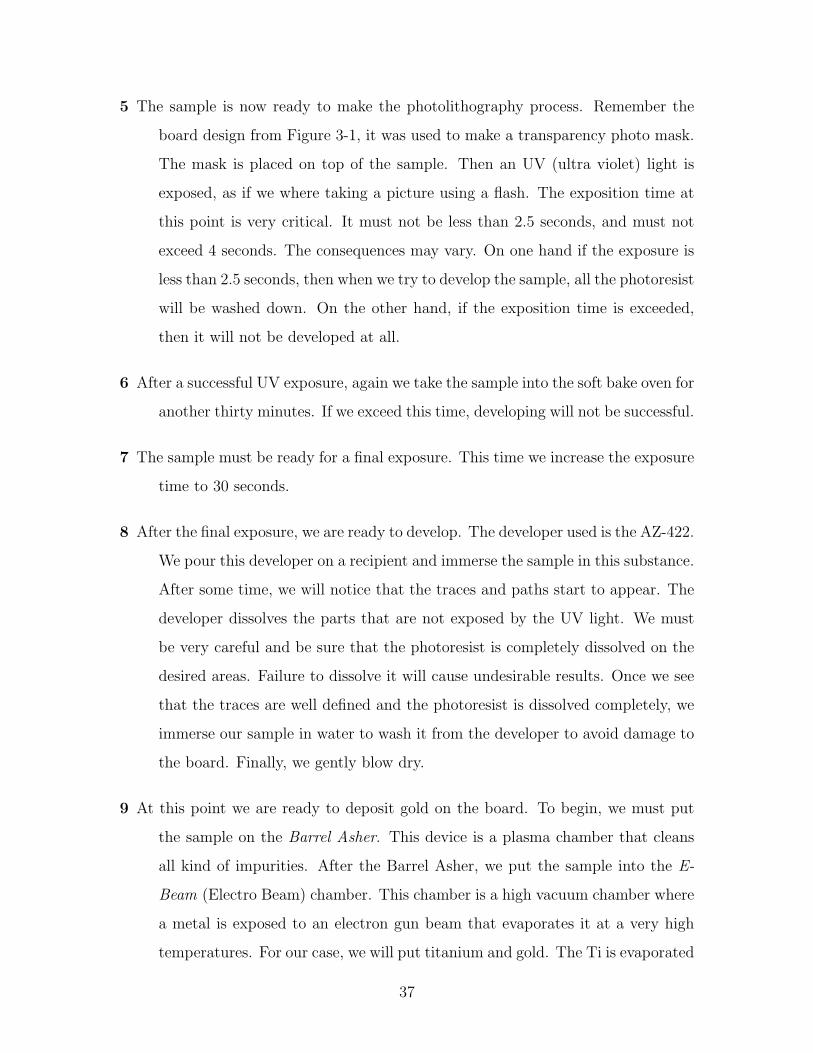
5 The sample is now ready to make the photolithography process. Remember the
board design from Figure 3-1, it was used to make a transparency photo mask.
The mask is placed on top of the sample. Then an UV (ultra violet) light is
exposed, as if we where taking a picture using a flash. The exposition time at
this point is very critical. It must not be less than 2.5 seconds, and must not
exceed 4 seconds. The consequences may vary. On one hand if the exposure is
less than 2.5 seconds, then when we try to develop the sample, all the photoresist
will be washed down. On the other hand, if the exposition time is exceeded,
then it will not be developed at all.
6 After a successful UV exposure, again we take the sample into the soft bake oven for
another thirty minutes. If we exceed this time, developing will not be successful.
7 The sample must be ready for a final exposure. This time we increase the exposure
time to 30 seconds.
8 After the final exposure, we are ready to develop. The developer used is the AZ-422.
We pour this developer on a recipient and immerse the sample in this substance.
After some time, we will notice that the traces and paths start to appear. The
developer dissolves the parts that are not exposed by the UV light. We must
be very careful and be sure that the photoresist is completely dissolved on the
desired areas. Failure to dissolve it will cause undesirable results. Once we see
that the traces are well defined and the photoresist is dissolved completely, we
immerse our sample in water to wash it from the developer to avoid damage to
the board. Finally, we gently blow dry.
9 At this point we are ready to deposit gold on the board. To begin, we must put
the sample on the Barrel Asher. This device is a plasma chamber that cleans
all kind of impurities. After the Barrel Asher, we put the sample into the E-
Beam (Electro Beam) chamber. This chamber is a high vacuum chamber where
a metal is exposed to an electron gun beam that evaporates it at a very high
temperatures. For our case, we will put titanium and gold. The Ti is evaporated
37

and its vapors will be poured on our sample. The desired deposition thickness
is around 50 A(Angstroms), so it will attach well to the ceramic board. For gold
deposition it is desirable to have around 500 A to 700 A deposition thickness,
so the inherent resistivity is not too big and avoid in-board heating when the
lasers are all turned on.
10 Finally, after a successful Ti and Au deposition, we put our sample into acetone
to remove the photoresist from the ceramic board. The final result is a board
with gold traces, as depicted in Figure 3-2., ready to be bonded by the gold
wire bonder.
Figure 3-2: Ceramic Laser Board
3.1.1 Wire Bonding
Another difficulty is to bond the fifty lasers into the ceramic board. As it seems,
wire bonding is not an easy task. Previous knowledge of wire bonding is required.
Before starting to bond, the two dice are glued with silver epoxy and we let dry for a
few hours. A recommendation is to use isopropyl to clean the lasers before bonding.
Patience is the key to bond the lasers to the ceramic board. Figure 3-3 shows one
laser die ready to be bonded. The capillary is positioned on top of the VCSEL array
38

over the gold pads. Moving the capillary is like moving a computer mouse, which has
one button that is used to trigger the capillary from top to bottom.
Wire Clamp
Capillary
Gold Ball
VCSEL Die
Figure 3-3: Gold Ball Bonder and a VCSEL Die
Figure 3-4 depicts the sequence of how the gold wire bonder works. Figure 3-
4 A shows how the capillary hits the VCSEL’s gold pad using ultrasonic vibration
to make a good gold-to-gold bonding. The clamps are open at this moment so the
gold wire moves freely down. After a successful gold-to-gold bonding, the capillary
moves upright to the loop position height predetermined by a knob located on the
wire bonder device. Then the capillary is moved towards the mini board gold pad as
shown on Figure 3-4 B. When the capillary is in the right position the mouse button
is triggered again and a wedge bonding is done using an ultrasonic vibration to bond
the wire to the mini board as depicted in Figure 3-4 C and D. Finally, the clamps
are closed when the capillary moves upright again, so the the gold wire stays down
in the right position. A spark hits the tip of the wire to form a gold ball again ready
to make the next bond. Figure 3-5 shows a real gold and wedge bonding.
3.2 Hardware Implementation
After wire bonding the lasers, an encapsulated device was fabricated to avoid dust
and other impurities that may land on the device. A picture of the encapsulated
device is depicted in Figure 3-6. On top of the protection device lies a plano-convex
lens that focuses the laser beams. Above the lens, a prism mirror is attached to a
39

A) B) C)
D) E) F)
VCSEL Die
Gold Pad
Electronic Spark
Ball Bond
Wedge Bond
The Capillary hits the VCSEL Die
deforming the gold ball, ultrasound
vibration is then applied.
After the ball is bonded to the
die, the capillary rises to the loop
height position.
Then the capillary hits
the gold pad while the
clamps remain open.
The capillary deforms the
gold wire, producing a
wedge, after an applied
ultrasonic vibration. The clamps
are closed by this time.
When the capillary rises,
an electronic spark is applied
to the gold wire to form again
a gold ball, ready for the next
bond.
The gold ball is formed at
this time.
Figure 3-4: Bonding Sequence
Figure 3-5: Gold Ball and Wedge bonding respectively [16]
brushless motor. This motor is the beam actuator that deflects the lasers in a vertical
way. This steering subsystem is connected directly to the FPGA board. The internal
FPGA design can be seen in Appendix A.
A large variety of mirrors were designed, from cover glass or acrylic, in different
sizes. Both materials were gold coated on the E-Beam chamber with a variety of
40

Figure 3-6: Laser Protection mounted over the board
gold thickness deposition in order to find the best reflective index, that allows the
laser to be 99.9% reflected. The recommended thickness to get this reflective index is
approximately 920 A. A higher deposition may cause damage on the acrylic, burning
it down and losing its mirror properties. As for the cover glass, a thicker deposition
may cause blurriness on the sample, completely ruining its mirror properties. The
deposition rate is also important. Making a deposition at a rate equal to or lesser
than 1 A/s is strongly recommended. A higher deposition rate will require more
energy and therefore a higher temperature inside the vacuum chamber.
Many lens sizes were implemented to verify the most convenient type of plano-
convex lens. The type of lenses selected are shown in Table 3.1. After trying many
focal lengths and lens sizes, the most convenient lens to use was the 15 mm diameter
lens because it focuses all lasers with the desired divergence, and also because it is
at the limit of collimating these lasers. The 18 mm and 20 mm lenses could be used,
but they occupy most of the space on the prototype. After the 15 mm lens selection,
the next step was to cut this lens into three equal portions to reduce space, so the
middle part was the only part used to collimate all the lasers (see Figure 3-7).
41

Figure 3-7: Implemented Lens
Table 3.1: Lens Dimension Options
Lens Diameter (mm) Lens Focal Length (mm)12 1215 1518 1820 20
3.3 Results
The MLPP is displaying a video image with a resolution of 50x480 pixels. The
implementation of a piezo-electric device is still under research. At the moment there
is no piezo-electric device that can actually give at least 40 µm displacement at a
resonant frequency of 32 KHz. New ways of solving this issue have been taken into
consideration. One possible solution is to reduce the number of horizontal scan lines
so we can reduce the horizontal frequency, in order to reach a resonant frequency from
approximately 12 to 15 KHz. At this frequency there are many piezos that produce a
displacement of 40 µm with a force of at least 5 N (Newtons), enough to move a glass
lens from left to right. Another way to solve the problem is to implement a 4 sided
mirror polygon spinning at a rate of approximately 32 KHz, where each of its sides
has a degree of deflection different from the other. With these deflections it might
be possible to achieve four different displacements from left to right, to increase the
image resolution. One last solution is to build a denser VCSEL array so the gaps
42

between each laser are barely noticed. A problem with this will occur since VCSEL
robustness is evidenced by maximum continuous wave lasing temperature T = 2000
C [19]. This means that VCSELs produce heat, and the more current they drive, the
more heat they dissipate and vice-versa. Since its robustness is a function of heat,
the closer the lasers on the VCSELs are placed against each other, the more heat is
going to be transferred on each laser cavity. This information proves that the closer
they get, the less current they have to drive and therefore the less energy we need to
drive them, and the dimmer the image we get. Figure 3-8 depicts the laser images
displayed by the MLPP. At the middle of the picture appears a black line. This black
line is a gap that each VCSEL die has inherently. When gluing both VCSEL dies
together, there is a gap of approximately 440 µm, equivalent to 4 laser spots. We
can overcome this problem by either getting a straight 50 laser array instead of two
arrays of 25 lasers each, or to die saw both 25 array VCSELs. The second option is
too risky and so it was not considered.
A) Original Image B) Projected Image
Figure 3-8: Displayed Laser Image
The laser images are not bright enough at day light illumination due to the wave-
43

length of 670 nm. The brightness will increase in a non-linear way as the wavelength
decreases up to 555 nm. Meanwhile, in a not too dark spot, a remarkable image is
seen. Unfortunately present technology can not support brighter VCSELs because
their applications are not as common as those in communication business. At the
moment, blue VCSELs are being developed for high quality image processing as in
printers and DVD devices.
3.3.1 Evaluation
The MLPP prototype gives the final resolution of 50 x 480 pixels. However, the
expected resolution of 200 x 480 pixels has not been implemented yet. The signal
driver that controls the piezo-electric device is giving the correct signal output. This
signal can be amplified and implemented directly to the piezo-electric device that
makes the shifting to the right.
At this moment, the MLPP still a prototype that can be enhanced in many ways.
So far, with the software control and the proof that it is possible to display video
out of 50 micro lasers, the FPGA system can be shrunk into an ASIC (Application
Specific Integrated Circuits) where this ASIC could be as small as 1 cm x 1cm. A
relatively small brushless DC motor can be used, where a small mirror prism could be
attached to it. The smaller the motor, the less current it will use. It can be estimated
that this motor could use less than 20 mA, which is the actual current that the DC
motor uses on the prototype. The plano-convex lens has dimensions of 15 mm x 7
mm x 5 mm.
44

Chapter 4
Future Work and Applications
The MLPP development grows as a function of technological innovations such as
the development of green and blue VCSELs. However, this inconvenience will not
stop the relevance of displaying laser images, since the technical process is almost
straight forward when trying to upgrade the MLPP from monochromatic to full color
video. Implementing the RGB VCSELs could be a problem when trying to align
them. We might find that each VCSEL die will be independent and most likely we
will not find a red and blue, a green and blue, or any possible combination of VCSEL
colors on the same wafer. Fortunately, the freedom of having each RGB VCSEL
arrays as an independent die will let us overcome with the problem, which is the
chromatic aberration due to the different refraction index that the red, green and
blue wavelengths have when passing from air through a glass or acrylic lens. Figure
4-1 A depicts an axial chromatic aberration (A·CA) for a plano-convex lens. As seen
on the figure, when RGB light enters the lens, the RGB lasers demonstrate their
different refraction index and therefore they have different focal points denoted as
FB, FG, FR [13].
It is not easy to figure out the RGB VCSEL alignment since the focal points well
as the deflection angle are different. A possible solution is to use a prism which will
combine the three colors and transform them into a single RGB beam as depicted
in Figure 4-1 B. After the light is combined, a thin achromatic doublet may be used
to collimate all lasers. An achromatic doublet design should be done following some
45
H1 H2
FB FG FR
Axial Chromatic Aberration
Red
BlueYellow
Achromatic Doublet
A)
Red Laser
Green Laser
RGB Laser
Prism
B) Light Combiner
C)
Blue LaserGreen Laser Red Laser
RGB Light
RGB Light
RGB Light
RGB Light
Blue Laser
F
Figure 4-1: Chromatic Aberration
optic equations where the doublet can be considered as a positive and a negative lens
separated by a distance d having a compound focal point f
1
f=
1
f1
+1
f2
− d
f1f2
(4.1)
Referring to equation 2.3 and considering that
1
so
+1
s1
=1
f(4.2)
46

we can re-arrange equation 2.3 and 4.2 to get 1f1
= (n1 − 1)ρ1 and 1f2
= (n2 − 1)ρ2
following the idea, we can write the following equation
1
f= (n1 − 1)ρ1 + (n2 − 1)ρ2 − d(n1 − 1)ρ1(n2 − 1)ρ2 (4.3)
This final equation describes the focal point of the doublet, and since FR and FB are
the extreme focal points of the system, we want them to be equal such that 1fR
= 1fB
and using equation 4.3
(n1R−1)ρ1+(n2R−1)ρ2−d(n1R−1)ρ1(n2R−1)ρ2 = (n1B−1)ρ1+(n2B−1)ρ2−d(n1B−1)ρ1(n2B−1)ρ2
(4.4)
Suppose that the distance d = 0, where the two lenses are in contact. The expression
reduces toρ1
ρ2
= −n2B − n2R
n1B − n1R
(4.5)
The focal length of the compound lens [13] fY can be specified as that associated
with yellow light. For the component lenses in yellow light, 1f1Y
= (n1Y − 1)ρ1 and
1f2Y
= (n2Y − 1)ρ2 . Hence
ρ1
ρ2
=(n2Y − 1)f2Y
(n1Y − 1)f1Y
(4.6)
Equating 4.5 and 4.6 we get
f2Y
f1Y
= −(n2B − n2R)/(n2Y − 1)
(n1B − n1R)/(n1Y − 1)(4.7)
where the quantities (n2B−n2R)/(n2Y −1) and (n1B−n1R)/(n1Y −1) are known as the
dispersive powers of the two materials forming the lenses and their reciprocals are
known as the Abbe numbers. With these numbers we are able to look up a table
that specifies the correct material for the achromatic doublets. For more information
about doublet design please refer to Section 6.3.2 of [13].
The idea of having a full color display is more likely to gain more acceptance from
the general consumer rather than a monochromatic display. Therefore the first thing
to do is to develop an 8-bit resolution laser projector, increasing the image fidelity
47

and quality. With this upgrade, people from around the world will be able to use
the laser projector as part of their normal lives, because not only images but also
e-mail messages and any kind of text formats will be displayed. For example, the
resolution needed to display Japanese or Chinese characters, to avoid unnecessary
misunderstandings, is higher than displaying a text written in English.
The MLPP is a versatile device that has a whole variety of applications and
future developments. Venture applications could be applied in medicine where, in
a configuration of two MLPPs with perpendicular beams impinging into an active
plastic material, the Magnetic Resonance Imaging (MRI) could be displayed in a
three-dimensional way. If a 3-D laser projector is created, then many research areas
could be explored, from medicine, architecture and entertainment to aeronautical
modelling.
The MLPP can be considered as an input device. Using the time of flight tech-
nology, the MLPP can be used as a 3-D scanner. With the same technology, the
MLPP can perform keystone auto correction. Taking advantage of the laser sensor,
the surface where the video is projected (i.e., the wall, the floor, or a table) can be
used as a touch screen display.
It is important to remember that the goal for the MLPP is low power consumption,
low cost, and a size small enough to make it portable and run on batteries. With
these characteristics, it someday may substitute for the Liquid Crystal Displays of
the lap-tops and PDA’s. The MLPP is not far for a future implementation for a
hand-held device, where it can gain a final size of 2 cm x 2cm x 2cm. If the MLPP
gets market acceptance, VCSELs will become very cheap. The series production of
MLPP will make all of its components even cheaper making an total estimate of 20 to
50 USD. Eye safety is one of the most important things to consider in all applications
described before. Safety circuitry has to be designed to avoid direct eye contact. This
last feature will make the MLPP a reliable device which no one wants to live without
it, with a broad acceptance on the market.
48

Appendix A
Hardware Specification Data
Sheets
A.0.2 Analog to Digital Converter Data Sheet
ADC DATA SHEET can be found on the National web site at
http : //www.national.com/pf/AD/ADC08100.html
A.0.3 FPGA Board Description
The FPGA board design can be found at the following Digilent web site
http : //www.digilentinc.com/Catalog/digilab 2e.html
49

50

Appendix B
Software Source
The following sections will describe the code source for the MLPP. Note that the
subindexes are shifted. At a similar fashion the names were changed. Here in this
appendix the name of the modules are as they appear originally on the FPGA.
B.0.4 Main Driver 0
The original name of this submodule is ”mainT0 sch”. The code is shown below:
library IEEE;
use IEEE.STD LOGIC 1164.ALL;
use IEEE.STD LOGIC ARITH.ALL;
use IEEE.STD LOGIC UNSIGNED.ALL;
–This is the main driver that controls all 50 lasers.
At time T0, pixels p1, p5, p9, p13, p17 etc... are lit at this
time. Buffer T0 will gather all the information for these pixels
entity mainT0 sch is
Port (
contador : in std ulogic; –internal counter
rst : in std ulogic; –async reset input
hsyncin : in std ulogic; –horizontal sync input
vsyncin : in std ulogic; –vertical sync input
51

rin0 : in std ulogic; –MSB for Red input
rin1 : in std ulogic; –LSB for Red input (out of 2 bits)
red0, red1, red2, red3, red4, red5, red6, red7,
red8, red9, red10, red11, red12, red13, red14,
red15, red16, red17, red18, red19, red20, red21,
red22, red23, red24, red25, red26, red27, red28,
red29, red30, red31, red32, red33, red34, red35,
red36, red37, red38, red39, red40, red41, red42,
red43, red44, red45, red46, red47, red48, red49,
red50, red51, red52, red53, red54, red55, red56,
red57, red58, red59, red60, red61, red62, red63,
red64, red65, red66, red67, red68, red69, red70,
red71, red72, red73, red74, red75, red76, red77,
red78, red79, red80, red81, red82, red83, red84,
red85, red86, red87, red88, red89, red90, red91,
red92, red93, red94, red95, red96, red97, red98,
red99 : out std ulogic; –all red outputs (50)
BE : out std ulogic; –enables all buffers
SME : out std ulogic; –enables State Machines
rout0, rout1 : out std ulogic; –vga red components
hsyncout : out std ulogic; –horizontal sync output
vsyncout : out std ulogic
);
end mainT0 sch;
architecture Behavioral of mainT0 sch is –Internal Signal
Declaration**************************************************
signal hcnt: std logic vector(10 downto 0);
************************************************************
begin
–Passtrhough
52

Signals********************************************************
hsyncout <= hsyncin;
vsyncout <= vsyncin;
rout0 <= rin0;
rout1 <= rin1;
*************************************************************
counter: Process(contador) –This is the counter process
begin
if (rst = ’1’) then
hcnt <= ”00000000000”;
– horiz. pixel counter increments on rising edge of dot clock
elsif (contador’event and contador=’1’) then
– horiz. pixel counter rolls-over after 1400 clock cycles
if hcnt < 1400 then
hcnt <= hcnt + 1;
else
hcnt <= ”00000000000”;
end if;
end if;
end process;
************************************************************
Laser0: Process(hcnt)
begin
if (hcnt = 100) then –Laser 0 procedure
red0 <= rin0;
red1 <= rin1;
end if;
53

end process;
*************************************************************
*
*
*
*************************************************************
Laser49: Process(hcnt)
begin
if (hcnt = 492) then –Laser 49 procedure
red98 <= rin0;
red99 <= rin1;
end if;
end process;
*************************************************************
Enable: Process(hcnt)
begin
if (hcnt = 492 or hcnt = 493) then –Buffer Enable
BE <=′ 1′;
else
BE <=′ 0′;
end if;
end process;
*************************************************************
SMEnable: Process(hcnt)
begin
if (hcnt = 98 or hcnt = 99) then –Tri State Enable
SME <= ’1’; – and Clock Enable for SME
else
SME <=′ 0′;
end if;
54

end process;
end Behavioral;
B.0.5 Main Driver 1
The original name of this submodule is ”mainT1 sch”. The code is shown below:
library IEEE;
use IEEE.STD LOGIC 1164.ALL;
use IEEE.STD LOGIC ARITH.ALL;
use IEEE.STD LOGIC UNSIGNED.ALL;
–This is the main driver that controls all 50 lasers.
At time T1, pixels p2, p6, p10, p14, p18 etc... are lit at this
time. Buffer T1 will gather all the information for these pixels
entity mainT1 sch is
Port (
contador : in std ulogic; –internal counter
rst : in std ulogic; –async reset input
hsyncin : in std ulogic; –horizontal sync input
vsyncin : in std ulogic; –vertical sync input
rin0 : in std ulogic; –MSB for Red input
rin1 : in std ulogic; –LSB for Red input (out of 2 bits)
red0, red1, red2, red3, red4, red5, red6, red7,
red8, red9, red10, red11, red12, red13, red14,
red15, red16, red17, red18, red19, red20, red21,
red22, red23, red24, red25, red26, red27, red28,
red29, red30, red31, red32, red33, red34, red35,
red36, red37, red38, red39, red40, red41, red42,
red43, red44, red45, red46, red47, red48, red49,
red50, red51, red52, red53, red54, red55, red56,
red57, red58, red59, red60, red61, red62, red63,
55
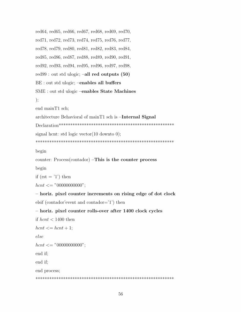
red64, red65, red66, red67, red68, red69, red70,
red71, red72, red73, red74, red75, red76, red77,
red78, red79, red80, red81, red82, red83, red84,
red85, red86, red87, red88, red89, red90, red91,
red92, red93, red94, red95, red96, red97, red98,
red99 : out std ulogic; –all red outputs (50)
BE : out std ulogic; –enables all buffers
SME : out std ulogic –enables State Machines
);
end mainT1 sch;
architecture Behavioral of mainT1 sch is –Internal Signal
Declaration**************************************************
signal hcnt: std logic vector(10 downto 0);
************************************************************
begin
counter: Process(contador) –This is the counter process
begin
if (rst = ’1’) then
hcnt <= ”00000000000”;
– horiz. pixel counter increments on rising edge of dot clock
elsif (contador’event and contador=’1’) then
– horiz. pixel counter rolls-over after 1400 clock cycles
if hcnt < 1400 then
hcnt <= hcnt + 1;
else
hcnt <= ”00000000000”;
end if;
end if;
end process;
************************************************************
56

Laser0: Process(hcnt)
begin
if (hcnt = 102) then –Laser 0 procedure
red0 <= rin0;
red1 <= rin1;
end if;
end process;
*************************************************************
*
*
*
*************************************************************
Laser49: Process(hcnt)
begin
if (hcnt = 494) then –Laser 49 procedure
red98 <= rin0;
red99 <= rin1;
end if;
end process;
*************************************************************
Enable: Process(hcnt)
begin
if (hcnt = 494 or hcnt = 495) then –Buffer Enable
BE <=′ 1′;
else
BE <=′ 0′;
end if;
end process;
*************************************************************
SMEnable: Process(hcnt)
57

begin
if (hcnt = 415 or hcnt = 416) then –Tri State Enable
SME <= ’1’; – and Clock Enable for SME
else
SME <=′ 0′;
end if;
end process;
end Behavioral;
B.0.6 Main Driver 2
The original name of this submodule is ”mainT2 sch”. The code is shown below:
library IEEE;
use IEEE.STD LOGIC 1164.ALL;
use IEEE.STD LOGIC ARITH.ALL;
use IEEE.STD LOGIC UNSIGNED.ALL;
–This is the main driver that controls all 50 lasers.
At time T1, pixels p3, p7, p11, p15, p19 etc... are lit at this
time. Buffer T2 will gather all the information for these pixels
entity mainT2 sch is
Port (
contador : in std ulogic; –internal counter
rst : in std ulogic; –async reset input
hsyncin : in std ulogic; –horizontal sync input
vsyncin : in std ulogic; –vertical sync input
rin0 : in std ulogic; –MSB for Red input
rin1 : in std ulogic; –LSB for Red input (out of 2 bits)
red0, red1, red2, red3, red4, red5, red6, red7,
red8, red9, red10, red11, red12, red13, red14,
red15, red16, red17, red18, red19, red20, red21,
58

red22, red23, red24, red25, red26, red27, red28,
red29, red30, red31, red32, red33, red34, red35,
red36, red37, red38, red39, red40, red41, red42,
red43, red44, red45, red46, red47, red48, red49,
red50, red51, red52, red53, red54, red55, red56,
red57, red58, red59, red60, red61, red62, red63,
red64, red65, red66, red67, red68, red69, red70,
red71, red72, red73, red74, red75, red76, red77,
red78, red79, red80, red81, red82, red83, red84,
red85, red86, red87, red88, red89, red90, red91,
red92, red93, red94, red95, red96, red97, red98,
red99 : out std ulogic; –all red outputs (50)
BE : out std ulogic; –enables all buffers
SME : out std ulogic –enables State Machines
);
end mainT2 sch;
architecture Behavioral of mainT2 sch is –Internal Signal
Declaration**************************************************
signal hcnt: std logic vector(10 downto 0);
************************************************************
begin
counter: Process(contador) –This is the counter process
begin
if (rst = ’1’) then
hcnt <= ”00000000000”;
– horiz. pixel counter increments on rising edge of dot clock
elsif (contador’event and contador=’1’) then
– horiz. pixel counter rolls-over after 1400 clock cycles
if hcnt < 1400 then
hcnt <= hcnt + 1;
59

else
hcnt <= ”00000000000”;
end if;
end if;
end process;
************************************************************
Laser0: Process(hcnt)
begin
if (hcnt = 104) then –Laser 0 procedure
red0 <= rin0;
red1 <= rin1;
end if;
end process;
*************************************************************
*
*
*
*************************************************************
Laser49: Process(hcnt)
begin
if (hcnt = 496) then –Laser 49 procedure
red98 <= rin0;
red99 <= rin1;
end if;
end process;
*************************************************************
Enable: Process(hcnt)
begin
if (hcnt = 496 or hcnt = 497) then –Buffer Enable
BE <=′ 1′;
60

else
BE <=′ 0′;
end if;
end process;
*************************************************************
SMEnable: Process(hcnt)
begin
if (hcnt = 732 or hcnt = 733) then –Tri State Enable
SME <= ’1’; – and Clock Enable for SME
else
SME <=′ 0′;
end if;
end process;
end Behavioral;
B.0.7 Main Driver 3
The original name of this submodule is ”mainT3 sch”. The code is shown below:
library IEEE;
use IEEE.STD LOGIC 1164.ALL;
use IEEE.STD LOGIC ARITH.ALL;
use IEEE.STD LOGIC UNSIGNED.ALL;
–This is the main driver that controls all 50 lasers.
At time T1, pixels p4, p8, p12, p16, p20 etc... are lit at this
time. Buffer T3 will gather all the information for these pixels
entity mainT3 sch is
Port (
contador : in std ulogic; –internal counter
rst : in std ulogic; –async reset input
hsyncin : in std ulogic; –horizontal sync input
61

vsyncin : in std ulogic; –vertical sync input
rin0 : in std ulogic; –MSB for Red input
rin1 : in std ulogic; –LSB for Red input (out of 2 bits)
red0, red1, red2, red3, red4, red5, red6, red7,
red8, red9, red10, red11, red12, red13, red14,
red15, red16, red17, red18, red19, red20, red21,
red22, red23, red24, red25, red26, red27, red28,
red29, red30, red31, red32, red33, red34, red35,
red36, red37, red38, red39, red40, red41, red42,
red43, red44, red45, red46, red47, red48, red49,
red50, red51, red52, red53, red54, red55, red56,
red57, red58, red59, red60, red61, red62, red63,
red64, red65, red66, red67, red68, red69, red70,
red71, red72, red73, red74, red75, red76, red77,
red78, red79, red80, red81, red82, red83, red84,
red85, red86, red87, red88, red89, red90, red91,
red92, red93, red94, red95, red96, red97, red98,
red99 : out std ulogic; –all red outputs (50)
BE : out std ulogic; –enables all buffers
SME : out std ulogic –enables State Machines
);
end mainT3 sch;
architecture Behavioral of mainT3 sch is –Internal Signal
Declaration**************************************************
signal hcnt: std logic vector(10 downto 0);
************************************************************
begin
counter: Process(contador) –This is the counter process
begin
if (rst = ’1’) then
62

hcnt <= ”00000000000”;
– horiz. pixel counter increments on rising edge of dot clock
elsif (contador’event and contador=’1’) then
– horiz. pixel counter rolls-over after 1400 clock cycles
if hcnt < 1400 then
hcnt <= hcnt + 1;
else
hcnt <= ”00000000000”;
end if;
end if;
end process;
************************************************************
Laser0: Process(hcnt)
begin
if (hcnt = 106) then –Laser 0 procedure
red0 <= rin0;
red1 <= rin1;
end if;
end process;
*************************************************************
*
*
*
*************************************************************
Laser49: Process(hcnt)
begin
if (hcnt = 498) then –Laser 49 procedure
red98 <= rin0;
red99 <= rin1;
end if;
63

end process;
*************************************************************
Enable: Process(hcnt)
begin
if (hcnt = 498 or hcnt = 499) then –Buffer Enable
BE <=′ 1′;
else
BE <=′ 0′;
end if;
end process;
*************************************************************
SMEnable: Process(hcnt)
begin
if (hcnt = 1049 or hcnt = 1050) then –Tri State Enable
SME <= ’1’; – and Clock Enable for SME
else
SME <=′ 0′;
end if;
end process;
end Behavioral;
B.0.8 Three-State Buffer
In this section the three-state buffer was divided into two submodules which are the
”buffer” and the ”three-state” submodules. The reason why it was chosen that
way was because it was better to handle the variables by separate. The submodule
”buffer” works as a local memory and stores the data information until the ”BE”
(Buffer Enable) signal triggers the buffer and transfers the data to the three-state
submodule. This last submodule is like a stand by memory which is always at high
impedance until SME (State Machine Enable) signal triggers this submodule and
64

transfers the data to the laser actuator (laser act).
Buffer (Buf50L)
library IEEE;
use IEEE.STD LOGIC 1164.ALL;
use IEEE.STD LOGIC ARITH.ALL;
use IEEE.STD LOGIC UNSIGNED.ALL;
entity Buf50L is
Port (
BE : in std ulogic; –Enables Buffer
rin0, rin1, rin2, rin3, rin4, rin5, rin6, rin7,
rin8, rin9, rin10, rin11, rin12, rin13, rin14,
rin15, rin16, rin17, rin18, rin19, rin20, rin21,
rin22, rin23, rin24, rin25, rin26, rin27, rin28,
rin29, rin30, rin31, rin32, rin33, rin34, rin35,
rin36, rin37, rin38, rin39, rin40, rin41, rin42,
rin43, rin44, rin45, rin46, rin47, rin48,
rin49 : in std ulogic; –Buffer inputs
rout0, rout1, rout2, rout3, rout4, rout5, rout6,
rout7, rout8, rout9, rout10, rout11, rout12,
rout13, rout14, rout15, rout16, rout17, rout18,
rout19, rout20, rout21, rout22, rout23, rout24,
rout25, rout26, rout27, rout28, rout29, rout30,
rout31, rout32, rout33, rout34, rout35, rout36,
rout37, rout38, rout39, rout40, rout41, rout42,
rout43, rout44, rout45, rout46, rout47, rout48,
rout49 : out std ulogic –Buffer outputs
);
65

end Buf50L;
architecture Behavioral of Buf50L is
begin
Process(BE)
begin
if BE = ’1’ then
rout0 <= rin0;
rout1 <= rin1;
∗∗∗rout48 <= rin48;
rout49 <= rin49;
end if;
end process;
end Behavioral;
Three State Buffer (Tristatebuff)
library IEEE;
use IEEE.STD LOGIC 1164.ALL;
use IEEE.STD LOGIC ARITH.ALL;
use IEEE.STD LOGIC UNSIGNED.ALL;
entity tristatebuff is
Port (
SME : in std ulogic; –Enables Buffer
rin0, rin1, rin2, rin3, rin4, rin5, rin6, rin7,
66

rin8, rin9, rin10, rin11, rin12, rin13, rin14,
rin15, rin16, rin17, rin18, rin19, rin20, rin21,
rin22, rin23, rin24, rin25, rin26, rin27, rin28,
rin29, rin30, rin31, rin32, rin33, rin34, rin35,
rin36, rin37, rin38, rin39, rin40, rin41, rin42,
rin43, rin44, rin45, rin46, rin47, rin48,
rin49 : in std ulogic; –Buffer inputs
rout0, rout1, rout2, rout3, rout4, rout5, rout6,
rout7, rout8, rout9, rout10, rout11, rout12,
rout13, rout14, rout15, rout16, rout17, rout18,
rout19, rout20, rout21, rout22, rout23, rout24,
rout25, rout26, rout27, rout28, rout29, rout30,
rout31, rout32, rout33, rout34, rout35, rout36,
rout37, rout38, rout39, rout40, rout41, rout42,
rout43, rout44, rout45, rout46, rout47, rout48,
rout49 : out std ulogic –Buffer outputs
);
end tristatebuff;
architecture Behavioral of tristatebuff is
begin Process(SME)
begin
if SME = ’1’ then
rout0 <= rin0;
rout1 <= rin1;
∗∗∗rout48 <= rin48;
rout49 <= rin49;
67

else
rout0 <=′ Z ′;
rout1 <=′ Z ′;
∗∗∗rout48 <=′ Z ′;
rout49 <=′ Z ′;
end if;
end process;
end Behavioral;
B.0.9 Laser Actuator
Better known as ”laser act”, this is how the state machines were declared.
library IEEE;
use IEEE.STD LOGIC 1164.ALL;
use IEEE.STD LOGIC ARITH.ALL;
use IEEE.STD LOGIC UNSIGNED.ALL;
entity laser act is
Port (
clk : in std ulogic; –Clock
rst : in std ulogic; –Async reset
rin0, rin1, rin2, rin3, rin4, rin5, rin6, rin7,
rin8, rin9, rin10, rin11, rin12, rin13, rin14,
rin15, rin16, rin17, rin18, rin19, rin20, rin21,
rin22, rin23, rin24, rin25, rin26, rin27, rin28,
rin29, rin30, rin31, rin32, rin33, rin34, rin35,
rin36, rin37, rin38, rin39, rin40, rin41, rin42,
rin43, rin44, rin45, rin46, rin47, rin48,
68

rin49 : in std ulogic; –Laser intensity MSB
SME : in std ulogic; –State Machine Enable
led0, led1, led2, led3, led4, led5,
led6, led7, led8, led9, led10, led11, led12, led13,
led14, led15, led16, led17, led18, led19, led20,
led21, led22, led23,
led24 : out std ulogic –Laser outputs
);
end laser act;
architecture Behavioral of laser act is
signal hcnt: std logic vector(8 downto 0);
begin
counter: Process(clk) –This is the counter process begin
if (rst = ’1’) then
hcnt <= ”000000000”;
– horiz. pixel counter increments on rising edge of dot clock
elsif (clk’event and clk=’1’) then
– horiz. pixel counter rolls-over after 316 clock cycles
if hcnt<316 then
hcnt <= hcnt + 1;
else
hcnt <= ”000000000”;
end if;
end if;
end process;
********************************************************
69

–State Machines for all lasers;
********************************************************
–Laser 0
laser0: process(clk, hcnt, rin0, rin1, SME)
type state type is (High, Medium, Low, Off); –Declare Laser States
variable laser state: state type;
begin
if (rin0 = ’0’ and rin1 = ’0’ and SME = ’1’) then –When the red inputs are in
low
led0 <= ’0’ after 1 ns; –The laser is then Off
laser state := Off;
–default conditions
elsif (clk’event and clk = ’1’) then
led0 <= ’0’ after 1 ns;
–Define state transitions, note that end if is at the very end!
case laser state is
when Off =>
–Transition from Off to High
if (rin0 = ’1’ and rin1 = ’1’ and SME = ’1’) then
led0 <= ’1’ after 1 ns;
laser state := High;
–Transition from Off to Medium
elsif (rin0 = ’1’ and rin1 = ’0’ and SME = ’1’) then
led0 <= ’1’ after 1ns;
laser state := Medium;
–Transition from Off to Low
elsif (rin0 = ’0’ and rin1 = ’1’ and SME = ’1’) then
led0 <= ’1’ after 1ns;
laser state := Low; –Holding term in off
else
70

laser state := Off;
end if;
–This state makes the Laser be on for 314 clock cycles because is at High
state
when High =>
–Transition from High to Off
if (hcnt> 314) then
led0 <= ’0’ after 1ns;
laser state := Off;
–Holding term in High
else
led0 <= ’1’ after 1ns;
laser state := High;
end if;
–This state makes the Laser be on for 157 clock cycles because is at
Medium state
when Medium =>
–Transition from Medium to Off
if (hcnt>157) then
led0 <= ’0’ after 1ns;
laser state := Off;
–Holding term in Medium
else
led0 <= ’1’ after 1ns;
laser state := Medium;
end if;
–This state makes the Laser be on for 79 clock cycles because is at Low
state
when Low =>
–Transition from Low to Off
71

if (hcnt>79) then
led0 <= ’0’ after 1ns;
laser state := Off;
–Holding term in Low
else
led0 <= ’1’ after 1ns;
laser state := Low;
end if;
–Default term for dead states
when others =>
laser state := Off;
end case;
end if;
end process laser0;
*
*
*
***********************************************************************
–Laser 24
laser24: process(clk, hcnt, rin48, rin49, SME)
type state type is (High, Medium, Low, Off); –Declare Laser States
variable laser state: state type;
begin
if (rin48 = ’0’ and rin49 = ’0’ and SME = ’1’) then –When the red inputs are in
low
led24 <= ’0’ after 1 ns; –The laser is then Off
laser state := Off;
–default conditions
elsif (clk’event and clk = ’1’) then
led24 <= ’0’ after 1 ns;
72

–Define state transitions, note that end if is at the very end!
case laser state is
when Off =>
–Transition from Off to High
if (rin48 = ’1’ and rin49 = ’1’ and SME = ’1’) then
led24 <= ’1’ after 1 ns;
laser state := High;
–Transition from Off to Medium
elsif (rin48 = ’1’ and rin49 = ’0’ and SME = ’1’) then
led24 <= ’1’ after 1ns;
laser state := Medium;
–Transition from Off to Low
elsif (rin48 = ’0’ and rin49 = ’1’ and SME = ’1’) then
led24 <= ’1’ after 1ns;
laser state := Low; –Holding term in off
else
laser state := Off;
end if;
–This state makes the Laser be on for 314 clock cycles because is at High
state
when High =>
–Transition from High to Off
if (hcnt> 314) then
led24 <= ’0’ after 1ns;
laser state := Off;
–Holding term in High
else
led24 <= ’1’ after 1ns;
laser state := High;
end if;
73

–This state makes the Laser be on for 157 clock cycles because is at
Medium state
when Medium =>
–Transition from Medium to Off
if (hcnt>157) then
led24 <= ’0’ after 1ns;
laser state := Off;
–Holding term in Medium
else
led24 <= ’1’ after 1ns;
laser state := Medium;
end if;
–This state makes the Laser be on for 79 clock cycles because is at Low
state
when Low =>
–Transition from Low to Off
if (hcnt>79) then
led24 <= ’0’ after 1ns;
laser state := Off;
–Holding term in Low
else
led24 <= ’1’ after 1ns;
laser state := Low;
end if;
–Default term for dead states
when others =>
laser state := Off;
end case;
end if;
end process laser24;
74

end Behavioral;
B.0.10 FPGA Pin out
NET ”clkout” LOC = ”P64” ;
NET ”vsyncout” LOC = ”P62” ;
NET ”vsyncin” LOC = ”P189” ;
NET ”rout1” LOC = ”P74” ;
NET ”rout0” LOC = ”P73” ;
NET ”rin1” LOC = ”P192” ;
NET ”rin0” LOC = ”P193” ;
NET ”led49” LOC = ”P154” ;
NET ”led48” LOC = ”P160” ;
NET ”led47” LOC = ”P161” ;
NET ”led46” LOC = ”P162” ;
NET ”led45” LOC = ”P163” ;
NET ”led44” LOC = ”P164” ;
NET ”led43” LOC = ”P165” ;
NET ”led42” LOC = ”P166” ;
NET ”led41” LOC = ”P167” ;
NET ”led40” LOC = ”P168” ;
NET ”led39” LOC = ”P169” ;
NET ”led38” LOC = ”P173” ;
NET ”led37” LOC = ”P174” ;
NET ”led36” LOC = ”P175” ;
NET ”led35” LOC = ”P176” ;
NET ”led34” LOC = ”P178” ;
NET ”led33” LOC = ”P179” ;
NET ”led32” LOC = ”P108” ;
NET ”led31” LOC = ”P102” ;
75

NET ”led30” LOC = ”P110” ;
NET ”led29” LOC = ”P109” ;
NET ”led28” LOC = ”P112” ;
NET ”led27” LOC = ”P111” ;
NET ”led26” LOC = ”P114” ;
NET ”led25” LOC = ”P113” ;
NET ”led24” LOC = ”P116” ;
NET ”led23” LOC = ”P115” ;
NET ”led22” LOC = ”P121” ;
NET ”led21” LOC = ”P120” ;
NET ”led20” LOC = ”P123” ;
NET ”led19” LOC = ”P122” ;
NET ”led18” LOC = ”P125” ;
NET ”led17” LOC = ”P81” ;
NET ”led16” LOC = ”P75” ;
NET ”led15” LOC = ”P83” ;
NET ”led14” LOC = ”P82” ;
NET ”led13” LOC = ”P86” ;
NET ”led12” LOC = ”P84” ;
NET ”led11” LOC = ”P88” ;
NET ”led10” LOC = ”P87” ;
NET ”led9” LOC = ”P93” ;
NET ”led8” LOC = ”P89” ;
NET ”led7” LOC = ”P95” ;
NET ”led6” LOC = ”P94” ;
NET ”led5” LOC = ”P97” ;
NET ”led4” LOC = ”P96” ;
NET ”led3” LOC = ”P99” ;
NET ”led2” LOC = ”P98” ;
NET ”led1” LOC = ”P101” ;
76

NET ”led0” LOC = ”P100” ;
NET ”hsyncout” LOC = ”P70” ;
NET ”hsyncin” LOC = ”P63” ;
NET ”clock” LOC = ”P80” ;
NET ”SME0” LOC = ”P61”;
NET ”SME1” LOC = ”P60”;
NET ”SME2” LOC = ”P59”;
NET ”SME3” LOC = ”P58”;
NET ”integra” LOC = ”P152”;
77

78

Bibliography
[1] http://useurotek.com/docs/piezomechanik/stack.htm.
[2] Choquette K.D.; Fischer A. J.; Blum O.; Allerman A. A. Continuous wave
operation of 1.3 µm vertical cavity ingaasn quantum well lasers. IEEE 17th
International Semiconductor Laser Conference, pages 7–8, September 2000.
[3] Adaptronics. http://www.adaptronics.com/products/piezoelectricactuators/
directactuators/ppam.html.
[4] C. E. Baker. Laser display technology. IEEE Spectrum, pages 39–50, December
1968.
[5] Lincoln Laser Company. Polygon Size Calculation. Lincoln Laser Company, 234
East Mohave St; Phoenix Arizona.
[6] J. K. Guenter et al. Commercialization of honeywell’s vcsel technology: Further
developments. Proceedings of the SPIE, 4286, 2001.
[7] S. Kiiskila et al. Compact laser projector for multimedia. Proc. European Multi-
media, Embedded Systems, and electronic Commerce Conference (EMMSEC’99),
Stockholm, Sweden 1999.
[8] J. L. Jewell; J. P. Harbison; A. Scherer; Y. H. Lee; L. T. Florez. Vertical-cavity
surface-emitting lasers: Design, growth, fabrication, characterization. IEEE J.
Quantum Electronics, 27:13321346, 1991.
79

[9] J. L. Jewell; Y. H. Lee; S. L. McCall; J. P. Harbison; L.T. Florez. High-finesse
(al,ga)as interference filters grown by molecular beam epitaxy. Appl. Phys. Lett.,
53:640642, 1988.
[10] Xilinx Foundation. http://www.xilinx.com.
[11] P. L. Gourley and T. J. Drummond. Single crystal epitaxial multilayers of alas
gaas and alxga1-xas for use as optical interferometric elements. Appl. Phys. Lett.,
49:489491, 1986.
[12] W. W. Chow; K. D. Choquette; M. H. Crawford; K. L. Lear; G. R. Hadley. De-
sign, fabrication, and performance of infrared and visible vertical-cavity surface
emitting lasers. IEEE J. Quantum. Electronics, 33:18101823, 1997.
[13] Eugene Hecht. OPTICS, volume 1. Addison Wesley, fourth edition, 2002.
[14] Choquette K.D.; Hou H.Q. Proceedings of the ieee. 85(11):1730 –1739, November
1997.
[15] V. M. Bove Jr. Connected by media. IEEE Multimedia 8:4, Oct-Dec. 2001.
[16] Zonghe Lai and Johan Liu. Wire bonding. http://extra.ivf.se/ngl/A-
WireBonding/ChapterA1.htm#A1.1.
[17] Jae S. Lim. Two Dimensional Signal and Image Processing. Prentice Hall, Upper
Saddle River, New Jersey 07458, 1990. Pp 416-421.
[18] Y. H. Lo; R. Bhat; D. M. Hwang; C. Chua; C. H. Lin. Semiconductor lasers on
si substrates using the technology of bonding by atomic rearrangement. Appl.
Phys. Lett., 62:10381040, 1993.
[19] Morgan R.A. Vertical-cavity lasers technologies for a global information infras-
tructure. 1997 Digest of the IEEE/LEOS Summer Topical Meetings, pages 5–6,
August 1997.
80

[20] Larson M. C.; Coldren C. W.; Spruyette S. G.; Petersen H. E.; Harris J. S. Low
threshold current continuous-wave gainnas/gaas vcsels. IEEE 17th International
Semiconductor Laser Conference, pages 9–10, Setptember 2000.
[21] Symbol Technologies. Laser projection display.
http://www.symbol.com/products/oem/lpd.html.
[22] Kranert J.; Deter C.; Gessner T.; Dotzel W. Laser display technology. The
Eleventh Annual International Workshop Proceedings, pages 99 –104, 1998. Micro
Electro Mechanical Systems, 1998. MEMS 98.
[23] Eran Sabo Zeev Zalevsky, Yuval Kapelner and Sharon Kapelner. Virtual display
with low power consuming, portable micro projector. SPIE, 5002:154 – 163,
2003.
81