micro-power data converters -...
TRANSCRIPT
[email protected]@ece.orst.edu
Micro-Power Data Converters
Gabor C. Temes
School of EECS
Oregon State University
1/68
[email protected]@ece.orst.edu
Outline
• Micro-power D/A converters:
- Overview of CMOS DACs
- Switched-capacitor DACs
- Quasi-passive two-C DAC
- Quasi-passive pipeline DAC
- Delta-sigma DACs.
• Micro-power A/D converters:
- Overview of CMOS ADCs
- SAR ADC, pipeline SAR ADC
- Multiplexed incremental ADC
- Extended-count hybrid ADC.
2/68
[email protected]@ece.orst.edu
Applications
• Battery-powered medical devices (hearing aids, ECG,
EEG, etc. sensors, brain stimulators) ;
• Wireless sensor networks for industrial and environmental
applications;
• RFID systems.
• Typical target specifications:
DACs: BW up to 20 kHz, ENOB 14 - 15 bits, 20-bit input ;
ADCs: BW = up to 5 kHz; ENOB > 12 bits; power < 5
microwatts; input signal amplitude 0.1 ~ 5 mV.
3/68
[email protected]@ece.orst.edu
Power Saving in Data Converters
• Stages: S/Hs, buffers, comparators, SC blocks.
• S/H: whenever possible, use passive (SC) circuitry; if
not, use direct charge transfer (DCT) amplifier stage.
• Buffers: use DCT stage.
• Comparators: use dynamic circuitry.
• SC circuits: use minimally busy circuitry. Reduce
dynamic power dissipation.
• Transistor circuits: consider weak inversion
operation.
• Logic: consider asynchronous switching.
4/68
[email protected]@ece.orst.edu
Classification of DACs
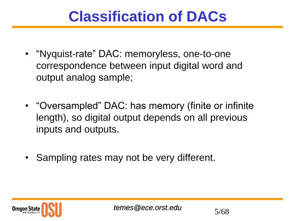
• “Nyquist-rate” DAC: memoryless, one-to-one
correspondence between input digital word and
output analog sample;
• “Oversampled” DAC: has memory (finite or infinite
length), so digital output depends on all previous
inputs and outputs.
• Sampling rates may not be very different.
5/68
[email protected]@ece.orst.edu
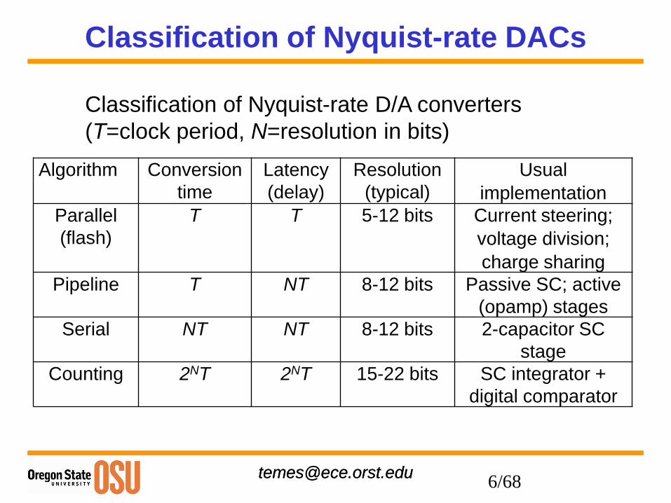
Classification of Nyquist-rate DACs
Algorithm Conversion
time
Latency
(delay)
Resolution
(typical)
Usual
implementation
Parallel
(flash)
T T 5-12 bits Current steering;
voltage division;
charge sharing
Pipeline T NT 8-12 bits Passive SC; active
(opamp) stages
Serial NT NT 8-12 bits 2-capacitor SC
stage
Counting 2NT 2NT 15-22 bits SC integrator +
digital comparator
Classification of Nyquist-rate D/A converters
(T=clock period, N=resolution in bits)
6/68
[email protected]@ece.orst.edu
Nyquist-Rate DACs
• Parallel (flash) DACs: conversion time and latency is
T; resolution N < 10 bits; implementation R-string or
R-2R ladder, current sources, switched-capacitor
(SC) stage.
• Pipelined DACs: conversion time T; latency NT;
N < 14 bits; SC stages.
• Serial DACs: conversion time and latency NT;
N < 12 bits; 2-C stages.
• Counting DAC: conversion time and latency = 2N.T;
N < 24 bits; SC or RC integrators.
7/68
[email protected]@ece.orst.edu
Oversampled CMOS DACs
• Nyquist-rate vs. oversampled DACs: in oversampled
DAC, the word length can be reduced to 1 ~ 5 bits.
• Mismatch errors can be suppressed in signal band
using dynamic element matching.
• High accuracy can be obtained with simple low-
power analog circuitry, but complex digital delta-
sigma loop and prefilter are required.
• May only be economical for high-resolution low-
power DAC applications.
8/68
[email protected]@ece.orst.edu
Nyquist-Rate Parallel DACs
• R-string or R-2R ladder: large area, large mismatch
errors, static dissipation – seldom practical in low-
power applications.
• Current-source DAC: large mismatch error, static
dissipation – seldom used in slow low-power DACs.
• SC stages: binary-weighted or unary (unit-element-
based) charge redistribution circuits. Unary is more
complex, but the glitches are reduced, the
monotonicity is guaranteed, and dynamic element
matching may be possible.
9/68
[email protected]@ece.orst.edu
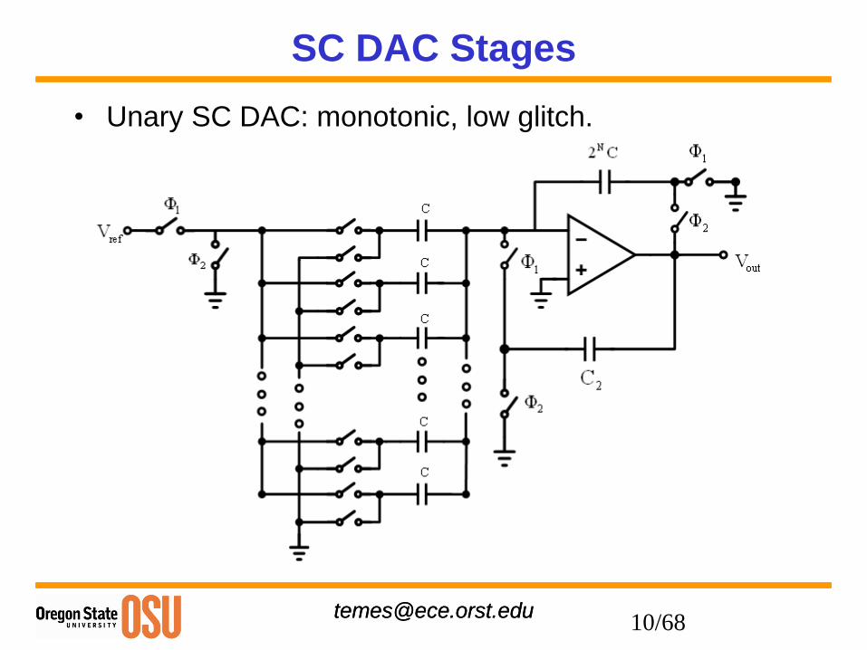
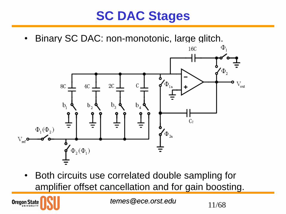
SC DAC Stages
• Binary SC DAC: non-monotonic, large glitch.
• Both circuits use correlated double sampling for
amplifier offset cancellation and for gain boosting.
11/68
[email protected]@ece.orst.edu
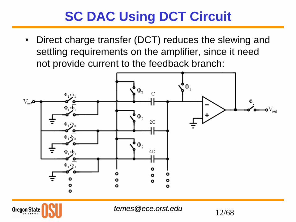
SC DAC Using DCT Circuit
• Direct charge transfer (DCT) reduces the slewing and
settling requirements on the amplifier, since it need
not provide current to the feedback branch:
12/68
[email protected]@ece.orst.edu
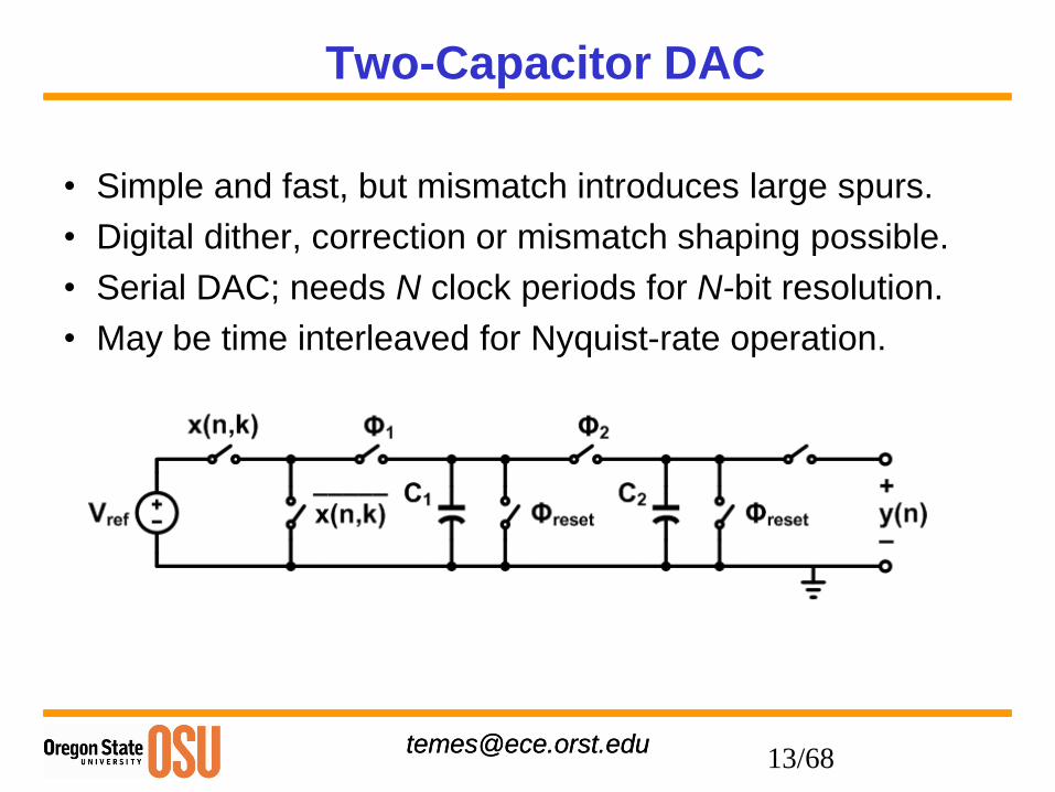
Two-Capacitor DAC
• Simple and fast, but mismatch introduces large spurs.
• Digital dither, correction or mismatch shaping possible.
• Serial DAC; needs N clock periods for N-bit resolution.
• May be time interleaved for Nyquist-rate operation.
13/68
[email protected]@ece.orst.edu
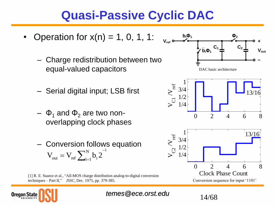
Quasi-Passive Cyclic DAC
• Operation for x(n) = 1, 0, 1, 1:
– Charge redistribution between two
equal-valued capacitors
– Serial digital input; LSB first
– Φ1 and Φ2 are two non-
overlapping clock phases
– Conversion follows equation
Φ2
C1 C2
Vref
_biΦ1 Vout
+
–
biΦ1
iN
1i irefout 2bVV
DAC basic architecture
Conversion sequence for input „1101‟
0 2 4 6 8
1/4
1/2
3/4
1
VC
1 /
Vre
f
13/16
0 2 4 6 8
1/4
1/2
3/4
1
VC
2 /
Vre
f 13/16
Clock Phase Count[1] R. E. Suarez et al., “All-MOS charge distribution analog-to-digital conversion
techniques – Part II,” JSSC, Dec. 1975, pp. 379-385.
14/68
[email protected]@ece.orst.edu
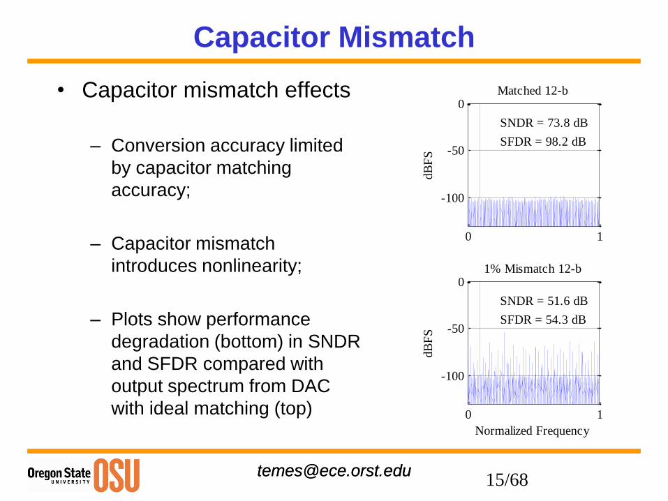
Capacitor Mismatch
• Capacitor mismatch effects
– Conversion accuracy limited
by capacitor matching
accuracy;
– Capacitor mismatch
introduces nonlinearity;
– Plots show performance
degradation (bottom) in SNDR
and SFDR compared with
output spectrum from DAC
with ideal matching (top)
0 1
-100
-50
0
dB
FS
Matched 12-b
SNDR = 73.8 dB
SFDR = 98.2 dB
0 1
-100
-50
0
dB
FS
1% Mismatch 12-b
Normalized Frequency
SNDR = 51.6 dB
SFDR = 54.3 dB
15/68
[email protected]@ece.orst.edu
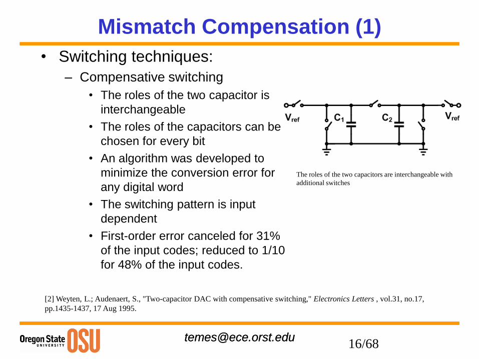
Mismatch Compensation (1)
• Switching techniques:
– Compensative switching
• The roles of the two capacitor is
interchangeable
• The roles of the capacitors can be
chosen for every bit
• An algorithm was developed to
minimize the conversion error for
any digital word
• The switching pattern is input
dependent
• First-order error canceled for 31%
of the input codes; reduced to 1/10
for 48% of the input codes.
[2] Weyten, L.; Audenaert, S., "Two-capacitor DAC with compensative switching," Electronics Letters , vol.31, no.17,
pp.1435-1437, 17 Aug 1995.
The roles of the two capacitors are interchangeable with
additional switches
16/68
[email protected]@ece.orst.edu
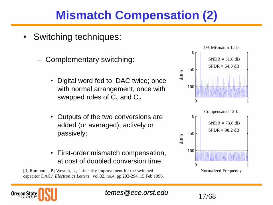
Mismatch Compensation (2)
• Switching techniques:
– Complementary switching:
• Digital word fed to DAC twice; once
with normal arrangement, once with
swapped roles of C1 and C2
• Outputs of the two conversions are
added (or averaged), actively or
passively;
• First-order mismatch compensation,
at cost of doubled conversion time.
[3] Rombouts, P.; Weyten, L., "Linearity improvement for the switched-
capacitor DAC," Electronics Letters , vol.32, no.4, pp.293-294, 15 Feb 1996.
0 1
-100
-50
0
dB
FS
Compensated 12-b
Normalized Frequency
SNDR = 73.8 dB
SFDR = 98.2 dB
0 1
-100
-50
0
dB
FS
1% Mismatch 12-b
SNDR = 51.6 dB
SFDR = 54.3 dB
17/68
[email protected]@ece.orst.edu
Mismatch Compensation (3)
• Switching techniques:
– Input-word-splitting compensative switching
• Compensative switching [2] does not compensate for all input
codes
• Split digital input into sum of two digital codes
• The conversion errors reduced using compensative switching
for the two new digital inputs
• Final output is the sum of the two conversions
-----------------------------------------
• Needs two sets of 2-C DACs
• Needs analog summation
• Needs sophisticated algorithm for splitting the input word
[4] Rombouts, P.; Weyten, L.; Raman, J.; Audenaert, S., "Capacitor mismatch compensation for the quasi-passive-
switched-capacitor DAC," Circuits and Systems I: Fundamental Theory and Applications, IEEE Transactions on ,
vol.45, no.1, pp.68-71, Jan 1998.
18/68
[email protected]@ece.orst.edu
Mismatch Compensation (4)
• Switching techniques
– Alternately complementary switching
• Roles of C1 and C2 are swapped alternately in the first cycle
and adopt complementary switching [3] for the second
conversion cycle
• Output of the two conversions are summed (or averaged)
• INL improved due to cancellation of major second-order error
– Hybrid switching
• Averaging conversion results of complementary switching and
alternately complementary switching
• Smaller INL; fourfold conversion cycles
[5] Poki Chen; Ting-Chun Liu, "Switching Schemes for Reducing Capacitor Mismatch Sensitivity of Quasi-Passive
Cyclic DAC," Circuits and Systems II: Express Briefs, IEEE Transactions on , vol.56, no.1, pp.26-30, Jan. 2009
19/68
[email protected]@ece.orst.edu
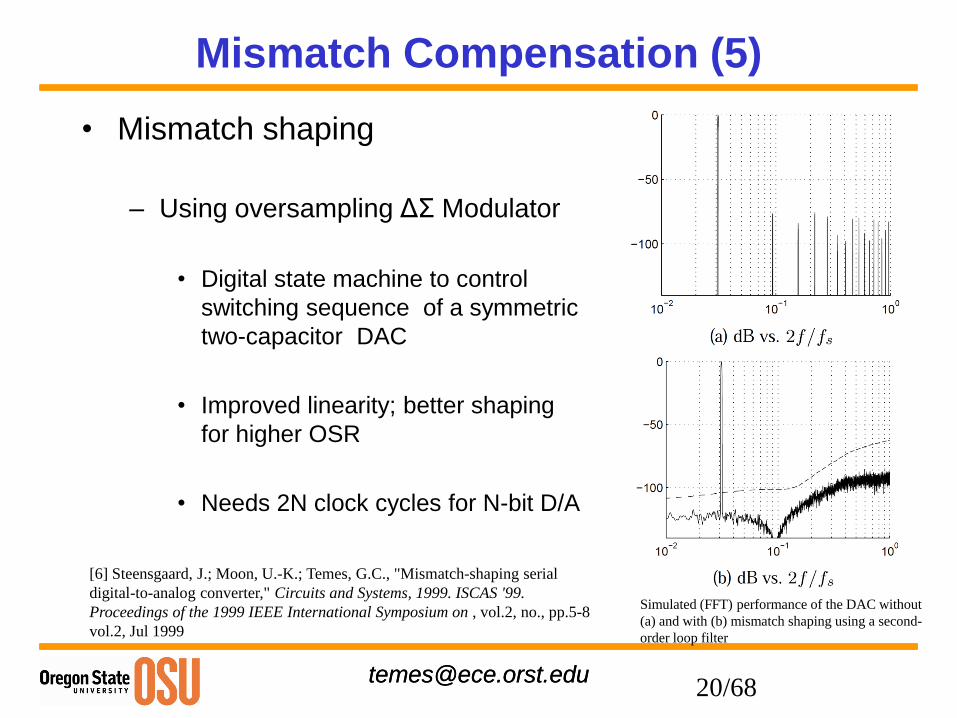
Mismatch Compensation (5)
• Mismatch shaping
– Using oversampling ΔΣ Modulator
• Digital state machine to control
switching sequence of a symmetric
two-capacitor DAC
• Improved linearity; better shaping
for higher OSR
• Needs 2N clock cycles for N-bit D/A
[6] Steensgaard, J.; Moon, U.-K.; Temes, G.C., "Mismatch-shaping serial
digital-to-analog converter," Circuits and Systems, 1999. ISCAS '99.
Proceedings of the 1999 IEEE International Symposium on , vol.2, no., pp.5-8
vol.2, Jul 1999
Simulated (FFT) performance of the DAC without
(a) and with (b) mismatch shaping using a second-
order loop filter
20/68
[email protected]@ece.orst.edu
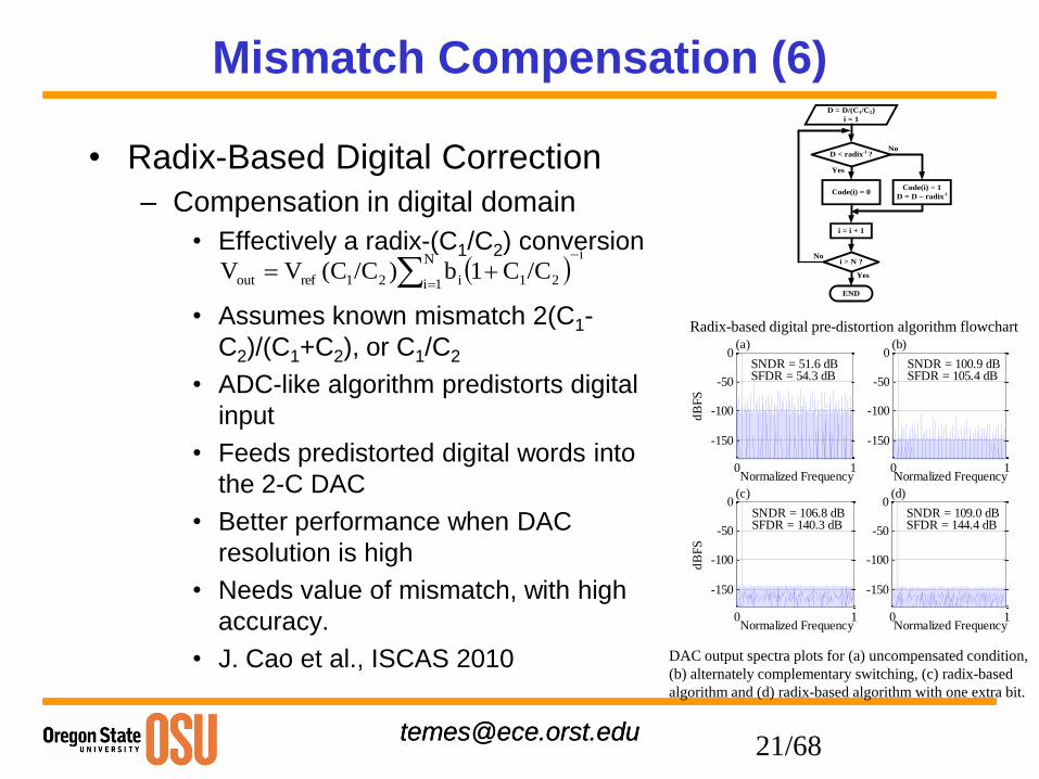
Mismatch Compensation (6)
• Radix-Based Digital Correction
– Compensation in digital domain
• Effectively a radix-(C1/C2) conversion
• Assumes known mismatch 2(C1-
C2)/(C1+C2), or C1/C2
• ADC-like algorithm predistorts digital
input
• Feeds predistorted digital words into
the 2-C DAC
• Better performance when DAC
resolution is high
• Needs value of mismatch, with high
accuracy.
• J. Cao et al., ISCAS 2010
D = D/(C1/C2)
i = 1
D < radix-i ?
Code(i) = 1
D = D – radix-iCode(i) = 0
i = i + 1
i > N ?
END
Yes
No
No
Yes
0 1
-150
-100
-50
0
dB
FS
(a)
Normalized Frequency
SNDR = 51.6 dBSFDR = 54.3 dB
0 1
-150
-100
-50
0(b)
Normalized Frequency
SNDR = 100.9 dBSFDR = 105.4 dB
0 1
-150
-100
-50
0
dB
FS
(c)
Normalized Frequency
SNDR = 106.8 dBSFDR = 140.3 dB
0 1
-150
-100
-50
0(d)
Normalized Frequency
SNDR = 109.0 dBSFDR = 144.4 dB
DAC output spectra plots for (a) uncompensated condition,
(b) alternately complementary switching, (c) radix-based
algorithm and (d) radix-based algorithm with one extra bit.
Radix-based digital pre-distortion algorithm flowchart
iN
1i 21i21refout /CC1b)/C(CVV
21/68
[email protected]@ece.orst.edu
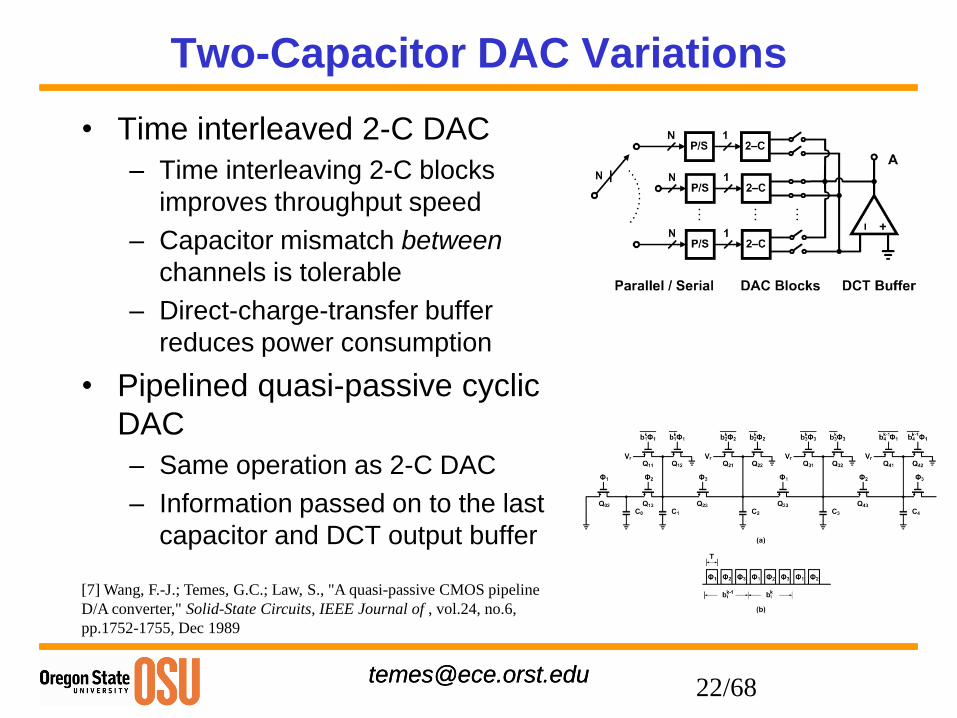
Two-Capacitor DAC Variations
• Time interleaved 2-C DAC
– Time interleaving 2-C blocks
improves throughput speed
– Capacitor mismatch between
channels is tolerable
– Direct-charge-transfer buffer
reduces power consumption
• Pipelined quasi-passive cyclic
DAC
– Same operation as 2-C DAC
– Information passed on to the last
capacitor and DCT output buffer
[7] Wang, F.-J.; Temes, G.C.; Law, S., "A quasi-passive CMOS pipeline
D/A converter," Solid-State Circuits, IEEE Journal of , vol.24, no.6,
pp.1752-1755, Dec 1989
22/68
[email protected]@ece.orst.edu
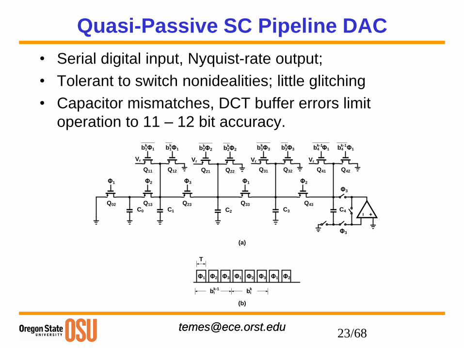
Quasi-Passive SC Pipeline DAC
• Serial digital input, Nyquist-rate output;
• Tolerant to switch nonidealities; little glitching
• Capacitor mismatches, DCT buffer errors limit
operation to 11 – 12 bit accuracy.
Vr
k
____
b1Φ1b1Φ1k
__
Vr
k
____
b2Φ2b2Φ2k
__
Vr
k
____
b3Φ3k
__
Vr
k-1
_____
b4 Φ1b4 Φ1k-1
___
b3Φ3
Q02
Q12 Q21 Q22 Q31 Q32 Q41 Q42
Φ2Φ1 Φ3 Φ2Φ1
Φ3
C0 C1 C2 C3 C4
Q13 Q23 Q33 Q43
(a)
Q11
Φ1 Φ2 Φ3 Φ1 Φ2 Φ3 Φ1 Φ2
bik-1
bik
T
(b)
Φ3
23/68
[email protected]@ece.orst.edu
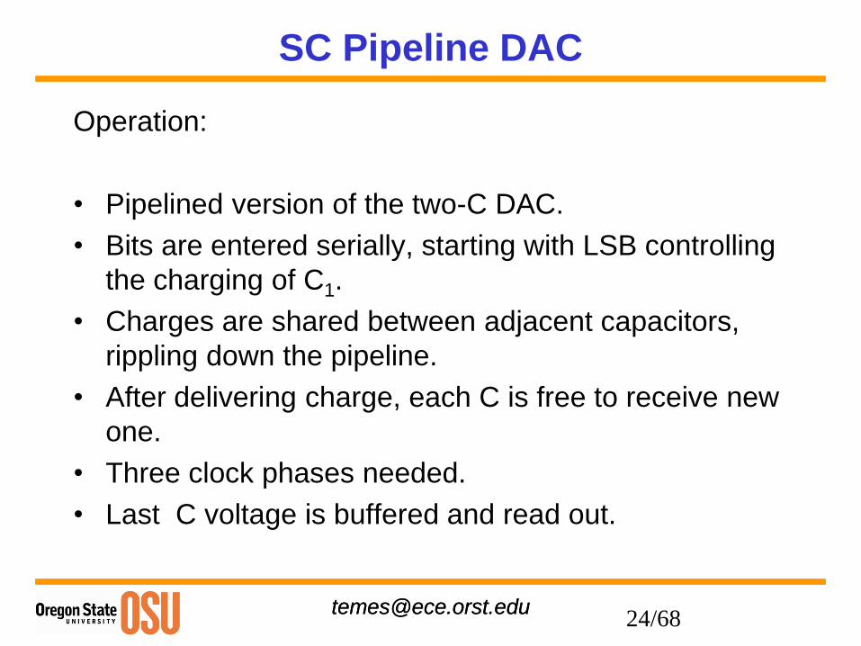
SC Pipeline DAC
Operation:
• Pipelined version of the two-C DAC.
• Bits are entered serially, starting with LSB controlling
the charging of C1.
• Charges are shared between adjacent capacitors,
rippling down the pipeline.
• After delivering charge, each C is free to receive new
one.
• Three clock phases needed.
• Last C voltage is buffered and read out.
24/68
[email protected]@ece.orst.edu
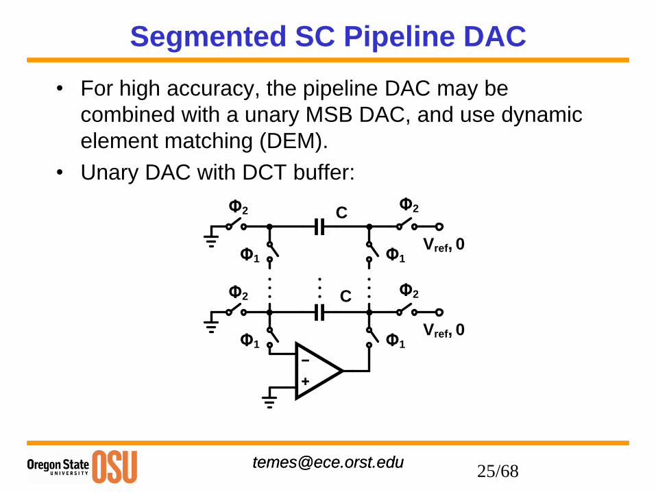
Segmented SC Pipeline DAC
• For high accuracy, the pipeline DAC may be
combined with a unary MSB DAC, and use dynamic
element matching (DEM).
• Unary DAC with DCT buffer:
Φ1Φ1
Φ2 Φ2
Vref, 0Φ1Φ1
Φ2 Φ2
C
C
Vref, 0
25/68
[email protected]@ece.orst.edu
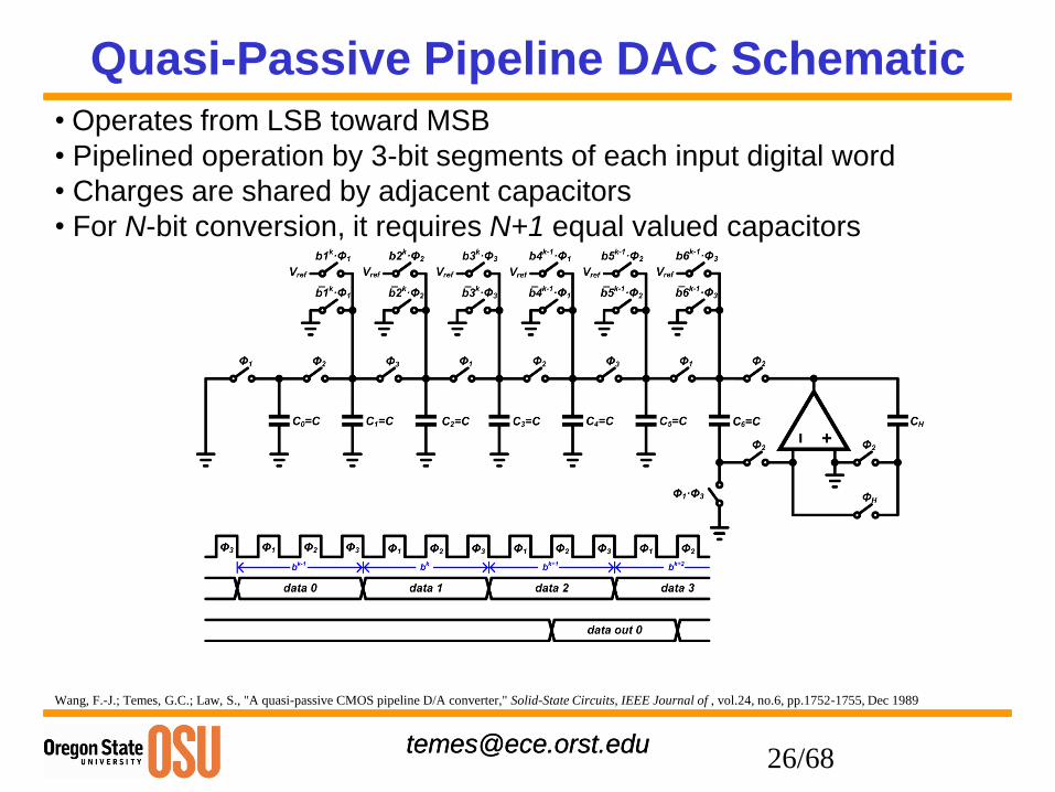
Quasi-Passive Pipeline DAC Schematic
• Operates from LSB toward MSB
• Pipelined operation by 3-bit segments of each input digital word
• Charges are shared by adjacent capacitors
• For N-bit conversion, it requires N+1 equal valued capacitors
Wang, F.-J.; Temes, G.C.; Law, S., "A quasi-passive CMOS pipeline D/A converter," Solid-State Circuits, IEEE Journal of , vol.24, no.6, pp.1752-1755, Dec 1989
26/68
[email protected]@ece.orst.edu
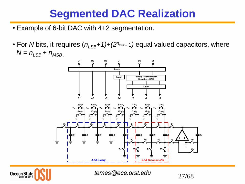
Segmented DAC Realization
• Example of 6-bit DAC with 4+2 segmentation.
• For N bits, it requires (nLSB+1)+(2nMSB - 1) equal valued capacitors, where
N = nLSB + nMSB .
27/68
[email protected]@ece.orst.edu
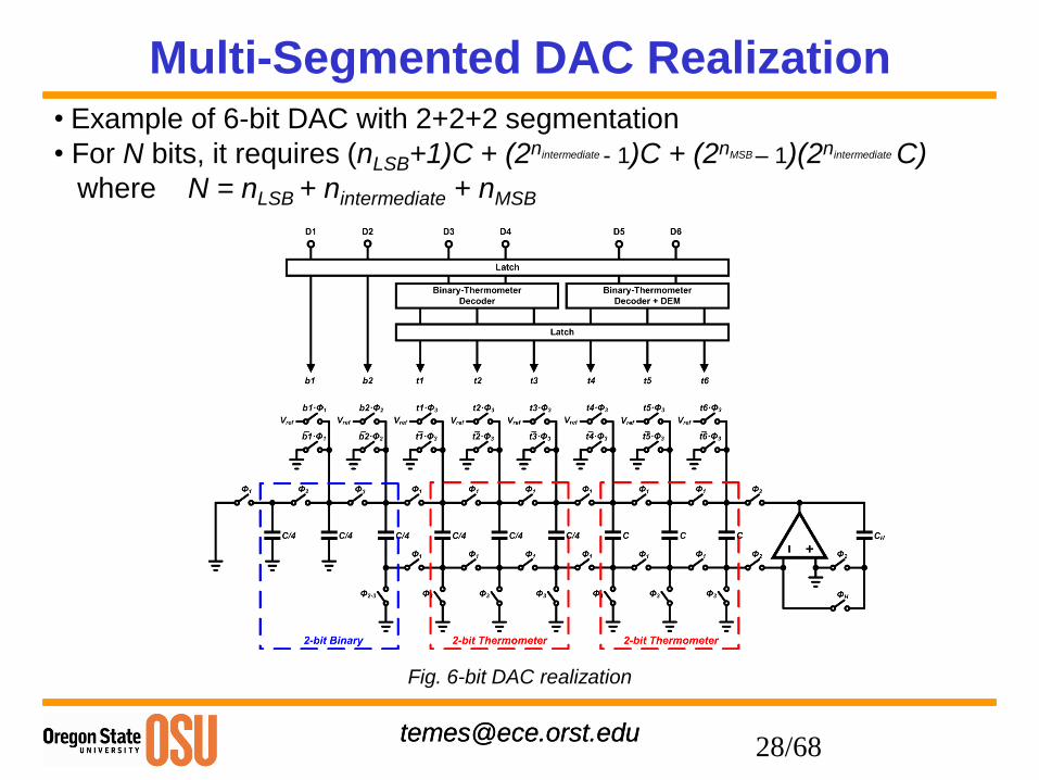
Multi-Segmented DAC Realization
Fig. 6-bit DAC realization
• Example of 6-bit DAC with 2+2+2 segmentation
• For N bits, it requires (nLSB+1)C + (2nintermediate - 1)C + (2nMSB – 1)(2nintermediate C)
where N = nLSB + nintermediate + nMSB
28/68
[email protected]@ece.orst.edu
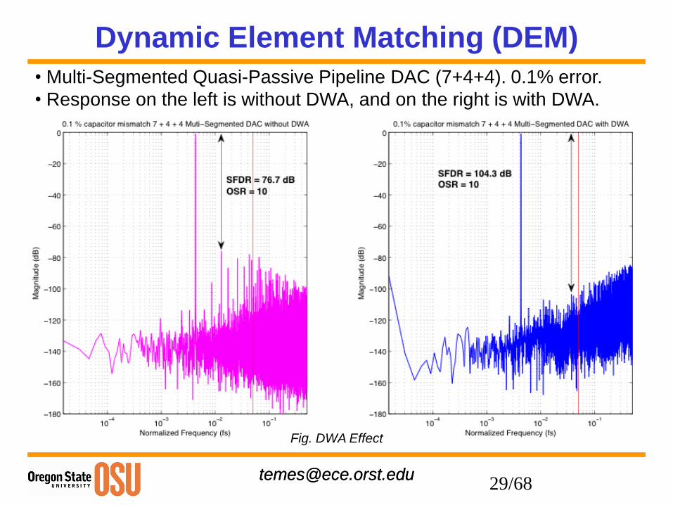
Dynamic Element Matching (DEM)
• Multi-Segmented Quasi-Passive Pipeline DAC (7+4+4). 0.1% error.
• Response on the left is without DWA, and on the right is with DWA.
Fig. DWA Effect
29/68
[email protected]@ece.orst.edu
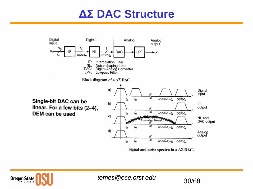
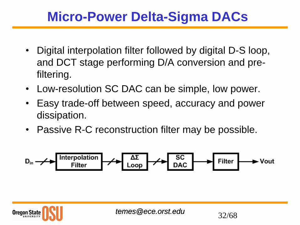
Micro-Power Delta-Sigma DACs
• Digital interpolation filter followed by digital D-S loop,
and DCT stage performing D/A conversion and pre-
filtering.
• Low-resolution SC DAC can be simple, low power.
• Easy trade-off between speed, accuracy and power
dissipation.
• Passive R-C reconstruction filter may be possible.
32/68
[email protected]@ece.orst.edu
Classification of ADCs
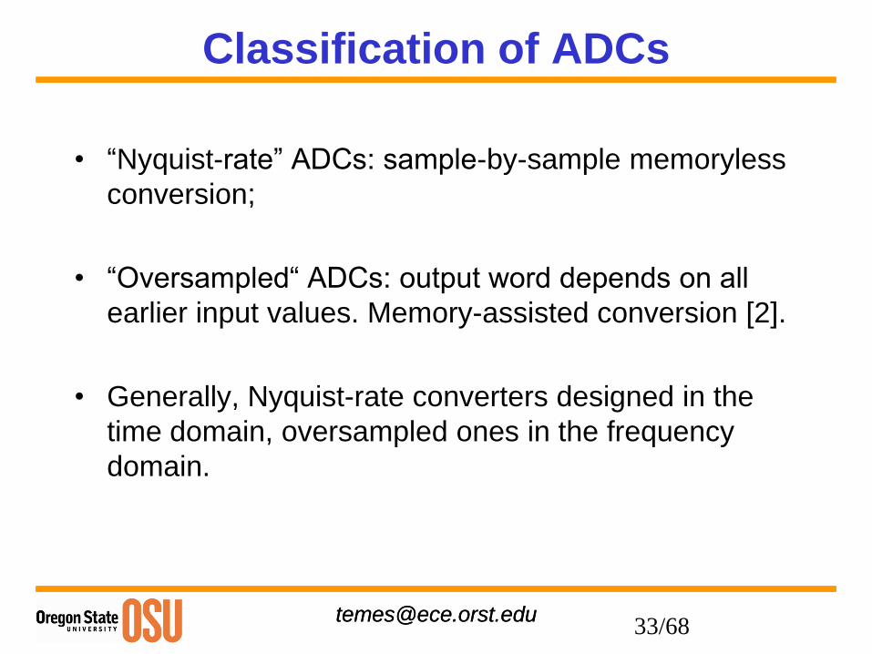
• “Nyquist-rate” ADCs: sample-by-sample memoryless
conversion;
• “Oversampled“ ADCs: output word depends on all
earlier input values. Memory-assisted conversion [2].
• Generally, Nyquist-rate converters designed in the
time domain, oversampled ones in the frequency
domain.
33/68
[email protected]@ece.orst.edu
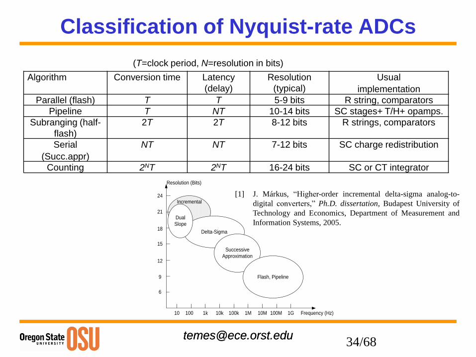
Classification of Nyquist-rate ADCs
Algorithm Conversion time Latency
(delay)
Resolution
(typical)
Usual
implementation
Parallel (flash) T T 5-9 bits R string, comparators
Pipeline T NT 10-14 bits SC stages+ T/H+ opamps.
Subranging (half-
flash)
2T 2T 8-12 bits R strings, comparators
Serial
(Succ.appr)
NT NT 7-12 bits SC charge redistribution
Counting 2NT 2NT 16-24 bits SC or CT integrator
(T=clock period, N=resolution in bits)
Delta-Sigma
Successive
Approximation
10 100 1k 10k 100k 1M 10M 100M 1G Frequency (Hz)
Resolution (Bits)
6
9
12
15
18
21
Flash, Pipeline
24
Dual
Slope
Incremental
[1] J. Márkus, “Higher-order incremental delta-sigma analog-to-
digital converters,” Ph.D. dissertation, Budapest University of
Technology and Economics, Department of Measurement and
Information Systems, 2005.
34/68
[email protected]@ece.orst.edu
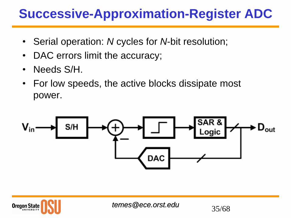
Successive-Approximation-Register ADC
• Serial operation: N cycles for N-bit resolution;
• DAC errors limit the accuracy;
• Needs S/H.
• For low speeds, the active blocks dissipate most
power.
35/68
[email protected]@ece.orst.edu
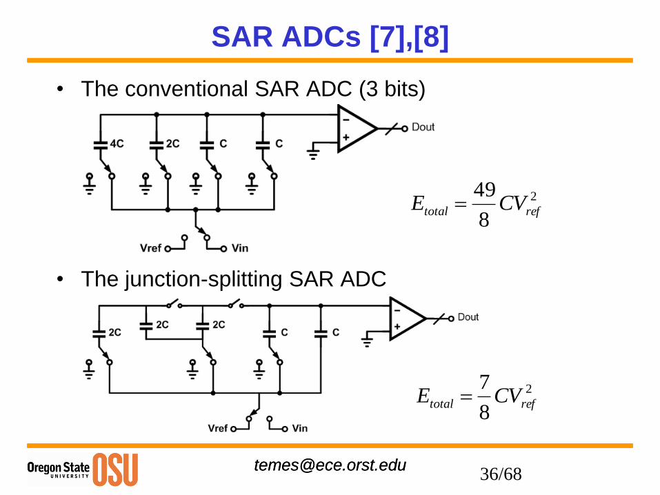
SAR ADCs [7],[8]
• The conventional SAR ADC (3 bits)
• The junction-splitting SAR ADC
2
8
49reftotal CVE
2
8
7reftotal CVE
36/68
[email protected]@ece.orst.edu
Energy Loss in SAR C Arrays
Energy loss considerations (for 3 bits):
• Energy required to charge an uncharged capacitor C
to voltage V is E = C.V2 . Half is lost in the switch.
• In SAR ADC, for Vin = 0, the initial step draws an
energy 2C.Vref2 Joules, subsequent steps draw
comparable amounts from Vref.
• In the modified array, the first step draws (C/2).Vref2,
the following ones less. The total energy is less than
C.Vref2. Mismatch effects may be worse.
37/68
[email protected]@ece.orst.edu
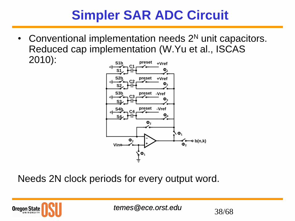
Simpler SAR ADC Circuit
• Conventional implementation needs 2N unit capacitors. Reduced cap implementation (W.Yu et al., ISCAS 2010):
Needs 2N clock periods for every output word.preset
Φ1
Φ2
Φ3
Φ4
...
...
...
...
...
1 2 3 4 N-1 N0
+Vref
+Vref
-Vref
-Vref
C1
C2
C3
C4
preset
preset
preset
preset
S1b
S2b
S3b
S4b
S1
S2
S3
S4
Vinb(n,k)
Φ2
Φ1
Φ2
Φ1
Φ2
Φ3
Φ4
Φ2
Φ1
(a)
(b)
38/68
[email protected]@ece.orst.edu
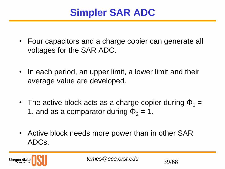
Simpler SAR ADC
• Four capacitors and a charge copier can generate all
voltages for the SAR ADC.
• In each period, an upper limit, a lower limit and their
average value are developed.
• The active block acts as a charge copier during Φ1 =
1, and as a comparator during Φ2 = 1.
• Active block needs more power than in other SAR
ADCs.
39/68
[email protected]@ece.orst.edu
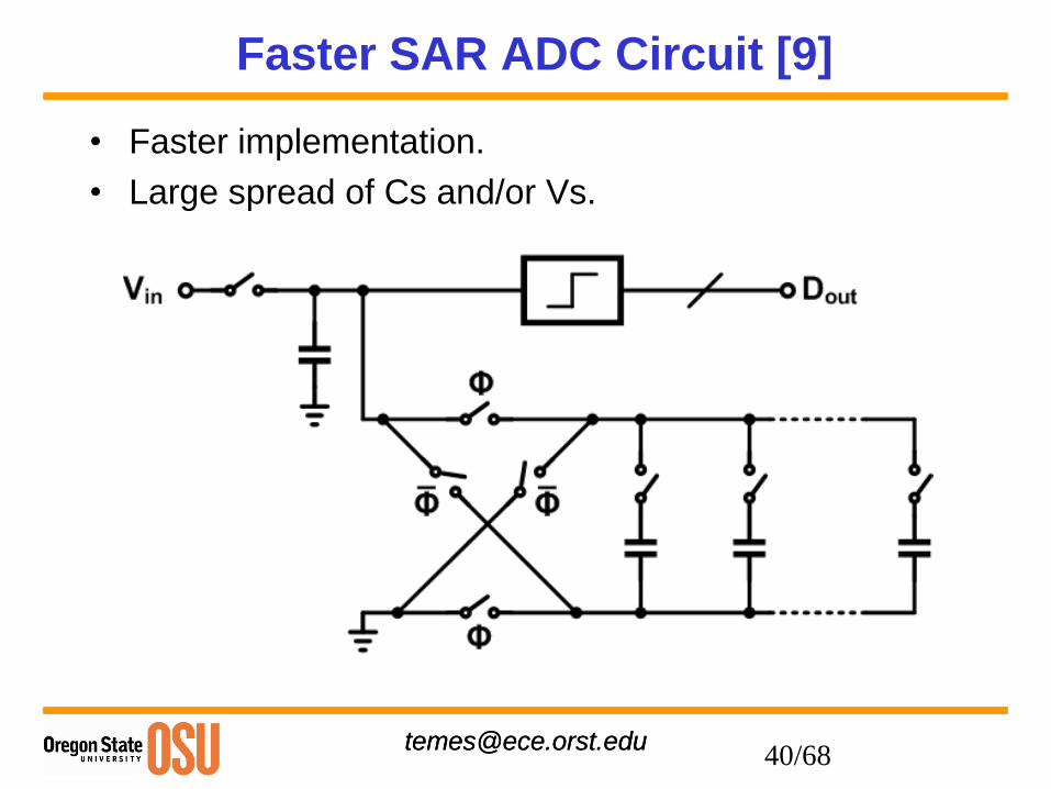
Faster SAR ADC Circuit [9]
• Faster implementation.
• Large spread of Cs and/or Vs.
40/68
[email protected]@ece.orst.edu
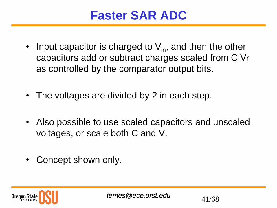
Faster SAR ADC
• Input capacitor is charged to Vin, and then the other
capacitors add or subtract charges scaled from C.Vr
as controlled by the comparator output bits.
• The voltages are divided by 2 in each step.
• Also possible to use scaled capacitors and unscaled
voltages, or scale both C and V.
• Concept shown only.
41/68
[email protected]@ece.orst.edu
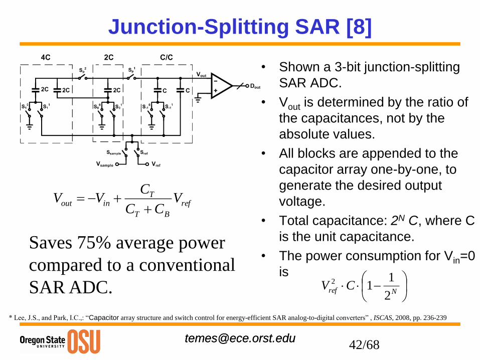
Junction-Splitting SAR [8]
• Shown a 3-bit junction-splitting
SAR ADC.
• Vout is determined by the ratio of
the capacitances, not by the
absolute values.
• All blocks are appended to the
capacitor array one-by-one, to
generate the desired output
voltage.
• Total capacitance: 2N·C, where C
is the unit capacitance.
• The power consumption for Vin=0
is
ref
BT
Tinout V
CC
CVV
Nref CV2
112
Saves 75% average power
compared to a conventional
SAR ADC.
* Lee, J.S., and Park, I.C.,: “Capacitor array structure and switch control for energy-efficient SAR analog-to-digital converters” , ISCAS, 2008, pp. 236-239
42/68
[email protected]@ece.orst.edu
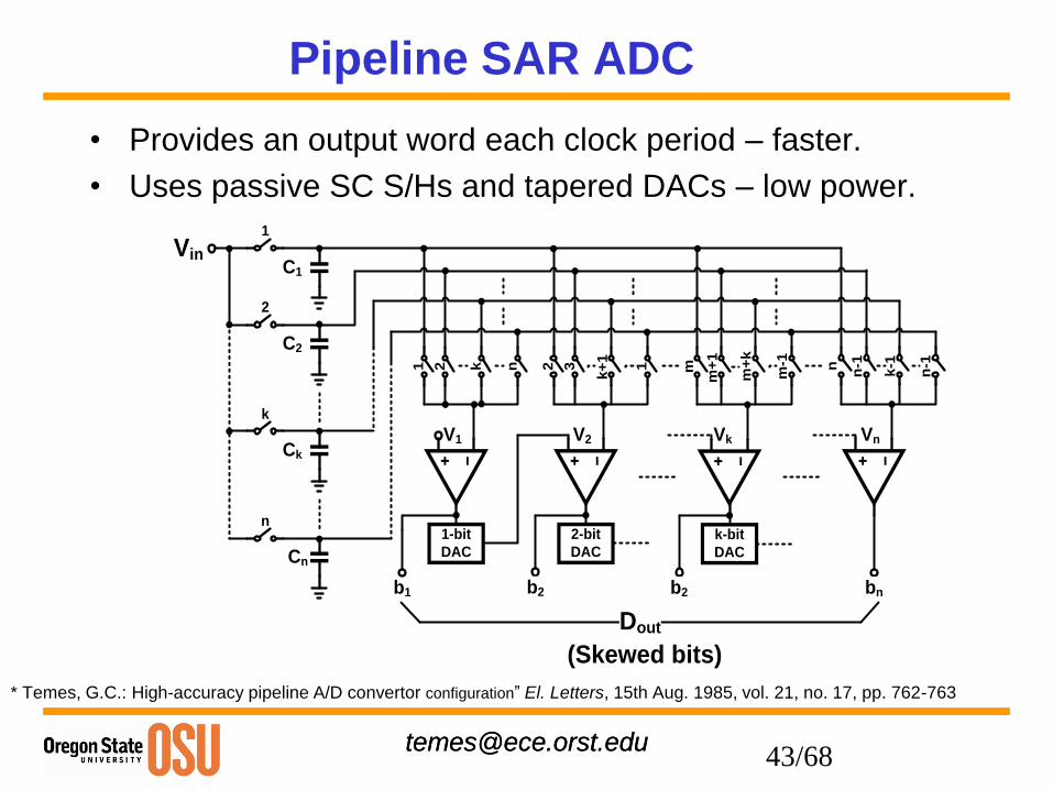
Pipeline SAR ADC
* Temes, G.C.: High-accuracy pipeline A/D convertor configuration” El. Letters, 15th Aug. 1985, vol. 21, no. 17, pp. 762-763
V1
Vin
1-bit
DAC
b1
V2
2-bit
DAC
b2
Vn
bn
C1
Ck
Cn
Dout
(Skewed bits)
C2
1
2
k
n
Vk
k-bit
DAC
b2
1 2 k n 2 3
k+
1
1 m
m+
1
m-1 n
n-1
k-1
n-1
m+
k
• Provides an output word each clock period – faster.
• Uses passive SC S/Hs and tapered DACs – low power.
43/68
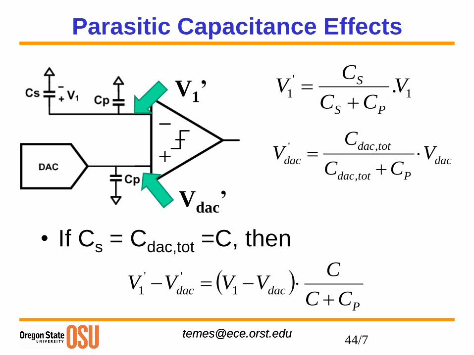
[email protected]@ece.orst.edu
• If Cs = Cdac,tot =C, then
44/7
V1’
Vdac’
1
'
1 .VCC
CV
PS
S
dac
Ptotdac
totdac
dac VCC
CV
,
,'
P
dacdacCC
CVVVV
1
''
1
Parasitic Capacitance Effects
[email protected]@ece.orst.edu
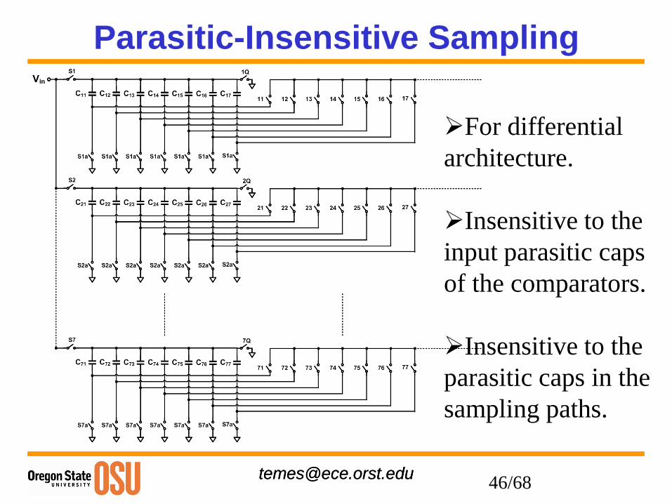
Parasitic-Insensitive Sampling
46/68
For differential
architecture.
Insensitive to the
input parasitic caps
of the comparators.
Insensitive to the
parasitic caps in the
sampling paths.
[email protected]@ece.orst.edu
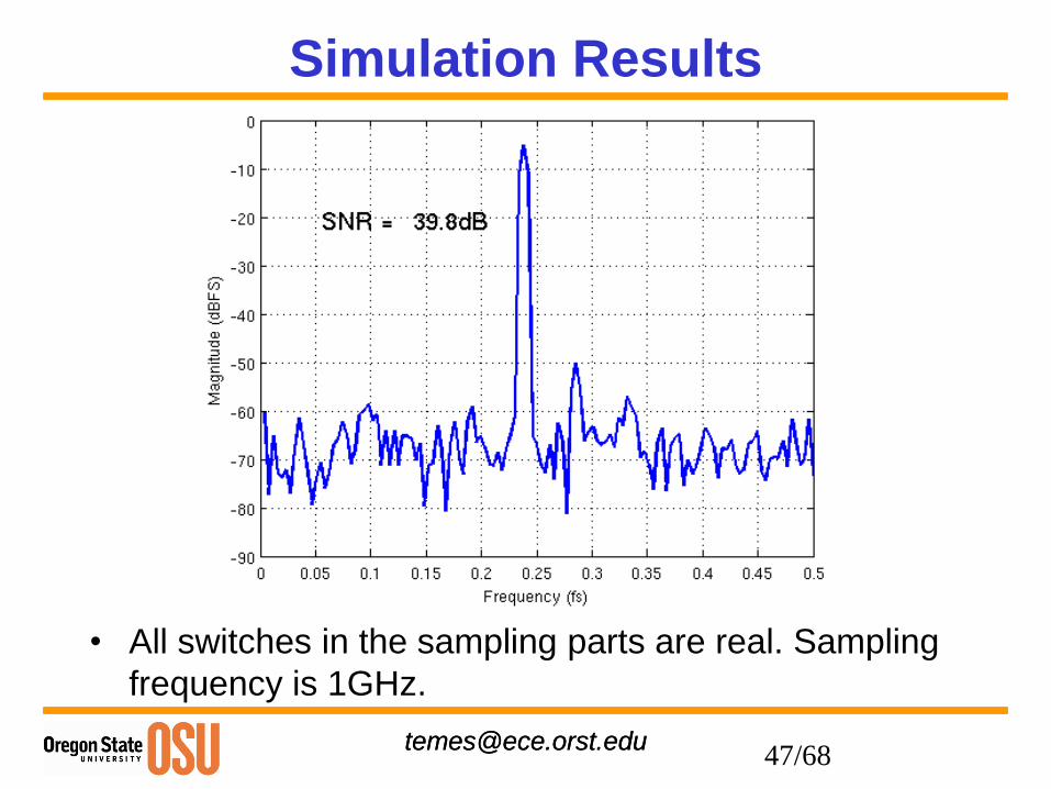
Simulation Results
• All switches in the sampling parts are real. Sampling
frequency is 1GHz.
47/68
[email protected]@ece.orst.edu
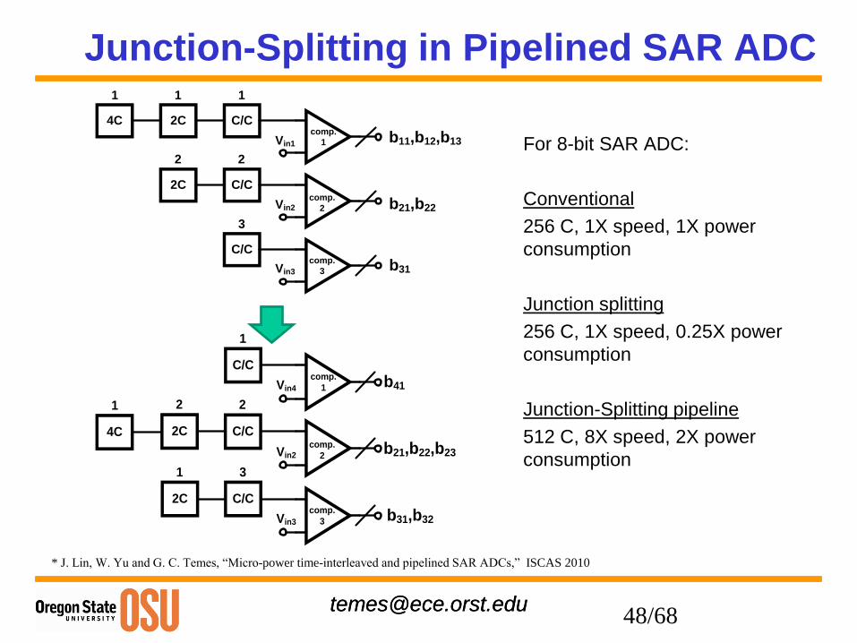
Junction-Splitting in Pipelined SAR ADC
For 8-bit SAR ADC:
Conventional
256 C, 1X speed, 1X power
consumption
Junction splitting
256 C, 1X speed, 0.25X power
consumption
Junction-Splitting pipeline
512 C, 8X speed, 2X power
consumption
comp.
1
comp.
2
comp.
3
C/C
C/C
C/C
2C4C
2C
1 1 1
22
3
Vin1
Vin2
Vin3
b11,b12,b13
b21,b22
b31
comp.
1
comp.
2
comp.
3
C/C
C/C
C/C
1
2
3
Vin4
Vin2
Vin3
b41
b21,b22,b23
b31,b32
2C
1
4C
1
2C
2
* J. Lin, W. Yu and G. C. Temes, “Micro-power time-interleaved and pipelined SAR ADCs,” ISCAS 2010
48/68
[email protected]@ece.orst.edu
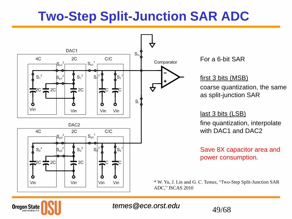
Two-Step Split-Junction SAR ADC
For a 6-bit SAR
first 3 bits (MSB)
coarse quantization, the same
as split-junction SAR
last 3 bits (LSB)
fine quantization, interpolate
with DAC1 and DAC2
Save 8X capacitor area and
power consumption.
* W. Yu, J. Lin and G. C. Temes, “Two-Step Split-Junction SAR
ADC,” ISCAS 2010
49/68
[email protected]@ece.orst.edu
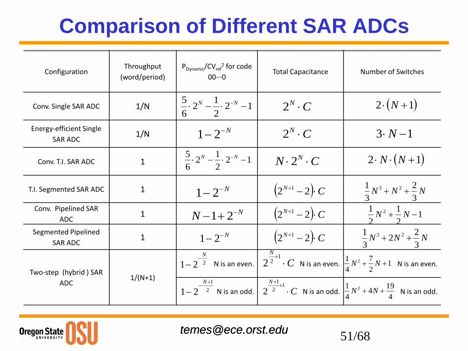
Comparison of Different SAR ADCs
ConfigurationThroughput
(word/period)
PDynamic/CVref2 for code
00∙∙∙0Total Capacitance Number of Switches
Conv. Single SAR ADC 1/N
Energy-efficient Single
SAR ADC1/N
Conv. T.I. SAR ADC 1
T.I. Segmented SAR ADC 1
Conv. Pipelined SAR
ADC1
Segmented Pipelined
SAR ADC1
Two-step (hybrid ) SAR
ADC1/(N+1)
N is an even. N is an even. N is an even.
N is an odd. N is an odd. N is an odd.
122
12
6
5 NN
CN 2 12 N
N 21 CN 2 13 N
122
12
6
5 NN
CN N 2 12 NN
N 21 CN 22 1 NNN3
2
3
1 23
NN 21 CN 22 1 12
1
2
1 2 NN
N 21 CN 22 1 NNN3
22
3
1 23
221
N
C
N
1
22 12
7
4
1 2 NN
2
1
21
N
C
N
1
2
1
24
194
4
1 2 NN
51/68

[email protected]@ece.orst.edu
[1] J. Márkus, “Higher-order incremental delta-sigma analog-to-
digital converters,” Ph.D. dissertation, Budapest University of
Technology and Economics, Department of Measurement and
Information Systems, 2005.
ADC Architectures
Delta-Sigma
Successive
Approximation
10 100 1k 10k 100k 1M 10M 100M 1G Frequency (Hz)
Resolution (Bits)
6
9
12
15
18
21
Flash, Pipeline
24
Dual
Slope
Incremental
52/68
[email protected]@ece.orst.edu
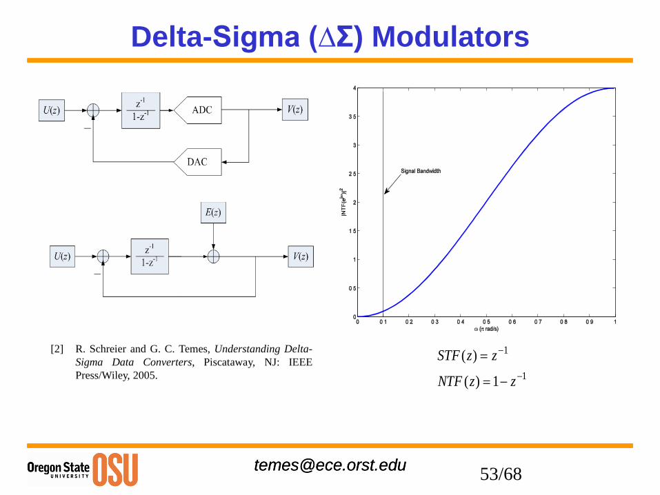
Delta-Sigma (∆Σ) Modulators
[2] R. Schreier and G. C. Temes, Understanding Delta-
Sigma Data Converters, Piscataway, NJ: IEEE
Press/Wiley, 2005. 1
1
1)(
)(
zzNTF
zzSTF
53/68
[email protected]@ece.orst.edu
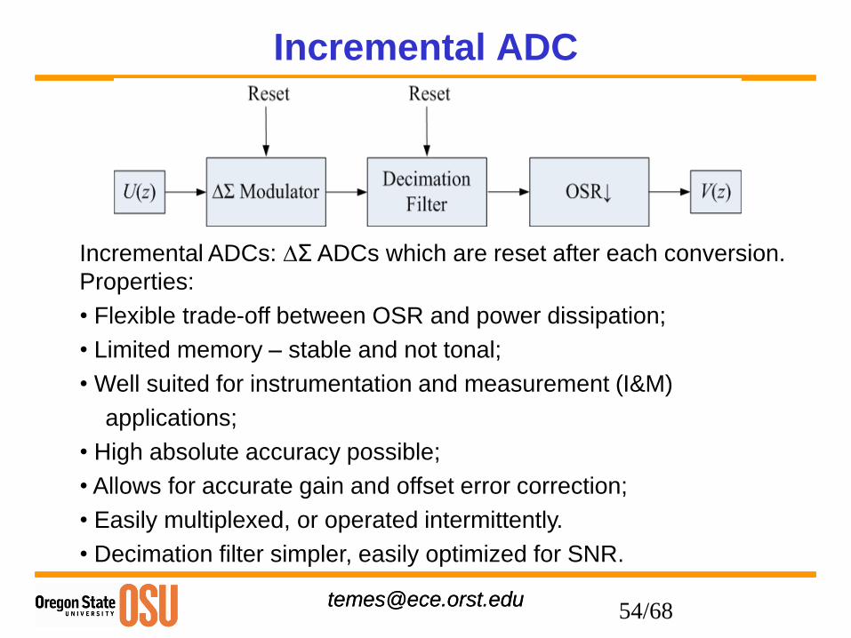
Incremental ADC
Incremental ADCs: ∆Σ ADCs which are reset after each conversion.
Properties:
• Flexible trade-off between OSR and power dissipation;
• Limited memory – stable and not tonal;
• Well suited for instrumentation and measurement (I&M)
applications;
• High absolute accuracy possible;
• Allows for accurate gain and offset error correction;
• Easily multiplexed, or operated intermittently.
• Decimation filter simpler, easily optimized for SNR.
54/68
[email protected]@ece.orst.edu
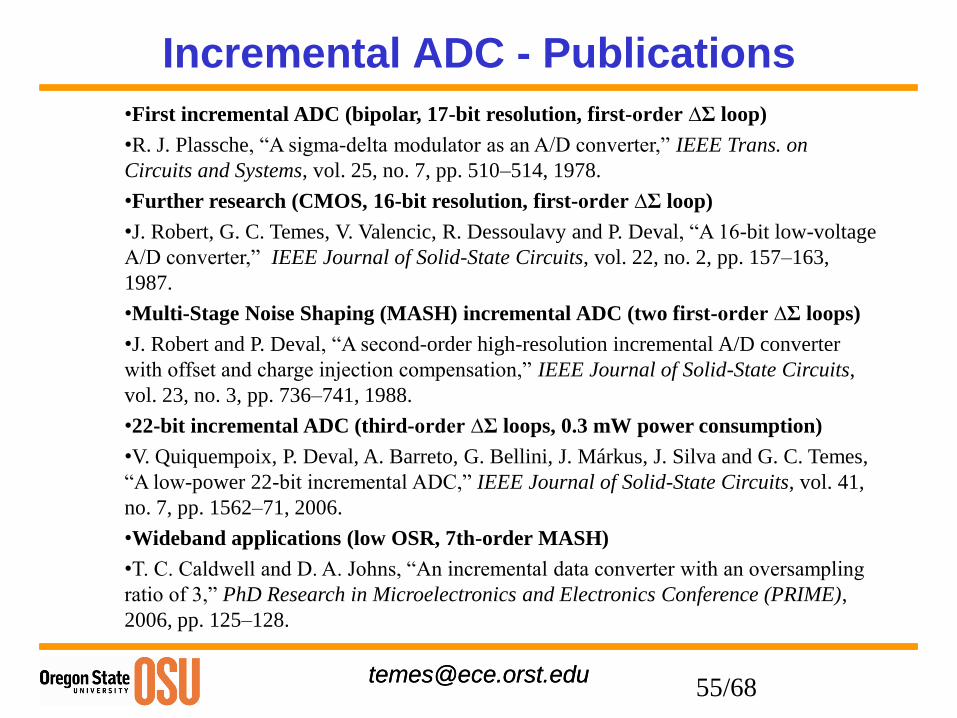
Incremental ADC - Publications
•First incremental ADC (bipolar, 17-bit resolution, first-order ∆Σ loop)
•R. J. Plassche, “A sigma-delta modulator as an A/D converter,” IEEE Trans. on
Circuits and Systems, vol. 25, no. 7, pp. 510–514, 1978.
•Further research (CMOS, 16-bit resolution, first-order ∆Σ loop)
•J. Robert, G. C. Temes, V. Valencic, R. Dessoulavy and P. Deval, “A 16-bit low-voltage
A/D converter,” IEEE Journal of Solid-State Circuits, vol. 22, no. 2, pp. 157–163,
1987.
•Multi-Stage Noise Shaping (MASH) incremental ADC (two first-order ∆Σ loops)
•J. Robert and P. Deval, “A second-order high-resolution incremental A/D converter
with offset and charge injection compensation,” IEEE Journal of Solid-State Circuits,
vol. 23, no. 3, pp. 736–741, 1988.
•22-bit incremental ADC (third-order ∆Σ loops, 0.3 mW power consumption)
•V. Quiquempoix, P. Deval, A. Barreto, G. Bellini, J. Márkus, J. Silva and G. C. Temes,
“A low-power 22-bit incremental ADC,” IEEE Journal of Solid-State Circuits, vol. 41,
no. 7, pp. 1562–71, 2006.
•Wideband applications (low OSR, 7th-order MASH)
•T. C. Caldwell and D. A. Johns, “An incremental data converter with an oversampling
ratio of 3,” PhD Research in Microelectronics and Electronics Conference (PRIME),
2006, pp. 125–128.
55/68
[email protected]@ece.orst.edu
Incremental ADC – Commercial ADCs
Sometimes referred to as charge-balancing ∆Σ ADCs, one-shot ∆Σ
ADCs or no-latency ∆Σ ADCs.
• AD77xx product family, Analog Devices
16-bit ~ 24-bit resolution, 1~10 channels, 60~2.5M SPS
• ADS124x product family, Burr-Brown (Texas Instruments)
24-bit resolution, 4~8 channels, 15 SPS
• CS55xx product family, Cirrus Logic
24-bit resolution, 6.25~3840 SPS
• LTC24xx product family, Linear Technology
16-bit ~ 24-bit resolution, 1~16 channels, 6.9~8000 SPS
56/68
[email protected]@ece.orst.edu
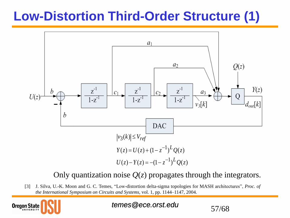
Low-Distortion Third-Order Structure (1)
)()1()()(
)()1()()(
)(
1
1
3
zQzzYzU
zQzzUzY
Vkv
L
L
ref
Only quantization noise Q(z) propagates through the integrators.
[3] J. Silva, U.-K. Moon and G. C. Temes, “Low-distortion delta-sigma topologies for MASH architectures”, Proc. of
the International Symposium on Circuits and Systems, vol. 1, pp. 1144–1147, 2004.
57/68
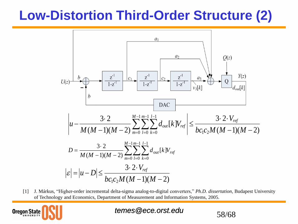
[email protected]@ece.orst.edu
Low-Distortion Third-Order Structure (2)
1 1 1
1 20 0 0
3 23 2[ ]
( 1)( 2) ( 1)( 2)
M m lref
out ref
m l k
Vu d k V
M M M bc c M M M
1
0
1
0
1
0
][)2)(1(
23M
m
m
l
l
k
refout VkdMMM
D
1 2
3 2
( 1)( 2)
refVu D
bc c M M M
[1] J. Márkus, “Higher-order incremental delta-sigma analog-to-digital converters,” Ph.D. dissertation, Budapest University
of Technology and Economics, Department of Measurement and Information Systems, 2005.
58/68
[email protected]@ece.orst.edu
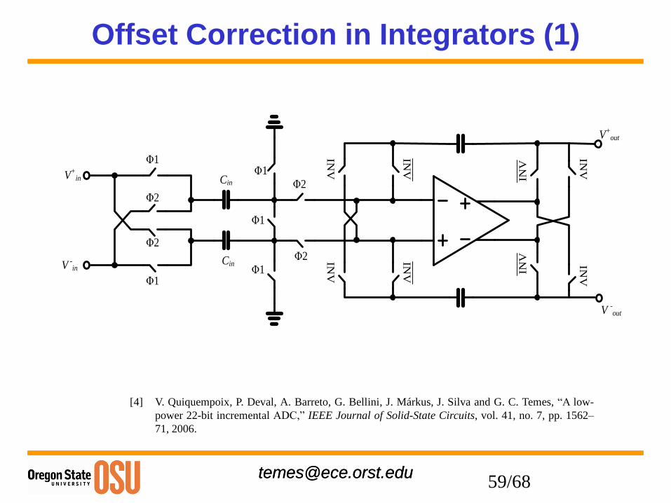
Offset Correction in Integrators (1)
[4] V. Quiquempoix, P. Deval, A. Barreto, G. Bellini, J. Márkus, J. Silva and G. C. Temes, “A low-
power 22-bit incremental ADC,” IEEE Journal of Solid-State Circuits, vol. 41, no. 7, pp. 1562–
71, 2006.
INV
INV
INV
INV
INV
INV
INV
INV
Φ2
Φ2
Φ1
Φ1
Φ1
Cin
Cin
Φ1
Φ1
Φ2
Φ2
V+in
V -in
V+out
V -out
59/68
[email protected]@ece.orst.edu
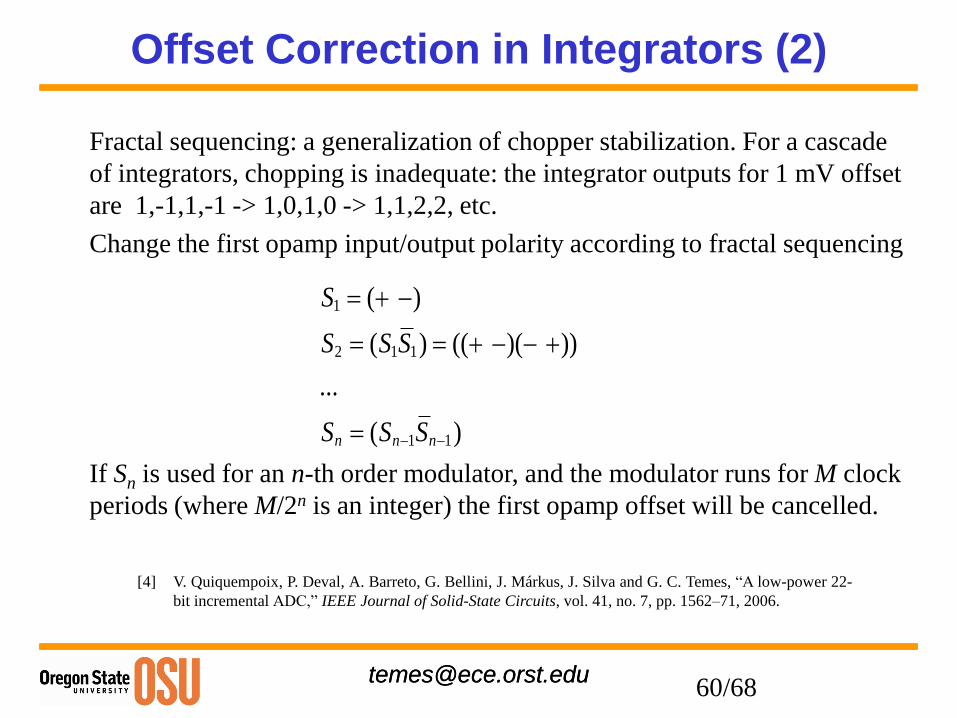
Offset Correction in Integrators (2)
Fractal sequencing: a generalization of chopper stabilization. For a cascade
of integrators, chopping is inadequate: the integrator outputs for 1 mV offset
are 1,-1,1,-1 -> 1,0,1,0 -> 1,1,2,2, etc.
Change the first opamp input/output polarity according to fractal sequencing
If Sn is used for an n-th order modulator, and the modulator runs for M clock
periods (where M/2n is an integer) the first opamp offset will be cancelled.
[4] V. Quiquempoix, P. Deval, A. Barreto, G. Bellini, J. Márkus, J. Silva and G. C. Temes, “A low-power 22-
bit incremental ADC,” IEEE Journal of Solid-State Circuits, vol. 41, no. 7, pp. 1562–71, 2006.
1
2 1 1
1 1
( )
( ) (( )( ))
...
( )n n n
S
S S S
S S S
60/68
[email protected]@ece.orst.edu
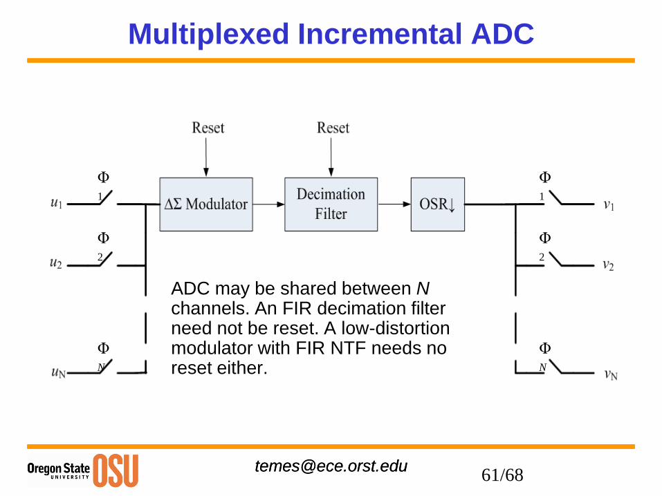
Multiplexed Incremental ADC
ADC may be shared between Nchannels. An FIR decimation filter need not be reset. A low-distortion modulator with FIR NTF needs no reset either.
Φ1
Φ2
ΦN
Φ1
Φ2
ΦN
61/68
[email protected]@ece.orst.edu
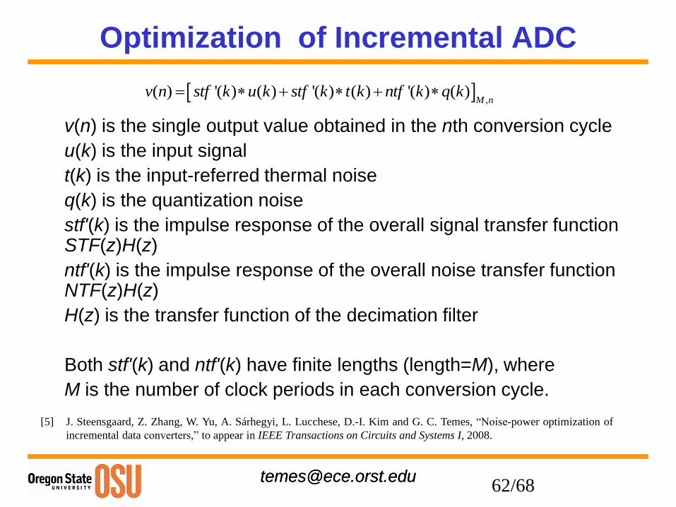
Optimization of Incremental ADC
v(n) is the single output value obtained in the nth conversion cycle
u(k) is the input signal
t(k) is the input-referred thermal noise
q(k) is the quantization noise
stf'(k) is the impulse response of the overall signal transfer function STF(z)H(z)
ntf'(k) is the impulse response of the overall noise transfer function NTF(z)H(z)
H(z) is the transfer function of the decimation filter
Both stf'(k) and ntf'(k) have finite lengths (length=M), where
M is the number of clock periods in each conversion cycle.
,
( ) '( ) ( ) '( ) ( ) '( ) ( )M n
v n stf k u k stf k t k ntf k q k
[5] J. Steensgaard, Z. Zhang, W. Yu, A. Sárhegyi, L. Lucchese, D.-I. Kim and G. C. Temes, “Noise-power optimization of
incremental data converters,” to appear in IEEE Transactions on Circuits and Systems I, 2008.
62/68
[email protected]@ece.orst.edu
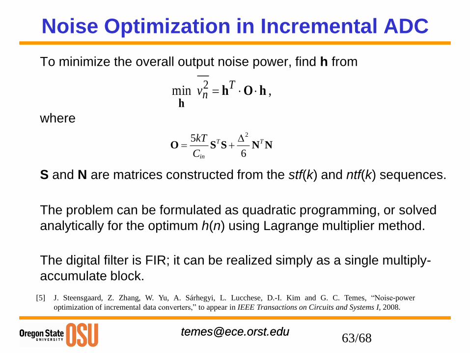
Noise Optimization in Incremental ADC
To minimize the overall output noise power, find h from
where
S and N are matrices constructed from the stf(k) and ntf(k) sequences.
The problem can be formulated as quadratic programming, or solved
analytically for the optimum h(n) using Lagrange multiplier method.
The digital filter is FIR; it can be realized simply as a single multiply-
accumulate block.
25
6
T T
in
kT
C
O S S N N
[5] J. Steensgaard, Z. Zhang, W. Yu, A. Sárhegyi, L. Lucchese, D.-I. Kim and G. C. Temes, “Noise-power
optimization of incremental data converters,” to appear in IEEE Transactions on Circuits and Systems I, 2008.
, min 2hOh
h T
nv
63/68
[email protected]@ece.orst.edu
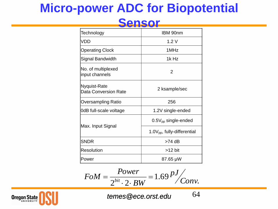
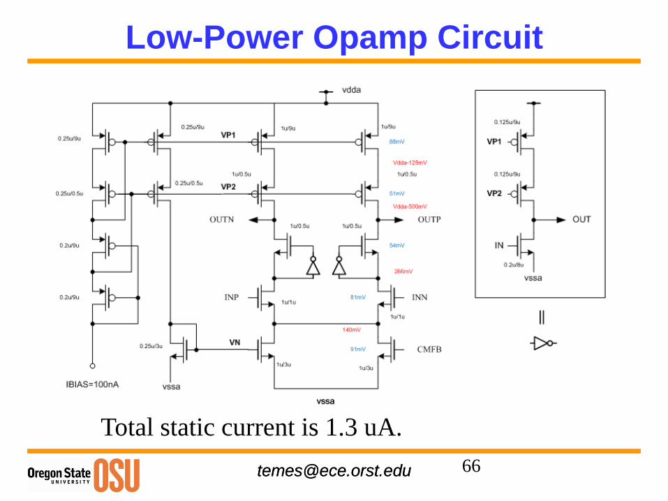
Micro-power ADC for Biopotential
Sensor
64
.69.1
22 ConvpJ
BW
PowerFoM
bit
Technology IBM 90nm
VDD 1.2 V
Operating Clock 1MHz
Signal Bandwidth 1k Hz
No. of multiplexed
input channels2
Nyquist-Rate
Data Conversion Rate2 ksample/sec
Oversampling Ratio 256
0dB full-scale voltage 1.2V single-ended
Max. Input Signal
0.5Vpp single-ended
1.0Vpp, fully-differential
SNDR >74 dB
Resolution >12 bit
Power 87.65 μW
[email protected]@ece.orst.edu
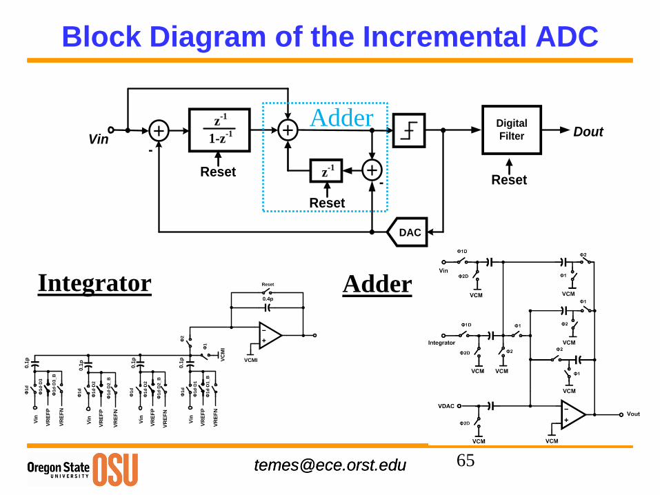
Block Diagram of the Incremental ADC
65
Reset
DAC
-
-
Reset
Vin
z-1
1-z-1
z-1
Digital
Filter Dout
Reset
VCMI
VR
EF
P
VR
EF
N
Vin
Φ1
d
VR
EF
P
VR
EF
N
Vin
Φ1
d
Φ2
VC
MIΦ
1V
RE
FP
VR
EF
N
Vin
Φ1
d
VR
EF
P
VR
EF
N
Vin
Φ1d
Reset
0.1
p
0.1
p
0.1
p
0.1
p
0.4p
Φ1
d·D
3
Φ1
d·D
3_
B
Φ1
d·D
2
Φ1
d·D
2_
B
Φ1
d·D
2
Φ1
d·D
1
Φ1
d·D
1_
B
Φ1
d·D
2_
B
Integrator Adder
Adder
[email protected]@ece.orst.edu
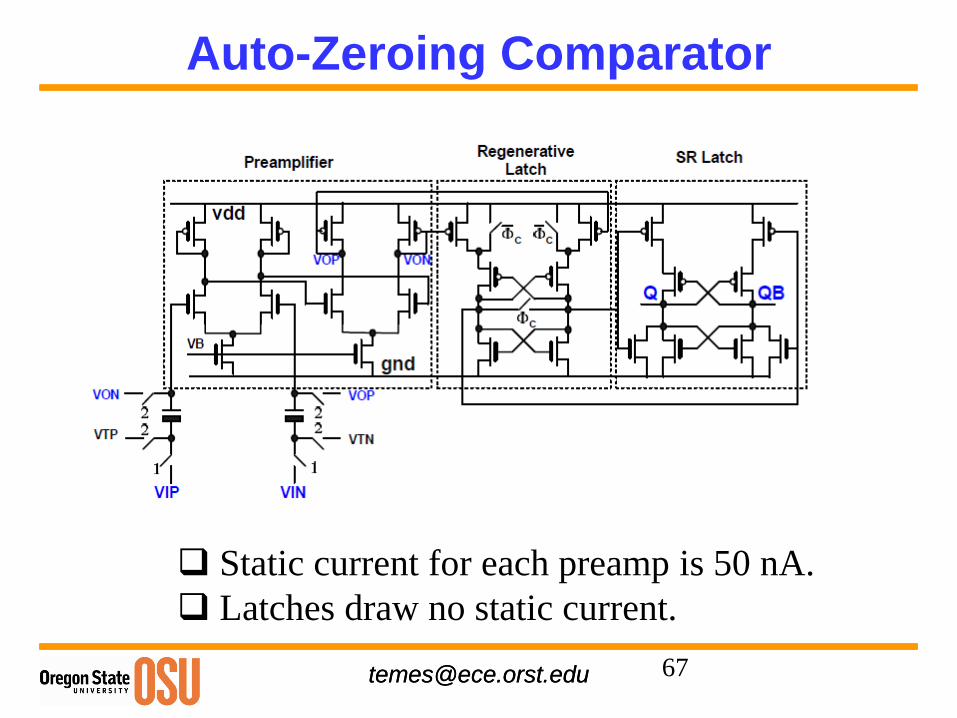
Auto-Zeroing Comparator
67
Static current for each preamp is 50 nA.
Latches draw no static current.
[email protected]@ece.orst.edu
Simulated PSD of ΔΣ Modulator
68
102
103
104
105
-140
-120
-100
-80
-60
-40
-20
0PSD of Noise-Coupling Sigma-Delta Modulator
Frequency [Hz]
PS
D [
dB
]
SNR = 85.1dB @ OSR= 256
Conditions
• IBM 90nm Technology
• Sampling clock :1.024MHz
• OSR: 256
• Signal frequency: 375 Hz
• Single-ended amplitude: Vpp=0.5V
• Fully-differential ampl.: Vpp=1.0V
SNDR = 85.1 dB
ADC in incremental mode is being
simulated now.
Simulated FoM
./69.1222
65.87
22 14convpJ
kHz
W
BW
Powerbit
[email protected]@ece.orst.edu
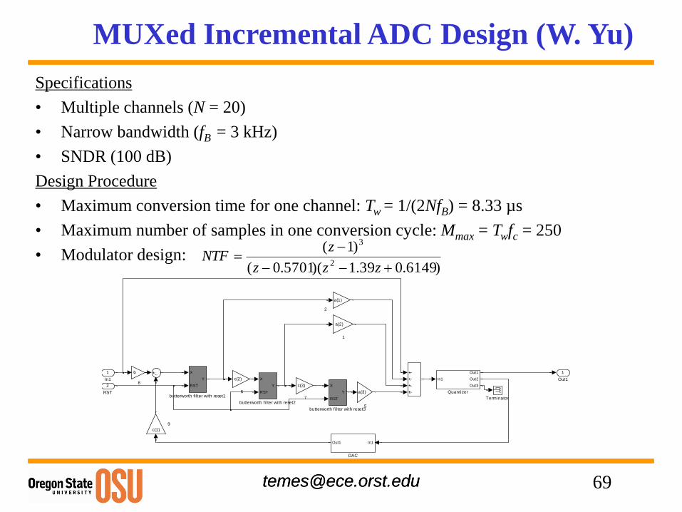
MUXed Incremental ADC Design (W. Yu)
Specifications
• Multiple channels (N = 20)
• Narrow bandwidth (fB = 3 kHz)
• SNDR (100 dB)
Design Procedure
• Maximum conversion time for one channel: Tw = 1/(2NfB) = 8.33 µs
• Maximum number of samples in one conversion cycle: Mmax = Twfc = 250
• Modulator design:)6149.039.1)(5701.0(
)1(2
3
zzz
zNTF
2
1
Out1
X
RST
Y
butterworth fi lter with reset3
X
RST
Y
butterworth fi lter with reset2
X
RST
Y
butterworth fi lter with reset1Terminator
In1
Out1
Out2
Out3
Quantizer
In1Out1
DAC
c(1)
9
b
8c(3)
7
c(2)
6 a(3)
5
a(2)
1
a(1)
2
RST
1
In1
69
[email protected]@ece.orst.edu
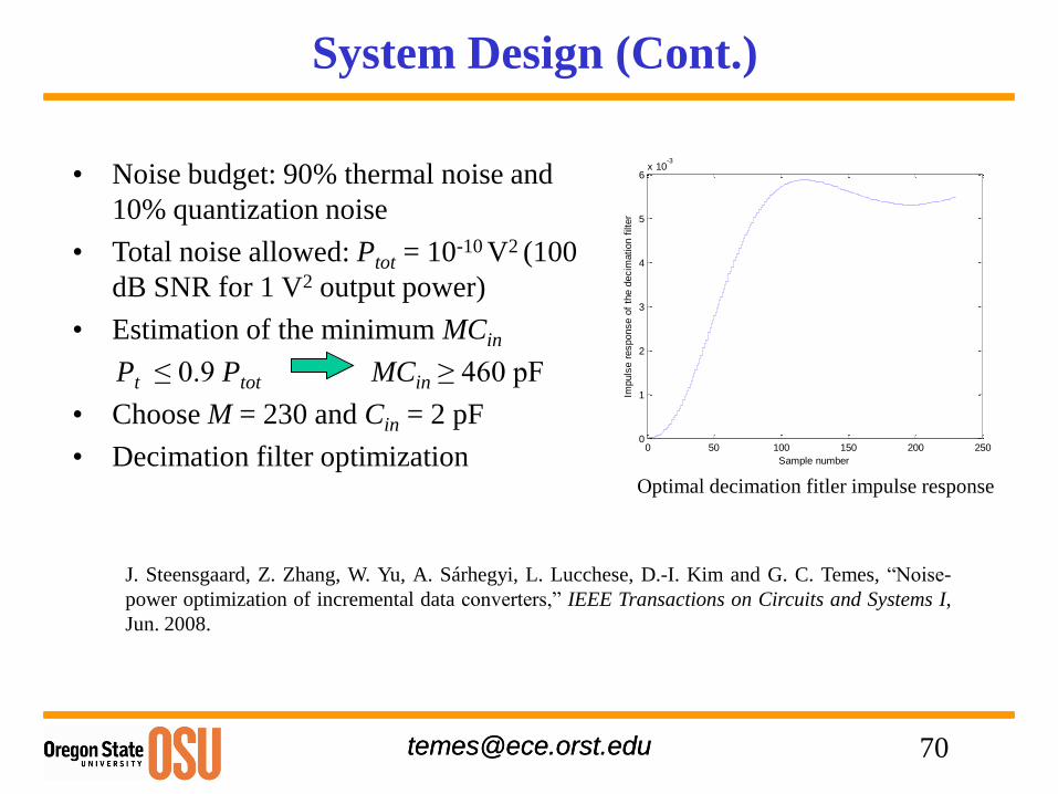
System Design (Cont.)
• Noise budget: 90% thermal noise and
10% quantization noise
• Total noise allowed: Ptot = 10-10 V2 (100
dB SNR for 1 V2 output power)
• Estimation of the minimum MCin
Pt ≤ 0.9 Ptot MCin ≥ 460 pF
• Choose M = 230 and Cin = 2 pF
• Decimation filter optimization0 50 100 150 200 250
0
1
2
3
4
5
6x 10
-3
Sample number
Impuls
e r
esponse o
f th
e d
ecim
ation f
ilter
J. Steensgaard, Z. Zhang, W. Yu, A. Sárhegyi, L. Lucchese, D.-I. Kim and G. C. Temes, “Noise-
power optimization of incremental data converters,” IEEE Transactions on Circuits and Systems I,
Jun. 2008.
Optimal decimation fitler impulse response
70
[email protected]@ece.orst.edu
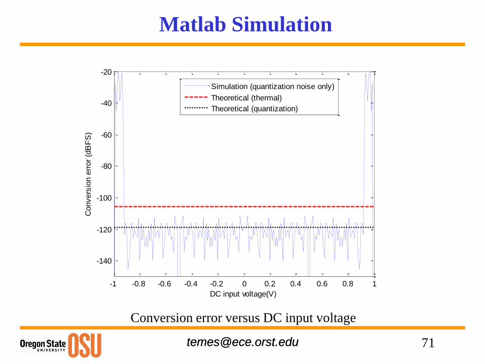
Matlab Simulation
Conversion error versus DC input voltage
-1 -0.8 -0.6 -0.4 -0.2 0 0.2 0.4 0.6 0.8 1
-140
-120
-100
-80
-60
-40
-20
DC input voltage(V)
Convers
ion e
rror
(dB
FS
)Simulation (quantization noise only)
Theoretical (thermal)
Theoretical (quantization)
71
[email protected]@ece.orst.edu
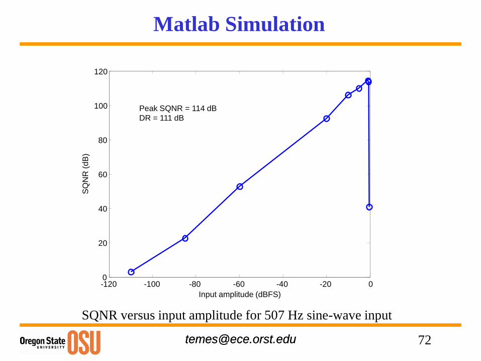
Matlab Simulation
SQNR versus input amplitude for 507 Hz sine-wave input
-120 -100 -80 -60 -40 -20 00
20
40
60
80
100
120
Input amplitude (dBFS)
SQ
NR
(dB
)
Peak SQNR = 114 dB
DR = 111 dB
72
[email protected]@ece.orst.edu
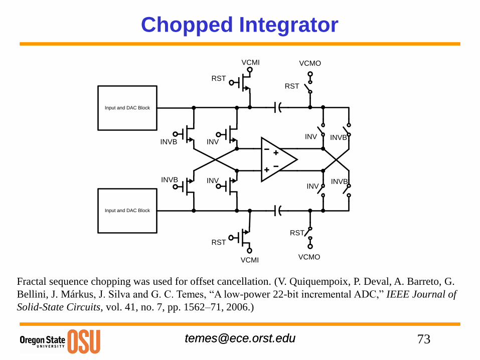
Chopped Integrator
Fractal sequence chopping was used for offset cancellation. (V. Quiquempoix, P. Deval, A. Barreto, G.
Bellini, J. Márkus, J. Silva and G. C. Temes, “A low-power 22-bit incremental ADC,” IEEE Journal of
Solid-State Circuits, vol. 41, no. 7, pp. 1562–71, 2006.)
Input and DAC Block
Input and DAC Block
INVB
INVB
INVB
INVB
INV
INV
INV
INV
RST
RST
RST
RST
VCMI VCMO
VCMI VCMO
73
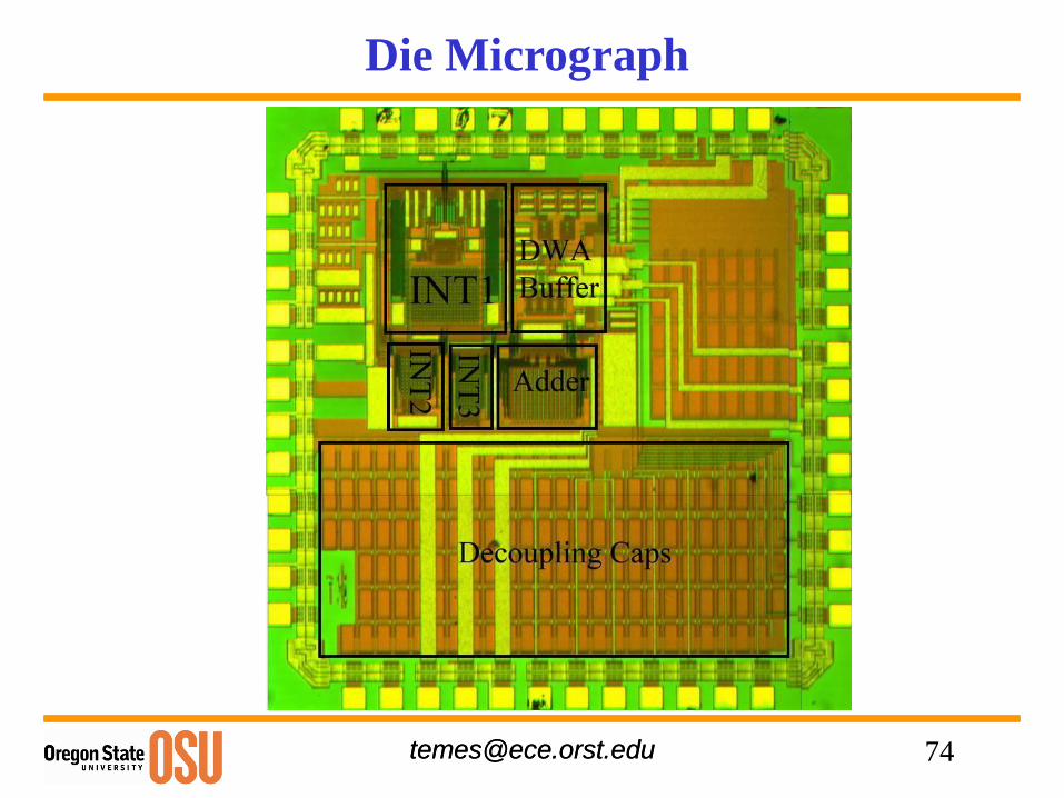
[email protected]@ece.orst.edu
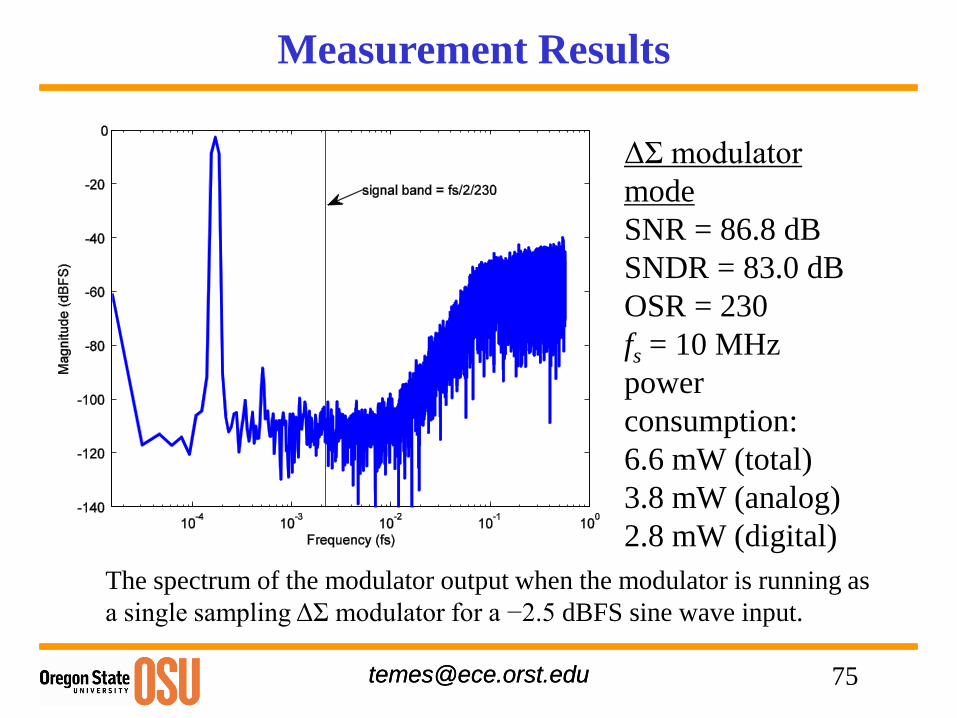
Measurement Results
The spectrum of the modulator output when the modulator is running as
a single sampling ΔΣ modulator for a −2.5 dBFS sine wave input.
ΔΣ modulator
mode
SNR = 86.8 dB
SNDR = 83.0 dB
OSR = 230
fs = 10 MHz
power
consumption:
6.6 mW (total)
3.8 mW (analog)
2.8 mW (digital)
75
[email protected]@ece.orst.edu
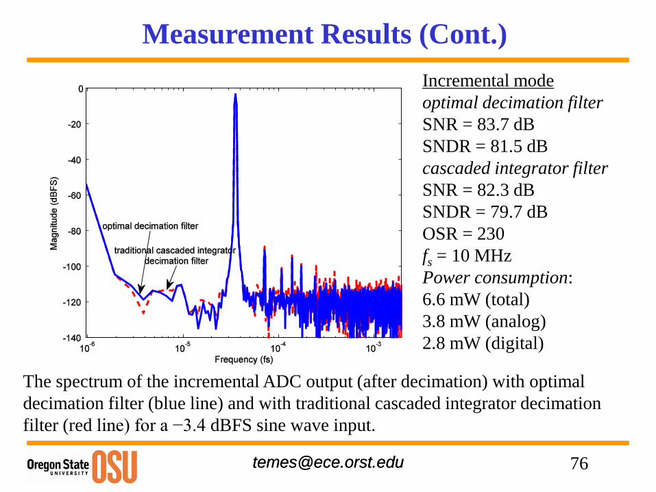
Measurement Results (Cont.)
The spectrum of the incremental ADC output (after decimation) with optimal
decimation filter (blue line) and with traditional cascaded integrator decimation
filter (red line) for a −3.4 dBFS sine wave input.
Incremental mode
optimal decimation filter
SNR = 83.7 dB
SNDR = 81.5 dB
cascaded integrator filter
SNR = 82.3 dB
SNDR = 79.7 dB
OSR = 230
fs = 10 MHz
Power consumption:
6.6 mW (total)
3.8 mW (analog)
2.8 mW (digital)
76
[email protected]@ece.orst.edu
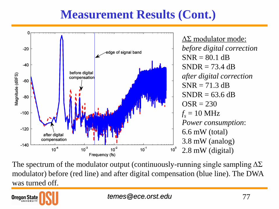
Measurement Results (Cont.)
The spectrum of the modulator output (continuously-running single sampling ΔΣ
modulator) before (red line) and after digital compensation (blue line). The DWA
was turned off.
ΔΣ modulator mode:
before digital correction
SNR = 80.1 dB
SNDR = 73.4 dB
after digital correction
SNR = 71.3 dB
SNDR = 63.6 dB
OSR = 230
fs = 10 MHz
Power consumption:
6.6 mW (total)
3.8 mW (analog)
2.8 mW (digital)
77
[email protected]@ece.orst.edu
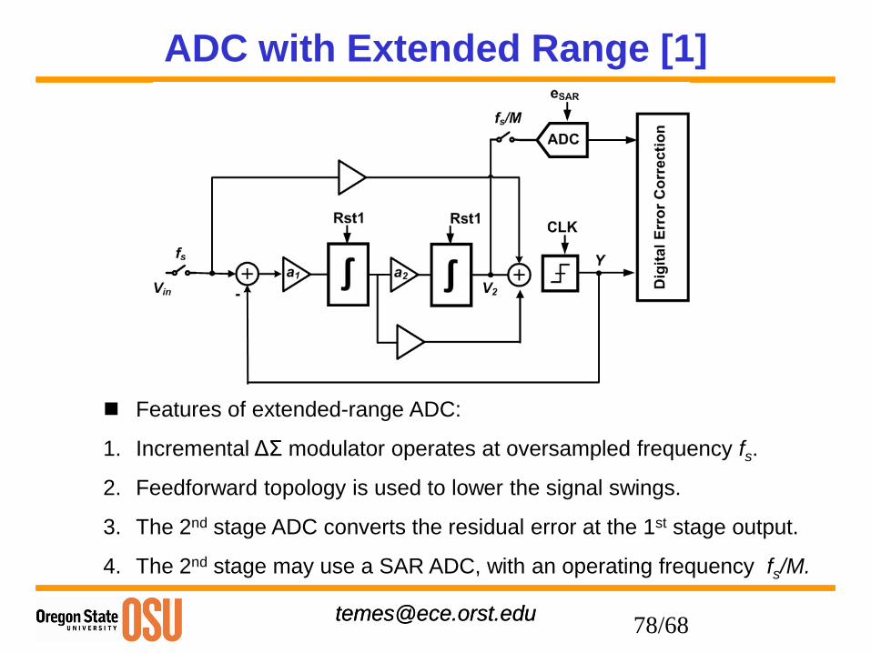
ADC with Extended Range [1]
Features of extended-range ADC:
1. Incremental ΔΣ modulator operates at oversampled frequency fs.
2. Feedforward topology is used to lower the signal swings.
3. The 2nd stage ADC converts the residual error at the 1st stage output.
4. The 2nd stage may use a SAR ADC, with an operating frequency fs/M.
78/68
[email protected]@ece.orst.edu
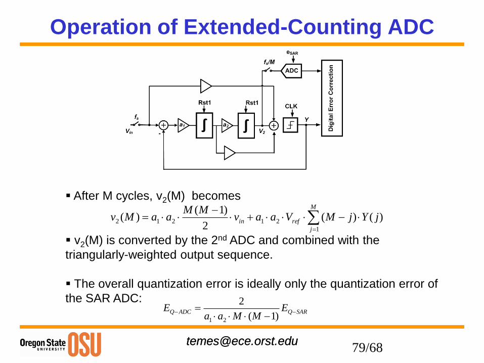
Operation of Extended-Counting ADC
After M cycles, v2(M) becomes
)()(2
)1()(
1
21212 jYjMVaavMM
aaMvM
j
refin
v2(M) is converted by the 2nd ADC and combined with the
triangularly-weighted output sequence.
The overall quantization error is ideally only the quantization error of
the SAR ADC: SARQADCQ E
MMaaE
)1(
2
21
79/68
[email protected]@ece.orst.edu
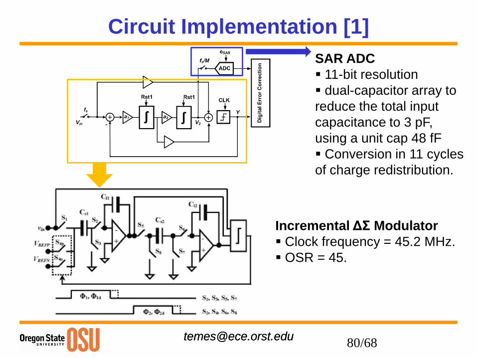
Circuit Implementation [1]
Incremental ΔΣ Modulator
Clock frequency = 45.2 MHz.
OSR = 45.
SAR ADC
11-bit resolution
dual-capacitor array to
reduce the total input
capacitance to 3 pF,
using a unit cap 48 fF
Conversion in 11 cycles
of charge redistribution.
80/68
[email protected]@ece.orst.edu
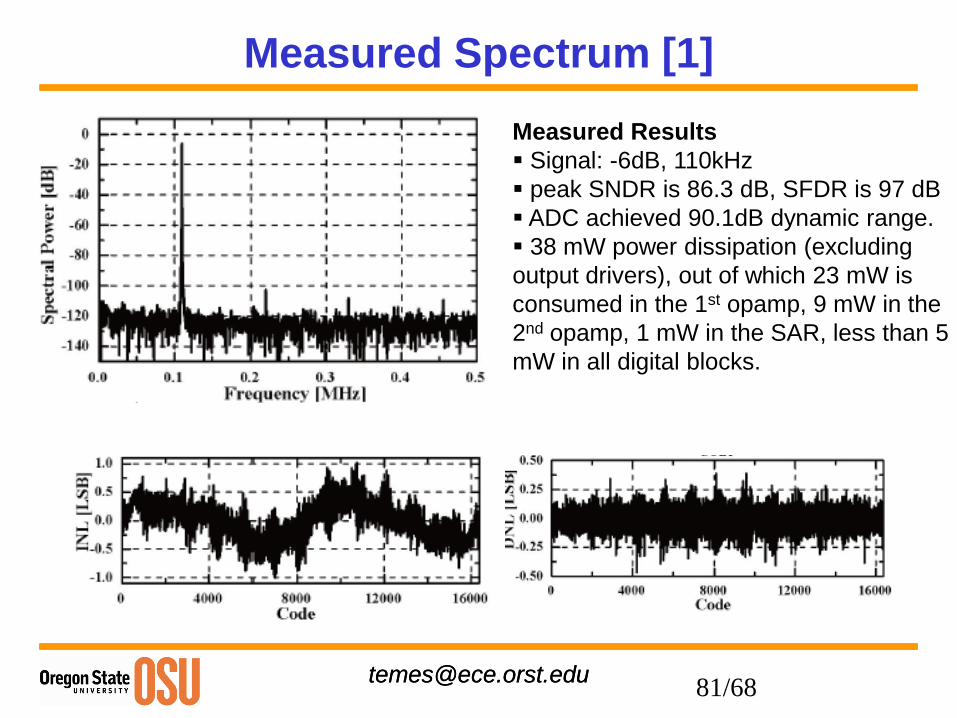
Measured Spectrum [1]
Measured Results
Signal: -6dB, 110kHz
peak SNDR is 86.3 dB, SFDR is 97 dB
ADC achieved 90.1dB dynamic range.
38 mW power dissipation (excluding
output drivers), out of which 23 mW is
consumed in the 1st opamp, 9 mW in the
2nd opamp, 1 mW in the SAR, less than 5
mW in all digital blocks.
81/68
[email protected]@ece.orst.edu
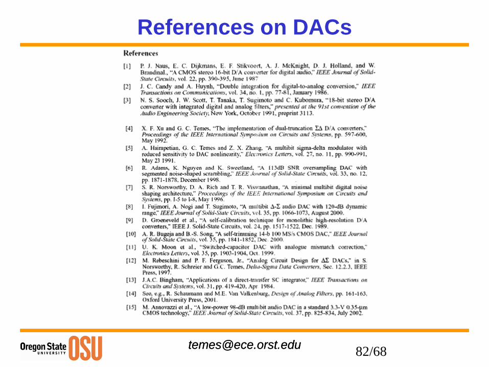
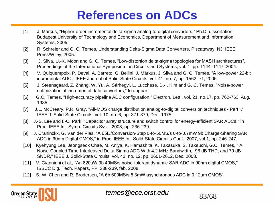
References on ADCs[1] J. Márkus, “Higher-order incremental delta-sigma analog-to-digital converters,” Ph.D. dissertation,
Budapest University of Technology and Economics, Department of Measurement and Information
Systems, 2005.
[2] R. Schreier and G. C. Temes, Understanding Delta-Sigma Data Converters, Piscataway, NJ: IEEE
Press/Wiley, 2005.
[3] J. Silva, U.-K. Moon and G. C. Temes, “Low-distortion delta-sigma topologies for MASH architectures”,
Proceedings of the International Symposium on Circuits and Systems, vol. 1, pp. 1144–1147, 2004.
[4] V. Quiquempoix, P. Deval, A. Barreto, G. Bellini, J. Márkus, J. Silva and G. C. Temes, “A low-power 22-bit
incremental ADC,” IEEE Journal of Solid-State Circuits, vol. 41, no. 7, pp. 1562–71, 2006.
[5] J. Steensgaard, Z. Zhang, W. Yu, A. Sárhegyi, L. Lucchese, D.-I. Kim and G. C. Temes, “Noise-power
optimization of incremental data converters,” to appear.
[6] G.C. Temes, "High-accuracy pipeline ADC configuration," Electron. Lett., vol. 21, no.17, pp. 762-763, Aug.
1985
[7] J.L. McCreary, P.R. Gray, "All-MOS charge distribution analog-to-digital conversion techniques - Part I,"
IEEE J. Solid-State Circuits, vol. 10, no. 6, pp. 371-379, Dec. 1975.
[8] J.-S. Lee and I.-C. Park, "Capacitor array structure and switch control for energy-efficient SAR ADCs," in
Proc. IEEE Int. Symp. Circuits Syst., 2008, pp. 236-239.
[9] J. Craninckx, G. Van der Plas, “A 65fJ/Conversion-Step 0-to-50MS/s 0-to-0.7mW 9b Charge-Sharing SAR
ADC in 90nm Digital CMOS,” in Proc. IEEE Int. Solid-State Circuits Conf., 2007, vol.1, pp. 246-247.
[10] Kyehyung Lee, Jeongseok Chae, M. Aniya, K. Hamashita, K. Takasuka, S. Takeuchi, G.C. Temes, " A
Noise-Coupled Time-Interleaved Delta-Sigma ADC With 4.2 MHz Bandwidth, -98 dB THD, and 79 dB
SNDR," IEEE J. Solid-State Circuits, vol. 43, no. 12, pp. 2601-2612, Dec. 2008.
[11] V. Gianninni et al., “An 820uW 9b 40MS/s noise-tolerant dynamic-SAR ADC in 90nm digital CMOS,”
ISSCC Dig. Tech. Papers, PP. 238-239, feb. 2008
[12] S.-W. Chen and R. Brodersen, “A 6b 600MS/s 5.3mW asynchronous ADC in 0.12um CMOS”
83/68
[email protected]@ece.orst.edu
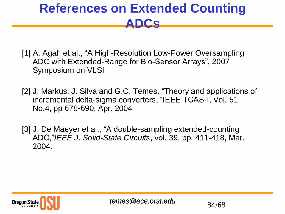
References on Extended Counting
ADCs
[1] A. Agah et al., “A High-Resolution Low-Power Oversampling ADC with Extended-Range for Bio-Sensor Arrays”, 2007 Symposium on VLSI
[2] J. Markus, J. Silva and G.C. Temes, “Theory and applications of incremental delta-sigma converters, “IEEE TCAS-I, Vol. 51, No.4, pp 678-690, Apr. 2004
[3] J. De Maeyer et al., “A double-sampling extended-counting ADC,”IEEE J. Solid-State Circuits, vol. 39, pp. 411-418, Mar. 2004.
84/68