microcontroller-based current-mode control for …
TRANSCRIPT

MICROCONTROLLER-BASED CURRENT-MODE CONTROL
FOR POWER CONVERTERS
Except where reference is made to the work of others, the work described in this dissertation is my own or was done in collaboration with my advisory committee. This dissertation does not
include proprietary or classified information.
________________________________________ Dake He
Certificate of Approval:
_________________________________ Michael E. Greene Professor Electrical and Computer Engineering _________________________________ John Y. Hung Associate Professor Electrical and Computer Engineering
_________________________________ R. Mark Nelms, Chair Professor Electrical and Computer Engineering _________________________________ Stephen L. McFarland Dean Graduate School
MICROCONTROLLER-BASED CURRENT-MODE CONTROL
FOR POWER CONVERTERS
Dake He
A Dissertation
Submitted to
the Graduate Faculty of
Auburn University
in Partial Fulfillment of the
Requirements for the
Degree of
Doctor of Philosophy
Auburn, Alabama December 16, 2005

iii
MICROCONTROLLER-BASED CURRENT-MODE CONTROL
FOR POWER CONVERTERS
Dake He
Permission is granted to Auburn University to make copies of this thesis at its discretion, upon request of individuals or institutions and at their expense. The author reserves all
publication rights.
______________________________ Signature of Author
______________________________Date of Graduation
iv
VITA
Dake He, son of Bin He and Keli Li, was born on May 18, 1969 in Chengdu,
China. He received a Bachelor of Science in Electrical Engineering in July, 1991 from
North China Electric Power University, Baoding, China. He worked in electric power
companies in China since July 1991. In September 1998, he entered Auburn University,
Alabama to continue his graduate study. He received Master of Science Degree in
Electrical Engineering in December 2000, and continued his Ph.D. program in Electrical
Engineering at Auburn University under the guidance of Dr. R. Mark Nelms. Meanwhile,
he entered Master of Business Administration (MBA) program at Auburn University
Business School in August 2002, and received an MBA Degree in May 2004, with MBA
Advisory Board Award. Mr. He is a member of Eta Kappa Nu, International Electrical
and Computer Engineering Honor Society, and Tau Beta Pi, the Engineering Honor
Society. He is the father of two daughters, Eris (Tingzhi) and Grace (Tingyu).

v
DISSERTATION ABSTRACT
MICROCONTROLLER-BASED CURRENT-MODE CONTROL
FOR POWER CONVERTERS
Dake He
Doctor of Philosophy, in December 16, 2005 (M.B.A., Auburn University, 2004)
(M.S., Auburn University, 2000) (B.S., North China Electric Power University, 1991)
191 Typed Pages
Directed by R. Mark Nelms
Presented in this dissertation is the implementation of microcontroller-based
digital current-mode control (CMC) switch-mode power converters. A hybrid control
method is proposed. By using on-board analog peripherals on the microcontroller, the
current loop can be designed using analog components. A pure digital controller can be
implemented in the voltage loop. Using this method, several microcontroller-based CMC
systems have been constructed experimentally at relatively low cost.
Implementation issues for microcontroller-based digital controllers for CMC
converters were discussed. These issues include system modeling, required

vi
functionalities of a microcontroller, main design procedures, and A/D conversion and
time delay, as well as some considerations in hardware and software implementation.
This dissertation also presents fuzzy logic realizations for CMC power converters.
By using lookup tables and other techniques, the fuzzy logic controllers were
implemented on the microcontroller successfully.

vii
ACKNOWLEDGEMENTS
I would like to express my deepest thanks to Dr. R. Mark Nelms for his patient
guidance and enthusiastic help, without which this dissertation would not have been
possible. I also appreciate the other members of my committee, Dr. Michael E. Greene
and Dr. John Y. Hung, for their help and time. I am very grateful to my parents and my
parents in-law, who have helped to take care of my daughters Tingzhi and Grace with
utmost care throughout my Master and Ph.D. studies. Without their munificent help, it
would be impossible for me to finish my study in Auburn University. Finally, I would
like to thank my wife Yijing Chen for her love, support and encouragement throughout
my study in Auburn University and throughout my life.
This research was supported by the Center for Space Power and Advanced
Electronics with funds from NASA grant NCC8-237, Auburn University, and Center’s
industrial partners.
To my beloved wife Yijing, my sweet daughters Eris (Tingzhi) and Grace
(Tingyu), and my respected parents Bin and Keli.

viii
Style manual or journal used Transactions of the Institute of Electrical and
Electronics Engineers _
Computer software used Microsoft Word 2003, Microsoft Excel 2003,
PSPICE 9.2, Microsoft Visio 2003, MATLAB 6.0 and Adobe Acrobat 7.0 _

ix
TABLE OF CONTENTS
LIST OF FIGURES …………………………………………………………………… xi
LIST OF TABLES ………………………………………………………………… xviii
1 INTRODUCTION ………………………………………………………………… 1
1.1 Basic Concept of Current-Mode Control ……………………………………… 1 1.2 Digital Control for Current-Mode Power Converters ………………………… 4 1.3 Organization of the Dissertation ……………………………………………… 6
2 HYBRID CONTROL METHOD FOR CURRENT-MODE POWER ………………… CONVERTERS ……………………………………………………………………… 7
2.1 Peak Current-Mode Control (PCMC) ………………………………………… 7 2.2 Average Current-Mode Control (ACMC) …………………………………… 12 2.3 Efforts on Digital Implementation of Current-Mode Control ……………… 14 2.4 Hybrid Current-Mode Control Method ……………………………………… 17 2.5 The PIC16C782 Microcontroller …………………………………………… 22 2.6 Digital Controller Design…………………………………………………… 27 2.7 Boost Converter……………………………………………………………… 36
3 MICROCONTROLLER-BASED PEAK CURRENT-MODE CONTROL ……… 43
3.1 Modeling Peak Current-Mode Control ……………………………………… 43 3.2 System Design ……………………………………………………………… 48
3.2.1 System overview …………………………………………………… 48 3.2.2 Current-loop design ………………………………………………… 49 3.2.3 Analog to digital conversion (ADC) and time delay ………………… 51 3.2.4 Voltage-loop controller design ……………………………………… 54 3.2.5 Programmable Switch Mode Controller (PSMC) module …………… 63 3.2.6 Algorithm structure ………………………………………………… 67
3.3 Analog PCMC Power Converter ………………………………………………69 3.4 Experimental Results ………………………………………………………… 74 3.5 Conclusion …………………………………………………………………… 83

x
4 MICROCONTROLLER-BASED AVERAGE CURRENT-MODE CONTROL … 84
4.1 Modeling Average Current-Mode Control ………………………………… 84 4.2 System Design ……………………………………………………………… 91
4.2.1 System overview …………………………………………………… 91 4.2.2 Current-loop design ………………………………………………… 93 4.2.3 Voltage-loop design ………………………………………………… 100
4.3 Analog PCMC Power Converter …………………………………………… 104 4.4 Experimental Results ……………………………………………………… 110 4.5 Conclusion ………………………………………………………………… 117
5 MICROCONTROLLER-BASED FUZZY LOGIC CURRENT-MODE …………… CONTROL ……………………………………………………………………… 118
5.1 Fuzzy Logic Control Theory ……………………………………………… 118 5.1.1 Introduction of fuzzy logic control in power converter systems …… 118 5.1.2 Fuzzy sets …………………………………………………………… 120 5.1.3 Basic fuzzy logic control algorithm ………………………………… 123
5.2 Microcontroller-Based Fuzzy Logic ACMC Power Converters …………… 129 5.2.1 System overview …………………………………………………… 129 5.2.2 Fuzzy logic controller ……………………………………………… 131 5.2.3 Implementation challenges and solutions ………………………… 136 5.2.4 Experimental results ………………………………………………… 140
5.3 Microcontroller-Based Fuzzy Logic PCMC Power Converters …………… 144 5.3.1 System overview …………………………………………………… 145 5.3.2 Fuzzy logic controller ……………………………………………… 146 5.3.3 Integrating process ………………………………………………… 152 5.3.4 Experimental results ………………………………………………… 153
5.4 Conclusion ………………………………………………………………… 159
6 CONCLUSIONS AND FUTURE DIRECTIONS ………………………………… 160
BIBLIOGRAPHY …………………………………………………………………… 164

xi
LIST OF FIGURES
1.1 Concept of voltage-mode control ……………………………………………… 1
1.2 Concept of current-mode control ……………………………………………… 2
1.3 Waveform of inductor current ………………………………………………… 5
2.1 Block diagram of peak current-mode control power converter system ………… 7
2.2 For duty cycles less than 0.5, disturbances die out …………………………… 8
2.3 For duty cycles greater than 0.5, disturbances grow …………………………… 8
2.4 Location of the pole in z-plane ………………………………………………… 10
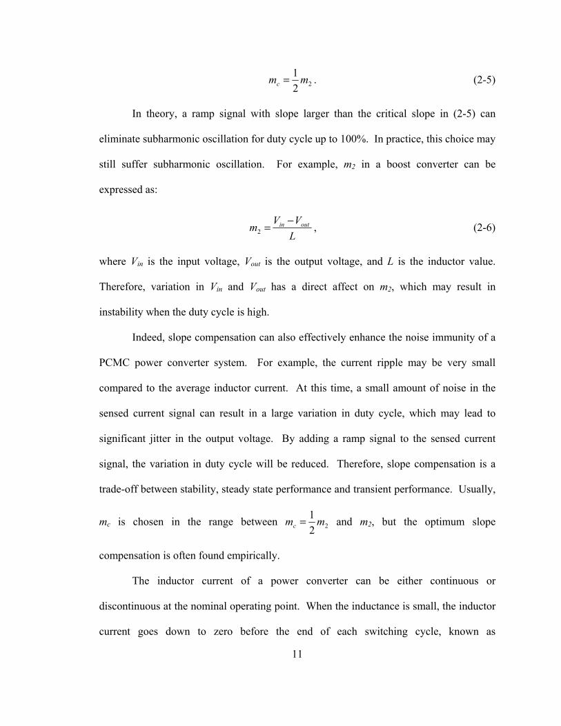
2.5 Slope compensation eliminates subharmonic oscillation (Ramp signal is ……… added to current reference) …………………………………………………… 10
2.6 Sensed switch current ………………………………………………………… 12
2.7 Block diagram of average current-mode control power converter system…… 13
2.8 Block diagram of hybrid current-mode control power converter system ……… 18
2.9 Output voltage change with duty cycle for a boost converter ………………… 20
2.10 Pin diagram of the PIC16C781/782 …………………………………………… 22
xii
2.11 Analog multiplexing diagram of the PIC16C781/782 …………………………25
2.12 A boost converter ……………………………………………………………… 37
2.13 Boost converter: (a) switch is closed, (b) switch is opened …………………… 37
3.1 Small-signal block diagram for PCMC power converter ……………………… 44
3.2 Block diagram of a PCMC boost converter controlled by a PIC16C782 ………… microcontroller ………………………………………………………………… 48
3.3 Comparison of experimental and theoretical (Ridley’s model) open-loop ……… control-to-output frequency responses of a PCMC boost converter …………… 51
3.4 Level-shift circuit ……………………………………………………………… 52
3.5 System block diagram of a PCMC power converter ………………………… 55
3.6 Bode plots of Gvc(s) for different loads ………………………………………… 56
3.7 Bode plot of zero-order-hold when sampling frequency is 25.6 µs …………… 57
3.8 Bode plots of PCMC boost converter when load is 0.187 A ………………… 58
3.9 Bode plots of HvG’vc(s) at different load ……………………………………… 61
3.10 Current loop and slope compensation circuit ………………………………… 65
3.11 Slope compensation waveforms ……………………………………………… 66
3.12 Flowchart of the main routine ………………………………………………… 68
3.13 Flowchart of the interrupt service routine (ISR) ……………………………… 69

xiii
3.14 Internal block diagram of the UC3842 ………………………………………… 70
3.15 Block diagram of a boost converter controller by a UC3842 ………………… 71
3.16 Dead time td vs. CT when RT > 5 kΩ …………………………………………… 72
3.17 A transistor is added in slope compensation circuit …………………………… 73
3.18 The PIC16C782 microcontroller controlling a PCMC boost converter ……… 75
3.19 Gate drive circuit ……………………………………………………………… 76
3.20 Transient response using the PIC16C782 when the load change was from ……… 0.75 A to 0.187 A, and KP = 1/2 and KI’ = 1/32. Output voltage: 500 …………… mV/DIV; Time: 500 μs/DIV ………………………………………………… 77
3.21 Transient response using the PIC16C782 when the load change was from ……… 0.187 A to 0.75 A, and KP = 1/2 and KI’ = 1/32. Output voltage: 500 …………… mV/DIV; Time: 500 μs/DIV …………………………………………………… 77
3.22 Step response using the PIC16C782 when the load was 0.56 A. Output ………… voltage: 5 V/DIV; Time: 500 μs/DIV ………………………………………… 78
3.23 Simulation of compensated PCMC boost converter using PI controller ………… for different load ……………………………………………………………… 79
3.24 Experimental responses of compensated PCMC boost converter using ………… digital PI controller for different load ………………………………………… 79
3.25 Transient response using the PIC16C782 when the load change was from ……… 0.75 A to 0.187 A, and KP = 1/2 and KI’ = 1/64. Output voltage: ……………… 500 mV/DIV; Time: 500 μs/DIV ……………………………………………… 80
3.26 Transient response using the PIC16C782 when the load change was from……… 0.187 A to 0.75 A, and KP = 1/2 and KI’ = 1/64. Output voltage: ……………… 500 mV/DIV; Time: 500 μs/DIV……………………………………………… 81
xiv
3.27 Transient response using analog controller when the load change was from …… 0.75 A to 0.187 A. Output voltage: 200 mV/DIV; Time: 200 μs/DIV ………82
3.28 Transient response using analog controller when the load change was from …… 0.187 A to 0.75 A. Output voltage: 200 mV/DIV; Time: 200 μs/DIV ……… 82
4.1 Typical current loop compensator …………………………………………… 84
4.2 Sun and Bass’ small signal model for an ACMC converter …………………… 86
4.3 Tang’s small-signal model for ACMC converter ……………………………… 88
4.4 Comparison of the ACMC models …………………………………………… 91
4.5 Block diagram of a hybrid ACMC converter controlled by a …………………… PIC16C782 microcontroller…………………………………………………… 92
4.6 Current loop for hybrid ACMC power converter realized on a PIC16C782 … 94
4.7 Bode plot of the current amplifier ……………………………………………… 97
4.8 Sensed current signal is biased by a dc voltage ……………………………… 98
4.9 Sensed current signal is amplified by an opamp ……………………………… 98
4.10 D/A output is scaled down by a voltage divider ……………………………… 99
4.11 The waveforms at C1 inputs …………………………………………………… 99
4.12 Bode plots of Gvc(s) for different loads ……………………………………… 102
4.13 Bode plots of ACMC boost converter when the load is 0.75 A ……………… 103
xv
4.14 Internal block diagram of UC3886 …………………………………………… 105
4.15 Schematic of the ACMC boost converter controlled by a UC3886 ………… 106
4.16 An ACMC boost converter controlled by a PIC16C782 …………………… 111
4.17 Transient response of the hybrid ACMC boost converter when the load ………… change was from 0.75 A to 0.187 A. Output voltage: 500 mV/DIV; …………… Time: 500 µs/DIV …………………………………………………………… 112
4.18 Transient response of the hybrid ACMC boost converter when the load ………… change was from 0.187 A to 0.75 A. Output voltage: 500 mV/DIV; …………… Time: 500 µs/DIV …………………………………………………………… 113
4.19 Step response of the hybrid ACMC boost converter for voltage reference ……… changing from 00h to 7Fh when load was 0.56 A. Output voltage: 5 V/DIV; …… Time: 500 µs/DIV…………………………………………………………… 115
4.20 Step response of the hybrid ACMC boost converter for voltage reference ……… changing from 7Fh to 00h when load was 0.56 A. Output voltage: 5 V/DIV; …… Time: 500 µs/DIV …………………………………………………………… 115
4.21 Transient response of the analog ACMC boost converter when the load change … was from 0.75 A to 0.18 7 A and from 0.187 A to 0.75 A. Top: The load ……… change was from 0.75 A to 0.187 A. Bottom: The load change was from ……… 0.187 A to 0.75 A. Output voltage: 1 V/DIV; Time: 1 ms/DIV …………… 116
5.1 The sets very poor students, poor student, ordinary students, good students …… and very good students are derived from students as a universe of discourse …121
5.2 The three basic fuzzy set operations ………………………………………… 123
5.3 Block diagram of fuzzy logic control algorithm ……………………………… 124
5.4 Basic membership functions: (a) triangular membership function, (b) …………… trapezoidal membership function, (c) bell-shaped membership function …… 126
xvi
5.5 Graphic representation of fuzzy reasoning …………………………………… 128
5.6 Block diagram of a fuzzy logic ACMC converter controlled by a ……………… PIC16C782 microcontroller ………………………………………………… 130
5.7 Fuzzy logic controller inside the PIC16C782 microcontroller for ACMC ……… boost converter ……………………………………………………………… 131
5.8 Membership functions for e and ce …………………………………………… 133
5.9 Membership function (1) for δvc ……………………………………………… 138
5.10 Membership function (2) for δvc ……………………………………………… 139
5.11 A fuzzy logic ACMC boost converter controlled by a PIC16C782 ………… 140
5.12 Gate and ISR timing diagram 1. Top: gate signal, 10 V/DIV; Bottom: ………… timing signal on an output pin, 2 V/DIV; Time: 5 μs/DIV…………………… 141
5.13 Gate and ISR timing diagram 2. Top: gate signal, 10 V/DIV; Bottom: ………… timing signal on an output pin, 2 V/DIV; Time: 1 μs/DIV ………………… 142
5.14 Transient response of the fuzzy logic ACMC boost converter when the load …… change was from 0.187 A to 0.75 A. Top: output voltage, 10 V/DIV; …………… Bottom: output voltage, 500 mV/DIV; Time: 500 μs/DIV ………………… 143
5.15 Transient response of the fuzzy logic ACMC boost converter when the load …… change was from 0.75 A to 0.187 A. Top: output voltage, 10 V/DIV; …………… Bottom: output voltage, 500 mV/DIV; Time: 500 μs/DIV ………………… 143
5.16 Step response of the fuzzy logic ACMC boost converter. Output voltage: ……… 5 V/DIV; Time: 500 μs/DIV ………………………………………………… 144
5.17 Block diagram of a fuzzy logic PCMC converter controlled by a PIC16C782 …… microcontroller ……………………………………………………………… 145

xvii
5.18 Membership functions for e and ce …………………………………………… 147
5.19 Membership functions for δvc ………………………………………………… 149
5.20 Fuzzy logic controller inside the PIC16C782 microcontroller for PCMC ……… boost converter ……………………………………………………………… 154
5.21 A fuzzy logic PCMC boost converter controlled by a PIC16C782 ………… 154
5.22 Gate and ISR timing diagram 1. Top: gate signal, 10 V/DIV; Bottom: ………… timing signal on an output pin, 2 V/DIV; Time: 10 μs/DIV ………………… 155
5.23 Gate and ISR timing diagram 2. Top: gate signal, 10 V/DIV; Bottom: ………… timing signal on an output pin, 2 V/DIV; Time: 1 μs/DIV ………………… 156
5.24 Transient response of the fuzzy logic PCMC boost when the load change ……… was from 0.75 A to 0.187 A. Output voltage: 500 mV/div; Time: 250 ………… μs/div………………………………………………………………………… 157
5.25 Transient response of the fuzzy logic PCMC boost when the load change ……… was from 0.187 A to 0.75 A. Output voltage: 500 mV/div; Time: 250 ………… μs/div ………………………………………………………………………… 157
5.26 Step response of the fuzzy logic PCMC boost converter for voltage …………… reference changing from 00h to 7Fh when load was 0.56 A. Output …………… voltage: 5 V/div; Time: 500 μs/div ………………………………………… 158
5.27 Step response of the fuzzy logic PCMC boost converter for voltage …………… reference changing from 7Fh to 00h when load was 0.56 A. Output …………… voltage: 5 V/div; Time: 500 μs/div ………………………………………… 158

xviii
LIST OF TABLES
3.1 Kf and Kr for different converter topologies in Ridley’s model ……………… 46
4.1 Feedforward and feedback gains for ACMC ………………………………… 89
5.1 Data base for normalization of fuzzy sets …………………………………… 125
5.2 Data base for discretization …………………………………………………… 125
5.3 Fuzzy-set values for fuzzy logic ACMC boost converter …………………… 132
5.4 Control rule table for fuzzy logic ACMC boost converter …………………… 134
5.5 Fuzzy-set values for fuzzy logic PCMC boost converter …………………… 147
5.6 Control rule table for fuzzy logic PCMC boost converter …………………… 148
5.7 Fuzzy logic lookup table (low resolution) …………………………………… 151
1
CHAPTER 1
INTRODUCTION
Current-mode control (CMC) has been a popular and effective control technique
for power converter systems for many years. Traditional CMC systems employ pure
analog components. With the development of computer technology, digital
implementation of CMC systems is becoming a practical approach.
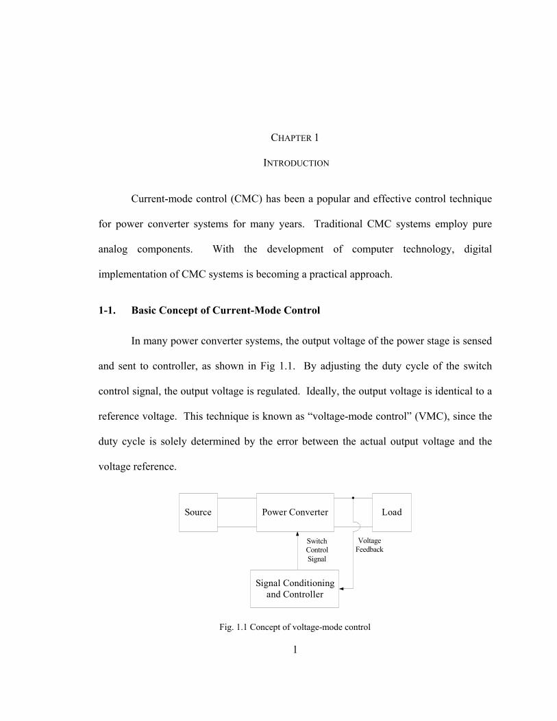
1-1. Basic Concept of Current-Mode Control
In many power converter systems, the output voltage of the power stage is sensed
and sent to controller, as shown in Fig 1.1. By adjusting the duty cycle of the switch
control signal, the output voltage is regulated. Ideally, the output voltage is identical to a
reference voltage. This technique is known as “voltage-mode control” (VMC), since the
duty cycle is solely determined by the error between the actual output voltage and the
voltage reference.
Power Converter LoadSource
Signal Conditioning and Controller
SwitchControlSignal
VoltageFeedback
Fig. 1.1 Concept of voltage-mode control

2
Another technique to regulate the power converter systems is called current-
mode control (CMC) where the inductor current is directly controlled and the output
voltage is controlled only indirectly. CMC, also called current-programmed control and
current-injected control, has existed at least since 1978 [1-2]. A CMC power converter is
typically a two-loop system (voltage loop and current loop), as shown in Fig. 1.2. The
current loop, in which the inductor current is sensed as the main controlled variable,
monitors and maintains the switch current (or inductor current) equal to a reference
current. This reference current is obtained from the voltage loop, which compares a
voltage reference to the output voltage of the power converter.
CMC has been widely used in many high-performance power supply applications
in recent years, because CMC is considered to be superior to VMC due to the fast inner
current loop. In a VMC power converter, any variation in input voltage or output load
must alter the output voltage first, and then the controller can sense the change and react
to that change by adjusting the control effort. In a CMC power converter, on the other
hand, any variation in input voltage or output load can be reflected in the inductor current
instantaneously. For this reason, CMC typically responds faster than a VMC power
converter.
Signal Conditioning and Controller
Source Power Converter Load
CurrentSignal
SwitchControlSignal
VoltageSignal
Fig. 1.2 Concept of current-mode control

3
A CMC power converter looks like a current source. Therefore, voltage variation
at the input does not go through to the output, so a CMC power converter is more
immune to an input disturbance than a VMC converter. This current source characteristic
also makes it easier to parallel current sharing among several power stages. The power
stages can be forced to share the load current equally by simply connecting the power
stages to a common control voltage. This is very valuable in high power applications.
Another advantage is that CMC converters have simpler dynamics. Their control-to-
output transfer function usually can be simplified to a first order system, and the system
can be stabilized with a simpler compensation network around the error amplifier. In
addition, CMC provides inherent over-current protection, since the inductor current is
limited on a cycle-by-cycle basis.
Comparing Fig. 1.1 and Fig. 1.2, it can be seen that a CMC system has two
control loops (voltage loop and current loop), while VMC has only one control loop
(voltage loop). Therefore, CMC is more complicated in analysis and design. CMC
system needs to sense or estimate the inductor current accurately. This may increase the
cost and/or power loss.
Despite these advantages, CMC technology has developed very fast. In the mid
90’s, Unitrode (part of Texas Instrument, Inc. today) developed a series of CMC IC chips,
which drastically advanced the application of CMC power converters. Today, CMC has
become a standard technology that has been applied widely.

4
1-2. Digital Control for Current-Mode Power Converters
Recently, digital control has been successfully applied to various switch-mode
power converter systems [91-93]. Digital control offers several important advantages
over analog control. It is easier to implement computational functions in digital control.
Some of the advanced control methods are solely suitable for digital control, such as
fuzzy logic control, adaptive control, optimal control, etc. Digital control is more flexible
in design, is easier to revise by modifying the code, and is less sensitive to noise and
environment variation. Digital control also has some important value-added features,
such as system monitoring, self-diagnostics, historical data retrieving, remote
communications or display. These features are very useful and suitable for power
management, which is attracting more and more attention with the widespread
application of portable and handheld electronic devices.
Digital control also has some disadvantages, such as sampling time delay,
computation time delay, limited computation power, control loop bandwidth, and limited
resolution due to finite word length of the processor and A/D converter. These
disadvantages may result in degradation in performance. Nevertheless, with the
increasing functionality and decreasing price, digital controllers are progressively
becoming a feasible and competitive option, especially in high-end switch-mode power
converter systems.
CMC power converters have been successfully implemented for many years using
analog circuit technology and linear system design techniques. The first current-mode
control ICs emerged about two decades ago. Currently, many semiconductor companies

5
manufacture different kinds of analog CMC IC chips. These ICs integrate together many
analog components required for CMC, and makes CMC design easy and inexpensive.
Digital control, in contrast, faces a challenge in CMC systems. Fig. 1.3 is an
inductor current waveform for a continuous conduction mode (CCM) power converter.
This waveform has a fundamental frequency equal to the switching frequency – which
can easily be in the range of hundreds of kHz. In addition, any change in input voltage or
output load reflects at the inductor current instantaneously, so the dynamics of the current
loop are fast. Therefore, pure digital implementation of the current loop requires a very
high speed analog-to-digital (A/D) converter, or a digital processor with sufficient
computational capability to estimate the inductor current.
In this dissertation, digital implementation of CMC power converter systems is
investigated, and a hybrid control method is proposed. Using this method, several
microcontroller-based CMC systems have been constructed at relatively low cost. This
dissertation also explores the implementation of fuzzy logic control on CMC power
converter systems.
nTs (n+1)Ts
Inductor Current
time
Fig. 1.3 Waveform of inductor current

6
1.3 Organization of the Dissertation
This dissertation is organized as follow:
• Chapter 2 reviews peak current-mode control and average current-mode
control, and introduces the concept of the hybrid current-mode control method.
• Chapter 3 describes the design of a microcontroller-based peak current-mode
control power converter system.
• Chapter 4 demonstrates the design of a microcontroller-based average current-
mode control power converter system.
• Chapter 5 illustrates the design of microcontroller-based fuzzy logic current-
mode control power converter systems.
• Chapter 6 presents conclusions and suggestions for future work.

7
CHAPTER 2
HYBRID CONTROL METHOD FOR CURRENT-MODE POWER CONVERTERS
Among the different ways to implement CMC, peak current-mode control (PCMC)
is probably the earliest and simplest approach, although it has some disadvantages.
Average current-mode control (ACMC) overcomes those disadvantages at the expense of
a more complicated design and analysis. In order to implement both of PCMC and
ACMC at low cost, a hybrid control method is proposed such that microcontrollers can
be used to control CMC power converters.
2-1. Peak Current-Mode Control (PCMC)
There are many ways to implement CMC, and peak current-mode control (PCMC)
is probably the earliest and simplest approach. Fig. 2.1 is the block diagram of a PCMC
power converter, and shows that a PCMC power converter is controlled with a two-loop
Source Power
Converter Load
Voltage Loop Compensator
Iref
Inductor Current
Switch ControlSignal
Comparator
VoltageFeedback
-
+
ILClock
S RQ
Fig. 2.1 Block diagram of peak current-mode control power converter system
8
?I0(k)
Vc
m 1
m2
D
I0(k)
Ip(k) Ip(k+1)
?I0(k+1) ?I0(k+2)
Ip(k+2)
I0(k+1)I0(k+2)
Fig. 2.2 For duty cycles less than 0.5, disturbances die out.
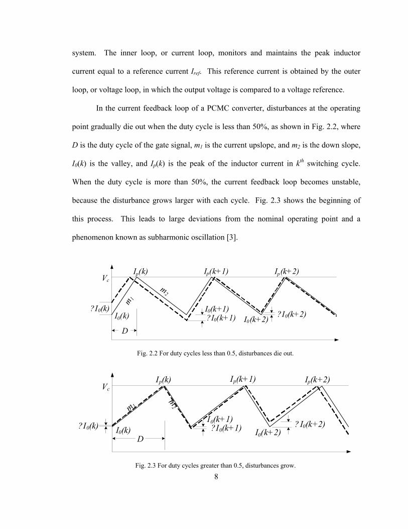
system. The inner loop, or current loop, monitors and maintains the peak inductor
current equal to a reference current Iref. This reference current is obtained by the outer
loop, or voltage loop, in which the output voltage is compared to a voltage reference.
In the current feedback loop of a PCMC converter, disturbances at the operating
point gradually die out when the duty cycle is less than 50%, as shown in Fig. 2.2, where
D is the duty cycle of the gate signal, m1 is the current upslope, and m2 is the down slope,
I0(k) is the valley, and Ip(k) is the peak of the inductor current in kth switching cycle.
When the duty cycle is more than 50%, the current feedback loop becomes unstable,
because the disturbance grows larger with each cycle. Fig. 2.3 shows the beginning of
this process. This leads to large deviations from the nominal operating point and a
phenomenon known as subharmonic oscillation [3].
Vc
m 1m
2
D
Ip(k) Ip(k+1) Ip(k+2)
?I0(k)I0(k+1) ? I0(k+2)?I0(k+1) I0(k+2)I0(k)
Fig. 2.3 For duty cycles greater than 0.5, disturbances grow.

9
Subharmonic oscillation results in an unstable system. Unfortunately,
subharmonic oscillation cannot be eliminated by simply adjusting the controller design.
This can be proved mathematically. Referring to Fig. 2.2~2.3, if the switching period is
Ts, then the duty cycle D in kth switching cycle can be expressed as:
s
0ps
0p
TmkIkI
Tm
kIkID
11
)()()()( −=
−= . (2-1)
I0(k+1) can be computed as:
s0p
0psp
sp0
TmkImmkI
mm
mkIkI
TmkI
TDmkIkI
21
2
1
2
12
2
)()(1
)()()(
)1()()1(
−−⎟⎟⎠
⎞⎜⎜⎝
⎛+=
⎟⎟⎠
⎞⎜⎜⎝
⎛ −−−=
−−=+
(2-2)
Performing z-transform to (2-2), it changes to:
1
1
21
1
2 )()(1)( −− −⎟⎟⎠
⎞⎜⎜⎝
⎛+= zzI
mmzzI
mmzI 0p0 . (2-3)
Thus,
1
2
1
21
)()(
mmz
mm
zIzI
p
0
+
+= . (2-4)
Equation (2-4) has a pole at 1
2
mm− . Since both of m1 and m2 are positive real
numbers, this pole must be at the negative real axis in z-plane, as shown in Fig. 2.4. In
order to maintain stability, this pole must be inside unit circle, i.e., m2 < m1. This
condition is satisfied only when D < 0.5.

10
In order to stabilize the system when D > 0.5, a ramp signal must be added to the
current reference or the sensed current signal, known as slope compensation [3]. As
shown in Fig. 2.5, the slope of the ramp signal, mc, will in theory cause a disturbance to
die out for any duty cycle when it is equal to or greater than half of m2. When mc = m2,
perfect rejection of disturbances on the first cycle can be achieved. However, with the
increase of mc, CMC tends to be voltage-mode control (VMC), and the advantages of
CMC will be lost. For this reason, mc should be as small as possible, as long as it can
ensure stability, and the extreme choice is:
1
1
-1
-1
m2
m1-
Real (z)
Img (z)
Fig. 2.4 Location of the pole in z-plane
Vc
m1 m2
D
mc
?I0(k+2)?I0(k)? I0(k+1)
Fig. 2.5 Slope compensation eliminates subharmonic oscillation
(Ramp signal is added to current reference)
11
221 mmc = . (2-5)
In theory, a ramp signal with slope larger than the critical slope in (2-5) can
eliminate subharmonic oscillation for duty cycle up to 100%. In practice, this choice may
still suffer subharmonic oscillation. For example, m2 in a boost converter can be
expressed as:
LVVm outin −=2 , (2-6)
where Vin is the input voltage, Vout is the output voltage, and L is the inductor value.
Therefore, variation in Vin and Vout has a direct affect on m2, which may result in
instability when the duty cycle is high.
Indeed, slope compensation can also effectively enhance the noise immunity of a
PCMC power converter system. For example, the current ripple may be very small
compared to the average inductor current. At this time, a small amount of noise in the
sensed current signal can result in a large variation in duty cycle, which may lead to
significant jitter in the output voltage. By adding a ramp signal to the sensed current
signal, the variation in duty cycle will be reduced. Therefore, slope compensation is a
trade-off between stability, steady state performance and transient performance. Usually,
mc is chosen in the range between 221 mmc = and m2, but the optimum slope
compensation is often found empirically.
The inductor current of a power converter can be either continuous or
discontinuous at the nominal operating point. When the inductance is small, the inductor
current goes down to zero before the end of each switching cycle, known as
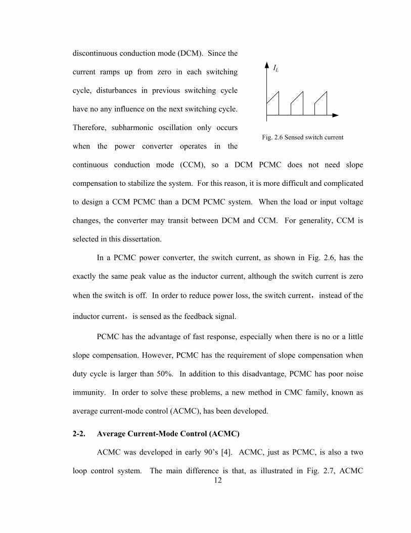
12
discontinuous conduction mode (DCM). Since the
current ramps up from zero in each switching
cycle, disturbances in previous switching cycle
have no any influence on the next switching cycle.
Therefore, subharmonic oscillation only occurs
when the power converter operates in the
continuous conduction mode (CCM), so a DCM PCMC does not need slope
compensation to stabilize the system. For this reason, it is more difficult and complicated
to design a CCM PCMC than a DCM PCMC system. When the load or input voltage
changes, the converter may transit between DCM and CCM. For generality, CCM is
selected in this dissertation.
In a PCMC power converter, the switch current, as shown in Fig. 2.6, has the
exactly the same peak value as the inductor current, although the switch current is zero
when the switch is off. In order to reduce power loss, the switch current,instead of the
inductor current,is sensed as the feedback signal.
PCMC has the advantage of fast response, especially when there is no or a little
slope compensation. However, PCMC has the requirement of slope compensation when
duty cycle is larger than 50%. In addition to this disadvantage, PCMC has poor noise
immunity. In order to solve these problems, a new method in CMC family, known as
average current-mode control (ACMC), has been developed.
2-2. Average Current-Mode Control (ACMC)
ACMC was developed in early 90’s [4]. ACMC, just as PCMC, is also a two
loop control system. The main difference is that, as illustrated in Fig. 2.7, ACMC
IL
Fig. 2.6 Sensed switch current

13
includes a compensator in the inner loop (the current loop) to average and compensate the
inductor current. The desired current level, or current reference, is set by the voltage
error amplifier in the outer loop (the voltage loop). The current error, or the difference
between averaged current and the current reference, is amplified and compared to a saw-
tooth (oscillator ramp) at the comparator inputs, where the PWM control signal is
generated.
In most cases, the average inductor current is proportional to the peak inductor
current. Therefore, ACMC can be used to replace PCMC. The current loop compensator
in an ACMC power converter acts as low-pass filter, so it can filter out switching noise
while obtaining the average inductor current.
ACMC has several important advantages over PCMC. ACMC can track the
average inductor current with a high degree of accuracy. As s result, ACMC is
particularly suitable for power factor correction (PFC), and other applications where a
constant current source is needed, since the average current is used as a controlled
Source PowerConverter Load
Voltage Loop Compensator
Inductor Current
Switch Control Signal
Comparator
VoltageFeedback
-
+
Current Loop Compensator
Sawtooth SignalClock
S RQ
Fig. 2.7 Block diagram of average current-mode control power converter system
14
quantity. ACMC eliminates the need for slope compensation, although a ramp signal is
needed. This ramp signal is independent of any signal in the power stage and the
controller, that is, this ramp signal starts from zero at each switching cycle with a preset
(fixed) slope. At the end of each switching cycle, it is driven to zero immediately.
Therefore, any current errors in previous switching cycles are washed away, and thus
excellent noise immunity is achieved.
However, the advantages of ACMC are obtained at the expense of an increased
complexity in design and analysis. Comparing with PCMC, ACMC has an extra
compensator in the current loop. The inductor current has a triangular waveform, so the
output of the current loop compensator always has some ripple. In addition, since a low-
pass filter is inserted into the current loop, its dynamics are slowed down. Therefore,
ACMC may have a slower transient response than PCMC, if slope compensation for the
PCMC power converter does not slow down the transient response.
In order to obtain a mathematical model for design purposes, a small ripple
assumption is typically employed; that is, the ripple is sufficiently small that it can be
neglected. However, this assumption may not be valid when the ripple is large – for
example, when the power converter is in DCM. As a result, the model may no be able to
predict the system behavior correctly, and thus the controller design may be inaccurate.
2-3. Efforts on Digital Implementation of Current-Mode Control
Pure digital implementation of CMC must obtain the inductor current value by
sampling through A/D conversion or estimation through other parameters. As described
previously, the frequency of the inductor current is the same as the switching frequency.
In a pure digital controller, the inductor current can be sampled in two ways: multiple
15
current samples or single current sample per switching period. With multiple current
samples per switching period, the peak, valley, slope, and average values of the inductor
current can be computed, given the duty cycle. However, this requires very high A/D
conversion speed, or multiple A/D converters, as well as high computation power.
Notice that A/D conversion frequency is different from and usually higher than the
controller sampling frequency. That is, even if high-speed A/D converter is available, the
digital processor must have enough computation power to process the sampled data in
one switching period.
Digital signal processors (DSPs) combined with high speed A/D converters can
be a solution. Ideally, A/D conversion and the reference current should be updated on a
cycle by cycle basis. This is usually impractical for a pure digital controller. However,
since the dynamics of the power stage are much slower than the switching period, the
variation of the inductor current between adjacent switching cycles should be small.
Therefore, the inductor current may be sampled or estimated at a frequency slower than
the switching frequency.
Researchers have paid a large amount of attention to the implementation of digital
CMC power converter systems. For example, in 1994, Holme and Manning developed a
digital CMC scheme [5]. This digital control system consists of three sub-systems:
analog data acquisition sub-system based on a high speed 12-bit A/D converter, 16-bit
DSP sub-system, and PWM sub-system consisting of counter circuits, latches and flip-
flops. Obviously, this early attempt had severe drawbacks because of complicated
hardware, high cost and low reliability.
16
With the development of microelectronics technology and computer technology,
the functionality of a DSP has improved significantly with drastically decreased cost.
Today, many DSPs integrate analog/digital interfaces, PWM generators, and signal
processing unit onto a single chip. In addition, because of the powerful computational
ability of a DSP, the inductor current value of a switching-mode power converter can be
estimated instead of direct measurement, and the required calculations can be completed
in one switching cycle. As a result, digital implementation of CMC is becoming a
practical approach.
For example, using sensorless CMC [6-8] and predictive CMC [9] techniques,
Kelly and Rinne proposed a solution for digital CMC using a 16-bit DSP [10]. The
inductor current is estimated from the measured load voltage of dc-dc converters and the
current estimation of previous switching cycles. Indeed, this method is an observer-based
control system where a state variable (inductor current) is observed. When using this
approach, the time delay for current estimation and calculation should not last more than
three or four switching cycles. Longer time delay results in not only more complicated
parameter estimation, but also large estimation error. Therefore, a DSP should have
sufficient computational capability to estimate the inductor current fast enough.
However, the high cost of a DSP and the associated hardware seriously restricts
its applications. Though cheaper, microcontrollers usually are not fast enough to perform
A/D conversion and computation to estimate the required parameters. Therefore, it
would be very difficult to construct a pure digital CMC system using a microcontroller.
However, a microcontroller can be integrated with some analog peripherals that can

17
compensate for the limitation in computing power while expanding the functionalities at
low cost.
2-4. Hybrid Current-Mode Control Method
As depicted previously, the fast dynamics of the current loop put forward a
difficult challenge for digital implementation of the current loop. Accordingly, analog
implementation of the current loop is much easier and more cost-effective than a digital
implementation.
In contrast, the dynamics of the voltage loop are much slower than that of the
current loop mainly because of the energy storage components (inductors and capacitors)
in the power stage. For example, the resonant frequency ω0 of the power stage (buck or
boost) can be expressed as:
LC1
0 =ω (2-7)
where L is the inductor value and C is the capacitor value. Equation (2-7) suggests that
the power stage bandwidth can be just few kilohertz. As a result, a standard digital
compensator can be used in the voltage loop straightforwardly.
Some microcontrollers have on-board analog features such as operational
amplifiers and comparators. By using these analog features, the current loop contains
only analog signals. Hence, this “analog” current loop combines with a “digital” voltage
loop to construct a hybrid controller. Fig. 2.8 is an example of a microcontroller to
control a hybrid CMC power converter.
Fig. 2.8 indicates that the microcontroller should contain some required
peripherals before it is suitable as a hybrid CMC controller. An on-board A/D converter

18
is required to convert the output voltage signal into a digital value. Since the output
voltage has relatively slow dynamics, the voltage change in adjacent switching cycles is
small. Therefore, A/D conversion for the output voltage does not have to be performed
on a cycle-by-cycle basis. Instead, the output voltage can be sampled every several
switching cycles, as long as the sampling frequency is much higher than the crossover
frequency of the power stage. Therefore, the on-board A/D converter does not have to be
very fast, since it will not be used to sample the inductor current.
In the current loop, an analog comparator is indispensable. In peak current-mode
control (PCMC), this comparator is used to generate a gate signal by comparing the peak
value of the inductor current signal to the reference current obtained by the voltage loop.
Since the output of the voltage loop is the reference current of the analog comparator in
the current loop, the comparator should have a digitally programmable reference, or a
D/A converter is required to convert the digital signal in the voltage loop to an analog
Source Power
Converter Load
A/D A/D
Microcontroller
CurrentSignal
SwitchControlSignal
D/A
VoltageLoop Controller
CurrentLoop Controller
VoltageSignal
VoltageSignal
AnalogController Digital
Controller
Fig. 2.8 Block diagram of hybrid current-mode control power converter system

19
signal. For ACMC, this comparator is used to generate the gate signal by comparing a
ramp signal to the computed control effort. Therefore, an on-board comparator is
required for both PCMC and ACMC to implement a hybrid control method.
For ACMC, an analog operational amplifier is required in the current loop to
average the current signal. Since the input of the operational amplifier is the output of
the voltage loop, a D/A converter is required to convert the digital signal in the voltage
loop to an analog signal.
It is desired to have a PWM module inside the microcontroller when the converter
operates at a constant switching frequency. An on-board PWM module can make the
procedure to generate the gate signal simpler and more reliable. Without a PWM module,
a timer must be used as an interrupt source to set the switching frequency. Many
microcontrollers do not have priority levels in their interrupt sources. In order to ensure
constant switching frequency, no other interrupt can be allowed, which may increase the
difficulty in the software design.
As described previously, a PCMC converter has subharmonic oscillation problem,
and slope compensation is required to stabilize the system. In hybrid control, the current
loop is made of analog components, so the signal in the current loop is noisy, just like a
pure analog control. Therefore, slope compensation is necessary in hybrid control. The
microcontroller should have the mechanism to generate a synchronous ramp signal to
implement slope compensation to stabilize the system when the duty cycle exceeds 50%.
In ACMC, a synchronous ramp signal is also required as the reference to generate the
gate signal. Therefore, a mechanism to generate a synchronous ramp signal is required
for both PCMC and ACMC to implement hybrid control method.

20
The output voltage Vo of a boost converter can be expressed as:
inino VD
VD
V'
11
1 =−
= , (2-8)
Equation (2-8) shows that Vo is proportional to D’. However, when D is above
80~85%, (2-8) is no longer valid, because Vo will decrease with an increased Vin when the
duty-cycle D is above approximately 85%. Fig. 2.9 shows the relationship between
output voltage and duty cycle [11], which indicates that a boost converter has two
operating point for a given Vo. Obviously, one of the operating points is not stable, so D
must be limited to less than 85% to ensure proper operating conditions. Therefore, for a
boost converter, a mechanism is needed to limit the maximum duty cycle.
The above analysis shows that the microcontroller used in hybrid CMC should
have comprehensive analog peripherals. Key peripherals include: an A/D converter, a
D/A converter, an analog comparator, a PWM module, a mechanism to generate ramp
signal, and a mechanism to limit the maximum duty cycle. For ACMC, an analog
Vin
0 0.1 0.2 0.3 0.4 0.5 0.6 0.7 0.8 0.9 1.0
Duty cycle
Fig. 2.9 Output voltage change with duty cycle for a boost converter [11]
Out
put v
olta
ge V
o

21
operational amplifier is also desired. Although it is easy to find microcontrollers that
contain some of the desired peripherals, it is not trivial to select an appropriate
microcontroller that contains all the required functionalities. For example, in [12], a
PCMC boost converter is controlled by a microcontroller, the PIC14000, which contains
an on-board analog comparator. However, the PIC14000 does not have PWM module, so
external components are required to a generate PWM signal and to limit the maximum
duty cycle. Also, this system can only operate in the discontinuous conduction mode
(DCM), since it has no slope compensation. Although slope compensation can be
implemented in this system, more external components have to be added into the system.
In [13], a single phase power factor correction system using an ACMC technique is
controlled by a hybrid controller. This controller has a microcontroller (the PIC16F887A)
to control the voltage loop. An external 512 kB EPROM is connected to the
PIC16F887A to store a lookup table. In the current loop, an analog IC chip UC3854 is
implemented to control the inductor current. In the above two examples, extra external
components are added to compensate for the deficiency of computation power of the
microcontrollers. The hybrid controllers using this approach have the disadvantages of
more complicated circuit, less reliability and higher cost than pure analog controller due
to the extra components used in the circuits. Therefore, it is important to select
appropriate microcontrollers that contain required analog peripheral features.
As long as an appropriate microcontroller can be selected, the hybrid CMC
method combines the advantages of analog control and digital control. It can handle a
high frequency current signal, while maintaining simplicity and flexibility in design.
Because the fast current loop contains only analog signals, performance will not be
22
sacrificed. Advanced digital control techniques can be implemented in the voltage loop
compensator. The current loop design is very similar to analog controllers, so design
methods and guidelines are fully established. Meanwhile, the analog current loop is not
simply an addition to the digital voltage loop. Since the analog signal and components
are inside the microcontroller, they are controlled by the microcontroller directly. For
this reason, the resulting system still can maintain the valued added features of digital
controllers, and have the full potential for power management. Compared to DSP-based
systems, this microcontroller-based system has lower cost.
2-5. The PIC16C782 Microcontroller
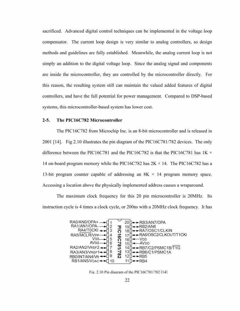
The PIC16C782 from Microchip Inc. is an 8-bit microcontroller and is released in
2001 [14]. Fig 2.10 illustrates the pin diagram of the PIC16C781/782 devices. The only
difference between the PIC16C781 and the PIC16C782 is that the PIC16C781 has 1K ×
14 on-board program memory while the PIC16C782 has 2K × 14. The PIC16C782 has a
13-bit program counter capable of addressing an 8K × 14 program memory space.
Accessing a location above the physically implemented address causes a wraparound.
The maximum clock frequency for this 20 pin microcontroller is 20MHz. Its
instruction cycle is 4 times a clock cycle, or 200ns with a 20MHz clock frequency. It has
Fig. 2.10 Pin diagram of the PIC16C781/782 [14]

23
a RISC (Reduced Instruction Set Computer) CPU core with only 35 single word
instructions. Each instruction word has 14 bits. These instructions can be completed in a
single instruction cycle, except for program branches which need two instruction cycles.
The PIC16C782 has 128 general purpose registers and 39 special function
registers. All the registers are 8-bit. The data memory is partitioned into four banks,
which contain the General Purpose Registers and the Special Function Registers. Each
bank extents up to 128 bytes with some unimplemented bytes. The lower locations of
each bank are reserved for the Special Function Registers. Some frequently used Special
Function Registers from one bank are mirrored in other banks for code reduction and
quicker access. The General Purpose Registers are at the higher locations of each bank,
and are implemented as static RAM.
The PIC16C782 has totally 16 I/O pins, 8 of them can be either analog or digital
input pins. It has up to 8 internal/external interrupt sources without priority. When an
interrupt occurs, it blocks all other interrupt sources.
The PIC16C782 has many peripheral features, and many of these features are
critical in a hybrid CMC implementation. Following is a list of important peripheral
features included in the PIC16C782:
• Two Timers
― Timer 0: 8-bit timer/counter with 8-bit prescaler
― Enhanced Timer 1: 16-bit timer/counter with prescaler
• Analog-to-Digital Converter (ADC): 8-bit resolution; programmable 8-
channel input

24
• Digital-to-Analog Converter (DAC): 8-bit resolution; reference from AVDD,
VREF1, or VR module; output configurable to VDAC pin, comparators, and
ADC reference
• Analog Operational Amplifier Module (OPA): firmware initiated input offset
voltage Auto Calibration module; programmable Gain Bandwidth Product
(GBWP)
• Dual Analog Comparator Module (C1 and C2): programmable speed and
output polarity; fully configurable inputs and outputs; reference from DAC, or
VREF1/VREF2 pins
• Voltage Reference Module (VR): 3.072V +/- 0.7% @25°C, AVDD = 5V;
configurable output to ADC reference, DAC reference, and VR pin; 5 mA
sink/source
• Programmable Switch Mode Controller Module (PSMC): PWM and PSM
modes; programmable switching frequency; slope compensation output
available; programmable minimum and maximum duty cycle.
These peripheral features of the PIC16C782 indicate that this microcontroller can
be used for a hybrid CMC system. Fig. 2.11 illustrates the connections of the analog
peripherals inside the PIC16C782 [14]. These analog components are integrated inside
the chip, and can be configured and controlled by the microcontroller through
multiplexers and control bits.
However, the PIC16C782 has limited computational ability that imposes
challenges in hardware and software design. When the PIC16C782 was selected to
implement hybrid current-mode control, there were some common issues in hardware and

25
Fig. 2.11 Analog multiplexing diagram of the PIC16C781/782 [14]
26
software design that had to be taken into account. For example, the PIC16C782 does not
have multiplication/division instructions. Instead, it has only 8-bit unsigned addition/
subtraction instructions. Therefore, the software to perform direct multiplication/division
calculations can be very complicated and very time-consuming to execute. Therefore,
direct multiplication/division is not practical for on-line control of power converters, and
must be avoided. One solution is to employ power-of-two arithmetic, where
multiplication/division can be done by simply shifting register bits left/right. However,
this arithmetic may limit the available gains, and hence may degrade the performance.
The PIC16C782 does not have a sign bit. No negative numbers can exist in the
system, and the software must keep track of the sign during calculation procedure, which
increases the size and complexity of the code considerably.
Although the PIC16C782 has the ability to address 8 kB program memory, it has
a limited internal memory space of 2 kB. External memory can increase the cost and
complexity of the circuit considerably. Therefore, the software must be concise and
should be limited to 2 kB of size.
The ADC module for the PIC16C782 captures a snapshot of the scaled output
voltage and holds it for an A/D conversion. Because of the limited sampling rate and
computation power of the PIC16C782, switching noise in the output voltage must be
avoided or filtered out in “hardware” instead of by a digital filter to ensure on-time
control. Therefore, the output voltage should be sampled during the period that has
minimum switching noise, and the sampling moment must be controlled precisely. This
can be achieved by sending back the PWM signal to an I/O pin to trigger an interrupt that
starts an A/D conversion. As a result, the sampling moment can be controlled, and the

27
output voltage can always be captured at a fixed point in the switching cycle after the
switching noise has subsided. However, the PIC16C782 does not have priority levels for
interrupts, so any other interrupt can interfere with the correct timing. In order to ensure
the proper sampling moment, an interrupt from any other source should not be allowed.
When the oscillator frequency is 20 MHz, an A/D conversion cycle requires 15.2 μs,
which equals 2.375 switching cycles. Typically, this is much faster than the total
calculation time. Therefore, the controller sampling frequency is directly determined by
the speed of the calculations instead of A/D conversion speed.
Although the PIC16C782 has limited computational ability, its adequate analog
peripheral features can largely overcome its weakness. Therefore, it has been selected to
implement various hybrid current-mode control schemes [15-20].
2-6. Digital Controller Design
When using a hybrid CMC method, the voltage loop compensator is indeed a
typical digital controller. Therefore, digital control techniques are needed to design the
voltage loop. The voltage loop compensator is a standard digital controller, and can be
designed in either the s-domain or the z-domain. When designing the digital controller in
the s-domain (emulation method), the controller Gc(s) is first designed directly in s-
domain just as an analog control system. Then Gc(s) is mapped to Gc(z) in the z-domain.
In contrast, when designing the digital controller in the z-domain, the analog plant Gp(s)
is mapped to Gp(z) first, then direct digital design techniques are utilized to design a
digital controller Gc(z) directly. In both cases, analog systems (plants or controllers) need
to be mapped into digital systems.

28
There are many existing mapping methods to perform mapping from the s-domain
to the z-domain [21-22]. These methods can be clarified into three categories: matched
pole-zero methods, input hold methods (zero-order-hold and first-order-hold) and
numerical approximations. Followings are some of the commonly used methods to
perform this transformation, given T as the sampling period:
1. Standard z-transform (matched pole-zero method).
The standard z-transform method is suitable only for band-limited signals with
maximum frequency less than half of the sampling frequency. It can be expressed as:
sTez = or zT
s ln1= . (2-9)
The standard z-transform method requires a partial-fraction expression to
complete the mapping of
1111
−−−→
+ zeas aT . (2-10)
In order to simplify the calculation, a simplified matched pole-zero method can be
used to perform the mapping:
11 −−−→+ zeas aT . (2-11)
The simplified matched pole-zero method achieves a one to one mapping of poles
and zeros. This method produces the same poles as the standard z-transform, but the
zeros are different. As a result, the simplified matched pole-zero method can be used on
non-band-limited inputs. This method is especially useful to transform an analog
controller/filter to an equivalent digital controller/filter.

29
2. Zero-order-hold (ZOH).
The transfer function of a ZOH can be expressed as:
sesG
sT
ZOH
−−= 1)( . (2-12)
Thus, Gp(z), the mapping of analog system Gp(s) using ZOH method, can be
expressed as:
⎥⎦
⎤⎢⎣
⎡−=⎥⎦
⎤⎢⎣
⎡ −=−
ssG
zz
sesGzG p
sT
pp
)(11)()( ZZ , (2-13)
where Z represents the standard z-transform. Gp(z) is known as a pulse transfer function.
The ZOH method is commonly used to transform an analog plant to its digital
representation to design its digital controller in the z-domain.
3. Numerical approximations.
By using difference equations to approximate integral and differential equations,
numerical approximation methods can be used to transform designed analog controllers
or filters to digital ones. The forward rule, backward rule and trapezoidal rule are several
of the most commonly used numerical approximation methods:
• Forward rule. The forward rule can be expressed as:
Tzs 1−= . (2-14)
The forward rule maps the left half-plane in the s- plane to the region of left side
of 1=z in the z-plane, so some stable analog designs may be unstable when they
are mapped to the z-plane.
• Backward rule. The backward rule can be expressed as:

30
zTzs )1( −= . (2-15)
The back rule maps the left half-plane in the s-plane to a circle inside the unit
circle in the z-plane. Therefore, stable analog designs always yield stable digital
designs. Indeed, even some unstable analog designs result in stable digital
designs.
• Trapezoidal (Tustin/Bilinear) rule. The trapezoidal rule can be expressed as:
)1()1(2
+−=
zz
Ts . (2-16)
This rule maps the left half-plane in the s-plane to the region inside the unit circle
in the z-plane, and the imaginary axis is mapped to the unit circle.
When the sampling frequency is high enough, all of the above methods can
deliver similar mapping results.
Traditional analog control systems are designed in the s-domain, and there are
many familiar and mature design methods. The emulation method is useful to transform
existing analog designs into digital ones. Some designers prefer the emulation method
because they are familiar with s-domain techniques. When A/D conversion speed and
controller calculation are small compared to the sampling period, one may neglect the
sampling effect and design the controller in the s-domain, and then transform the design
into the digital domain using some of the mapping methods described above, i.e.,
matched pole-zero method and numerical approximation. The emulation method ignores
A/D conversion delay and controller time delay. Therefore, the emulation method is an
approximate approach to design digital controllers,
31
Notice that the A/D conversion delay and controller time delay are different from
the actual sampling period. The A/D conversion delay is the time required for an A/D
converter to perform an A/D conversion. Controller time delay is derived from the time
required to compute the control effort. In many low-speed systems, the actual sampling
period may be much longer than A/D converter sampling and controller time delay, so
the time delay due to the A/D conversion and computation can be ignored. Sampling and
computation delay introduce additional phase shift. When the sampling period is close to
the A/D conversion delay or controller time delay, this phase shift may not be negligible
any more. At this time, the phase margin is reduced, and the system may show more
overshoot, or even be unstable. Therefore, more phase margin is desired when designing
a digital controller using the emulation method.
Indeed, it is more desirable to design digital controllers directly in the z-domain.
When using this method, the analog system transfer function Gp(s) is transformed to the
z-domain first. A ZOH is commonly used method to perform the mapping, and the
mapping can be expressed as (2-13). Note that (2-13) ignores the time delay due to A/D
conversion and computation.
However, in power converter applications, in order to achieve fast response, it is
desired to update the control effort as soon as possible, ideally on a cycle-by-cycle basis.
Since the switching frequency can easily be in the hundreds of kilohertz, so the sampling
frequency is at least several kilohertz. In this case, the A/D conversion time delay or
controller time delay usually directly determines the possible maximum sampling
frequency, and the overall time delay should be the maximum of A/D conversion delay
and controller time delay. Typically, the controller time delay is mush longer than the

32
A/D conversion time. This time delay should be considered when mapping Gp(s) to the
z-domain, and can be expressed as e-sTd in the s-plane, where Td is the controller time
delay. In this case, the sampling period equals the overall time delay, plus a short slice of
waiting time to start the next sampling for a fixed sampling frequency. When using ZOH
method, Gp(z), the mapping of Gp(s), can be expressed as:
⎥⎦
⎤⎢⎣
⎡ −= −−
dsTsT
pp esesGzG 1)()( Z . (2-17)
When the time slice is short enough to be ignored, the time delay Td
approximately equals the sampling period T. Thus, (2-17) is converted to:
⎥⎦
⎤⎢⎣
⎡−=⎥⎦
⎤⎢⎣
⎡ −= −−
ssG
zze
sesGzG psT
sT
pp
)(11)()( 2 ZZ . (2-18)
Once Gp(z) is obtained, it can be used to design the digital controller Gc(z) using
design techniques like z-domain root locus. Some existing s-domain techniques, such as
Bode plot and Routh-Hurwitz criterion, cannot be used in the z-domain directly. In order
to using those techniques, Gp(z) needs to be transformed to Gp(w):
wTwTzppp zGzGwG
)2/(1)2/(1)()()(
−+=
==W . (2-19)
Equation (2-19) indicates a bilinear transformation, which maps the region inside
the unit circle in the z-plane to the left half-plane in the w-plane. In the w-plane, those
familiar techniques can be used to design the digital controller Gc(w). After Gc(w) is
designed, it needs to be transformed back to the z-plane:

33
112)()()(
+−=
==zz
Twccc wGwGzG Z . (2-20)
MATLAB is a powerful tool to perform various transformations. In addition,
MATLAB can be used to design digital controllers directly and conveniently. For
example, the SISO Design Tool, which is opened by command sisotool( ), can be used
for this purpose [23]. Its graphical user interface allows a user to design single-
input/single-output (SISO) compensators by putting zeros and poles visually and freely in
the root locus or Bode and Nichols plots of the open-loop system, and getting the
controller directly.
In Chapter 3 and Chapter 4, a method which combines the direct digital design
method and the emulation method is proposed to design the digital controllers. In this
method, the analog plant Gp(s) is transformed to Gp(z) just as in the direct digital design
method. In this procedure, the effects of time delay and ZOH are included. Instead of
designing the controller in the z-plane or the w-plane, the controller is designed in the s-
domain. In MATLAB, command bode( ) plots the Bode diagram of a model. When the
model is a discrete-time transfer function, bode( ) maps the model into the s-plane using
z=ejωT. This procedure is equivalent to map Gp(z) back to the s-plane, with the effects of
time delay and ZOH. Based on the Bode diagram, the controller Gc(s) can be designed.
Then, using a numerical approximation, Gc(s) is converted to Gc(z). This method has the
advantage of emulation method that some existing design techniques like a Bode diagram
can be used directly without mapping to the w-plane. Meanwhile, the proposed method
considers the effects of time delay and ZOH, and thus can result in a more accurate
design.

34
When Gc(z) is obtained, it needs to be transformed to difference equations to
realize the control law. There are unlimited ways to realize the control law. Gc(z) is
essentially a digital filter, and can be represented by simulation diagram. Many digital
filter structures can be used to construct the simulation diagram [21]. The third direct
structure (3D) is one of the commonly used methods. When using this method, Gc(z) can
be written as:
∑
∑
=
−
=
−
== n
i
ii
n
i
ii
cc
zb
za
zEzVzG
0
0
)()()( . (2-21)
where Vc(z) is the controller output, and E(z) is the controller input. Therefore,
∑∑=
−
=
− −=n
ic
ii
n
i
iic zVzbzEzazV
10)()()( . (2-22)
In time domain, (2-22) can be expressed as:
∑∑==
−−−=n
ici
n
iic ikvbikeakv
10)()()( . (2-23)
Another commonly used method is to transform analog systems into discrete
state-space representations, and then use pole placement or other techniques to design the
digital controller. There are two approaches to perform the transformation to the discrete
state space model. In the first approach, the discrete state-space model is obtained from
z-domain transfer function Gp(z). At first, a simulation diagram for Gp(z) is obtained
based on the selected digital filter structure. Then, the state-space model can be derived
from the simulation diagram. Some typical state space representations can be directly

35
written out based on Gp(z) without the assistance of a simulation diagram. For example,
if Gp(z) can be expressed as:
011
1
011
1
......)(
azazazbzbzbzG n
nn
nn
p +++++++= −
−
−− , (2-24)
then its controllable canonical form can be expressed as:
[ ]
⎥⎥⎥⎥⎥⎥
⎦
⎤
⎢⎢⎢⎢⎢⎢
⎣
⎡
−−−−=
⎥⎥⎥⎥⎥⎥
⎦
⎤
⎢⎢⎢⎢⎢⎢
⎣
⎡
+
⎥⎥⎥⎥⎥⎥
⎦
⎤
⎢⎢⎢⎢⎢⎢
⎣
⎡
⎥⎥⎥⎥⎥⎥
⎦
⎤
⎢⎢⎢⎢⎢⎢
⎣
⎡
−−−−
=
⎥⎥⎥⎥⎥⎥
⎦
⎤
⎢⎢⎢⎢⎢⎢
⎣
⎡
++
++
−
−−
−
−−
−
)()(
)()(
)(
)(
10
00
)()(
)()(
1000
00000010
)1()1(
)1()1(
1
2
1
1210
1
2
1
1210
1
2
1
kxkx
kxkx
bbbbky
ku
kxkx
kxkx
aaaakxkx
kxkx
n
n
nn
n
n
nnn
n
ML
MM
L
L
MOM
L
L
M
. (2-25)
Another approach to obtain a discrete state-space model is to compute it from the
continuous state-space model. If the continuous state space model is expressed as:
)()()()()(
tCXtYtBUtAXtX
=+=
, (2-26)
then the discrete model can be expressed as:
[ ]
CC
BdTB
AsITA
kXCkYkUBkXAkX
d
T
d
Ttd
d
dd
=⎥⎦⎤
⎢⎣⎡ −Φ=
−=Φ=
=+=+
∫=
−−
0
11
)(
)()(
:where)()(
)()()1(
ττ
L (2-27)

36
The transformation also can be easily realized using MATLAB. As long as a
discrete state-space model is obtained, the digital controller can be designed directly
based on the model. Pole placement is one of the commonly used methods to design the
controllers. Desired poles are mapped from the s-plane to the z-plane using z=esT, and
then the feedback gain matrix K is selected to ensure that the eigenvalues of [Ad – BdK]
equal the desired poles. Observers are usually needed to estimate the states.
The state-space control method, also know as the modern control method, has
become a very powerful approach to analyze and design control systems. However,
state-space control method usually requires a more accurate system model. In addition,
this method usually involves many floating point calculations and its feedback gains need
to be accurate. Therefore, the state-space control method may be difficult to apply to ill-
defined systems. For nonlinear power converter systems, their transfer functions are
approximations. Even worse, their transfer functions may change with operating
conditions. Microcontrollers usually have limited resolution and computation capacity.
Therefore, when using microcontrollers to control power converter systems, state space
control method may not be able to compute an accurate control effort fast enough to
ensure proper operation of the power stage. Therefore, the state-space control method is
not used in this dissertation. Though, it is still useful to analyze the systems off-line.
2-7. Boost Converter
Boost converter is one of the basic dc-dc converter topologies. It can produce an
output voltage higher than the input voltage. However, the boost converter has a right-
half plane zero in its control-to-output transfer function. Thus, it has a more complicated
dynamics than other simple topologies. In addition, as discussed previously, the

37
maximum duty cycle of a boost converter must be limited to ensure stability. For
generalization, boost converter is selected in this research.
Fig. 2.12 illustrates a boost converter. Obviously, a boost converter is a time-
varying nonlinear system because of the switching behavior in the circuit. In order to
obtain the transfer function of the boost converter for design purposes, the system must
be linearized first. Usually, the averaged switch model [3] is used to derive the transfer
function. In order to simplify the derive process, ESRs of the inductor and the output
capacitor are ignored.
A boost converter can be viewed as Fig. 2.13, in which Fig. 2.12 is split into two
states: the switch is closed and the switch is opened. In each state, the system is linear.
Fig. 2.13 (a) can be expressed as:
Rv
dtdvC oo −= , and in
L vdtdiL = . (2-28)
RC
L
Vin
iL
+
vo
-
RCVin
+
vo
-
LiL
(a) (b)
Fig. 2.13 Boost converter: (a) switch is closed, (b) switch is opened
RC
L
VinPWM signal
+
Vo
-
Fig. 2.12 A boost converter

38
That is:
inL
o
L
o vL
iv
RCiv
dtd
⎥⎥
⎦
⎤
⎢⎢
⎣
⎡+⎥
⎦
⎤⎢⎣
⎡⎥⎥
⎦
⎤
⎢⎢
⎣
⎡−=⎥
⎦
⎤⎢⎣
⎡10
00
01. (2-29)
Fig. 2.13 (b) can be written as:
Rvi
dtdvC o
Lo −= , and oin
L vvdtdiL −= . (2-30)
That is:
inL
o
L
o vL
iv
L
CRCiv
dtd
⎥⎥
⎦
⎤
⎢⎢
⎣
⎡+⎥
⎦
⎤⎢⎣
⎡
⎥⎥⎥⎥
⎦
⎤
⎢⎢⎢⎢
⎣
⎡
−
−=⎥
⎦
⎤⎢⎣
⎡10
01
11
. (2-31)
Using the averaged switch model, when the duty cycle is D, the average of (2-29)
and (2-31) can be expressed by:
⎟⎟⎟⎟
⎠
⎞
⎜⎜⎜⎜
⎝
⎛
⎥⎥
⎦
⎤
⎢⎢
⎣
⎡+⎥
⎦
⎤⎢⎣
⎡
⎥⎥⎥⎥
⎦
⎤
⎢⎢⎢⎢
⎣
⎡
−
−+
⎟⎟⎟
⎠
⎞
⎜⎜⎜
⎝
⎛
⎥⎥
⎦
⎤
⎢⎢
⎣
⎡+⎥
⎦
⎤⎢⎣
⎡⎥⎥
⎦
⎤
⎢⎢
⎣
⎡−=⎥
⎦
⎤⎢⎣
⎡in
L
oin
L
o
L
o vL
iv
L
CRCdvL
iv
RCdiv
dtd
10
01
11
'10
00
01
inL
o
L
o vL
iv
Ld
Cd
RCiv
dtd
⎥⎥
⎦
⎤
⎢⎢
⎣
⎡+⎥
⎦
⎤⎢⎣
⎡
⎥⎥⎥⎥
⎦
⎤
⎢⎢⎢⎢
⎣
⎡
−
−=⎥
⎦
⎤⎢⎣
⎡⇒ 1
0
0'
'1
. (2-32)
For large signals, vin = Vin, vo = Vo, iL = IL, d = D and d’ = D’ all are constant, so:
010
0'
'1
=⎥⎥
⎦
⎤
⎢⎢
⎣
⎡+⎥
⎦
⎤⎢⎣
⎡
⎥⎥⎥⎥
⎦
⎤
⎢⎢⎢⎢
⎣
⎡
−
−in
L
o VL
IV
LD
CD
RC , (2-33)

39
That is:
⎪⎪⎩
⎪⎪⎨
⎧
=
=
'
'1
RDVI
DVV
oL
in
o
. (2-34)
Equation (2-34) is the familiar large-signal dc model for the boost converter.
Average small-signal ac model for a boost converter can also be obtained through (2-32).
In order to obtain the control effort to output transfer function, )(ˆ)(ˆ
)(sdsvsG o
vd = , it is
assumed vin = Vin = constant. When there is a positive duty cycle perturbation
dD ˆ+ (which is equivalent to dD ˆ'− ), both vo and iL will increase a little bit. Thus, (2-32)
can be written as:
inLL
o
L
o VL
iI
vV
LdD
CdD
RCi
vdtd
⎥⎥
⎦
⎤
⎢⎢
⎣
⎡+⎥
⎦
⎤⎢⎣
⎡
+
+
⎥⎥⎥⎥
⎦
⎤
⎢⎢⎢⎢
⎣
⎡
−−
−−=⎥
⎦
⎤⎢⎣
⎡10
ˆˆ
0ˆ'
ˆ'1
ˆˆ 0 . (2-35)
Rearrange (2-35), following equation can be obtained:
.ˆˆ
0ˆ
ˆ00
0'
'1
0ˆ
ˆ0
ˆˆ
0'
'1
ˆˆ
⎥⎦
⎤⎢⎣
⎡
⎥⎥⎥⎥
⎦
⎤
⎢⎢⎢⎢
⎣
⎡ −
+⎥⎥
⎦
⎤
⎢⎢
⎣
⎡+⎥
⎦
⎤⎢⎣
⎡
⎥⎥⎥⎥
⎦
⎤
⎢⎢⎢⎢
⎣
⎡
−
−+
⎥⎦
⎤⎢⎣
⎡
⎥⎥⎥⎥
⎦
⎤
⎢⎢⎢⎢
⎣
⎡ −
+⎥⎦
⎤⎢⎣
⎡
⎥⎥⎥⎥
⎦
⎤
⎢⎢⎢⎢
⎣
⎡
−
−=⎥
⎦
⎤⎢⎣
⎡
L
o
inL
o
L
o
L
o
L
o
i
v
Ld
Cd
LVI
V
LD
CD
RC
IV
Ld
Cd
i
v
LD
CD
RCi
vdtd
(2-36)

40
Substitute (2-34) into (2-36), ⎥⎥
⎦
⎤
⎢⎢
⎣
⎡+⎥
⎦
⎤⎢⎣
⎡
⎥⎥⎥⎥
⎦
⎤
⎢⎢⎢⎢
⎣
⎡
−
−
LVI
V
LD
CD
RCin
L
o0
0'
'1
is canceled out. Also,
considering that 'd , Li and ov are small signal perturbations, their product should be very
small. Therefore, the term ⎥⎦
⎤⎢⎣
⎡
⎥⎥⎥⎥
⎦
⎤
⎢⎢⎢⎢
⎣
⎡ −
L
o
i
v
Ld
Cd
ˆˆ
0ˆ
ˆ0
=
⎥⎥⎥⎥
⎦
⎤
⎢⎢⎢⎢
⎣
⎡−
LvdC
id
o
L
ˆˆ
ˆˆ
is approximately zero. Thus, (2-36)
can be rewritten as:
.0
ˆ
ˆ0
ˆˆ
0'
'1
ˆˆ
⎥⎦
⎤⎢⎣
⎡
⎥⎥⎥⎥
⎦
⎤
⎢⎢⎢⎢
⎣
⎡ −
+⎥⎦
⎤⎢⎣
⎡
⎥⎥⎥⎥
⎦
⎤
⎢⎢⎢⎢
⎣
⎡
−
−=⎥
⎦
⎤⎢⎣
⎡
L
o
L
o
L
o
IV
Ld
Cd
i
v
LD
CD
RCi
vdtd (2-37)
Rearrange (2-37) and replace IL by (2-34), then (2-37) becomes:
.ˆ'ˆˆ
0'
'1
ˆˆ
d
LVRCD
V
i
v
LD
CD
RCi
vdtd
o
o
L
o
L
o
⎥⎥⎥⎥
⎦
⎤
⎢⎢⎢⎢
⎣
⎡−+⎥
⎦
⎤⎢⎣
⎡
⎥⎥⎥⎥
⎦
⎤
⎢⎢⎢⎢
⎣
⎡
−
−=⎥
⎦
⎤⎢⎣
⎡ (2-38)
The control-to-output transfer function Gvd(s) can be derived as:
⎥⎥⎥⎥
⎦
⎤
⎢⎢⎢⎢
⎣
⎡−
⎥⎥⎥⎥
⎦
⎤
⎢⎢⎢⎢
⎣
⎡ −+==
−
LVRCD
V
sLD
CD
RCs
sdsvsG
o
o
ovd
''
'1
]01[)(ˆ)(ˆ
)(
1
2
22
2
''1
'1
')(
sDLCs
RDL
sRD
L
DVsG o
vd
++
−= . (2-39)

41
Similarly, the control-to-inductor-current transfer function Gid(s) can be derived
as:
⎥⎥⎥⎥
⎦
⎤
⎢⎢⎢⎢
⎣
⎡−
⎥⎥⎥⎥
⎦
⎤
⎢⎢⎢⎢
⎣
⎡ −+==
−
LVRCD
V
sLD
CD
RCs
sdsisG
o
o
Lid
''
'1
]10[)(ˆ)(ˆ
)(
1
2
22
2
''1
)2
1('
2
)(s
DLCs
RDL
sRCRD
V
sGo
id
++
+= . (2-40)
Equation (2-38) is the linearized state space representation of the open-loop boost
converter, and (2-39) and (2-40) are its corresponding transfer functions. Notice that (2-
33) ~ (2-40) are based on the assumption that variations of the inductor current iL are very
small. This assumption is valid only when the boost converter operates at CCM.
Therefore, (2-38) ~ (2-40) only represent the CCM boost converter model. For DCM, the
model described here is no longer valid. Since CCM is selected in this dissertation, the
DCM boost converter model is not derived here.
The CCM boost converter model is derived with another assumption that Vin and
R are constant. When Vin or R changes, the system model also changes. Therefore, the
compensator designed at nominal conditions may not operate correctly when Vin or R
changes to other values. Indeed, it is commonly desired that the system can operate
correctly under other possible conditions. Therefore, possible operating conditions
should be determined first before designing the controller, which should have enough
stability margins to compensate for the uncertainty.

42
Equation (2-39) shows that the boost converter has a right half-plane zero. This
zero in Gvd(s) has negligible magnitude at low frequency. However, at high frequency, it
causes a phase reversal. Therefore, it is difficult to obtain a traditional single-loop
controller with wide bandwidth.
43
CHAPTER 3
MICROCONTROLLER-BASED PEAK CURRENT-MODE CONTROL
In order to demonstrate the feasibility of a microcontroller-based hybrid CMC
power converter, a peak current-mode controlled (PCMC) boost converter operating in
the continuous conduction mode (CCM) has been designed and implemented using a
PIC16C782 microcontroller. This microcontroller-based hybrid PCMC controller has
been compared to a pure analog controller based on a UC3842, an analog chip
manufactured by Texas Instruments, Inc.
3-1. Modeling Peak Current-Mode Control
When designing a PCMC power converter, an ac equivalent circuit model of the
PCMC converter is needed, especially control-to-output transfer function.
A large number of continuous-time models for PCMC converters have been
presented since PCMC was first proposed in 1978 [1-2]. There are two generally
accepted models for PCMC converters: one was proposed by Ridley in 1991 [23-25], and
another by Tan in 1994 [26-28]. Both models include a high-frequency extension so that
thay are accurate up to half the switching frequency. In addition, both models can be
applied to different types of power converter topologies.
The block diagram of Ridley’s model is shown in Fig. 3.1. The terms in the
diagram are defined as following:
• inv , the perturbation of the input voltage of the power stage.

44
• ov , the perturbation of the output voltage.
• Li , the perturbation of the inductor current.
• d , the perturbation of the duty cycle that controls the switch in the power
stage.
• Gvd(s), the control-to-output transfer function of the power converter, which
can be expressed as
dvsG o
vd ˆˆ
)( = (3-1)
• Gid(s), inductor current transfer function of the power converter, which can be
expressed as:
disG L
id ˆˆ
)( = (3-2)
• He(s) is the sampling gain, which is used to model the sampling action in the
current loop.
Power Stage Gvd(s), Gid(s)
Kf
He(s)
Rid
–
++
+Kr
vin^
vc^
vo^
Fm
iL
Fig. 3.1 Small-signal block diagram for PCMC power converter [23-25]

45
• Ri, the effective linear gain (volts/amp) from the sensed current to the
comparator input.
• Fm, the modulator gain which is the ac gain from the error current signal to the
duty cycle.
• Kf and Kr are the feedforward and feedback gains.
The following terms are used in the model:
• Se, the slope of the external compensation ramp (volts/sec) at the comparator
input.
• Sn, the slope of the sensed current ramp (volts/sec) at the comparator input.
• Ts, the switching period.
The sampling gain He(s) and modulator gain Fm can be computed by:
2
2
1)(nzn
es
QssH
ωω++≅ (3-3)
sn T
πω = (3-4)
π2−=zQ (3-5)
snem TSS
F)(
1+
= (3-6)
Fm is usually a constant and can only be affected by the external ramp signal, Se.
Feedforward and feedback gain terms Kf and Kr are different for different types of
converters. Table 3.1 lists Kf and Kr for three basic types of converters.

46
Tan’s model [26-28] uses different notation, which is equivalent to Ridley’s
model by the following conversions:
,,,ˆˆ21 ifinicc RSMRSMRvi === and iee RSM = (3-7)
The system block of Tan’s model is similar to Ridley’s model, but the contents
inside the block are different. In Tan’s model,
kKkK rf βα == , (3-8)
where α = 1, 0, 1, and β = 0, 1, 1, respectively for the buck, boost, and buck-boost
converter, and:
LDDk
2′
= (3-9)
Tan’s unified modulator gain can be expressed as:
sioff
ne
m
TLRV
SSF
)2
(
1
−+= (3-10)
where Voff is the dc voltage applied between the active and passive terminals of the switch
element. Indeed, Voff appears across either switch (main switch or diode) when it is off.
This equation suggests that the only difference between Tan’s and Ridley’s modulator
Table 3.1 Kf and Kr for different converter topologies in Ridley’s model [24-25]
Buck Boost Buck-Boost
Kf ⎟⎠⎞
⎜⎝⎛ −−
21 D
LTDR si
LTR si
2− ⎟
⎠⎞
⎜⎝⎛ −−
21 D
LTDR si
Kr LTR si
2−
LTRD si
2
2′
LTRD si
2
2′

47
gain equations is the term LRV ioff
2− . If there is no slope compensation ramp (Se), the term
LRV ioff
2− allows Tan’s modulator gain Fm to go infinity when
LRV
S ioffn 2
= , then changes
sign as the duty cycle goes above 50%. This is sure to cause instability, which intuitively
agrees with the subharmonic oscillation at 50% duty cycle and above without slope
compensation.
Tan’s model does not include the sampling gain He(s), i.e., He(s) = 1. Instead,
Tan’s model includes the sampling effect by adding an extra pole, ωp, to the modulator
gain, Fm. Therefore, modified Fm can be expressed as:
⎟⎟⎠
⎞⎜⎜⎝
⎛+−+
=
ps
ioffne
msT
LRV
SSF
ω1)
2(
1 (3-11)
)5.0'( −==
DmQ c
nnp π
ωωω (3-12)
n
eec S
SMMm +=+= 11
1
(3-13)
Many later papers extend these two models or derive new models [29-35] such
that a more accurate model can be achieved. However, these two models are accurate
enough for design purpose in most cases. Considering the tradeoff between the accuracy
and model complexity, Ridley’s model often has been chosen for design.
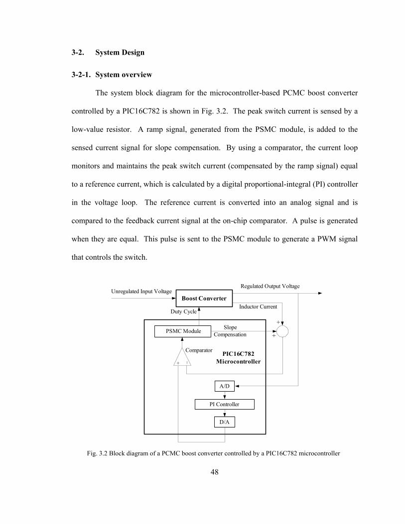
48
3-2. System Design
3-2-1. System overview
The system block diagram for the microcontroller-based PCMC boost converter
controlled by a PIC16C782 is shown in Fig. 3.2. The peak switch current is sensed by a
low-value resistor. A ramp signal, generated from the PSMC module, is added to the
sensed current signal for slope compensation. By using a comparator, the current loop
monitors and maintains the peak switch current (compensated by the ramp signal) equal
to a reference current, which is calculated by a digital proportional-integral (PI) controller
in the voltage loop. The reference current is converted into an analog signal and is
compared to the feedback current signal at the on-chip comparator. A pulse is generated
when they are equal. This pulse is sent to the PSMC module to generate a PWM signal
that controls the switch.
Boost Converter
PI Controller
Comparator
PSMC Module
Unregulated Input VoltageRegulated Output Voltage
Inductor CurrentDuty Cycle
PIC16C782Microcontroller+ _
Slope Compensation
+
+
A/D
D/A
Fig. 3.2 Block diagram of a PCMC boost converter controlled by a PIC16C782 microcontroller

49
Fig. 3.2 reflects the hybrid control method in the design. By using the on-board
comparator and PSMC module, the analog current loop and digital voltage loop are
integrated onto a single microcontroller.
For the laboratory prototype, the nominal input and output voltages of the boost
converter are 12 V and 28 V, respectively, and the nominal load is 50 Ω (0.56 A). The
switching frequency is 156.25 kHz, and the system operates in CCM.
3-2-2. Current-loop design
When designing the control system, the current loop should be designed first.
Since there is no compensator in the current loop of a PCMC converter system, current
loop design is relatively simple. Two issues are involved in designing the current-loop:
the method and gain of the current sensing and the slope of the ramp signal for slope
compensation.
The inductor current can be sensed directly using a low-value resistor or a
transformer. A sense resistor is a simple and inexpensive approach. In order to ensure
that the value of the sensed signal is in a usable range and the sensed signal is within the
normal operational range of the comparator circuit, the sense resistor should provide
sufficient gain, which may result in significant power loss, especially at high current
situations. Sometimes, it may be necessary toutilize an amplifier as a low-pass filter to
amplify the current signal while filtering out high frequency switching noise.
A transformer can be used to sense the current. Typically, this transformer has a
1-turn primary and a n-turn secondary winding. A transformer can reduce power loss in
the circuit and provide excellent isolation between the power stage and the control circuit.
The main disadvantage of the transformer approach is the higher cost and increased
50
design complexity.
In this implementation, the switch current, whose peak value is the same as the
inductor current, is sensed by a low-value resistor. Since the sensed current signal can be
very noisy, a simple RC low-pass filter is added to filter out noise.
The external ramp signal for slope compensation is generated by the PSMC
module and an RC network. Slope compensation design will be discussed in detail later
in Section 3-2-5, which depicts the design considerations regarding the PSMC module.
When the current loop is closed, the control-to-output transfer function, Gvc(s), is
useful in designing the voltage loop. Using Ridley’s model, Gvc(s) can be derived from
Fig. 3.1 as:
)()()(1)(
ˆˆ
)(sGKFsGsHRF
sGFvvsG
vdrmideim
vdm
c
ovc −+
== , (3-14)
where DDLVS
LRTDK i
nis
r −=== 1',,2
'2. Gvd(s) and Gid(s) for a boost converter have
been derived in Chapter 2, referring to (2-39) and (2-40). The actual transfer function
Gvc(s) has an infinite number of poles. In a practical design, since high frequency zeros
or poles can be neglected, Gvc(s) can be simplified to a second order system or generated
from experimental measurements after the slope the ramp signal Se is selected. Since
Gvc(s) is an approximation of actual transfer function, error always exists. A more
accurate and simple method is to measure the transfer function directly. In this
implementation, a network analyzer (Model 102B form AP Instrument Inc.) is used to
measure the frequency response of the PCMC system with the current loop closed. The
transfer function can be obtained by using MATLAB to fit it to the measured frequency

51
response data. Fig. 3.3 shows the measured open-loop control-to-output frequency
response of a PCMC boost converter and its theoretical frequency response using
Ridley’s model. It can be seen from Fig. 3.3 that the theoretical calculation is close to the
experimental measurement up to half of the switching frequency. Obviously, it is more
desirable to use measured model for design purpose when it is available.
3-2-3. Analog to digital conversion (ADC) and time delay
In the proposed hybrid control scheme, the voltage loop is implemented digitally.
Therefore, the output voltage vo of the power stage must be sampled as the feedback to
the voltage loop compensator. The ADC module inside the PIC16C782 captures a
snapshot of the sampled signal and holds it for an A/D conversion. It is required that
the A/D conversion should have adequate resolution to ensure proper measurement of
102 103 104
-20
0
20
40
60
Mag
nitu
de (d
b)
Experimental ResponseTheoretical Response (Ridley's Model)
102 103 104
-300
-200
-100
0
Frequency (rad/sec)
Pha
se (d
eg)
Fig. 3.3 Comparison of experimental and theoretical (Ridley’s model) open-loop control-to-output frequency responses of a PCMC boost converter

52
the output voltage. This resolution is determined by the range of measurement and the
word length of the digital value. In this implementation, the nominal output voltage of
the boost converter is 28 V, so the output voltage can easily be higher than 30 V. Since
the ADC module has an 8-bit resolution, the A/D conversion error can be easily more
than 0.12 V when the possible full range of output voltage (0-30 V or more) is measured.
In order to get higher A/D resolution, a level-shift circuit has been designed such
that the A/D result represents a “windowed” range of the output voltage around the
nominal value. The level shifter is built from an external operational amplifier with
several resistors. An external voltage buffer (voltage follower) is needed to ensure
accurate measurement of the output voltage. In this implementation, shown in Fig. 3.4,
the dc bias voltage is set to 2.5 V, and the gain of the opamp is set to 12. This design can
measure the “windowed” range of 25.67 V and 30.33 V for a 28 V nominal output
voltage. The level shifter can be built from the internal OPA module with several
external resistors. An external voltage buffer (voltage follower) is needed to ensure
accurate measurement of the output voltage. Another channel is used to measure the full-
range output voltage with lower resolution. This channel is not used during normal
+ _
+ _
5 V
ADC
ADC
Power Stage Output
~
Voltage Follower
10 kO
1 kO20 kO
240 kO
10 kO 10 kO
1 nF
1 kO
Fig. 3.4 Level-shift circuit

53
operation in this implementation, because the variation in the output voltage resulting
from a possible disturbance is within this window range. However, this channel can be
used to implement a soft-start when the startup ramp of the output voltage needs to be
precisely controlled. When the ADC resolution is satisfactory for an application, the
level-shift circuit can be eliminated, and hence the external voltage buffer can be
eliminated also.
Since the current-loop is constructed using analog components, the signal in the
current loop instantaneously varies with the inductor current without time delay.
Therefore, it is desirable to update the current reference, which is the output of the
voltage loop, at the beginning of each switching cycle.
However, this ideal situation is difficult to achieve when using a PIC16C782 to
control a power converter. Because of the limited computation power of PIC16C782 and
the fast dynamics of the power stage, the delays due to A/D conversion and control
computation cannot be neglected. For example, in this implementation, the switching
frequency is 156.25 kHz for a switching period of 6.4 μs. When the oscillator frequency
is 20 MHz, an A/D conversion cycle requires 15.2 μs, which equals 2.375 switching
cycles. For a 20 MHz oscillator frequency, the instruction cycle (the time to execute an
instruction) is 0.2 μs, so only 32 instructions can be executed in each switching cycle.
This implies that even a very simple control law is difficult to be completed in a single
switching cycle. In this implementation, nearly 4 switching cycles (or nearly 25.6 μs) are
needed to finish the calculation of the control law. A/D conversion and calculations can
be performed simultaneously, but the A/D conversion time is much faster than the
calculation time (controller time delay), so the calculation time directly determines the

54
sampling period. In order to achieve constant sampling frequency, there is a short
waiting period (less than a switching cycle, or 6.4 μs, in this implementation) before
starting the next sampling period. When this waiting period is neglected, the controller
sampling period approximately equals the controller time delay, or 25.6 μs. In order to
update the current reference as soon as possible, the controller time delay should be as
short as possible. Therefore, compact software design is critical in this implementation.
Switching noise in the output voltage is inevitable. In order to achieve concise
software, switching noise in the output voltage should be avoided or filtered out in
“hardware” instead of by a digital filter. Digital filter is indeed not practical in this
implementation, because the switching noise contains harmonics with frequency much
higher than possible sampling frequency. Therefore, the output voltage should be
sampled during the period that has minimum switching noise. In this implementation, the
PWM signal is sent back to another I/O pin to trigger an interrupt that starts an A/D
conversion, so the sampling moment can be controlled accurately, and the output voltage
can always be captured after the switching noise has subsided. Since the PIC16C782
does not have priority levels for interrupts, an interrupt from any other source should not
be allowed to ensure constant sampling rate and the proper sampling moment. The
starting point of each A/D conversion cycle can be controlled precisely at a 0.2 μs (one
instruction cycle) precision.
3-2-4. Voltage-loop controller design
Once the current loop is designed, the converter with the closed current loop can
be treated as a “new” open-loop plant, and the voltage loop compensator Gc(s) is
designed to control the “new” plant Gvc(s). The “new” system, shown in Fig. 3.5, is
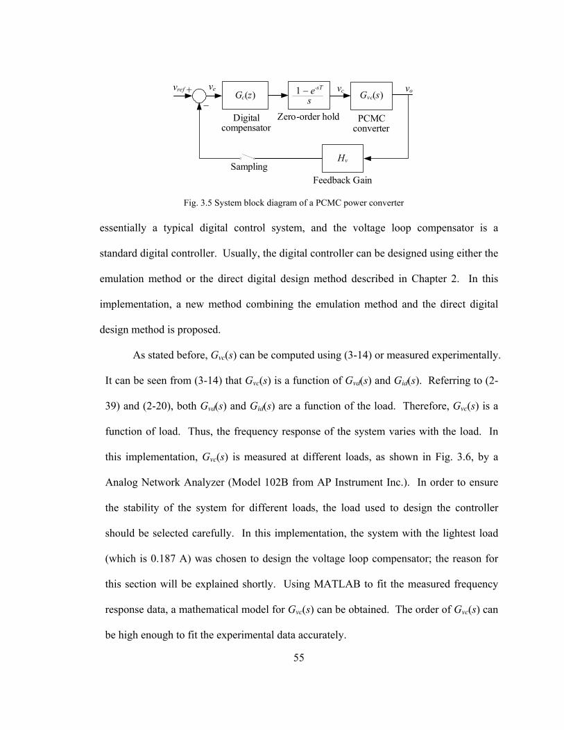
55
essentially a typical digital control system, and the voltage loop compensator is a
standard digital controller. Usually, the digital controller can be designed using either the
emulation method or the direct digital design method described in Chapter 2. In this
implementation, a new method combining the emulation method and the direct digital
design method is proposed.
As stated before, Gvc(s) can be computed using (3-14) or measured experimentally.
It can be seen from (3-14) that Gvc(s) is a function of Gvd(s) and Gid(s). Referring to (2-
39) and (2-20), both Gvd(s) and Gid(s) are a function of the load. Therefore, Gvc(s) is a
function of load. Thus, the frequency response of the system varies with the load. In
this implementation, Gvc(s) is measured at different loads, as shown in Fig. 3.6, by a
Analog Network Analyzer (Model 102B from AP Instrument Inc.). In order to ensure
the stability of the system for different loads, the load used to design the controller
should be selected carefully. In this implementation, the system with the lightest load
(which is 0.187 A) was chosen to design the voltage loop compensator; the reason for
this section will be explained shortly. Using MATLAB to fit the measured frequency
response data, a mathematical model for Gvc(s) can be obtained. The order of Gvc(s) can
be high enough to fit the experimental data accurately.
Hv
Gc(z) Gvc(s)_
Digital compensator
+vref ve vc vo1 – e-sT
sZero-order hold
SamplingFeedback Gain
PCMCconverter
Fig. 3.5 System block diagram of a PCMC power converter

56
Once Gvc(s) is obtained, it can be converted to a discrete-time model Gvc(z) using
the zero-order hold (ZOH) method. The ZOH, as expressed in (2-12), introduces a phase
lag and magnitude reduction to the system. This can be seen clearly in its Bode plot
shown in Fig. 3.7. In this implementation, the total time delay is approximately four
times the switching period (6.4 μs), so 25.6 μs is used as the controller sampling period.
According to (2-13), Gvc(z) can written as:
⎥⎦⎤
⎢⎣⎡−=
ssG
zzzG vc
vc)(1)( Z . (3-15)
As stated previously, the calculation time is approximately equal to the sampling
period. Considering the time delay, the mapping of Gvc(s), referring to (2-18), can be
-20
-10
0
10
20
30
40
Mag
nitu
de (d
B)
102
103
104
105
-180
-135
-90
-45
0
Phas
e (d
eg)
Bode Diagram
Frequency (rad/sec)
0.187 A0.56 A0.75 A
Fig. 3.6 Bode plots of Gvc(s) for different loads
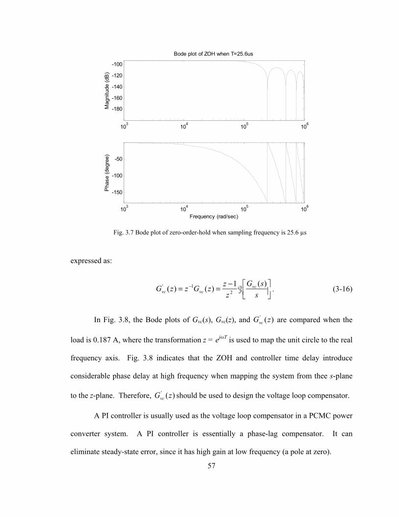
57
expressed as:
⎥⎦⎤
⎢⎣⎡−== −
ssG
zzzGzzG vc
vcvc)(1)()( 2
1' Z . (3-16)
In Fig. 3.8, the Bode plots of Gvc(s), Gvc(z), and )(' zGvc are compared when the
load is 0.187 A, where the transformation z = ejωT is used to map the unit circle to the real
frequency axis. Fig. 3.8 indicates that the ZOH and controller time delay introduce
considerable phase delay at high frequency when mapping the system from thee s-plane
to the z-plane. Therefore, )(' zGvc should be used to design the voltage loop compensator.
A PI controller is usually used as the voltage loop compensator in a PCMC power
converter system. A PI controller is essentially a phase-lag compensator. It can
eliminate steady-state error, since it has high gain at low frequency (a pole at zero).
103 104 105 106
-180
-160
-140
-120
-100
Mag
nitu
de (d
B)
Bode plot of ZOH when T=25.6us
103 104 105 106
-150
-100
-50
Frequency (rad/sec)
Pha
se (d
egre
e)
Fig. 3.7 Bode plot of zero-order-hold when sampling frequency is 25.6 µs

58
However, a PI controller cannot be designed directly in z-plane. Usually, a digital
PI controller is designed using the emulation method or in the w-plane. However, the
direct emulation method is not suitable when the ZOH and time delay need to be
considered. Designing in the w-plane requires that the model be transformed between
the z-plane and the w-plane. In this work, instead of mapping the system from the z-plane
to the w-plane, the system is mapped from the z-plane to s-plane.
Using MATLAB, the Bode plot of )(' zGvc can be obtained as shown in Fig. 3.8.
Notice that the Bode plot of )(' zGvc is indeed obtained from mapping )(' zGvc to )(' sGvc in
the s-domain using z=esT, or:
sTezzGsG vcvc == )()( '' . (3-17)
-20
-10
0
10
20
30
40
Mag
nitu
de (d
B)
102
103
104
105
-360
-270
-180
-90
0
Phas
e (d
eg)
Bode Diagram
Frequency (rad/sec)
Gvc(s)Gvc(z)G'vc(z)
Fig. 3.8 Bode plots of PCMC boost converter when load is 0.187 A

59
The Bode plot cannot be generated in the z-domain, so the Bode plot of )(' zGvc is
actually the Bode plot of )(' sGvc . It could be difficult to develop a mathematical
equation for )(' sGvc , but it is very easy to obtain its Bode plot using MATLAB. The
difference between )(' sGvc and Gvc(s) is that the ZOH and time delay are included in
)(' sGvc , so )(' sGvc is more accurate for design purposes. Once the Bode plot of )(' sGvc is
obtained, it can be used to design the controller.
In this implementation, a PI controller is designed in the s-domain using the Bode
plot of )(' sGvc . The PI controller can be expressed as:
,)/1()( 0
ssK
sKKsG II
Pcω+=+= (3-18)
Equation (3-18) shows that the zero ω0 is located at KI /KP, and its high frequency
gain is KP. Therefore, a PI controller will not change the phase of the system at high
frequency. Suppose the phase margin is specified to be φm at a certain frequency, and the
phase margin of )(' sGH vcv is φm at ω1. Assume that the dc gain of 'vcvGH is adjusted by
a factor of Kc to meet the low frequency specification, then the following equation must
be satisfied when designing the controller:
)180(1)( 1'
mvcvcP jGHKK ϕω −°−∠= . (3-19)
Equation (3-19) shows that KP should be adjusted such that the open loop gain of
the compensated system has unity gain at ω1. In order to ensure that the compensator
introduces very little phase lag at ω1, the zero ω0 should be placed far enough from ω1,
and one tenth of ω1 is a suitable value. Equation (3-19) neglects any phase lag of the

60
compensator. Indeed, when choosing ω0 = 0.1ω1, the phase lag at ω1 is about 5°. Thus,
following equation is used to determine KP:
)(
1
1' ωjGHK
Kvcvc
P = , (3-20)
where ω1 is the frequency that the phase of )( 1' ωjGvc is – (180° – φm – 5°). When KP is
obtained, KI can be computed by:
PPI KKK 10 1.0 ωω == . (3-21)
Referring to (3-19), since dc gain of 'vcvGH has been adjusted by the factor Kc, the
dc gain should be adjusted back by a factor of Kc, so the complete PI controller transfer
function is:
.)( ⎟⎠⎞
⎜⎝⎛ +=
sKKKsG I
Pcc (3-22)
As stated before, Gvc(s) is a function of load. Therefore, it is desired that at any
possible load, the following condition should be satisfied:
1)( 1' ≤ωjGHKK vcvcP . (3-23)
Equation (3-23) implies that, in order to ensure proper phase margin, the load R
selected for the purposes of design should be the value at which )(' sGH vcv has its largest
magnitude. In this implementation, assume that there is no need to adjust the dc gain of
'vcvGH to meet the low frequency specification, that is, Kc = 1. With a maximum load is
0.75 A and a minimum load of 0.187 A, the Bode plot of )(' sGH vcv at these two

61
operating conditions is shown in Fig. 3.9. Set the phase margin φm to 55°,so the phase
of )( 1' ωjGvc is – (180° – 55° – 5°) = 120° . For 0.187 A of load, ω1 is 1.12×10⁶ rad/s,
corresponding to a magnitude of 2.43 dB. For 0.75 A of load, ω1 is 9.28×10⁵ rad/s,
corresponding to a magnitude of 1.24 dB. Since )( 1' ωjGH vcv has the largest magnitude
at 0.187 A of load (lightest load) in this case, the system with the lightest load should be
chosen for the design of the voltage loop compensator.
Substitute dB43.2)( 1' =ωjGH vcv into (3-20):
76.010
1)(
120/43.2
1'
===ωjGH
Kvcv
P . (3-24)
Bode Diagram
Frequency (rad/sec)
-20
-10
0
10
20
30
40
System: sysd1Frequency (rad/sec): 1.12e+004Magnitude (dB): 2.43
Mag
nitu
de (d
B)
System: sysd2Frequency (rad/sec): 9.28e+003
Magnitude (dB): 1.24
101
102
103
104
105
-450
-360
-270
-180
-90
0
System: sysd2Frequency (rad/sec): 9.28e+003
Phase (deg): -120
System: sysd1Frequency (rad/sec): 1.12e+004Phase (deg): -120
Phas
e (d
eg)
Load is 0.187ALoad is 0.75A
Fig. 3.9 Bode plots of HvG’vc(s) at different load

62
Thus, KI can be computed according to (3-21),
2.85176.01012.11.01.0 41 =×××== PI KK ω . (3-25)
Hence, the zero ω0 of the PI controller is:
s/rad112076.0
2.8510 ===
p
I
KKω . (3-26)
The voltage loop compensator can be expressed in the s-domain by:
ssKKsG I
pc2.85176.0)( +=+= . (3-27)
Recall that the sampling period is 4 times of switching period, or 25.6 μs. Using
the backward rule, the s-domain PI controller is then converted to a z-domain transfer
function as:
.1
021.076.011
)('
−+=
−+=
−+=
zz
zzKK
zTzKKzG I
pI
pc (3-28)
According to Gc(z), the current reference vc(k) can be computed using the
following difference equation:
,)(021.0)(76.0)()()(00
' ∑∑==
+=+=k
j
k
jIpc jekejeKjeKkv (3-29)
where e(k) is the error signal, and is computed digitally by:
),()()( kVkVke oref −= (3-30)
where Vo(k) is the ADC result of the output voltage, and Vref(k) is the voltage reference.
Vref(k) is fixed at 7Fh, which represents the fixed nominal output voltage.

63
The PIC16C782 does not have multiplication/division instructions, so power-of-
two arithmetic is employed. Multiplication/division can be done by simply shifting
register bits left/right. However, this arithmetic limits the available gains, and hence may
degrade the performance. For example, in this implementation, both of KP and KI’ must
be a power-of-two, which are different from desired values (0.76 and 0.021). In order to
ensure proper phase margin, KP should not be larger than the desired value. Therefore,
KP = 0.5 should be selected in this implementation.
The PIC16C782 microcontroller does have a sign bit, so the software must keep
track of the sign. In this implementation, the sign of e(k) is stored in the flag bit, so the
proportional term and the integral term are computed without considering their signs, and
every possible sign combination has a separate code path to compute the control effort.
Though this method increases the size and structure complexity of the code considerably,
the calculation time is reduced and calculations in each code path are simplified.
The DAC module inside the PIC16C782 is used to convert the output of the
digital PI controller into an analog signal vc, which is sent to the comparator C1. The
effective linear gain Ri, which is the gain of the sensed current to the comparator input,
must be chosen carefully such that vc is within the normal operational range of C1 and is
compatible with the sensed current signal. The signal vc is also a function of the reference
voltage of the DAC module, which can be provided by the on-board voltage reference
module (VR).
3-2-5. Programmable Switch Mode Controller (PSMC) module
The PSMC module can be configured for the Pulse Width Modulation (PWM)
mode. The frequency of the PWM signal, which equals the switching frequency, is

64
programmed by two bits of a control register. Therefore, once the oscillation frequency
is selected, only four switching frequencies (1/128, 1/64, 1/32 and 1/16 of the oscillator
frequency) are available. A switching frequency of 156.25 kHz, which is 1/128 of 20
MHz, was selected in this implementation.
Another four bits in the control register are used to determine the maximum and
minimum duty cycles. In a boost converter, it is required to limit the maximum duty as
discussed previously. Since only two bits are used to define the maximum duty cycle,
only four possible maximum duty cycles (1/2, 5/8, 3/4 and 15/16) are available. In this
implementation, 75.0=MAXD was selected.
As stated previously, PCMC converters suffer subharmonic oscillation problems,
and slope compensation is required to ensure stability when the duty cycle of a CCM
converter is above 50%. The PSMC module can provide a PWM signal, and it can also
be used to implement slope compensation [36]. At this time, the pin PSMC1A is
configured as PWM output, and another output pin of the PSMC module (PSMC1B) is
configured as a slope compensation ramp generator. Fig. 3.10 shows the slope
compensation circuit. The complete current loop is also included, and the waveforms at
critical points are illustrated in Fig. 3.10. The pin PSMC1B is grounded internally
through a gate. It appears as a high resistance when the gate is turned off during the first
15/16 of each switching cycle. The gate is turned on during the last 1/16 of each
switching cycle and the external capacitor is discharged thoroughly in a very short time.
Connecting this pin to an RC network generates a positive going ramp vm. The ramp
signal vm at the pin PSMC1B can be expressed as:

65
.55)( TT CRt
m etv−
−= (3-31)
According to (3-31), by choosing the resistor RT and the capacitor CT of the RC
network, vm(t) is approximately a linear (constant slope) ramp signal in the range of
interest. The ramp signal vm is added to the sensed inductor current through a resistor
Rslope, while the inductor current value is sensed by sense resistor Ri and passes through
another resistor Rf. Once RT and CT are selected, the actual slope mc of the added ramp
signal is determined by Rf and Rslope. Neglecting the sense resistor Ri (very small value
compared with Rf and Rslope), mc can be expressed as:
fslope
fmc RR
Rt
Vm+Δ
Δ= , (3-32)
where ΔVm is the voltage of the ramp signal at maximum duty cycle (75% in this
implementation), and Δt is time period of the maximum duty cycle (4.8μs in this
implementation). Equation (3-32) shows that the slope of the ramp at the current input
5 VPSMC1A
PSMC1BRT
CT
VDD
PIC16C782
vm(t)
Comparator C1
+ _
~
Rslope
Rf
Ri
DAC VDAC
AN3AN6
G
PSMCModule
Fig. 3.10 Current loop and slope compensation circuit

66
pin of the microcontroller can be any desired value by adjusting Rslope and Rf. According
to (3-32), Rslope can be computed by:
fc
fmslope R
mR
tV
R −Δ
Δ= . (3-33)
Equation (3-33) provides the method to compute Rslope. As described previously,
mc should be in the range of m2 and half of m2, where m2 is the down slope of the inductor
current. For example, in a boost converter case, m2, scaled by the linear gain of the sense
resistor Ri, can be computed by:
D = Duty Cycle
Signal at G
PSMC1A
Time
T = Switching Cycle 1 16T
PSMC1B
Sensed Current
RB2/AN6
Fig. 3.10 Slope compensation waveforms

67
.2 ioin R
LVV
m−
= (3-34)
When choosing |mc| = |m2|, Rslope can be computed by substituting (3-34) into (3-
33):
fi
f
oin
mslope R
tL
RR
VVVR −
Δ−Δ
= (3-35)
The selection of the Rf can be in a wide range, as long as the combination of Rf
and Rslope is significantly larger than RT such that the insertion of the slope compensation
has negligible effect on vm(t). There is another reason that Rf and Rslope should be large
enough. Notice that Ri is neglected in the calculation, so the current provided by the
slope compensation circuit generates a voltage error when passing through Ri.
Fortunately, this error can be neglected since Rf and Rslope can easily be selected
significantly larger than Ri.
3-2-6. Algorithm structure
The software can be roughly classified into a main routine and interrupt service
routine. After the microcontroller is initialized, it enters the main routine. The tasks of
the main routine include reading the sampled the output voltage and calculating and
updating the control effort. In order to conveniently change the proportional and integral
gains for different applications, each possible gain has a separate code path to compute
the proportional and integral terms, at the expense of considerably increasing the length
of the code. Fig. 3.11 is the flowchart of the main routine.
The interrupt service routine, as shown in Fig. 3.12, is independent from the main
routine, and its only task is to start the A/D conversion at the desired moment to avoid

68
InitializationSet I/O ports
Set registers initial valuesStart A/D conversion
Enable interrupt
Reset/Power On
A/D Completed?
Read A/D result
PI ControllerCompute error
Compute proportional termComput integral term
Combine proportional and integral terms
Update current reference
Start A/D Conversion
Fig. 3.11 Flowchart of the main routine
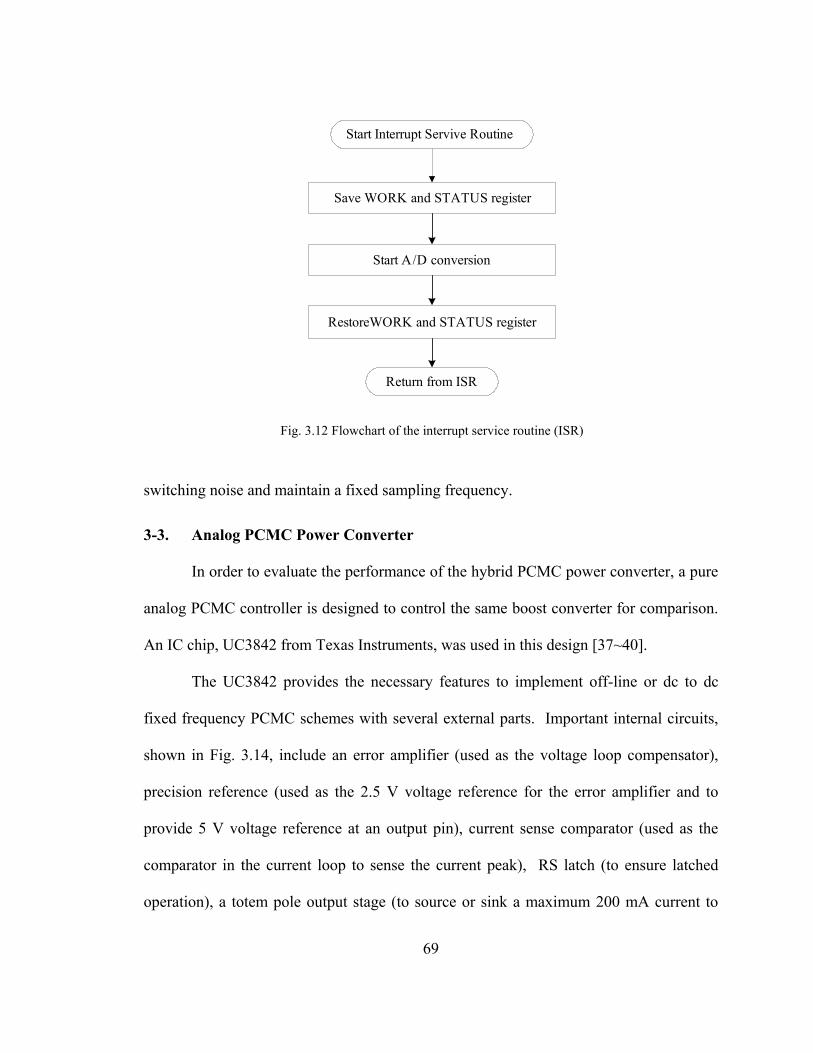
69
switching noise and maintain a fixed sampling frequency.
3-3. Analog PCMC Power Converter
In order to evaluate the performance of the hybrid PCMC power converter, a pure
analog PCMC controller is designed to control the same boost converter for comparison.
An IC chip, UC3842 from Texas Instruments, was used in this design [37~40].
The UC3842 provides the necessary features to implement off-line or dc to dc
fixed frequency PCMC schemes with several external parts. Important internal circuits,
shown in Fig. 3.14, include an error amplifier (used as the voltage loop compensator),
precision reference (used as the 2.5 V voltage reference for the error amplifier and to
provide 5 V voltage reference at an output pin), current sense comparator (used as the
comparator in the current loop to sense the current peak), RS latch (to ensure latched
operation), a totem pole output stage (to source or sink a maximum 200 mA current to
Save WORK and STATUS register
Start Interrupt Servive Routine
Start A/D conversion
RestoreWORK and STATUS register
Return from ISR
Fig. 3.12 Flowchart of the interrupt service routine (ISR)
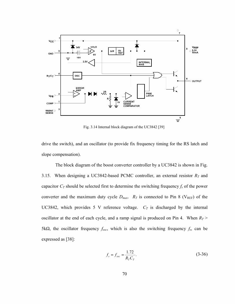
70
drive the switch), and an oscillator (to provide fix frequency timing for the RS latch and
slope compensation).
The block diagram of the boost converter controller by a UC3842 is shown in Fig.
3.15. When designing a UC3842-based PCMC controller, an external resistor RT and
capacitor CT should be selected first to determine the switching frequency fs of the power
converter and the maximum duty cycle Dmax. RT is connected to Pin 8 (VREF) of the
UC3842, which provides 5 V reference voltage. CT is discharged by the internal
oscillator at the end of each cycle, and a ramp signal is produced on Pin 4. When RT >
5kΩ, the oscillator frequency fosc, which is also the switching frequency fs, can be
expressed as [38]:
.72.1
TToscs CR
ff == (3-36)
Fig. 3.14 Internal block diagram of the UC3842 [39]

71
Equation (3-36) shows that a fixed witching frequency fs can be defined (156.25
kHz in this implementation) by selecting RTCT. RT and CT also determine the maximum
duty cycle Dmax. Dmax can be expressed by following equation [37]:
.1 sdmax ftD −= (3-37)
where td is the dead time, or discharge time of the capacitor. td is a function of RT and CT.
When RT is large enough (RT > 5kΩ), td is approximately directly determined by CT. The
relationship between td and CT is illustrated in Fig. 3.16 [37]. Thus, as long as fs and Dmax
are specified, CT can be obtained from Fig. 3.16 directly. For example, Dmax is set to 75%,
UC384215 V
VCC 71 Comp
2 VFB
4 RT/CT GND 5
Output 6RT
CT
Boost Converter
RC
L
Vin
PWM signal
+
Vo
-
VREF 83 Isense
+_
2.5 V150 kO
1 ORf
Ri
Rslope
R1
R2
C1
C2
R3
R4
C3
C4
Fig. 3.15 Block diagram of a boost converter controller by a UC3842
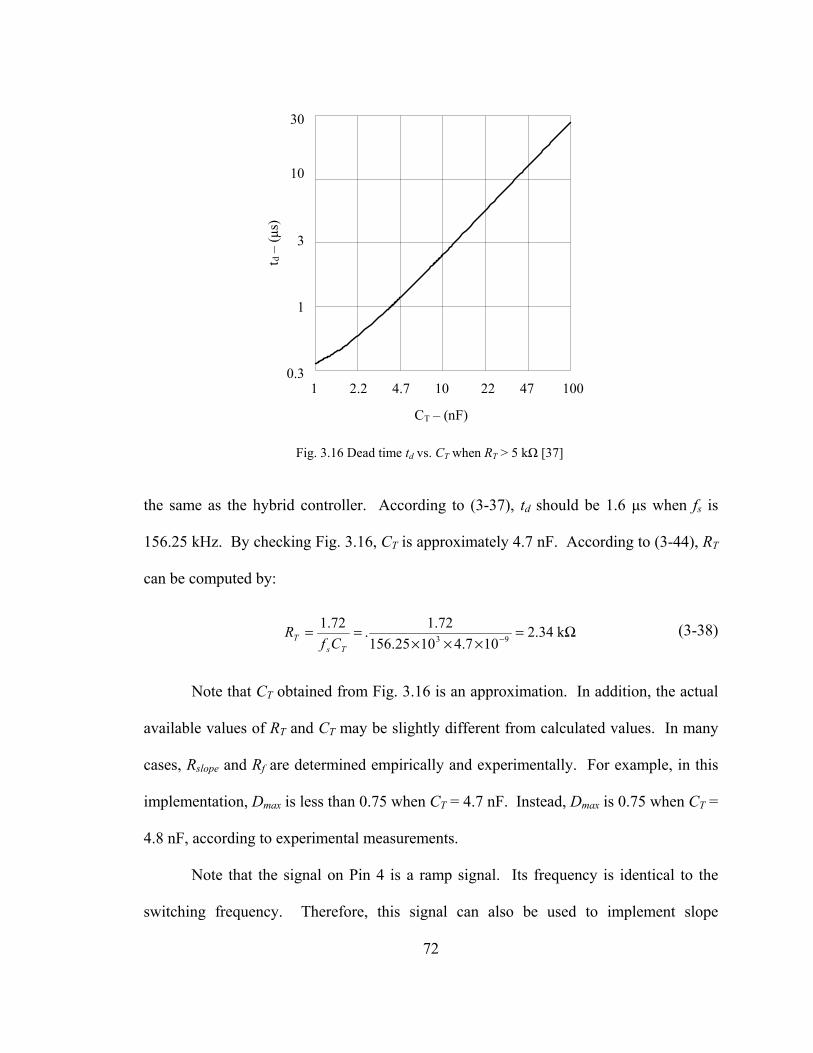
72
the same as the hybrid controller. According to (3-37), td should be 1.6 μs when fs is
156.25 kHz. By checking Fig. 3.16, CT is approximately 4.7 nF. According to (3-44), RT
can be computed by:
Ω=×××
== − k34.2107.41025.156
72.1.72.193
TsT Cf
R (3-38)
Note that CT obtained from Fig. 3.16 is an approximation. In addition, the actual
available values of RT and CT may be slightly different from calculated values. In many
cases, Rslope and Rf are determined empirically and experimentally. For example, in this
implementation, Dmax is less than 0.75 when CT = 4.7 nF. Instead, Dmax is 0.75 when CT =
4.8 nF, according to experimental measurements.
Note that the signal on Pin 4 is a ramp signal. Its frequency is identical to the
switching frequency. Therefore, this signal can also be used to implement slope
1 2.2 4.7 10 22 47 100
CT – (nF)
30
10
3
1
0.3
t d–
(µs)
Fig. 3.16 Dead time td vs. CT when RT > 5 kΩ [37]

73
compensation. Referring to Fig. 3.15, the ramp signal is added to the sensed inductor
current through a resistor Rslope, while the sensed current passes through another resistor
Rf. The values of Rf and Rslope determines the slope of the ramp signal. The calculation
method is similar to the hybrid controller, which is represented by (3-32) – (3-35).
However, since the ramp signal is also used to generate the switching frequency and to
set the maximum duty cycle, the current for slope compensation introduces an error into
the switching frequency and the maximum duty cycle. Therefore, it is required that Rslope
and Rf should be significantly larger than RT. Also, since the current sensing comparator
consumes up to 10 μA of bias current, large Rf may result in considerable error in the
measured the inductor current. Therefore, Rslope and Rf should be well below 100 kΩ.
In order to minimize the impact of the slope compensation circuit, the ramp signal
can amplified first by a transistor before it is added to the sensed current signal, as shown
in Fig. 3.17. By using an extra transistor amplifier, the slope compensation circuit has
very little effect on the switching frequency and maximum duty cycle. Also, smaller
values of Rslope and Rf can be used in the circuit.
4 RT/CT
RT
CT
3 Isense
Rf
RSlope
C3
~
~
~
5 V
To boost converter
UC3842C4
Fig. 3.17 A transistor is added in slope compensation circuit

74
Just as in the hybrid PCMC system, the voltage loop is also a PI controller, and
the equivalent gains are designed as close as possible to the digital counterpart. The PI
controller is constructed using the on-board error amplifier and three external
components (one capacitor C2 and two resistors R3 and R4). Referring to Fig. 3.15, the
transfer function of the PI controller can be expressed as:
⎟⎠⎞
⎜⎝⎛ +−=⎟⎟
⎠
⎞⎜⎜⎝
⎛+−=
sKK
sCRRRsG I
PPI .11)(233
4 (3-39)
3-4. Experimental Results
The specification of the boost converter used in experimental test is listed below:
― Nominal input voltage: 12 V
― Nominal output voltage: 28 V
― Switching frequency: 156.25 kHz:
― Nominal load: 50 Ω (0.56 A, 15.68 W)
― Operating condition: CCM
― Inductor: 257 μH
― Output capacitor: 35.42 µC
All the experimental waveforms in this chapter were recorded using a Tektronix
TDS 744A oscilloscope. AC coupling is utilized on the oscilloscope to remove the dc
level from all signals displayed on the oscilloscope. The block diagram of the boost
converter and its control system is shown in Fig. 3.18. The key component of the control
system is the PIC16C782 microcontroller. The voltage follower, which is constructed
using an external operational amplifier, is used to condition the voltage feedback. Since
the PWM output of the PIC16C782 is a 5 V level and cannot provide enough current to
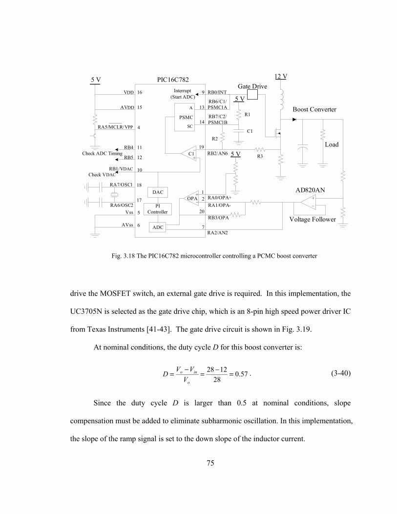
75
drive the MOSFET switch, an external gate drive is required. In this implementation, the
UC3705N is selected as the gate drive chip, which is an 8-pin high speed power driver IC
from Texas Instruments [41-43]. The gate drive circuit is shown in Fig. 3.19.
At nominal conditions, the duty cycle D for this boost converter is:
57.028
1228 =−=−
=o
ino
VVV
D . (3-40)
Since the duty cycle D is larger than 0.5 at nominal conditions, slope
compensation must be added to eliminate subharmonic oscillation. In this implementation,
the slope of the ramp signal is set to the down slope of the inductor current.
PIC16C782
ADC
PI Controller
A
PSMC
SC
DAC
+ _
12 V5 V
5 V
5 V
RB6/C1/PSMC1A
RB7/C2/PSMC1B
RB0/INT
RA0/OPA+
RB3/OPA
C1 RB2/AN6
RA1/OPA-
RA2/AN2
VDD
AVDD
_____RA5/MCLR/VPP
RB4
RB5Check ADC Timing
RB1/VDAC
RA7/OSC1
RA6/OSC2Vss
AVss
20
7
12
19
14
13
916
15
4
11
12
10
18
17
5
6
Check VDAC
AD820AN
Interrupt(Start ADC)
Gate Drive
Load
R1
R3
C1
+ _OPA
Voltage Follower
Boost Converter
R2
+_
Fig. 3.18 The PIC16C782 microcontroller controlling a PCMC boost converter

76
The primary issue in designing a power converter system is its ability to respond
to load or voltage changes and to adjust the output voltage to the nominal value.
According to the experimental results, the system can maintain an output voltage of 28 V
for a wide range of input voltages from 9.5 V to 25.5 V.
Ideally, the values of KP and KI’ are 0.7 and 0.0225, respectively. However, since
power-of-two arithmetic is employed, the values of KP and KI’ are 1/2 and 1/32 =
0.03125, respectively are selected; the system is a little bit under damped. For a load
change from 0.75 A to 0.187 A (Fig. 3.20), the system’s response time is roughly 2 ms to
reach steady state with small overshoot. The maximum transient error is about 1.2 V,
which is less than 5% of 28 V. In about 1 ms, the error reduces to around 0.1 V, which is
about 0.35% of 28V. The steady state error of the system is approximately zero.
When the load changes from 0.187 A to 0.75 A (Fig. 3.21), the response is similar.
The system spends roughly 2.5 ms to reach steady state with small overshoot. The
maximum transient error is 1.2 V. Within 1.2 ms, the error reduces to 0.1 V. The steady
INV. IN 7
1 Vs
2 VC
4 OUT PWD GND 5
Logic GND 6
N.I. IN 8
3 N/C
15 V
From the PIC16C782
10 O
0.1 O 1.2 kO
68 pF100 µF
Fig. 3.19 Gate drive circuit

77
Fig. 3.21 Transient response using the PIC16C782 when the load change is from 0.187 A to 0.75 A, and
KP = 1/2 and KI’ = 1/32. Output voltage: 500 mV/DIV; Time: 500 μs/DIV
Fig. 3.20 Transient response using the PIC16C782 when the load change is from 0.75 A to 0.187 A, and
KP = 1/2 and KI’ = 1/32. Output voltage: 500 mV/DIV; Time: 500 μs/DIV

78
state error of the system is approximately zero.
The step response for the voltage reference Vref (changing from 00h to 7Fh) is
shown in Fig. 3.22. The system can reach steady state in less than 2 ms with a small
overshoot of about 1.5 V, which is about 5% of 28 V.
The simulated results of the compensated system when KP = 1/2 and KI’ = 1/32
are depicted in Fig. 3.23. Compared to the uncompensated system, the gain at low
frequency and the gain margin are increased, but the phase margin is deceased to about
30° when the load is 0.187 A. By using the analog network analyzer, the frequency
response of the compensated system are recorded experimentally and then plotted in
MATLAB, as shown in Fig. 3.24. The experimental responses in Fig. 3.24 match the
simulated responses in Fig. 3.23 well with small errors.
Fig. 3.22 Step response using the PIC16C782 when the load is 0.56 A. Output voltage: 5 V/DIV; Time: 500 μs/DIV

79
102 103 104
-20
0
20
40
60Bode Plot According to Experimental Data
0.187 A0.56 A0.75 A
102 103 104-350
-300
-250
-200
-150
-100
-50
0
Fig. 3.24 Experimental responses of compensated PCMC boost converter
using digital PI controller for different load
Bode Diagram
Frequency (rad/sec)
Phas
e (d
eg)
Mag
nitu
de (d
B)
-40
-20
0
20
40
60
80
0.187 A0.56 A0.75 A
102
103
104
105
-540
-450
-360
-270
-180
-90
Fig. 3.23 Simulation of compensated PCMC boost converter using PI controller for different load

80
If KP = 1/2 and KI’ = 1/64 = 0.015625 are selected, the system is a little bit over
damped, so the speed of response is a little slower than when KI’ = 1/32 = 0.03125. For a
load change from 0.75 A to 0.187 A (Fig. 3.25), the system’s response time is roughly 2.8
ms to reach steady state without any overshoot. When the load changes from 0.187 A to
0.75 A (Fig. 3.26), the response is roughly 3 ms without any overshoot. In both cases,
the maximum transient error is about 1.3 V, which is less than 5% of 28 V, and the steady
state error of the system is approximately zero.
Fig. 3.20 – Fig. 3.26 indicate that the power-of-two algorithm can achieve
satisfactory results. When higher resolution for the gains is required, two or more power-
of-two numbers can be added together. For example, by adding 1/2 and 1/4 of the
original number together, a gain of 3/4 can be obtained.
Fig. 3.25 Transient response using the PIC16C782 when the load change is from 0.75 A to 0.187 A, and
KP = 1/2 and KI’ = 1/64. Output voltage: 500 mV/DIV; Time: 500 μs/DIV

81
The analog controller using the UC3842 from Texas Instruments is tested on the
same boost converter for comparison. This analog controller also contains a PI controller
in its voltage loop with the equivalent gains as close as possible to the digital counterpart.
Fig. 3.27 and Fig. 3.28 illustrate the transient responses of the analog controller. When
load changes from 0.75 A to 0.187 A or vice versa, the system’s response time is less
than 1.5 ms to reach steady state with a maximum transient error less than 0.9 V.
Therefore, the analog controller performs a little bit better than the digital controller. On
the other hand, the digital controller demonstrates some advantages over analog
controller. According to the experimental results, the analog controller remains stable for
input voltages up to 19 V. The switching frequency alters a little bit when the load
changes due to the slope compensation circuit.
Fig. 3.26 Transient response using the PIC16C782 when the load change is from 0.187 A to 0.75 A, and
KP = 1/2 and KI’ = 1/64. Output voltage: 500 mV/DIV; Time: 500 μs/DIV

82
Fig. 3.27 Transient response using analog controller when the load change is from 0.75 A to 0.187 A.
Output voltage: 200 mV/DIV; Time: 200 μs/DIV
Fig. 3.28 Transient response using analog controller when the load change is from 0.187 A to 0.75 A.
Output voltage: 200 mV/DIV; Time: 200 μs/DIV

83
3-5. Conclusion
Presented in this chapter is the practical design of a microcontroller-based PCMC
boost converter. The PIC16C782 provides a one-chip solution for a PCMC DC-DC
converter with the exception of a voltage follower. The on-board peripherals of the
PIC16C782 are suitable and critical in designing the PCMC dc-dc converter. The
PIC16C82 also provides the mechanism to implement slope compensation, which allows
PCMC DC-DC converters to operate for duty cycles greater than 50%. Practical issues in
designing a microcontroller-based peak CMC boost converter are briefly discussed.
Experimental results are presented, and encouragingly demonstrate the
performance that a microcontroller-based PCMC DC–DC converter can achieve. An
analog controller based on a UC3842 is also designed for comparison.
Though this microcontroller-based PCMC system is designed for a boost
converter, it can be directly applied to all major converters with very minor modifications.

84
CHAPTER 4
MICROCONTROLLER-BASED AVERAGE CURRENT-MODE CONTROL
This chapter presents a practical implementation of average current-mode control
for a boost converter using an 8-bit microcontroller. The design principles of the hybrid
control method used in PCMC power converter systems are extended to an ACMC boost
converter, which proves that the hybrid method can be used in both PAMC and ACMC
power converter systems. This microcontroller-based hybrid ACMC controller has been
compared to a pure analog ACMC controller based on a UC3886 from Texas Instruments.
4-1. Modiling Average Current-Mode Control
The difference between ACMC and PCMC is that a current amplifier is inserted
in the current loop for ACMC. The complete current loop is shown in Fig. 4.1, in which
Li is the inductor current, Ri is linear gain of the current-sense network, cv is the control
reference from the voltage loop, Vm is the peak-to-peak voltage of the ramp signal, Sn is
OPA
Cfp
CfzRf RI
+ _
vc
RiiL
+ _
Vm
d
ComparatorCurrent Amplifier
^^
^
S n
Sn ’
Fig. 4.1 Typical current loop compensator
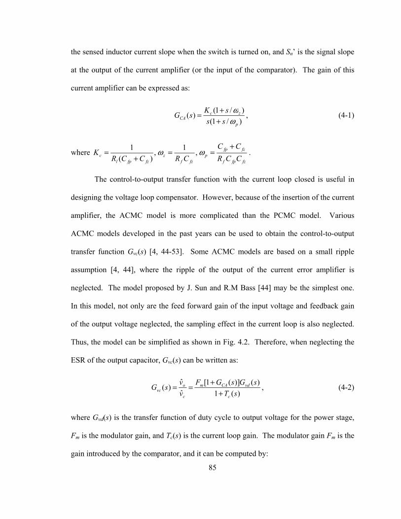
85
the sensed inductor current slope when the switch is turned on, and Sn’ is the signal slope
at the output of the current amplifier (or the input of the comparator). The gain of this
current amplifier can be expressed as:
)/1()/1()(
p
zcCA ss
sKsGωω
++= , (4-1)
where fzfpf
fzfpp
fzfz
fzfplc CCR
CCCRCCR
K+
==+
= ωω ,1,)(
1 .
The control-to-output transfer function with the current loop closed is useful in
designing the voltage loop compensator. However, because of the insertion of the current
amplifier, the ACMC model is more complicated than the PCMC model. Various
ACMC models developed in the past years can be used to obtain the control-to-output
transfer function Gvc(s) [4, 44-53]. Some ACMC models are based on a small ripple
assumption [4, 44], where the ripple of the output of the current error amplifier is
neglected. The model proposed by J. Sun and R.M Bass [44] may be the simplest one.
In this model, not only are the feed forward gain of the input voltage and feedback gain
of the output voltage neglected, the sampling effect in the current loop is also neglected.
Thus, the model can be simplified as shown in Fig. 4.2. Therefore, when neglecting the
ESR of the output capacitor, Gvc(s) can be written as:
)(1)()](1[
ˆˆ
)(sT
sGsGFvvsG
c
vdCAm
c
ovc +
+== , (4-2)
where Gvd(s) is the transfer function of duty cycle to output voltage for the power stage,
Fm is the modulator gain, and Tc(s) is the current loop gain. The modulator gain Fm is the
gain introduced by the comparator, and it can be computed by:

86
mm V
F 1= . (4-3)
The current loop gain Tc(s) is:
)()()( sGsGFRsT idCAmic = . (4-4)
where Gid(s) is the duty cycle to inductor current transfer function. Although this model
is simple, it neglects the feedback and the feedforward terms, the sampling effect in the
current loop ripple, as well as the ripple in the output of the current amplifier. When the
inductor and capacitor are not large enough, the current ripple in the inductor and voltage
ripple at the output may be too large to ignore. In addition, when the gain of the current
amplifier is high, the model is inaccurate. All these may lead to an inaccurate design.
Therefore, many models have attempted to include the effect of inductor ripple and
sampling effect on the dynamics of an ACMC converter [45-53].
T. Suntio, etal. [46-47] expended the previous model by including the dynamic
effects of inductor current ripple, and the resulting control-to-output transfer function is:
Power Stage Gvd(s), Gid(s)
GCA(s)–
+
vg^
vc^
vo^
iL
Fm Ri
d
Fig. 4.2 Sun and Bass’ small signal model for an ACMC converter [44]

87
)()(1)()](1[
ˆˆ
)(sTsT
sGsGFvvsG
vc
vdCAm
c
ovc ++
+== , (4-5)
where Tv(s) is voltage loop gain. Tv(s) is computed by:
)()( 0 sGqFsT vdmv = , (4-6)
where q0 is a coefficient depending on the topology. Compared to (4-2), an extra voltage
loop gain Tv(s) is added. The expression of the modulator gain Fm is also different, since
one more term is added in the denominator:
s
olm
m
LfDDVKV
F
2)'(
1−+
= , (4-7)
where Kl is an coefficient derived from the current loop compensator, and can be
expressed as (referring to Fig. 4.1):
)( fzfpl
fzfl CCR
CRK
+= . (4-8)
For a boost converter, q0 can be expressed as:
s
l
LfDDKq
2'
0 = . (4-9)
Since this model includes the inductor ripple effect, it is more accurate at the
expense of more complicated expressions.
In [52-53], another ACMC small-signal model is derived utilizing previous results
based on Ridley’s PCMC model [23-25]. This model is illustrated in Fig. 4.3, Kf is the
feed-forward gain, Kr is the feedback gain, and He(s) is the sampling gain. Gs(s) and Gp(s)

88
are derived from the current amplifier, and can be computed by (referring to Fig. 4.1):
s
sKsG z
c
s
⎟⎟⎠
⎞⎜⎜⎝
⎛+
=ω
1)( , (4-10)
⎟⎟⎠
⎞⎜⎜⎝
⎛+
=
p
ps
sG
ω1
1)( , (4-11)
where Kc, ωp and ωz are identical to the values in (4-1).
The sampling gain He(s) and the modulator gain Fm can be computed by:
Power Stage Gvd(s), Gid(s)
He(s)
+
vg^
vc^
vo^
iL
Fm
Ri
dKr
Gs(s)
Gp(s)
Kf
+ +
+
–
Fig. 4.3 Tang’s small-signal model for ACMC converter [52-53]

89
2
2
1)(nzn
es
QssH
ωω++≅ , (4-12)
sn T
πω = , (4-13)
π2−=zQ , (4-14)
snem TSS
F)(
1'+
= , (4-15)
where Se is the slope of the external ramp, Sn’ is the modified slope of the inductor current
waveform, as illustrated in Fig. 4.1. Sn’ can be computed by [52-53]:
( )⎥⎥⎦
⎤
⎢⎢⎣
⎡−⎟
⎟⎠
⎞⎜⎜⎝
⎛−+= − spDT
pzsncn eDTSKS ω
ωω111' . (4-16)
Feedforward and feedback gain terms Kf and Kr are different for different types of
converters. Table 4-1 lists Kf and Kr for three basic types of converters, where:
( )γαβαξ /1 sDTs eDT −−+= , (4-17)
( )γαβγαβαζ /2
12
)(sDT
ss eDTDT −−−+= , (4-18)
Table 4.1 Feedforward and feedback gains for ACMC [52-53]
Buck Boost Buck-Boost
Kf ζξL
RLTDD is
22−
′− ζξ
LR
LTD is
22−
′− ξ
LTDD s
2′
−
Kr ζξL
RLTD is
22−
′− ξ
LTD s
2′
− ξLTD s
2′
−

90
)(1
fzfpf CCR +=α , (4-19)
)(
2
fzfp
fzf
CCCR+
=β , (4-20)
)( fzfp
fzfpf
CCCCR
+=γ . (4-21)
According to Fig. 4.3, the control-to-output transfer function can be expressed as:
)()()()(1)()()(
ˆˆ
)(sGFKsGsGsHFR
sGsGsGFvvsG
vdmridsemi
vdspm
c
ovc −+
== . (4-22)
This model uses the sampling gain He(s) directly from the PCMC model without
strict derivation. Therefore, it can be inaccurate if the gain of the current amplifier is
high. Also, this model contains a nonlinear expression for the modulator gain, which
adds complexity to the model.
The Bode plots of Gvc(s) of the three models for the ACMC boost converter used
in this implementation are plotted in Fig. 4.4. The measured transfer function is also
plotted for comparison. According to Fig. 4.4, the three models can provide very
accurate predictions at low frequency. However, all of them deviate from the
measurement at above half of the switching frequency, while Tang’s model is relatively
more accurate. Since the actual Gvc(s) has an infinite number of poles, all of the
theoretical models are based on some approximations. Therefore, Gvc(s) from the
experimental measurement is always the first choice when it is possible, as in this
implementation.

91
4-2. System Design
4-2-1. System overview
The block diagram for the microcontroller-based hybrid ACMC boost converter is
shown in Fig. 4.5. In the current loop, a current amplifier, which is constructed using the
on-board OPA module, is inserted to obtain the average value of the inductor current, so
the output of the current amplifier is proportional to the average inductor current with
some ripple. Its current reference is calculated in software using a PI compensator.
Using the on-chip analog comparator C1, the amplified error from the current amplifier
OPA is compared to a sawtooth reference waveform produced by the PSMC module. A
pulse is generated when they are equal, and is sent to the PSMC module to generate a
-40
-20
0
20
40
60
Mag
nitu
de (d
B)
102
103
104
105
0
90
180
270
360
Phas
e (d
eg)
Comparison of the control-to-output transfer functions of the ACMC boost converter
Frequency (rad/sec)
Experimetnal DataJ. Sun's modelT. Suntio's modelW. Tang's model
Fig. 4.4 Comparison of the ACMC models
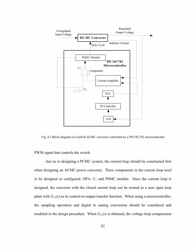
92
PWM signal that controls the switch.
Just as in designing a PCMC system, the current loop should be constructed first
when designing an ACMC power converter. Three components in the current loop need
to be designed or configured: OPA, C1 and PSMC module. Once the current loop is
designed, the converter with the closed current loop can be treated as a new open loop
plant with Gvc(s) as its control-to-output transfer function. When using a microcontroller,
the sampling operation and digital to analog conversion should be considered and
modeled in the design procedure. When Gvc(s) is obtained, the voltage loop compensator
DC-DC Converter
D/A
+ _
Vm
Comparator
PSMC Module
Unregulated Input Voltage
Regulated Output Voltage
Inductor CurrentDuty Cycle
PIC16C782Microcontroller
Current Amplifier
PI Controller
A/D
C1
Fig. 4.5 Block diagram of a hybrid ACMC converter controlled by a PIC16C782 microcontroller

93
Gc(z) can be designed based on Gvc(s) as a typical digital control system. Thus, the block
diagram of the ACMC system is the identical to the PCMC system shown in Fig. 3.5.
The hidden difference is that they have different control to output transfer function Gvc(s).
In this implementation, the operating specifications and circuit parameters are
listed as following:
― Nominal input voltage: 12V
― Nominal output voltage: 28V
― Switching frequency: 156.25kHz:
― Nominal load: 50Ω (0.56A, 15.68W)
― Operating mode: CCM
― Inductor: 257 µH
― Output capacitor: 57.35μF
4-2-2. Current loop design
The complete current loop realized on the PIC16C782 is shown in Fig. 4.6. Since
both the OPA module and the comparator C1 are analog peripherals inside the
microcontroller, the current loop is the same as a traditional analog ACMC case.
Therefore, no complex algorithm is required to estimate the inductor current.
The current amplifier in the current loop can be designed by using the on-board
analog operational amplifier module (OPA module) with several external capacitors and
resistors, as illustrated in Fig. 4.6. When designing the current amplifier, its gain should
be chosen first. Since the down slope of the amplified inductor current error must not
exceed the slope of the external ramp, there is an upper limitation on the current amplifier
gain GCA at the switching frequency fs. This indirectly establishes the maximum current

94
loop gain and crossover frequency. GCA is approximately Rf/Rl at the switching frequency,
and can be expressed by [4, 44 and 48]:
⎪⎭
⎪⎬⎫
⎪⎩
⎪⎨⎧
<≅io
sm
ig
sm
l
fCA RV
LfVRV
LfVRR
G ,2min . (4-23)
Equations (4-1) and (4-23) set the criteria to choose Rf and Rl. According to
desired locations of the pole and zero, capacitor values can be selected. In this
implementation, the zero ωz is placed at one-half of ω0, which is given by LC/10 =ω ,
to maximize the current loop crossover frequency. The high frequency pole ωp, is placed
at one-half of the switching frequency fs to filter out the switching frequency ripple. The
following steps are employed to design the current amplifier:
1. Compute Rf and Rl such that the current amplifier has a smaller gain than
5V
R
C
VDD
PIC16C782
vm(t)
Comparator C1
+ _
~
R2
Rl
Ri
G
PSMCModule
RB6/C1/PSMC1A
RB7/C2/PSMC1B
RB2/AN6
RB3/OPA
Cfp
CfzRf
RA3/AN3
+ _
RA0/OPA+
RA1/OPA-vca(t)
vca(t)
vc(t)
OPA
Fig. 4.6 Current loop for hybrid ACMC power converter realized on a PIC16C782

95
the maximum gain allowed at switching frequency:
38.181.028
108.1091025.1563 63
max =×
××××==≤−
io
smCA
l
f
RVLfVG
RR
. (4-24)
Ideally, Vm should be 5 V (which is the supply voltage of the microcontroller) to
achieve the maximum gain. However, vm is generated by an RC network, which will be
discussed in detail later, so Vm has to be set below 5 V to ensure an approximate linear
ramp signal. Select Rf = 91 kΩ and Rl = 5.1 kΩ, so 8.17=l
f
RR
, which satisfies the
requirement in (4-24) that 38.18≤l
f
RR
.
3. Compute the resonant frequency ω0 of the power stage:
rad/s106.121035.57108.109/1/1 3660 ×=×××== −−LCω . (4-25)
4. Compute Cfz according to the location of the zero ωz. In this
implementation, ωz is placed at one-half of ω0:
21 0ωω ==
zffz CR
. (4-26)
pF1500F1074.1106.121091
22 933
0
≅×=×××
== −
ωfzf R
C . (4-27)
The reason that Cfz is selected 1500 pF instead of 1740 pF is that this is the closest
available value to 1740 pF. Thus, the zero is actually at:
s/rad103.71015001091
1 3123 ×=
×××= −zω . (4-28)
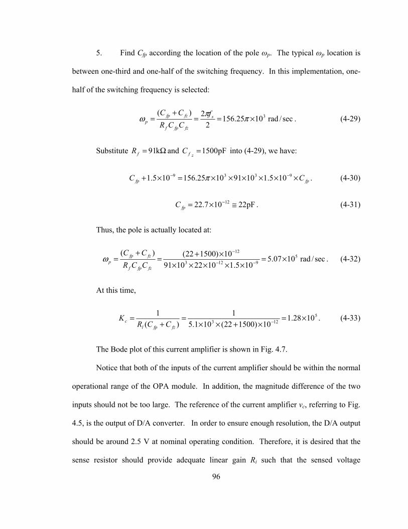
96
5. Find Cfp according the location of the pole ωp. The typical ωp location is
between one-third and one-half of the switching frequency. In this implementation, one-
half of the switching frequency is selected:
sec/rad1025.1562
2)( 3×==+
= ππω s
fzfpf
fzfpp
fCCRCC
. (4-29)
Substitute Ω= k91fR and pF1500=zfC into (4-29), we have:
fpfp CC ××××××=×+ −− 9339 105.110911025.156105.1 π . (4-30)
pF22107.22 12 ≅×= −fpC . (4-31)
Thus, the pole is actually located at:
sec/rad1007.5105.110221091
10)150022()( 59123
12
×=×××××
×+=+
= −−
−
fzfpf
fzfpp CCR
CCω . (4-32)
At this time,
5123 1028.1
10)150022(101.51
)(1 ×=
×+××=
+= −
fzfplc CCR
K . (4-33)
The Bode plot of this current amplifier is shown in Fig. 4.7.
Notice that both of the inputs of the current amplifier should be within the normal
operational range of the OPA module. In addition, the magnitude difference of the two
inputs should not be too large. The reference of the current amplifier vc, referring to Fig.
4.5, is the output of D/A converter. In order to ensure enough resolution, the D/A output
should be around 2.5 V at nominal operating condition. Therefore, it is desired that the
sense resistor should provide adequate linear gain Ri such that the sensed voltage
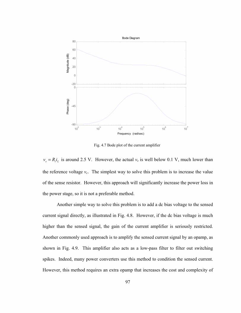
97
Lis iRv = is around 2.5 V. However, the actual vs is well below 0.1 V, much lower than
the reference voltage vc. The simplest way to solve this problem is to increase the value
of the sense resistor. However, this approach will significantly increase the power loss in
the power stage, so it is not a preferable method.
Another simple way to solve this problem is to add a dc bias voltage to the sensed
current signal directly, as illustrated in Fig. 4.8. However, if the dc bias voltage is much
higher than the sensed signal, the gain of the current amplifier is seriously restricted.
Another commonly used approach is to amplify the sensed current signal by an opamp, as
shown in Fig. 4.9. This amplifier also acts as a low-pass filter to filter out switching
spikes. Indeed, many power converters use this method to condition the sensed current.
However, this method requires an extra opamp that increases the cost and complexity of
-20
0
20
40
60
80
Mag
nitu
de (d
B)
102
103
104
105
106
107
-90
-45
0
Phas
e (d
eg)
Bode Diagram
Frequency (rad/sec)
Fig. 4.7 Bode plot of the current amplifier

98
the circuit.
In this implementation, instead of manipulating the sensed current signal, the
current reference of the current amplifier is modified. As shown in Fig. 4.10, the D/A
output, instead of being sent directly to the current amplifier, is connected to a voltage
divider. This method scales down the D/A output, such that it is compatible with the low
sensed current signal. This method is simple and low-cost, but it can effectively solve the
problem.
Since there is no internal analog path between the OPA module and the on-board
comparator C1, the output of the current amplifier vca is sent out of the PIC16C782
C
R2R1
vs=RiiL + _
Ri
~
To current amplifier
Fig. 4.9 Sensed current signal is amplified by an opamp
R1vs=RiiL
Ri
R2
R3
C
5V
~
To current amplifier
Fig. 4.8 Sensed current signal is biased by a dc voltage

99
through an analog IO port, and then is sent to C1 through another analog IO port. The
waveforms at C1 inputs are shown in Fig. 4.11, where vm is the ramp signal at the C1
negative input. It can be seen that vca has ripple, which makes the design of the current
loop more complicated.
In the hybrid PCMC scheme, a ramp signal for slope compensation is generated
by the PSMC module and an external RC network. In the hybrid ACMC scheme,
although slope compensation is eliminated, the ramp signal vm is still needed as the
reference for the comparator. For a fixed supply voltage (5 V in this implementation),
referring to Fig. 4.6, vm is directly defined by R and C. For an RC circuit, the time
D/A
R2
To current amplifierR1
Fig. 4.10 D/A output is scaled down by a voltage divider
D = Duty Cycle
T = Switching Cycle
1 16T
vca
vm
Fig. 4.11 The waveforms at C1 inputs
100
constant is τ = RC, and R and C can be selected by:
55ln
55)( /
m
RCtm v
tRCetv −−=⇒−= − . (4-34)
When designing the RC network to generate vm, the peak value of vm, referred to
as Vm, should be chosen as high as possible, according to (4-23). However, the linearity
of vm should be considered. Therefore, vm should not be close to 5 V at any possible duty
cycle. When the maximum duty cycle is specified, vm should be below 5 V at maximum
duty cycle. For example, in this implementation, let vm equal 3.8 V at 75% duty cycle.
Since fs = 156.25 kHz, so Ts = 6.4 μs. Thus,
s10363.3
58.35ln
75.0104.6 66
−−
×=−
××−=RC . (4-35)
Choose C = 100 pF, then R = 33.63 kΩ ≈ 33 kΩ. Based experimental
measurement, the actual value of vm reaches 3.4 V at 75% duty cycle (Dmax, maximum
duty cycle). The equivalent Vm is:
V6.475.04.3)( ===
= sTmaxDtmax
mm D
tvV . (4-36)
4-2-3. Voltage loop design
Once the current loop is designed, the converter with the closed current loop can
be treated as a new open loop plant with Gvc(s) as its control-to-output transfer function.
The voltage loop compensator Gc(z) can be designed based on Gvc(s).
In order to get higher A/D resolution, just as in the hybrid PCMC system, a level-
101
shift circuit was designed such that the A/D result represents a “windowed” range of the
output voltage around the nominal value. In this implementation, the “window” is in the
range of 25.67 V and 30.33 V for a 28 V nominal output voltage. The level shifter can be
built from an external operational amplifier with several external resistors. A voltage
buffer (voltage follower) is used to ensure accurate measurement of the output voltage.
The circuit is similar to that of the hybrid PCMC converter (Fig. 3.4). The main
difference is that, in the hybrid PCMC converter, the level-shift circuit is constructed
using the on-board opamp OPA module. However, in the ACMC system, since the OPA
module is used as the current amplifier, two external opamps, although they are
integrated in one IC chip, are used to construct the level-shift circuit and the voltage
buffer.
Due to the limited number of analog I/O ports of the PIC16C782, the full-range
output voltage is not measured. However, this restriction does not degrade the
performance of the controller because the output voltage variation during normal
operation is always inside the windowed range even under large disturbances. When the
converter starts up, the output voltage is out of the “windowed” range, and an overshoot
may occur. At this time, a full-range measurement may be required. However, an
appropriately designed voltage loop compensator can limit the overshoot to a small value,
which has been verified by checking the step response of the ACMC boost converter. In
addition, a soft start can be achieved easily by adding extra code before the software
enters normal operating mode.
In this implementation, the voltage loop compensator Gc(z), just as the PCMC
system described in Chapter 3, is a digital PI controller, and the design procedure is also
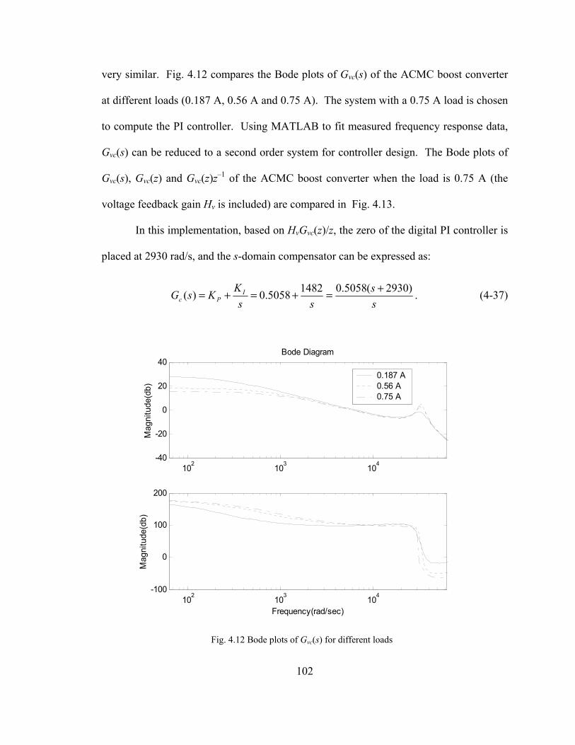
102
very similar. Fig. 4.12 compares the Bode plots of Gvc(s) of the ACMC boost converter
at different loads (0.187 A, 0.56 A and 0.75 A). The system with a 0.75 A load is chosen
to compute the PI controller. Using MATLAB to fit measured frequency response data,
Gvc(s) can be reduced to a second order system for controller design. The Bode plots of
Gvc(s), Gvc(z) and Gvc(z)z–1 of the ACMC boost converter when the load is 0.75 A (the
voltage feedback gain Hv is included) are compared in Fig. 4.13.
In this implementation, based on HvGvc(z)/z, the zero of the digital PI controller is
placed at 2930 rad/s, and the s-domain compensator can be expressed as:
ss
ssKKsG I
Pc)2930(5058.014825058.0)( +=+=+= . (4-37)
102 103 104-40
-20
0
20
40Bode Diagram
Mag
nitu
de(d
b)
0.187 A0.56 A0.75 A
102 103 104-100
0
100
200
Mag
nitu
de(d
b)
Frequency(rad/sec)
Fig. 4.12 Bode plots of Gvc(s) for different loads

103
where KP is the proportional gain and KI is the integral gain. The s-domain PI controller
is then converted to a z-domain transfer function as:
103794.05058.0
11)(
'
−+=
−+=
−+=
zz
zzKK
zzTKKzG I
PsI
Pc . (4-38)
According to Gc(z), the control effort vc(k) can be computed using the following
difference equation:
∑∑==
+=+=k
j
k
jIPc jejeKKkv
00
' )(03794.05058.0)()( , (4-39)
where e(k) is the error signal which is computed digitally by comparing the ADC result
of the output voltage vo(k) and a voltage reference Vref(k). Vref(k) is fixed at 7Fh, which
-40
-30
-20
-10
0
10
20
Mag
nitu
de (d
B)
102
103
104
-180
0
180
360
Phas
e (d
eg)
Bode Diagram
Frequency (rad/sec)
HvGvc(s)HvGvc(z)HvGvc(z)/z
Fig. 4.13 Bode plots of ACMC boost converter when the load is 0.75 A

104
represents a fixed nominal output voltage.
Power-of-two arithmetic is employed in this implementation. Therefore, KP =
0.5, 'IK = 1/32 = 0.03125 are selected. The software keeps track of the sign by storing
the error sign in a flag bit.
The DAC module inside the PIC16C782 is used to convert the output of the
digital PI controller into an analog signal vc(t). The DAC reference voltage can only be 5
V or 3.072 V; other reference voltages are not practical in this implementation because of
restrictions on the I/O pins. As discussed in Section 4-2-2, a voltage divider made of two
resistors is used to scale down the DAC output. This voltage divider introduces an extra
gain to the voltage loop, which can provide more flexibility to design the PI controller
and compensate the drawback of power-of-two arithmetic by adjusting the gain of the
voltage divider, and hence adjusting KP and 'IK .
In this implementation, the maximum duty cycle Dmax is set to be 75%.
4-3. Analog ACMC Power Converter
For comparison, an analog controller using an UC3886 from Texas Instruments
[54-56] was designed to control the same boost converter.
The UC3886 was developed to implement dc to dc power converter system with
ACMC. As illustrated in Fig. 4.14, this 16-pin IC chip internally includes one PWM
comparator, three amplifiers (voltage amplifier, current amplifier and current sense
amplifier), precision reference (trimmed 5 V reference at an output pin), RS latch (to
ensure latched operation), 1.5 A totem pole output stage, and an oscillator (to provide fix
frequency timing for RS latch and slope compensation). The current sense amplifier

105
inside the UC3886 can amplify the sensed current, and eliminate the need for external
waveform synthesis circuitry. Using a UC3886, a one-chip solution for the ACMC
controller, including input conditioning controller and gate drive, can be achieved. In
addition to the basic ACMC functions, a UC3886 also has comprehensive supplementary
functions, such as undervoltage lockout, short circuit protection, current limit for high
load and soft start.
Since both of the current loops using the PIC16C782 and the UC3886 are
implemented using analog circuitry, the design procedures for the current loops using the
UC3886 were similar. In the voltage loop, an analog PI controller was implemented.
This analog PI controller contains gains equivalent to the digital counterparts as close as
possible.
Fig. 4.14 Internal block diagram of UC3886 [54]
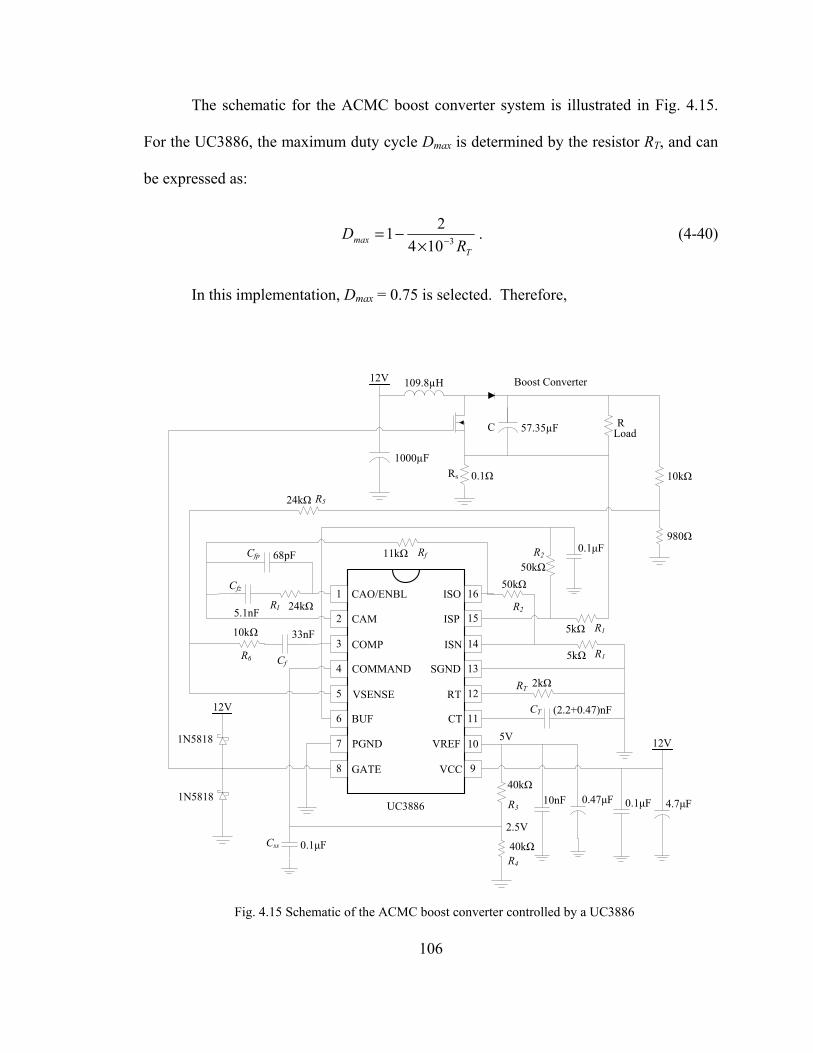
106
The schematic for the ACMC boost converter system is illustrated in Fig. 4.15.
For the UC3886, the maximum duty cycle Dmax is determined by the resistor RT, and can
be expressed as:
Tmax R
D 310421 −×
−= . (4-40)
In this implementation, Dmax = 0.75 is selected. Therefore,
12V
Load
Boost Converter
Rs
RC
1
2
3
4
5
6
7
8
16
15
14
13
12
11
10
9
CAO/ENBL ISO
CAM ISP
COMP ISN
COMMAND SGND
VSENSE RT
BUF CT
PGND VREF
GATE VCC
12V
1N5818
1N5818
12V
109.8µH
57.35µF
0.1Ω
0.1μF 4.7μF
1000µF
68pF
5.1nF 24kΩ
11kΩ
24kΩ
10kΩ 33nF
50kΩ50kΩ
5kΩ
5kΩ
2kΩ
(2.2+0.47)nF
40kΩ
40kΩ
10nF 0.47μFUC3886
10kΩ
980Ω
5V
RT
CT
R1
R1
R2
R2
0.1μF
R3
R4
2.5V
Rf
RI
Cfp
Cfz
R5
R6 Cf
0.1μFCss
Fig. 4.15 Schematic of the ACMC boost converter controlled by a UC3886

107
Ω=−××
=−×
= −− k2)75.01(104
2)1(104
23
max3 D
RT . (4-41)
The switching frequency is found by following equation:
23
3
1048.1)2104(2
TT
Ts RC
Rf −
−
××−×= . (4-42)
Substitute fs = 156.25 kHz and RT = 2 kΩ into (4-42), CT is obtained:
nF)47.02.2(F1067.2)102(1025.1561048.1
)2102104(2 92333
33
+=×=××××××
−×××= −−
−
TC . (4-43)
The current sense amplifier (CSA) inside UC3886 can provide adequate gain and
offset to the sensed inductor current. The gain GCSA of CSA must be larger than 5 (14dB),
otherwise it is not stable. In addition, GCSA has an upper limit:
)dB24(161025.156
105.2105.23
66
=×
×=×≤s
CSA fG . (4-44)
GCSA is given by the resistors R1 and R2, and is set to be 10 in this implementation:
101
2 ==RRGCSA . (4-45)
Let R1 = 5 kΩ, and R2 = 50 kΩ. Then, the CSA output VISO is expressed as:
iLCSASENSEBUFISO RIGVVV 105.2 +=+= , (4-46)
where VSENSE is the output voltage feedback at Pin VSENSE, and VBUF is dc bias voltage,
and is set to 2.5 V in this implementation. Indeed, VBUF equals to Vcommand, which is set
by resistors R3 and R4. In this implementation, R3 = R4 = 40 kΩ, such that VBUF = 2.5 V.
Vcommand is also the reference of the voltage amplifier.

108
The ramp signal vm used as the reference of the comparator is generated internally
by the on-board oscillator. The signal vm rings from 1 V to 2.8 V. Therefore, Δvm, the
peak-to-peak voltage of vm, equals to 2.8 – 1 = 1.8 V. Thus, the equivalent full-cycle
peak-to-peak voltage Vm can be computed as:
V12.285.0
)18.2()( =−=Δ== sTmaxDtmax
mm D
tvV . (4-47)
According to (4-23), the ratio of Rf and Rl is defined by the maximum gain of the
current amplifier (CA):
3.1101.028
108.1091025.15612.2)(
63
max =××
××××==≤−
CSAio
smCA
l
f
GRVLfVG
RR
. (4-48)
Equation (4-48) shows that the CA gain is as low as 1.3. This is because the
linear gain to the inductor current has been increased by CSA. In other words, the upper
limit of the CA gain is traded with the CSA gain. However, Vm is only 2.12 V. vm is in
the range of 1 V and 2.8 V, which is a specification of the UC3886, and cannot be
changed. Therefore, the only way to further increase Vm (equivalent to increase the slope
of the ramp signal) is to further decrease the maximum duty cycle below 75%, which is
undesirable in this implementation. Compared with Vm = 4.6 V in the PIC16C782 system,
this restriction further limits GCAmax.
Select Rf = 31 kΩ and Rl = 24 kΩ. Thus:
3.129.1kΩ24kΩ31
max =≤== CAl
f GRR
. (4-49)
According to (4-25), the resonant frequency ω0 of the power stage is 12.6×10³

109
rad/s. Place the zero of CA ωz at one-half of ω0 by setting Cfz:
nF1.5F1012.51031106.125.0
11 933 ≅×=
××××== −
fzfz R
Cω
. (4-50)
Cfp is selected based on the location of the pole of CA ωp, which is at one-half of
the switching frequency here. Substitute Rf = 31 kΩ and Cfz = 5.1 nF into (4-29), the
following equation is obtained:
s/rad1025.156101.51031
)101.5( 393
9
×=××××+
−
−
πfp
fp
CC
. (4-51)
Solve (4-51), Cfp is calculated to be 66.6 pF, and a 68 pF capacitor is selected.
The voltage amplifier compares the output voltage feedback with a voltage
reference Vcommand. Since Vcommand is set to be 2.5 V in this implementation, the voltage
divider at the output voltage feedback must provide 2.5 V feedback at nominal conditions.
The gain of the voltage amplifier GVA is computed by:
⎟⎠⎞
⎜⎝⎛ +−=⎟
⎟⎠
⎞⎜⎜⎝
⎛+−=
sKK
sCRRRG I
pf
VA55
6 1 . (4-52)
Assume that the frequency response of the UC3886 controlled ACMC system is
similar to the PIC16C782 controlled system, with the closed current loop, so its analog
voltage loop design can be completed:
5058.010
11)20/59.2(
1022.3 4
===×=ωvcv
P GHK . (4-53)
14825058.01093.21.01.0 41 =×××== PI KK ω . (4-54)

110
Choose R5 = 20 kΩ, R6 = 10 kΩ, then Cf can be computed:
nF33F1037.310201482
11 83
5
≅×=××
== −
RKC
If . (4-55)
In the hybrid ACMC system controlled by the PIC16C782, the sense resistor and
the current amplifier provide a gain of 1.78 to the inductor current signal. When the
system is controlled by the UC3886, the sense resistor, the current sense amplifier and the
current amplifier provide an overall gain of 1.29. Therefore, there is some difference
between their gains, so the model used to design the analog controller has an error. For
this reason, the system needs to be tuned experimentally. According to experimental
results, the system performs best when R5 = 24 kΩ.
The soft start ability provided by the UC3886 can be realized by adding the
capacitor Css at the voltage reference Vcommond. When using the voltage divider to change
VREF to the reference voltage Vcommand, the sum of the two resistors (R1 and R2) should not
be smaller than 2.5 kΩ, such that the soft start time tss can be long enough without adding
a large capacitor. The soft start time tss is computed by:
43
435RR
RRCt ssss += . (4-56)
Select tss = 10 ms, then Css can be computed:
μF1.0F1010405
)4040(10105
)( 73
3
43
43 ==××
+×=+= −−
RRRRtC ss
ss . (4-57)
4-4. Experimental Results
The system block diagram of the hybrid ACMC boost converter controlled by the

111
PIC16C782 is shown in Fig. 4.16. AC coupling is utilized on the oscilloscope channel in
measuring the output voltage.
The key component of the control system is the PIC16C782 microcontroller. Its
on-board opamp OPA module is used as the current amplifier, and its on-board
comparator is used as the PWM comparator. In order to obtain high A/D resolution, a
level-shift circuit is constricted using an external opamp. The voltage follower (voltage
buffer), which is constructed by an external opamp, is used to condition the voltage
feedback. The UC3705N IC is used as the gate drive. Totally, there are three IC chips
used for the controller and its interfaces.
When a large disturbance occurs, such as a load change from 0.187 A to 0.75 A
(Fig. 4.17), the response time of the hybrid ACMC system was roughly 2.5 ms to reach
PIC16C782
ADC
PI Controller
A
PSMC
SC
DAC
+ _
12V5V
5 VRB6/C1/PSMC1A
RB7/C2/PSMC1B
RB0/INT
C1RB2/AN6
RA2/AN2
VDD
AVDD
_____RA5/MCLR/VPP
RB4
RB5Check ADC Timing
Check Calculation Timing
RB1/VDAC
RA7/OSC1
RA6/OSC2Vss
AVss
20
7
19
14
13
916
15
4
11
12
10
18
17
5
6
Interrupt(Start ADC)
Gate Drive
Load
R1
C1
Boost Converter
R2
+_
RA0/OPA+
RB3/OPA
RA1/OPA-
1
2OPA
Cfp
CfzRf
Rl
Ri
RC
L
RA3/AN3/VREF18
+ _
5V
+ _
R3
R4
Fig. 4.16 An ACMC boost converter controlled by a PIC16C782

112
steady state with a small overshoot. The maximum transient error was 1.6 V, which is
5.7% of 28 V. The maximum transient error occurred at 0.4 ms after the load change. In
1.3 ms, the transient error was reduced to 0.1 V, which is 0.36% of 28 V. The peak of
overshoot was only 0.1 V. Compared to the28 V output voltage, this overshoot (0.36%
of 28 V) was negligible. The steady-state error of the system was approximately zero.
When the load change was from 0.75 A to 0.187 A (Fig. 4.18), the response was
similar. The system reached steady state in about 2.6 ms after the load change. The
maximum transient error was 1.5 V (5.4% of 28 V output voltage), occurring at 0.45 ms.
Fig. 4.17 Transient response of the hybrid ACMC boost converter when the load change was from 0.75 A to 0.187 A. Output voltage: 500 mV/DIV; Time: 500 µs/DIV
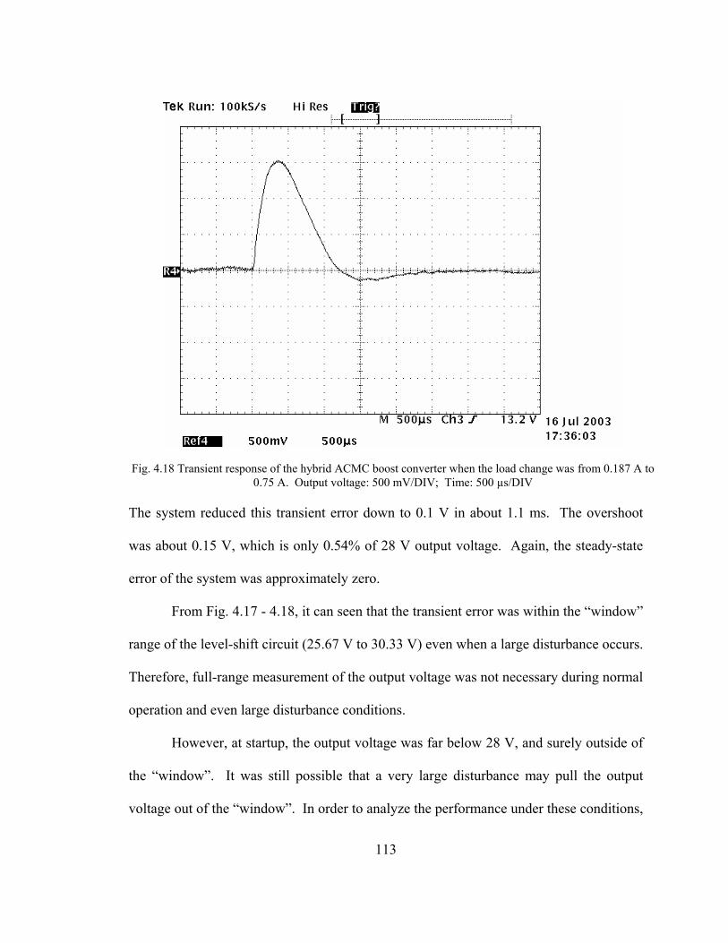
113
The system reduced this transient error down to 0.1 V in about 1.1 ms. The overshoot
was about 0.15 V, which is only 0.54% of 28 V output voltage. Again, the steady-state
error of the system was approximately zero.
From Fig. 4.17 - 4.18, it can seen that the transient error was within the “window”
range of the level-shift circuit (25.67 V to 30.33 V) even when a large disturbance occurs.
Therefore, full-range measurement of the output voltage was not necessary during normal
operation and even large disturbance conditions.
However, at startup, the output voltage was far below 28 V, and surely outside of
the “window”. It was still possible that a very large disturbance may pull the output
voltage out of the “window”. In order to analyze the performance under these conditions,
Fig. 4.18 Transient response of the hybrid ACMC boost converter when the load change was from 0.187 A to 0.75 A. Output voltage: 500 mV/DIV; Time: 500 µs/DIV

114
the step response of the hybrid ACMC system was tested by changing the voltage
reference. Since the voltage loop is a digital controller, the reference change was realized
by setting the voltage reference digitally from 00h to 7Fh and vice versa. This was
equivalent to change the output voltage from 12 V to 28 V and vice versa. The system
was tested under the nominal load condition, that is, the load is 50 Ω. Fig. 4.19 shows the
response when the voltage reference changes from 00h to 7Fh. The output voltage
increased from 12 V to 28 V in 1.8 ms, and reached steady state in about 3 ms with a
small overshoot of about 1V, which is 3.57% of 28 V.
In Fig. 4.20, the voltage reference changed from 7Fh to 00h. The output voltage
decreased from 28 V to 12 V in 2.8 ms. At this time, no overshoot occurred.
The step responses in Fig. 4.19 - 4.20 show that the system can maintain stability
to changes in the voltage reference, and the transient response is smooth. The step
change represented in Fig. 4.19 is equivalent to a start up condition, where the output
voltage change is from 12 V to 28 V. Since the output voltage is far below the nominal
value at the beginning of start up, and is out of the “window” of the level-shift circuit, the
calculated control effort is at its maximum, and the difference between the control effort
and the voltage reference is 7Fh. The step responses prove that the system can start up
safely and can operate properly for a large disturbance. Therefore, there is no need to
measure the full-range of the output voltage for start up if the power stage and the
compensator are designed properly.
The analog controller using the UC3886 is designed to control the same boost
converter. When the load changes from 0.75 A to 0.187 A, the system’s response time

115
Fig. 4.19 Step response of the hybrid ACMC boost converter for voltage reference changing from 00h to 7Fh
when load was 0.56 A. Output voltage: 5 V/DIV; Time: 500 µs/DIV
Fig. 4.20 Step response of the hybrid ACMC boost converter for voltage reference changing from 7Fh to 00h
when load was 0.56 A. Output voltage: 5 V/DIV; Time: 500 µs/DIV
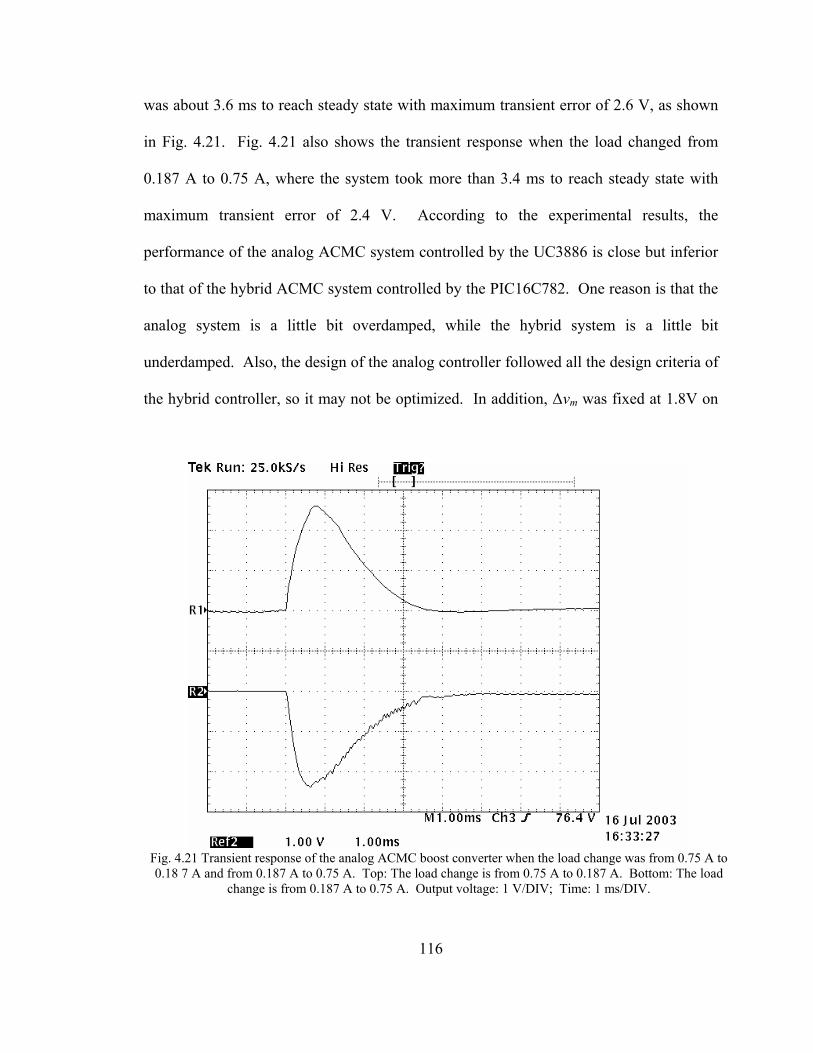
116
was about 3.6 ms to reach steady state with maximum transient error of 2.6 V, as shown
in Fig. 4.21. Fig. 4.21 also shows the transient response when the load changed from
0.187 A to 0.75 A, where the system took more than 3.4 ms to reach steady state with
maximum transient error of 2.4 V. According to the experimental results, the
performance of the analog ACMC system controlled by the UC3886 is close but inferior
to that of the hybrid ACMC system controlled by the PIC16C782. One reason is that the
analog system is a little bit overdamped, while the hybrid system is a little bit
underdamped. Also, the design of the analog controller followed all the design criteria of
the hybrid controller, so it may not be optimized. In addition, Δvm was fixed at 1.8V on
Fig. 4.21 Transient response of the analog ACMC boost converter when the load change was from 0.75 A to 0.18 7 A and from 0.187 A to 0.75 A. Top: The load change is from 0.75 A to 0.187 A. Bottom: The load
change is from 0.187 A to 0.75 A. Output voltage: 1 V/DIV; Time: 1 ms/DIV.

117
the UC3886, which limited the value of Vm and resulted in a smaller overall current loop
gain than the hybrid system. More importantly, there were some differences in the circuit
realization. Because of the previous restrictions, it may be difficult to claim that the
hybrid ACMC system can outperform the analog PCMC system, but it is fair to claim
that the hybrid ACMC system can achieve a performance that is equivalent to the analog
counterpart. In addition, the analog controller is more susceptible to switching noise.
4-5. Conclusion
Presented in this chapter is the practical design of a microcontroller-based average
current mode controller for a boost converter. A PIC16C782 microcontroller, which
provides a one-chip solution, was used to design an ACMC boost converter. The on-
board peripherals of the PIC16C782 are suitable and critical in designing this ACMC
boost converter. Experimental results were also presented, and encouragingly
demonstrate the performance that a microcontroller-based hybrid ACMC converter can
achieve. A pure analog ACMC controller using the UC3886 was designed for
comparison.
Though the microcontroller-based hybrid ACMC has only been applied to a boost
converter, it can be applied to many different converter topologies with minor
modifications.

118
CHAPTER 5
MICROCONTROLLER-BASED FUZZY LOGIC CURRENT-MODE CONTROL
Presented in this chapter is the design and implementation of microcontroller-
based fuzzy logic current-mode control (CMC) for dc-dc converters. Using the
PIC16C782 microcontrollers, a fuzzy logic ACMC controller and a fuzzy logic PCMC
controller have been designed to control a CCM boost converter.
5-1. Fuzzy Logic Control Theory
5-1-1. Introduction of fuzzy logic control in power converter systems
As discussed in previous chapters, CMC power converters are essentially
nonlinear, time-varying systems. The characteristics of these systems impose difficulties
in obtaining accurate mathematical models required for design. Most models used to
design the power converter controllers are linear, small signal models. Usually, there is a
tradeoff between complexity and accuracy for models in the design process. Parasitic
resistances, stray capacitances and leakage inductances increase the difficulty in
obtaining accurate models.
In addition, changes in the operating conditions may result in the change in
system transfer functions. For example, small signal models based on the assumptions
that the signal variation is small, or some parameters, such as input voltage and output
load, are constant. These assumptions may be violated during normal operating
conditions. Also, the changes in ambient conditions, such as temperature, humidity,

119
pressure, etc, may change the electrical characteristics of the circuit components. All
these create difficulties in designing an optimal control system for power converters.
Fuzzy logic control, as a nonlinear control technique, can be a solution to these
difficulties. A fuzzy logic controller is developed based a linguistic description of the
system and not a complicated mathematical model, so it is especially suitable for a
system for which it is difficult to obtain an accurate mathematical model.
Fuzzy logic, first proposed in the 1960’s, is a kind of artificial intelligence that
has been extended to handle the vague concept of partial truth – truth values between
“completely true” and “completely false”. Dr. Lotfi Zadeh, the father of fuzzy logic,
published a serial of papers that introduced fuzzy logic theory in the 1960’s and 1970’s
[57-64]. The fuzzy logic approach provides an effective way of capturing the
approximate, non-exact nature of the way that human beings describe the real world. In
1970’s, fuzzy logic technology began to be applied in control applications. Mamdani and
his colleagues made remarkable contributions to the development of fuzzy logic control
in 1970’s [60-68]. Many other researchers investigated fuzzy logic control intensely [69-
72], and fuzzy logic control has become a new well-known automatic control scheme.
Fuzzy logic controllers have been successfully used in many applications for
many years, such as motor control [80, 85]. Because of the inherent nonlinear and time-
varying nature of switching-mode power converters, fuzzy logic controllers are an
attractive and promising control method for switching-mode power converters.
Therefore, researchers have been investigating the application of fuzzy logic principles to
the control of switching-mode power converters [73-78], including CMC converters [76-
78].

120
Essentially, fuzzy logic control is a digital control method. It can be realized on a
digital signal processor (DSP) [75, 79-80], a field programmable gate arrays (FPGA) [81-
82], a very-large-scale IC (VLSI) [83-84], a microcontroller [85-86], or other types of
digital hardware.
However, the logic and arithmetic calculations of the fuzzy logic algorithm can be
difficult to implement on a low-cost general-purpose microcontroller to control real-time
switch-mode power converter systems. In [87-88], fuzzy logic control has been
successfully applied on a microcontroller to control voltage-mode dc-dc converters. This
provides valuable techniques and considerations in designing fuzzy logic controllers on a
microcontroller.
In order to investigate the feasibility to implement a fuzzy control algorithm for a
real-time CMC dc-dc converter on a low-cost microcontroller, both fuzzy logic ACMC
controller and fuzzy logic PCMC controller have been implemented using a PIC16C782
microcontroller to control dc-dc converters.
5-1-2. Fuzzy sets
In order to clearly understand the fuzzy logic theory, it is necessary to clarify
some of the commonly used terminologies related to fuzzy sets.
Fuzzy set: A set is any collection of objects which can be treated as a whole. To
become a member of a set, certain criteria must be satisfied. To become a member of
fuzzy set, the criterion is not simply “yes” or “no”, “true” or “false”. For example, pick a
set of good students (academically). If a student’s GPA is 4.0, obviously, this student
belongs to the set of good students (a member of the set). If a student has GPA of 2.0, he
is not a member of the set. How about students who have a GPA of 2.8, 3.0 and 3.2?

121
Here, the criterion to become a member of the set is fuzzy (non-discrete, non-distinct,
continuous).
Degree of membership: Degree of membership is used to describe the transition
from membership to non-membership. In the previous example, a student with 3.9 GPA
has higher degree of membership than a student with 3.2 GPA to be in the set of good
students. An object’s grade of membership to a fuzzy set is a real number between 0 and
1, and usually is denoted by the symbol μ. The higher is the number, the higher degree of
membership. Fig. 5.1 shows sets of students and their grades of membership. For a
special case where all elements of a set have full membership, i.e., μ = 1, the set is called
crisp (non-fuzzy, discrete) set.
Universe of discourse: Universe of discourse is the collection of all elements that
can come into consideration for a fuzzy set. For example, referring to Fig. 5.1, the fuzzy
set of good students is taken from students as a universe of discourse. Every element in
the universe of discourse is a member of the fuzzy set to some degree. A very poor
student is a member of the set of very good students with μ = 0.
μ
GPA1.0 2.0 3.0 4.0
1.0
0.5
0
Poor students
Ordinary students
Good students
Very poor students Very good students
Fig. 5.1 The sets very poor students, poor student, ordinary students, good students and very good students are derived from students as a universe of discourse.

122
Membership function: Since every member of a fuzzy set has a degree of
membership associated with it, a fuzzy set can be viewed as a set of ordered pairs of
generic elements and their degrees of membership. Every element of the universe of
discourse has exactly one μ to a fuzzy set. That is, each element of the universe of
discourse is represented by exactly one ordered pair. This defines a mapping between
elements of the universe discourse and the degrees of membership to the fuzzy set, and
this mapping is defined to be the membership function μ(x) of the fuzzy set. In practice,
the terms “membership function” and “fuzzy set” are usually interchangeable.
Support, crossover point and fuzzy singleton: The crisp set of all elements that
have a non-zero membership (μ ≠ 0) is called the support of the fuzzy set. In particular,
the element with μ = 0.5 is called the crossover point. If a fuzzy set whose support is a
single point with μ = 1.0, then this fuzzy set is a fuzzy singleton.
The operations on fuzzy sets by means of their membership functions create new
fuzzy sets from given fuzzy sets. There are totally three basic fuzzy set operations: union,
intersection and complement. Let fuzzy sets A and B belongs to a universe discourse U
with μA(x) and μB(x) as their membership functions, respectively.
The union of A and B is denoted by A∪B, and the membership function of A∪B is
defined by:
μA∪B(x) = maxμA(x), μB(x). (5-1)
The intersection of A and B is denoted by A∩B, and the membership function of
A∩B is defined by:
μA∩B(x) = minμA(x), μB(x). (5-2)
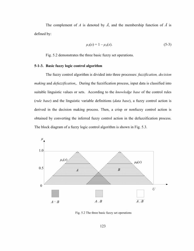
123
The complement of A is denoted by Ā, and the membership function of Ā is
defined by:
μĀ(x) = 1 – μA(x). (5-3)
Fig. 5.2 demonstrates the three basic fuzzy set operations.
5-1-3. Basic fuzzy logic control algorithm
The fuzzy control algorithm is divided into three processes: fuzzification, decision
making and defuzzification,. During the fuzzification process, input data is classified into
suitable linguistic values or sets. According to the knowledge base of the control rules
(rule base) and the linguistic variable definitions (data base), a fuzzy control action is
derived in the decision making process. Then, a crisp or nonfuzzy control action is
obtained by converting the inferred fuzzy control action in the defuzzification process.
The block diagram of a fuzzy logic control algorithm is shown in Fig. 5.3.
µ
U
1.0
0.5
0
A B
A B
A B A B
µA(x) µB(x)
Fig. 5.2 The three basic fuzzy set operations
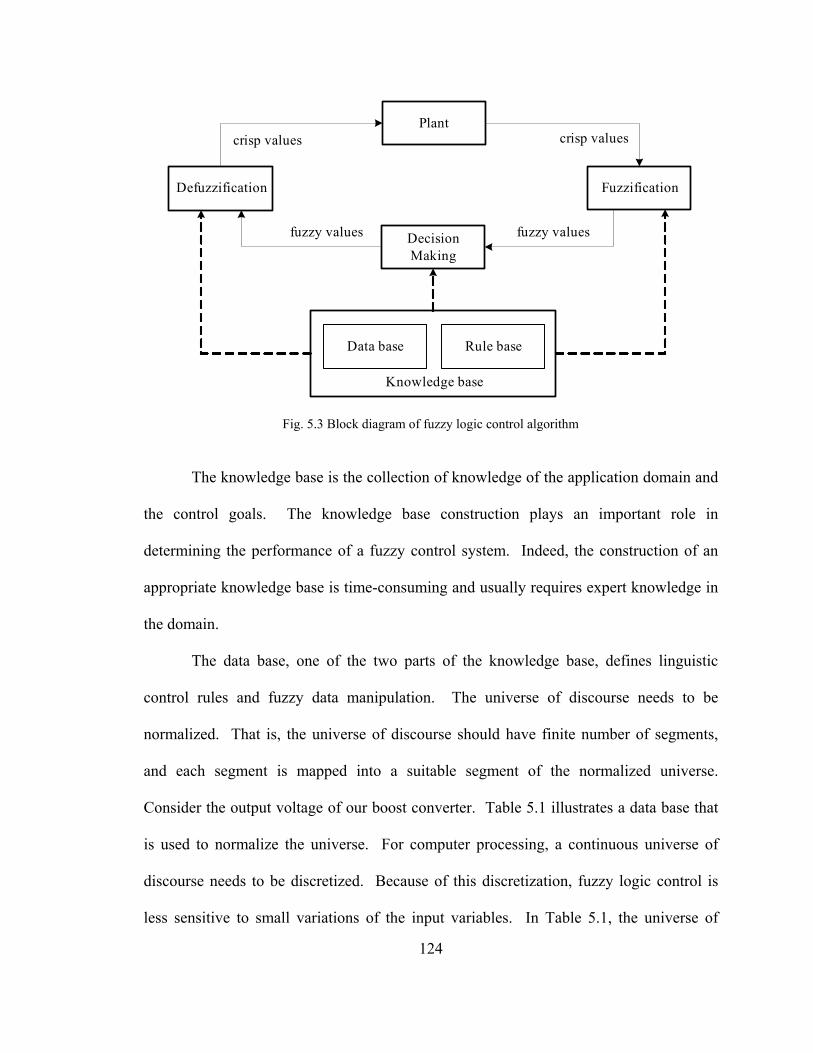
124
The knowledge base is the collection of knowledge of the application domain and
the control goals. The knowledge base construction plays an important role in
determining the performance of a fuzzy control system. Indeed, the construction of an
appropriate knowledge base is time-consuming and usually requires expert knowledge in
the domain.
The data base, one of the two parts of the knowledge base, defines linguistic
control rules and fuzzy data manipulation. The universe of discourse needs to be
normalized. That is, the universe of discourse should have finite number of segments,
and each segment is mapped into a suitable segment of the normalized universe.
Consider the output voltage of our boost converter. Table 5.1 illustrates a data base that
is used to normalize the universe. For computer processing, a continuous universe of
discourse needs to be discretized. Because of this discretization, fuzzy logic control is
less sensitive to small variations of the input variables. In Table 5.1, the universe of
Defuzzification
Decision Making
Fuzzification
Plantcrisp values
fuzzy values fuzzy values
crisp values
Data base Rule base
Knowledge base
Fig. 5.3 Block diagram of fuzzy logic control algorithm
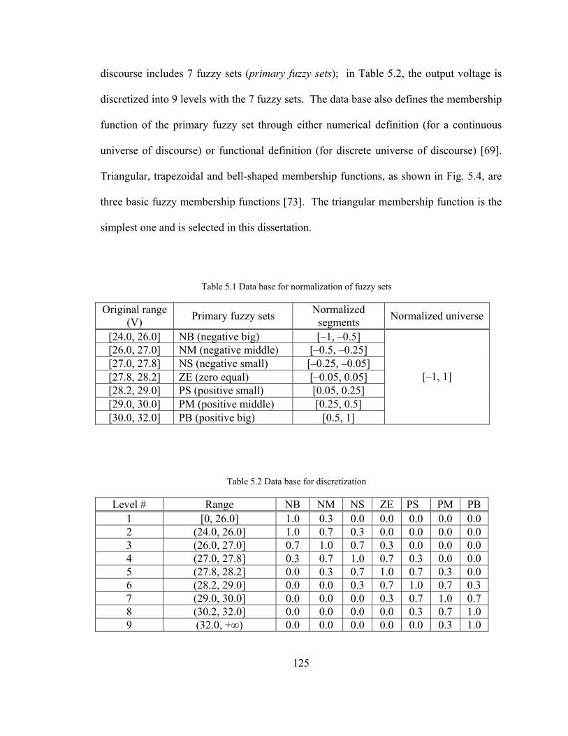
125
discourse includes 7 fuzzy sets (primary fuzzy sets); in Table 5.2, the output voltage is
discretized into 9 levels with the 7 fuzzy sets. The data base also defines the membership
function of the primary fuzzy set through either numerical definition (for a continuous
universe of discourse) or functional definition (for discrete universe of discourse) [69].
Triangular, trapezoidal and bell-shaped membership functions, as shown in Fig. 5.4, are
three basic fuzzy membership functions [73]. The triangular membership function is the
simplest one and is selected in this dissertation.
Table 5.1 Data base for normalization of fuzzy sets
Original range (V) Primary fuzzy sets Normalized
segments Normalized universe
[24.0, 26.0] NB (negative big) [–1, –0.5] [26.0, 27.0] NM (negative middle) [–0.5, –0.25] [27.0, 27.8] NS (negative small) [–0.25, –0.05] [27.8, 28.2] ZE (zero equal) [–0.05, 0.05] [28.2, 29.0] PS (positive small) [0.05, 0.25] [29.0, 30.0] PM (positive middle) [0.25, 0.5] [30.0, 32.0] PB (positive big) [0.5, 1]
[–1, 1]
Table 5.2 Data base for discretization
Level # Range NB NM NS ZE PS PM PB1 [0, 26.0] 1.0 0.3 0.0 0.0 0.0 0.0 0.02 (24.0, 26.0] 1.0 0.7 0.3 0.0 0.0 0.0 0.03 (26.0, 27.0] 0.7 1.0 0.7 0.3 0.0 0.0 0.04 (27.0, 27.8] 0.3 0.7 1.0 0.7 0.3 0.0 0.05 (27.8, 28.2] 0.0 0.3 0.7 1.0 0.7 0.3 0.06 (28.2, 29.0] 0.0 0.0 0.3 0.7 1.0 0.7 0.37 (29.0, 30.0] 0.0 0.0 0.0 0.3 0.7 1.0 0.78 (30.2, 32.0] 0.0 0.0 0.0 0.0 0.3 0.7 1.09 (32.0, +∞) 0.0 0.0 0.0 0.0 0.0 0.3 1.0
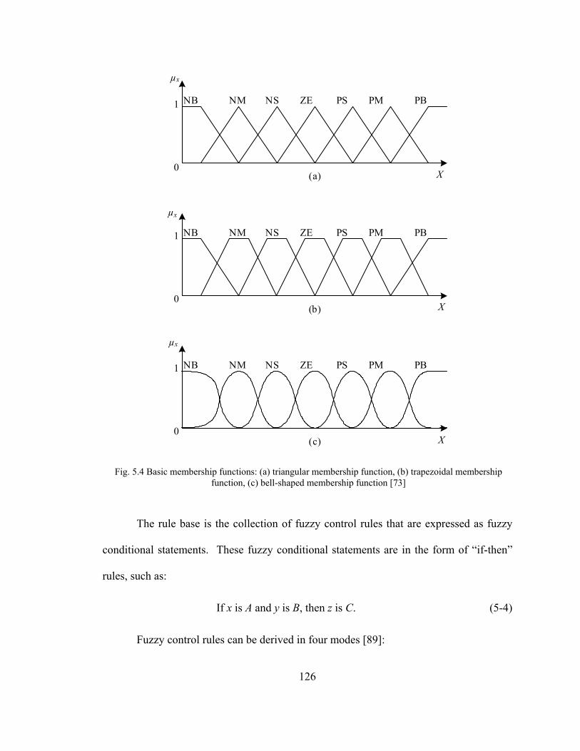
126
The rule base is the collection of fuzzy control rules that are expressed as fuzzy
conditional statements. These fuzzy conditional statements are in the form of “if-then”
rules, such as:
If x is A and y is B, then z is C. (5-4)
Fuzzy control rules can be derived in four modes [89]:
1
0
NB NM NS ZE PS PM PB
µx
(a) X
1
0
NB NM NS ZE PS PM PB
µx
(b) X
1
0
NB NM NS ZE PS PM PB
µx
(c) X
Fig. 5.4 Basic membership functions: (a) triangular membership function, (b) trapezoidal membership function, (c) bell-shaped membership function [73]

127
― Expert experience and control engineering knowledge;
― Operator’s control action;
― Fuzzy model of a process;
― Learning.
The fuzzification process is a methodology to generalize a specific element from a
crisp value to a fuzzy value. During this process, input variables are measured and are
mapped into corresponding universes of discourse by converting the input data into
suitable linguistic values which may be viewed as labels of fuzzy sets. The fuzzification
process is guided by the data base.
In the decision-making process, a fuzzy control action is derived in the framework
of fuzzy logic and approximate reasoning following the fuzzy control rules. Those fuzzy
control rules are expressed as fuzzy implications. The definition of a fuzzy implication
can be expressed as a fuzzy implication function. Researchers have proposed dozens of
implication functions, such as Mamdani’s mini-operation rule of fuzzy implication and
Larsen’s product operation rule of fuzzy implication. They are the mostly commonly
used inference mechanism of the fuzzy reasoning [70, 74, 90]. If the fuzzy variables are
fuzzy singletons, the two fuzzy reasoning approaches yield the same results, and can be
expressed as:
zi = minμAi(x0),…, μBi(y0)•Ci, (5-5)
where x0 and y0 are fuzzy singletons, Ai, Bi and Ci are fuzzy sets in universes X, Y and Z,
and Ci is the singleton value of z using the ith rule. The graphical representation of this
method is illustrated in Fig. 5.5. This fuzzy implication method will be used in this
dissertation to design the fuzzy logic CMC controllers.

128
Defuzzification maps fuzzy control action to crisp (nonfuzzy) control action. This
operation is required because most practical applications use crisp control action. In the
decision-making operation, many control actions are usually derived. The defuzzification
process combines those fuzzy control actions through defuzzification strategies.
Commonly used strategies include the maximum criterion method, the mean of maximum
method, and the center of gravity method [70].
The maximum criterion method: This method finds the point where its
membership function is the maximum, which can be expressed as:
)(max)(0 iziz wwwz μμ == , (5-6)
where z0 is the crisp control action, and wi is the support value at which the membership
function reaches the maximum.
The mean of maximum method: This method averages all the control actions
for which their membership functions are a maximum. This method can be expressed as:
1.0
0X
A1
µA1
Y
µB1
B1
1.0
0X
A2
µA2
Y
µB2
B2
Z
µC1
C1
Z
µC2
C2
x0 y0
Z
µC
Fig. 5.5 Graphic representation of fuzzy reasoning [70]
129
∑=
=n
i
i
nwz
10 , (5-7)
where n is number of local crisp control actions. This method is used in this dissertation
to obtain the crisp control action to control the fuzzy logic ACMC boost converter.
The center of gravity method: This method is the most widely used. This
method finds the center of gravity of all the local control actions. The final crisp control
action can be found by:
∑
∑ ⋅= n
iiz
n
iiiz
w
wwz
)(
)(0
μ
μ. (5-8)
This method is used in this dissertation to obtain the crisp control action to control
the fuzzy logic PCMC boost converter.
5-2. Microcontroller-Based Fuzzy Logic ACMC Power Converters
This section describes the design and implementation considerations for
microcontroller-based fuzzy logic ACMC converters. Using the PIC16C782, a hybrid
fuzzy logic ACMC controller has been designed to control the same boost converter
described in Chapter 4. A one-chip solution has been achieved, and encouragingly
demonstrates that the fuzzy logic current-mode control of DC-DC converters can be
implemented using a microcontroller.
5-2-1. System overview
The block diagram for the microcontroller-based fuzzy logic ACMC boost
converter is shown in Fig. 5.6. In the current loop, a current amplifier, which is
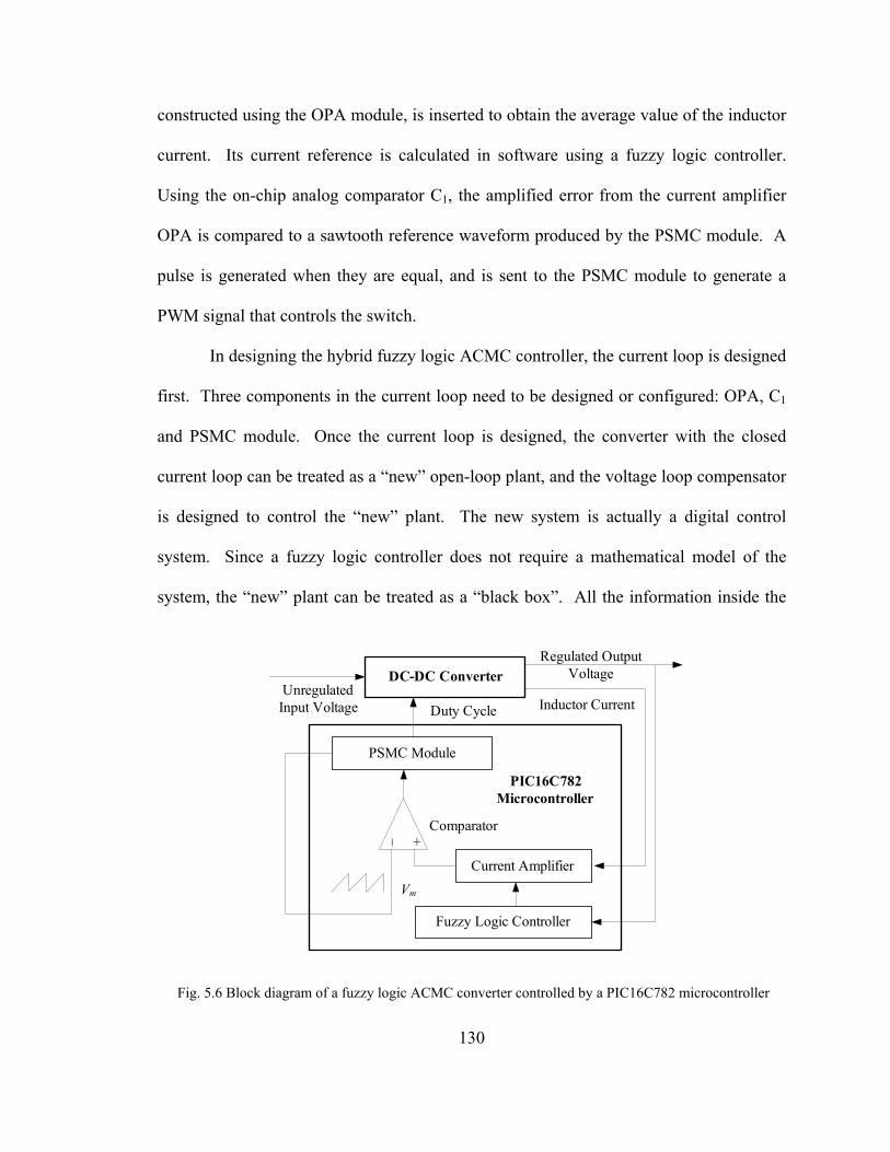
130
constructed using the OPA module, is inserted to obtain the average value of the inductor
current. Its current reference is calculated in software using a fuzzy logic controller.
Using the on-chip analog comparator C1, the amplified error from the current amplifier
OPA is compared to a sawtooth reference waveform produced by the PSMC module. A
pulse is generated when they are equal, and is sent to the PSMC module to generate a
PWM signal that controls the switch.
In designing the hybrid fuzzy logic ACMC controller, the current loop is designed
first. Three components in the current loop need to be designed or configured: OPA, C1
and PSMC module. Once the current loop is designed, the converter with the closed
current loop can be treated as a “new” open-loop plant, and the voltage loop compensator
is designed to control the “new” plant. The new system is actually a digital control
system. Since a fuzzy logic controller does not require a mathematical model of the
system, the “new” plant can be treated as a “black box”. All the information inside the
DC-DC Converter
Fuzzy Logic Controller
+ _
Vm
Comparator
PSMC Module
Unregulated Input Voltage
Regulated Output Voltage
Inductor CurrentDuty Cycle
PIC16C782Microcontroller
Current Amplifier
Fig. 5.6 Block diagram of a fuzzy logic ACMC converter controlled by a PIC16C782 microcontroller

131
“box” is not required. Since the control action in a fuzzy logic controller is determined
from the evaluation of a set of linguistic rules, more than one type of DC-DC converter
could share the same control scheme without any modification.
Since the circuit and design method of the current loop are identical to the hybrid
ACMC system described in Chapter 4, they will not be discussed in this section.
5-2-2. Fuzzy logic controller
The fuzzy logic controller inside the PIC16C782 is shown in Fig. 5.7. The inputs
of the fuzzy logic controller are the error e and the change of error ce of the output
voltage of the boost converter. The sampled output voltage is used to create these two
inputs. The error e can be expressed as
Fuzzification
ADCPIC16C782
Microcontroller
Vref
vo
Decision Making
e(k-1)+
+
–
–
Defuzzification
DAC
e(k)z-1
ce(k)
z-1
vc(k)
vc(k) +
+vc(k-1)
vc
δ vc(k)
vo(k)
Fig. 5.7 Fuzzy logic controller inside the PIC16C782 microcontroller for ACMC boost converter
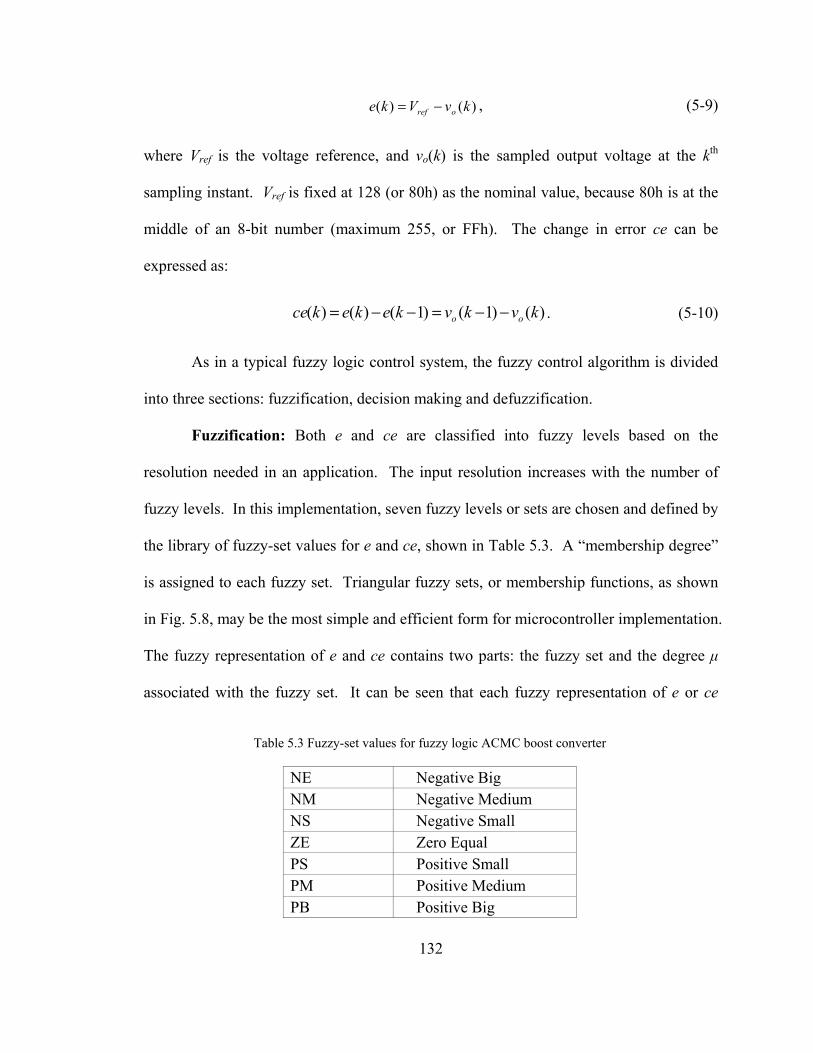
132
)()( kvVke oref −= , (5-9)
where Vref is the voltage reference, and vo(k) is the sampled output voltage at the kth
sampling instant. Vref is fixed at 128 (or 80h) as the nominal value, because 80h is at the
middle of an 8-bit number (maximum 255, or FFh). The change in error ce can be
expressed as:
)()1()1()()( kvkvkekekce oo −−=−−= . (5-10)
As in a typical fuzzy logic control system, the fuzzy control algorithm is divided
into three sections: fuzzification, decision making and defuzzification.
Fuzzification: Both e and ce are classified into fuzzy levels based on the
resolution needed in an application. The input resolution increases with the number of
fuzzy levels. In this implementation, seven fuzzy levels or sets are chosen and defined by
the library of fuzzy-set values for e and ce, shown in Table 5.3. A “membership degree”
is assigned to each fuzzy set. Triangular fuzzy sets, or membership functions, as shown
in Fig. 5.8, may be the most simple and efficient form for microcontroller implementation.
The fuzzy representation of e and ce contains two parts: the fuzzy set and the degree μ
associated with the fuzzy set. It can be seen that each fuzzy representation of e or ce
Table 5.3 Fuzzy-set values for fuzzy logic ACMC boost converter
NE Negative Big NM Negative Medium NS Negative Small ZE Zero Equal PS Positive Small PM Positive Medium PB Positive Big

133
belongs to at most two fuzzy sets. For example, when e equals -0.625, its fuzzy sets are
NB and NM with degrees of 5.0)()( == ee NMNB μμ .
Decision-making: General knowledge of the converter behavior and design
experiences are the basis to derive the control rules that associate the fuzzy input and
fuzzy output. The rule base used in this implementation including following criteria [74]:
1) When the output of the converter is far from the set point, the change of duty
cycle must be large so as to bring the output to the set point quickly;
2) When the output of the converter is approaching the set point, a small change
of duty cycle is necessary;
3) When the output of the converter is near the set point and is approaching it
rapidly, the duty cycle must be kept constant so as to prevent overshoot;
4) When the set point is reached and the output is still changing, the duty cycle
must be changed a little bit to prevent the output from moving away;
5) When the set point is reached and the output is steady, the duty cycle remains
unchanged;
6) When the output is above the set point, the sign of the change of duty cycle
-1.0 -0.75 -0.5 -0.25 0 0 .25 0 .5 0 .75 1 .0
1
0
NB NM NS ZE PS PM PB
µ(e), µ(ce)
Fig. 5.8 Membership functions for e and ce

134
must be negative, and vice versa;
Table 5.4 is the rule table derived from the above fuzzy control rules. However,
the control rules are usually developed using “trial and error” and from an “intuitive” feel
of the process being controlled. Since every e and ce belongs to at most two fuzzy sets,
any combination of feedback samples of signals (e, ce) can result in a maximum of four
control rules. The inference result of each rule consists of two parts: change in control
effort Ci and its weighting factor wi. Change in control effort Ci is obtained directly from
the control rule table (Table 5.4). The inferred output of each rule is written as:
iiiiii CwCceez == )(),(min μμ , (5-11)
where zi is the fuzzy representation output of change in control effort inferred by the ith
control rule. Since zi is a linguistic result, a defuzzification operation is required next to
obtain a crisp result.
Defuzzification: The most desirable way to perform the defuzzification operation
is the center of gravity method, where the crisp value of change in control effort δvc can
be computed by a logical sum of the inference results of the four control rules:
Table 5.4 Control rule table for fuzzy logic ACMC boost converter
Error NB NM NS ZE PS PM PB
NB NB NB NB NB NM NS ZE NM NB NB NB NM NS ZE PS NS NB NB NM NS ZE PS PM ZE ZB NM NS ZE PS PM PB PS NM NS ZE PS PM PB PB PM NS ZE PS PM PB PB PB C
hang
e in
Err
or
PB ZE PS PM PB PB PB PB
135
∑
∑
=
== 4
1
4
1
ii
iii
c
w
mwvδ , (5-12)
where mi is the centroid of Ci. Notice that (5-12) involves multiplication and division of
variables, not just the scaling of signals by constant gains. Many microcontrollers, just as
the PIC16C782, do not have direct multiplication and division instructions, so they do not
have the capacity to compute the control effort fast enough to control the converter
satisfactorily. In order to solve this problem, Gupta et al. [87] developed a modified
centroid method, which can be expressed as:
2
bac
mmv +=δ , (5-13)
where ma and mb are the centroids corresponding to the two largest degrees of the fuzzy
sets belonging to the fuzzy representation of the change in control effort. The modified
centroid method requires only one addition and a right-shift. However, this method is
valid only if the centroids of adjacent fuzzy sets are close to each other, and does not give
comparable results if the centroids are far apart. Also, this method needs to search out
the two largest degrees, which slows down the computation significantly, since many
microcontrollers, including the PIC16C782, do not have direct instructions for
comparison.
The mean of maximum method is another defuzzification strategy. This strategy
yields a control action that represents the mean value of all control rules whose
membership functions reach the maximum. In this implementation, the control action can
be expressed as:

136
∑=
=4
141
iic mvδ , (5-14)
where mi is the centroid corresponding to each of the four largest degrees of the fuzzy
sets belonging to the fuzzy representation of the change in control effort.
Equation (5-14) shows that δvc is simply the average of the centroids of all the
four fuzzy representations of the change in control effort. When using this method, the
action of the fuzzy logic controller is similar to that of a multilevel relay system. This
method is actually a special case of the center of gravity method when wi = 1 for all i.
The mean of maximum method yields a better transient performance, while the center of
gravity method yields a better steady-state performance [70].
The output of the fuzzy control algorithm is the change in control effort δvc(k).
The actual control effort vc(k) is determined by adding the previous control effort vc(k-1)
to the calculated change in control effort δvc(k), which can expressed as
vc(k) = vc(k – 1) + δvc(k). (5-15)
In classical control theory, (5-15) represents an integrating process which
increases the system type and reduces the steady-state error. The calculated control effort
vc(k) is then sent to the current compensator as the current reference.
5-2-3. Implementation challenges and solutions
In Chapter 2-4, the solutions that solve the challenges facing to hybrid CMC
power converter have been presented. Most of the solutions can also be applied to hybrid
fuzzy logic ACMC system. In this implementation, some of challenges are solved using
different approaches. In addition, there are some new challenges that need to be solved.

137
The PIC16C782 does not allow negative numbers in the system. However, e and
ce can have negative physical values. Therefore, their digital representations e and ec ˆ
are biased by 128:
⎪⎩
⎪⎨
⎧
≤<=
<≤
⎪⎩
⎪⎨
⎧
>=<
255ˆ,ˆ128128ˆ,ˆ
128ˆ,ˆ0then,
000
,ece
eceece
cee . (5-16)
where the variables e and ec ˆ are the error and change in error with the 128 offset,
respectively. When an overflow or an underflow occurs, 255 or 0 is set for a maximum
or minimum value. As the result, the universe of discourse for the membership functions
for e and ec ˆ extends from 0 to 255, and is spaced equally. The resultant δvc is also
biased by 128, and needs to be adjusted back before it is added to vc.
In order to achieve simple and fast computation, the mean of maximum method is
employed in the defuzzification process. This method requires only three additions and
three right-shifts without any other calculations, and hence reduces the computation
complexity dramatically. By using the carry as an extra bit during addition and followed
by right-shift through carry, the calculation procedure becomes 9 bits instead of 8.
Therefore, the calculation procedure is guaranteed to not overflow, which further
simplifies the calculation procedure without sacrificing any accuracy.
When the mean of maximum method is used, only the centroids of the fuzzy sets
are required in the calculation. Therefore, the degrees associated with the fuzzy sets are
not calculated or stored. This further simplifies the calculation procedure and saves
memory space.
The control rules (Table 5.4) are stored as a look-up table that contains the

138
centroids of the output fuzzy sets. The output fuzzy sets for change in control effort δvc
follow the universe of discourse as shown in Fig. 5.9. Note δvc in Fig. 5.9 has an offset
of 128. The range for the universe of discourse is limited because only seven output
fuzzy sets are chosen. This limits the maximum δvc, and hence limits the maximum
change in duty cycle δd. Extensive experimental tests show that the overshoot in the
transient response can be very large if δd is too large, which may result in instability.
As stated previously, the mean of maximum method has a relatively poor steady-
state performance because of its relay-like characteristic, which results in a steady-state
error and a triangular ripple in the output voltage. Therefore, the range for the universe
of discourse should be small enough such that the change in control effort is small
enough to eliminate the steady-state ripple and error. That is, the centroids of adjacent
output fuzzy sets are close to each other. Since the change in control effort δvc is very
small at steady state, it is especially important to have closer fuzzy sets when δvc is small,
which is also shown in Fig. 5.9.
On the other hand, a smaller range of change in control effort results in smaller
change in control effort, which slows down the transient response. Therefore, there is a
tradeoff between transient and steady-state performances. This tradeoff can be
0 74 102 122 128 134 154 182 255
255NB NM NS ZE PS PM PB
µ(dvc)
Fig. 5.9 Membership function (1) for δvc
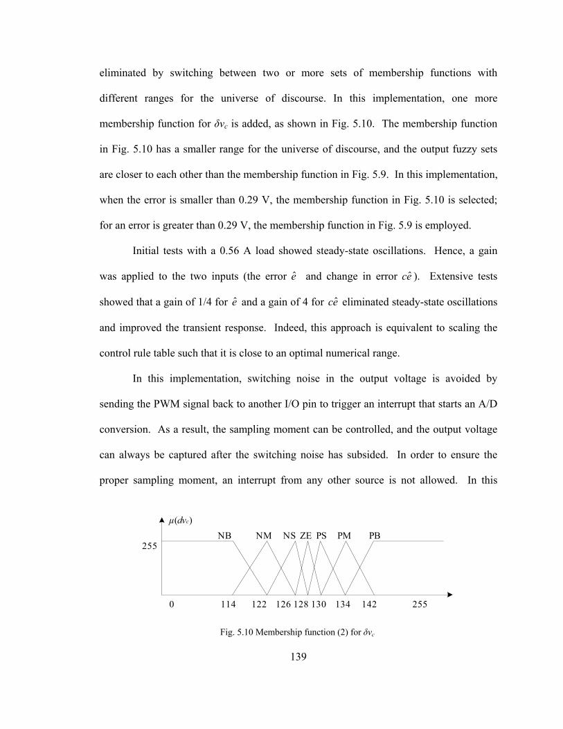
139
eliminated by switching between two or more sets of membership functions with
different ranges for the universe of discourse. In this implementation, one more
membership function for δvc is added, as shown in Fig. 5.10. The membership function
in Fig. 5.10 has a smaller range for the universe of discourse, and the output fuzzy sets
are closer to each other than the membership function in Fig. 5.9. In this implementation,
when the error is smaller than 0.29 V, the membership function in Fig. 5.10 is selected;
for an error is greater than 0.29 V, the membership function in Fig. 5.9 is employed.
Initial tests with a 0.56 A load showed steady-state oscillations. Hence, a gain
was applied to the two inputs (the error e and change in error ec ˆ ). Extensive tests
showed that a gain of 1/4 for e and a gain of 4 for ec ˆ eliminated steady-state oscillations
and improved the transient response. Indeed, this approach is equivalent to scaling the
control rule table such that it is close to an optimal numerical range.
In this implementation, switching noise in the output voltage is avoided by
sending the PWM signal back to another I/O pin to trigger an interrupt that starts an A/D
conversion. As a result, the sampling moment can be controlled, and the output voltage
can always be captured after the switching noise has subsided. In order to ensure the
proper sampling moment, an interrupt from any other source is not allowed. In this
0 114 122 126 128 130 134 142 255
255NB NM NS ZE PS PM PB
µ(dvc)
Fig. 5.10 Membership function (2) for δvc

140
implementation, the interrupt service routine (ISR) also contains all logical and
mathematical calculations, and the main routine simply waits for the next interrupt after
all the calculations have been finished. Since the A/D conversion time is much faster
than total calculation time, the controller sampling frequency is directly determined by
the speed of the calculations.
5-2-4. Experimental results
The system diagram for the microcontroller-based fuzzy logic ACMC boost
converter is shown in Fig. 5.11. The power stage is the same boost converter described
in Chapter 4. The nominal input and output voltages of the boost converter were 12 V
and 28 V, respectively, and the nominal load was 50 Ω (0.56 A). AC coupling was
utilized on the oscilloscope channel in measuring the output voltage. The boost converter
PIC16C782
ADC
Fuzzy Logic Controller
A
PSMC
SC
DAC
+ _
12 V5 V
5 VRB6/C1/PSMC1A
RB7/C2/PSMC1B
RB0/INT
C1RB2/AN6
RA2/AN2
VDD
AVDD
_____RA5/MCLR/VPP
RB4Check Calculation Timing
RB1/VDAC
RA7/OSC1
RA6/OSC2Vss
AVss
20
7
19
14
13
916
15
4
11
10
18
17
5
6
Interrupt(Start ADC)
Gate Drive
Load
R1
C1
Boost Converter
R2
+ _
RA0/OPA+
RB3/OPA
RA1/OPA–1
2OPA
Cfp
CfzRf
Rl
Ri
RC
L
RA3/AN3/VREF18
+ _
5 V
+ _
R3
R4
Fig. 5.11 A fuzzy logic ACMC boost converter controlled by a PIC16C782

141
operated in CCM when the switching frequency was 156.25 kHz, or 6.4 μs per switching
cycle. The PIC16C782 operated at 20 MHz. All waveforms were recorded using a
Tektronix TDS 744A oscilloscope.
Fig. 5.12 shows the calculation timing status. The top line is the gate signal. The
bottom line is obtained by toggling an output pin when the program enters or exits the
ISR, so it represents the time required to finish all arithmetic and logic calculations. Fig.
5.12 shows that all calculations can be completed in around 31 μs, so the output voltage
can be sampled every 5 switching cycles, or 32 μs. This is much longer than the ADC
conversion cycle, which is only 15.2 μs when the clock frequency is 20 MHz. Fig. 5.13
is the same as Fig. 5.12, except it has an expanded time axis. Fig. 5.13 clearly shows that
Fig. 5.12 Gate and ISR timing diagram 1. Top: gate signal, 10 V/DIV; Bottom: timing signal on an output
pin, 2 V/DIV; Time: 5 μs/DIV

142
A/D conversion is started 1.2 μs after the switch is turned on, when the switching noise
has subsided. The starting point of each A/D conversion can be controlled precisely at a
0.2 μs (one instruction cycle) precision.
When a large disturbance occurs, such as a load change from 0.187 A to 0.75 A ,
as shown in Fig. 5.14, the response time of the system was around 1 ms to reach steady
state with 1.2 V (4.3% of 28 V) of maximum transient error. At this time, the transient
error was reduced to less than 0.3 V (1% of 28 V) in 300 μs. When the load change was
from 0.75 A to 0.187 A, as shown in Fig. 5.15, the system required 1.5 ms to reach steady
state with 1.3 V (4.6% of 28 V) of maximum transient error. At this time, the transient
error was reduced to 0.3 V in less than 600 μs. In both cases, the steady-state error of the
system was approximately zero. The top lines in Fig. 5.14 and Fig. 5.15 are the full range
Fig. 5.13 Gate and ISR timing diagram 2. Top: gate signal, 10 V/DIV; Bottom: timing signal on an output pin, 2 V/DIV; Time: 1 μs/DIV

143
Fig. 5.14 Transient response of the fuzzy logic ACMC boost converter when the load change was from 0.187
A to 0.75 A. Top: output voltage, 10 V/DIV; Bottom: output voltage, 500 mV/DIV; Time: 500 μs/DIV
Fig. 5.15 Transient response of the fuzzy logic ACMC boost converter when the load change was from 0.75 A to 0.187 A. Top: output voltage, 10 V/DIV; Bottom: output voltage, 500 mV/DIV; Time: 500 μs/DIV

144
of the output voltage, and the bottom lines are the AC coupled output voltage.
The step response for the voltage reference, illustrated in Fig. 5.16, was obtained
by changing Vref from 00h to 80h (nominal value). The step response shows that the
system reaches steady state in less than 2 ms with an overshoot of about 1.5 V, which is
about 5.4% of 28 V. This proves that there is no need to measure the full-range of the
output voltage for start up if the voltage loop compensator is designed appropriately.
5-3. Microcontroller-Based Fuzzy Logic PCMC Power Converters
Described in this section are the design and implementation considerations for a
microcontroller-based fuzzy logic PCMC converter. A hybrid fuzzy logic PCMC boost
converter has been implemented using a PIC16C782 microcontroller. For generality, the
Fig. 5.16 Step response of the fuzzy logic ACMC boost converter. Output voltage: 5 V/DIV; Time: 500
μs/DIV

145
boost converter operates in the continuous conduction mode (CCM). By using the on-
board peripherals of the microcontroller and rule-based look-up tables, a one-chip
solution has been achieved. Experimental results indicate successful operation of the
fuzzy logic implementation for a PCMC dc-dc converter.
5-3-1. System overview
The block diagram for the microcontroller-based fuzzy logic PCMC boost
converter is shown in Fig. 5.17. In the current loop, the peak switch current (inductor
current) is sensed by a low-value resistor Ri. The on-board comparator C1 compares the
peak switch current (after slope compensation) with a reference current, which is
calculated in software using fuzzy logic. A pulse is generated when they are equal, and is
sent to the PSMC module to generate a PWM signal that controls the switch. The PSMC
module is also used to generate a positive-going ramp function to perform slope
DC-DC Converter
Fuzzy Logic Controller
Comparator
PSMC Module
Unregulated Input Voltage
Regulated Output Voltage
Inductor CurrentDuty Cycle
PIC16C782Microcontroller+ _
Slope Compensation
+
+
Fig. 5.17 Block diagram of a fuzzy logic PCMC converter controlled by a PIC16C782 microcontroller

146
compensation by adding it to the sensed current. Design procedures are the same as
hybrid fuzzy logic ACMC power converter described in previous section.
Since the current loop design is identical to the hybrid PCMC power converter
introduced in Chapter 3, it will not be discussed in this section.
5-3-2. Fuzzy logic controller
Once the current loop is designed, the converter with the closed current loop can
be treated as a “new” open loop plant, and the voltage loop compensator is designed to
control the “new” plant. Since a fuzzy logic controller does not need a converter model,
the “new” plant can be treated as a “black box”. Only knowledge of the converter
behavior, in the form of linguistic rules, is needed. The fuzzy control algorithm is
divided into three sections: fuzzification, decision making and defuzzification. The
output of the fuzzy control algorithm is the change in control effort δvc(k).
Fuzzification: Just as the hybrid fuzzy logic ACMC system, the inputs of the
fuzzy controller are the error e, the change of error ce. Since e and ce can have negative
physical values, their digital representations are biased by 128.
Both e and ce are classified into fuzzy levels based on the resolution needed in an
application. The input resolution increases with the number of fuzzy levels. In this
implementation, nine fuzzy levels or sets are chosen and defined by the library of fuzzy-
set values for e and ce, as shown in Table 5.5. A “membership degree” can be assigned
to each fuzzy set. Triangular fuzzy-sets, or membership functions, as shown in Fig. 5.18,
were selected here, since it is the simplest and most efficient form for microcontroller
implementation. The fuzzy representation of e and ce contains two parts: the fuzzy set
and the degree μ associated with the fuzzy set. It can be seen that each fuzzy

147
representation of e or ce belongs to at most two fuzzy sets. For example, when the digital
representation of e equals 24, its fuzzy sets are NB and NM with degrees of
192)( =eNBμ and 64)( =eNMμ .
Decision-making: General knowledge of the converter behavior is the basis on
which to derive control rules that associate the fuzzy input and fuzzy output. Table 5.6
contains the control rules to determine the fuzzy set output. Since every e and ce belongs
to at most two fuzzy sets, any combination of feedback samples of signals (e, ce) can
result in a maximum of four control rules. However, the control rules are usually
0 16 32 48 64 80 96 112 128 144 160 176 192 208 224 240 255
µ(e), µ(ce)
NB NM NS NE ZE PE PS PM PB255
Fig. 5.18 Membership functions for e and ce
Table 5.5 Fuzzy-set values for fuzzy logic PCMC boost converter
NB Negative Big NM Negative Medium NS Negative Small NE Negative Equal ZE Zero Equal PE Positive Equal PS Positive Small PM Positive Medium PB Positive Big

148
developed using “trial and error” and from an “intuitive” feel of the process being
controlled. Table 5.6 is obtained by understanding the behavior of the converter. The
inference result of each rule consists of two parts: the degree of change in control effort
Ci, and its weighting factor wi. Ci is obtained directly from Table 5.6, and wi can be
obtained by means of Mamdani’s min fuzzy implication. The inferred output of each rule
can be computed using (5-11).
Defuzzification: The output fuzzy sets for change in control effort δvc follow the
universe of discourse as shown in Fig. 5.19. Note δvc in Fig. 5.19 also has an offset of
128.
As described in previous section, the mean of maximum method yields a control
action that represents the mean value of all control rules whose membership functions
reach the maximum. When using this method, the action of the fuzzy logic controller is
similar to that of a multilevel relay system. This method can be implemented by using
only several additions and right-shifts without any other calculations, and hence reduces
Table 5.6 Control rule table for fuzzy logic PCMC boost converter
Error NB NM NS NE ZE PE PS PM PB
NB NB NB NB NB NB NM NS NE ZE NM NB NB NB NB NM NS NE ZE PE NS NB NB NB NM NS NE ZE PE PS NE NB NB NM NS NE ZE PE PS PM ZE NB NM NS NE ZE PE PS PM PB PE NM NS NE ZE PE PS PM PB PB PS NS NE ZE PE PS PM PB PB PB PM NE ZE PE PS PM PB PB PB PB
Cha
nge
in E
rror
PB ZE PE PS PM PB PB PB PB PB

149
the computational complexity dramatically. Therefore, this method is an effective
defuzzification strategy especially suitable for microcontrollers with limited computing
power. However, direct application of this method has a relatively poor steady-state
performance because of its relay-like characteristic, which results in a steady-state error
and a triangular ripple in the output voltage. In the previous section, this problem was
solved by using two or more membership functions for δvc with different ranges for the
universe of discourse. Based on the output voltage error, one of the membership
functions is selected each time. When the error is small, the membership function with a
smaller range for the universe of discourse is employed. However, this method imposes a
burden of determining the extra membership functions.
Probably the most desirable way to perform the defuzzification operation is the
center of gravity method, where δvc can be computed by a logical sum of the inference
results of the four control rules, as in (5-12). However, the PIC16C782 does not have
direct multiplication and division instructions, so they do not have the capacity to directly
compute the control effort fast enough to control an on-line converter. In this
implementation, the center of gravity method is employed in the defuzzification process.
µ(dvc)
0 16 32 48 64 80 96 112 128 144 160 176 192 208 224 240 255
255NB NM NS NE ZE PE PS PM
Fig. 5.19 Membership functions for δvc

150
In order to avoid excessive on-line calculations, the control efforts are calculated off-line,
and are stored in a lookup table. Indeed, this lookup table combines all the three sections
of the fuzzy logic algorithm. That is, once error e and change in error ce are computed,
they are converted to table indices, and the proper δvc is selected from the table directly.
However, this lookup table can consume 64 kB memory for an 8-bit resolution. Many
microcontrollers do not contains large enough on-board memory to store the table. For
instance, the program memory inside a PIC16C782 is only 2 kB, which is also used to
store the program. External memory may solve this problem, but it is not desirable
because it will increase the cost and complexity of the system. In order to overcome the
challenge of very limited memory, several techniques were employed.
1. The program was designed as concise as possible to save program memory.
More subroutines were used to perform common tasks at the cost of slightly slowing
down the calculation speed.
2. Use multiple lookup tables with different resolution. When e and ce are large,
the resulting control effort δvc is also large, so using a lower resolution may result in a
satisfactory dynamic response. In this implementation, a high resolution (7-bit) table was
chosen when e and ce were small enough, i.e., half of the full range of e, and one third of
the full range of ce. When either e or ce was large, a low-resolution (5-bit) table was
selected which covers the full range of e and ce. The low-resolution lookup table is
illustrated in Table 5.6. The high resolution table is not shown here because of its size.
3. Notice the left-upper half of Table 5.6 is identical to right-lower half of the
table with reversed sign in its numerical representation, and the resulting lookup table
(Table 5.7) has the same characteristic. Therefore, only half of Table 5.7 was stored.

151By using the techniques above, the low resolution table uses 512 bytes memory, and the high resolution table consumes 1 kB
Table 5.7 Fuzzy logic lookup table (low resolution)
Error 0 8 16 24 32 40 48 56 64 72 80 88 96 104 112 120 128 136 144 152 160 168 176 184 192 200 208 216 224 232 240 248 255
0 0 0 0 0 0 0 0 0 0 0 0 0 0 0 0 0 0 14 27 41 55 64 73 82 91 96 101 105 110 114 119 123 1288 0 0 0 0 0 0 0 0 0 0 0 0 0 9 9 9 14 34 43 52 64 76 82 88 96 104 107 110 114 122 125 128 13316 0 0 0 0 0 0 0 0 0 0 0 0 0 9 14 18 27 43 50 58 73 82 87 91 101 107 110 113 119 125 128 131 13724 0 0 0 0 0 0 0 0 0 0 0 0 0 9 18 27 41 52 58 64 82 88 91 94 105 110 113 116 123 128 131 134 14232 0 0 0 0 0 0 0 0 0 0 0 0 0 14 27 41 55 64 73 82 91 96 101 105 110 114 119 123 128 133 137 142 14640 0 0 0 0 0 0 0 0 0 9 9 9 14 34 43 52 64 76 82 88 96 104 107 110 114 122 125 128 133 140 143 146 15148 0 0 0 0 0 0 0 0 0 9 14 18 27 43 50 58 73 82 87 91 101 107 110 113 119 125 128 131 137 143 146 149 15556 0 0 0 0 0 0 0 0 0 9 18 27 41 52 58 64 82 88 91 94 105 110 113 116 123 128 131 134 142 146 149 152 16064 0 0 0 0 0 0 0 0 0 14 27 41 55 64 73 82 91 96 101 105 110 114 119 123 128 133 137 142 146 151 155 160 16572 0 0 0 0 0 9 9 9 14 34 43 52 64 76 82 88 96 104 107 110 114 122 125 128 133 140 143 146 151 162 165 168 17480 0 0 0 0 0 9 14 18 27 43 50 58 73 82 87 91 101 107 110 113 119 125 128 131 137 143 146 149 155 165 169 174 18388 0 0 0 0 0 9 18 27 41 52 58 64 82 88 91 94 105 110 113 116 123 128 131 134 142 146 149 152 160 168 174 180 19296 0 0 0 0 0 14 27 41 55 64 73 82 91 96 101 105 110 114 119 123 128 133 137 142 146 151 155 160 165 174 183 192 201
104 0 9 9 9 14 34 43 52 64 76 82 88 96 104 107 110 114 122 125 128 133 140 143 146 151 162 165 168 174 192 198 204 215112 0 9 14 18 27 43 50 58 73 82 87 91 101 107 110 113 119 125 128 131 137 143 146 149 155 165 169 174 183 198 206 213 229120 0 9 18 27 41 52 58 64 82 88 91 94 105 110 113 116 123 128 131 134 142 146 149 152 160 168 174 180 192 204 213 222 242128 0 14 27 41 55 64 73 82 91 96 101 105 110 114 119 123 128 133 137 142 146 151 155 160 165 174 183 192 201 215 229 242 255136 14 34 43 52 64 76 82 88 96 104 107 110 114 122 125 128 133 140 143 146 151 162 165 168 174 192 198 204 215 229 238 247 255144 27 43 50 58 73 82 87 91 101 107 110 113 119 125 128 131 137 143 146 149 155 165 169 174 183 198 206 213 229 238 242 247 255152 41 52 58 64 82 88 91 94 105 110 113 116 123 128 131 134 142 146 149 152 160 168 174 180 192 204 213 222 242 247 247 247 255160 55 64 73 82 91 96 101 105 110 114 119 123 128 133 137 142 146 151 155 160 165 174 183 192 201 215 229 242 255 255 255 255 255168 64 76 82 88 96 104 107 110 114 122 125 128 133 140 143 146 151 162 165 168 174 192 198 204 215 229 238 247 255 255 255 255 255176 73 82 87 91 101 107 110 113 119 125 128 131 137 143 146 149 155 165 169 174 183 198 206 213 229 238 242 247 255 255 255 255 255184 82 88 91 94 105 110 113 116 123 128 131 134 142 146 149 152 160 168 174 180 192 204 213 222 242 247 247 247 255 255 255 255 255192 91 96 101 105 110 114 119 123 128 133 137 142 146 151 155 160 165 174 183 192 201 215 229 242 255 255 255 255 255 255 255 255 255200 96 104 107 110 114 122 125 128 133 140 143 146 151 162 165 168 174 192 198 204 215 229 238 247 255 255 255 255 255 255 255 255 255208 101 107 110 113 119 125 128 131 137 143 146 149 155 165 169 174 183 198 206 213 229 238 242 247 255 255 255 255 255 255 255 255 255216 105 110 113 116 123 128 131 134 142 146 149 152 160 168 174 180 192 204 213 222 242 247 247 247 255 255 255 255 255 255 255 255 255224 110 114 119 123 128 133 137 142 146 151 155 160 165 174 183 192 201 215 229 242 255 255 255 255 255 255 255 255 255 255 255 255 255232 114 122 125 128 133 140 143 146 151 162 165 168 174 192 198 204 215 229 238 247 255 255 255 255 255 255 255 255 255 255 255 255 255240 119 125 128 131 137 143 146 149 155 165 169 174 183 198 206 213 229 238 242 247 255 255 255 255 255 255 255 255 255 255 255 255 255248 123 128 131 134 142 146 149 152 160 168 174 180 192 204 213 222 242 247 247 247 255 255 255 255 255 255 255 255 255 255 255 255 255
Cha
nge
in e
rror
255 128 133 137 142 146 151 155 160 165 174 183 192 201 215 229 242 255 255 255 255 255 255 255 255 255 255 255 255 255 255 255 255 255
151

152
Since the PIC16C782 does not have a sign bit, the signs of e and ce were stored in
another register. After the data was read from the lookup table, δvc was obtained based
on the signs of e and ce.
4. The PIC16C782 program memory is divided into 8 pages, and each page
contains 256 bytes. The indices of the lookup tables must contain the page number and
the entry inside the page. Referring to Table 5.7, the lookup table has an odd number of
total entries, which is also true for high resolution table. In order to avoid over-
complexity in constructing indices or sacrificing resolution, one more lookup table was
added. This small-size table (32 bytes) was checked only when e equals zero.
By using the techniques above, the low resolution table used 512 bytes memory,
and the high resolution table consumed 1 kB memory. The space left for the program is
less than 480 bytes.
5-3-3. Integrating process
The control effort vc(k) was determined by adding the calculated change in control
effort δvc(k) to the previous control effort vc(k-1), which can be expressed as (5-14),
which is an integrating process.
Another gain kf can also be applied to the fuzzy logic output δvc to improve the
performance. At steady state, a rapid change of δvc was not desired, so a smaller kf was
preferred. During a transient period, it was desired that δvc be large to ensure fast
response, so kf was larger. In this implementation, a gain of 1 was applied to δvc when e
is close to 0, and a gain of 2 was employed in other cases.
Initial tests with a 0.56 A load showed steady-state oscillations or slow response.
In order to enhance steady state and transient response, gains were applied to the error e
153
and change in error ce. Extensive tests showed that a gain of 1/4 for the error and a gain
of 4 for the change in error eliminated steady-state oscillations and improved the transient
response. However, due to the 8-bit resolution, when these gains were less than 1, they
introduced steady-state error that cannot be eliminated by the integrating process in (5-
14). In order to eliminate the steady-state error introduced by scaling the fuzzy logic
inputs (the error and change in error), the error was scaled and added to δvc, so the control
effort vc(k) can expressed as:
vc(k) = vc(k – 1) + kf δvc(k) + kie(k), (5-17)
where kf was the gain for the fuzzy logic output, and ki was the gain for the error. The
term kie(k) also introduced a integrating process, and can smooth the transient response.
It also eliminated the steady-state error introduced by 7-bit resolution of the lookup table.
Since its main role was to eliminate the steady-state error, ki was small compared to kf. In
this implementation, ki equaled 1/4. The fuzzy logic controller inside the microcontroller
then can be illustrated as Fig. 5.20.
5-3-4. Experimental results
The system diagram for the microcontroller-based fuzzy logic PCMC boost
converter is shown in Fig. 5.21. The power stage is the same boost converter used in
hybrid fuzzy logic system described earlier. The boost converter operated in the
continuous conduction mode when the switching frequency was 156.25 kHz. The
PIC16C782 operated at 20 MHz. AC coupling was utilized on the oscilloscope channel
measuring the output voltage.

154
PIC16C782
+ _
ADC
Fuzzy Logic Controller
A
PSMC
SC
DAC
+ _
12 V5 V
5 V
5 V
RB6/C1/PSMC1A
RB7/C2/PSMC1B
RB0/INT
RA0/OPA+
RB3/OPA
C1 RB2/AN6
RA1/OPA-
RA2/AN2
VDD
AVDD
_____RA5/MCLR/VPP
RB4
Check ADC Timing
RB1/VDACRA7/OSC1
RA6/OSC2Vss
AVss20
7
12
19
14
13
916
15
4
11
1018
17
5
6
AD820AN
Interrupt(Start ADC)
Gate Drive
Load
R1
Ri
C1
+ _OPA
Voltage Follower
Boost Converter
R2
RA3/AN3/VREF1
8
R4 R5
R3
Fig. 5.21 A fuzzy logic PCMC boost converter controlled by a PIC16C782
ADCPIC16C782Microcontroller
Vref
vo
ki
e(k-1) +
+
–
Lookup Table
DAC
e(k)z-1
ce(k)
z-1vc(k)
++vc(k-1)
vc
dvc(k)
vo(k)
kf
+
–
e(k)
Fig. 5.20 Fuzzy logic controller inside the PIC16C782 microcontroller for PCMC boost converter

155
Fig. 5.22 shows the calculation timing status. The top line is the gate signal. The
bottom line was obtained by toggling an output pin when the program entered or exited
the ISR, so it represented the time required to finish all arithmetic and logic calculations.
Fig. 5.22 shows that all calculations can be completed in around 36 μs, so the output
voltage can be sampled every 6 switching cycles, or 37.5 μs. This was much longer than
the ADC conversion cycle, which was 15.2 μs when the clock frequency is 20 MHz. The
starting point of each A/D conversion can be controlled precisely at a 0.2 μs (one
instruction cycle) precision. When the time-axis of Fig. 5.22 is extended, , as shown in
Fig. 5.23, it can be seen clearly that each A/D conversion cycle was started about 1.2 μs
after the switch was turned on, where the switching noise had subsided.
Fig. 5.22 Gate and ISR timing diagram 1. Top: gate signal, 10 V/DIV; Bottom: timing signal on an output pin, 2 V/DIV; Time: 10 μs/DIV

156
When a large disturbance occurred, such as a load change from 0.187A to 0.75A,
as shown in Fig. 5.24, the transient error reduced to less than 0.28 V (1% of 28 V) in 700
μs. The total response time of the system was less than 1.2 ms to reach steady state with
1.5 V of maximum transient error (5.4% of 28 V). When a load change was from 0.75A
to 0.187A, as shown in Fig. 5.25, the transient error reduced to less than 0.28 V (1% of
28 V) in 700 μs. The total response time of the system was less than 1.2 ms to reach
steady state with 1.5 V of maximum transient error (5.4% of 28 V). In both cases, the
steady-state error was approximately zero.
Fig. 5.26 shows the response when the voltage reference changes from 00h to 7Fh.
The system can reached steady state in about 1.6 ms with a maximum overshoot of about
1 V, which is about 3.57% of 28 V. In Fig. 5.27, the voltage reference changes from 7Fh
Fig. 5.23 Gate and ISR timing diagram 2. Top: gate signal, 10 V/DIV; Bottom: timing signal on an output pin, 2 V/DIV; Time: 1 μs/DIV

157
Fig. 5.25 Transient response of the fuzzy logic PCMC boost when the load change was from 0.187 A to 0.75 A. Output voltage: 500 mV/div; Time: 250 μs/div
Fig. 5.24 Transient response of the fuzzy logic PCMC boost when the load change was from 0.75 A to 0.187 A. Output voltage: 500 mV/div; Time: 250 μs/div

158
Fig. 5.27 Step response of the fuzzy logic PCMC boost converter for voltage reference changing from 7Fh to 00h when load was 0.56 A. Output voltage: 5 V/div; Time: 500 μs/div
Fig. 5.26 Step response of the fuzzy logic PCMC boost converter for voltage reference changing from 00h to 7Fh when load was 0.56 A. Output voltage: 5 V/div; Time: 500 μs/div

159
to 00h. The output voltage decreased from 28 V to 12 V in 2.4 ms. At this time, no
overshoot occurred.
5-4. Conclusion
This chapter presented practical design issues for hybrid fuzzy logic ACMC and
PCMC dc-dc converters. The PIC16C782 microcontroller was used to implement the
controllers. The voltage loops of the two systems were implemented digitally. The
compensator in the voltage loops were fuzzy logic controllers.
Experimental results were presented which show that a fuzzy logic controller can
regulate the output voltage of a CMC boost converter with a satisfactory response
without steady-state error and oscillation in case of a large load change.
These two designs prove that some advanced control methods, such as fuzzy logic
control, can be realized on a microcontroller to control CMC converters without using
more expensive DSPs or other complicated hardware, provided some appropriate
adjustments in hardware and software are made.

160
CHAPTER 6
CONCLUSIONS AND FUTURE DIRECTIONS
Presented in this dissertation is the implementation of microcontroller-based
digital current-mode control switch-mode power converters using a hybrid control
method.
A microcontroller usually has a significantly lower cost and is simpler than a DSP
system or other kinds of digital hardware. Therefore, using microcontrollers, the
development of digital control systems can be faster and less expensive than many other
types of digital hardware. Meanwhile, a microcontroller also has some hardware and
software limitations. The purpose of this dissertation is to examine the practical solutions
to control CMC power converter using microcontrollers.
A hybrid control concept was introduced such that a one-chip solution can be
achieved to control a CMC power converter using a microcontroller. By using on-board
analog peripherals, the current loop can be designed using analog components. A pure
digital controller can be implemented in the voltage loop. Many digital control methods,
including fuzzy logic control, can be applied in the voltage loop design without changing
the hardware of the control system.
Implementation issues for microcontroller-based digital controllers for CMC
converters were discussed. These issues include system modeling, required
functionalities of a microcontroller, main design procedures, and A/D conversion and

161
time delay, as well as some considerations in hardware and software implementation.
The on-board peripherals of the PIC16C782 are suitable and critical in this
implementation.
The hybrid CMC converters have been verified by experimental results. The
PIC16C782 microcontroller, which provides a one-chip solution, was used as an example
to control PCMC and ACMC boost converters. PI controllers and fuzzy logic controllers
were designed to compensate the voltage loop in a PCMC and an ACMC boost converter.
Experimental results have encouragingly demonstrated the performance that a
microcontroller-based hybrid CMC converter can achieve.
Though the microcontroller-based hybrid system has only been realized on a
boost converter, it can be directly applied to other power converters. All the efforts and
results have proved that some advanced control methods, such as fuzzy logic control, can
be realized on a microcontroller to control ACMC converters without using more
expensive DSPs or other complicated hardware, provided some appropriate adjustments
in hardware and software are made. Those adjustments simplify the overall hardware and
software. A one-chip solution and concise program has been achieved, which imply a
more reliable system.
Since this dissertation has proved the feasibility of microcontroller-based CMC
systems, one obvious future work is to apply the design principles described in this
dissertation to other power supply systems and power factor correction (PFC).
Many different topologies can be used in power supply systems. In this
dissertation, only boost converters were realized experimentally. Other topologies,
especially multiple outputs power converters, may have some special considerations
162
when designing the control systems. For example, the PIC16782 has two PWM outputs,
so it may be a suitable solution for flyback or forward converters with multiple outputs,
which are used widely in industry.
Typically, power factor correction schemes use ACMC with input voltage
feedforward. That is, a typical PFC control system has three control loops: output
voltage feedback loop, input voltage feedforward loop and inductor current feedback loop.
Usually, an analog multiplier is required to multiply the input voltage feedforward and
the compensated output voltage feedback. Therefore, its control system is relatively
complicated, and it is very challenging to implement a PFC control system on a signle
microcontroller. To the best of my knowledge, there is no existing PFC control system
realized on a single microcontroller up to date. By using the hybrid control approach, it
is possible to implement PFC on a single microcontroller. The voltage feedback loop and
the current loop can be realized on the PIC16C782 as in this dissertation. The voltage
feedforward loop and the multiplier can be realized by properly using the on-board DAC
module. The DAC itself can be the multiplier of analog signal and digital signal, using
the feedforward voltage as its reference voltage.
This dissertation also presents fuzzy logic realizations for CMC power converters.
By using lookup tables and other techniques, the fuzzy logic controllers were
implemented on the microcontroller successfully. However, the membership functions
and various gains are obtained from previous experience with dc-dc converters and
extensive experimental trials. Successful implementation of fuzzy logic control is highly
empirical, and it is very time consuming to obtain appropriate membership functions and
gains. Therefore, further efforts need to be put forward to determine a systematic

163
approach and procedure for finding the membership functions and various gains.
In this dissertation, the PIC16C782 microcontroller was selected to implement the
control systems. However, this microcontroller has limited speed and computation
capacity. Therefore, it is desired to find a more powerful microcontroller or DSP with
appropriate analog peripherals to implement hybrid CMC power converter systems.

164
BIBLIOGRAPHY
[1] G. W. Deisch, “Simple Switching Control Method Changes Power Converter into a Current Source,” IEEE Power Electronics Specialists Conference, 1978 Record, pp. 300-306.
[2] A. Capel, G. Ferrante, D. O'Sullivan and A. Weinberg, “Application of the Injected Current Model for the Dynamic Analysis of Switching Regulators with the New Concept of LC3 Modulator,” IEEE Power Electronics Specialists Conference 1978 Record, pp. 135-147.
[3] R. W. Erickson and D. Maksimović, Fundamentals of Power Electronics, 2nd Edition, Kluwer Academic Publishers, 2001.
[4] L. Dixon, “Average Current Mode Control of Switching Power Supplies,” Unitrode Power Supply Design Seminar Handbook, Application Note U-140, 1990.
[5] P. R. Holme and C. D. Manning, “Characterization of a Digital Current Mode Controlled Current-Fed Converter,” Proceedings of 1994 Fifth International Conference on Power Electronics and Variable-Speed Drives, 26-28 Oct 1994, pp. 229 – 235.
[6] J. T. Mossoba and P. T. Krein, “Design and Control of Sensorless Current Mode DC-DC Converters,” Applied Power Electronics Conference and Exposition, 2003. APEC '03. Eighteenth Annual IEEE, Volume: 1, 2003, pp. 315-321.
[7] P. Midya, P. T. Krein and M. F. Greuel, “Sensorless Current Mode Control – an Observer-Based Technique for DC-DC Converters,” IEEE Transactions on Power Electronics, Volume: 16 Issue: 4, Jul 2001, pp 522-526.
[8] P. Midya, M. Greuel and P. T. Krein, “Sensorless Current Mode Control – an Observer-Based Technique for DC-DC Converters,” Power Electronics Specialists Conference, 1997, 28th Annual IEEE, 22-27 Jun 1997, Page(s): 197-

165
202 vol.1.
[9] J. Chen, A. Prodic, R. W. Erickson and D. Maksimovic, 2003, “Predictive Digital Current Programmed Control,” IEEE Transactions on Power Electronics, Volume: 18 Issue: 1 , Jan. 2003, p.411 -419.
[10] A. Kelly and K. Rinne, “Sensorless Current-Mode Control of a Digital Dead-Beat DC-DC Converter,” Proceedings of 2004 Nineteenth Annual IEEE Applied Power Electronics Conference and Exposition (APEC 2004), Volume 3, 2004 pp.:1790 – 1795.
[11] P. T. Krein, Elements of Power Electronics, Oxford University Press, Inc., New York, NY, 1998, pp. 603-604.
[12] D. He, W. Dillard and R.M. Nelms, “Microcontroller Implementation of Current-mode Control for a Discontinuous Mode Boost Converter,” 37th Annual IEEE Intersociety Energy Conversion Engineering Conference (IECEC 2002), July 2002.
[13] L. T. Jakobsen, N. Nielsen, C. Wolf and M.A.E. Anderson, “Hybrid Control Method for a Single Phase PFC using a Low Cost Microcontroller,” Proceedings of the 2005 IEEE Applied Power Electronics Conference and Exposition (APEC 2005), Austin, Texas, March 2005, pp. 1710-1715.
[14] Microchip Technology Inc., “8-Bit CMOS Microcontrollers with A/D, D/A, OPAMP, Comparators and PSMC,” Microchip PIC16C781/782 Data Sheet, 2001.
[15] D. He and R.M. Nelms, “Peak Current-Mode Control for a Boost Converter Using an 8-bit Microcontroller,” Proceedings of the 2003 IEEE 34th Annual Power Electronics Specialists Conference (PESC 2003), Acapulco, Mexico, June 2003, pp. 938-942.
[16] D. He and R.M. Nelms, “Average Current-Mode Control for a Boost Converter Using an 8-bit Microcontroller,” Proceedings of the 2004 IEEE International Symposium on Industrial Electronics (ISIE 2004), Ajaccio, France, May 2004, pp. 1185-1190.
[17] D. He and R.M. Nelms, “Current-Mode Control of a DC-DC Converter Using a Microcontroller: Implementation Issues,” Proceedings of the 2004 4th

166
International Power Electronics and Motion Control Conference (IPEMC 2004), Xi’an, China, August 2004, Volume: 2, pp. 538-543.
[18] D. He and R. M. Nelms, “Fuzzy Logic Average Current-Mode Control for DC-DC Converters Using an Inexpensive 8-Bit Microprocessor,” Conference Records of the 2004 39th IEEE Industry Applications Society (IAS 2004) Annual Meeting, Seattle, Washington, October 2004, pp. 2615-2622.
[19] D. He and R. M. Nelms, “Fuzzy Logic Peak Current-Mode Control for DC-DC Converters Using an Inexpensive 8-Bit Microprocessor,” Proceedings of the 2005 IEEE Applied Power Electronics Conference and Exposition (APEC 2005), Austin, Texas, March 2005, pp. 2000-2006
[20] C. L. Phillips and H.T. Nagle, Digital Control System Analysis and Design, Second Edition, Prentice-Hall, Inc., 1990, 1994.
[21] The MathWorks, Inc., MATLAB 6.0 Help on Continuous/Discrete Conversions, The MathWorks, Inc., 2000.
[22] The MathWorks, Inc., Control System Toolbox for Use with MATLAB, The MathWorks, Inc., 2000.
[23] R. B. Ridley, “A New, Continuous-Time Model for Current-Mode Control,” IEEE Trans. on Power Electronics, April 1991, Vol. 6, No. 2.
[24] R. B. Ridley, “A New, Continuous-Time Model for Current-Mode Control,” Virginia Polytechnic Institute and State University, PhD Thesis, April 1990.
[25] R. B. Ridley, “A New Continuous-Time Model for Current-Mode Control with Constant Frequency, Constant On-Time, and Constant Off-Time, in CCM and DCM,” Power Electronics Specialists Conference, PESC '90 Record, 21st Annual IEEE , 11-14 Jun 1990, pp. 382 -389.
[26] F. D. Tan, “Modeling and Control of Switching Converters: I. Unified Modeling and Measurement of Current-Programmed Converters. II. A generic Average Model for Switches in DC-to-DC Converters,” PhD Thesis, California Institute of Technology, 1994.

167
[27] F. D. Tan, and R. D. Middlebrook, “A Unified Model for Current-Programmed Converters,” IEEE Trans. on Power Electronics, Vol. 10, No. 4, July 1995, pp. 397-408.
[28] F. D. Tan and R. D. Middlebrook, “Unified modeling and measurement of current-programmed converters,” Power Electronics Specialists Conference, 1993. PESC '93 Record., 24th Annual IEEE , 20-24 Jun 1993, pp. 380-387.
[29] B. Johansson, “A comparison and an improvement of two continuous-time models for current-mode control,” Telecommunications Energy Conference, 2002, INTELEC. 24th Annual International, pp. 552-559.
[30] E. A. Mayer and R. J. King, “An improved sampled-data current-mode-control model which explains the effects of control delay,” IEEE Transactions on Power Electronics, Volume 16 Issue 3, May 2001, pp. 369-374.
[31] E. A. Mayer and R. J. King, “Previously unobserved effects of delay on current-mode control,” Power Electronics Specialists Conference, PESC 99. 30th Annual IEEE , Aug 1999, pp. 13-18 vol.1.
[32] M. K. Kazimierczuk, “Transfer function of current modulator in PWM converters with current-mode control,” IEEE Transactions on Circuits and Systems I: Fundamental Theory and Applications, Volume: 47 Issue: 9 , Sep 2000, pp. 1407-1412.
[33] D. J. Perreault and G. C. Verghese, “Time-varying effects and averaging issues in models for current-mode control,” IEEE Transactions on Power Electronics, Volume: 12 Issue: 3, May 1997, pp. 453-461.
[34] D. J. Perreault and G. C. Verghese, “Time-varying effects in models for current-mode control,” Power Electronics Specialists Conference, PESC '95 Record., 26th Annual IEEE, Jun 1995, pp. 621-628 vol.1.
[35] J. Sun and R. M Bass, “A new approach to averaged modeling of PWM converters with current-mode control,” 23rd International Conference on Industrial Electronics, Control and Instrumentation, IECON 97, Nov 1997, pp. 599-604 vol.2.
[36] K. Curtis, “Analog design in a digital world using mixed signal controllers,”

168
Microchip Technology Inc. Application Notes AN823, 2002.
[37] Texas Instrument, “Current mode PWM controller”, Texas Instrument UC1842/3/4/5, UC2842/3/4/5 and UC3842/3/4/5 Datasheet, SLUS223A, April 1997, Revised May 2002.
[38] G. Fritz, “UC3842/3/4/5 provides low-cost current mode control,” Texas Instruments, Unitrode Application Note, U-100A.
[39] L. J. Hadley, Jr., “UC3842 Application Note”, Philips Semiconductors Application Note, AN1272, December 1991; Rev. 1, April 1996.
[40] Fairchild Semiconductor, “UC3842/3/4/5 SMPS controller”, Fairchild Semiconductor UC3842/3/4/5 Datasheet, Rev. 1.0.1, 2002.
[41] Texas Instruments, “UC1705/2705/3705 high speed power driver”, Unitrode Products from Texas Instruments UC1705/2705/3705 Datasheet, January 1994 - Revised August 2000, SLUS370A.
[42] B. Andreycak,“New driver ICs optimize high speed power MOSFET switching characteristics”, Texas Instruments, Unitrode Application Note, U118, SLUA054.
[43] B. Andreycak,“Practical considerations in high performance MOSFET, IGBT and MCT gate drive circuits”, Texas Instruments, Unitrode Application Note, U137, SLUA105.
[44] J. Sun and R. M Bass, “Modeling and practical design issues for average current control,” Applied Power Electronics Conference and Exposition, 1999, Fourteenth Annual IEEE, APEC 1999, Volume: 2, Mar 1999.
[45] Y.-S. Jung and M.-J. Youn, “Sampling effect in continuous-time small-signal modelling of average-current mode control,” Electric Power Applications, IEEE Proceedings-, Volume: 149 Issue: 4, July 2002, pp. 311 -316.
[46] T. Suntio, J. Lempinen, I. Gadoura and K. Zenger, “Dynamic effects of inductor current ripple in average current mode control,” Power Electronics Specialists Conference, PESC 2001 IEEE 32nd Annual, 2001, pp. 1259-1264, vol. 3.
169
[47] T. Suntio, M. Rahkala, I. Gadoura and K. Zenger, “Dynamic effects of inductor current ripple in peak-current and average-current mode control,” The 27th Annual Conference of the IEEE Industrial Electronics Society, IECON 2001, pp. 1072-1077.
[48] P. Cooke, “Modeling average current mode control of power converters,” Applied Power Electronics Conference and Exposition, 2000, Fifteenth Annual IEEE, pp. 256-262 vol.1.
[49] C. Sun, B. Lehman and J. Sun, “Ripple effects on small signal models in average current mode control,” Applied Power Electronics Conference and Exposition, 2000, Fifteenth Annual IEEE, pp. 818-823 vol.2.
[50] C. Sun, B. Lehman and R. Ciprian, “Dynamic modeling and control in average current mode controlled PWM DC/DC converters,” Power Electronics Specialists Conference, 1999. PESC 99. 30th Annual IEEE, pp. 1152 -1157 vol.2.
[51] Y.-S. Jung, J.-Y. Lee and M.-J. Youn; “A new small signal modeling of average current mode control,” Power Electronics Specialists Conference. PESC 98 Record. 29th Annual IEEE, May 1998, pp. 1118 -1124 vol.2.
[52] W. Tang, F. C. Lee and R. B. Ridley, “Small-signal modeling of average current-mode control,” IEEE Transactions on Power Electronics, Volume 8, Issue 2, April 1993, pp. 112 -119.
[53] W. Tang, F. C. Lee and R. B. Ridley, “Small-signal modeling of average current-mode control,” Applied Power Electronics Conference and Exposition. APEC 1992. Conference Proceedings 1992., Seventh Annual , 23-27 Feb 1992, pp. 747 -755.
[54] Texas Instruments, “Average current mode PWM controller IC,” Texas Instruments UC2886/U3886 Datasheet, SLUS231, June 1998.
[55] L. Spaziani, “The UC3886 PWM controller uses average current mode control to meet the transient regulation performance of high end processors,” Texas Instruments Application Note U-156, 1999.
[56] L. Spaziani, “Fueling the megaprocessor - a dc/dc converter design review featuring the UC3886 and UC3910,” Texas Instruments Application Note U-157,

170
1999.
[57] L. A. Zadeh, “Fuzzy sets,” Information and Control, vol. 8, pp. 338-353, 1965.
[58] L. A. Zadeh, “Fuzzy algorithm,” Information and Control, vol. 12, pp. 94-102, 1968.
[59] L. A. Zadeh, "Similarity relations and fuzzy orderings," Informat. Sci., vol. 3, pp. 177-200. 1971.
[60] L. A. Zadeh, “A rationale for fuzzy control,” Trans. ASME, J. Dynam. Syst. Measur. Control, vol. 94. pp. 3-4, 1972.
[61] L. A. Zadeh, “Outline of a new approach to the analysis complex systems and decision processes,” IEEE Trans. Syst. Man Cybem., vol. SMC-3, pp. 28-44, 1973.
[62] L. A. Zadeh, "The concept of a linguistic variable and its application to approximate reasoning I," Informat. Sci., vol. 8, pp. 199-251, 1975.
[63] L. A. Zadeh, "The concept of a linguistic variable and its application to approximate reasoning II," Informat. Sci., vol. 8, pp. 301-357, 1975.
[64] L. A. Zadeh, "The concept of a linguistic variable and its application to approximate reasoning III," Informat. Sci., vol. 9, pp. 43-80, 1975.
[65] E. H. Mamdani, “Applications of fuzzy algorithms for simple dynamic plant,” Proc. IEE, vol. 121, no. 12, pp. 1585-1588, 1974.
[66] E. H. Mamdani and S. Assilian, “An experiment in linguistic synthesis with a fuzzy logic controller,” Int. J. Man Mach. Studies, vol. 7, no 1, pp. 1-13, 1975.
[67] E. H. Mamdani, “Advances in the linguistic synthesis of fuzzy controllers,” Int. J. Man Mach. Studies, vol. 8, no. 6, pp. 669-678, 1976.
[68] P. J. King and E. H. Mamdani, “The application of fuzzy control systems to industrial processes,” Automat., vol. 13, no. 3, pp. 235-242, 1977.

171
[69] C. C. Lee, “Fuzzy logic in control systems: fuzzy logic controller I,” IEEE Transactions on Systems, Man and Cybernetics, Volume: 20, No. 2, March-April 1990, pp. 404 – 418.
[70] C. C. Lee, “Fuzzy logic in control systems: fuzzy logic controller II,” IEEE Transactions on Systems, Man and Cybernetics, Volume: 20, No. 2, March-April 1990, pp. 419 – 435.
[71] M. M. Gupta and T. Yamakawa, Fuzzy Logic in Knowledge Based Systems, Decision and Control, North Holland, Amsterdam, 1988.
[72] H.-J. Zimmermann, Fuzzy set theory and its applications, 2nd rev. edition, Boston, Kluwer Academic Publishers, 1991.
[73] B.-R. Lin, “Analysis of fuzzy control method applied to DC-DC converter control,” Proceedings of the Eighth Annual Applied Power Electronics Conference, 1993, pp. 22-28.
[74] W.-C. So, C. K. Tse and Y.-S. Lee, “Developmement of a fuzzy logic controller for DC/DC converters: design, computer simulation, and experimental evaluation,” IEEE Transactions on Power Electronics, Volume: 11, No. 1, January 1996, pp. 24-32.
[75] Y. Shi and P. C. Sen, “Application of variable structure fuzzy logic controller for DC-DC converters,” 2001 IEEE 27th Annual Conference of the Industrial Electronics Society (IECON 2001), Volume: 3, 29 Nov.-2 Dec. 2001, pp. 2026-2031.
[76] G. Kopasakis, “Fuzzy current-mode control and stability analysis,” 2000 IEEE 35th Intersociety Energy Conversion Engineering Conference and Exhibit (IECEC 2000), Volume: 1, July 2000, pp. 20-29.
[77] G. Feng, W. Zhang and Y.-F. Liu, “An adaptive current mode fuzzy logic controller for DC-to-DC converters,” 2003 IEEE 18th Annual Applied Power Electronics Conference and Exposition (APEC 2003), Volume: 2, 9-13 Feb. 2003, pp. 983 - 989.
[78] G. Feng, W. Zhang and Y.-F. Liu, “A new current mode fuzzy logic controller with extended state observer for DC-to-DC converters,” 2004 Nineteenth Annual

172
IEEE Applied Power Electronics Conference and Exposition,(APEC 2004), Volume 3, pp. 1771-1777.
[79] B. Heber, L. Xu and Y. Tang, “Fuzzy logic enhanced speed control of an indirect field-oriented induction machine drive,” IEEE Transactions on Power Electronics, Volume 12, Issue 5, Sept. 1997, pp. 772-778.
[80] G. C. D. Sousa, B. K. Bose and J. G. Cleland, “Fuzzy logic based on-line efficiency optimization control of an indirect vector-controlled induction motor drive”, IEEE Transactions on Industrial Electronics, Volume 42, Issue 2, April 1995, pp. 192-198.
[81] M. A. Manzoul and D. Jayabharathi, “FPGA for fuzzy controllers,” IEEE Transactions on Systems, Man and Cybernetics, Volume 25, Issue 1, Jan. 1995, pp. 213-216.
[82] D. Kim, “An implementation of fuzzy logic controller on the reconfigurable FPGA system,” IEEE Transactions on Industrial Electronics, Volume 47, Issue 3, June 2000, pp. 703-715.
[83] H. Watanabe, W. D. Dettloff and K. E. Yount, “A VLSI fuzzy logic controller with reconfigurable, cascadable architecture,” IEEE Journal of Solid-State Circuits, Volume 25, Issue 2, April 1990, pp. 376-382.
[84] H.Eichfeld, T. Kunemund and M. Menke, “A 12b general-purpose fuzzy logic controller chip,” IEEE Transactions on Fuzzy Systems, Volume 4, Issue 4, Nov. 1996, pp. 460-475.
[85] S. S. M. Verma and S. P. Verma, “Implementation of a fuzzy logic speed controller for electric vehicles on a 32-bit microcontroller”, The Fifth International Conference on Power Electronics and Drive Systems, 2003, (PEDS 2003), Volume 2, 17-20 Nov. 2003, pp. 1004-1009.
[86] STMicroelectronics, “ST52F510/F513/F514 8-bit intelligent controller unit (ICU),” STMicroelectronics ST52F510/F513/F514 Datasheet, Rev. 2.3, May 2004.
[87] T. Gupta, R. R. Boudreaux, R. M. Nelms and J. Y. Hung, “Implementation of a fuzzy controller for DC–DC converters using an inexpensive 8-b
173
microcontroller,” IEEE Transactions on Industrial Electronics, Volume: 44, No. 5, October 1997, pp. 661-669.
[88] T. Gupta, “Implementation of a fuzzy controller for DC–DC converters,” Auburn University Master Thesis, 1995.
[89] T. Takagi and M. Sugeno, “Derivation of fuzzy control rules from human operator's control actions,” Proceedings of the IFAC Symp. on Fuzzy Information, Knowledge Representation and Decision Analysis, Marseilles, France, July 1983, pp. 55-60.
[90] W. Pedrycz, Fuzzy Control and Fuzzy Systems, New York: Wiley, 1989.
[91] R.R. Boudreaux, “Digital Control of a Switch-mode Power Converter Using an Embedded Microcontroller,” Auburn University, Master’s Thesis, 1997.
[92] R. R. Boudreaux, R. M. Nelms and J. Y. Hung, “Simulation and modeling of a DC-DC converter controlled by an 8-bit microcontroller,” Conference Proceedings of 1997 Twelfth Annual Applied Power Electronics Conference and Exposition (APEC 1997), Volume 2, 23-27 Feb. 1997, pp. 963-969
[93] L. Guo, J. Y. Hung and R. M. Nelms, “Digital controller design for buck and boost converters using root locus techniques,” 2003 The 29th Annual Conference of the IEEE Industrial Electronics Society (IECON 2003), Volume 2, 2-6 November 2003, pp. 1864-1869.