microcontroller: i/os and resets - welcome to iiit-delhi |...
TRANSCRIPT
Microcontroller: I/Os and Resets
Amarjeet Singh
January 18, 2013
Logistics
2
Website updated with lecture slides
Doubt clearing session today at 3:30 pm Lab Assignment-1 deadline extended. Remaining deadlines remain
as it is Every student is now added to google code repository. You can make
the folders in your names and commit them to the repository to ensure that everything is working
Every student is registered on Piazza as well
Use it for the discussions
Total 45 students in the course:
Will allow one group with 1 or 3 students but only after other groups
have been formed Some of you have put in groups for project but not for assignment!
Revision from last class
3
How do you relate power consumption in Watts and dBm? How do Wireless Radio across the two extreme ends differ in their
data rate and power consumption? What are different types of memories inside microcontroller and
what are their specific purposes? How is Flash Program Memory in AVR segregated? How does DMAC work? What is the priority order for Bus Arbitration in Xmega-A1
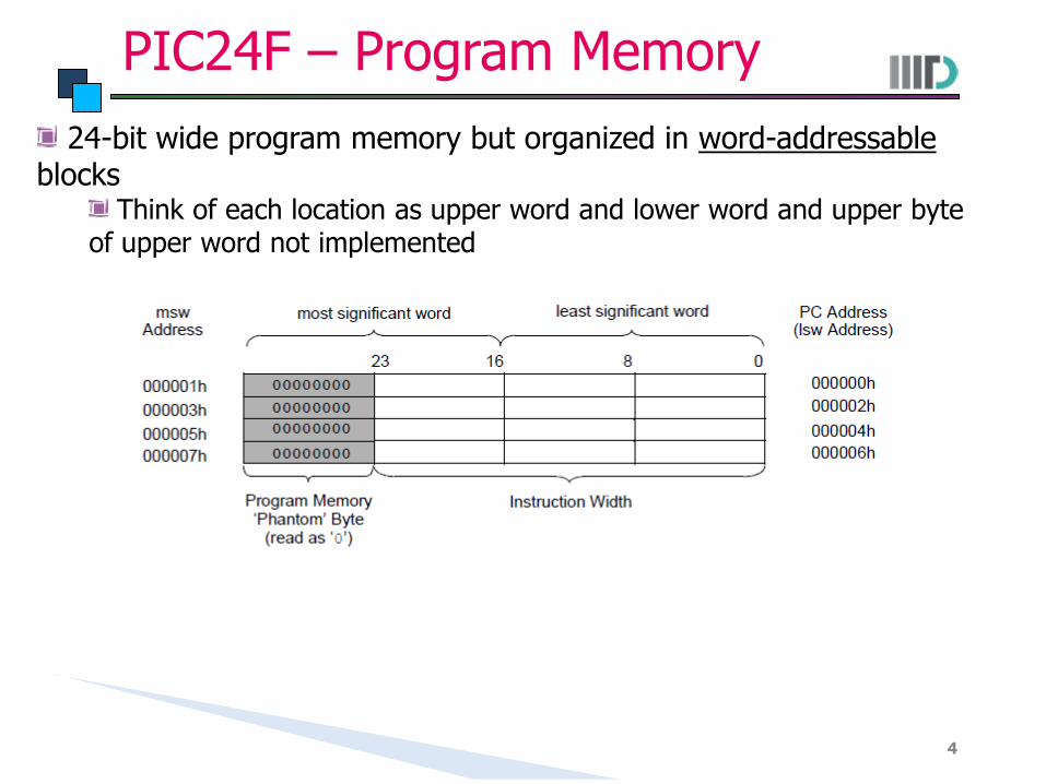
PIC24F – Program Memory
4
24-bit wide program memory but organized in word-addressable blocks
Think of each location as upper word and lower word and upper byte of upper word not implemented
PIC24F – Data Memory
5
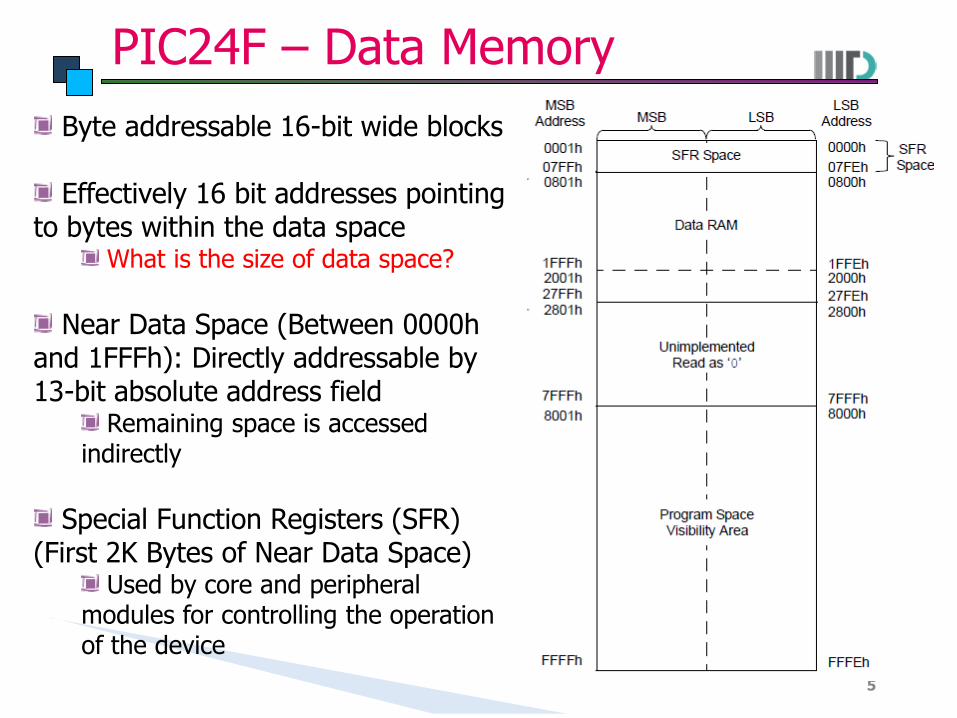
Byte addressable 16-bit wide blocks Effectively 16 bit addresses pointing
to bytes within the data space What is the size of data space?
Near Data Space (Between 0000h
and 1FFFh): Directly addressable by 13-bit absolute address field
Remaining space is accessed indirectly
Special Function Registers (SFR)
(First 2K Bytes of Near Data Space) Used by core and peripheral
modules for controlling the operation of the device
PIC24F – Data Memory
6
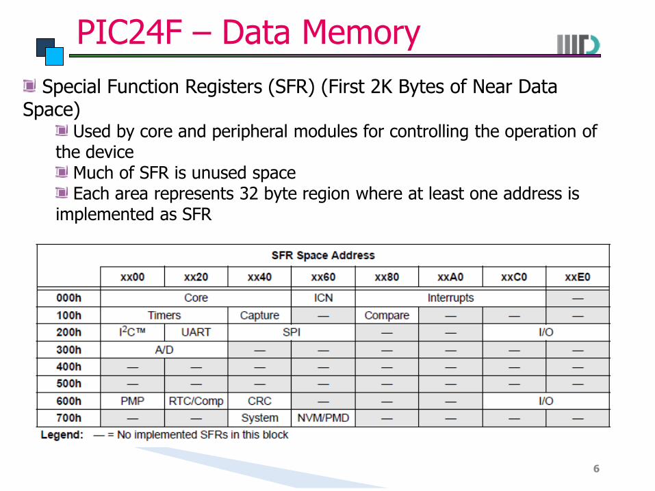
Special Function Registers (SFR) (First 2K Bytes of Near Data Space)
Used by core and peripheral modules for controlling the operation of the device
Much of SFR is unused space Each area represents 32 byte region where at least one address is
implemented as SFR
Pinout – ATxmega128A1
7
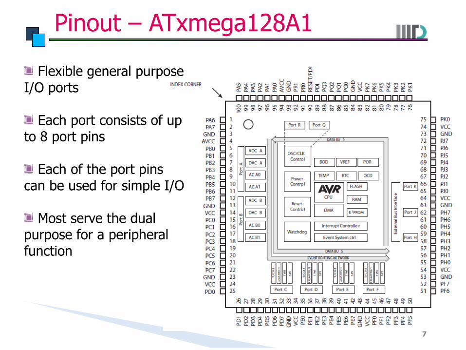
Flexible general purpose I/O ports
Each port consists of up
to 8 port pins Each of the port pins
can be used for simple I/O Most serve the dual
purpose for a peripheral function
ATxmega128A1 – Configuring the Pin
8
4 I/O memory address locations allocated for each port Data Direction Register - DIR (R/W) Data Output Value Register - OUT (R/W) Data Input Value Register - IN (Read Only) Pin Configuration Register – PINnCTRL
DIRn bit in DIRn Register selects the direction of this pin DIRn as logic 1 implies corresponding pin of that port is
configured as output pin DIRn as logic 0 implies corresponding pin of that port is
configured as input pin E.g. DIR for Port A=0xF0
Port A : Pin 0-3 - Input Pin 4-7 - Output
ATxmega128A1 – Configuring the Pin
9
When direction is set as output: OUTn bit in OUT Register is used to set the value of the pin DIRC = 0xFF //Set all Port C pins to output OUTC = 0xF0 //Set first 4 pins of Port C low and next 4 pins high
When direction is set as input: INn bit in IN Register gives the value read on that pin E.g. foo = PIND //Store the value of PORTD pins in foo
PINnCTRL is used for additional I/O pin configuration E.g. inverted I/O (Bit6) E.g. Input sense configuration (Bit2:0)
ATxmega128A1 – Input Sense Configuration
10
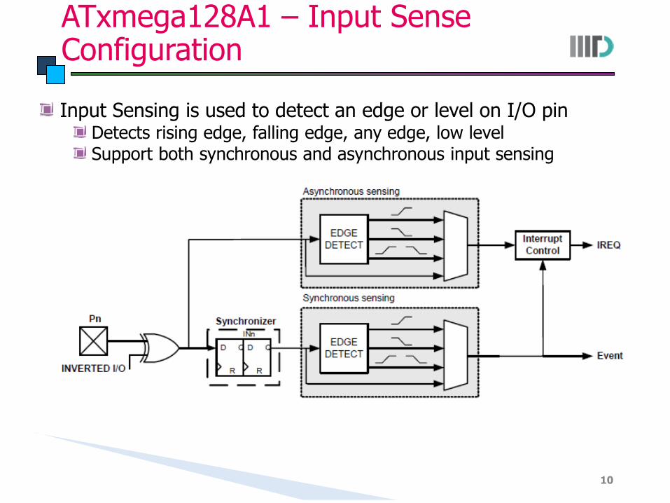
Input Sensing is used to detect an edge or level on I/O pin Detects rising edge, falling edge, any edge, low level Support both synchronous and asynchronous input sensing
ATxmega128A1 – Port Alternate Functions
11
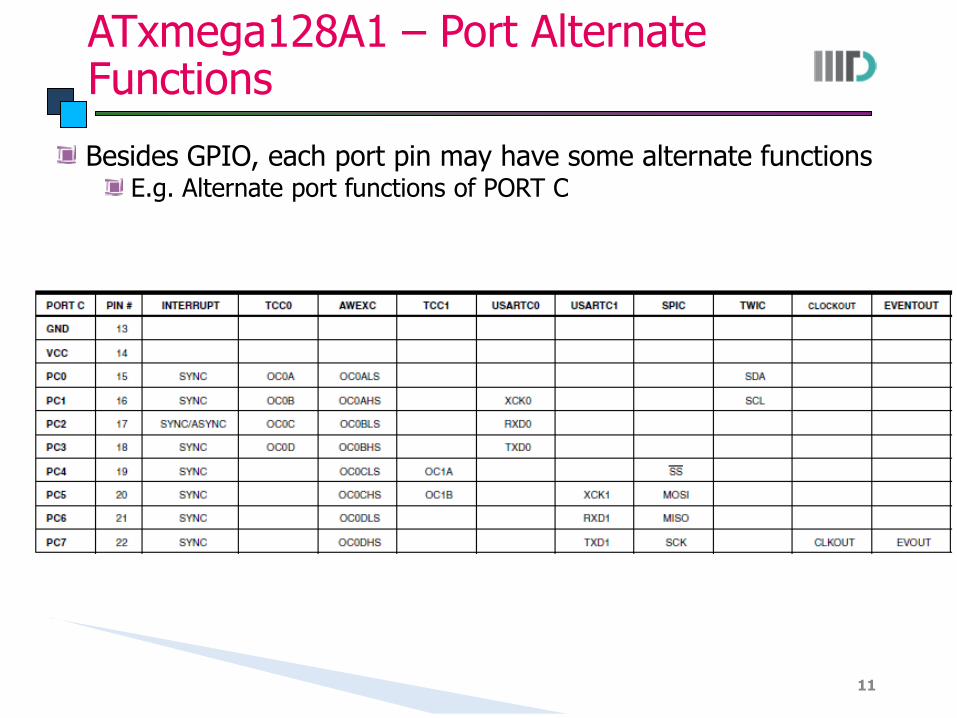
Besides GPIO, each port pin may have some alternate functions E.g. Alternate port functions of PORT C
Pinout – PIC24FJ256GA110
12
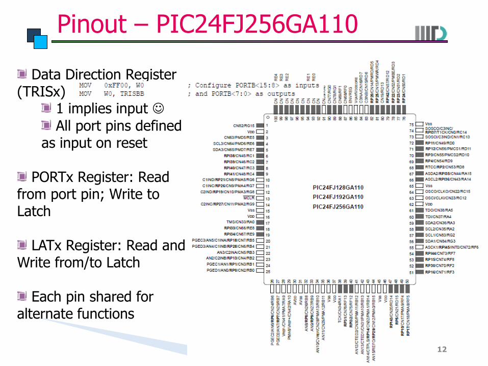
Data Direction Register (TRISx)
1 implies input
All port pins defined as input on reset
PORTx Register: Read
from port pin; Write to Latch
LATx Register: Read and
Write from/to Latch Each pin shared for
alternate functions
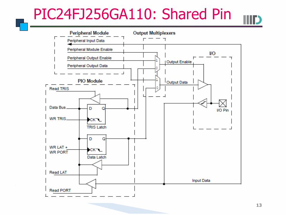
PIC24FJ256GA110: Shared Pin
13
PIC24FJ256GA110: Peripheral Pin Select
14
Operates over a fixed subset of digital I/O pins Users can independently map the input and/or output of any of
the many digital peripherals to any of these pins Peripheral Pin Select happens in software and typically does not
require the software to be reprogrammed Up to 46 pins available
Up to 32 re-mappable I/O pins (RP0 – RP31) Up to 14 re-mappable input only pins (RPI32 – RPI45)
Pin select peripherals are not associated with any default pin set Input configuration:
Each input pin for each of the configurable peripheral assigned a register with 6 bit field that is to be programmed – Why 6 bits?
Xmega-A1: System Control and Reset
15
I/O ports of AVR are immediately set to their initial state when a reset source gets active and the program starts execution from the Reset Vector
After all Reset sources have gone inactive, a delay counter is invoked, stretching the internal reset
Allows power to reach a stable value before normal operation begins
Time out period defined by user In normal operation device starts running from reset vector address
(typically 0)
Reset functionality is asynchronous – No running system clock is required to reset the system
Xmega-A1 : System Control and Reset
16
Reset Sources Power on Reset: MCU Reset when supply voltage is below the power
on reset threshold (VPOT) External Reset: Low level present on RESET pin for longer than
minimum pulse length Watchdog System Reset: On expiry of watchdog timer, when enabled Brown-out Reset: When supply voltage is less than Brown-out reset
threshold (VBOT) and Brown-out Detector enabled Software Reset: System Reset from software PDI Reset: Reset the device during external programming and
debugging
Reset Status Register shows the cause of Reset
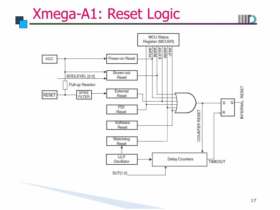
Xmega-A1: Reset Logic
17
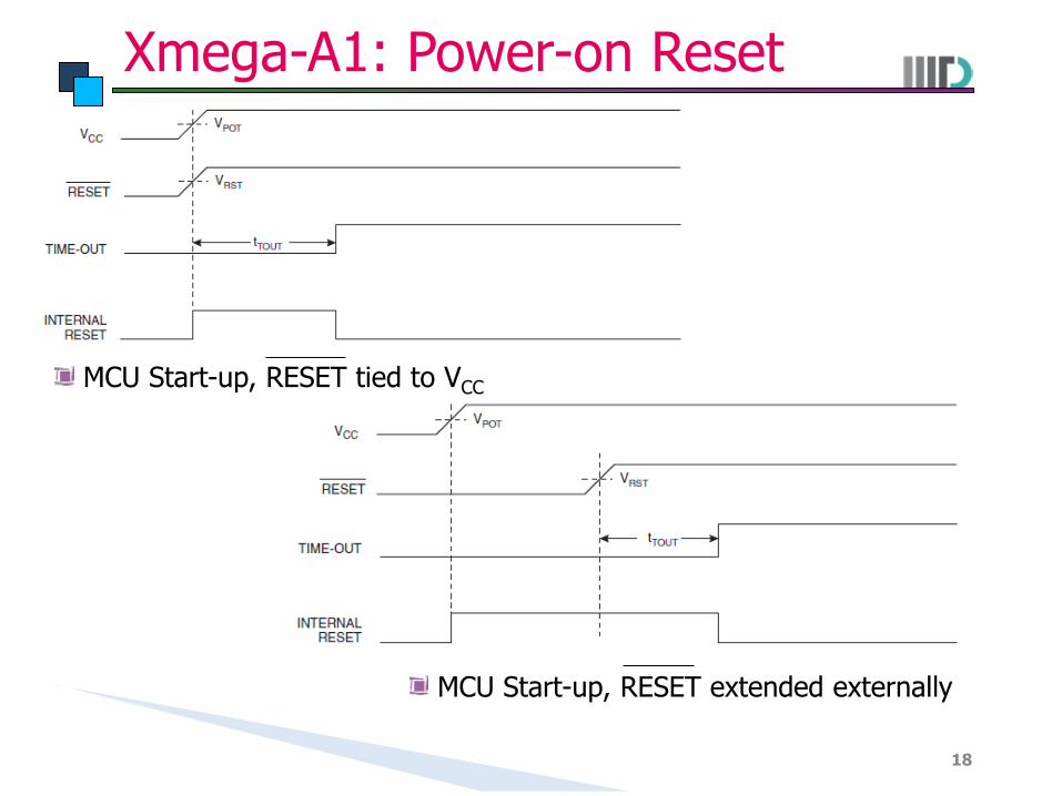
Xmega-A1: Power-on Reset
18
MCU Start-up, RESET tied to VCC
MCU Start-up, RESET extended externally
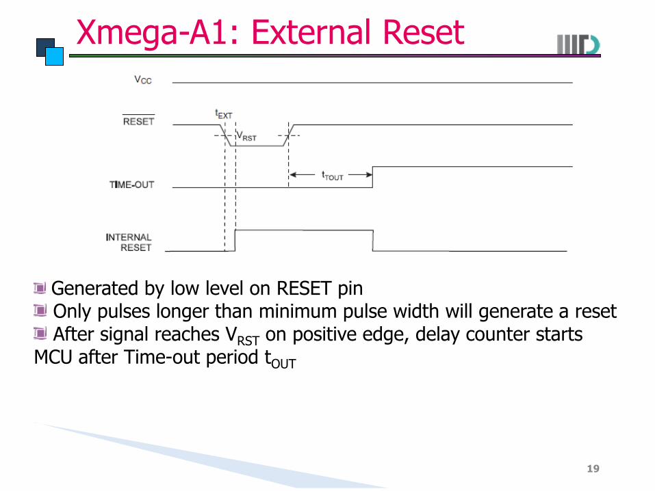
Xmega-A1: External Reset
19
Generated by low level on RESET pin Only pulses longer than minimum pulse width will generate a reset After signal reaches VRST on positive edge, delay counter starts
MCU after Time-out period tOUT
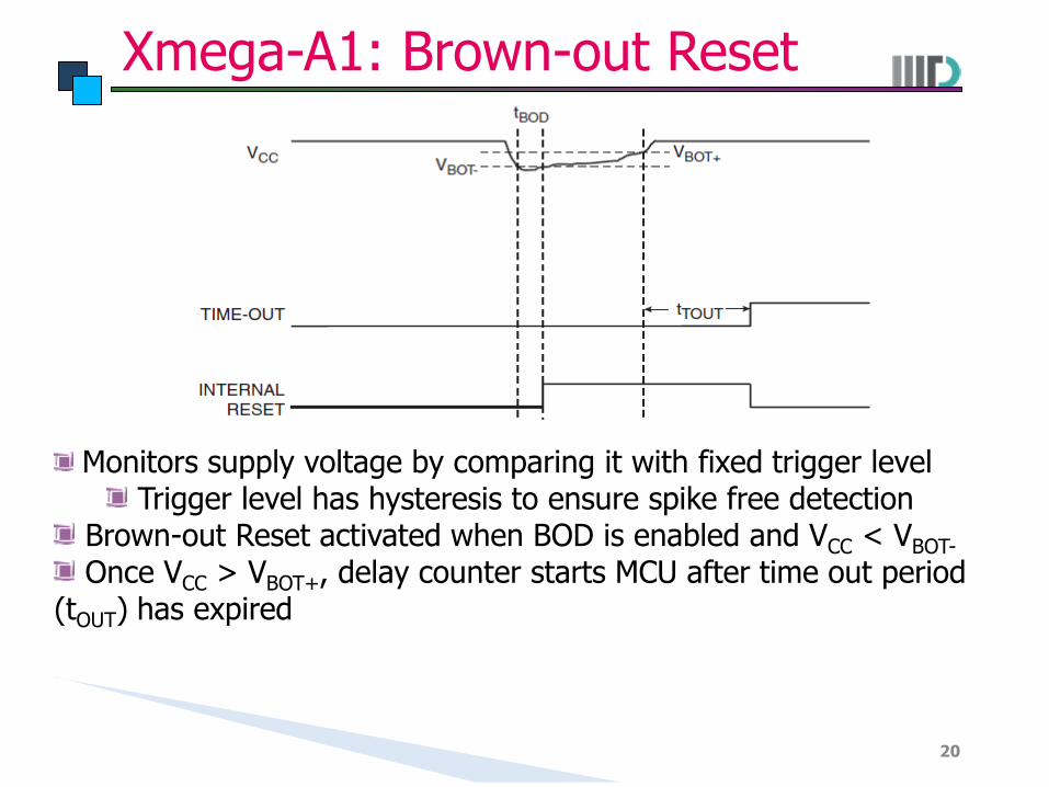
Xmega-A1: Brown-out Reset
20
Monitors supply voltage by comparing it with fixed trigger level Trigger level has hysteresis to ensure spike free detection
Brown-out Reset activated when BOD is enabled and VCC < VBOT-
Once VCC > VBOT+, delay counter starts MCU after time out period (tOUT) has expired
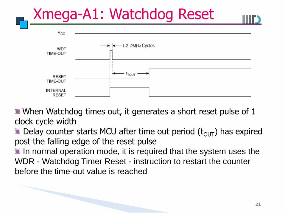
Xmega-A1: Watchdog Reset
21
When Watchdog times out, it generates a short reset pulse of 1 clock cycle width
Delay counter starts MCU after time out period (tOUT) has expired post the falling edge of the reset pulse
In normal operation mode, it is required that the system uses the
WDR - Watchdog Timer Reset - instruction to restart the counter
before the time-out value is reached
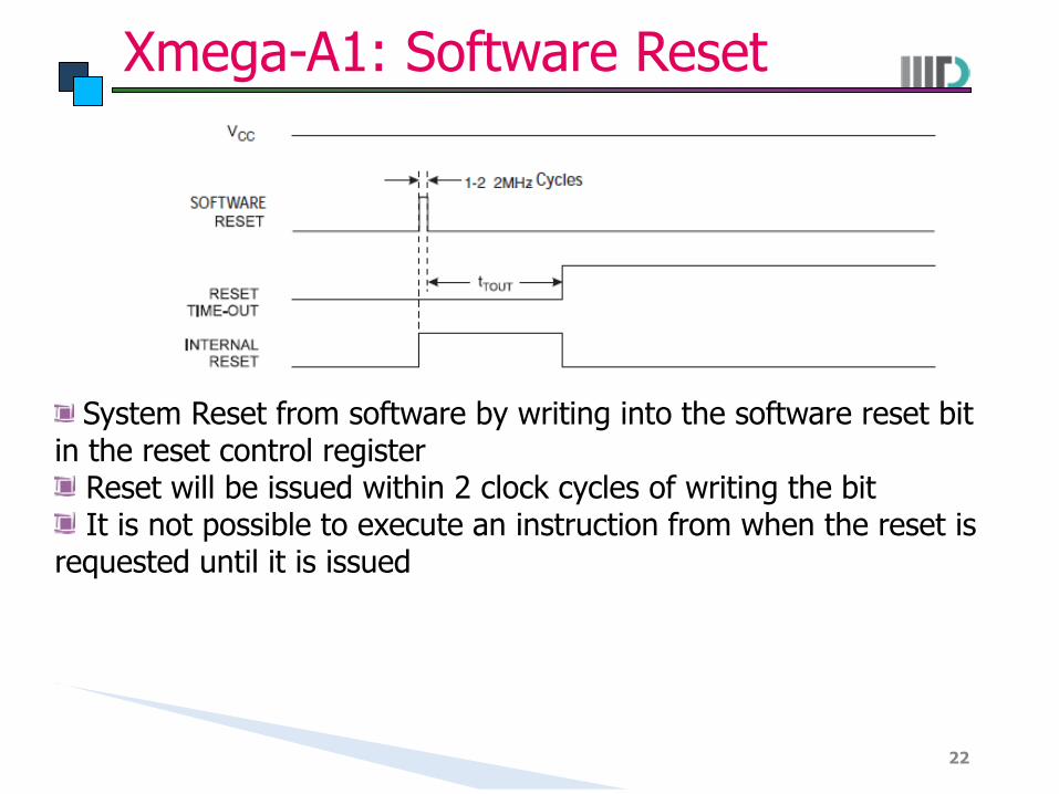
Xmega-A1: Software Reset
22
System Reset from software by writing into the software reset bit in the reset control register
Reset will be issued within 2 clock cycles of writing the bit It is not possible to execute an instruction from when the reset is
requested until it is issued
Xmega-A1: PDI Reset
23
Used to reset the device during external programming and debugging
Accessible only from external programmers and debuggers

What did you learn today?
24
On a small sheet of paper, give me a short (2-3 sentences) description of what you learned today
You can use it to give any broad comments on the class as well