microfabrication technologies · 2019-01-30 · jithin k francis,asst prof,dept of mechanical...
TRANSCRIPT

Jithin K Francis,Asst Prof,Dept of Mechanical Engineering ,RSET
MICROFABRICATION
TECHNOLOGIES
1. Microsystem Products
2. Microfabrication Processes

Jithin K Francis,Asst Prof,Dept of Mechanical Engineering ,RSET
Relative Sizes in Microtechnology
and Nanotechnology

Jithin K Francis,Asst Prof,Dept of Mechanical Engineering ,RSET
Design Trend and Terminology
Miniaturization of products and parts, with features
sizes measured in microns (10-6 m) or smaller
Microelectromechanical systems (MEMS) -
miniature systems consisting of both electronic
and mechanical components
Microsystem technology (MST) - refers to the
products as well as the fabrication technologies
Nanotechnology - even smaller entities whose
dimensions are measured in nanometers (10-9 m)

Jithin K Francis,Asst Prof,Dept of Mechanical Engineering ,RSET
Advantages of Microsystem
Products
Less material usage
Lower power requirements
Greater functionality per unit space
Accessibility to regions that are forbidden to larger
products
In most cases, smaller products should mean lower
prices because less material is used

Jithin K Francis,Asst Prof,Dept of Mechanical Engineering ,RSET
Types of Microsystem Devices
Microsensors
Microactuators
Microstructures and microcomponents
Microsystems and micro-instruments

Jithin K Francis,Asst Prof,Dept of Mechanical Engineering ,RSET
Microsensors
A sensor is a device that detects or measures some
physical phenomenon such as heat or pressure
Most microsensors are fabricated on a silicon substrate
using the same processing technologies as those used
for integrated circuits
Microsensors have been developed to measure force,
pressure, position, speed, acceleration, temperature,
flow, and various optical, chemical, environmental, and
biological variables

Jithin K Francis,Asst Prof,Dept of Mechanical Engineering ,RSET
Microactuators
An actuator converts a physical variable of one type
into another type, and the converted variable usually
involves some mechanical action
An actuator causes a change in position or the
application of force
Examples of microactuators: valves, positioners,
switches, pumps, and rotational and linear motors

Jithin K Francis,Asst Prof,Dept of Mechanical Engineering ,RSET
Microstructures and
Microcomponents
Micro-sized parts that are not sensors or actuators
Examples: microscopic lenses, mirrors, nozzles,
gears, and beams
These items must be combined with other
components in order to provide a useful function

Jithin K Francis,Asst Prof,Dept of Mechanical Engineering ,RSET
Microscopic Gear
and Human Hair
Image by scanning electron microscope - gear is high-density
polyethylene molded by a process similar to LIGA (photo courtesy of
W. Hung, Texas A&M U., and M. Ali, Nanyang Tech. U).

Jithin K Francis,Asst Prof,Dept of Mechanical Engineering ,RSET
Microsystems and micro-
instruments
Integration of several of the preceding components
with the appropriate electronics package into a
miniature system or instrument
Products tend to be very application-specific
Examples: microlasers, optical chemical
analyzers, and microspectrometers
The economics of manufacturing these kinds of
systems have made commercialization difficult
Jithin K Francis,Asst Prof,Dept of Mechanical Engineering ,RSET
Industrial Applications of
Microsystems
Ink-jet printing heads
Thin-film magnetic heads
Compact disks
Automotive components
Medical applications
Chemical and environmental applications
Other applications
Jithin K Francis,Asst Prof,Dept of Mechanical Engineering ,RSET
Ink-Jet Printing Heads
Currently one of the largest applications of
microsystems
A typical ink-jet printer uses up several cartridges
each year
Today’s ink-jet printers have resolutions of 1200 dots
per inch (dpi)
This resolution converts to a nozzle separation
of only about 21 m
Certainly in the microsystem range

Jithin K Francis,Asst Prof,Dept of Mechanical Engineering ,RSET
Resistance heater boils ink to create plume that
forces drop to be expelled onto paper
Ink-Jet Printer Head

Jithin K Francis,Asst Prof,Dept of Mechanical Engineering ,RSET
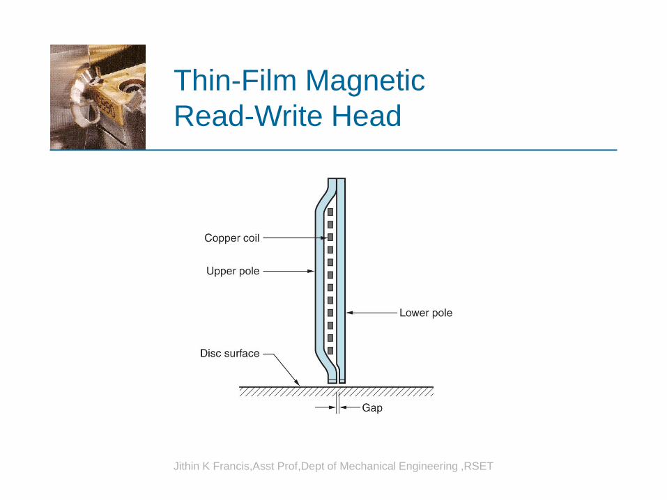
Thin-Film Magnetic Heads
Read-write heads are key components in magnetic storage devices
Reading and writing of magnetic media with higher bit densities limited by the size of the read-write head
Development of thin-film magnetic heads was an important breakthrough not only in digital storage technology but microfabrication technologies as well
Thin-film read-write heads are produced annually in hundreds of millions of units.
Jithin K Francis,Asst Prof,Dept of Mechanical Engineering ,RSET
Thin-Film Magnetic
Read-Write Head

Jithin K Francis,Asst Prof,Dept of Mechanical Engineering ,RSET
Automotive Components
Micro-sensors and other micro-devices are widely used in modern automobiles
Between 20 and 100 sensors are installed in a modern automobile
Functions include cruise control, anti-lock braking systems, air bag deployment, automatic transmission control, power steering, all-wheel drive, automatic stability control, and remote locking and unlocking
In 1970 there were virtually no on-board sensors

Jithin K Francis,Asst Prof,Dept of Mechanical Engineering ,RSET
Medical Applications
A driving force for microscopic devices is the principle
of minimal-invasive therapy
Small incisions or even available body orifices to
access the medical problem
Standard medical practice today is to use endoscopic
examination accompanied by laparoscopic surgery for
hernia repair and removal of gall bladder and appendix
Similar procedures are used in brain surgery, operating
through small holes drilled in skull

Jithin K Francis,Asst Prof,Dept of Mechanical Engineering ,RSET
Microfabrication Processes
Many MST products are based on silicon - Why?
Microdevices often include electronic circuits, so
both the circuit and the device can be made on the
same substrate
Silicon has good mechanical properties:
High strength and elasticity, good hardness,
and relatively low density
Techniques to process silicon are well
established from processing of ICs

Jithin K Francis,Asst Prof,Dept of Mechanical Engineering ,RSET
Other Materials and MST
Processing
MST often requires other materials in addition to
silicon to obtain a particular microdevice
Example: microactuators often consist of several
components made of different materials
Thus, microfabrication techniques consist of more
than just silicon processing:
LIGA process
Other conventional and nontraditional processes
performed on microscopic scale
Jithin K Francis,Asst Prof,Dept of Mechanical Engineering ,RSET
Silicon Layer Processes
First application of silicon in MST was in the
fabrication of piezoresistive sensors to measure
stress, strain, and pressure in the early 1960s
Silicon is now widely used in MST to produce
sensors, actuators, and other microdevices
The basic processing technologies are those used to
produce integrated circuits
However, there are certain differences between
processing of ICs and fabrication of microdevices

Jithin K Francis,Asst Prof,Dept of Mechanical Engineering ,RSET
Microfabrication vs.
IC Fabrication
Aspect ratios (height-to-width ratio of the features) in
microfabrication are generally much greater than in
IC fabrication
The device sizes in microfabrication are often much
larger than in IC processing
The structures produced in microfabrication often
include cantilevers and bridges and other shapes
requiring gaps between layers
These features are not found in integrated circuits

Introduction/Outline
- What Are MEMS?
- Components of MEMS
- Applications
- Summary
Jithin K Francis,Asst Prof,Dept of Mechanical Engineering ,RSET
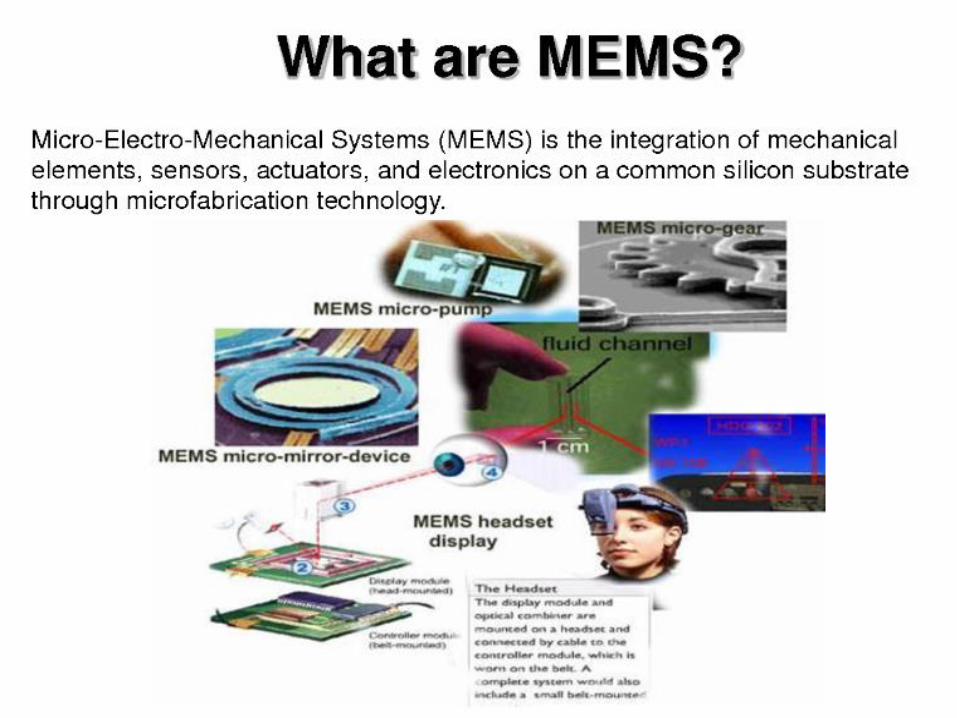

What are MEMS?
• Micro - Small size, microfabricated structures
• Electro - Electrical signal /control ( In / Out )
• Mechanical - Mechanical functionality ( In / Out )
• Systems - Structures, Devices, Systems


What are MEMS?
• Made up of components between 1-100 micrometers in size
• Devices vary from below one micron up to several mm
• Functional elements of MEMS are miniaturized structures, sensors,
actuators, and microelectronics
• One main criterion of MEMS is that there are at least some elements
that have mechanical functionality, whether or not they can move

Microelectronics:
• “brain” that receives, processes, and makes decisions
• data comes from microsensors
Microsensors:
• constantly gather data from environment
• pass data to microelectronics for processing
• can monitor mechanical, thermal, biological, chemical optical, and
magnetic readings
Microactuator:
• acts as trigger to activate external device
• microelectronics will tell microactuator to activate device
Microstructures:
• extremely small structures built onto surface of chip
• built right into silicon of MEMS
Components

Why Micro machine?
Minimize energy and materials use in manufacturing
• Redundancy and arrays
• Integration with electronics
• Reduction of power budget
• Faster devices
• Increased selectivity and sensitivity
• Cost/performance advantages
• Improved reproducibility (batch fabrication)
• Improved accuracy and reliability
• Minimally invasive (e.g. pill camera)

Factors to Consider
Establish need in light of conventional approaches
(faster, smaller, cheaper)
– Does the MEMS solution provide a significant cost reduction?
– Does it enable a new function or level of performance that cannot be
achieved otherwise?
– Does the market justify the development of a MEMS approach? Can
conventional machining or plastic molding techniques be used?
– Does the cost analysis include package & test?
Understand the basic physics and operating principles,
including scaling laws
– Increased surface-to-volume ratio
– Actuation forces
– Thermal transport
• Understand the important issues in designing
macroscopic and microscopic solutions

Factors to Consider
Can you use an existing “standard” process?
– If not, can you design a simple and reasonably priced
fabrication process?
Consider the issues of packaging at the outset:
– Can existing packages be used or adapted?
– Reliability issues (e.g. hermetically sealed)?
Estimate the final cost of the ready-to-use device
– Difficult to get cost data out of foundry for custom
process. Will depend sensitively on volume and yield.
This is really difficult to access!
– Include the cost of packaging
– Include the cost of testing

Where Are MEMS?
Smartphones, tablets, cameras, gaming devices, and
many other electronics have MEMS technology
inside of them
Jithin K Francis,Asst Prof,Dept of Mechanical Engineering ,RSET
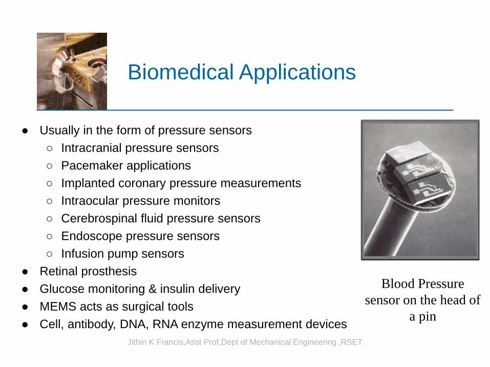
Biomedical Applications
● Usually in the form of pressure sensors
○ Intracranial pressure sensors
○ Pacemaker applications
○ Implanted coronary pressure measurements
○ Intraocular pressure monitors
○ Cerebrospinal fluid pressure sensors
○ Endoscope pressure sensors
○ Infusion pump sensors
● Retinal prosthesis
● Glucose monitoring & insulin delivery
● MEMS acts as surgical tools
● Cell, antibody, DNA, RNA enzyme measurement devices
Jithin K Francis,Asst Prof,Dept of Mechanical Engineering ,RSET
Blood Pressure
sensor on the head of
a pin

In the Car
Jithin K Francis,Asst Prof,Dept of Mechanical Engineering ,RSET
Key Concepts
1. MEMS are made up of microelectronics,
microactuators, microsensors, and microstructures.
2. The three basic steps to MEMS fabrication are:
deposition, patterning, and etching.
3. Chemical wet etching is popular because of high
etch rate and selectivity.
4. The benefits of using MEMS: speed, power
consumption, size, system integration(all on one
chip).
Jithin K Francis,Asst Prof,Dept of Mechanical Engineering ,RSET
Summary
Micro-Electro-Mechanical Systems are 1-100 micrometer
devices that convert electrical energy to mechanical
energy and vice-versa.
The three basic steps to MEMS fabrication are deposition,
patterning, and etching.
Due to their small size, they can exhibit certain
characteristics that their macro equivalents can’t.
MEMS produce benefits in speed, complexity, power
consumption, device area, and system integration.
These benefits make MEMS a great choice for devices in
numerous fields.Jithin K Francis,Asst Prof,Dept of Mechanical Engineering ,RSET

Jithin K Francis,Asst Prof,Dept of Mechanical Engineering ,RSET
LIGA Process/LIGA Lithography
LIGA is a German acronym that stands for
Lithographie, Galvanoformung and Abformung.
When translated it means lithography, electroplating
and molding.

Jithin K Francis,Asst Prof,Dept of Mechanical Engineering ,RSET
LIGA Process
An important technology of MST
Developed in Germany in the early 1980s
LIGA stands for the German words
LIthographie (in particular X-ray lithography)
Galvanoformung (translated electrodeposition or
electroforming)
Abformung (plastic molding)
The letters also indicate the LIGA process sequence
Jithin K Francis,Asst Prof,Dept of Mechanical Engineering ,RSET
Background
LIGA is a three stage micromachining technology
used to manufacture high aspect ratio
microstructures.
Originally LIGA technology was researched in
Germany in order to be used for the separation of
uranium isotopes.

Jithin K Francis,Asst Prof,Dept of Mechanical Engineering ,RSET
Background
Two main types of LIGA Technology: X-ray LIGA and
Extreme Ultraviolet (EUV) LIGA.
X-ray LIGA can fabricate with great precision high
aspect ratio microstructures.
EUV LIGA can fabricate lower quality
microstructures.

Jithin K Francis,Asst Prof,Dept of Mechanical Engineering ,RSET
LIGA is a hybrid fabrication technique
The LIGA Process
Lithography
Electron beam lithography
Focused ion beam lithography
Optical and exciter laser lithography
Deep X-ray lithography using synchrotron radiation
Electroplating
metalized layer (seed layer)
Molding
Machining process to remove overplated metal region
LIGA Process
Jithin K Francis,Asst Prof,Dept of Mechanical Engineering ,RSET
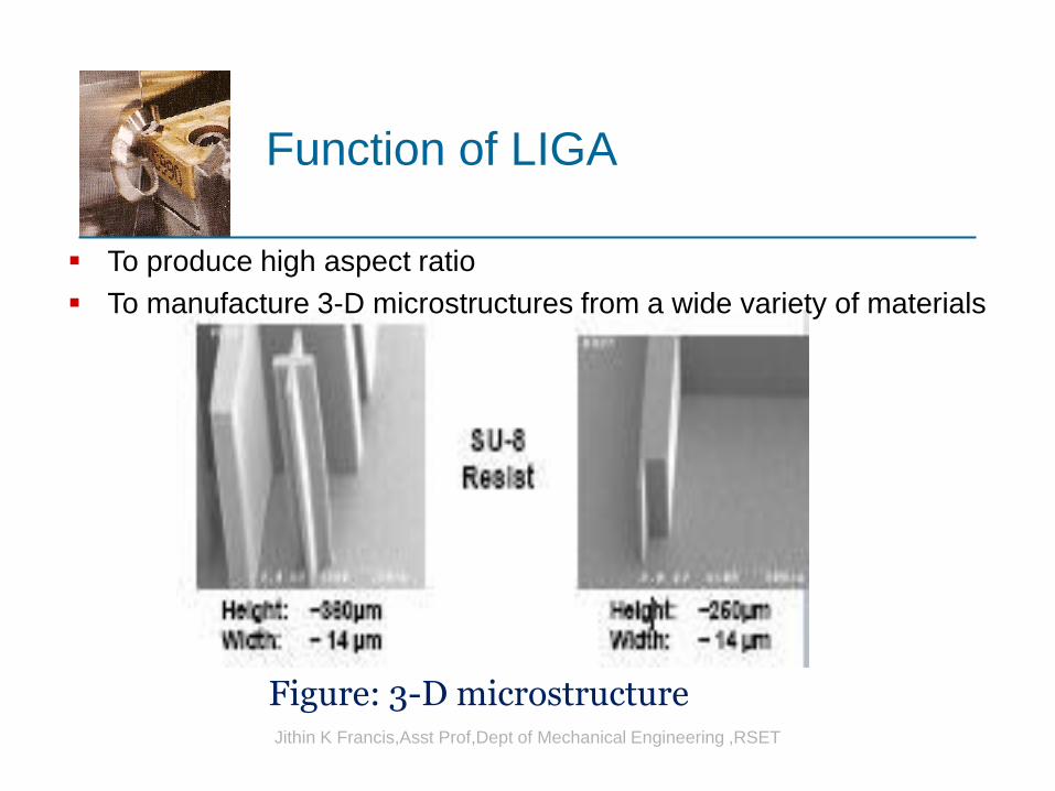
To produce high aspect ratio
To manufacture 3-D microstructures from a wide variety of materials
Function of LIGA
Figure: 3-D microstructure

Jithin K Francis,Asst Prof,Dept of Mechanical Engineering ,RSET
Processing Steps in LIGA

Jithin K Francis,Asst Prof,Dept of Mechanical Engineering ,RSET
Step 1:
-Deposition of Adhesion
-Seed layer
Processing Steps in LIGA

Jithin K Francis,Asst Prof,Dept of Mechanical Engineering ,RSET
Step 2:
-resist coating
Processing Steps in LIGA

Jithin K Francis,Asst Prof,Dept of Mechanical Engineering ,RSET
Step 3:
-expose the PMMA resist
Processing Steps in LIGA

Jithin K Francis,Asst Prof,Dept of Mechanical Engineering ,RSET
Step 4:
-development of the exposed resist
Processing Steps in LIGA

Jithin K Francis,Asst Prof,Dept of Mechanical Engineering ,RSET
Electroplating is a process to fill in the voids between the polymeric
features.
Step 5:
-metal plating
Processing Steps in LIGA
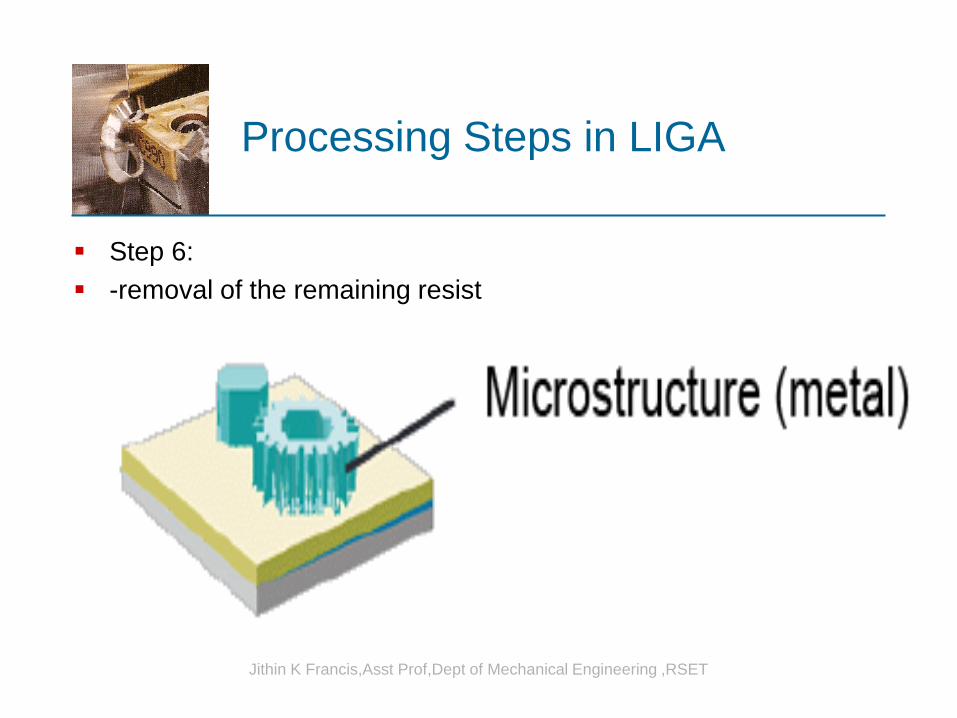
Jithin K Francis,Asst Prof,Dept of Mechanical Engineering ,RSET
Step 6:
-removal of the remaining resist
Processing Steps in LIGA

Jithin K Francis,Asst Prof,Dept of Mechanical Engineering ,RSET
Molding is process of machining the overplated region filling the
microstructure
Step 7:
Processing Steps in LIGA

Jithin K Francis,Asst Prof,Dept of Mechanical Engineering ,RSET

Jithin K Francis,Asst Prof,Dept of Mechanical Engineering ,RSET

Jithin K Francis,Asst Prof,Dept of Mechanical Engineering ,RSET

Jithin K Francis,Asst Prof,Dept of Mechanical Engineering ,RSET
Advantages of LIGA
LIGA is a versatile process – it can produce parts by
several different methods
High aspect ratios are possible (large height-to-width
ratios in the fabricated part)
Wide range of part sizes is feasible - heights ranging
from micrometers to centimeters
Close tolerances are possible
Jithin K Francis,Asst Prof,Dept of Mechanical Engineering ,RSET
Disadvantages of LIGA
LIGA is a very expensive process
Large quantities of parts are usually required to
justify its application
LIGA uses X-ray exposure
Human health hazard

Jithin K Francis,Asst Prof,Dept of Mechanical Engineering ,RSET
Other Microfabrication
Processes
Soft lithography
Nontraditional and traditional processes and rapid prototyping adapted for microfabrication
Photochemical machining
Electroplating, electroforming, electroless plating
Electric discharge machining
Electron beam machining
Ultrasonic machining
Microstereolithography