microlaser assisted diamond turning of precision silicon
TRANSCRIPT

Microlaser assisted diamond turningof precision silicon optics
Hossein ShahinianJayesh NavareDmytro ZaytsevDeepak Ravindra
Hossein Shahinian, Jayesh Navare, Dmytro Zaytsev, Deepak Ravindra, “Microlaser assisted diamond turningof precision silicon optics,” Opt. Eng. 58(9), 092607 (2019), doi: 10.1117/1.OE.58.9.092607.
Downloaded From: https://www.spiedigitallibrary.org/journals/Optical-Engineering on 24 Jan 2022Terms of Use: https://www.spiedigitallibrary.org/terms-of-use
Microlaser assisted diamond turning of precisionsilicon optics
Hossein Shahinian,* Jayesh Navare, Dmytro Zaytsev, and Deepak RavindraMicro-LAM Inc., Portage, Michigan, United States
Abstract. The application of microlaser assisted machining of precision optical components made of opticalgrade single-crystal Si is reviewed. An optical raytracing model is developed and used for predicting the laserinteraction with the workpiece. Optical characterization of the system is shown to be in good agreement with thatpredicted by the model. Using the information from the simulation and experimental validation, the laser-assisteddiamond turning of single-crystal Si samples is shown to have exhibited little to no brittle fracture on the surfaceand the potential of extending the diamond tooling life by 150%. © 2019 Society of Photo-Optical Instrumentation Engineers(SPIE) [DOI: 10.1117/1.OE.58.9.092607]
Keywords: infrared optics; lasers; diamond turning.
Paper 190140SS received Jan. 29, 2019; accepted for publication Mar. 27, 2019; published online Apr. 11, 2019.
1 IntroductionThe advent of ultraprecision machining (UPM) centers hasbeen a significantly enabling technology in producing pre-cise, optically smooth surfaces.1 The key advantages ofUPM are mainly the fast convergence and high determinismof the process.2 Additionally, manufacturing complex free-form and aspherical optical components is far more conven-ient using UPM than that of traditional manufacturingtechniques, i.e., grinding and polishing.3 The primary limi-tation in using UPM is the limited number of materials thatcan be classified as machinable with such technologies.4
The machinability refers to the ability of UPM in achiev-ing optically smooth surfaces (roughness values <10 nmRMS), with small figure errors (smaller than 50 nm rootmean square irregularity). Typically, single-crystal diamondtools are used, as diamond is the hardest material, offeringthe most robust tool. The tool is machined with a very well-defined cutting edge, combined with the application of ahigh degree of thermal stability during the process,5 as wellas isolation from external vibration sources, enabling thehigh-positional repeatability of the UPM.6,7
Although initially UPM of soft metals in single-point dia-mond turning (SPDT) configuration was considered a greatbreakthrough in the optical fabrication realm, more recentlythe SPDT of hard and brittle infrared (IR) materials hasgained traction within the community. Of great interest is themachining of single-crystal silicon (Si) optics. Si has a rel-atively high index of refraction, and with transmission ratesof over 60%, it provides a great opportunity in designing IRoptical components.8,9 The alternative to Si is the much moreexpensive germanium (Ge) optics. Si is both lighter andcheaper than Ge, as well as its higher hardness offers supe-rior mechanical properties to that of Ge. Nevertheless, due toSi’s lower fracture toughness to hardness ratio, machiningfracture free surfaces poses a bigger challenge than Ge.10,11
Typically, the fractured surface exhibits anisotropic surfacefinish on zones along the cleavage planes.12,13 These zonescan be indicative of highly deformed crystal grains
underneath the surface and are detrimental to the optical per-formance and mechanical integrity of the optic.14
The other key challenge in machining Si is the muchhigher tool wear rates compared to those in machiningGe.15 The wear rates are a function of the material hardness,process temperatures, and chemical composition of theworkpiece in SPDT.4 Although some have suggested the useof flooded coolants, this negatively impacts the final formachievable on the part.
Many articles have investigated the effect of variousprocess parameters on promoting a ductile cutting regimeon Si.16–20 Most of these techniques lead to severe limitationson workpiece sizes achievable. In this paper, an alternativeapproach is used, that is, the application of a laser beam dur-ing SPDTand exactly at the cutting edge of the single-crystaldiamond tool.
2 Summary of the μ-LAM ProcessThe microlaser assisted machining (μ-LAM) process lever-ages a laser emission beam at the cutting interface betweentool and workpiece to facilitate a more ductile cuttingregime.21 The laser is directed through a series of optics,which can then pass through a polished optical surface orintegrated lens on the back face of the diamond. The laserposition can be finely adjusted and placed precisely at thediamond tool edge, as shown in Fig. 1.
The laser light is absorbed by the workpiece material by60% of the total irradiance. The absorption of the lasercauses the material to be heated locally. As outlined by manyarticles,22 single-crystal Si exhibits thermal annealing fortemperatures near 1000°C. That said the annealing temper-ature is much lower in the presence of high-pressure values(>10 GPa).23 Given the small contact area between the cut-ting tool and the workpiece surface during SPDT, such pres-sures are common to attain.24 Thus it is speculated that thelaser heating under the high pressures of SPDT promotes theductile cutting of Si by annealing the surface.25
The laser absorption and heating process are localizedonly to an area <300 μm2 at the vicinity of the tool tip.
*Address all correspondence to Hossein Shahinian, E-mail: [email protected] 0091-3286/2019/$25.00 © 2019 SPIE
Optical Engineering 092607-1 September 2019 • Vol. 58(9)
Optical Engineering 58(9), 092607 (September 2019)
Downloaded From: https://www.spiedigitallibrary.org/journals/Optical-Engineering on 24 Jan 2022Terms of Use: https://www.spiedigitallibrary.org/terms-of-use

Therefore, there is no bulk heating of the material, and theheat introduced is then immediately dissipated in the chipsof removed material. This localized heating is crucial inachieving the desirable form error of the surface.
The optical raytracing model from which the laser powerand irradiance can be predicted were generated. The predic-tions were complimented by experimental measurements.Machining experiments were conducted to verify three as-pects of the μ-LAM process: (1) the laser heating is localizedand repeatable, (2) the laser heating does promote a higherdegree of ductile cutting, and (3) the more ductile regimemachining increases the tool life during machining.
3 Experimental Equipment
3.1 Test Bed
The testing was done on an ultraprecision lathe, a PrecitechNanoform 250 Ultra, see Fig. 2(a). The lathe consists of twocomputerized numerically controlled axes, X and Z (bothhave a travel range of 220 mm), as well as an active hydraulicdamping system to minimize the vibrations induced duringthe machining. The workpiece was mounted to an HS-150high-speed air bearing spindle. The spindle had a maximumRPM of 15,000. The positional repeatability of the machinewas <10 nm.
A custom-made toolpost, the Optimus, was affixed to themachine table as depicted in Fig. 2(b). The toolpost con-sists of a rigid tool holder and a carriage that holds the laser
delivery optical system (LDOS). The LDOS was comprisedof a collimator and a series of optical elements, see Fig. 3,directing the laser toward the cutting edge of the diamondtool. The carriage also incorporates micrometers that allowthe proper calibration and alignment of the laser beam posi-tion with respect to the tool. The tool holder used a differ-ential screw mechanism to align the tool to the centerline ofthe spindle. The laser beam was produced in an Nd:YAGlasing medium with a wavelength of 1064 nm (IR beam).In addition, a low-power, visible, HeNe laser (red beam)was also incorporated, concentered with the Nd:YAG laserbeam, for alignment purposes. The complete module wascontrolled with the laser control station (LCS) depicted inFig. 2(a). The LCS had the ability of changing the IR beampower by 1-W increments.
3.1.1 Diamond tools
The tools were made of single-crystal synthetic high-pressure, high-temperature diamond material. The μ-LAMprocess used a proprietary tool design that allowed the trans-mission of laser light through the tool, thereby irradiating thecutting interface. The diamond tool is described by its noseradius (the radius of curvature of the cutting edge), the rakeangle, and the clearance angle, as shown in Fig. 3. The toolsused in the experiment had nose radius of 0.3 mm, rake angleof −35 deg, clearance angle of 10 deg, and a cutting height(see Fig. 3 for cutting height) of 0.9 to 1.0 mm.
3.1.2 Laser beam alignment
To ascertain that the cutting interface received the properamount of laser power and that the laser was emittingthrough the proper region of the tool, an alignment procedurewas performed. The alignment equipment consists of amultispectral absorbing power meter and a camera imagingthe aperture of the power meter, see Fig. 4(a). The low-power, visible red beam was used to align the beam laterally.The vertical alignment of the beam was performed by meas-uring the power coming through the diamond and adjustingthe vertical micrometer to a spot that the central zone of thebeam was near the cutting edge. The beam was aligned tooutput 30% to 50% of its total power through the clearanceface of the diamond tool. It is speculated that this ratio pro-duces a more uniform distribution of the laser power alongthe cutting edge of the tool. For the cutting experiments
Fig. 1 Overview of μ-LAM process.
Fig. 2 Experimental setup: (a) LCS integrated with Precitech two-axis machining center and (b) test bedwith Optimus toolpost and Si sample.
Optical Engineering 092607-2 September 2019 • Vol. 58(9)
Shahinian et al.: Microlaser assisted diamond turning of precision silicon optics
Downloaded From: https://www.spiedigitallibrary.org/journals/Optical-Engineering on 24 Jan 2022Terms of Use: https://www.spiedigitallibrary.org/terms-of-use

reported in this paper, the power measured through the clear-ance was 2.7 W. Fig. 4(b) depicts the image of the IR beamspot on the power meter.
3.1.3 Laser spot calibration
To ensure the repeatability of the delivered laser beam at thetool tip, a calibration procedure was used. A shallow depthof field imaging camera was mounted to the toolpost andfocused onto a calibration artifact that was placed onto thefront of the toolpost, see Fig. 5. This artifact represents aknown position relative to the nominal diamond tool cuttingedge, whereby the camera was focused on. The red beam,imaged by the same camera, was then moved axially suchthat a minimum spot size was attained. The axial motionof the beam is provided by the Z axis micrometer shownin Fig. 5.
3.2 Test Sample
The sample used for the testing was a∅62 mm plano-convexsingle-crystal Si optic. The crystal lattice had h111i direc-tion. The radius of curvature of the part was 205 mm.The sample was diamond turned prior to the commencement
of the testing to ensure that the surface was free of tilt, grind-ing marks, and any other defects.
3.3 Metrology
The Si sample was subjected to two types of surface metrol-ogy, i.e., form and surface finish measurements. The formmeasurements were taken on a Taylor Hobson LuphosScan®
260 HD, a noncontact multiwavelength scanning interferom-eter. The surface finish measurements were taken using aTaylor Hobson coherence correlation interferometer (CCI).The metrics and data processing used for evaluation of formand surface finish measurements are listed in Table 1.
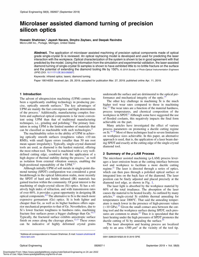
4 Raytracing ModelThe raytracing model was created in Zemax OpticStudio®.Both sequential and nonsequential raytracings were used.
4.1 Sequential Raytracing
The sequential module was used for prediction of the focus-ing spot size of the LDOS. Figure 6(a) shows the overalllayout of the optical system used in the Optimus toolpost.In Fig. 6(b), the focusing spot is calculated to be as muchas 20.94 μm.
Fig. 3 Optimus toolpost and diamond tool schematic.
Fig. 4 (a) Laser alignment accessory and (b) image of laser spot on power meter.
Fig. 5 Laser spot calibration equipment and procedure.
Optical Engineering 092607-3 September 2019 • Vol. 58(9)
Shahinian et al.: Microlaser assisted diamond turning of precision silicon optics
Downloaded From: https://www.spiedigitallibrary.org/journals/Optical-Engineering on 24 Jan 2022Terms of Use: https://www.spiedigitallibrary.org/terms-of-use
4.2 Nonsequential Raytracing
The nonsequential module is used to predict and study theexiting beam from the tip of the diamond tool and to gainmore realistic data for machining purposes. The beam wasmodeled as a Gaussian beam, with beam divergence of24.5 mrad, and a beam waist size of 24 μm. The diamondtool geometry was generated in SolidWorks® and importedto Zemax®. A total of 106 number of analysis rays were used.Due to the curved shape of the tool tip, a surface detectorwith the same curvature of the diamond tool was used.The detector had 300 radial and 300 angular zones.
5 Optical Characterization Test Bench
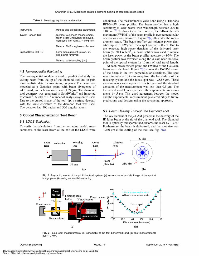
5.1 LDOS Evaluation
To verify the calculations from the raytracing model, mea-surements of the laser beam at the exit of the LDOS were
conducted. The measurements were done using a ThorlabsBP104-UV beam profiler. The beam profiler has a highsensitivity to laser beams with wavelength between 200 to1100 nm.26 To characterize the spot size, the full-width half-maximum (FWHM) of the beam profile in two perpendicularorientations was measured. Figure 7(a) illustrates the meas-urement setup. The beam profiler can tolerate power den-sities up to 10 kW∕cm2 for a spot size of ∼30 μm. Due tothe expected high-power densities of the delivered laserbeam (>160 kW∕cm2), a beam splitter was used to reducethe laser power at the beam profiler aperture by 95%. Thebeam profiler was traversed along the X axis near the focalpoint of the optical system for 10 mm of total travel length.
At each measurement point, the FWHM of the Gaussianbeam was calculated. Figure 7(b) shows the FWHM valuesof the beam in the two perpendicular directions. The spotwas minimum at 105 mm away from the last surface of thefocusing system and the focus spot was ∼25.86 μm. Thesemeasurements were repeated over 6 times and the standarddeviation of the measurement was less than 0.5 μm. Thetheoretical model underpredicted the experimental measure-ments by 5 μm. This good agreement between the modeland the experimental measurement gave credibility to futurepredictions and designs using the raytracing approach.
5.2 Beam Delivery Through the Diamond Tool
The key element of the μ-LAM process is the delivery of theIR laser beam at the tip of the diamond tool. The diamondtool is optically transparent and absorbs the laser by ∼30%.Furthermore, the beam is defocused, and the spot size was∼240 μm at the cutting of the tool, see Fig. 8(a).
Table 1 Metrology equipment and metrics.
Instrument Metrics and processing parameters
Taylor Hobson CCI Surface roughness measurement,fourth-order Chebyshev removed,high-pass filter with λc ¼ 0.08 mm
Metrics: RMS roughness, Sq (nm)
LuphosScan 260 HD Form measurement, piston, tilt,and power removed
Metrics: peak-to-valley (μm)
Fig. 6 Raytracing model of the μ-LAM optical system: (a) system layout and (b) image of the spot atimage plane (A) using sequential raytracing.
Fig. 7 Focus spot measurements: (a) schematic of the test benchmark and (b) spot measurementsover 10 mm.
Optical Engineering 092607-4 September 2019 • Vol. 58(9)
Shahinian et al.: Microlaser assisted diamond turning of precision silicon optics
Downloaded From: https://www.spiedigitallibrary.org/journals/Optical-Engineering on 24 Jan 2022Terms of Use: https://www.spiedigitallibrary.org/terms-of-use

Figure 8(b) shows linear profiles extracted from the laserspot. The laser spot shows the Gaussian nature of the beam inboth cross sections. The red highlighted zone in the Y profilemarks the laser beam profile during machining near thecutting edge of the tool.
To verify the predicted spot size by the raytracing model,the shape and size of the laser beam 5 mm away from thetool tip is evaluated. This position corresponds to the imageplane of the laser power-meter outlined in Sec. 3.1.3.Figures 9(a) and (b) depict the laser spot from the raytracingmodel and that imaged on the laser power-meter, respec-tively. Evidently, the spot from the model and that measuredare in very good agreement.
6 Diamond Turning of SiTo evaluate the cutting performance of the μ-LAM process,three metrics were investigated: (1) how does the processinfluence form errors on single-crystal Si, (2) what is thesurface finish of the workpiece produced using μ-LAM, and(3) what is the impact of the process on overall tool life.
6.1 Testing Conditions
6.1.1 Test group A: surface form and finish
To study the effect of μ-LAM process on the form and sur-face finish, UPM of single-crystal Si using conventionalSPDTand μ-LAM was done. The tests involved two machin-ing passes (cuts) where the first cut used a tool path togenerate the desired convex geometry and the second cutused a compensated tool path to account for the surfaceerrors measured after the first cut. The machining parameterswere selected based on the information available in theliterature10 and are listed in Table 2.
6.1.2 Test group B: tool wear analysis
To quantify tool life, SPDTof the Si sample with and withoutμ-LAM was done in sequential passes, to the point wherebrittle fracture zones on the cleavage planes appeared on thesurface. The total track length travelled by the tool up to theend of the pass prior to the appearance of the fracture zoneswas deemed as the tool life.
Fig. 8 (a) 3-D contour map of laser spot exiting the clearance face and (b) linear profiles from the laserspot.
Fig. 9 Laser spot 5 mm away from diamond tool: simulation from (a) Zemax and (b) real image.
Table 2 Test conditions for analyzing form and surface finish.
Test ToolLaser
power (W) RPMFeed
(mm/min)Depth ofcut (μm) Coolant (mist)
Si-1 0.3 mm, −35- deg rake, 10-deg clearance 0 2000 3 6 Odorless mineral spirits (OMS)
Si-2 0.3 mm, −35- deg rake, 10-deg clearance 2.7 2000 3 6 OMS
Optical Engineering 092607-5 September 2019 • Vol. 58(9)
Shahinian et al.: Microlaser assisted diamond turning of precision silicon optics
Downloaded From: https://www.spiedigitallibrary.org/journals/Optical-Engineering on 24 Jan 2022Terms of Use: https://www.spiedigitallibrary.org/terms-of-use

A total of five diamond tools were used and all toolsunderwent the SPDT of the Si sample with and withoutμ-LAM. The machining parameters were similar to thatlisted in Table 2 with the exception of the linear feed rate.A variable feed rate starting with 3 mm∕min near the outeredge and gradual reduction to 1.5 mm∕min at the center.The reason for this variable feed is that the 3 mm∕min feedcaused the appearance of zones of brittle fracture near thecenter and the lower 1.5 mm∕min mitigates the zones toa great extent. Figure 10(a) depicts the velocity gradient mapof the tool, whereas Fig. 10(b) shows a linear slice of the3-D map.
6.2 Machining Results
6.2.1 Form measurements: test group A
Figures 11(a) and 11(b) depict the form error induced on theSi sample using conventional SPDT and μ-LAM, respec-tively. The measurement is taken after the compensated toolpath was used. From Fig. 11, it is observed that the formerrors imparted on the Si sample by conventional SPDT andthe μ-LAM process are similar. The large astigmatism errorspresent in the measurements are due to the high-vacuumchuck pressure holding the parts during machining.
The results demonstrate that the addition of the lasersource during machining Si was not an impeding factor inachieving form errors expected in UPM. The concern wasthat the addition of a heat source, i.e., the laser power, wouldinduce thermal gradients that would effectively eliminatethe process determinism of UPM. This is not the case fortwo main reasons: (1) the heat effect under controlled
conditions was very repeatable and (2) the heated zone washighly localized and was only near the cutting edge.
6.2.2 Surface roughness measurements: test group A
Figures 12(a) and 12(b) depict the areal map of roughnessmeasurements near the center of the same Si samplemachined with and without μ-LAM, whereas Figs. 12(c) and12(d) show off-centric areal maps of the same samples. Thenear-center interferogram of the sample machined with con-ventional SPDT shows clear signs of brittle fracture zones,whereas such zones are greatly minimized with the additionof μ-LAM.
The RMS roughness Sq is reported in Fig. 12 as well. Thesurface roughness values for both processes, match closelyin the off-center regions. The roughness measurements inother areas of the part (apart from the center) are similar tothat shown in Figs. 12(c), 12(d). The roughness values haveimproved by a factor of 5 near the center using μ-LAM. Thisimprovement is primarily due to the disappearance of thebrittle fracture zones.
Fig. 10 Variable feed rate view graphs: (a) 3-D view and (b) 2-D slice on the dashed line.
Fig. 11 Form error measurements on Si sample: (a) conventionaldiamond turning and (b) μ-LAM process.
Fig. 12 Roughness measurement on Si sample: (a) near center withconventional diamond turning, (b) near center with μ-LAM process,(c) off-center with conventional diamond turning, and (d) off-centerwith μ-LAM process.
Optical Engineering 092607-6 September 2019 • Vol. 58(9)
Shahinian et al.: Microlaser assisted diamond turning of precision silicon optics
Downloaded From: https://www.spiedigitallibrary.org/journals/Optical-Engineering on 24 Jan 2022Terms of Use: https://www.spiedigitallibrary.org/terms-of-use

6.2.3 Tool wear: test group B
Figure 13 depicts the total track length covered by the tool inaccordance with the criteria described in Sec. 6.1.2.
The results in Fig. 13 show 150% increase in tool lifewith the addition of μ-LAM. As mentioned earlier, theseresults are obtained with five different tools with similarmaterials and geometries. The evidentiary increase in toollife, combined with the observation of less brittle fracturezones, strongly suggest that the laser heating effect doesindeed promote ductile machining of brittle Si. It is specu-lated that the highly focused laser spot potentially increasesthe temperature of the cutting zone by 500°C to 600°C, andthus causing a phase change to the Si surface under enor-mous cutting pressures.
Figure 14 shows the worn tools post SPDT of the Sisample. The wear patterns induced by conventional SPDT[Fig. 14(a)], closely matches that induced by μ-LAM[Fig. 14(b)]. The tool used in conventional SPDT showssmall isolated defects on the cutting edge, whereas the toolmachined with μ-LAM displays zones that are abraded uni-formly, and no obvious defects can be seen. It is suspectedthat the harder surface material during conventional SPDThas caused the localized fractures to the tool tip, manifestingitself in the form of the defects.
7 Conclusions and Future WorkIn this paper, commercial SPDTof single-crystal Si using theμ-LAM process was demonstrated. They key highlights ofthe paper can be summarized as the following:
• μ-LAM introduces very localized and efficient heatingof the surface being cut and does not complicate theprocess determinism of SPDT with the addition of theheat source.
• μ-LAM shows a higher level of ductile machining ofsingle-crystal Si, confirmed by the existence of little tono brittle fracture zones and longer tool life.
• The optical simulation results can be used as a futurepredictive model for process performance.
As future efforts to further investigate the dominantmechanism during μ-LAM of optical components, cuttingload measurements, and the effect of the laser on forces willbe investigated. Furthermore, x-ray diffraction measure-ments of Si samples under pressure and emission of the laserbeam will be pursued. It is believed that the proposed meth-ods will provide a comprehensive set of evidence verifyingthe removal mechanisms outlined in this article. Such studieswill not be limited to Si and additional hard to machine mate-rials will also be studied.
AcknowledgmentsWe would like to thank the National Science Foundation(NSF) for providing funding (Award no. IIP-1330439), andthe entire Micro-LAM team for their support in doing thisproject.
References
1. T. T. Saito, “Diamond turning of optics: the past, the present, and theexciting future,” Opt. Eng. 17(6), 176570 (1978).
2. M. A. Davies et al., “Application of precision diamond machining to themanufacture of microphotonics components,” Proc. SPIE 5183, 94–108(2003).
3. F. Fang et al., “Manufacturing and measurement of freeform optics,”CIRP Ann. 62(2), 823–846 (2013).
4. E. Paul et al., “Chemical aspects of tool wear in single point diamondturning,” Precis. Eng. 18(1), 4–19 (1996).
5. J. Bryan, “International status of thermal error research (1990),” CIRPAnn. Manuf. Technol. 39(2), 645–656 (1990).
6. J. B. Bryan, “Design and construction of an ultraprecision 84 inchdiamond turning machine,” Precis. Eng. 1(1), 13–17 (1979).
7. T. T. Saito, “Diamond turning of optics,”Opt. Eng. 15(5), 155431 (1976).8. Y. Su et al., “Analysis and discussion on processing and adjusting tech-
nology of infrared optical system,” Proc. SPIE 10838, 1083816 (2019).9. G. Kintz and P. Stephanou, “Wide bandwidth, achromatic, planar silicon
lenses for long-wave infrared imaging,” Proc. SPIE 10627, 1062709(2018).
10. S. S. To, V. H. Wang, and W. B. Lee,Machinability of single crystals indiamond turning, in Materials Characterisation and Mechanism ofMicro-Cutting in Ultra-Precision Diamond Turning, Springer, BerlinHeidelberg, pp. 43–69 (2018).
11. L. N. Abdulkadir et al., “Ultra-precision diamond turning of opticalsilicon—a review,” Int. J. Adv. Manuf. Technol. 96, 173–208 (2018).
12. T. Nakasuji et al., “Diamond turning of brittle materials for optical com-ponents,” CIRP Ann. Manuf. Technol. 39(1), 89–92 (1990).
13. T. Shibata et al., “Ductile-regime turning mechanism of single-crystalsilicon,” Precis. Eng. 18(2–3), 129–137 (1996).
14. J. Yan et al., “Fundamental investigation of subsurface damage in singlecrystalline silicon caused by diamond machining,” Precis. Eng. 33(4),378–386 (2009).
15. J. Yan, K. Syoji, and J. I. Tamaki, “Some observations on the wear ofdiamond tools in ultra-precision cutting of single-crystal silicon,” Wear255(7–12), 1380–1387 (2003).
16. M. Heidari, J. Akbari, and J. Yan, “Effects of tool rake angle and toolnose radius on surface quality of ultraprecision diamond-turned poroussilicon,” J. Manuf. Processes 37, 321–331 (2019).
17. Y. Karpat, “Influence of diamond tool chamfer angle on surface integ-rity in ultra-precision turning of singe crystal silicon,” Int. J. Adv.Manuf. Technol. 101(5–8), 1565–1572 (2019).
18. N. Khatri et al., “An experimental investigation on the influence ofmachining parameters on surface finish in diamond turning of siliconoptics,” Proc. SPIE 9654, 96540M (2015).
19. D. Huo, Micro-cutting: Fundamentals and Applications, John Wiley &Sons, Hoboken, New Jersey (2013).
20. C. Wang et al., “Cutting force-based analysis and correlative observationson the tool wear in diamond turning of single-crystal silicon,” Proc. Inst.Mech. Eng. Part B: J. Eng. Manuf. 229(10), 1867–1873 (2015).
21. D. Ravindra, “Ductile mode material removal of ceramics and semicon-ductors,” Western Michigan University, Volume 73-05 Section B: p338(2011).
Fig. 13 Tool track length for Si sample machined with conventionalSPDT and the μ-LAM process.
Fig. 14 Microscopic image of tool wear land: (a) conventional SPDTand (b) μ-LAM.
Optical Engineering 092607-7 September 2019 • Vol. 58(9)
Shahinian et al.: Microlaser assisted diamond turning of precision silicon optics
Downloaded From: https://www.spiedigitallibrary.org/journals/Optical-Engineering on 24 Jan 2022Terms of Use: https://www.spiedigitallibrary.org/terms-of-use

22. N. Ookubo et al., “Effects of thermal annealing on porous siliconphotoluminescence dynamics,” Appl. Phys. Lett. 61(8), 940–942(1992).
23. M. Kaczmarski, O. N. Bedoya-Martinez, and E. R. Hernández, “Phasediagram of silicon from atomistic simulations,” Phys. Rev. Lett. 94(9),095701 (2005).
24. A. Mir, X. Luo, and J. Sun, “The investigation of influence of tool wearon ductile to brittle transition in single point diamond turning ofsilicon,” Wear 364, 233–243 (2016).
25. D. Ravindra, M. K. Ghantasala, and J. Patten, “Ductile mode materialremoval and high-pressure phase transformation in silicon during micro-laser assisted machining,” Precis. Eng. 36(2), 364–367 (2012).
26. Thorlabs, Thorlabs Beam Beam Analyzing Software BP104-UV, -VIS,-IR, -IR2, BP109-UV, -VIS, -IR, -IR2, Operational Manual, Thorlabs,Inc., Newton, New Jersey (2011).
Biographies of the authors are not available.
Optical Engineering 092607-8 September 2019 • Vol. 58(9)
Shahinian et al.: Microlaser assisted diamond turning of precision silicon optics
Downloaded From: https://www.spiedigitallibrary.org/journals/Optical-Engineering on 24 Jan 2022Terms of Use: https://www.spiedigitallibrary.org/terms-of-use