micromechanical surface properties report
TRANSCRIPT
Micromechanical Surface Properties
Maxwell Frost
October 1, 2014
1 Introduction
As modern science continues to push towards reducing the size of many tech-nologies, the importance of understanding what happens mechanically at a smallscale becomes more and more signi�cant. I was given two topics to investigateover the course of my time at MPIE: nanotribology and wafer curvature. Bothtopics fall under the umbrella of micromechanical surfaces and are very impor-tant areas of research for the advancement of micro- and nano-technologies.
Nanotribology is the study of friction on a small scale. It has, only recently,become a popular area of study due to the improvement in the precision ofmicroscpy techniques that helps researchers truly understand what is happeningon the micro- and nano-scales. How a nano-scale, single asperity contact behavesas it is scratched through copper is the main interest of this investigation. Thea�ect of frictional forces on a sample with single asperity contacts (or systemswhich can be modeled as if it were a single asperity contact) is useful knowledgein the realm of small scale electronics. There was not one onset goal whenresearching nanotribology, many times one result would lead to a new directionalpath. For this reason, a chronological experimentation procedure was chosen.
Wafer curvature, however, is not a �eld of research, rather a technique usedto obtain data. Through wafer curvature, insight into the behavior of a Cu thin�lm overlaid with Sn was gained. Cu-Sn thin �lms overlaid with each othersimulate an important technological system: non-toxic solder. Leadless solderis made of Sn and is placed on top of Cu elements on a circuit board. Under-standing into how the Cu-Sn system behaves microscopically will be valuableinto understanding what happens at the point of contact between Sn and Cu ina circuit board.
Wafer curvature and other experimental machinery are described in Section2, the experimental process is explained, results and data were displayed anddiscussed in Section 3 and conclusions were made in Section 4.
1
2 Method
Over the course of my stay at MPIE, much of my time has been devoted tolearning how to use di�erent machinery and microscopy techniques and wheneach is appropriate. I have become �uent in processes described in this section.
2.1 AFM
Atomic force microscopy (AFM) with Digital Instruments D3100S-1 was usedas an accurate way to measure the topography of a sample. It is a useful toolthat has the capability of giving a quantitative measurement of the height of asample at a speci�c point.
The AFM was worked on tapping mode. In tapping mode, a cantilever witha small tip at its end is driven to oscillate. As the tip taps on the surface,a laser is re�ected o� of the cantilever to a detector. Geometrically, from theposition of the re�ected beam a change in amplitude of the driven cantilever canbe found. This change of amplitude can then be used to calculate the height atthat point on the sample. Contact mode is another technique used for AFM inwhich the tip is dragged with constant contact on the material surface. This,however, induces a lateral force on the surface unlike tapping mode, which canalter the sample; because of this reason, the AFM was only run using contactmode.
The AFM uses this knowledge to give two types of data. The height datais the crude topography of the sample. In the raw height data, it can be hardto decipher small scale details, but it can be manipulated via data processingtechniques to show many important features. Amplitude data is the change inamplitude of the driven cantilever and can be treated as a visual representationof the gradient of the height. The scale for this type of data is given in voltsand is not very useful itself, but it is much better for the visualization of detailsthan height data.
A major problem with AFM is its limit in the height range it can measure.If mapping an area that has a height di�erence of around 5um or more, thecantilever will the cantilever will tap on the tallest part of the sample andthe tip will not reach the surface of the material; the data for this section ofthe sample is useless under AFM. Another limitation with AFM lies with thefact that the tip needs to mechanically tap on the material. Brittle and easilyfractured samples should not be used, as they can break o�.
2.2 Nanoindenter
The nanoindenter is a machine used to make controlled indentations and scratches.After indenting and scratching, the material surface can be mapped and ana-lyzed with microscopy techniques like AFM, SEM and confocal microscopy. Byscratching the sample with known parameters on a desired section of the sample,one can gain knowledge of how the material relieves stresses originating from ascratch as well as its elastic and plastic reactions.
2
The indenter tips used are made of diamond which has a much higher hard-ness compared to the material that the indenter is scratching/indenting. Dia-mond's hardness is not in�nite, however, and this may need to be taken intoaccount; it is possible that, with time, the indenter tip may wear. A Berkovichtip, a tip with the geometry of a three-sided pyramid, is used for an accuratemeasure of the Young's modulus and hardness of the material. Spherical tipsare used for scratching for symmetry reasons.
The nanoindenter makes three measurements of the topography of the scratcharea. The topography is measured before, during and after scratching in thepre-scan, scratch and post-scan respectively. The elastic extension at a speci�cpoint along the scratch is given by the scratch minus the post-scan and theplastic extension is given by post-scan minus the pre-scan.
2.3 MOS
The basis of wafer curvature involves stresses that are caused by a di�erence inthermal expansion coe�cients. If a thin �lm that is bound to a substrate has anoticeably higher thermal expansion coe�cient, then as temperature increases,the sample specimen will be seen to bend. The curvature, κ, of the sampledepends on the biaxial modulus, Ms, the isotropic membrane force, f , and thethickness, hs, according to the Stoney formula which is shown below:
κ =6f
Msh2s
(1)
Therefore from a measured value of the curvature we can work out theisotropic membrane force. This is useful because from the curvature we candetermine the mean stress in the �lm, σm, from the below equation:
σm =f
hf(2)
where hf is the thickness of the �lm.Rearranging the above equations gives a linear dependence of curvature with
the mean stress in the �lm in terms of measurable quantities:
σm = κ(Msh
2s
6hf) (3)
The stress on the �lm can be found if we can calculate the curvature of thesample. This is done by the Multibeam Optical Sensor (MOS), which uses a4x4 array of parallel beams to re�ect o� of the substrate and onto a detector.The detector measures the distance between the re�ected beams. The beamseparation is a geometrical consequence of the sample curvature and so κ canthen be calculated. A schematic diagram of the MOS setup can be seen inFigure 1.
The MOS measures the curvature and a thermocouple measures the tem-perature inside the chamber. The temperature and curvature at any given time
3
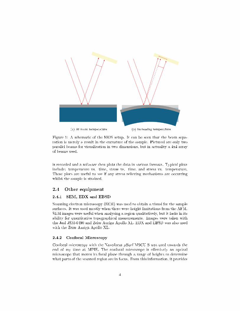
(a) At room temperature (b) Increasing temperature
Figure 1: A schematic of the MOS setup. It can be seen that the beam sepa-ration is merely a result in the curvature of the sample. Pictured are only twoparallel beams for visualization in two dimensions, but in actuality a 4x4 arrayof beams used.
is recorded and a software then plots the data in various formats. Typical plotsinclude: temperature vs. time, stress vs. time, and stress vs. temperature.These plots are useful to see if any stress relieving mechanisms are occurringwhilst the sample is strained.
2.4 Other equipment
2.4.1 SEM, EDX and EBSD
Scanning electron microscopy (SEM) was used to obtain a visual for the samplesurfaces. It was used mostly when there were height limitations from the AFM.SEM images were useful when analysing a region qualitatively, but it lacks in itsability for quantitative topographical measurements. Images were taken withthe Jeol JSM-6490 and Zeiss Auriga Apollo XL. EDX and EBSD was also usedwith the Zeiss Auriga Apollo XL.
2.4.2 Confocal Microscopy
Confocal microscopy with the Nanofocus µSurf MSCU S was used towards theend of my time at MPIE. The confocal microscope is e�ectively an opticalmicroscope that moves its focal plane through a range of heights to determinewhat parts of the scanned region are in focus. From this information, it provides
4

quantitative data for the topography of a sample like AFM, but has no heightlimitations. Consequently the data from this method is utilized for sampleswith a large height di�erence that could not be mapped by AFM. Confocalmicroscopy has its faults: in many high sloping regions, it is unable to registerthe height and leads to many images with areas of missing data.
2.4.3 Gwyddion
Gwyddion is a data processing software. It was used to post-process manyimages and mappings by �attening images and selecting grains by threshold.
5
3 Experimentation, Results and Discusssion
3.1 Nanotribological investigation of plasticity in micro-
scratched copper
The �rst sample to be studied was a thin �lm of Cu. An investigation into themicromechanical properties of Cu is an ideal start due to prior experience in theinstitute with austenite. Cu and austenite are both FCC materials and shouldtherefore relieve stress via dislocation motion in a similar way.
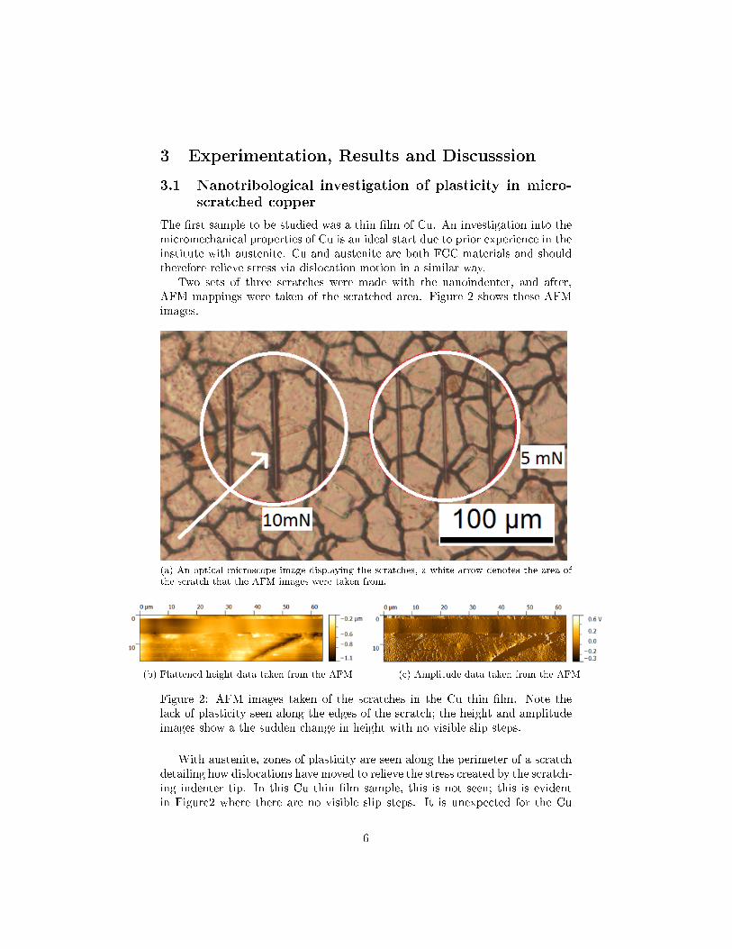
Two sets of three scratches were made with the nanoindenter, and after,AFM mappings were taken of the scratched area. Figure 2 shows these AFMimages.
(a) An optical microscope image displaying the scratches, a white arrow denotes the area ofthe scratch that the AFM images were taken from.
(b) Flattened height data taken from the AFM (c) Amplitude data taken from the AFM
Figure 2: AFM images taken of the scratches in the Cu thin �lm. Note thelack of plasticity seen along the edges of the scratch; the height and amplitudeimages show a the sudden change in height with no visible slip steps.
With austenite, zones of plasticity are seen along the perimeter of a scratchdetailing how dislocations have moved to relieve the stress created by the scratch-ing indenter tip. In this Cu thin �lm sample, this is not seen; this is evidentin Figure2 where there are no visible slip steps. It is unexpected for the Cu
6
indenter radius/µm desired scratch depth/µm→indenter load/ mN
5 2→52 (E) 1→30 (D) 0.5→14 (C) 0.25→5.5 (B) 0.125→1.5 (A)10 4→200 (J) 2→118 (I) 1→61 (H) 0.5→30 (G) 0.25→12 (F)20 n/a 4→450 (N) 2→250 (M) 1→125 (L) 0.5→60 (K)
indenter radius : scratch depth ratio 5 : 2 5 : 1 10 : 1 20 : 1 40 : 1
Table 1: A table detailing what load was used for a given indenter radius anddesired scratch depth. There are only 4 sets of 3 scratches for the 20µm radiusindenter because for a depth of 8µm, the required load would be upwards of600mN, which is the limit of the load sensor on the nanoindenter. The letter inbrackets for each load will be used as a reference for a speci�c scratch.
thin �lm to deform in a way that is extremely di�erent to austenite due to theirshared FCC structure.
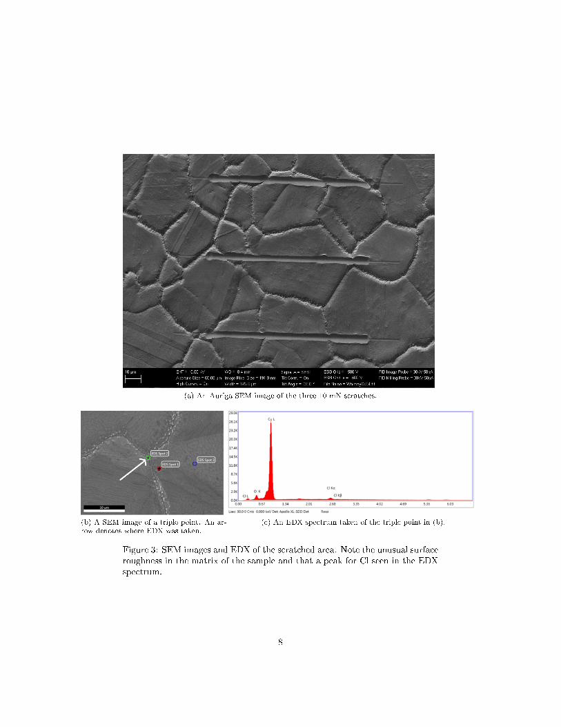
To experiment further, SEM images and EDX were taken; these can be seenin Figure 3.
What was found in the SEM was also unexpected; the roughness of the ma-trix and the apparent Cl precipitates at the grain boundaries and triple pointswere an unknown factor before sample preparation and scratching. Since themicrostructure and purity of the sample was unknown, a nanotribological inves-tigation was not continued; it is di�cult to try and explain stress relief mecha-nisms that are occurring on a sample of unknown composition/microstructure.
The next sample chosen was bulk polycrystaline Cu. This sample was chosennext not only because it was known to be very pure, but also because themechanics of bulk metals are far better known than that of thin �lms. Thesample was cut from a rod of high purity Cu into wedges that were then groundand polished for the purpose of viewing under various microscopy methods.The grain size was measured to be 41µm from the mean line intercept method.Indenting with a Berkovich tip allowed for measurement the sample's Young'smodulus (140 MPa) and hardness (1.5 GPa).
The next goal was to create scratches of a speci�ed depth into the samplewith varying indenter radii. By doing this, we can compare if the indenterradius : scratch depth ratio has any in�uence over how the material deforms.However, when programming scratches, the depth can only be changed with avarying force. So, to know the corresponding depth for each normal force of theindenter, a set of nine indents were made before scratching to obtain this data.From the indenter load against indenter depth curves, an appropriate force wasselected for each desired scratch depth - this is illustrated in Figure 4. Table 1outlines the load selected for the desired scratch depths of each of the indenterradii.
As described in section 2.2, the nanoindenter makes a pre-scan, scratch andpost-scan on the scratch area. Typical data for this can be found in Figure 5. Itcan be seen that the elastic component of the deformation is mostly constant.The plastic component seems to be more complex and is likely to be in�uenced
7
(a) An Auriga SEM image of the three 10 mN scratches.
(b) A SEM image of a triple point. An ar-row denotes where EDX was taken.
(c) An EDX spectrum taken of the triple point in (b).
Figure 3: SEM images and EDX of the scratched area. Note the unusual surfaceroughness in the matrix of the sample and that a peak for Cl seen in the EDXspectrum.
8
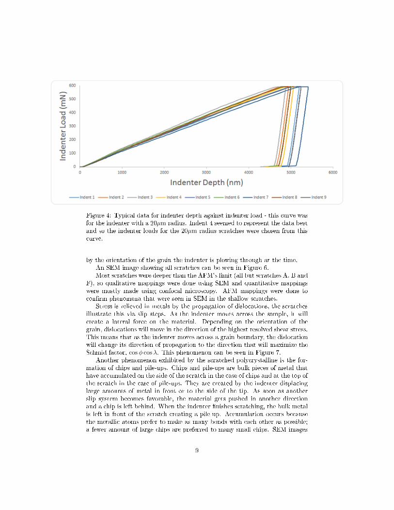
Figure 4: Typical data for indenter depth against indenter load - this curve wasfor the indenter with a 20µm radius. Indent 4 seemed to represent the data bestand so the indenter loads for the 20µm radius scratches were chosen from thiscurve.
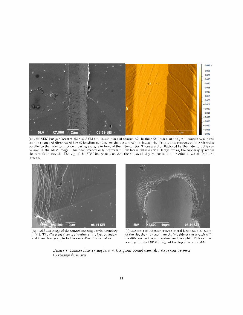
by the orientation of the grain the indenter is plowing through at the time.An SEM image showing all scratches can be seen in Figure 6.Most scratches were deeper than the AFM's limit (all but scratches A, B and
F), so qualitative mappings were done using SEM and quantitative mappingswere mostly made using confocal microscopy. AFM mappings were done tocon�rm phenomena that were seen in SEM in the shallow scratches.
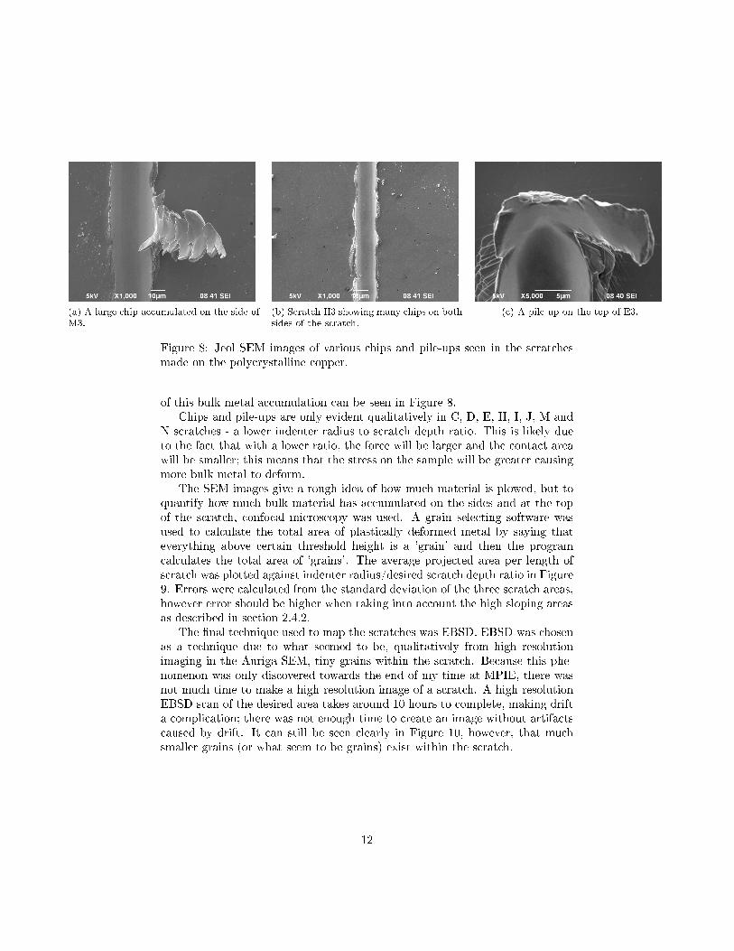
Stress is relieved in metals by the propagation of dislocations, the scratchesillustrate this via slip steps. As the indenter moves across the sample, it willcreate a lateral force on the material. Depending on the orientation of thegrain, dislocations will move in the direction of the highest resolved shear stress.This means that as the indenter moves across a grain boundary, the dislocationwill change its direction of propagation to the direction that will maximize theSchmid factor, cosφ cosλ. This phenomenon can be seen in Figure 7.
Another phenomenon exhibited by the scratched polycrystalline is the for-mation of chips and pile-ups. Chips and pile-ups are bulk pieces of metal thathave accumulated on the side of the scratch in the case of chips and at the top ofthe scratch in the case of pile-ups. They are created by the indenter displacinglarge amounts of metal in front or to the side of the tip. As soon as anotherslip system becomes favorable, the material gets pushed in another directionand a chip is left behind. When the indenter �nishes scratching, the bulk metalis left in front of the scratch creating a pile-up. Accumulation occurs becausethe metallic atoms prefer to make as many bonds with each other as possible;a fewer amount of large chips are preferred to many small chips. SEM images
9
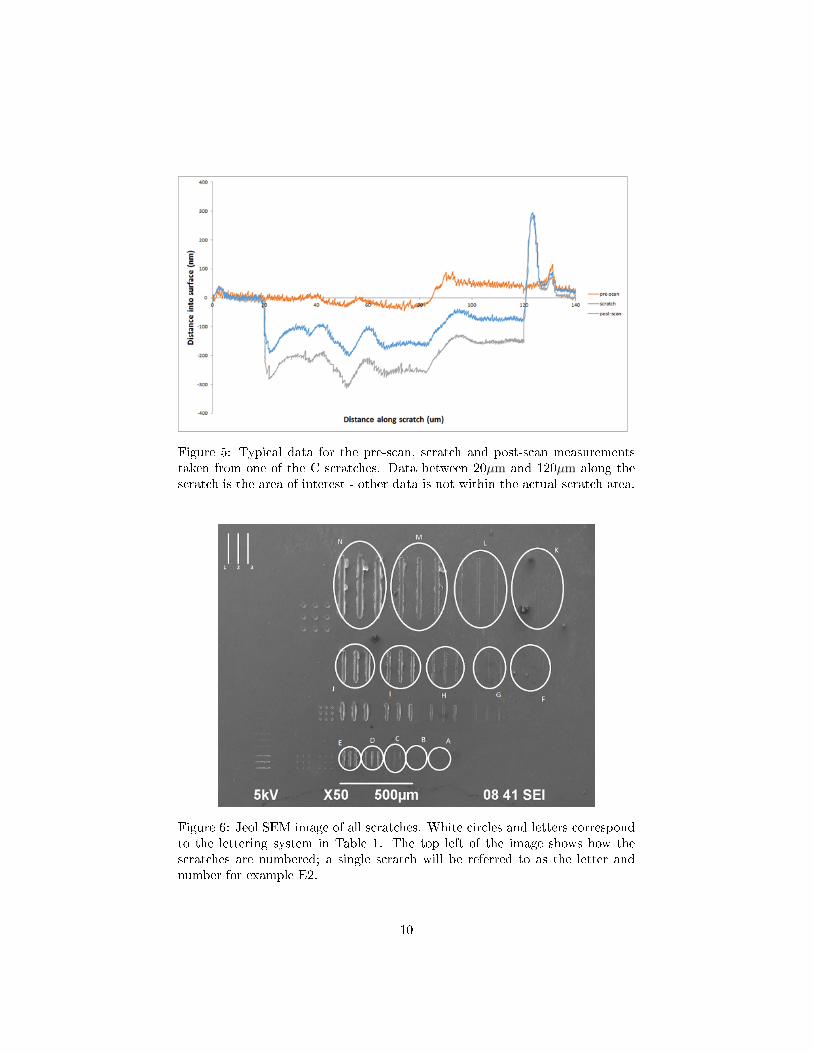
Figure 5: Typical data for the pre-scan, scratch and post-scan measurementstaken from one of the C scratches. Data between 20µm and 120µm along thescratch is the area of interest - other data is not within the actual scratch area.
Figure 6: Jeol SEM image of all scratches. White circles and letters correspondto the lettering system in Table 1. The top left of the image shows how thescratches are numbered; a single scratch will be referred to as the letter andnumber for example E2.
10
(a) Jeol SEM image of scratch B3 and AFM amplitude image of scratch B2. In the SEM image, at the grain boundary, one cansee the change of direction of the dislocation motion. At the bottom of this image, the dislocations propagated in a directionparallel to the indenter motion creating troughs in front of the indenter tip. These are then �attened by the indenter; this canbe seen in the AFM image. This phenomenon only occurs with low forces, whereas with larger forces, the topography withinthe scratch is smooth. The top of the SEM image tells us that the activated slip system is in a direction outwards from thescratch.
(b) Jeol SEM image of the scratch crossing a twin boundaryin M3. The slip steps change direction at the �rst boundaryand then change again to the same direction as before.
(c) Because the indenter creates lateral forces on both sidesof the tip, the slip system on the left side of the scratch willbe di�erent to the slip system on the right. This can beseen by the Jeol SEM image of the top of scratch M3.
Figure 7: Images illustrating how at the grain boundaries, slip steps can be seento change direction.
11
(a) A large chip accumulated on the side ofM3.
(b) Scratch H3 showing many chips on bothsides of the scratch.
(c) A pile-up on the top of E3.
Figure 8: Jeol SEM images of various chips and pile-ups seen in the scratchesmade on the polycrystalline copper.
of this bulk metal accumulation can be seen in Figure 8.Chips and pile-ups are only evident qualitatively in C, D, E, H, I, J, M and
N scratches - a lower indenter radius to scratch depth ratio. This is likely dueto the fact that with a lower ratio, the force will be larger and the contact areawill be smaller; this means that the stress on the sample will be greater causingmore bulk metal to deform.
The SEM images give a rough idea of how much material is plowed, but toquantify how much bulk material has accumulated on the sides and at the topof the scratch, confocal microscopy was used. A grain selecting software wasused to calculate the total area of plastically deformed metal by saying thateverything above certain threshold height is a 'grain' and then the programcalculates the total area of 'grains'. The average projected area per length ofscratch was plotted against indenter radius/desired scratch depth ratio in Figure9. Errors were calculated from the standard deviation of the three scratch areas,however error should be higher when taking into account the high sloping areasas described in section 2.4.2.
The �nal technique used to map the scratches was EBSD. EBSD was chosenas a technique due to what seemed to be, qualitatively from high resolutionimaging in the Auriga SEM, tiny grains within the scratch. Because this phe-nomenon was only discovered towards the end of my time at MPIE, there wasnot much time to make a high resolution image of a scratch. A high resolutionEBSD scan of the desired area takes around 10 hours to complete, making drifta complication; there was not enough time to create an image without artifactscaused by drift. It can still be seen clearly in Figure 10, however, that muchsmaller grains (or what seem to be grains) exist within the scratch.
12
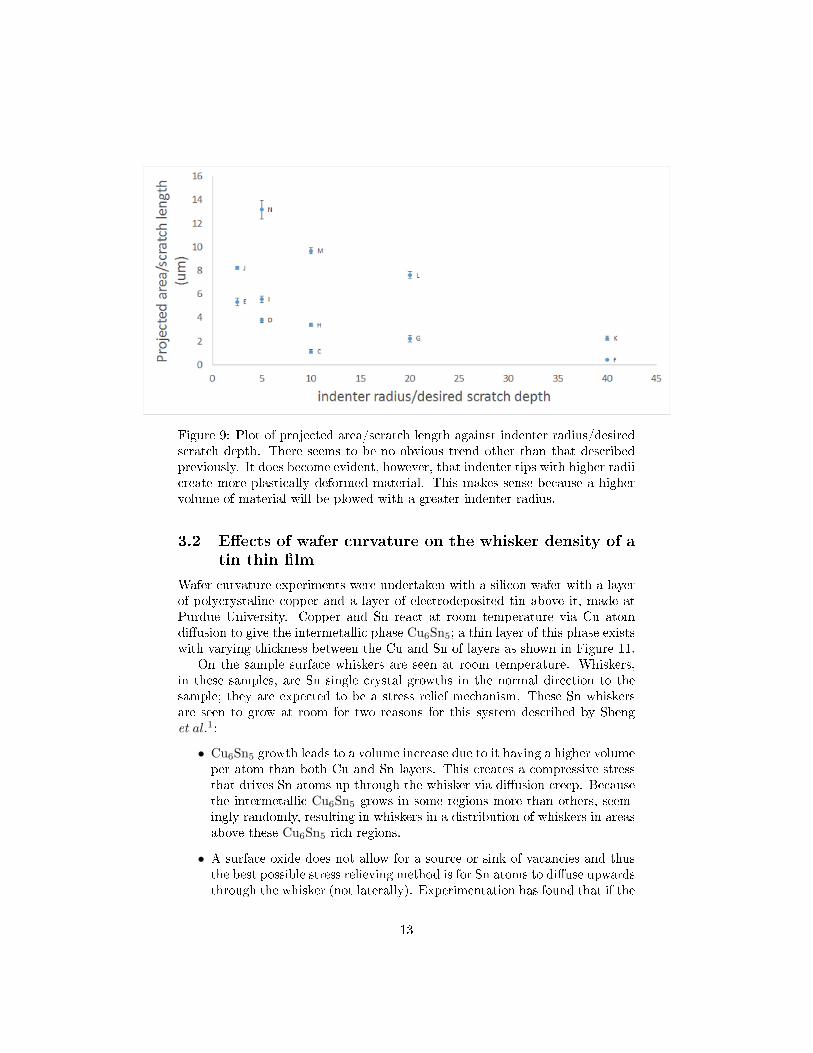
Figure 9: Plot of projected area/scratch length against indenter radius/desiredscratch depth. There seems to be no obvious trend other than that describedpreviously. It does become evident, however, that indenter tips with higher radiicreate more plastically deformed material. This makes sense because a highervolume of material will be plowed with a greater indenter radius.
3.2 E�ects of wafer curvature on the whisker density of a
tin thin �lm
Wafer curvature experiments were undertaken with a silicon wafer with a layerof polycrystaline copper and a layer of electrodeposited tin above it, made atPurdue University. Copper and Sn react at room temperature via Cu atomdi�usion to give the intermetallic phase Cu6Sn5; a thin layer of this phase existswith varying thickness between the Cu and Sn of layers as shown in Figure 11.
On the sample surface whiskers are seen at room temperature. Whiskers,in these samples, are Sn single crystal growths in the normal direction to thesample; they are expected to be a stress relief mechanism. These Sn whiskersare seen to grow at room for two reasons for this system described by Shenget al.1:
• Cu6Sn5 growth leads to a volume increase due to it having a higher volumeper atom than both Cu and Sn layers. This creates a compressive stressthat drives Sn atoms up through the whisker via di�usion creep. Becausethe intermetallic Cu6Sn5 grows in some regions more than others, seem-ingly randomly, resulting in whiskers in a distribution of whiskers in areasabove these Cu6Sn5 rich regions.
• A surface oxide does not allow for a source or sink of vacancies and thusthe best possible stress relieving method is for Sn atoms to di�use upwardsthrough the whisker (not laterally). Experimentation has found that if the
13
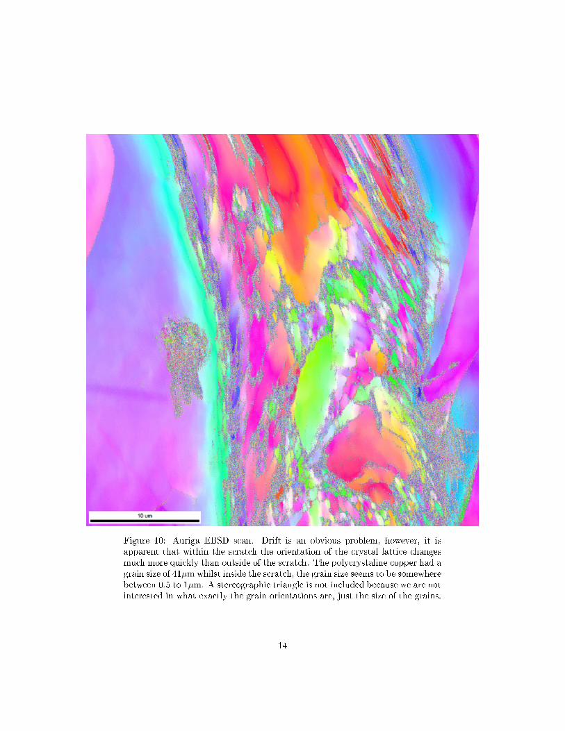
Figure 10: Auriga EBSD scan. Drift is an obvious problem, however, it isapparent that within the scratch the orientation of the crystal lattice changesmuch more quickly than outside of the scratch. The polycrystaline copper had agrain size of 41µm whilst inside the scratch, the grain size seems to be somewherebetween 0.5 to 1µm. A stereographic triangle is not included because we are notinterested in what exactly the grain orientations are, just the size of the grains.
14
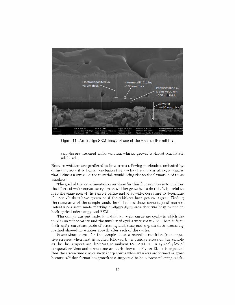
Figure 11: An Auriga SEM image of one of the wafers after milling.
samples are prepared under vacuum, whisker growth is almost completelyinhibited.
Because whiskers are predicted to be a stress relieving mechanism activated bydi�usion creep, it is logical conclusion that cycles of wafer curvature, a processthat induces a stress on the material, would bring rise to the formation of thesewhiskers.
The goal of the experimentation on these Sn thin �lm samples is to monitorthe e�ects of wafer curvature cycles on whisker growth. To do this, it is useful tomap the same area of the sample before and after wafer curvature to determineif more whiskers have grown or if the whiskers have gotten larger. Findingthe same area of the sample would be di�cult without some type of marker.Indentations were made marking a 50µmx50µm area that was easy to �nd inboth optical microscopy and SEM.
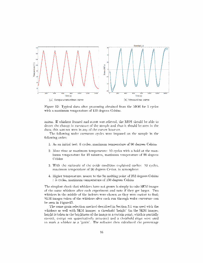
The sample was put under four di�erent wafer curvature cycles in which themaximum temperature and the number of cycles were controlled. Results fromboth wafer curvature plots of stress against time and a grain data processingmethod showed no whisker growth after each of the cycles.
Stress-time curves for the sample show a smooth transition from nega-tive stresses when heat is applied followed by a positive stress on the sampleas the the temperature decreases to ambient temperature. A typical plot oftemperature-time and stress-time are each shown in Figure 12. It is expectedthat the stress-time curves show sharp spikes when whiskers are formed or growbecause whisker formation/growth is a suspected to be a stress-relieving mech-
15
(a) Temperature-time curve (b) Stress-time curve
Figure 12: Typical data after processing obtained from the MOS for 5 cycleswith a maximum temperature of 150 degrees Celsius.
anism. If whiskers formed and stress was relieved, the MOS should be able todetect the change in curvature of the sample and thus it should be seen in thedata; this was not seen in any of the curves however.
The following wafer curvature cycles were imposed on the sample in thefollowing order:
1. As an initial test: 6 cycles, maximum temperature of 90 degrees Celsius
2. More time at maximum temperature: 10 cycles with a hold at the max-imum temperature for 10 minutes, maximum temperature of 90 degreesCelsius
3. With the rationale of the oxide condition explained earlier: 10 cycles,maximum temperature of 90 degrees Cesius, in atmosphere
4. Higher temperature, nearer to the Sn melting point of 232 degrees Celsius: 5 cycles, maximum temperature of 150 degrees Celsius
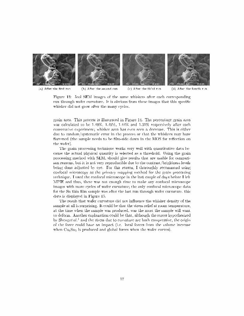
The simplest check that whiskers have not grown is simply to take SEM imagesof the same whiskers after each experiment and note if they get larger. Twowhiskers in the middle of the indents were chosen as they were easiest to �nd;SEM images taken of the whiskers after each run through wafer curvature canbe seen in Figure13.
The same grain selection method described in Section 3.1 was used with thewhiskers as well with SEM images: a threshold 'height' (in the SEM images,height is taken as the brightness of the image at a certain point, which is partiallycorrect, except not quantitatively accurate) and a threshold slope were usedto mark a whisker as a 'grain'. The software then calculated the percentage
16
(a) After the �rst run (b) After the second run (c) After the third run (d) After the fourth run
Figure 13: Jeol SEM images of the same whiskers after each correspondingrun through wafer curvature. It is obvious from these images that this speci�cwhisker did not grow after the many cycles.
grain area. This process is illustrated in Figure 14. The percentage grain areawas calculated to be 1.49%, 1.49%, 1.44% and 1.31% respectively after eachconsecutive experiment; whisker area has even seen a decrease. This is eitherdue to random/systematic error in the process or that the whiskers may have�attened (the sample needs to be �lm-side down in the MOS for re�ection onthe wafer).
The grain processing technique works very well with quantitative data be-cause the actual physical quantity is selected as a threshold. Using the grainprocessing method with SEM, should give results that are usable for compari-son reasons, but it is not very reproducible due to the contrast/brightness levelsbeing done adjusted by eye. For this reason, I thoroughly recommend usingconfocal microscopy as the primary mapping method for the grain processingtechnique. I used the confocal microscope in the last couple of days before I leftMPIE and thus, there was not enough time to make any confocal microscopeimages with more cycles of wafer curvature; the only confocal microscope datafor the Sn thin �lm sample was after the last run through wafer curvature, thisdata is displayed in Figure 15.
The result that wafer curvature did not in�uence the whisker density of thesample at all is surprising. It could be that the stress relief at room temperature,at the time when the sample was produced, was the most the sample will wantto deform. Another explanation could be that, although the stress hypothesizedby Shenget al.1 and the stress due to curvature are both compressive, the originof the force could have an impact (i.e. local forces from the volume increasewhen Cu6Sn5 is produced and global forces when the wafer curves).
17
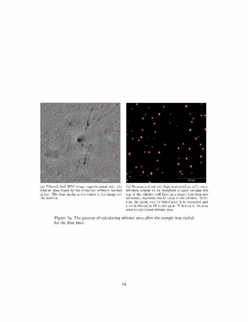
(a) Filtered Jeol SEM image superimposed with thewhisker area found by the threshold software markedin red. The four marks in the center of the image arethe indents.
(b) Because a threshold slope is selected as well, manywhiskers appear to be doughnut shaped because thetop of the whisker will have zero slope; this does notaccurately represent the full area of the whisker. To �xthis, the grain area in Sub-Figure b is extracted andthen is �ltered to �ll in the gaps. This area is the areaused to calculated whisker area
Figure 14: The process of calculating whisker area after the sample was cycledfor the �rst time.
18
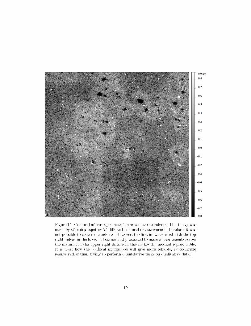
Figure 15: Confocal microscope data of an area near the indents. This image wasmade by stitching together 25 di�erent confocal measurements, therefore, it wasnot possible to center the indents. However, the �rst image started with the topright indent in the lower left corner and proceeded to make measurements acrossthe material in the upper-right direction; this makes the method reproducible.It is clear how the confocal microscope will give more reliable, reproducibleresults rather than trying to perform quantitative tasks on qualitative data.
19
4 Conclusion
One can conclude from the results that polycrystalline copper deforms plasti-cally in a way that visually con�rms, that even at the small scale, plasticity inmetals is dominated my propagation of dislocations. SEM images qualitativelyshow us that dislocations propogate directionally in di�erent grains and on op-posite sides of the indenter tip and that chips and pile-ups form with high forces.Although there does not seem to be a trend that can predict how much mate-rial plastically deforms, it is very clear (logically and with supporting data) thatwith a larger volume of material to be pushed by the indenter as it scratches, alarger amount of material is seen to plastically deform and appear near the edgesof the scratch. Although these results do not answer any questions that wereinitially asked, they could prove to be valuable in the future of nanotribology.If more time were alotted to this nanotribological investigation, high resolutionEBSD mappings of the scratch without drift should be taken and the cause ofhow these seemingly miniature grains formed should be studdied.
Stress-time plots and SEM images, qualitatively and quantitatively, do notshow any growth with cycles through the wafer curvature which is a result withinitself; it was expected for whiskers to be produced when the sample was subjectto stresses. There could be many reasons why whisker growth did not occur andfurther experimentation would be needed to determine the true cause of this.Furthermore, confocal microscopy measurements should be used in the futurefor a more reproducible data-processing technique to monitor whisker growth.
Although no major discovery was achieved during my two months at MPIE,the overall aim of my internship was to gain valuable experience and insight intowhat it is like to work as a researcher of Materials Science. This was certainlyattained. The above �ndings hopefully prove useful in the future at Departmentof Nano-/Micromechanics of Materials.
20

References
A special thank you to Ste�en Brinckmann and Bastian Philippi fortheir dedicated time and insight whilst supervising me during mystay at MPIE. A second thank you to Prof. Dr. Gerhard Dehm forthe opportunity at his wonderful research institute, Department ofNano-/Micromechanics of Materials, at MPIE, Dusseldorf.
1G. Sheng et al. J. Appl. Phys. 92, 64 (2002).
21