micron m25pe80 serial flash memory - rs components · micron m25pe80 serial flash memory serial...
TRANSCRIPT
Micron M25PE80 Serial Flash MemorySerial Flash Memory with Byte Alterability, 75 MHz SPI bus, StandardPinout
Features• 8Mb of page-erasable Flash memory• 2.7V to 3.6V single supply voltage• SPI bus-compatible serial interface• 75 MHz clock rate (maximum)• Page size: 256 bytes
– Page write in 11ms (TYP)– Page program in 0.8ms (TYP)– Page erase in 10ms (TYP)
• Subsector erase: 4KB– Sector erase: 64KB– Bulk erase: 8Mb
• Deep power-down mode: 1µA (TYP)• Electronic signature
– JEDEC standard 2-byte signature (8014h)– Unique ID code (UID) with 16 bytes read-only
• Software write-protection on a 64KB sector basis• Hardware write protection of the memory area se-
lected using the BP0, BP1, and BP2 bits• More than 100,000 write cycles• More than 20 years of data retention• Packages (RoHS compliant)
– VFQFPN8 (MP) 6mm x 5mm (MLP8)– QFN8L (MS) 6mm x 5mm (MLP8)– SO8W (MW) 208 mils– SO8N (MN) 150 mils
• Automotive grade parts available
Micron M25PE80 Serial Flash MemoryFeatures
PDF: 09005aef845660f2m25pe80.pdf - Rev. B 11/12 EN 1 Micron Technology, Inc. reserves the right to change products or specifications without notice.
© 2012 Micron Technology, Inc. All rights reserved.
Products and specifications discussed herein are subject to change by Micron without notice.
ContentsFunctional Description ..................................................................................................................................... 5Signal Descriptions ........................................................................................................................................... 7SPI Modes ........................................................................................................................................................ 8Operating Features ......................................................................................................................................... 10
Sharing the overhead of modifying data ...................................................................................................... 10An easy way to modify data ......................................................................................................................... 10A fast way to modify data ............................................................................................................................ 10Polling during a Write, Program, or Erase Cycle ............................................................................................ 11Reset .......................................................................................................................................................... 11Active Power, Standby Power, and Deep Power-Down .................................................................................. 11Status Register ............................................................................................................................................ 11Protection Modes ....................................................................................................................................... 11Specific Hardware and Software Protection ................................................................................................. 12
Memory Organization .................................................................................................................................... 15Command Set Overview ................................................................................................................................. 18WRITE ENABLE .............................................................................................................................................. 20WRITE DISABLE ............................................................................................................................................. 21READ IDENTIFICATION ................................................................................................................................. 22READ STATUS REGISTER ................................................................................................................................ 23
WIP Bit ...................................................................................................................................................... 23WEL Bit ...................................................................................................................................................... 23Block Protect Bits ....................................................................................................................................... 24SRWD Bit ................................................................................................................................................... 24
WRITE STATUS REGISTER .............................................................................................................................. 25READ DATA BYTES ......................................................................................................................................... 27READ DATA BYTES at HIGHER SPEED ............................................................................................................ 28READ LOCK REGISTER ................................................................................................................................... 29PAGE WRITE .................................................................................................................................................. 31PAGE PROGRAM ............................................................................................................................................ 33WRITE to LOCK REGISTER ............................................................................................................................. 35PAGE ERASE ................................................................................................................................................... 38SUBSECTOR ERASE ....................................................................................................................................... 39SECTOR ERASE .............................................................................................................................................. 40BULK ERASE .................................................................................................................................................. 41DEEP POWER-DOWN ..................................................................................................................................... 42RELEASE from DEEP POWER-DOWN .............................................................................................................. 43Power-Up and Power-Down ............................................................................................................................ 44RESET ............................................................................................................................................................ 46Initial Delivery State ....................................................................................................................................... 46Maximum Ratings and Operating Conditions .................................................................................................. 47DC Parameters ............................................................................................................................................... 48AC Characteristics .......................................................................................................................................... 50Package Information ...................................................................................................................................... 57Device Ordering Information .......................................................................................................................... 60Revision History ............................................................................................................................................. 61
Rev. B – 11/2012 ......................................................................................................................................... 61Rev. A – 09/2012 .......................................................................................................................................... 61
Micron M25PE80 Serial Flash MemoryFeatures
PDF: 09005aef845660f2m25pe80.pdf - Rev. B 11/12 EN 2 Micron Technology, Inc. reserves the right to change products or specifications without notice.
© 2012 Micron Technology, Inc. All rights reserved.
List of FiguresFigure 1: Logic Diagram ................................................................................................................................... 5Figure 2: Pin Connections: VFQFPN, QFN8L, and SO ........................................................................................ 6Figure 3: SPI Modes Supported ........................................................................................................................ 8Figure 4: Bus Master and Memory Devices on the SPI Bus ................................................................................. 9Figure 5: Block Diagram ................................................................................................................................ 17Figure 6: WRITE ENABLE Command Sequence .............................................................................................. 20Figure 7: WRITE DISABLE Command Sequence ............................................................................................. 21Figure 8: READ IDENTIFICATION Command Sequence ................................................................................. 23Figure 9: READ STATUS REGISTER Command Sequence ................................................................................ 23Figure 10: Status Register Format ................................................................................................................... 24Figure 11: WRITE STATUS REGISTER Command Sequence ............................................................................. 25Figure 12: READ DATA BYTES Command Sequence ........................................................................................ 27Figure 13: READ DATA BYTES at HIGHER SPEED Command Sequence ........................................................... 28Figure 14: READ LOCK REGISTER Command Sequence ................................................................................. 29Figure 15: PAGE WRITE Command Sequence ................................................................................................. 32Figure 16: PAGE PROGRAM Command Sequence ........................................................................................... 34Figure 17: WRITE to LOCK REGISTER Instruction Sequence ........................................................................... 35Figure 18: PAGE ERASE Command Sequence ................................................................................................. 38Figure 19: SUBSECTOR ERASE Command Sequence ...................................................................................... 39Figure 20: SECTOR ERASE Command Sequence ............................................................................................. 40Figure 21: BULK ERASE Command Sequence ................................................................................................. 41Figure 22: DEEP POWER-DOWN Command Sequence ................................................................................... 42Figure 23: RELEASE from DEEP POWER-DOWN Command Sequence ............................................................. 43Figure 24: Power-Up Timing .......................................................................................................................... 45Figure 25: AC Measurement I/O Waveform ..................................................................................................... 50Figure 26: Serial Input Timing ........................................................................................................................ 54Figure 27: Write Protect Setup and Hold Timing ............................................................................................. 54Figure 28: Output Timing .............................................................................................................................. 55Figure 29: Reset AC Waveforms ...................................................................................................................... 56Figure 30: VFQFPN8 (MLP8) 6mm x 5mm ...................................................................................................... 57Figure 31: QFN8L (MLP8) 8-lead, quad flat package no lead, 6mm x 5mm ....................................................... 58Figure 32: SO8W – 8 lead plastic small outline, 208 mils body width ................................................................. 59
Micron M25PE80 Serial Flash MemoryFeatures
PDF: 09005aef845660f2m25pe80.pdf - Rev. B 11/12 EN 3 Micron Technology, Inc. reserves the right to change products or specifications without notice.
© 2012 Micron Technology, Inc. All rights reserved.
List of TablesTable 1: Signal Names ...................................................................................................................................... 6Table 2: Signal Descriptions ............................................................................................................................. 7Table 3: Software Protection Truth Table, 64KB granularity (sectors 0-15) ........................................................ 13Table 4: Not for new design: TY7 process only, software protection scheme truth table (sectors 0 and 15) .......... 13Table 5: Protected Area Sizes .......................................................................................................................... 14Table 6: Memory Organization ....................................................................................................................... 15Table 7: Command Set Codes ........................................................................................................................ 19Table 8: READ IDENTIFICATION Data Out Sequence ..................................................................................... 22Table 9: Status Register Protection Modes ...................................................................................................... 26Table 10: Lock Register Out ............................................................................................................................ 29Table 11: Not for new design: Lock Registers for the M25PE80 in T7Y Process ................................................... 29Table 12: Lock Register In .............................................................................................................................. 35Table 13: Not for new design: lock registers for the M25PE80 in T7Y process .................................................... 35Table 14: Power-up Timing and VWI Threshold ............................................................................................... 45Table 15: Device Status After a RESET# LOW Pulse .......................................................................................... 46Table 16: Absolute Maximum Ratings ............................................................................................................. 47Table 17: Operating Conditions ...................................................................................................................... 47Table 18: DC Characteristics .......................................................................................................................... 48Table 19: DC Characteristics 75 MHz Operation ............................................................................................. 48Table 20: AC Measurement Conditions ........................................................................................................... 50Table 21: Capacitance .................................................................................................................................... 50Table 22: AC Characteristics ........................................................................................................................... 51Table 23: AC Characteristics (50MHz operation) ............................................................................................. 52Table 24: AC Specifications (75 MHz operation) .............................................................................................. 53Table 25: Reset Conditions ............................................................................................................................. 55Table 26: Timings After a RESET# LOW Pulse .................................................................................................. 55Table 27: Standard Part Number Information Scheme ..................................................................................... 60Table 28: Automotive Part Number Information Scheme ................................................................................. 60
Micron M25PE80 Serial Flash MemoryFeatures
PDF: 09005aef845660f2m25pe80.pdf - Rev. B 11/12 EN 4 Micron Technology, Inc. reserves the right to change products or specifications without notice.
© 2012 Micron Technology, Inc. All rights reserved.
Functional DescriptionThe M25PE80 is an 8Mb (1Mb x 8 bit) serial-paged Flash memory device accessed by ahigh-speed SPI-compatible bus.
The memory can be written or programmed 1 to 256 bytes at a time using the PAGEWRITE or PAGE PROGRAM command. The PAGE WRITE command consists of an inte-grated PAGE ERASE cycle followed by a PAGE PROGRAM cycle.
The memory is organized as 16 sectors, divided into 16 subsectors each (256 subsectorstotal). Each sector contains 256 pages and each subsector contains 16 pages. Each pageis 256 bytes wide. The entire memory can be viewed as consisting of 4096 pages, or1,048,576 bytes.
The memory can be erased one page at a time using the PAGE ERASE command, onesector at a time using the SECTOR ERASE command, one subsector at a time using theSUBSECTOR ERASE command, or as a whoe using the BULK ERASE command.
The memory can be write-protected by either hardware or software using a mix of vola-tile and non-volatile protection features, depending on application needs. The protec-tion granularity is 64Kb (sector granularity). The entire memory array is partitioned into4Kb subsectors.
Note: The write protection (defined by the WL and LD lock bits) of the 4KB subsectorsin the top and bottom sectors is no longer offered. For more details, seePCNMPG062148.
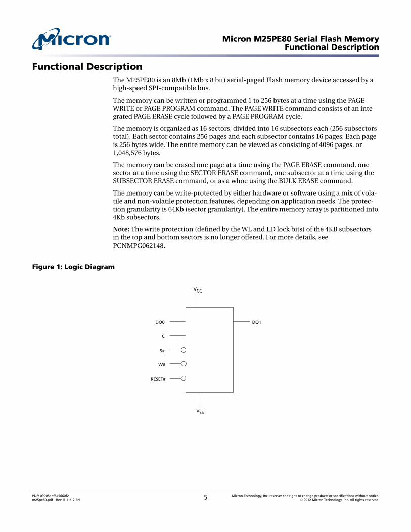
Figure 1: Logic Diagram
S#
VCC
RESET#
VSS
DQ1
C
DQ0
W#
Micron M25PE80 Serial Flash MemoryFunctional Description
PDF: 09005aef845660f2m25pe80.pdf - Rev. B 11/12 EN 5 Micron Technology, Inc. reserves the right to change products or specifications without notice.
© 2012 Micron Technology, Inc. All rights reserved.
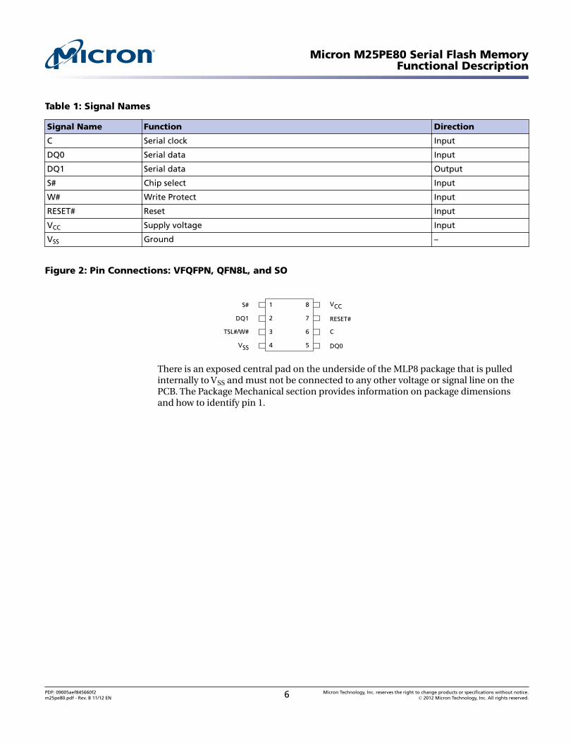
Table 1: Signal Names
Signal Name Function Direction
C Serial clock Input
DQ0 Serial data Input
DQ1 Serial data Output
S# Chip select Input
W# Write Protect Input
RESET# Reset Input
VCC Supply voltage Input
VSS Ground –
Figure 2: Pin Connections: VFQFPN, QFN8L, and SO
1
2
3
4
VCC
RESET#
5
6
7
8
DQ1
VSS
S#
DQ0
C TSL#/W#
There is an exposed central pad on the underside of the MLP8 package that is pulledinternally to VSS and must not be connected to any other voltage or signal line on thePCB. The Package Mechanical section provides information on package dimensionsand how to identify pin 1.
Micron M25PE80 Serial Flash MemoryFunctional Description
PDF: 09005aef845660f2m25pe80.pdf - Rev. B 11/12 EN 6 Micron Technology, Inc. reserves the right to change products or specifications without notice.
© 2012 Micron Technology, Inc. All rights reserved.
Signal Descriptions
Table 2: Signal Descriptions
Signal Type Description
DQ1 Output Serial data: The DQ1 output signal is used to transfer data serially out of the device.Data is shifted out on the falling edge of the serial clock (C).
DQ0 Input Serial data: The DQ0 input signal is used to transfer data serially into the device. Itreceives commands, addresses, and the data to be programmed. Values are latched onthe rising edge of the serial clock (C).
C Input Clock: The C input signal provides the timing of the serial interface. Commands, ad-dresses, or data present at serial data input (DQ0) is latched on the rising edge of theserial clock (C). Data on DQ1 changes after the falling edge of C.
S# Input Chip select: When the S# input signal is HIGH, the device is deselected and DQ1 is atHIGH impedance. Unless an internal READ, PROGRAM, ERASE, or WRITE cycle is in pro-gress, the device will be in the standby power mode (not the DEEP POWER-DOWNmode). Driving S# LOW enables the device, placing it in the active power mode. Afterpower-up, a falling edge on S# is required prior to the start of any command.
RESET# Input Reset: The RESET# input provides a hardware reset for the memory.When RESET# is driven HIGH, the memory is in the normal operating mode. When RE-SET# is driven LOW, the memory will enter the Reset mode. In this mode, the output isat HIGH impedance.Driving RESET# LOW while an internal operation is in progress affects the WRITE, PRO-GRAM, or ERASE cycle, and data may be lost.
W# Input Write protect: The W# input signal is used to freeze the size of the area of memorythat is protected against WRITE, PROGRAM, and ERASE commands as specified by thevalues in the block protect bits in the status register.
VCC Input Supply voltage
VSS Input Ground: Reference for the VCC supply voltage.
Micron M25PE80 Serial Flash MemorySignal Descriptions
PDF: 09005aef845660f2m25pe80.pdf - Rev. B 11/12 EN 7 Micron Technology, Inc. reserves the right to change products or specifications without notice.
© 2012 Micron Technology, Inc. All rights reserved.
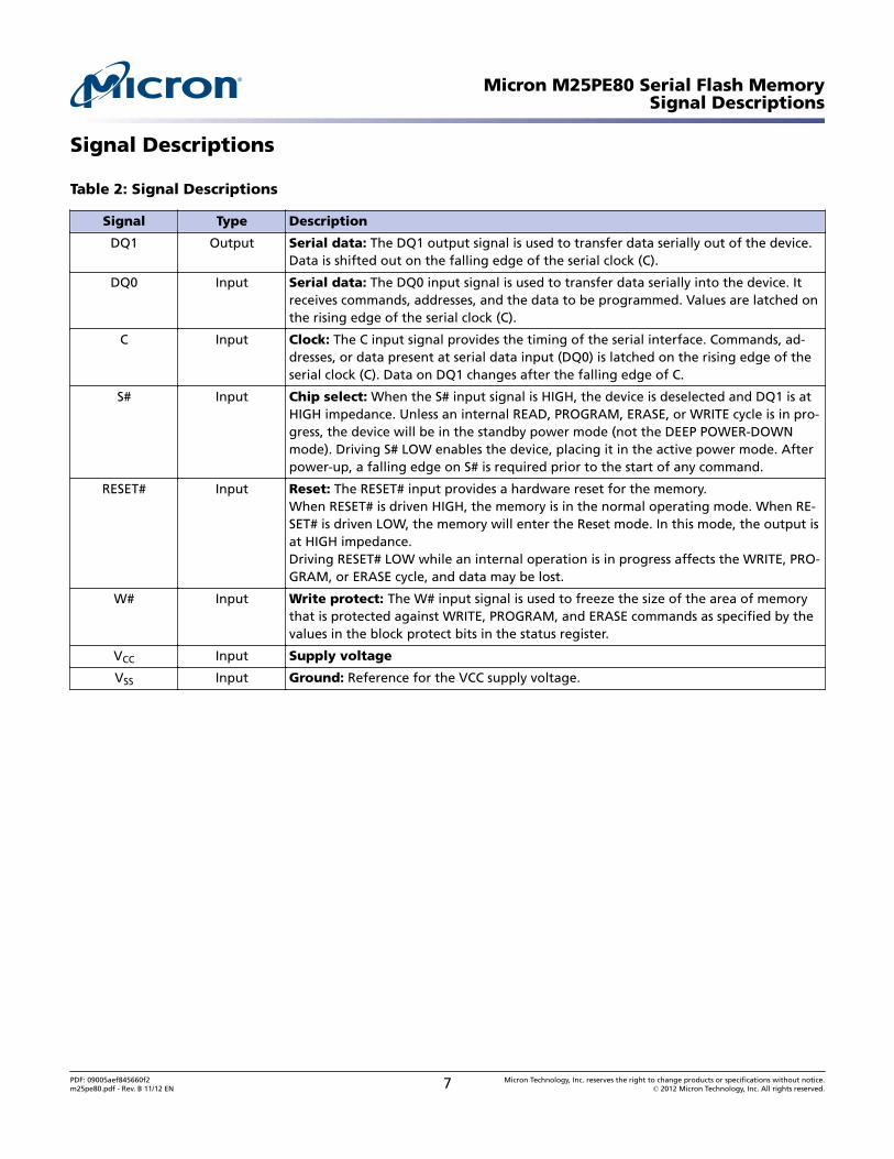
SPI ModesThese devices can be driven by a microcontroller with its serial peripheral interface(SPI) running in either of the following two SPI modes:
• CPOL=0, CPHA=0• CPOL=1, CPHA=1
For these two modes, input data is latched in on the rising edge of serial clock (C), andoutput data is available from the falling edge of C.
The difference between the two modes is the clock polarity when the bus master is inSTANDBY mode and not transferring data:
• C remains at 0 for (CPOL=0, CPHA=0)• C remains at 1 for (CPOL=1, CPHA=1)
Figure 3: SPI Modes Supported
C
MSB
CPHA
DQ0
0
1
CPOL
0
1
DQ1
C
MSB
Because only one device is selected at a time, only one device drives the serial data out-put (DQ1) line at a time, while the other devices are HIGH-Z. An example of three devi-ces connected to an MCU on an SPI bus is shown here.
Micron M25PE80 Serial Flash MemorySPI Modes
PDF: 09005aef845660f2m25pe80.pdf - Rev. B 11/12 EN 8 Micron Technology, Inc. reserves the right to change products or specifications without notice.
© 2012 Micron Technology, Inc. All rights reserved.
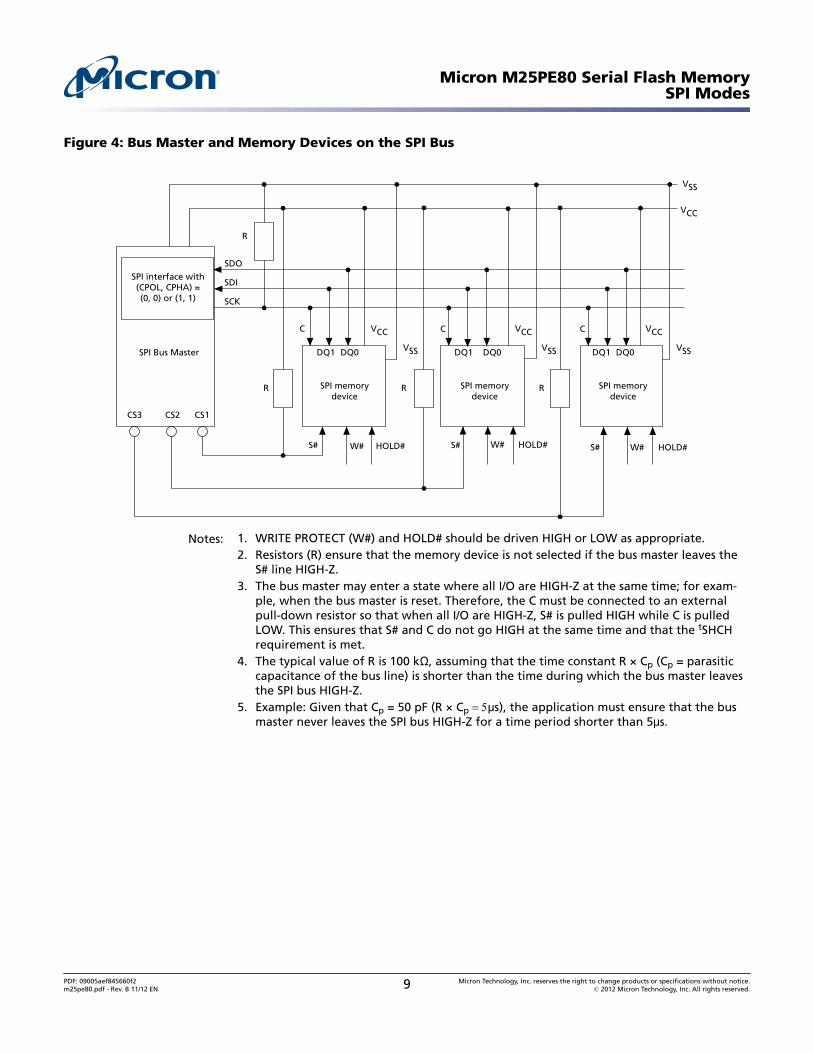
Figure 4: Bus Master and Memory Devices on the SPI Bus
SPI Bus Master
SPI memorydevice
SDO
SDI
SCK
C
DQ1 DQ0
S#
SPI memorydevice
C
DQ1 DQ0
S#
SPI memorydevice
C
DQ1 DQ0
S#
CS3 CS2 CS1
SPI interface with(CPOL, CPHA) =(0, 0) or (1, 1)
W# HOLD# HOLD# W# HOLD#
R R R
VCC
VCC VCC VCC
VSS
VSS VSS VSS
R
W#
Notes: 1. WRITE PROTECT (W#) and HOLD# should be driven HIGH or LOW as appropriate.2. Resistors (R) ensure that the memory device is not selected if the bus master leaves the
S# line HIGH-Z.3. The bus master may enter a state where all I/O are HIGH-Z at the same time; for exam-
ple, when the bus master is reset. Therefore, the C must be connected to an externalpull-down resistor so that when all I/O are HIGH-Z, S# is pulled HIGH while C is pulledLOW. This ensures that S# and C do not go HIGH at the same time and that the tSHCHrequirement is met.
4. The typical value of R is 100 kΩ, assuming that the time constant R × Cp (Cp = parasiticcapacitance of the bus line) is shorter than the time during which the bus master leavesthe SPI bus HIGH-Z.
5. Example: Given that Cp = 50 pF (R × Cp = 5μs), the application must ensure that the busmaster never leaves the SPI bus HIGH-Z for a time period shorter than 5μs.
Micron M25PE80 Serial Flash MemorySPI Modes
PDF: 09005aef845660f2m25pe80.pdf - Rev. B 11/12 EN 9 Micron Technology, Inc. reserves the right to change products or specifications without notice.
© 2012 Micron Technology, Inc. All rights reserved.
Operating Features
Sharing the overhead of modifying data
To write or program one or more data bytes, two commands are required: WRITE ENA-BLE (WREN), which is one byte, and a PAGE WRITE (PW) or PAGE PROGRAM (PP) se-quence, which consists of four bytes plus data. This is followed by the internal cycle ofduration tPW or tPP.
To share this overhead, the PW or PP command allows up to 256 bytes to be program-med (changing bits from 1 to 0) or written (changing bits to 0 or 1) at a time, providedthat they lie in consecutive addresses on the same page of memory.
An easy way to modify data
The Page Write (PW) instruction provides a convenient way of modifying data (up to256 contiguous bytes at a time), and simply requires the start address, and the new datain the instruction sequence.
The Page Write (PW) instruction is entered by driving Chip Select (S#) LOW, and thentransmitting the instruction byte, three address bytes (A23-A0) and at least one databyte, and then driving S# HIGH. While S# is being held LOW, the data bytes are writtento the data buffer, starting at the address given in the third address byte (A7-A0). WhenChip S# is driven HIGH, the Write cycle starts. The remaining unchanged bytes of thedata buffer are automatically loaded with the values of the corresponding bytes of theaddressed memory page. The addressed memory page is then automatically put into anErase cycle. Finally, the addressed memory page is programmed with the contents ofthe data buffer.
All of this buffer management is handled internally, and is transparent to the user. Theuser is given the facility of being able to alter the contents of the memory on a byte-by-byte basis. For optimized timings, it is recommended to use the PAGE WRITE (PW) in-struction to write all consecutive targeted bytes in a single sequence versus using sever-al PAGE WRITE (PW) sequences with each containing only a few bytes.
A fast way to modify data
The PAGE PROGRAM (PP) command providesa fast way of modifying data (up to 256contiguous bytes at a time), provided that it only involves resetting bits to 0 that hadpreviously been set to 1.
This might be:
• When the designer is programming the device for the first time.• When the designer knows that the page has already been erased by an earlier PAGE
ERASE (PE), SUBSECTOR ERASE (SSE), SECTOR ERASE (SE), or BULK ERASE (BE)command. This is useful, for example, when storing a fast stream of data, having firstperformed the erase cycle when time was available.
• When the designer knows that the only changes involve resetting bits to 0 that are stillset to 1. When this method is possible, it has the additional advantage of minimizingthe number of unnecessary erase operations, and the extra stress incurred by eachpage.
Micron M25PE80 Serial Flash MemoryOperating Features
PDF: 09005aef845660f2m25pe80.pdf - Rev. B 11/12 EN 10 Micron Technology, Inc. reserves the right to change products or specifications without notice.
© 2012 Micron Technology, Inc. All rights reserved.
For optimized timings, it is recommended to use the PAGE PROGRAM (PP) instructionto program all consecutive targeted bytes in a single sequence versus using severalPAGE PROGRAM (PP) sequences with each containing only a few bytes.
Polling during a Write, Program, or Erase Cycle
An improvement in the time to complete the following commands can be achieved bynot waiting for the worst case delay (tPW, tPP, tPE, tBE, tWor tSE).
The write in progress (WIP) bit is provided in the status register so that the applicationprogram can monitor this bit in the status register, polling it to establish when the pre-vious WRITE cycle, PROGRAM cycle, or ERASE cycle is complete.
Reset
An internal power-on reset circuit helps protect against inadvertent data writes. Addi-tional protection is provided by driving RESET# LOW during the power-on process, andonly driving it HIGH when VCC has reached the correct voltage level, VCC(min).
Active Power, Standby Power, and Deep Power-Down
When chip select (S#) is LOW, the device is selected and in the ACTIVE POWER mode.
When S# is HIGH, the device is deselected, but could remain in the ACTIVE POWERmode until all internal cycles have completed (PROGRAM, ERASE, WRITE). The devicethen goes in to the STANDBY POWER mode. The device consumption drops to ICC1.
The DEEP POWER-DOWN mode is entered when the DEEP POWER-DOWN commandis executed. The device consumption drops further to ICC2. The device remains in thismode until the RELEASE FROM DEEP POWER-DOWN command is executed. While inthe DEEP POWER-DOWN mode, the device ignores all WRITE, PROGRAM, and ERASEcommands. This provides an extra software protection mechanism when the device isnot in active use, by protecting the device from inadvertent WRITE, PROGRAM, orERASE operations.
Status Register
The status register contains a number of status bits that can be read by the READ STA-TUS REGISTER (RDSR) command.
Protection Modes
Non-volatile memory is used in environments that can include excessive noise. The fol-lowing capabilities help protect data in these noisy environments.
Power on reset and an internal timer (tPUW) can provide protection against inadvertentchanges while the power supply is outside the operating specification.
WRITE, PROGRAM, and ERASE commands are checked before they are accepted for ex-ecution to ensure they consist of a number of clock pulses that is a multiple of eight.
All commands that modify data must be preceded by a WRITE ENABLE command to setthe write enable latch (WEL) bit. This bit is returned to its reset state by the followingevents.
• Power-up• Reset (RESET#) driven LOW
Micron M25PE80 Serial Flash MemoryOperating Features
PDF: 09005aef845660f2m25pe80.pdf - Rev. B 11/12 EN 11 Micron Technology, Inc. reserves the right to change products or specifications without notice.
© 2012 Micron Technology, Inc. All rights reserved.
• WRITE DISABLE (WRDI) command completion• PAGE WRITE (PW) command completion• PAGE PROGRAM (PP) command completion• WRITE TO LOCK REGISTER (WRLR) command completion• PAGE ERASE (PE) command completion• SUBSECTOR ERASE (SSE) command completion• SECTOR EASE (SE) command completion• BULK ERASE (BE) command completion
The Reset (RESET#) signal can be driven LOW to freeze and reset the internal logic.
In addition to the low power consumption feature, DEEP POWER-DOWN mode offersextra software protection from inadvertant WRITE, PROGRAM, and ERASE commandswhile the device is not in active use.
Specific Hardware and Software Protection
The M25PE80 features a hardware protected mode (HPM) and two software protectedmodes (SPM1 and SPM2). SPM1 and SPM2 can be combined to protect the memory ar-ray as required.
Hardware Protected Mode (HPM)
The Hardware Protected Mode (HPM) is used to write-protect the non-volatile bits ofthe Status Register (that is, the Block Protect Bits and the Status Register bit). HPM isentered by driving the Write Protect (W#) signal LOW with the SRWD bit set to HIGH.This additional protection allows the Status Register to be hardware-protected.
SPM1 and SPM2
The first Software Protected Mode (SPM1) is managed by specific Lock Registers as-signed to each 64KB sector.
The Lock Registers can be read and written using the Read Lock Register (RDLR) andWrite to Lock Register (WRLR) commands.
In each Lock Register, two bits control the protection of each sector: the Write Lock bitand the Lock Down bit.
• Write lock bit: This bit determines whether the contents of the sector can be modifiedusing the WRITE, PROGRAM, and ERASE commands. When the bit is set to ‘1’, thesector is write protected, and any operations that attempt to change the data in thesector will fail. When the bit is reset to ‘0’, the sector is not write protected by the lockregister, and may be modified.
• Lock down bit: This bit provides a mechanism for protecting software data from sim-ple hacking and malicious attack. When the bit is set to '1’, further modification to thewrite lock bit and lock down bit cannot be performed. A power-up, is required beforechanges to these bits can be made. When the bit is reset to ‘0’, the write lock bit andlock down bit can be changed.
The Write Lock bit and the Lock Down bit are volatile and their value is reset to 0 after apower-down or reset.
The software protection truth table shows the lock down bit and write lock bit settingsand the sector protection status.
Micron M25PE80 Serial Flash MemoryOperating Features
PDF: 09005aef845660f2m25pe80.pdf - Rev. B 11/12 EN 12 Micron Technology, Inc. reserves the right to change products or specifications without notice.
© 2012 Micron Technology, Inc. All rights reserved.
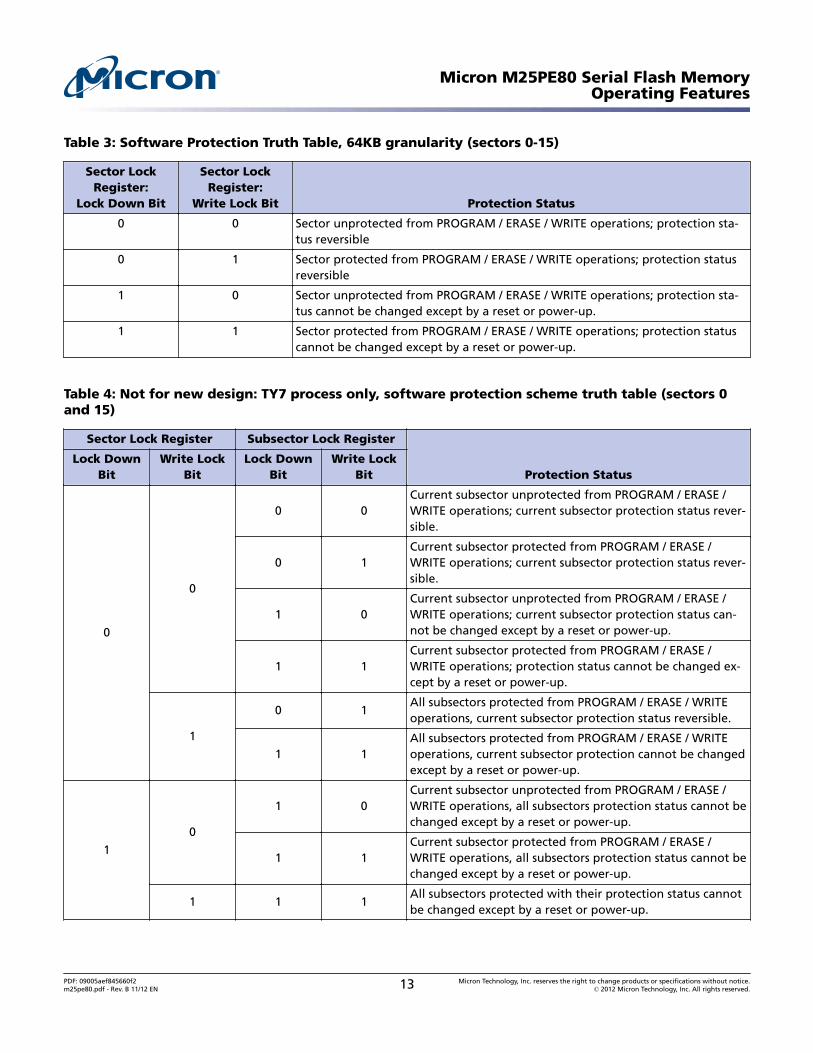
Table 3: Software Protection Truth Table, 64KB granularity (sectors 0-15)
Sector LockRegister:
Lock Down Bit
Sector LockRegister:
Write Lock Bit Protection Status
0 0 Sector unprotected from PROGRAM / ERASE / WRITE operations; protection sta-tus reversible
0 1 Sector protected from PROGRAM / ERASE / WRITE operations; protection statusreversible
1 0 Sector unprotected from PROGRAM / ERASE / WRITE operations; protection sta-tus cannot be changed except by a reset or power-up.
1 1 Sector protected from PROGRAM / ERASE / WRITE operations; protection statuscannot be changed except by a reset or power-up.
Table 4: Not for new design: TY7 process only, software protection scheme truth table (sectors 0and 15)
Sector Lock Register Subsector Lock Register
Protection StatusLock Down
BitWrite Lock
BitLock Down
BitWrite Lock
Bit
0
0
0 0Current subsector unprotected from PROGRAM / ERASE /WRITE operations; current subsector protection status rever-sible.
0 1Current subsector protected from PROGRAM / ERASE /WRITE operations; current subsector protection status rever-sible.
1 0Current subsector unprotected from PROGRAM / ERASE /WRITE operations; current subsector protection status can-not be changed except by a reset or power-up.
1 1Current subsector protected from PROGRAM / ERASE /WRITE operations; protection status cannot be changed ex-cept by a reset or power-up.
1
0 1All subsectors protected from PROGRAM / ERASE / WRITEoperations, current subsector protection status reversible.
1 1All subsectors protected from PROGRAM / ERASE / WRITEoperations, current subsector protection cannot be changedexcept by a reset or power-up.
1
0
1 0Current subsector unprotected from PROGRAM / ERASE /WRITE operations, all subsectors protection status cannot bechanged except by a reset or power-up.
1 1Current subsector protected from PROGRAM / ERASE /WRITE operations, all subsectors protection status cannot bechanged except by a reset or power-up.
1 1 1All subsectors protected with their protection status cannotbe changed except by a reset or power-up.
Micron M25PE80 Serial Flash MemoryOperating Features
PDF: 09005aef845660f2m25pe80.pdf - Rev. B 11/12 EN 13 Micron Technology, Inc. reserves the right to change products or specifications without notice.
© 2012 Micron Technology, Inc. All rights reserved.
All other bit combinations are not-applicable. For more details, see the WRLR instruc-tion.
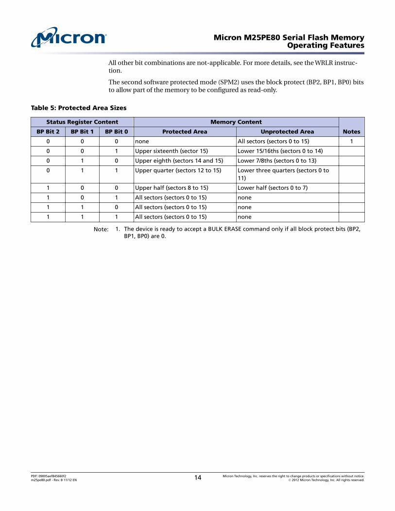
The second software protected mode (SPM2) uses the block protect (BP2, BP1, BP0) bitsto allow part of the memory to be configured as read-only.
Table 5: Protected Area Sizes
Status Register Content Memory Content
NotesBP Bit 2 BP Bit 1 BP Bit 0 Protected Area Unprotected Area
0 0 0 none All sectors (sectors 0 to 15) 1
0 0 1 Upper sixteenth (sector 15) Lower 15/16ths (sectors 0 to 14)
0 1 0 Upper eighth (sectors 14 and 15) Lower 7/8ths (sectors 0 to 13)
0 1 1 Upper quarter (sectors 12 to 15) Lower three quarters (sectors 0 to11)
1 0 0 Upper half (sectors 8 to 15) Lower half (sectors 0 to 7)
1 0 1 All sectors (sectors 0 to 15) none
1 1 0 All sectors (sectors 0 to 15) none
1 1 1 All sectors (sectors 0 to 15) none
Note: 1. The device is ready to accept a BULK ERASE command only if all block protect bits (BP2,BP1, BP0) are 0.
Micron M25PE80 Serial Flash MemoryOperating Features
PDF: 09005aef845660f2m25pe80.pdf - Rev. B 11/12 EN 14 Micron Technology, Inc. reserves the right to change products or specifications without notice.
© 2012 Micron Technology, Inc. All rights reserved.
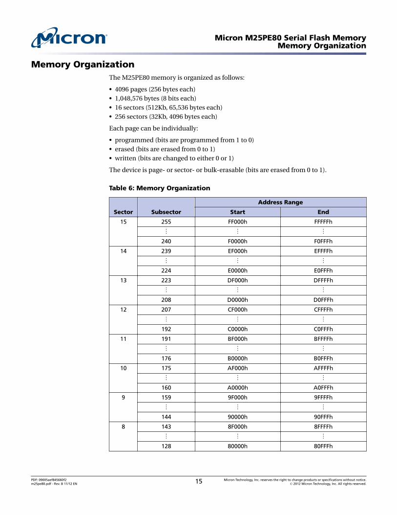
Memory OrganizationThe M25PE80 memory is organized as follows:
• 4096 pages (256 bytes each)• 1,048,576 bytes (8 bits each)• 16 sectors (512Kb, 65,536 bytes each)• 256 sectors (32Kb, 4096 bytes each)
Each page can be individually:
• programmed (bits are programmed from 1 to 0)• erased (bits are erased from 0 to 1)• written (bits are changed to either 0 or 1)
The device is page- or sector- or bulk-erasable (bits are erased from 0 to 1).
Table 6: Memory Organization
Sector Subsector
Address Range
Start End
15 255 FF000h FFFFFh
⋮ ⋮ ⋮240 F0000h F0FFFh
14 239 EF000h EFFFFh
⋮ ⋮ ⋮224 E0000h E0FFFh
13 223 DF000h DFFFFh
⋮ ⋮ ⋮208 D0000h D0FFFh
12 207 CF000h CFFFFh
⋮ ⋮ ⋮192 C0000h C0FFFh
11 191 BF000h BFFFFh
⋮ ⋮ ⋮176 B0000h B0FFFh
10 175 AF000h AFFFFh
⋮ ⋮ ⋮160 A0000h A0FFFh
9 159 9F000h 9FFFFh
⋮ ⋮ ⋮144 90000h 90FFFh
8 143 8F000h 8FFFFh
⋮ ⋮ ⋮128 80000h 80FFFh
Micron M25PE80 Serial Flash MemoryMemory Organization
PDF: 09005aef845660f2m25pe80.pdf - Rev. B 11/12 EN 15 Micron Technology, Inc. reserves the right to change products or specifications without notice.
© 2012 Micron Technology, Inc. All rights reserved.
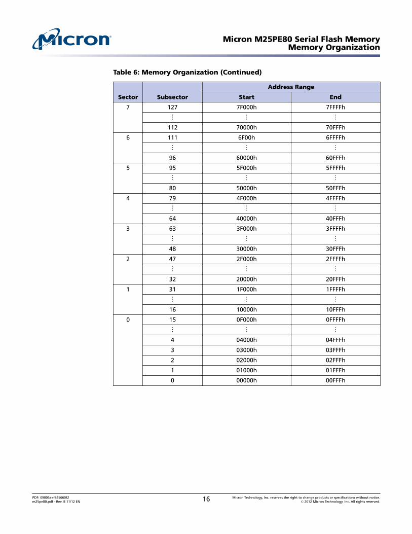
Table 6: Memory Organization (Continued)
Sector Subsector
Address Range
Start End
7 127 7F000h 7FFFFh
⋮ ⋮ ⋮112 70000h 70FFFh
6 111 6F00h 6FFFFh
⋮ ⋮ ⋮96 60000h 60FFFh
5 95 5F000h 5FFFFh
⋮ ⋮ ⋮80 50000h 50FFFh
4 79 4F000h 4FFFFh
⋮ ⋮ ⋮64 40000h 40FFFh
3 63 3F000h 3FFFFh
⋮ ⋮ ⋮48 30000h 30FFFh
2 47 2F000h 2FFFFh
⋮ ⋮ ⋮32 20000h 20FFFh
1 31 1F000h 1FFFFh
⋮ ⋮ ⋮16 10000h 10FFFh
0 15 0F000h 0FFFFh
⋮ ⋮ ⋮4 04000h 04FFFh
3 03000h 03FFFh
2 02000h 02FFFh
1 01000h 01FFFh
0 00000h 00FFFh
Micron M25PE80 Serial Flash MemoryMemory Organization
PDF: 09005aef845660f2m25pe80.pdf - Rev. B 11/12 EN 16 Micron Technology, Inc. reserves the right to change products or specifications without notice.
© 2012 Micron Technology, Inc. All rights reserved.
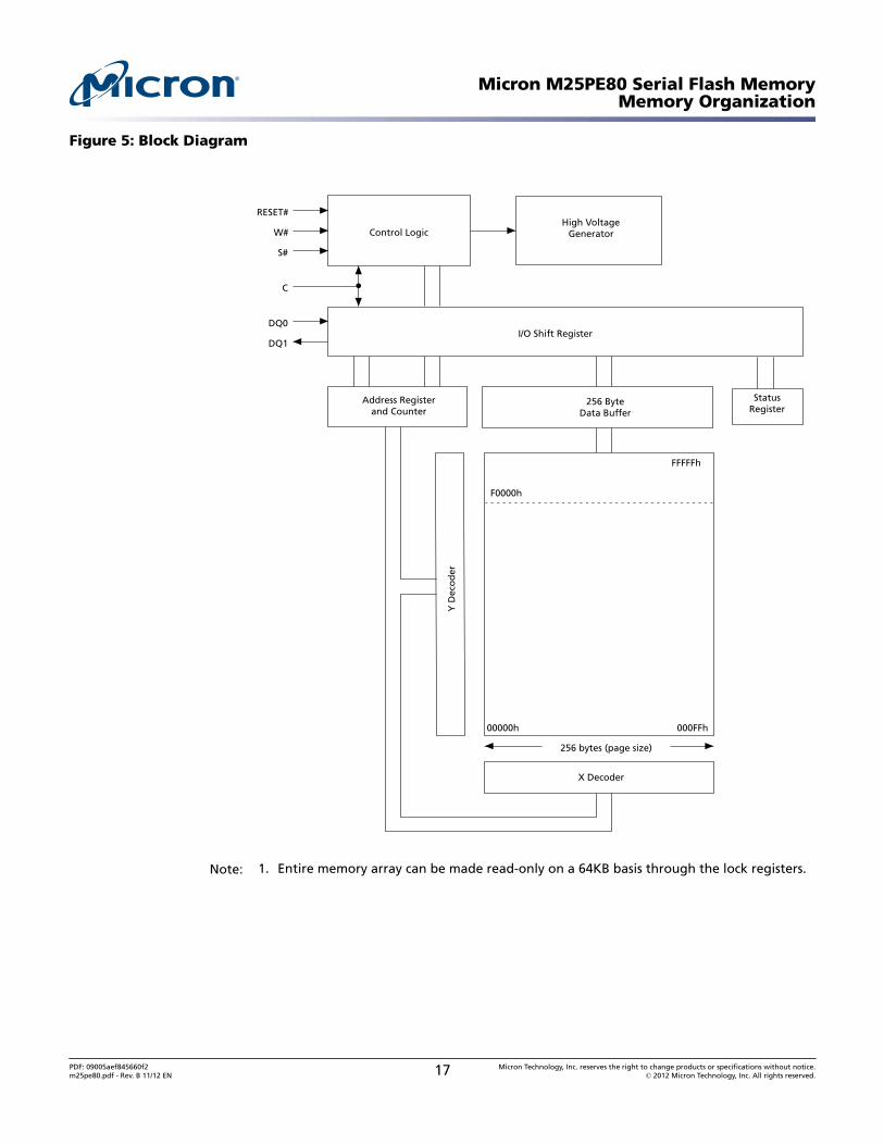
Figure 5: Block Diagram
RESET#
S#
W# Control LogicHigh Voltage
Generator
I/O Shift Register
Address Registerand Counter
256 ByteData Buffer
256 bytes (page size)
X Decoder
Y D
eco
der
C
DQ0
DQ1
StatusRegister
00000h
FFFFFh
F0000h
000FFh
Note: 1. Entire memory array can be made read-only on a 64KB basis through the lock registers.
Micron M25PE80 Serial Flash MemoryMemory Organization
PDF: 09005aef845660f2m25pe80.pdf - Rev. B 11/12 EN 17 Micron Technology, Inc. reserves the right to change products or specifications without notice.
© 2012 Micron Technology, Inc. All rights reserved.
Command Set OverviewAll commands, addresses, and data are shifted in and out of the device, most significantbit first.
Serial data input (DQ1) is sampled on the first rising edge of serial clock (C) after chipselect (S#) is driven LOW. Then, the one-byte command code must be shifted in to thedevice, most significant bit first, on DQ1, each bit being latched on the rising edges of C.
Every command sequence starts with a one-byte command code. Depending on thecommand, this command code might be followed by address or data bytes, by addressand data bytes, or by neither address or data bytes. For the following commands, theshifted-in command sequence is followed by a data-out sequence. S# can be drivenHIGH after any bit of the data-out sequence is being shifted out.
• READ DATA BYTES (READ)• READ DATA BYTES at HIGHER SPEED• READ STATUS REGISTER• READ TO LOCK REGISTER
For the following commands, S# must be driven HIGH exactly at a byte boundary. Thatis, after an exact multiple of eight clock pulses following S# being driven LOW, S# mustbe driven HIGH. Otherwise, the command is rejected and not executed.
• PAGE WRITE• PAGE PROGRAM• PAGE ERASE• SUBSECTOR ERASE• SECTOR ERASE• BULK ERASE• WRITE ENABLE• WRITE DISABLE• WRITE STATUS REGISTER• WRITE TO LOCK REGISTER• DEEP POWER-DOWN• RELEASE FROM DEEP POWER-DOWN
All attempts to access the memory array are ignored during a WRITE cycle, a PROGRAMcycle, or an ERASE cycle. In addition, the internal cycle for each of these commandscontinues unaffected.
Micron M25PE80 Serial Flash MemoryCommand Set Overview
PDF: 09005aef845660f2m25pe80.pdf - Rev. B 11/12 EN 18 Micron Technology, Inc. reserves the right to change products or specifications without notice.
© 2012 Micron Technology, Inc. All rights reserved.
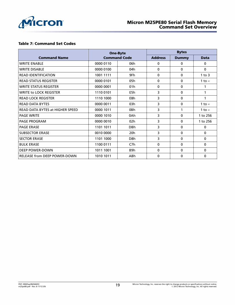
Table 7: Command Set Codes
Command NameOne-Byte
Command Code
Bytes
Address Dummy Data
WRITE ENABLE 0000 0110 06h 0 0 0
WRITE DISABLE 0000 0100 04h 0 0 0
READ IDENTIFICATION 1001 1111 9Fh 0 0 1 to 3
READ STATUS REGISTER 0000 0101 05h 0 0 1 to ∞WRITE STATUS REGISTER 0000 0001 01h 0 0 1
WRITE to LOCK REGISTER 1110 0101 E5h 3 0 1
READ LOCK REGISTER 1110 1000 E8h 3 0 1
READ DATA BYTES 0000 0011 03h 3 0 1 to ∞READ DATA BYTES at HIGHER SPEED 0000 1011 0Bh 3 1 1 to ∞PAGE WRITE 0000 1010 0Ah 3 0 1 to 256
PAGE PROGRAM 0000 0010 02h 3 0 1 to 256
PAGE ERASE 1101 1011 DBh 3 0 0
SUBSECTOR ERASE 0010 0000 20h 3 0 0
SECTOR ERASE 1101 1000 D8h 3 0 0
BULK ERASE 1100 0111 C7h 0 0 0
DEEP POWER-DOWN 1011 1001 B9h 0 0 0
RELEASE from DEEP POWER-DOWN 1010 1011 ABh 0 0 0
Micron M25PE80 Serial Flash MemoryCommand Set Overview
PDF: 09005aef845660f2m25pe80.pdf - Rev. B 11/12 EN 19 Micron Technology, Inc. reserves the right to change products or specifications without notice.
© 2012 Micron Technology, Inc. All rights reserved.
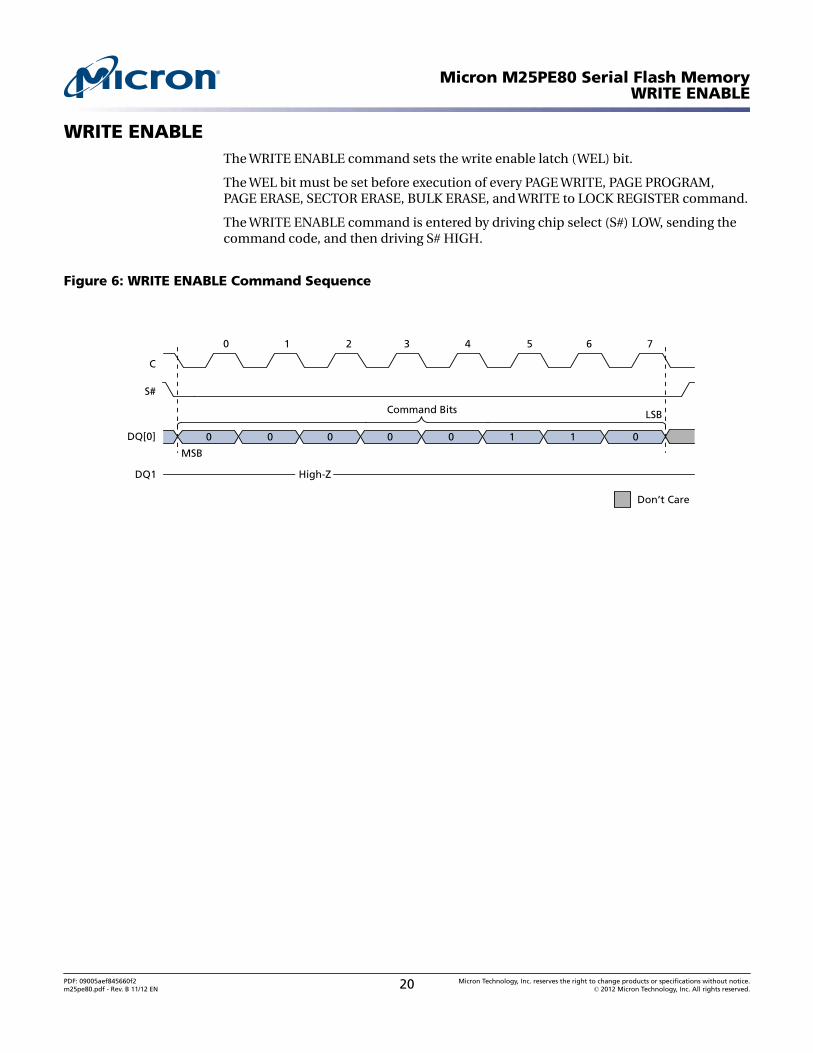
WRITE ENABLEThe WRITE ENABLE command sets the write enable latch (WEL) bit.
The WEL bit must be set before execution of every PAGE WRITE, PAGE PROGRAM,PAGE ERASE, SECTOR ERASE, BULK ERASE, and WRITE to LOCK REGISTER command.
The WRITE ENABLE command is entered by driving chip select (S#) LOW, sending thecommand code, and then driving S# HIGH.
Figure 6: WRITE ENABLE Command Sequence
Don’t Care
DQ[0]
0 1 2 4 53 76
C
High-ZDQ1
MSB
LSB
0 0 0 0 0 011
Command Bits
S#
Micron M25PE80 Serial Flash MemoryWRITE ENABLE
PDF: 09005aef845660f2m25pe80.pdf - Rev. B 11/12 EN 20 Micron Technology, Inc. reserves the right to change products or specifications without notice.
© 2012 Micron Technology, Inc. All rights reserved.
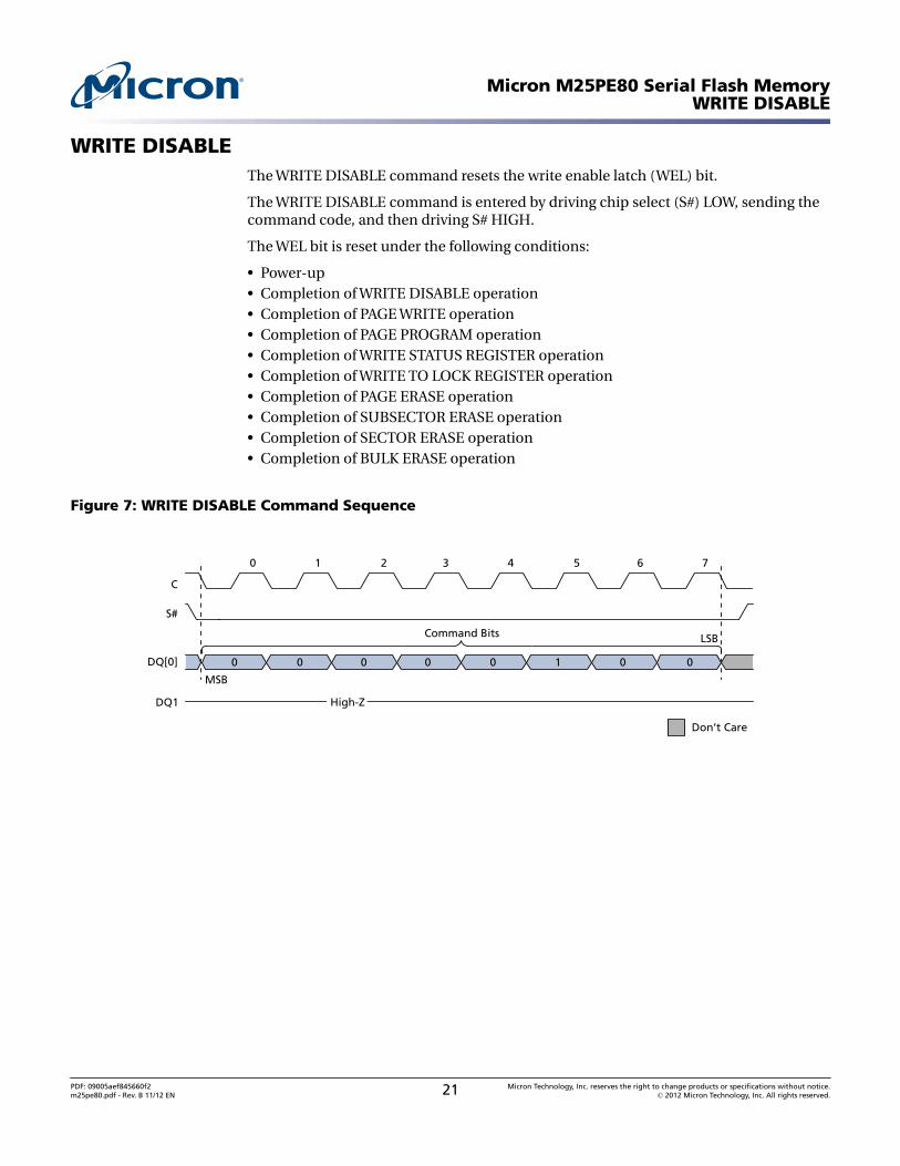
WRITE DISABLEThe WRITE DISABLE command resets the write enable latch (WEL) bit.
The WRITE DISABLE command is entered by driving chip select (S#) LOW, sending thecommand code, and then driving S# HIGH.
The WEL bit is reset under the following conditions:
• Power-up• Completion of WRITE DISABLE operation• Completion of PAGE WRITE operation• Completion of PAGE PROGRAM operation• Completion of WRITE STATUS REGISTER operation• Completion of WRITE TO LOCK REGISTER operation• Completion of PAGE ERASE operation• Completion of SUBSECTOR ERASE operation• Completion of SECTOR ERASE operation• Completion of BULK ERASE operation
Figure 7: WRITE DISABLE Command Sequence
Don’t Care
DQ[0]
0 1 2 4 53 76
C
High-ZDQ1
MSB
LSB
0 0 0 0 0 001
Command Bits
S#
Micron M25PE80 Serial Flash MemoryWRITE DISABLE
PDF: 09005aef845660f2m25pe80.pdf - Rev. B 11/12 EN 21 Micron Technology, Inc. reserves the right to change products or specifications without notice.
© 2012 Micron Technology, Inc. All rights reserved.
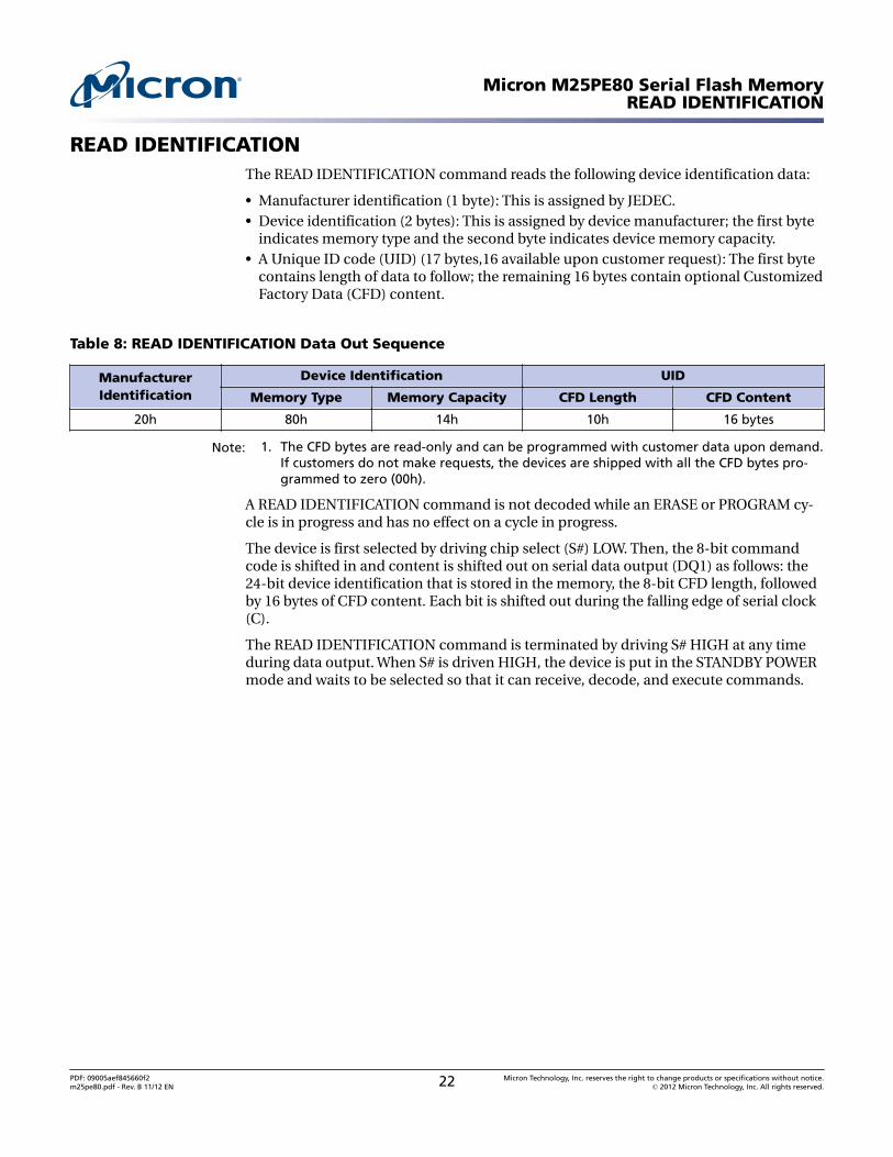
READ IDENTIFICATIONThe READ IDENTIFICATION command reads the following device identification data:
• Manufacturer identification (1 byte): This is assigned by JEDEC.• Device identification (2 bytes): This is assigned by device manufacturer; the first byte
indicates memory type and the second byte indicates device memory capacity.• A Unique ID code (UID) (17 bytes,16 available upon customer request): The first byte
contains length of data to follow; the remaining 16 bytes contain optional CustomizedFactory Data (CFD) content.
Table 8: READ IDENTIFICATION Data Out Sequence
ManufacturerIdentification
Device Identification UID
Memory Type Memory Capacity CFD Length CFD Content
20h 80h 14h 10h 16 bytes
Note: 1. The CFD bytes are read-only and can be programmed with customer data upon demand.If customers do not make requests, the devices are shipped with all the CFD bytes pro-grammed to zero (00h).
A READ IDENTIFICATION command is not decoded while an ERASE or PROGRAM cy-cle is in progress and has no effect on a cycle in progress.
The device is first selected by driving chip select (S#) LOW. Then, the 8-bit commandcode is shifted in and content is shifted out on serial data output (DQ1) as follows: the24-bit device identification that is stored in the memory, the 8-bit CFD length, followedby 16 bytes of CFD content. Each bit is shifted out during the falling edge of serial clock(C).
The READ IDENTIFICATION command is terminated by driving S# HIGH at any timeduring data output. When S# is driven HIGH, the device is put in the STANDBY POWERmode and waits to be selected so that it can receive, decode, and execute commands.
Micron M25PE80 Serial Flash MemoryREAD IDENTIFICATION
PDF: 09005aef845660f2m25pe80.pdf - Rev. B 11/12 EN 22 Micron Technology, Inc. reserves the right to change products or specifications without notice.
© 2012 Micron Technology, Inc. All rights reserved.
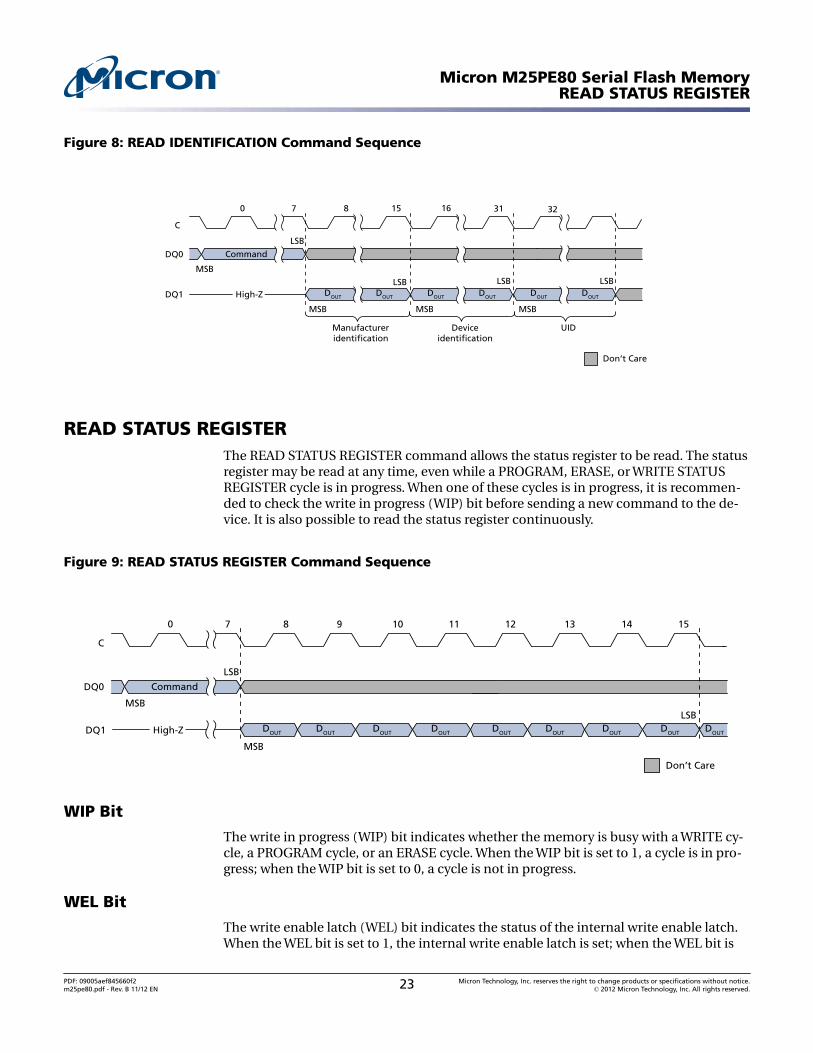
Figure 8: READ IDENTIFICATION Command Sequence
UIDDeviceidentification
Manufactureridentification
High-ZDQ1
MSB MSB
DOUT DOUT DOUT DOUT
LSBLSB
7 8 15 16 32310
C
MSB
DQ0
LSB
Command
MSB
DOUT DOUT
LSB
Don’t Care
READ STATUS REGISTERThe READ STATUS REGISTER command allows the status register to be read. The statusregister may be read at any time, even while a PROGRAM, ERASE, or WRITE STATUSREGISTER cycle is in progress. When one of these cycles is in progress, it is recommen-ded to check the write in progress (WIP) bit before sending a new command to the de-vice. It is also possible to read the status register continuously.
Figure 9: READ STATUS REGISTER Command Sequence
High-ZDQ1
7 8 9 10 11 12 13 14 150
C
MSB
DQ0
LSB
Command
MSB
DOUT DOUT DOUT DOUT DOUT
LSBDOUT DOUT DOUT DOUT
Don’t Care
WIP Bit
The write in progress (WIP) bit indicates whether the memory is busy with a WRITE cy-cle, a PROGRAM cycle, or an ERASE cycle. When the WIP bit is set to 1, a cycle is in pro-gress; when the WIP bit is set to 0, a cycle is not in progress.
WEL Bit
The write enable latch (WEL) bit indicates the status of the internal write enable latch.When the WEL bit is set to 1, the internal write enable latch is set; when the WEL bit is
Micron M25PE80 Serial Flash MemoryREAD STATUS REGISTER
PDF: 09005aef845660f2m25pe80.pdf - Rev. B 11/12 EN 23 Micron Technology, Inc. reserves the right to change products or specifications without notice.
© 2012 Micron Technology, Inc. All rights reserved.
set to 0, the internal write enable latch is reset and no WRITE , PROGRAM, or ERASEcommand is accepted.
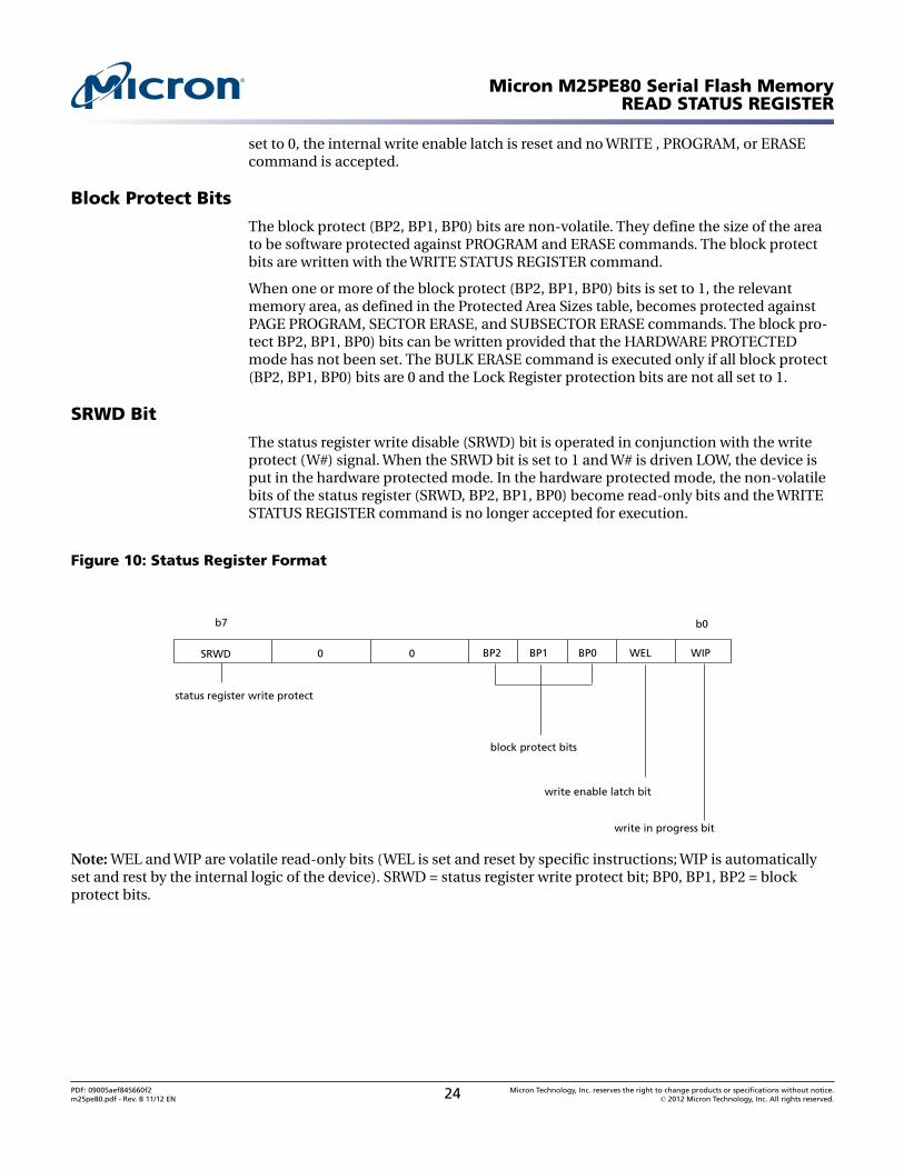
Block Protect Bits
The block protect (BP2, BP1, BP0) bits are non-volatile. They define the size of the areato be software protected against PROGRAM and ERASE commands. The block protectbits are written with the WRITE STATUS REGISTER command.
When one or more of the block protect (BP2, BP1, BP0) bits is set to 1, the relevantmemory area, as defined in the Protected Area Sizes table, becomes protected againstPAGE PROGRAM, SECTOR ERASE, and SUBSECTOR ERASE commands. The block pro-tect BP2, BP1, BP0) bits can be written provided that the HARDWARE PROTECTEDmode has not been set. The BULK ERASE command is executed only if all block protect(BP2, BP1, BP0) bits are 0 and the Lock Register protection bits are not all set to 1.
SRWD Bit
The status register write disable (SRWD) bit is operated in conjunction with the writeprotect (W#) signal. When the SRWD bit is set to 1 and W# is driven LOW, the device isput in the hardware protected mode. In the hardware protected mode, the non-volatilebits of the status register (SRWD, BP2, BP1, BP0) become read-only bits and the WRITESTATUS REGISTER command is no longer accepted for execution.
Figure 10: Status Register Format
b7
SRWD 0 0 BP2 BP1 BP0 WEL WIP
b0
status register write protect
block protect bits
write enable latch bit
write in progress bit
Note: WEL and WIP are volatile read-only bits (WEL is set and reset by specific instructions; WIP is automaticallyset and rest by the internal logic of the device). SRWD = status register write protect bit; BP0, BP1, BP2 = blockprotect bits.
Micron M25PE80 Serial Flash MemoryREAD STATUS REGISTER
PDF: 09005aef845660f2m25pe80.pdf - Rev. B 11/12 EN 24 Micron Technology, Inc. reserves the right to change products or specifications without notice.
© 2012 Micron Technology, Inc. All rights reserved.
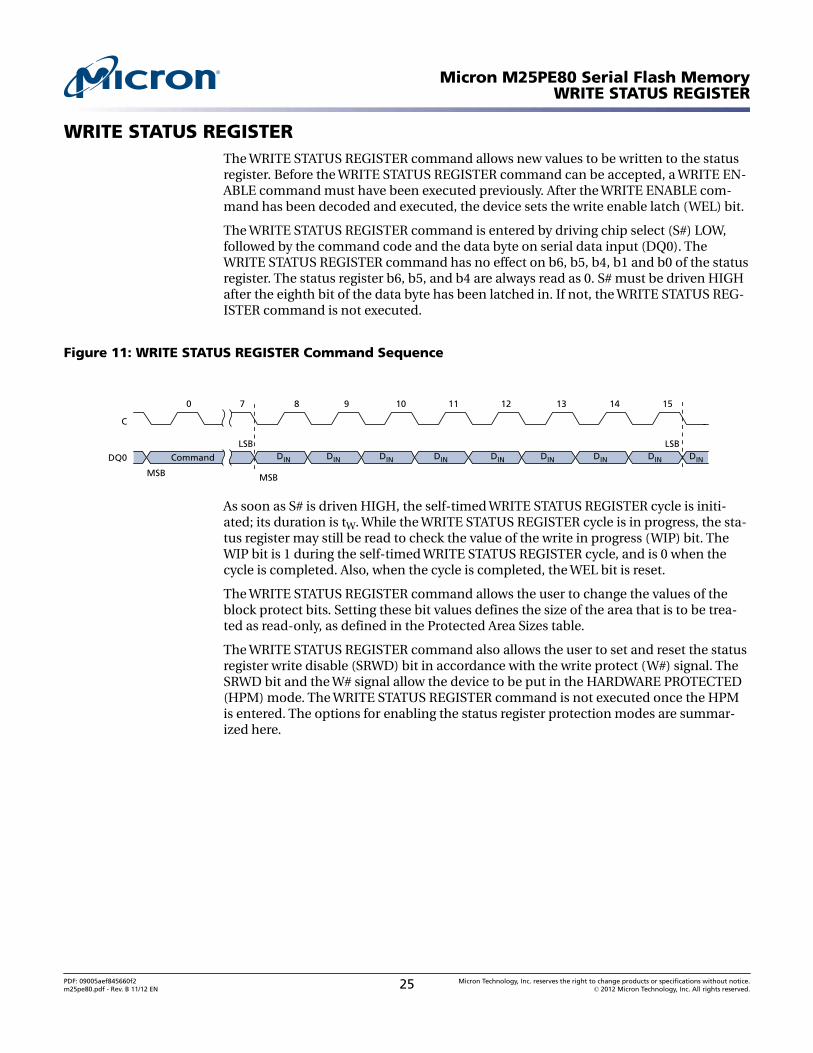
WRITE STATUS REGISTERThe WRITE STATUS REGISTER command allows new values to be written to the statusregister. Before the WRITE STATUS REGISTER command can be accepted, a WRITE EN-ABLE command must have been executed previously. After the WRITE ENABLE com-mand has been decoded and executed, the device sets the write enable latch (WEL) bit.
The WRITE STATUS REGISTER command is entered by driving chip select (S#) LOW,followed by the command code and the data byte on serial data input (DQ0). TheWRITE STATUS REGISTER command has no effect on b6, b5, b4, b1 and b0 of the statusregister. The status register b6, b5, and b4 are always read as 0. S# must be driven HIGHafter the eighth bit of the data byte has been latched in. If not, the WRITE STATUS REG-ISTER command is not executed.
Figure 11: WRITE STATUS REGISTER Command Sequence
7 8 9 10 11 12 13 14 150
C
MSB
DQ0
LSB
Command
MSB
LSBDIN DIN DIN DIN DINDIN DIN DIN DIN
As soon as S# is driven HIGH, the self-timed WRITE STATUS REGISTER cycle is initi-ated; its duration is tW. While the WRITE STATUS REGISTER cycle is in progress, the sta-tus register may still be read to check the value of the write in progress (WIP) bit. TheWIP bit is 1 during the self-timed WRITE STATUS REGISTER cycle, and is 0 when thecycle is completed. Also, when the cycle is completed, the WEL bit is reset.
The WRITE STATUS REGISTER command allows the user to change the values of theblock protect bits. Setting these bit values defines the size of the area that is to be trea-ted as read-only, as defined in the Protected Area Sizes table.
The WRITE STATUS REGISTER command also allows the user to set and reset the statusregister write disable (SRWD) bit in accordance with the write protect (W#) signal. TheSRWD bit and the W# signal allow the device to be put in the HARDWARE PROTECTED(HPM) mode. The WRITE STATUS REGISTER command is not executed once the HPMis entered. The options for enabling the status register protection modes are summar-ized here.
Micron M25PE80 Serial Flash MemoryWRITE STATUS REGISTER
PDF: 09005aef845660f2m25pe80.pdf - Rev. B 11/12 EN 25 Micron Technology, Inc. reserves the right to change products or specifications without notice.
© 2012 Micron Technology, Inc. All rights reserved.
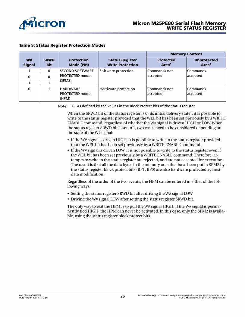
Table 9: Status Register Protection Modes
W#Signal
SRWDBit
ProtectionMode (PM)
Status RegisterWrite Protection
Memory Content
ProtectedArea1
UnprotectedArea1
1 0 SECOND SOFTWAREPROTECTED mode(SPM2)
Software protection Commands notaccepted
Commandsaccepted0 0
1 1
0 1 HARDWAREPROTECTED mode(HPM)
Hardware protection Commands notaccepted
Commandsaccepted
Note: 1. As defined by the values in the Block Protect bits of the status register.
When the SRWD bit of the status register is 0 (its initial delivery state), it is possible towrite to the status register provided that the WEL bit has been set previously by a WRITEENABLE command, regardless of whether the W# signal is driven HIGH or LOW. Whenthe status register SRWD bit is set to 1, two cases need to be considered depending onthe state of the W# signal:
• If the W# signal is driven HIGH, it is possible to write to the status register providedthat the WEL bit has been set previously by a WRITE ENABLE command.
• If the W# signal is driven LOW, it is not possible to write to the status register even ifthe WEL bit has been set previously by a WRITE ENABLE command. Therefore, at-tempts to write to the status register are rejected, and are not accepted for execution.The result is that all the data bytes in the memory area that have been put in SPM2 bythe status register block protect bits (BP1, BP0) are also hardware protected againstdata modification.
Regardless of the order of the two events, the HPM can be entered in either of the fol-lowing ways:
• Setting the status register SRWD bit after driving the W# signal LOW• Driving the W# signal LOW after setting the status register SRWD bit.
The only way to exit the HPM is to pull the W# signal HIGH. If the W# signal is perma-nently tied HIGH, the HPM can never be activated. In this case, only the SPM2 is availa-ble, using the status register block protect bits.
Micron M25PE80 Serial Flash MemoryWRITE STATUS REGISTER
PDF: 09005aef845660f2m25pe80.pdf - Rev. B 11/12 EN 26 Micron Technology, Inc. reserves the right to change products or specifications without notice.
© 2012 Micron Technology, Inc. All rights reserved.
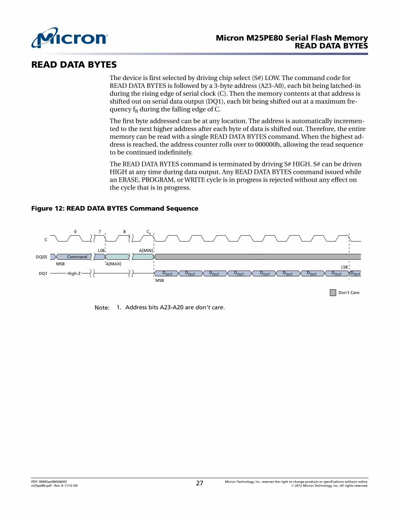
READ DATA BYTESThe device is first selected by driving chip select (S#) LOW. The command code forREAD DATA BYTES is followed by a 3-byte address (A23-A0), each bit being latched-induring the rising edge of serial clock (C). Then the memory contents at that address isshifted out on serial data output (DQ1), each bit being shifted out at a maximum fre-quency fR during the falling edge of C.
The first byte addressed can be at any location. The address is automatically incremen-ted to the next higher address after each byte of data is shifted out. Therefore, the entirememory can be read with a single READ DATA BYTES command. When the highest ad-dress is reached, the address counter rolls over to 000000h, allowing the read sequenceto be continued indefinitely.
The READ DATA BYTES command is terminated by driving S# HIGH. S# can be drivenHIGH at any time during data output. Any READ DATA BYTES command issued whilean ERASE, PROGRAM, or WRITE cycle is in progress is rejected without any effect onthe cycle that is in progress.
Figure 12: READ DATA BYTES Command Sequence
Don’t Care
MSB
DQ[0]
LSB
Command
A[MAX]
A[MIN]
7 8 Cx0
C
High-ZDQ1
MSB
DOUT DOUT DOUT DOUT DOUT
LSBDOUT DOUT DOUT DOUT
Note: 1. Address bits A23-A20 are don't care.
Micron M25PE80 Serial Flash MemoryREAD DATA BYTES
PDF: 09005aef845660f2m25pe80.pdf - Rev. B 11/12 EN 27 Micron Technology, Inc. reserves the right to change products or specifications without notice.
© 2012 Micron Technology, Inc. All rights reserved.
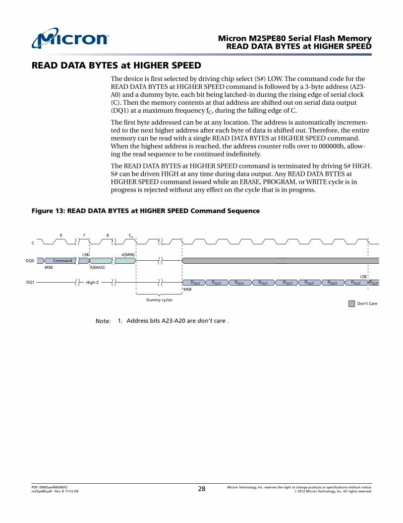
READ DATA BYTES at HIGHER SPEEDThe device is first selected by driving chip select (S#) LOW. The command code for theREAD DATA BYTES at HIGHER SPEED command is followed by a 3-byte address (A23-A0) and a dummy byte, each bit being latched-in during the rising edge of serial clock(C). Then the memory contents at that address are shifted out on serial data output(DQ1) at a maximum frequency fC, during the falling edge of C.
The first byte addressed can be at any location. The address is automatically incremen-ted to the next higher address after each byte of data is shifted out. Therefore, the entirememory can be read with a single READ DATA BYTES at HIGHER SPEED command.When the highest address is reached, the address counter rolls over to 000000h, allow-ing the read sequence to be continued indefinitely.
The READ DATA BYTES at HIGHER SPEED command is terminated by driving S# HIGH.S# can be driven HIGH at any time during data output. Any READ DATA BYTES atHIGHER SPEED command issued while an ERASE, PROGRAM, or WRITE cycle is inprogress is rejected without any effect on the cycle that is in progress.
Figure 13: READ DATA BYTES at HIGHER SPEED Command Sequence
7 8 Cx0
C
MSB
DQ0
LSB
Command
A[MAX]
A[MIN]
MSB
DOUT DOUT DOUT DOUT DOUT
LSBDOUT DOUT DOUT DOUT
Dummy cycles
DQ1 High-Z
Don’t Care
Note: 1. Address bits A23-A20 are don't care .
Micron M25PE80 Serial Flash MemoryREAD DATA BYTES at HIGHER SPEED
PDF: 09005aef845660f2m25pe80.pdf - Rev. B 11/12 EN 28 Micron Technology, Inc. reserves the right to change products or specifications without notice.
© 2012 Micron Technology, Inc. All rights reserved.
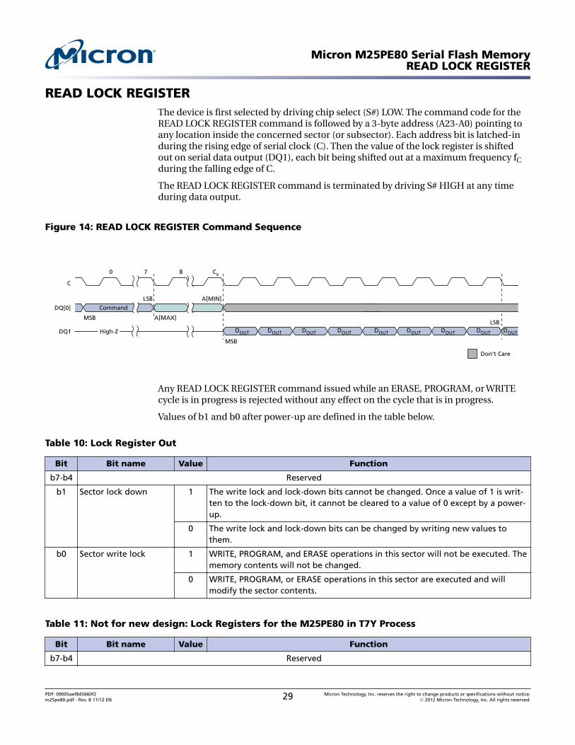
READ LOCK REGISTERThe device is first selected by driving chip select (S#) LOW. The command code for theREAD LOCK REGISTER command is followed by a 3-byte address (A23-A0) pointing toany location inside the concerned sector (or subsector). Each address bit is latched-induring the rising edge of serial clock (C). Then the value of the lock register is shiftedout on serial data output (DQ1), each bit being shifted out at a maximum frequency fCduring the falling edge of C.
The READ LOCK REGISTER command is terminated by driving S# HIGH at any timeduring data output.
Figure 14: READ LOCK REGISTER Command Sequence
MSB
DQ[0]
LSB
Command
A[MAX]
A[MIN]
7 8 Cx0
C
High-ZDQ1
MSB
DOUT DOUT DOUT DOUT DOUT
LSBDOUT DOUT DOUT DOUT
Don’t Care
Any READ LOCK REGISTER command issued while an ERASE, PROGRAM, or WRITEcycle is in progress is rejected without any effect on the cycle that is in progress.
Values of b1 and b0 after power-up are defined in the table below.
Table 10: Lock Register Out
Bit Bit name Value Function
b7-b4 Reserved
b1 Sector lock down 1 The write lock and lock-down bits cannot be changed. Once a value of 1 is writ-ten to the lock-down bit, it cannot be cleared to a value of 0 except by a power-up.
0 The write lock and lock-down bits can be changed by writing new values tothem.
b0 Sector write lock 1 WRITE, PROGRAM, and ERASE operations in this sector will not be executed. Thememory contents will not be changed.
0 WRITE, PROGRAM, or ERASE operations in this sector are executed and willmodify the sector contents.
Table 11: Not for new design: Lock Registers for the M25PE80 in T7Y Process
Bit Bit name Value Function
b7-b4 Reserved
Micron M25PE80 Serial Flash MemoryREAD LOCK REGISTER
PDF: 09005aef845660f2m25pe80.pdf - Rev. B 11/12 EN 29 Micron Technology, Inc. reserves the right to change products or specifications without notice.
© 2012 Micron Technology, Inc. All rights reserved.
Table 11: Not for new design: Lock Registers for the M25PE80 in T7Y Process (Continued)
Bit Bit name Value Function
b3 Subsector lock down 1 This functionality must not be used for new designs, as the M25PE80 deliveredfrom Feb 2007 will not offer this functionality. The write lock and lock down bitscannot be changed. Once a 1 is written to the lock down bit it cannot be clearedto 0 except by a reset or power-up.
0 This functionality must not be used for new designs, as the M25PE80 deliveredfrom Feb 2007 will not offer this functionality. The write lock and lock down bitscan be changed by writing new values to them (default value).
b2 Subsector write lock 1 This functionality must not be used for new designs, as the M25PE80 deliveredfrom Feb 2007 will not offer this functionality. WRITE, PROGRAM, and ERASE op-erations in this subsector will not be executed. The memory contents will not bechanged.
0 This functionality must not be used for new designs, as the M25PE80 deliveredfrom Feb 2007 will not offer this functionality. WRITE, PROGRAM, and ERASE op-erations in this subsector are executed and will modify the subsector contents(default value).
b1 Sector lock down 1 The write lock and lock-down bits cannot be changed. Once a value of 1 is writ-ten to the lock-down bit, it cannot be cleared to a value of 0 except by a reset orpower-up.
0 The write lock and lock-down bits can be changed by writing new values tothem (default value) .
b0 Sector write lock 1 WRITE, PROGRAM, and ERASE operations in this sector will not be executed. Thememory contents will not be changed.
0 WRITE, PROGRAM, or ERASE operations in this sector are executed and willmodify the sector contents (default value).
Note: 1. Subsector write lock is valid for sector 0 and 15 only (the value 0 is returned for othersectors).
Micron M25PE80 Serial Flash MemoryREAD LOCK REGISTER
PDF: 09005aef845660f2m25pe80.pdf - Rev. B 11/12 EN 30 Micron Technology, Inc. reserves the right to change products or specifications without notice.
© 2012 Micron Technology, Inc. All rights reserved.
PAGE WRITEThe PAGE WRITE command allows bytes in the memory to be programmed. Before aPAGE WRITE command can be accepted a WRITE ENABLE command must be execu-ted. After the WRITE ENABLE command has been decoded, the device sets the write en-able latch (WEL) bit.
The PAGE WRITE command is entered by driving chip select (S#) LOW, followed by thecommand code, three address bytes, and at least one data byte on serial data input(DQ0). The reset of the page remains unchanged if no power failure occurs during thiswrite cycle.
The PAGE WRITE command performs a page erase cycle even if only one byte is upda-ted.
If the eight least-significant address bits (A7-A0) are not all zero, all transmitted datathat goes beyond the end of the current page are programmed from the start address ofthe same page; that is, from the address whose eight least significant bits (A7-A0) are allzero. S# must be driven LOW for the entire duration of the sequence.
If more than 256 bytes are sent to the device, previously latched data is discarded andthe last 256 data bytes are guaranteed to be programmed correctly within the samepage. If less than 256 data bytes are sent to device, they are correctly programmed at therequested addresses without any effects on the other bytes of the same page.
For optimized timings, it is recommended to use the PAGE WRITE command to pro-gram all consecutive targeted bytes in a single sequence rather than to use several PAGEWRITE sequences, each containing only a few bytes.
S# must be driven HIGH after the eighth bit of the last data byte has been latched in.Otherwise the PAGE WRITE command is not executed.
As soon as S# is driven HIGH, the self-timed PAGE WRITE cycle is initiated. While thePAGE WRITE cycle is in progress, the status register may be read to check the value ofthe write in progress (WIP) bit. The WIP bit is 1 during the self-timed PAGE WRITE cy-cle, and 0 when the cycle is completed. At some unspecified time before the cycle iscompleted, the write enable latch (WEL) bit is reset.
A PAGE WRITE command applied to a page that is hardware or software protected isnot executed.
Any PAGE WRITE command while an ERASE, PROGRAM, or WRITE cycle is in progressis rejected without having any effects on the cycle that is in progress.
If RESET is drive LOW while a PAGE WRITE cycle is in progress, the PAGE WRITE cycle isinterrupted and the programmed data may be corrupted. On RESET going LOW, the de-vice enters the reset mode and a time of tRHSL is then required before the device can berescheduled by selecting Chip Select (S#) LOW.
Micron M25PE80 Serial Flash MemoryPAGE WRITE
PDF: 09005aef845660f2m25pe80.pdf - Rev. B 11/12 EN 31 Micron Technology, Inc. reserves the right to change products or specifications without notice.
© 2012 Micron Technology, Inc. All rights reserved.
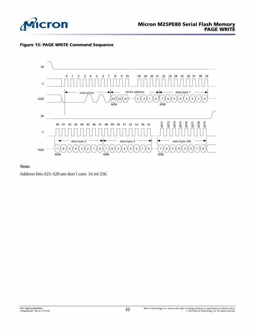
Figure 15: PAGE WRITE Command Sequence
C
DQ0
S#
DQ0
S#
instruction
4241 43 44 45 46 4740 48 49 50 52 53 54 5551
data byte 2 data byte 3 data byte 256
2079
2078
2077
2076
2075
2074
2073
2072
MSB MSB
MSB
24-bit address data byte 1
23 22 21 3 2 1 0
C
0 1 2 3 4 5 6 7 8 9 10 28 29 30 31 32 33 34 35 36 37 38 39
7 6 5 4 3 2 01 7 6 5 4 3 2 01
MSB MSB
7 6 5 4 3 2 01
7 6 5 4 3 2 01
Note:
Address bits A23-A20 are don't care. 1≤ n≤ 256.
Micron M25PE80 Serial Flash MemoryPAGE WRITE
PDF: 09005aef845660f2m25pe80.pdf - Rev. B 11/12 EN 32 Micron Technology, Inc. reserves the right to change products or specifications without notice.
© 2012 Micron Technology, Inc. All rights reserved.
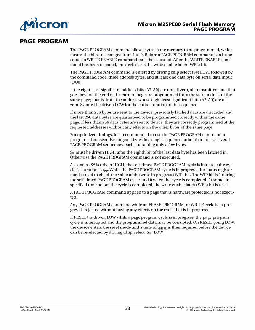
PAGE PROGRAMThe PAGE PROGRAM command allows bytes in the memory to be programmed, whichmeans the bits are changed from 1 to 0. Before a PAGE PROGRAM command can be ac-cepted a WRITE ENABLE command must be executed. After the WRITE ENABLE com-mand has been decoded, the device sets the write enable latch (WEL) bit.
The PAGE PROGRAM command is entered by driving chip select (S#) LOW, followed bythe command code, three address bytes, and at least one data byte on serial data input(DQ0).
If the eight least significant address bits (A7-A0) are not all zero, all transmitted data thatgoes beyond the end of the current page are programmed from the start address of thesame page; that is, from the address whose eight least significant bits (A7-A0) are allzero. S# must be driven LOW for the entire duration of the sequence.
If more than 256 bytes are sent to the device, previously latched data are discarded andthe last 256 data bytes are guaranteed to be programmed correctly within the samepage. If less than 256 data bytes are sent to device, they are correctly programmed at therequested addresses without any effects on the other bytes of the same page.
For optimized timings, it is recommended to use the PAGE PROGRAM command toprogram all consecutive targeted bytes in a single sequence rather than to use severalPAGE PROGRAM sequences, each containing only a few bytes.
S# must be driven HIGH after the eighth bit of the last data byte has been latched in.Otherwise the PAGE PROGRAM command is not executed.
As soon as S# is driven HIGH, the self-timed PAGE PROGRAM cycle is initiated; the cy-cles's duration is tPP. While the PAGE PROGRAM cycle is in progress, the status registermay be read to check the value of the write in progress (WIP) bit. The WIP bit is 1 duringthe self-timed PAGE PROGRAM cycle, and 0 when the cycle is completed. At some un-specified time before the cycle is completed, the write enable latch (WEL) bit is reset.
A PAGE PROGRAM command applied to a page that is hardware protected is not execu-ted.
Any PAGE PROGRAM command while an ERASE, PROGRAM, or WRITE cycle is in pro-gress is rejected without having any effects on the cycle that is in progress.
If RESET# is driven LOW while a page program cycle is in progress, the page programcycle is interrupted and the programmed data may be corrupted. On RESET going LOW,the device enters the reset mode and a time of tRHSL is then required before the devicecan be reselected by driving Chip Select (S#) LOW.
Micron M25PE80 Serial Flash MemoryPAGE PROGRAM
PDF: 09005aef845660f2m25pe80.pdf - Rev. B 11/12 EN 33 Micron Technology, Inc. reserves the right to change products or specifications without notice.
© 2012 Micron Technology, Inc. All rights reserved.
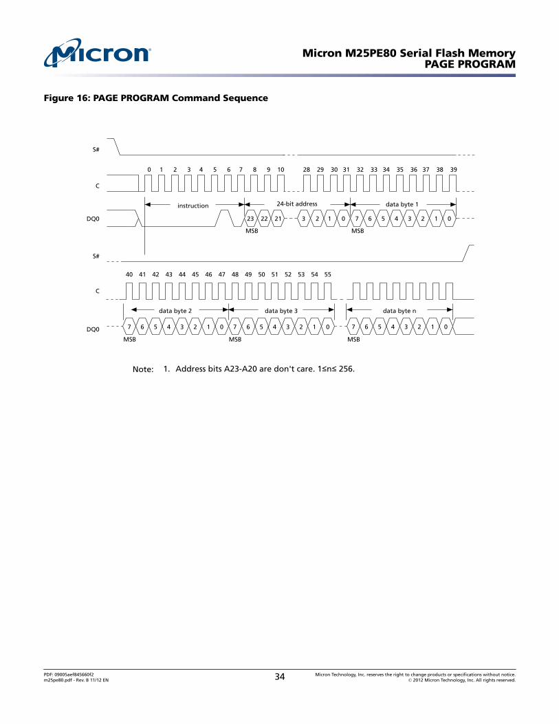
Figure 16: PAGE PROGRAM Command Sequence
C
DQ0
S#
DQ0
S#
instruction
4241 43 44 45 46 4740 48 49 50 52 53 54 5551
data byte 2 data byte 3 data byte n
MSB MSB
MSB
24-bit address data byte 1
23 22 21 3 2 1 0
C
0 1 2 3 4 5 6 7 8 9 10 28 29 30 31 32 33 34 35 36 37 38 39
7 6 5 4 3 2 01 7 6 5 4 3 2 01
MSB MSB
7 6 5 4 3 2 01
7 6 5 4 3 2 01
Note: 1. Address bits A23-A20 are don't care. 1≤n≤ 256.
Micron M25PE80 Serial Flash MemoryPAGE PROGRAM
PDF: 09005aef845660f2m25pe80.pdf - Rev. B 11/12 EN 34 Micron Technology, Inc. reserves the right to change products or specifications without notice.
© 2012 Micron Technology, Inc. All rights reserved.
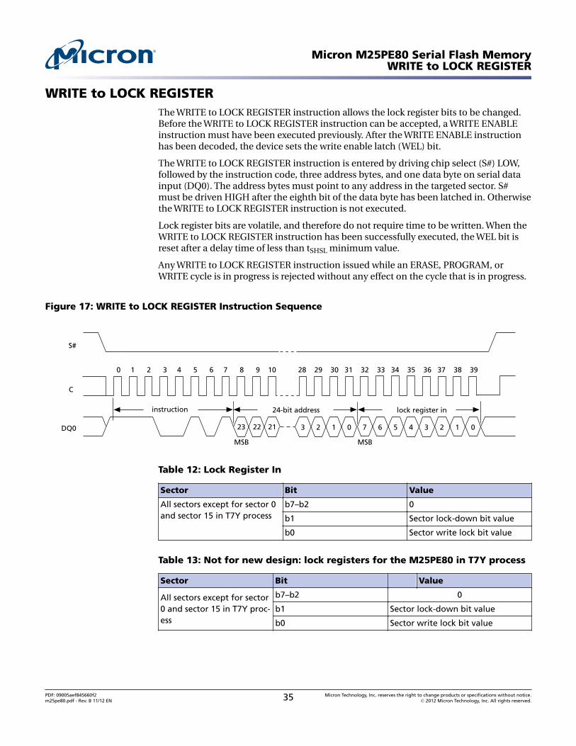
WRITE to LOCK REGISTERThe WRITE to LOCK REGISTER instruction allows the lock register bits to be changed.Before the WRITE to LOCK REGISTER instruction can be accepted, a WRITE ENABLEinstruction must have been executed previously. After the WRITE ENABLE instructionhas been decoded, the device sets the write enable latch (WEL) bit.
The WRITE to LOCK REGISTER instruction is entered by driving chip select (S#) LOW,followed by the instruction code, three address bytes, and one data byte on serial datainput (DQ0). The address bytes must point to any address in the targeted sector. S#must be driven HIGH after the eighth bit of the data byte has been latched in. Otherwisethe WRITE to LOCK REGISTER instruction is not executed.
Lock register bits are volatile, and therefore do not require time to be written. When theWRITE to LOCK REGISTER instruction has been successfully executed, the WEL bit isreset after a delay time of less than tSHSL minimum value.
Any WRITE to LOCK REGISTER instruction issued while an ERASE, PROGRAM, orWRITE cycle is in progress is rejected without any effect on the cycle that is in progress.
Figure 17: WRITE to LOCK REGISTER Instruction Sequence
DQ0
S#
instruction
MSB MSB
24-bit address lock register in
23 22 21 3 2 01 7 6 5 4 3 2 01
C
0 1 2 3 4 5 6 7 8 9 10 28 29 30 31 32 33 34 35 36 37 38 39
Table 12: Lock Register In
Sector Bit Value
All sectors except for sector 0and sector 15 in T7Y process
b7–b2 0
b1 Sector lock-down bit value
b0 Sector write lock bit value
Table 13: Not for new design: lock registers for the M25PE80 in T7Y process
Sector Bit Value
All sectors except for sector0 and sector 15 in T7Y proc-ess
b7–b2 0
b1 Sector lock-down bit value
b0 Sector write lock bit value
Micron M25PE80 Serial Flash MemoryWRITE to LOCK REGISTER
PDF: 09005aef845660f2m25pe80.pdf - Rev. B 11/12 EN 35 Micron Technology, Inc. reserves the right to change products or specifications without notice.
© 2012 Micron Technology, Inc. All rights reserved.
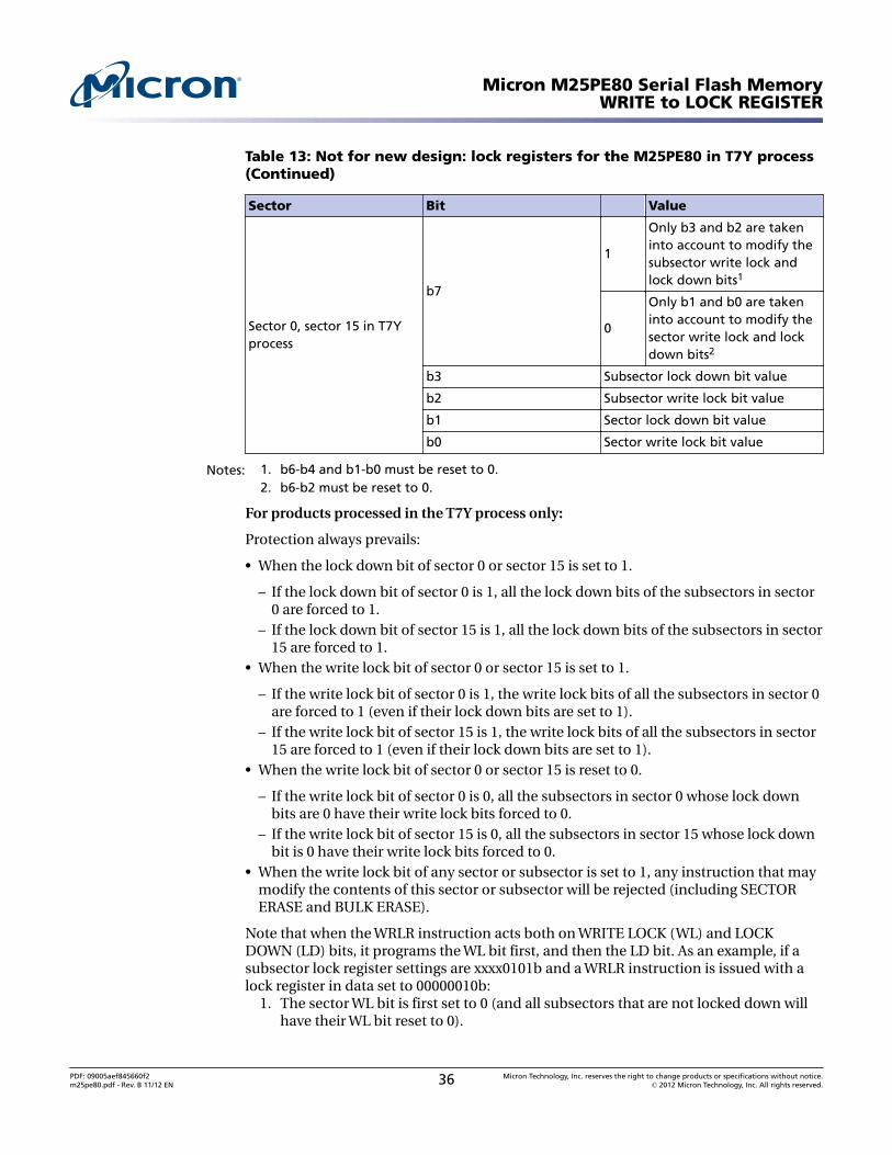
Table 13: Not for new design: lock registers for the M25PE80 in T7Y process(Continued)
Sector Bit Value
Sector 0, sector 15 in T7Yprocess
b7
1
Only b3 and b2 are takeninto account to modify thesubsector write lock andlock down bits1
0
Only b1 and b0 are takeninto account to modify thesector write lock and lockdown bits2
b3 Subsector lock down bit value
b2 Subsector write lock bit value
b1 Sector lock down bit value
b0 Sector write lock bit value
Notes: 1. b6-b4 and b1-b0 must be reset to 0.2. b6-b2 must be reset to 0.
For products processed in the T7Y process only:
Protection always prevails:
• When the lock down bit of sector 0 or sector 15 is set to 1.
– If the lock down bit of sector 0 is 1, all the lock down bits of the subsectors in sector0 are forced to 1.
– If the lock down bit of sector 15 is 1, all the lock down bits of the subsectors in sector15 are forced to 1.
• When the write lock bit of sector 0 or sector 15 is set to 1.
– If the write lock bit of sector 0 is 1, the write lock bits of all the subsectors in sector 0are forced to 1 (even if their lock down bits are set to 1).
– If the write lock bit of sector 15 is 1, the write lock bits of all the subsectors in sector15 are forced to 1 (even if their lock down bits are set to 1).
• When the write lock bit of sector 0 or sector 15 is reset to 0.
– If the write lock bit of sector 0 is 0, all the subsectors in sector 0 whose lock downbits are 0 have their write lock bits forced to 0.
– If the write lock bit of sector 15 is 0, all the subsectors in sector 15 whose lock downbit is 0 have their write lock bits forced to 0.
• When the write lock bit of any sector or subsector is set to 1, any instruction that maymodify the contents of this sector or subsector will be rejected (including SECTORERASE and BULK ERASE).
Note that when the WRLR instruction acts both on WRITE LOCK (WL) and LOCKDOWN (LD) bits, it programs the WL bit first, and then the LD bit. As an example, if asubsector lock register settings are xxxx0101b and a WRLR instruction is issued with alock register in data set to 00000010b:
1. The sector WL bit is first set to 0 (and all subsectors that are not locked down willhave their WL bit reset to 0).
Micron M25PE80 Serial Flash MemoryWRITE to LOCK REGISTER
PDF: 09005aef845660f2m25pe80.pdf - Rev. B 11/12 EN 36 Micron Technology, Inc. reserves the right to change products or specifications without notice.
© 2012 Micron Technology, Inc. All rights reserved.
2. The sector LD bit and all subsectors LD bits are set to 1. In this case, the final valueof the above subsector lock register is xxxx1010b.
Micron M25PE80 Serial Flash MemoryWRITE to LOCK REGISTER
PDF: 09005aef845660f2m25pe80.pdf - Rev. B 11/12 EN 37 Micron Technology, Inc. reserves the right to change products or specifications without notice.
© 2012 Micron Technology, Inc. All rights reserved.
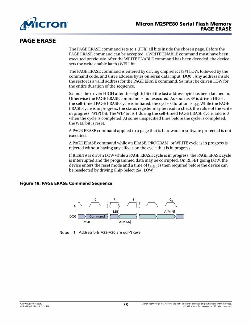
PAGE ERASEThe PAGE ERASE command sets to 1 (FFh) all bits inside the chosen page. Before thePAGE ERASE command can be accepted, a WRITE ENABLE command must have beenexecuted previously. After the WRITE ENABLE command has been decoded, the devicesets the write enable latch (WEL) bit.
The PAGE ERASE command is entered by driving chip select (S#) LOW, followed by thecommand code, and three address bytes on serial data input (DQ0). Any address insidethe sector is a valid address for the PAGE ERASE command. S# must be driven LOW forthe entire duration of the sequence.
S# must be driven HIGH after the eighth bit of the last address byte has been latched in.Otherwise the PAGE ERASE command is not executed. As soon as S# is driven HIGH,the self-timed PAGE ERASE cycle is initiated; the cycle's duration is tPE. While the PAGEERASE cycle is in progress, the status register may be read to check the value of the writein progress (WIP) bit. The WIP bit is 1 during the self-timed PAGE ERASE cycle, and is 0when the cycle is completed. At some unspecified time before the cycle is completed,the WEL bit is reset.
A PAGE ERASE command applied to a page that is hardware or software protected is notexecuted.
A PAGE ERASE command while an ERASE, PROGRAM, or WRITE cycle is in progress isrejected without having any effects on the cycle that is in progress.
If RESET# is driven LOW while a PAGE ERASE cycle is in progress, the PAGE ERASE cycleis interrupted and the programmed data may be corrupted. On RESET going LOW, thedevice enters the reset mode and a time of tRHSL is then required before the device canbe reselected by driving Chip Select (S#) LOW.
Figure 18: PAGE ERASE Command Sequence
7 8 Cx0
C
MSB
DQ0
LSB
Command
A[MAX]
A[MIN]
Note: 1. Address bits A23-A20 are don't care.
Micron M25PE80 Serial Flash MemoryPAGE ERASE
PDF: 09005aef845660f2m25pe80.pdf - Rev. B 11/12 EN 38 Micron Technology, Inc. reserves the right to change products or specifications without notice.
© 2012 Micron Technology, Inc. All rights reserved.
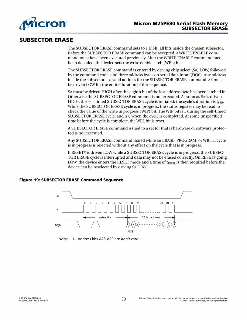
SUBSECTOR ERASEThe SUBSECTOR ERASE command sets to 1 (FFh) all bits inside the chosen subsector.Before the SUBSECTOR ERASE command can be accepted, a WRITE ENABLE com-mand must have been executed previously. After the WRITE ENABLE command hasbeen decoded, the device sets the write enable latch (WEL) bit.
The SUBSECTOR ERASE command is entered by driving chip select (S#) LOW, followedby the command code, and three address bytes on serial data input (DQ0). Any addressinside the subsector is a valid address for the SUBSECTOR ERASE command. S# mustbe driven LOW for the entire duration of the sequence.
S# must be driven HIGH after the eighth bit of the last address byte has been latched in.Otherwise the SUBSECTOR ERASE command is not executed. As soon as S# is drivenHIGH, the self-timed SUBSECTOR ERASE cycle is initiated; the cycle's duration is tSSE.While the SUBSECTOR ERASE cycle is in progress, the status register may be read tocheck the value of the write in progress (WIP) bit. The WIP bit is 1 during the self-timedSUBSECTOR ERASE cycle, and is 0 when the cycle is completed. At some unspecifiedtime before the cycle is complete, the WEL bit is reset.
A SUBSECTOR ERASE command issued to a sector that is hardware or software protec-ted is not executed.
Any SUBSECTOR ERASE command issued while an ERASE, PROGRAM, or WRITE cycleis in progress is rejected without any effect on the cycle that is in progress.
If RESET# is driven LOW while a SUBSECTOR ERASE cycle is in progress, the SUBSEC-TOR ERASE cycle is interrupted and data may not be erased correctly. On RESET# goingLOW, the device enters the RESET mode and a time of tRHSL is then required before thedevice can be reselected by driving S# LOW.
Figure 19: SUBSECTOR ERASE Command Sequence
DQ0
24 bit address
C
S#
instruction
23 22 2 01
MSB
21 3 4 5 6 7 8 9 29 30 310
Note: 1. Address bits A23-A20 are don't care.
Micron M25PE80 Serial Flash MemorySUBSECTOR ERASE
PDF: 09005aef845660f2m25pe80.pdf - Rev. B 11/12 EN 39 Micron Technology, Inc. reserves the right to change products or specifications without notice.
© 2012 Micron Technology, Inc. All rights reserved.
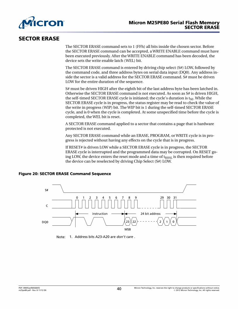
SECTOR ERASEThe SECTOR ERASE command sets to 1 (FFh) all bits inside the chosen sector. Beforethe SECTOR ERASE command can be accepted, a WRITE ENABLE command must havebeen executed previously. After the WRITE ENABLE command has been decoded, thedevice sets the write enable latch (WEL) bit.
The SECTOR ERASE command is entered by driving chip select (S#) LOW, followed bythe command code, and three address bytes on serial data input (DQ0). Any address in-side the sector is a valid address for the SECTOR ERASE command. S# must be drivenLOW for the entire duration of the sequence.
S# must be driven HIGH after the eighth bit of the last address byte has been latched in.Otherwise the SECTOR ERASE command is not executed. As soon as S# is driven HIGH,the self-timed SECTOR ERASE cycle is initiated; the cycle's duration is tSE. While theSECTOR ERASE cycle is in progress, the status register may be read to check the value ofthe write in progress (WIP) bit. The WIP bit is 1 during the self-timed SECTOR ERASEcycle, and is 0 when the cycle is completed. At some unspecified time before the cycle iscompleted, the WEL bit is reset.
A SECTOR ERASE command applied to a sector that contains a page that is hardwareprotected is not executed.
Any SECTOR ERASE command while an ERASE, PROGRAM, or WRITE cycle is in pro-gress is rejected without having any effects on the cycle that is in progress.
If RESET# is driven LOW while a SECTOR ERASE cycle is in progress, the SECTORERASE cycle is interrupted and the programmed data may be corrupted. On RESET go-ing LOW, the device enters the reset mode and a time of tRHSL is then required beforethe device can be reselected by driving Chip Select (S#) LOW.
Figure 20: SECTOR ERASE Command Sequence
24 bit address
C
DQ0
S#
instruction
23 22 2 01
MSB
21 3 4 5 6 7 8 9 29 30 310
Note: 1. Address bits A23-A20 are don't care .
Micron M25PE80 Serial Flash MemorySECTOR ERASE
PDF: 09005aef845660f2m25pe80.pdf - Rev. B 11/12 EN 40 Micron Technology, Inc. reserves the right to change products or specifications without notice.
© 2012 Micron Technology, Inc. All rights reserved.
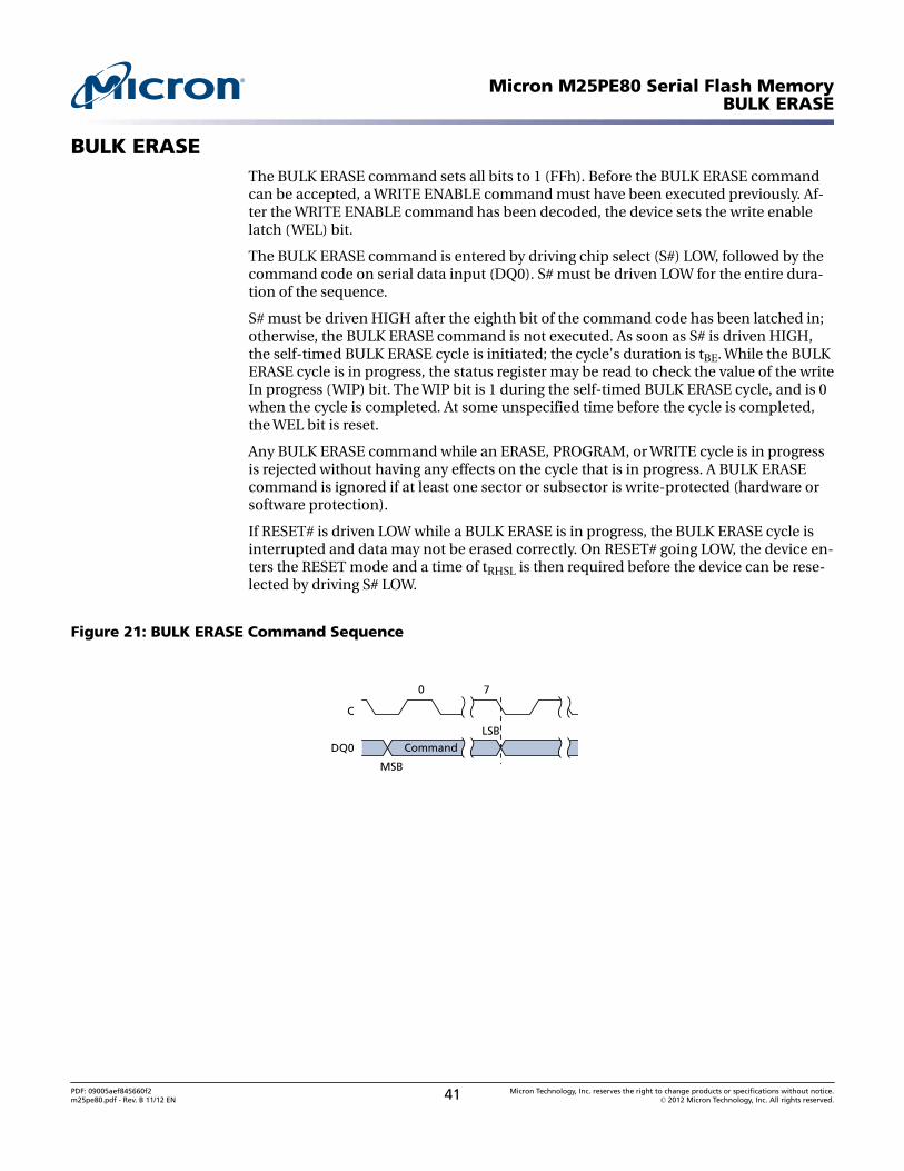
BULK ERASEThe BULK ERASE command sets all bits to 1 (FFh). Before the BULK ERASE commandcan be accepted, a WRITE ENABLE command must have been executed previously. Af-ter the WRITE ENABLE command has been decoded, the device sets the write enablelatch (WEL) bit.
The BULK ERASE command is entered by driving chip select (S#) LOW, followed by thecommand code on serial data input (DQ0). S# must be driven LOW for the entire dura-tion of the sequence.
S# must be driven HIGH after the eighth bit of the command code has been latched in;otherwise, the BULK ERASE command is not executed. As soon as S# is driven HIGH,the self-timed BULK ERASE cycle is initiated; the cycle's duration is tBE. While the BULKERASE cycle is in progress, the status register may be read to check the value of the writeIn progress (WIP) bit. The WIP bit is 1 during the self-timed BULK ERASE cycle, and is 0when the cycle is completed. At some unspecified time before the cycle is completed,the WEL bit is reset.
Any BULK ERASE command while an ERASE, PROGRAM, or WRITE cycle is in progressis rejected without having any effects on the cycle that is in progress. A BULK ERASEcommand is ignored if at least one sector or subsector is write-protected (hardware orsoftware protection).
If RESET# is driven LOW while a BULK ERASE is in progress, the BULK ERASE cycle isinterrupted and data may not be erased correctly. On RESET# going LOW, the device en-ters the RESET mode and a time of tRHSL is then required before the device can be rese-lected by driving S# LOW.
Figure 21: BULK ERASE Command Sequence
70
C
MSB
DQ0
LSB
Command
Micron M25PE80 Serial Flash MemoryBULK ERASE
PDF: 09005aef845660f2m25pe80.pdf - Rev. B 11/12 EN 41 Micron Technology, Inc. reserves the right to change products or specifications without notice.
© 2012 Micron Technology, Inc. All rights reserved.
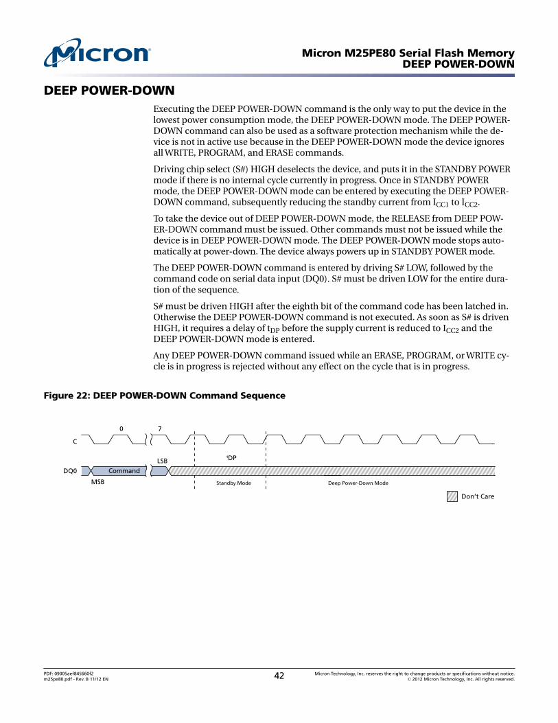
DEEP POWER-DOWNExecuting the DEEP POWER-DOWN command is the only way to put the device in thelowest power consumption mode, the DEEP POWER-DOWN mode. The DEEP POWER-DOWN command can also be used as a software protection mechanism while the de-vice is not in active use because in the DEEP POWER-DOWN mode the device ignoresall WRITE, PROGRAM, and ERASE commands.
Driving chip select (S#) HIGH deselects the device, and puts it in the STANDBY POWERmode if there is no internal cycle currently in progress. Once in STANDBY POWERmode, the DEEP POWER-DOWN mode can be entered by executing the DEEP POWER-DOWN command, subsequently reducing the standby current from ICC1 to ICC2.
To take the device out of DEEP POWER-DOWN mode, the RELEASE from DEEP POW-ER-DOWN command must be issued. Other commands must not be issued while thedevice is in DEEP POWER-DOWN mode. The DEEP POWER-DOWN mode stops auto-matically at power-down. The device always powers up in STANDBY POWER mode.
The DEEP POWER-DOWN command is entered by driving S# LOW, followed by thecommand code on serial data input (DQ0). S# must be driven LOW for the entire dura-tion of the sequence.
S# must be driven HIGH after the eighth bit of the command code has been latched in.Otherwise the DEEP POWER-DOWN command is not executed. As soon as S# is drivenHIGH, it requires a delay of tDP before the supply current is reduced to ICC2 and theDEEP POWER-DOWN mode is entered.
Any DEEP POWER-DOWN command issued while an ERASE, PROGRAM, or WRITE cy-cle is in progress is rejected without any effect on the cycle that is in progress.
Figure 22: DEEP POWER-DOWN Command Sequence
70
C
MSB
DQ0
LSBtDP
Command
Don’t Care
Deep Power-Down ModeStandby Mode
Micron M25PE80 Serial Flash MemoryDEEP POWER-DOWN
PDF: 09005aef845660f2m25pe80.pdf - Rev. B 11/12 EN 42 Micron Technology, Inc. reserves the right to change products or specifications without notice.
© 2012 Micron Technology, Inc. All rights reserved.
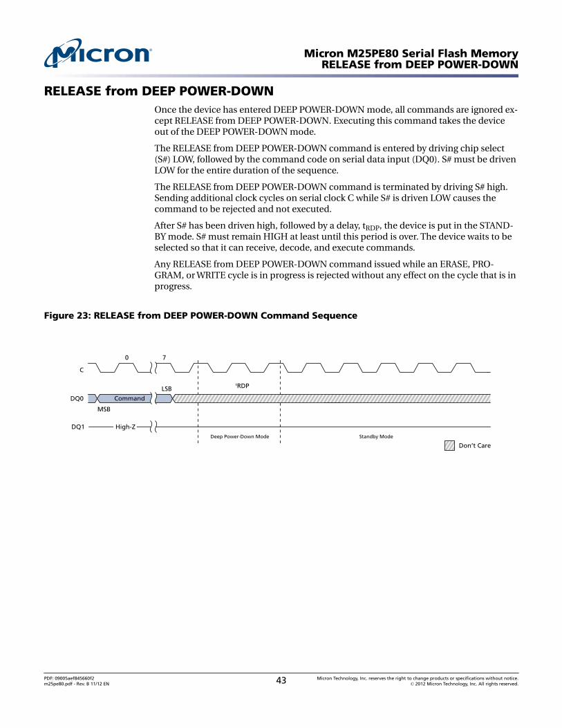
RELEASE from DEEP POWER-DOWNOnce the device has entered DEEP POWER-DOWN mode, all commands are ignored ex-cept RELEASE from DEEP POWER-DOWN. Executing this command takes the deviceout of the DEEP POWER-DOWN mode.
The RELEASE from DEEP POWER-DOWN command is entered by driving chip select(S#) LOW, followed by the command code on serial data input (DQ0). S# must be drivenLOW for the entire duration of the sequence.
The RELEASE from DEEP POWER-DOWN command is terminated by driving S# high.Sending additional clock cycles on serial clock C while S# is driven LOW causes thecommand to be rejected and not executed.
After S# has been driven high, followed by a delay, tRDP, the device is put in the STAND-BY mode. S# must remain HIGH at least until this period is over. The device waits to beselected so that it can receive, decode, and execute commands.
Any RELEASE from DEEP POWER-DOWN command issued while an ERASE, PRO-GRAM, or WRITE cycle is in progress is rejected without any effect on the cycle that is inprogress.
Figure 23: RELEASE from DEEP POWER-DOWN Command Sequence
High-ZDQ1
70
C
MSB
DQ0
LSBtRDP
Command
Don’t CareDeep Power-Down Mode Standby Mode
Micron M25PE80 Serial Flash MemoryRELEASE from DEEP POWER-DOWN
PDF: 09005aef845660f2m25pe80.pdf - Rev. B 11/12 EN 43 Micron Technology, Inc. reserves the right to change products or specifications without notice.
© 2012 Micron Technology, Inc. All rights reserved.
Power-Up and Power-DownAt power-up and power-down, the device must not be selected; that is, chip select (S#)must follow the voltage applied on VCC until VCC reaches the correct value:
• VCC(min) at power-up, and then for a further delay of tVSL
• VSS at power-down
A safe configuration is provided under the SPI modes heading.
To avoid data corruption and inadvertent write operations during power-up, a power-on-reset (POR) circuit is included. The logic inside the device is held reset while VCC isless than the POR threshold voltage, VWI – all operations are disabled, and the devicedoes not respond to any instruction. Moreover, the device ignores the following instruc-tions until a time delay of tPUW has elapsed after the moment that VCC rises above theVWI threshold:
• WRITE ENABLE• PAGE WRITE• PAGE PROGRAM• PAGE ERASE• SECTOR ERASE
However, the correct operation of the device is not guaranteed if, by this time, VCC is stillbelow VCC(min). No WRITE, PROGRAM, or ERASE instruction should be sent until:
• tPUW after VCC has passed the VWI threshold• tVSL after VCC has passed the VCC(min) level
If the time, tVSL, has elapsed, after VCC rises above VCC(min), the device can be selectedfor READ instructions even if the tPUW delay has not yet fully elapsed.
As an extra precaution, the RESET# signal could be driven LOW for the entire durationof the power-up and power-down phases.
Micron M25PE80 Serial Flash MemoryPower-Up and Power-Down
PDF: 09005aef845660f2m25pe80.pdf - Rev. B 11/12 EN 44 Micron Technology, Inc. reserves the right to change products or specifications without notice.
© 2012 Micron Technology, Inc. All rights reserved.
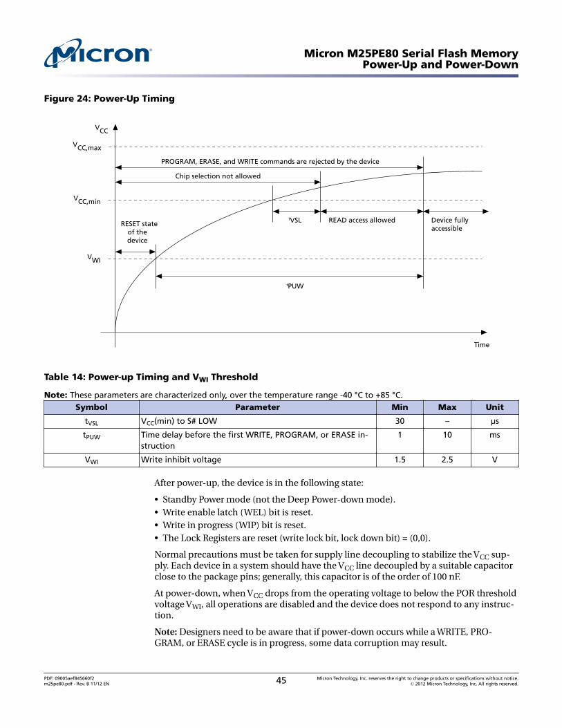
Figure 24: Power-Up Timing
VCC
VCC,min
VWI
RESET stateof thedevice
Chip selection not allowed
PROGRAM, ERASE, and WRITE commands are rejected by the device
tVSL
tPUW
Time
READ access allowed Device fullyaccessible
VCC,max
Table 14: Power-up Timing and VWI Threshold
Note: These parameters are characterized only, over the temperature range -40 °C to +85 °C.Symbol Parameter Min Max Unit
tVSL VCC(min) to S# LOW 30 – µs
tPUW Time delay before the first WRITE, PROGRAM, or ERASE in-struction
1 10 ms
VWI Write inhibit voltage 1.5 2.5 V
After power-up, the device is in the following state:
• Standby Power mode (not the Deep Power-down mode).• Write enable latch (WEL) bit is reset.• Write in progress (WIP) bit is reset.• The Lock Registers are reset (write lock bit, lock down bit) = (0,0).
Normal precautions must be taken for supply line decoupling to stabilize the VCC sup-ply. Each device in a system should have the VCC line decoupled by a suitable capacitorclose to the package pins; generally, this capacitor is of the order of 100 nF.
At power-down, when VCC drops from the operating voltage to below the POR thresholdvoltage VWI, all operations are disabled and the device does not respond to any instruc-tion.
Note: Designers need to be aware that if power-down occurs while a WRITE, PRO-GRAM, or ERASE cycle is in progress, some data corruption may result.
Micron M25PE80 Serial Flash MemoryPower-Up and Power-Down
PDF: 09005aef845660f2m25pe80.pdf - Rev. B 11/12 EN 45 Micron Technology, Inc. reserves the right to change products or specifications without notice.
© 2012 Micron Technology, Inc. All rights reserved.
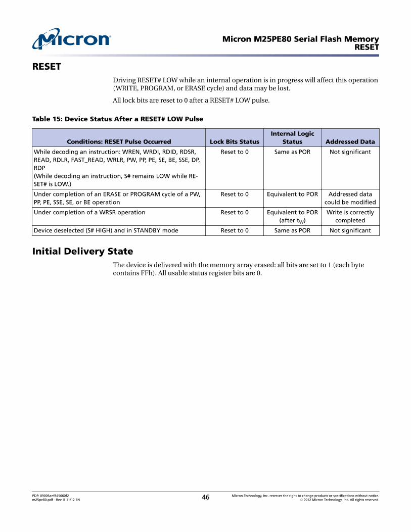
RESETDriving RESET# LOW while an internal operation is in progress will affect this operation(WRITE, PROGRAM, or ERASE cycle) and data may be lost.
All lock bits are reset to 0 after a RESET# LOW pulse.
Table 15: Device Status After a RESET# LOW Pulse
Conditions: RESET Pulse Occurred Lock Bits StatusInternal Logic
Status Addressed Data
While decoding an instruction: WREN, WRDI, RDID, RDSR,READ, RDLR, FAST_READ, WRLR, PW, PP, PE, SE, BE, SSE, DP,RDP(While decoding an instruction, S# remains LOW while RE-SET# is LOW.)
Reset to 0 Same as POR Not significant
Under completion of an ERASE or PROGRAM cycle of a PW,PP, PE, SSE, SE, or BE operation
Reset to 0 Equivalent to POR Addressed datacould be modified
Under completion of a WRSR operation Reset to 0 Equivalent to POR(after tW)
Write is correctlycompleted
Device deselected (S# HIGH) and in STANDBY mode Reset to 0 Same as POR Not significant
Initial Delivery StateThe device is delivered with the memory array erased: all bits are set to 1 (each bytecontains FFh). All usable status register bits are 0.
Micron M25PE80 Serial Flash MemoryRESET
PDF: 09005aef845660f2m25pe80.pdf - Rev. B 11/12 EN 46 Micron Technology, Inc. reserves the right to change products or specifications without notice.
© 2012 Micron Technology, Inc. All rights reserved.
Maximum Ratings and Operating ConditionsCAUTION: Stressing the device beyond the absolute maximum ratings may cause per-manent damage to the device. These are stress ratings only and operation of the devicebeyond any specification or condition in the operating sections of this datasheet is notrecommended. Exposure to absolute maximum rating conditions for extended periodsmay affect device reliability.
Table 16: Absolute Maximum Ratings
Symbol Parameter Min Max Units Notes
TSTG Storage temperature –65 150 °C
TLEAD Lead temperature during soldering See note °C 1
VIO Input and output voltage (with respect toground)
–0.6 VCC+0.6 V
VCC Supply voltage –0.6 4.0 V
VESD Electrostatic discharge voltage (Human Bodymodel)
–2000 2000 V 2
Notes: 1. The TLEAD signal is compliant with JEDEC Std J-STD-020C (for small body, Sn-Pb or Pb as-sembly), the Micron RoHS compliant 7191395 specification, and the European directiveon Restrictions on Hazardous Substances (RoHS) 2002/95/EU.
2. The VESD signal: JEDEC Std JESD22-A114A (C1 = 100 pF, R1 = 1500 Ω, R2 = 500 Ω).
Table 17: Operating Conditions
Symbol Parameter Min Max Unit
VCC Supply voltage 2.7 3.6 V
TA Ambient operating temperature –40 85 °C
Micron M25PE80 Serial Flash MemoryMaximum Ratings and Operating Conditions
PDF: 09005aef845660f2m25pe80.pdf - Rev. B 11/12 EN 47 Micron Technology, Inc. reserves the right to change products or specifications without notice.
© 2012 Micron Technology, Inc. All rights reserved.
DC Parameters
Table 18: DC Characteristics
Symbol Parameter
Test Conditions(in addition to those listed in Oper-
ating Conditions table) Min Max Units
ILI Input leakage current – – ±2 µA
ILO Output leakage current – – ±2 µA
ICC1 Standby current (Standby and Re-set modes)
S# = VCC, VIN = VSS or VCC – 50 µA
ICC2 Deep power-down current S# = VCC, VIN = VSS or VCC – 10 µA
ICC3 Operating current (FAST_READ) C = 0.1VCC / 0.9VCC at 50 MHz, DQ1 =open
– 8 mA
C = 0.1VCC / 0.9VCC at 33 MHz, DQ1 =open
– 6 mA
ICC4 Operating current(PAGE WRITE)
S# = VCC – 15 mA
ICC5 Operating current(SECTOR ERASE)
S# = VCC – 15 mA
VIL Input Low Voltage -0.5 0.3VCC V
VIH Input High Voltage 0.7VCC VCC+0.4 V
VOL Output Low Voltage IOL = 1.6mA 0.4 V
VOH Output High Voltage IOH = -100 µA VCC-0.2 V
Table 19: DC Characteristics 75 MHz Operation
Symbol Parameter
Test Conditons(in addition to those listed in Oper-
ating Conditions table) Min Max Units
ILI Input leakage current – – ±2 µA
ILO Output leakage current – – ±2 µA
ICC1 Standby current (Standby and Re-set modes)
S# = VCC, VIN = VSS or VCC – 50 µA
ICC2 Deep power-down current S# = VCC, VIN = VSS or VCC – 10 µA
ICC3 Operating current (FAST_READ) C = 0.1VCC / 0.9VCC at 33 MHz, DQ1 =open
– 4 mA
C = 0.1VCC / 0.9VCC at 75 MHz, DQ1 =open
– 12 mA
ICC4 Operating current(PAGE WRITE)
S# = VCC – 15 mA
ICC5 Operating current(SECTOR ERASE)
S# = VCC – 15 mA
VIL Input Low Voltage -0.5 0.3VCC V
VIH Input High Voltage 0.7VCC VCC+0.4 V
Micron M25PE80 Serial Flash MemoryDC Parameters
PDF: 09005aef845660f2m25pe80.pdf - Rev. B 11/12 EN 48 Micron Technology, Inc. reserves the right to change products or specifications without notice.
© 2012 Micron Technology, Inc. All rights reserved.
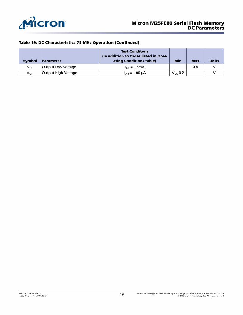
Table 19: DC Characteristics 75 MHz Operation (Continued)
Symbol Parameter
Test Conditons(in addition to those listed in Oper-
ating Conditions table) Min Max Units
VOL Output Low Voltage IOL = 1.6mA 0.4 V
VOH Output High Voltage IOH = -100 µA VCC-0.2 V
Micron M25PE80 Serial Flash MemoryDC Parameters
PDF: 09005aef845660f2m25pe80.pdf - Rev. B 11/12 EN 49 Micron Technology, Inc. reserves the right to change products or specifications without notice.
© 2012 Micron Technology, Inc. All rights reserved.
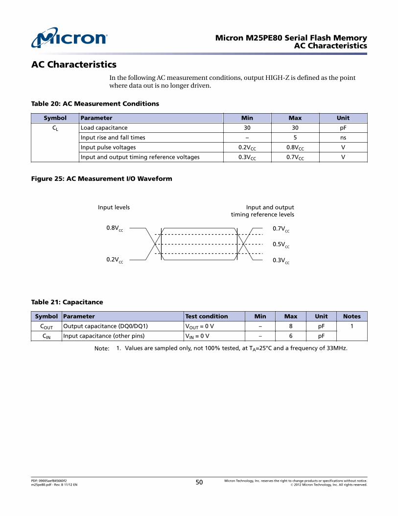
AC CharacteristicsIn the following AC measurement conditions, output HIGH-Z is defined as the pointwhere data out is no longer driven.
Table 20: AC Measurement Conditions
Symbol Parameter Min Max Unit
CL Load capacitance 30 30 pF
Input rise and fall times – 5 ns
Input pulse voltages 0.2VCC 0.8VCC V
Input and output timing reference voltages 0.3VCC 0.7VCC V
Figure 25: AC Measurement I/O Waveform
Input and outputtiming reference levels
Input levels
0.8VCC
0.2VCC
0.7VCC
0.3VCC
0.5VCC
Table 21: Capacitance
Symbol Parameter Test condition Min Max Unit Notes
COUT Output capacitance (DQ0/DQ1) VOUT = 0 V – 8 pF 1
CIN Input capacitance (other pins) VIN = 0 V – 6 pF
Note: 1. Values are sampled only, not 100% tested, at TA=25°C and a frequency of 33MHz.
Micron M25PE80 Serial Flash MemoryAC Characteristics
PDF: 09005aef845660f2m25pe80.pdf - Rev. B 11/12 EN 50 Micron Technology, Inc. reserves the right to change products or specifications without notice.
© 2012 Micron Technology, Inc. All rights reserved.
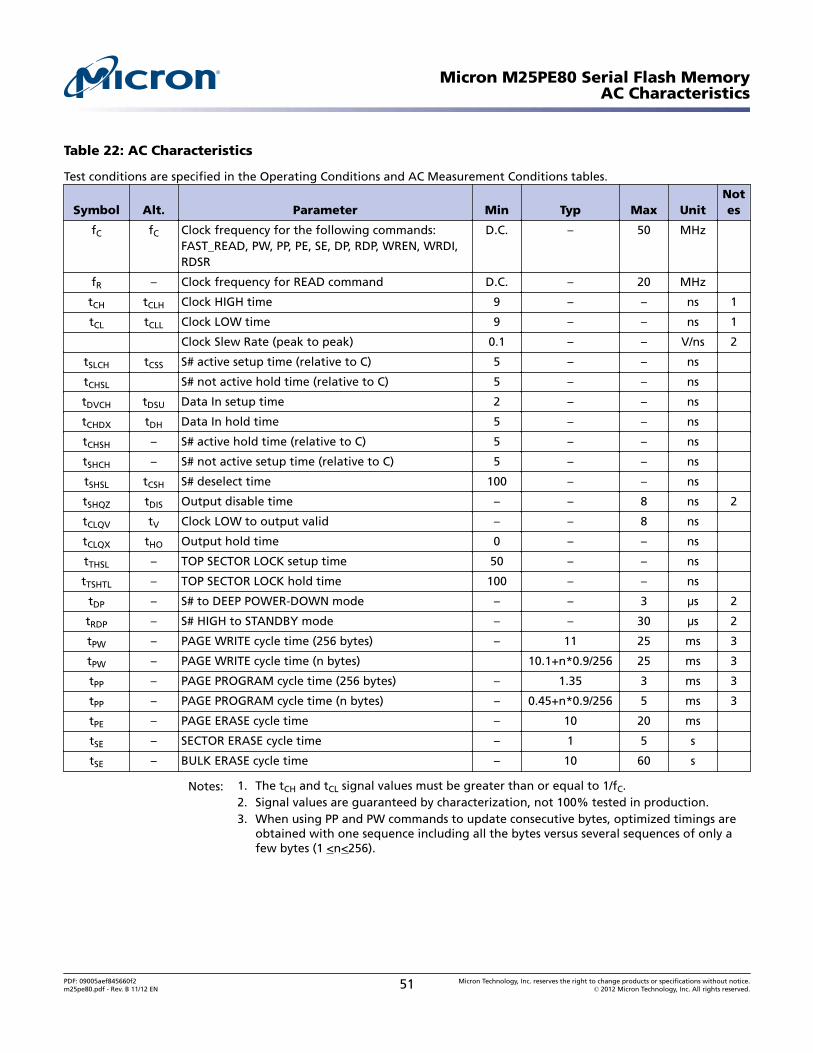
Table 22: AC Characteristics
Test conditions are specified in the Operating Conditions and AC Measurement Conditions tables.
Symbol Alt. Parameter Min Typ Max UnitNotes
fC fC Clock frequency for the following commands:FAST_READ, PW, PP, PE, SE, DP, RDP, WREN, WRDI,RDSR
D.C. – 50 MHz
fR – Clock frequency for READ command D.C. – 20 MHz
tCH tCLH Clock HIGH time 9 – – ns 1
tCL tCLL Clock LOW time 9 – – ns 1
Clock Slew Rate (peak to peak) 0.1 – – V/ns 2
tSLCH tCSS S# active setup time (relative to C) 5 – – ns
tCHSL S# not active hold time (relative to C) 5 – – ns
tDVCH tDSU Data In setup time 2 – – ns
tCHDX tDH Data In hold time 5 – – ns
tCHSH – S# active hold time (relative to C) 5 – – ns
tSHCH – S# not active setup time (relative to C) 5 – – ns
tSHSL tCSH S# deselect time 100 – – ns
tSHQZ tDIS Output disable time – – 8 ns 2
tCLQV tV Clock LOW to output valid – – 8 ns
tCLQX tHO Output hold time 0 – – ns
tTHSL – TOP SECTOR LOCK setup time 50 – – ns
tTSHTL – TOP SECTOR LOCK hold time 100 – – ns
tDP – S# to DEEP POWER-DOWN mode – – 3 μs 2
tRDP – S# HIGH to STANDBY mode – – 30 μs 2
tPW – PAGE WRITE cycle time (256 bytes) – 11 25 ms 3
tPW – PAGE WRITE cycle time (n bytes) 10.1+n*0.9/256 25 ms 3
tPP – PAGE PROGRAM cycle time (256 bytes) – 1.35 3 ms 3
tPP – PAGE PROGRAM cycle time (n bytes) – 0.45+n*0.9/256 5 ms 3
tPE – PAGE ERASE cycle time – 10 20 ms
tSE – SECTOR ERASE cycle time – 1 5 s
tSE – BULK ERASE cycle time – 10 60 s
Notes: 1. The tCH and tCL signal values must be greater than or equal to 1/fC.2. Signal values are guaranteed by characterization, not 100% tested in production.3. When using PP and PW commands to update consecutive bytes, optimized timings are
obtained with one sequence including all the bytes versus several sequences of only afew bytes (1 <n<256).
Micron M25PE80 Serial Flash MemoryAC Characteristics
PDF: 09005aef845660f2m25pe80.pdf - Rev. B 11/12 EN 51 Micron Technology, Inc. reserves the right to change products or specifications without notice.
© 2012 Micron Technology, Inc. All rights reserved.
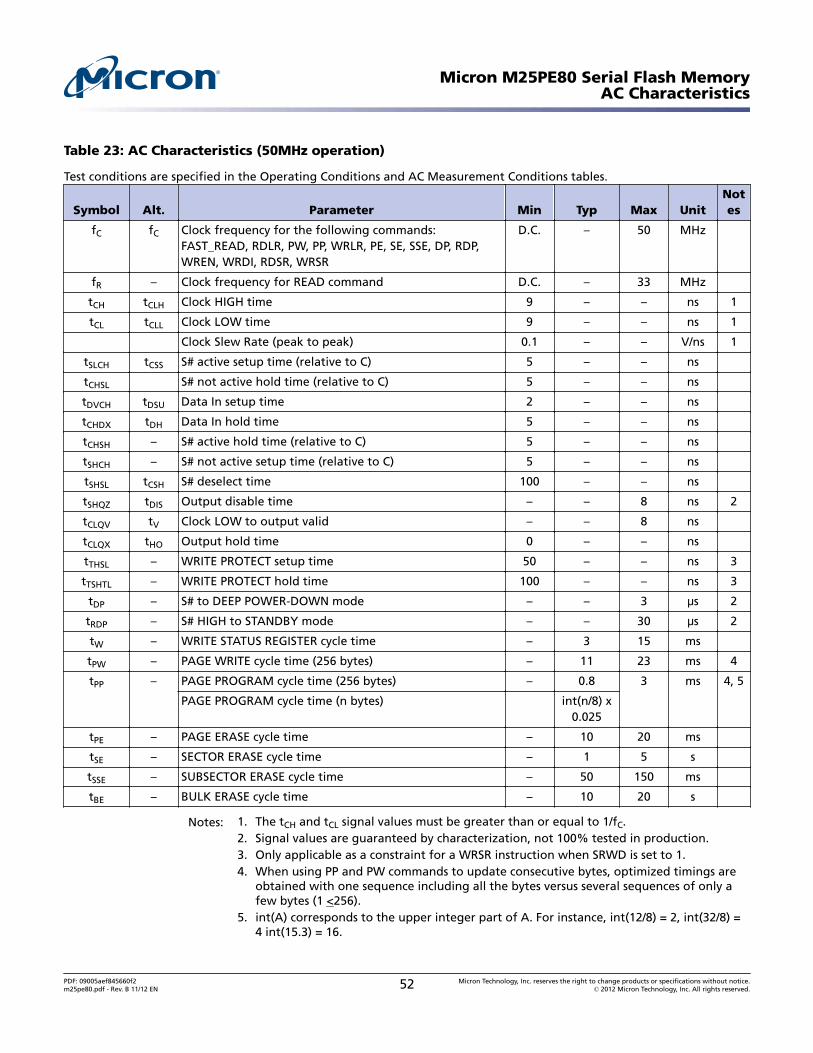
Table 23: AC Characteristics (50MHz operation)
Test conditions are specified in the Operating Conditions and AC Measurement Conditions tables.
Symbol Alt. Parameter Min Typ Max UnitNotes
fC fC Clock frequency for the following commands:FAST_READ, RDLR, PW, PP, WRLR, PE, SE, SSE, DP, RDP,WREN, WRDI, RDSR, WRSR
D.C. – 50 MHz
fR – Clock frequency for READ command D.C. – 33 MHz
tCH tCLH Clock HIGH time 9 – – ns 1
tCL tCLL Clock LOW time 9 – – ns 1
Clock Slew Rate (peak to peak) 0.1 – – V/ns 1
tSLCH tCSS S# active setup time (relative to C) 5 – – ns
tCHSL S# not active hold time (relative to C) 5 – – ns
tDVCH tDSU Data In setup time 2 – – ns
tCHDX tDH Data In hold time 5 – – ns
tCHSH – S# active hold time (relative to C) 5 – – ns
tSHCH – S# not active setup time (relative to C) 5 – – ns
tSHSL tCSH S# deselect time 100 – – ns
tSHQZ tDIS Output disable time – – 8 ns 2
tCLQV tV Clock LOW to output valid – – 8 ns
tCLQX tHO Output hold time 0 – – ns
tTHSL – WRITE PROTECT setup time 50 – – ns 3
tTSHTL – WRITE PROTECT hold time 100 – – ns 3
tDP – S# to DEEP POWER-DOWN mode – – 3 μs 2
tRDP – S# HIGH to STANDBY mode – – 30 μs 2
tW – WRITE STATUS REGISTER cycle time – 3 15 ms
tPW – PAGE WRITE cycle time (256 bytes) – 11 23 ms 4
tPP – PAGE PROGRAM cycle time (256 bytes) – 0.8 3 ms 4, 5
PAGE PROGRAM cycle time (n bytes) int(n/8) x0.025
tPE – PAGE ERASE cycle time – 10 20 ms
tSE – SECTOR ERASE cycle time – 1 5 s
tSSE – SUBSECTOR ERASE cycle time – 50 150 ms
tBE – BULK ERASE cycle time – 10 20 s
Notes: 1. The tCH and tCL signal values must be greater than or equal to 1/fC.2. Signal values are guaranteed by characterization, not 100% tested in production.3. Only applicable as a constraint for a WRSR instruction when SRWD is set to 1.4. When using PP and PW commands to update consecutive bytes, optimized timings are
obtained with one sequence including all the bytes versus several sequences of only afew bytes (1 <256).
5. int(A) corresponds to the upper integer part of A. For instance, int(12/8) = 2, int(32/8) =4 int(15.3) = 16.
Micron M25PE80 Serial Flash MemoryAC Characteristics
PDF: 09005aef845660f2m25pe80.pdf - Rev. B 11/12 EN 52 Micron Technology, Inc. reserves the right to change products or specifications without notice.
© 2012 Micron Technology, Inc. All rights reserved.
Table 24: AC Specifications (75 MHz operation)
Test conditions are specified in the Operating Conditions and AC Measurement Conditions tables.
Symbol Alt. Parameter Min Typ Max UnitNotes
fC fC Clock frequency for the following commands:FAST_READ, RDLR, PW, PP, WRLR, PE, SE, SSE, DP, RDP,WREN, WRDI, RDSR, WRSR
D.C. – 75 MHz
fR – Clock frequency for READ command D.C. – 33 MHz
tCH tCLH Clock HIGH time 6 – – ns 1
tCL tCLL Clock LOW time 6 – – ns 1
Clock Slew Rate (peak to peak) 0.1 – – V/ns 1
tSLCH tCSS S# active setup time (relative to C) 5 – – ns
tCHSL S# not active hold time (relative to C) 5 – – ns
tDVCH tDSU Data In setup time 2 – – ns
tCHDX tDH Data In hold time 5 – – ns
tCHSH – S# active hold time (relative to C) 5 – – ns
tSHCH – S# not active setup time (relative to C) 5 – – ns
tSHSL tCSH S# deselect time 100 – – ns
tSHQZ tDIS Output disable time – – 8 ns 2
tCLQV tV Clock LOW to output valid under 30pF/10pF – – 8/6 ns
tCLQX tHO Output hold time 0 – – ns
tWHSL – WRITE PROTECT setup time 20 – – ns 3
tSHWL – WRITE PROTECT hold time 100 – – ns 3
tDP – S# to DEEP POWER-DOWN mode – – 3 μs 2
tRDP – S# HIGH to STANDBY mode – – 30 μs 2
tW – WRITE STATUS REGISTER cycle time 3 15 ms
tPW – PAGE WRITE cycle time (256 bytes) – 11 23 ms
tPP – PAGE PROGRAM cycle time (256 bytes) – 0.8 3 ms 4
tPP – PAGE PROGRAM cycle time (n bytes) – int(n/8) x0.025
3 ms 4, 5
tPE – PAGE ERASE cycle time – 10 20 ms
tSE – SECTOR ERASE cycle time – 1 5 s
tSSE – SUBSECTOR ERASE cycle time – 50 150 ms
tBE – BULK ERASE cycle time – 10 20 s
Notes: 1. The tCH and tCL signal values must be greater than or equal to 1/fC.2. Signal values are guaranteed by characterization, not 100% tested in production.3. Only applicable as a constraint for a WRSR instruction when SRWD is set to 1.4. When using PP and PW commands to update consecutive bytes, optimized timings are
obtained with one sequence including all the bytes versus several sequences of only afew bytes (1 <n<256).
5. int(A) corresponds to the upper integer part of A. For example, int(12/8) = 2, int(32/8) =4, int(15.3) = 16.
Micron M25PE80 Serial Flash MemoryAC Characteristics
PDF: 09005aef845660f2m25pe80.pdf - Rev. B 11/12 EN 53 Micron Technology, Inc. reserves the right to change products or specifications without notice.
© 2012 Micron Technology, Inc. All rights reserved.
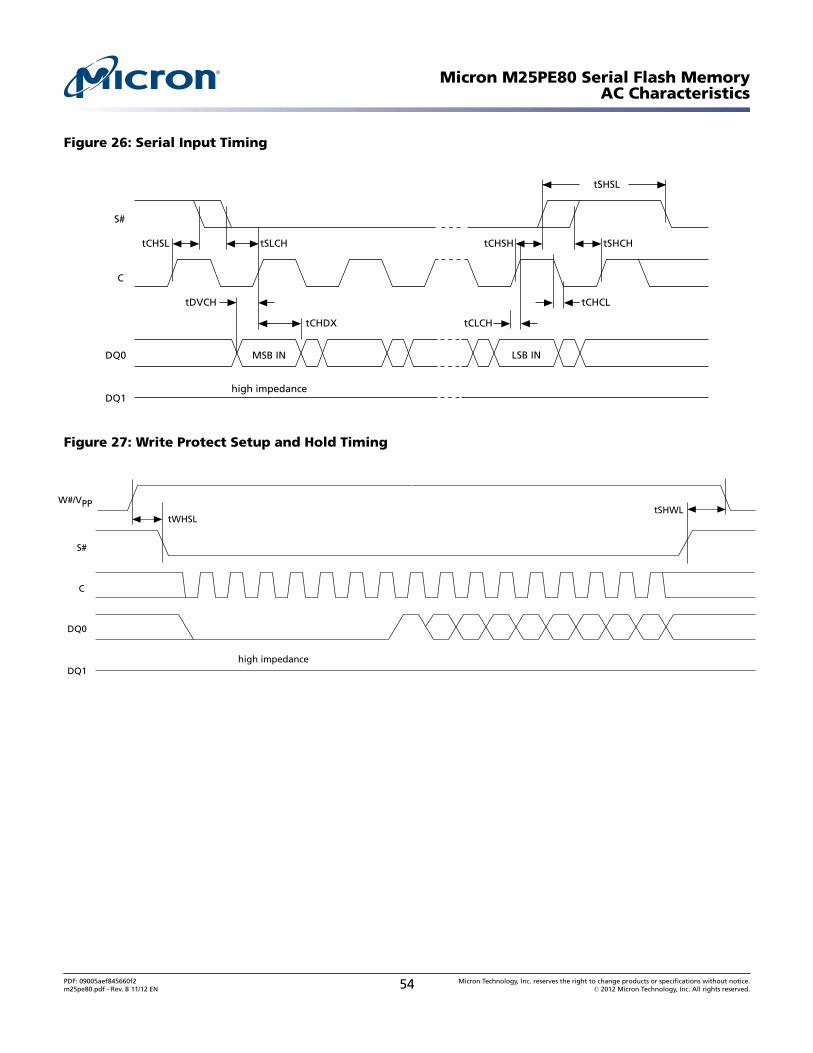
Figure 26: Serial Input Timing
C
DQ0
S#
MSB IN
DQ1
tDVCH
high impedance
LSB IN
tSLCH
tCHDX
tCHCL
tCLCH
tSHCH
tSHSL
tCHSHtCHSL
Figure 27: Write Protect Setup and Hold Timing
C
DQ0
S#
DQ1high impedance
W#/VPP
tWHSLtSHWL
Micron M25PE80 Serial Flash MemoryAC Characteristics
PDF: 09005aef845660f2m25pe80.pdf - Rev. B 11/12 EN 54 Micron Technology, Inc. reserves the right to change products or specifications without notice.
© 2012 Micron Technology, Inc. All rights reserved.
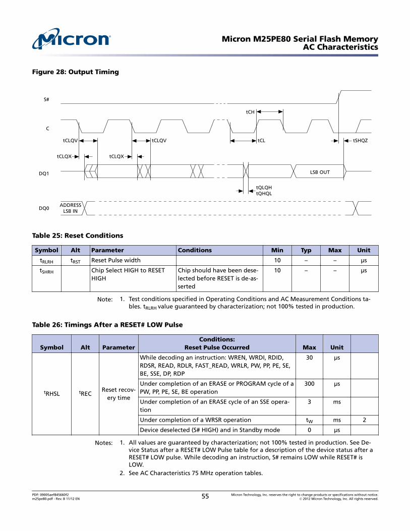
Figure 28: Output Timing
C
DQ1
S#
LSB OUT
DQ0ADDRESS
LSB IN
tSHQZ
tCH
tCL
tQLQHtQHQL
tCLQX
tCLQV
tCLQX
tCLQV
Table 25: Reset Conditions
Symbol Alt Parameter Conditions Min Typ Max Unit
tRLRH tRST Reset Pulse width 10 – – µs
tSHRH Chip Select HIGH to RESETHIGH
Chip should have been dese-lected before RESET is de-as-serted
10 – – µs
Note: 1. Test conditions specified in Operating Conditions and AC Measurement Conditions ta-bles. tRLRH value guaranteed by characterization; not 100% tested in production.
Table 26: Timings After a RESET# LOW Pulse
Symbol Alt ParameterConditions:
Reset Pulse Occurred Max Unit
tRHSL tRECReset recov-
ery time
While decoding an instruction: WREN, WRDI, RDID,RDSR, READ, RDLR, FAST_READ, WRLR, PW, PP, PE, SE,BE, SSE, DP, RDP
30 µs
Under completion of an ERASE or PROGRAM cycle of aPW, PP, PE, SE, BE operation
300 µs
Under completion of an ERASE cycle of an SSE opera-tion
3 ms
Under completion of a WRSR operation tW ms 2
Device deselected (S# HIGH) and in Standby mode 0 µs
Notes: 1. All values are guaranteed by characterization; not 100% tested in production. See De-vice Status after a RESET# LOW Pulse table for a description of the device status after aRESET# LOW pulse. While decoding an instruction, S# remains LOW while RESET# isLOW.
2. See AC Characteristics 75 MHz operation tables.
Micron M25PE80 Serial Flash MemoryAC Characteristics
PDF: 09005aef845660f2m25pe80.pdf - Rev. B 11/12 EN 55 Micron Technology, Inc. reserves the right to change products or specifications without notice.
© 2012 Micron Technology, Inc. All rights reserved.
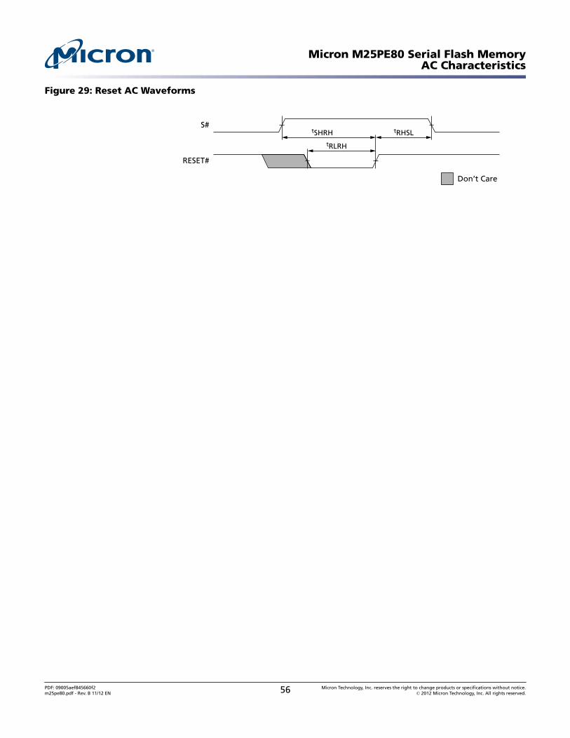
Figure 29: Reset AC Waveforms
tSHRHtRLRH
tRHSLS#
RESET#
Don’t Care
Micron M25PE80 Serial Flash MemoryAC Characteristics
PDF: 09005aef845660f2m25pe80.pdf - Rev. B 11/12 EN 56 Micron Technology, Inc. reserves the right to change products or specifications without notice.
© 2012 Micron Technology, Inc. All rights reserved.
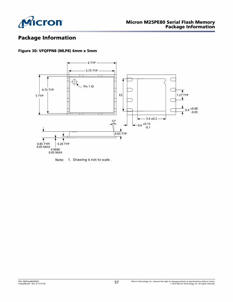
Package Information
Figure 30: VFQFPN8 (MLP8) 6mm x 5mm
6 TYP
5 TYP
0.65 TYP
12°
0.85 TYP/0.05 MAX
0.20 TYP
0 MIN/0.05 MAX
4.75 TYPPin 1 ID
5.75 TYP
1.27 TYPE2
3.4 ±0.2
0.6 +0.15-0.1
0.4 +0.08-0.05
Note: 1. Drawing is not to scale.
Micron M25PE80 Serial Flash MemoryPackage Information
PDF: 09005aef845660f2m25pe80.pdf - Rev. B 11/12 EN 57 Micron Technology, Inc. reserves the right to change products or specifications without notice.
© 2012 Micron Technology, Inc. All rights reserved.
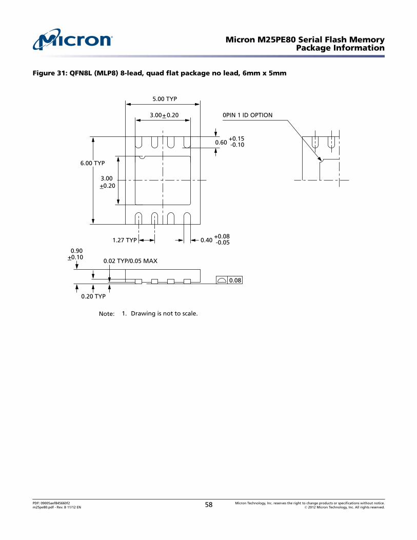
Figure 31: QFN8L (MLP8) 8-lead, quad flat package no lead, 6mm x 5mm
0.08
3.00 +0.20
3.00 +0.20
1.27 TYP
5.00 TYP
0.90
0.20 TYP
0.02 TYP/0.05 MAX
0PIN 1 ID OPTION
+0.10
0.60 +0.15-0.10
0.40 +0.08-0.05
6.00 TYP
Note: 1. Drawing is not to scale.
Micron M25PE80 Serial Flash MemoryPackage Information
PDF: 09005aef845660f2m25pe80.pdf - Rev. B 11/12 EN 58 Micron Technology, Inc. reserves the right to change products or specifications without notice.
© 2012 Micron Technology, Inc. All rights reserved.
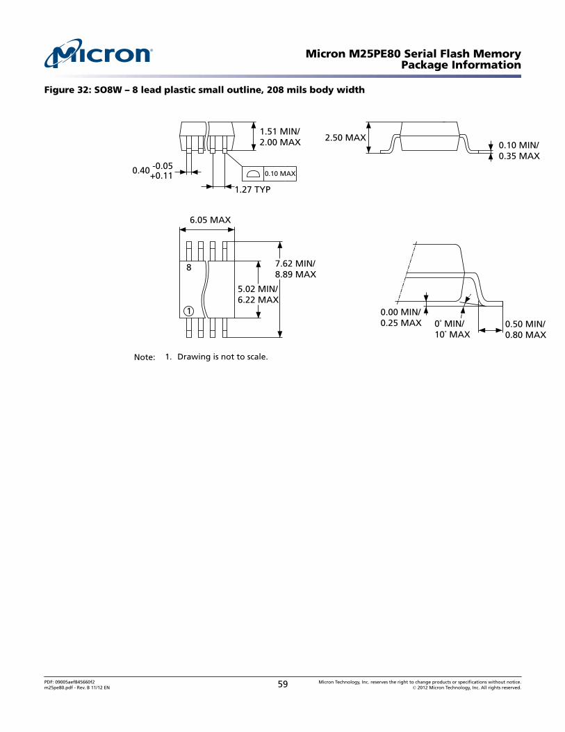
Figure 32: SO8W – 8 lead plastic small outline, 208 mils body width
8
1 0.00 MIN/0.25 MAX
1.51 MIN/2.00 MAX
5.02 MIN/6.22 MAX
7.62 MIN/8.89 MAX
0º MIN/10° MAX
0.10 MIN/0.35 MAX
0.50 MIN/0.80 MAX
2.50 MAX
6.05 MAX
1.27 TYP
0.40 -0.05+0.11 0.10 MAX
Note: 1. Drawing is not to scale.
Micron M25PE80 Serial Flash MemoryPackage Information
PDF: 09005aef845660f2m25pe80.pdf - Rev. B 11/12 EN 59 Micron Technology, Inc. reserves the right to change products or specifications without notice.
© 2012 Micron Technology, Inc. All rights reserved.
Device Ordering InformationFor a list of available options (speed, packaging, and so on), for further information onany aspect of this device, or when ordering parts operating at 75 MHz, contact yournearest representative.
Table 27: Standard Part Number Information Scheme
Part NumberCategory Category Details Notes
Device type M25PE = Page-erasable serial Flash memory
Density 80 = 8Mb (1Mb x 8)
Operating voltage V = VCC = 2.7V to 3.6V
Package MW = SO8W (208 mils width)
MN = SO8N (150 mils width)
MP = VFQFPN8 6mm x 5mm (MLP8)
MS = QFN8L 6mm x 5mm (MLP8) 1
Device Grade 6 = Industrial temperature range: –40 °C to 85 °C. Device tested with standard test flow.
Packing Option – = Standard packing
T = Tape and reel packing
Plating technology P or G = RoHS compliant
Note: 1. Exposed pad of 3mm x 3mm.
Table 28: Automotive Part Number Information Scheme
Part NumberCategory Category Details
Device type M25PE = Page-erasable serial Flash memory
Density 80 = 8Mb (1Mb x 8)
Operating voltage V = VCC = 2.7V to 3.6V
Package MN = SO8N (150 mils width)
Device Grade 6 = Industrial temperature range: –40 °C to 85 °C. Device tested with standard test flow.
Packing Option – = Standard packing
T = Tape and reel packing
Plating technology P = RoHS compliant
Lithography B = 110nm, Fab 2 diffusion plant
blank = Industrial part (Refer to Standard Part Number Information Scheme)
Automotive grade A = Automotive grade –40 to 85 °C. Device tested with high reliability certified flow
blank = Standard –40 to 85 °C device (Refer to Standard Part Number Information Scheme)
Micron M25PE80 Serial Flash MemoryDevice Ordering Information
PDF: 09005aef845660f2m25pe80.pdf - Rev. B 11/12 EN 60 Micron Technology, Inc. reserves the right to change products or specifications without notice.
© 2012 Micron Technology, Inc. All rights reserved.
Revision History
Rev. B – 11/2012
• Removed T9HX process information• Added automotive grade part information
Rev. A – 09/2012
• Applied Micron branding.
8000 S. Federal Way, P.O. Box 6, Boise, ID 83707-0006, Tel: 208-368-3900www.micron.com/productsupport Customer Comment Line: 800-932-4992
Micron and the Micron logo are trademarks of Micron Technology, Inc.All other trademarks are the property of their respective owners.
This data sheet contains minimum and maximum limits specified over the power supply and temperature range set forth herein.Although considered final, these specifications are subject to change, as further product development and data characterization some-
times occur.
Micron M25PE80 Serial Flash MemoryRevision History
PDF: 09005aef845660f2m25pe80.pdf - Rev. B 11/12 EN 61 Micron Technology, Inc. reserves the right to change products or specifications without notice.
© 2012 Micron Technology, Inc. All rights reserved.