micro/nano engineering lab “mems (micro electro ... micro/nano engineering lab “mems (micro...
TRANSCRIPT

1
Micro/NanoEngineeringLab
“MEMS(MicroElectro-MechanicalSystems)”
2.674Sang-Gook Kim
1
• Labsections
• Labmanual(Module#1and#2)
• Labsafetytrainingcertificate,dueFeb.16,12PM.
• Readingsuggestions
– FeynmanLecture,“PlentyofRoomattheBottom”
– IntroMEMS
– Madou,M.J.(2002).FundamentalsofMicrofabrication. (2nded.).CRCPress
– C.Liu,FoundationsofMEMS,PrenticeHall,2006
2
2
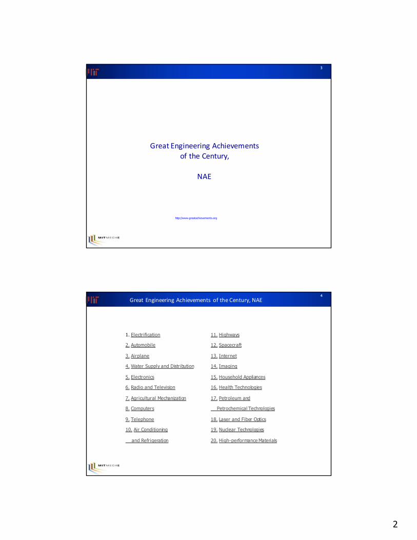
GreatEngineeringAchievementsoftheCentury,
NAE
http://www.greatachievements.org
3
GreatEngineeringAchievementsoftheCentury,NAE
1. Electrification 11. Highways
2. Automobile 12. Spacecraft
3. Airplane 13. Internet
4. Water Supply and Distribution 14. Imaging
5. Electronics 15. Household Appliances
6. Radio and Television 16. Health Technologies
7. Agricultural Mechanization 17. Petroleum and
8. Computers Petrochemical Technologies
9. Telephone 18. Laser and Fiber Optics
10. Air Conditioning 19. Nuclear Technologies
and Refrigeration 20. High-performance Materials
4

3
Nolimitinthescaleofintegration5
Electricalcircuits:top-downnanotechnology
www.intel.com/pressroom/kits/core2duo/index.htm
IBM's Early Computers (1950s), MIT Press.
First transistor made in 1947 by Shockley, Bardeen, and Brittain at Bell Labs.
Early integrated circuit from MIT. Edwin Hall, circa 1965.
6
SiliconValleyAMovie
This image has been removed due to copyright restrictions.Please see https://commons.wikimedia.org/wiki/File:Transistor_Count_and_Moore's_Law_-_2008_1024.png.
© MIT, Intel, and sources unknown. All rights reserved. This content is excluded from our Creative Commons license. For more information, see https://ocw.mit.edu/help/faq-fair-use.
This image has been removed due to copyright restrictions.Please see https://www.legitreviews.com/images/reviews/668/cores.jpg.

4
Segway
7
-pitch ✓-roll-yaw
InertialNavigationSystem8
-Rate grade, tactical grade, inertial grade-Bias drift (o/h)
)(2 vmFc ×−= ω
CoriolisAcceleration
These images are in the public domain.
Image courtesy of cpsc.gov.
This image has been removed due to copyright restrictions. Please see https://en.wikipedia. org/wiki/File:Centrale-inte rtielle _missile_S3_Musee_du_Bour get_P1010652.JPG.
This image has been removeddue to copyright restrictions.Please see https://www.invensense.com/wp-content/uploads/2015/01/rp-9-axis.png.
This image has been removed due to copyright restrictions. Please see https://idiotsecant. files.wordpress.com/2014/ 06/gyro.gif.
This image has been removed due to copyright restrictions.Please see http://volamar.ru/audio_video/foto/03/giroskopi/crs04_ring1.jpg.

5
HistoryofMEMS9
CombDriveDesigns10
Linear
Grating beamsFlexuresElectrostatic comb-drives
Barbastathis and Kim group, MIT
Image by MIT OpenCourseWare.
Bio MEMSRF MEMS
Si Gyro (Draper)DMD (TI)ADXL AccelerometerIR Imager (Honeywell)PolySi Comb Drive (Tang, Howe)PolySi Micromotor (Tai, Muller)
Metal Light Valve (RCA)
BJT TransistorIC
RGT (Nathanson et al)
Pressure Sensor (Honeywell)
Si as a Mechanical Material (Petersen)Si Pressure Sensor (Motorola)
SFBThermo-pneumatic Valve (Redwood)
SFB Pressure Sensor (NovaSensor)
LIGA
PolySi Beams (Howe, Muller)
XeF2/BrF3
DRIE !!
TMAH
KOH
Anodic BondingEDP
HNA
Metal Sacrificial Process (US Patent)
1990
2000
1980
1970
1960
1950
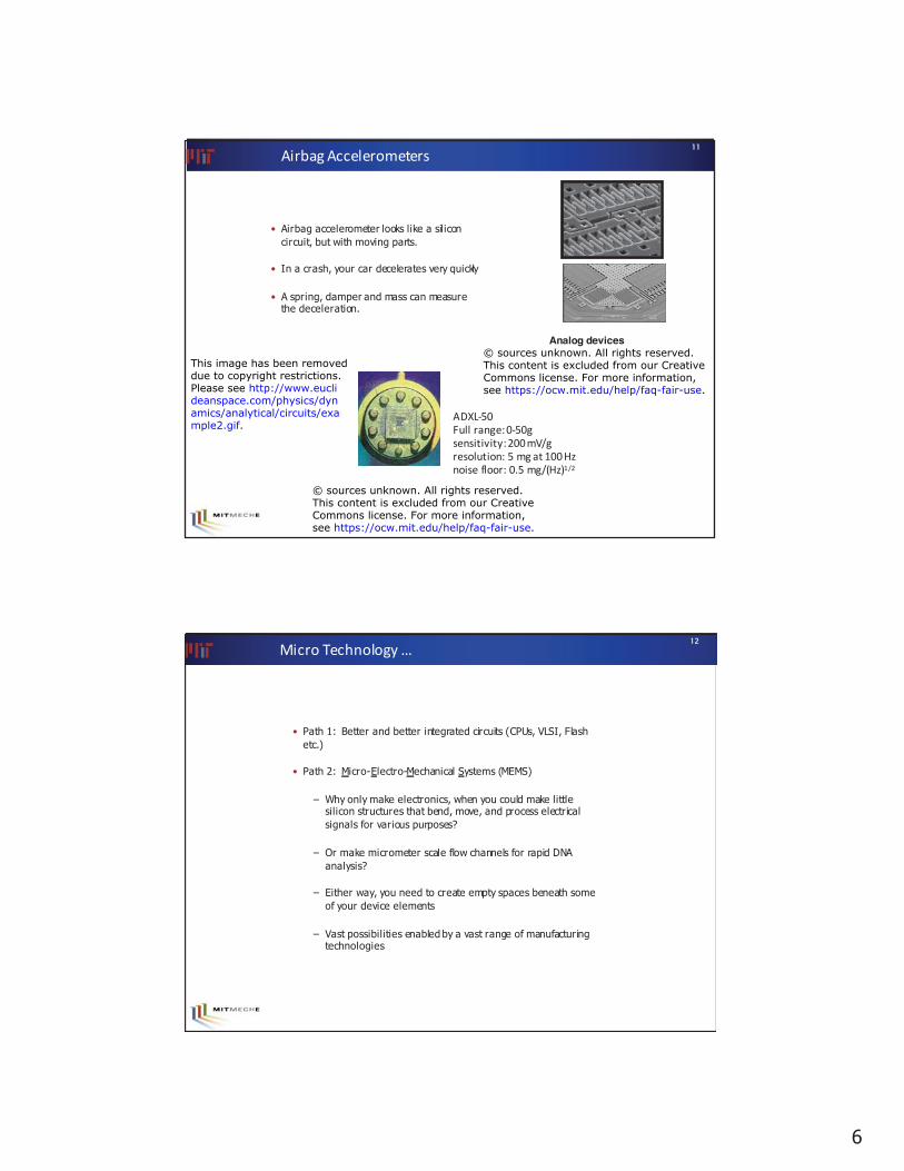
Analog devices
11
12
© sources unknown. All rights reserved. This content is excluded from our Creative Commons license. For more information, see https://ocw.mit.edu/help/faq-fair-use.
This image has been removeddue to copyright restrictions.Please see http://www.euclideanspace.com/physics/dynamics/analytical/circuits/example2.gif.
© sources unknown. All rights reserved. This content is excluded from our Creative Commons license. For more information, see https://ocw.mit.edu/help/faq-fair-use.

7
Whyshrink things?– scalinglaw 13
• Shock and impact• Scale and form factor• Load carrying capability
– Gravity• Surface/Volume
– Heat loss/generation– Cold blooded
Frog,WaterStrider,Gecko14
Mass/surface tension
Mass/surface areaSangbae Kim
This image has been removed due to copyright restrictions.Please see http://avenu.net/my/Neco/img/p13-1-05.jpg.
This image has been removed due to copyright restrictions.Please see https://commons.wikimedia.org/wiki/File:WeaverAntDefense.JPG.
This image has been removed due to copyright restrictions.Please see http://www.uksafari.com/jpeg3/pygmyshrew01.jpg.
Image courtesy of NASA.
© sources unknown. All rights reserved. This content is excluded from our Creative Commons license. For more information, see https://ocw.mit.edu/help/faq-fair-use.

115
μ
16
• barrier defines the walls of the chamberwhere the vaporbubble forms
nozzle
.
• refill channel lets freshink flow into chamber
• heater generates the vapor bubble in the ink
• nozzle is positionedMicroscopic view of a drop generator over resistor to form
(with nozzle plate removed) a drop of ink
Microscopic view under stroboscopic illumination• Up to 36 000 vapor bubble cycles per second
nononononnnononononoononononnnoonononnonoononnnooononnnooonoooooooonoooooooonooonnonoooozzzzzzzzzzzzzzzzzzzzzzzzzzzzzzzzzzzzzzzzzzzzzzzzzzzzzzzzzzzzzzzzzzzzzzzzz lelelelelelelelelllleleleleeeelllelelellleleleleleleeeleleleeeeeleeeeeeleeee
© HP. All rights reserved. This content is excluded from our Creative Commons license. For more information, see https://ocw.mit.edu/help/faq-fair-use.
sources unknown. All rights reserved. This content is excluded from our Creative Commons license. For more information, see https://ocw.mit.edu/help/faq-fair-use.
9
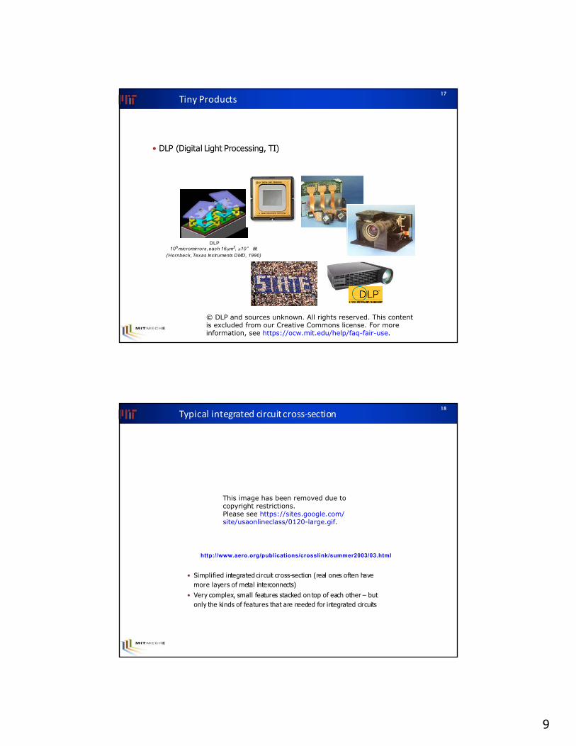
TinyProducts17
• DLP (Digital Light Processing, TI)
DLP106 micromirrors, each 16µm2, ±10° tilt
(Hornbeck, Texas Instruments DMD, 1990)
TM
Typicalintegratedcircuitcross-section
• Simplified integrated circuit cross-section (real ones often havemore layers of metal interconnects)
• Very complex, small features stacked on top of each other – but only the kinds of features that are needed for integrated circuits
http://www.aero.org/publications/crosslink/summer2003/03.html
18
© DLP and sources unknown. All rights reserved. This content is excluded from our Creative Commons license. For more information, see https://ocw.mit.edu/help/faq-fair-use.
This image has been removed due to copyright restrictions.Please see https://sites.google.com/site/usaonlineclass/0120-large.gif.

119
Deposition Lithography Etch
Wafers Devices
www.addisonengineering.com engr.calvin.edu
20
This image has been removeddue to copyright restrictions. This image has been removedPlease see http://abbiegregg due to copyright restrictions.com/images/silicon-wafers.png. Please see http://www.hilevel
com/waferth.JPG.
• Themostcommonwafersaresiliconwafers,asshownabove
• Otherwafers(glass,quartz,etc.)arealsoavailable
• Siliconwaferscomeinsizesfroma2” to12”
• Plain,unpatternedwafersarethenpatternedintoanarrayofsmall,repeatedstructurescalleddies
11
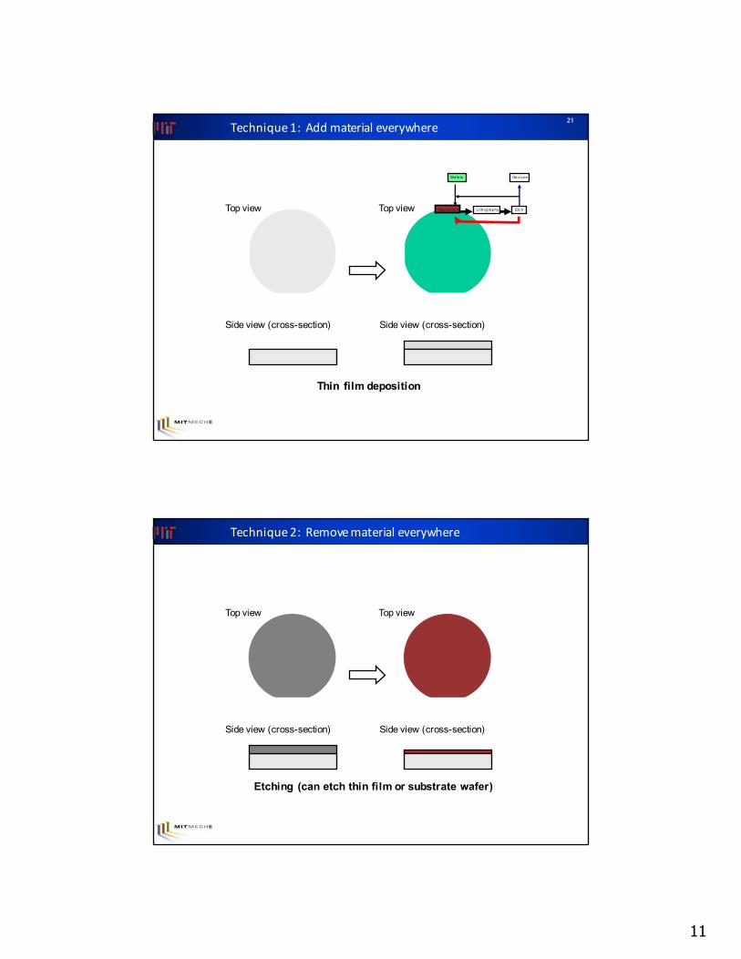
Technique1:Addmaterialeverywhere
Top view Top view
Side view (cross-section) Side view (cross-section)
Depos i tion Li thography Etc h
Wafers Dev ic es
21
Thin film deposition
Technique2:Removematerialeverywhere
Top view Top view
Side view (cross-section) Side view (cross-section)
Etching (can etch thin film or substrate wafer)
12
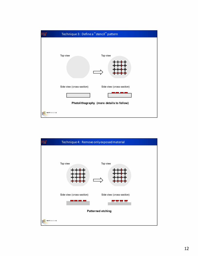
Technique3:Definea“stencil”pattern
Top view Top view
Side view (cross-section) Side view (cross-section)
Photolithography (more details to follow)
Technique4:Removeonlyexposedmaterial
Top view Top view
Side view (cross-section) Side view (cross-section)
Patterned etching

Top view
Side view (cross-section)Side view (cross-section)
Thin film lift-off
Real masks: patterned Transparency masks: patterns chrome on quartz or glass printed from a high resolution (expensive but high printer onto transparency film resolution) (cheap, fast, lower resolution)
www.toppan.co.jp
226
This image has been removeddue to copyright restrictionsPlease see http://www.toppan.co.jp/electronics/semicon/photo_mask/img/indx_pic_01.jpg.
© sources unknown. All rights reserved. This content is excluded from our Creative Commons license. For more information, see https://ocw.mit.edu/help/faq-fair-use.
This image has been removed due to copyright restrictions.Please see http://www.toppan.co.jp/electronics/semicon/photo_mask/img/indx_pic_01.jpg.

14
27
Lithography(Greek,“stone-writing”)
• Pattern Transfer– Application of photosensitive PR– Optical exposure to transfer image from mask to PR– Remove PR -à binary pattern transfer
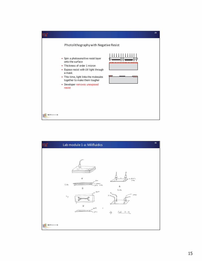
PhotolithographywithPositiveResist
• Spin a photosensitive resist layeronto the wafer surface
• Photoresist is a few micrometersthick
• Expose resist with UV light through a photolithographic mask; whereverthe light hits it, the resist moleculesget chopped up
• Developer removes exposed resist• Forms a stencil that determines
which parts of the surface areaffected by the next process
28
Image by MIT OpenCourseWare.
TOP VIEW
CROSS SECTION
Photosensitive materials properties change only where exposed to radiation
RadiationMask
PhotosensitivematerialSubstrate
29
30

16
Lab#131
Mixinginflowingsystems- Péclet number
• Péclet number: Compares transport due toadvection to transport due to diffusion
Ltadv U W
W 2 Ltdiff ~ D
D: difision Coeff.
timescale for diffusion across channel width W 2 /D LU W 2 W 2⎛ ⎞ ⎛ ⎞~ = ⎜ ⎟ = Pe⎜ ⎟
imescale for advection along channel length L /U D ⎝ L ⎠ ⎝ L ⎠
~ U
t
32

3
λ
33
Table 1: Wavelength "Generations"Intel Road Map
Year Node Lithography1981 2000nm i/g-line Steppers1984 1500nm i/g-line Steppers1987 1000nm i/g-line Steppers1990 800nm i/g-line Steppers1993 500nm i/g-line Steppers1995 350nm i-line -> DUV1997 250nm DUV1999 180nm DUV2001 130nm DUV2003 90nm 193nm2005 65nm 193nm -> 157nm2007 45nm 157nm -> EUV2009 32nm and below EUV, X-ray
n193 nm immersiolithography
334

MIT OpenCourseWarehttps://ocw.mit.edu
2.674 / 2.675 Micro/Nano Engineering LaboratorySpring 2016
For information about citing these materials or our Terms of Use, visit: https://ocw.mit.edu/terms.