microprocessors and microcontrollers · pdf filemicroprocessors and microcontrollers mahesh...
TRANSCRIPT

MICROPROCESSORS AND MICROCONTROLLERS
MAHESH PRASANNA K., VCET, PUTTUR
15CS44
1
MODULE – 1
THE x86 MICROPROCESSOR & ALP
THE x86 MICROPROCESSOR
BRIEF HISTORY OF THE x86 FAMILY:
A study of history is not essential to understand the microprocessor, but it provides a historical
perspective of the fast-paced evolution of the computer.
Evolution from 8080/8085 to 8086:
In 1978, Intel Corporation introduced a 16-bit microprocessor called the 8086. This processor
was a major improvement over the previous generation 8080/8085 series Intel microprocessors in
several ways:
1. The 8080 / 8085 was an 8-bit system (meaning that, the microprocessor could work on only 8
bits of data at a time; data larger than 8 bits need to be broken into 8-bit pieces to be
processed by the CPU). In contrast, the 8086 is a 16-bit microprocessor.
2. The 8086's capacity of 1 mega-byte of memory exceeded the 8080/8085's capability of
handling a maximum of 64K bytes of memory.
3. The 8086 was a pipelined processor, as opposed to the non-pipelined 8080/8085 (In a
system with pipelining, the data and address buses are busy transferring data, while the
CPU is processing information; thereby increasing the effective processing power of the
microprocessor).
Table: Evolution of Intel microprocessors up to the 8088
Product 8008 8080 8085 8086 8088
Year introduced 1972 1974 1976 1978 1979
Technology PMOS NMOS NMOS NMOS NMOS
Number of pins 18 40 40 40 40
Number of transistors 3000 4500 6500 29,000 29,000
Number of instructions 66 111 113 133 133
Physical memory 16KB 64KB 64KB 1MB 1MB
Virtual memory None None None None None
Internal data bus 8 8 8 16 16
External data bus 8 8 8 16 8
Address bus 8 16 16 20 20
Data types 8 8 8 8/16 8/16
Evolution from 8086 to 8088:
The 8086 is a microprocessor with a 16-bit data bus internally and externally, meaning that all
registers are 16 bits wide and there is a 16-bit data bus to transfer data in and out of the CPU.

MICROPROCESSORS AND MICROCONTROLLERS
MAHESH PRASANNA K., VCET, PUTTUR
15CS44
2
Although the introduction of the 8086 marked a great advancement over the previous generation of
microprocessors, there was still some resistance in using the 16-bit external data bus:
At that time, all peripherals were designed around an 8-bit microprocessor
In addition, a printed circuit board with a 16-bit data bus was much more expensive.
Therefore, Intel came out with the 8088 version. It is identical to the 8086 as far as programming is
concerned, but externally it has an 8-bit data bus instead of a 16-bit bus. It has the same memory
capacity, 1MB.
Success of the 8086:
In 1981, Intel's fortunes changed forever w.hen IBM picked up the 8088 as their microprocessor of
choice in designing the IBM PC. The 8088-based IBM PC was an enormous success, because IBM and
Microsoft made it an open system (meaning that, all documentation and specifications of the
hardware and software of the PC were made public) . This made it possible for many other vendors
to clone the hardware successfully and thus generated a major growth in both hardware and
software designs based on the IBM PC. This is in contrast with the Apple computer, which was a
closed system ( blocking any attempt at cloning by other manufacturers, both domestically and overseas).
Other Microprocessors: the 80286, 80386, and 80486:
Intel introduced the 80286 in 1982. Its features included –
16-bit internal and external data buses.
24 address lines, which give 16 mega-bytes of memory (224
= 16M bytes).
Virtual memory – a way or fooling the microprocessor into thinking that it has access to an
almost unlimited amount of memory by swapping data between disk storage and RAM.
The 80286 can operate in one of two modes: real mode and protected mode. Real mode is
simply a faster 8088/8086 with the same maximum of 1M bytes of memory. Protected
mode allows for 16M bytes of memory but is also capable of protecting the operat ing system
and programs from accidental or deliberate destruction by a user, a feature that is absent in
the single-user 8088/8086. IBM picked up the 80286 for the design of the IBM PC AT.
With users demanding even more powerful systems, in 1985 Intel introduced the 80386 (sometimes
called 80386DX):
Internally and externally a 32-bit microprocessor.
32-bit address bus; capable of hand ling physical memory of up to 4 giga-bytes (232
= 4G
bytes).
Virtual memory was increased to 64 terabytes (246
= 64T bytes).
o All microprocessors discussed so far were general-purpose microprocessors and could not
handle mathemat ica l calculations rapidly. For this reason, Intel introduced numeric data
processing chips, called math-coprocessors, such as the 8087, 80287, and 80387.

MICROPROCESSORS AND MICROCONTROLLERS
MAHESH PRASANNA K., VCET, PUTTUR
15CS44
3
o Later Intel introduced the 386SX, which is internally identical to the 80386 but has a 16-bit
external data bus and a 24-bit address bus, which gives a capacity of 16M bytes (224
= 16M bytes)
of memory. This makes the 386SX system much cheaper.
o With the introduction of the 80486 in 1989, Intel put a greatly enhanced vers ion of the
80386 and the math-coprocessor on a single chip plus additional features such as cache
memory. Cache memory is static RAM with a very fast access time. Note that, all programs
written for the 8088/86 will run on 286, 386, and 486 computers.
In 1992, Intel released the newest x86 microprocessor – the Intel Pentium:
By using submicron fabrication technology, Intel designers were able to utilize more than 3
million transistors on the Pentium chip.
The Pentium had speeds of 60 and 66 MHz (twice that of 80486 and over 300 times faster than
that of the original 8088).
Separate 8K cache memory for code and data.
64-bit external data bus with 32-bit register and 32-bit address bus capable of addressing 4GB of
memory.
Improved floating-point processor.
Pentium is packaged in a 273-pin PGA chip.
It uses BICMOS technology, which combines the speed of bipolar transistors with the power
efficiency of CMOS technology.
Table: Evolution of Intel’s Microprocessors (from the 8086 to the Pentium Pro)
Product 8086 80286 80386 80486 Pentium Pentium Pro
Year introduced 1978 1982 1985 1989 1993 1995
Technology NMOS NMOS CMOS CMOS BICMOS BICMOS
Clock rate (MHz) 3 – 10 10 – 16 16 – 33 25 – 33 60, 66 150
Number of pins 40 68 132 168 273 387
Number of transistors 29,000 134,000 275,000 1.2 million 3.1 million 5.5 million
Physical memory 1MB 16MB 4GB 4GB 4GB 64GB
Virtual memory None 1GB 64TB 64TB 64TB 64TB
Internal data bus 16 16 32 32 32 32
External data bus 16 16 32 32 64 64
Address bus 20 24 32 32 32 36
Data types 8/16 8/16 8/16/32 8/16/32 8/16/32 8/16/32
In 1995, Intel introduced the Pentium Pro, the sixth generation of the x86 family.
Pentium Pro is an enhanced version of Pentium that uses 5.5 million transistors.
It was designed to be used for 32-bit servers and workstations.

MICROPROCESSORS AND MICROCONTROLLERS
MAHESH PRASANNA K., VCET, PUTTUR
15CS44
4
o In 1997, Intel introduced its Pentium II processor. This 7.5-million-transistor processor 'featured
MMX (Multi-Media extension) technology incorporated into the CPU. MMX allows for fast
graphics and audio processing.
o In 1998 the Pentium II Xcon processor was released. Its primary market is for servers and
workstations.
o In 1999 the Celeron was released. Its lower cost and good performance make it ideal for PCs used
to meet educational and home business needs.
o In 1999, Intel released the Pentium III. This 9.5-million-transistor processor includes 70 new
instructions called SIMD that enhance video and audio performance in such areas as 3-D
imaging, and streaming audio that have become common features of online computing. In 1999,
Intel also introduced the Pentium III Xeon processor, designed more for servers and business
workstations with multiprocessor configurations.
Table: Evolution of Intel’s Microprocessors (from the Pentium II to Itanium)
Product Pentium II Pentium III Pentium 4 Itanium II
Year introduced 1997 1999 2000 2002
Technology BICMOS BICMOS BICMOS BICMOS
Number of transistors 7.5 million 9.5 million 42 million 220 million
Cache size 512K 512K 512K 3MB
Physical memory 64GB 64GB 64GB 64GB
Virtual memory 64TB 64TB 64TB 64TB
Internal data bus 32 32 32 64
External data bus 64 64 64 64
Address bus 36 36 36 64
Data types 8/16/32 8/16/32 8/16/32 8/16/32/64
o The Pentium 4, which debuted late in 1999; had the speeds of 1.4 to 1.5 GHz. The Pentium 4
represents the first completely new architecture since the development of the Pentium Pro. The
new 32-bit architecture, called NetBurst, is designed for heavy multimedia processing such as
video, music, and graphic file manipulation on the Internet. The system bus operates at 400
MHz. In addition, new cache and pipelining technology and an expansion of the multimedia
instruction set are designed to make the P4 a high end media processing microprocessor.
o Intel has selected Itanium as the new brand name for the first product in its 64-bit family of
processors, formerly called Merced. The evolution of microprocessors is increasingly
influenced by t h e evolution of the Internet. The Itanium architecture is designed to meet
MICROPROCESSORS AND MICROCONTROLLERS
MAHESH PRASANNA K., VCET, PUTTUR
15CS44
5
Internet-driven needs for powerful servers and high-performance workstations. The Itanium will
have the ability to execute many instructions simultaneously plus extremely large memory
capabilities.
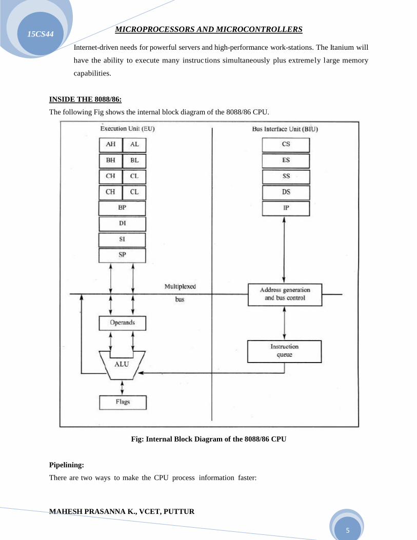
INSIDE THE 8088/86:
The following Fig shows the internal block diagram of the 8088/86 CPU.
Fig: Internal Block Diagram of the 8088/86 CPU
Pipelining:
There are two ways to make the CPU process information faster:

MICROPROCESSORS AND MICROCONTROLLERS
MAHESH PRASANNA K., VCET, PUTTUR
15CS44
6
1. Increase the working frequency – The designers can make the CPU work faster by increasing
the frequency under which it runs. But, it is technology dependent, meaning that the designer
must use whatever technology is available at the time, with consideration for cost. The
technology and materials used in making ICs (integrated circuits) determine the working
frequency, power consumption and the number of transistors packed into a single-chip
microprocessor.
2. Change the internal architecture of the CPU – The processing power of the CPU can be altered
by changing the internal working of the CPU. (In 8085, the CPU had to fetch an instruction
from memory, then execute it and then fetch again, execute it, and so on; i.e., 8085 CPU could
either fetch or execute at a given time).
The idea of pipelining is to allow the CPU to fetch and execute at the same time as shown in
following Fig.
Fig: Pipelined vs. Non-pipelined Execution
Intel implemented the concept of pipelining in the 8088/86 by splitting the internal structure of
the microprocessor into two sections:
o The execution unit (EU)
o The bus interface unit (BIU) – These two sections work simultaneously.
The BIU accesses memory and peripherals while the EU executes instructions
previously fetched.
This works only if the BIU keeps ahead of the EU; thus the BIU of the 8088/86 has
a buffer, or queue. The buffer is 4 bytes long in the 8088 and 6 bytes in the
8086. If any instruction takes too long to execute, the queue is filled to its
maximum capacity and the buses will sit idle.
The BIU fetches a new instruction whenever the queue has room for 2 bytes in
the 6-byte 8086 queue and for 1 byte in the 4-byte 8088 queue. In some
circumstances, the microprocessor must flush out the queue.

MICROPROCESSORS AND MICROCONTROLLERS
MAHESH PRASANNA K., VCET, PUTTUR
15CS44
7
For example, when a jump instruction is executed, the BIU starts to fetch
information from the new location in memory and information in the queue that
was fetched previously is discarded. In this situation the EU must wait until the
BIU fetches the new instruction. This is referred to in computer science
terminology as a branch penalty. In a pipelined CPU, this means that too
much jumping around reduces the efficiency of a program.
Pipelining in the 8088/86 has two stages, fetch and execute, but in more powerful
computers, pipelining can have many stages. The concept of pipelining
combined with an increased number of data bus pins has, in recent years, led to
the design of very powerful microprocessors.
Registers:
In the CPU, registers are used to store information temporarily. Information could ne one or two bytes of
data to be processed or the address of the data. The registers of 8088/86 fall into six categories; as given
in the following Table.
Table: Register of 8088/86/286 by Category
Category Bits Register Names
General 16 AX, BX, CX, DX
8 AH, AL, BH, BL, VH, CL, DH, DL
Pointer 16 SP (Stack Pointer), BP (Base Pointer)
Index 16 SI (Source Index), DI (Destination Index)
Segment 16 CS (Code Segment), DS (Data Segment), SS (Stack Segment), ES (Extra Segment)
Instruction 16 IP (Instruction Pointer)
Flag 16 FR (Flag Register)
The general-purpose registers in 8088/86 can be accessed as either 16-bit or 8-bit registers. All other
registers can be accessed only as the full 16 bits. In 8088/86, data types are either 8 or 16 bits. To access
12-bit data, a 16-bit register must be used with the highest 4 bits set to 0.
Fig: Structure of General-Purpose Register & Numbering Bits of a Register
Different registers in the 8088/86 are used for different functions . Some instructions use only specific
registers to perform their tasks. The first letter of each general-purpose register indicates its use:
AX is used for the accumulator
MICROPROCESSORS AND MICROCONTROLLERS
MAHESH PRASANNA K., VCET, PUTTUR
15CS44
8
BX as a base addressing register
CX as a counter in loop operations
DX to point to data in I/O operations.
INTRODUCTION TO ASSEMBLY PROGRAMMING:
o The CPU can work only in binary; it can do so at very high speeds. But, it is quite tedious
and slow for humans to deal with 0 s and 1 s in order to program the computer. A program
that consists of 0s and 1 s is called machine language.
o Although the hexadecimal system was used as a more efficient way to represent binary
numbers, the process of working in machine code was still cumbersome for humans.
Eventually, Assembly languages were developed, which provided mnemonics for the machine
code instructions, plus other ·features that made programming faster and less prone to error.
o The term mnemonic is typically used in computer science and engineering literature to refer to
codes and abbreviations that are relatively easy to remember.
o Assembly language programs ( A L P s ) must be translated into machine code by a program
called an assembler.
o Assembly language is referred to as a low-level language because it deals directly with the
internal structure of the CPU. To program in Assembly language, the programmer must know the
number of registers and their size, as well as other details of the CPU.
o Today, one can use many different programming languages, such as C/C++, BASIC, C#,
and numerous others. These languages are called high-level languages; because the
programmer does not have to be concerned with the internal details of the CPU.
o An assembler is used to translate an Assembly language program into machine code
(sometimes called object code); high-level languages are translated into machine code by a
program called a compiler. For instance, to write a program in C, one must use a C compiler to
translate the program into machine language.
o There are numerous assemblers available for translating x86 Assembly language programs into
machine code. M ost commonly used assemblers, MASM / TASM.
Assembly Language Programming:
An Assembly language program consists of –
A series of lines of Assembly language instructions –
An Assembly language instruction consists of a mnemonic
Optionally followed by one or two operands.

MICROPROCESSORS AND MICROCONTROLLERS
MAHESH PRASANNA K., VCET, PUTTUR
15CS44
9
The operands are the data items being manipulated, and the mnemonics are the commands to
the CPU, telling it what to do with those items.
E.g.:
Opcode (Mnemonic) Source operand (register
Relative addressing)
AGAIN: ADD AX, COUNT [BX] ; ADD ELEMENT OF COUNT TO AX.
Label—provides a Destination operand Comment
Means of branching (register addressing)
To this instruction
MOV Instruction:
The MOV instruction copies data from one location to another. The format is –
The Following Figure shows the operation of the MOV BX, CX instruction.
The MOV instruction does not affect the source operand. The following program first loads CL with
value 55H, then moves this value around to various registers inside the CPU.
The use of 16-bit registers is demonstrated below:

MICROPROCESSORS AND MICROCONTROLLERS
MAHESH PRASANNA K., VCET, PUTTUR
15CS44
10
In 8086 CPU, data can be moved among all the registers (except the flag register) as long as the source
and destination registers match in size.
Note the following three points with regarding MOV instruction:
1. Values cannot be loaded directly into any segment register (CS, DS, SS, and ES). To load a value
into a segment register, first load it to a non-segment register and then move it to the segment
register, as shown below.
2. If a value less than FFH is moved into a 16-bit register, the rest of the bits are assumed to be all
zeros. E.g.: MOV BX, 5 ; result will be BX = 0005, i.e., BH = 00 and BL = 05.
3. Moving a value that is too large into a register will cause an error.
ADD Instruction:
The ADD instruction has the following format –
The ADD instruction tells the CPU to add the source and the destination operands and put the result in the
destination.

MICROPROCESSORS AND MICROCONTROLLERS
MAHESH PRASANNA K., VCET, PUTTUR
15CS44
11
Executing above program results in AL (or DH) = 59H (25H + 34H = 59H) and BL (or CL) = 34H.
Notice that, the contents of the source operand do not change.
It is not necessary to move both data items into registers before adding them together.
Hence, for MOV and ADD instructions, the source operand may be an immediate data – this is called an
immediate operand. Please note, the destination operand has always been a register.
The largest number that an 8-bit register can hold is FFH. To use numbers larger than FFH (255 decimal),
16-bit registers (such as AX, BX, CX, or DX) must be used.
Running the above program(s) give DX (or CX) = 9F3H (34E + 6A5 = 9F3H) and AX = 34EH.
INTRODUCTION TO PROGRAM SEGMENTS:
A typical Assembly language program consists of at least three segments:
1. Code segment – contains the Assembly language instructions that perform the tasks that the
program was designed to accomplish.
2. Data segment – is used to store information (data) that needs to be processed by the instructions
in the code segment.
3. Stack segment – is used by the CPU to store i information temporarily.
Origin and Definition of the Segment:
A segment is an area of memory that includes up to 64K bytes and begins on an address evenly
divisible by 16 (such an address ends in 0H). In 8085, there was only 64K byte ( 21 6
= 1 6 K B ) of
memory for all code, data , and stack information; in the 8088/86 there can be up to 64K bytes of
memory assigned to each category. Within an Assembly language program, these categories are called
the code segment, data segment, and stack segment. For this reason, the 8088/86 can only handle a
maximum of 64K bytes of code, 64K bytes of data, and 64K bytes of stack at any .given time, all though it
has a range of 1 M b y t e s (220
= 1M bytes) of memory.
Logical Address and Physical Address:
There are three types of addresses mentioned with the 8086:
1. The physical address – is the 20-bit address that is actually put on the address pins of the 8086
microprocessor and decoded by memory interfacing circuitry. This is an actual physical location

MICROPROCESSORS AND MICROCONTROLLERS
MAHESH PRASANNA K., VCET, PUTTUR
15CS44
12
in RAM or ROM within the 1M byte memory range. This address can have a range of 00000H –
FFFFFH for the 8086, and real mode 286, 386, and 486 CPUs.
2. The offset address – is a location within a 64K byte segment range. Hence, an offset address can
range from 0000H – FFFFH.
3. The logical address – consists of a segment value and an offset address.
Fig: Illustration of Physical Address, Offset, and Logical Address
Code Segment:
To execute a program, the 8086 fetches the instruction (opcode and operands) from the code
segment. The logical address of an instruction always consists of a CS (code segment) and an IP
(instruction pointer), shown in the following Fig.
The physical address for the location of the instruction is generated by
o Shifting the CS left by one hex digit and then adding it to the IP. IP contains the offset address.
The resulting 20-bit address is called the physical address.
o To clarify this concept; assume values in CS and IP as shown in the above diagram. The offset
address is contained in IP; in this case it is 95F3H. The logical address is CS: IP, or 2500: 95F3H.
Then the physical address will be 25000 + 95F3 = 2E5F3H.
The physical address of an instruction can be calculated as follows:

MICROPROCESSORS AND MICROCONTROLLERS
MAHESH PRASANNA K., VCET, PUTTUR
15CS44
13
Fig: Calculation of Physical Address
The microprocessor will retrieve the instruction from memory locations starting at 2E5F3. Since IP can
have a minimum value of 0000H and a maximum of FFFFH; the logical address range in this example
is 2500:0000 to 2500: FFFF. This means that the lowest memory location of the code segment will be
25000H (25000+0000) and the highest memory location will be 34FFFH (25000+FFFF).
Logical Address vs. Physical Address in the Code Segment:
In the code segment, CS and IP hold the logical address of the instructions to be executed. The
following Assembly language instructions have been assembled (translated into machine code) and
stored in memory. The three columns show the logical address of CS: IP, the machine code stored at
that address, and the corresponding Assembly language code.
The program above shows that the byte at address 1132:0100 contains B0, which is the opcode for
moving a value into register AL, and address 1132:0I101I contains the operand (in this case 57) to be
moved to AL. Therefore, the instruction "MOV AL, 57” has a machine code of B057, where B0 is the
opcode and 57 is the operand.

MICROPROCESSORS AND MICROCONTROLLERS
MAHESH PRASANNA K., VCET, PUTTUR
15CS44
14
The following are the physical addresses and contents of each location for the above program.
Data Segment:
Assume that a program is being written to add 5 bytes of data, such as 25H, 12H, 15H, IFH, and 2BH.
One way to add them is as follows:
In the program above, the data and code are mixed together. The problem with wri ting the program
this way is that, if the data changes, the code must be searched for every place the data is included, and
the data retyped.
The idea to overcome the problem is to set aside an area of memory is strictly for data. In x86
microprocessors, the area of memory set aside for data is called the data segment. Just as the code
segment is associated with CS and IP as i ts segment register and offset, the data segment uses register
DS and an offset value .
The following demonstrates how data can be stored in the data segment and the program rewritten so
that it can be used for any set of data . Assume that the offset for the data segment begins at 200H.
NOTE:
1. The offset address is enclosed in brackets. The brackets indicate that the operand represents the
address of the data and not the data itself. If the brackets were not included, as in "MOV AL,
0200", the CPU would attempt to move 200 into AL instead of the contents of offset address
200.
2. DEBUG assumes that all numbers are in hex (no "H" suffix is required), whereas
MASM/ T A S M assumes that they are in decimal and the "H" must be included for hex data.

MICROPROCESSORS AND MICROCONTROLLERS
MAHESH PRASANNA K., VCET, PUTTUR
15CS44
15
This program will run with any set of data. Changing the data has no effect on the code. Although
this program is an improvement over the preceding one, it can be improved even further.
If the data had to be stored at a different offset address (say 450H), the program would have to
be rewritten. One way to solve this problem would be 'to use a register to hold the offset address, and
before each ADD, to increment the register to access the next byte.
The 8088/86 allows only the use of registers BX, SI, and DI as offset registers for the data
segment In other words, while CS uses only the IP register as an offset, DS uses only BX, DI, and SI
to hold the offset address of the data.
Table: Default Segments and Offset Register Pairs
Segment Offset Special Purpose
CS IP Instruction address
DS SI, DI, BX, an 8- or 16-bit number Data address
SS SP or BP Stack address
ES SI, DI, BX for string instructions String destination address
The term pointer is often used for a register holding an offset address. In the following example, BX is
used as a pointer.
The INC instruction adds 1 to (increments) its operand. "INC BX" achieves the same result as
"ADD BX, 1".
Logical Address and Physical Address in the Data Segment:
The physical address for data is calculated using the same rules as for the code segment. That is, the
physical address of data is calculated by shifting DS left one hex digit and adding the offset value, as
shown in following Examples.

MICROPROCESSORS AND MICROCONTROLLERS
MAHESH PRASANNA K., VCET, PUTTUR
15CS44
16
Little Endian Conversion:
Previous examples used 8-bit or 1-byte (16-bi ts) data. In this case the bytes are stored one after
another in memory. The 16-bit data can be used as follows:
In this case, the low byte goes to the low memory location and the high byte goes to the high memory
location. In the above example, memory location DS: 1500 contains F3H and memory location DS: 1501
contains 35H (DS: 1500 = F3 and DS: 1501 = 35). This is called little endian conversion.

MICROPROCESSORS AND MICROCONTROLLERS
MAHESH PRASANNA K., VCET, PUTTUR
15CS44
17
NOTE: In the big endian method, the high byte goes to the low address, where as in the little endian
method, the high byte goes to the high address and the low byte goes to the low address. All Intel
microprocessors use the little endian conversion.
Extra Segment (ES):
ES is a segment register used as an extra data segment. Its use is essential for string operations.
Memory map of IBM PC:
The 20-bit address of 8088/86 allows a total
of 1M bytes (1024K bytes) of memory
space with the address range 00000H –
FFFFFH. Memory map is the process of
allocating the 1M bytes of memory space to
various sections of the PC.
Out of 1MB –
640KB from the address 00000H –
9FFFFH were set aside for RAM;
the 128KB from A0000H – BFFFFH
were allocated for video memory;
the remaining 256KB from C0000H
– FFFFFH were set aside for ROM.
More about RAM:
In the early 1980s, most PCs came with only 64K to 256K bytes of RAM memory, which was
considered more than adequate at the time. Users had to buy memory expansion boards to expand
Fig: Memory Allocation in the PC

MICROPROCESSORS AND MICROCONTROLLERS
MAHESH PRASANNA K., VCET, PUTTUR
15CS44
18
memory up to 640K, if they needed additional memory. The need for expansion depends on the
Windows version being used and the memory needs of the application software being run.
The Windows operating system first allocates the available RAM on the PC for its own use
and then lets the rest be used for applications such as word processors. The complicated task of
managing RAM memory is left to Windows, since the amount of memory used by Windows varies
among its various versions and the memory needs of the application packages vary. For this reason we
do not assign any values f:or the CS, D S , and SS registers; since such an assignment means
specifying an exact physical address in the range 00000-9FFFFH , and this is beyond the knowledge
of the user.
Another reason is that assigning a physical address might work on a given PC but it might not
work on a PC with a different OS version and RAM size. In other w ords, the program would not be
portable to another PC.
Therefore, memory management is one of the most important functions of the operating system
and should be left to Windows.
Video RAM:
From A0000H to BFFFFH is set aside for video. The amount used and the location vary depending on the
video board installed on the PC.
More about ROM:
From C0000H to FFFFFH is set aside for ROM. Not all the memory space in this range is used by the
PC's ROM. Of this, 256K bytes, only the 64K bytes from location F0000H – FFFFFH are used by
BIOS (basic input/output system) ROM.
Some of the remaining space is used by various adapter cards (such as the network card), and
the rest is free. In recent years, newer versions of Windows have gained some very powerful
memory management capabilities and can put to good use all the unused memory space beyond 640.
The 640KB memory space from 00000 to 9FFFFH is referred to as conventional memory,
while the 384K bytes from A0000H to FFFFFH are called the UMB (upper memory block) in
Microsoft literature.
Functions of BIOS ROM:
Since the CPU can only execute programs that are stored in memory, there must be some permanent
(nonvolatile) memory to hold the programs, telling the CPU what to do when the power is turned on.
This collection of programs held by ROM is referred to as BIOS in the PC literature.

MICROPROCESSORS AND MICROCONTROLLERS
MAHESH PRASANNA K., VCET, PUTTUR
15CS44
19
BIOS, which stands for basic input-output system, contains programs to test RAM and other
components connected to the CPU. It also contains programs that allow Windows to communicate with
peripheral devices such as the keyboard, video, printer, and disk.
It is the function of BIOS to test all the devices connected to the PC when the computer is turned
on and to report any errors. For example, if the keyboard is disconnected from the PC before the
computer is turned on, BIOS will report an error on the screen, indicating that condition.
After testing and setting up the peripherals; BIOS will load Windows from disk into RAM and
hand over control of the PC to Windows. Windows always controls the PC once it is loaded.
THE STACK:
What is Stack, and Why is it Needed?
o There must be some place for the CPU to store information safely and temporary. The stack is a
section of read/write memory (RAM) used by the CPU to store information temporarily.
o The CPU needs this storage area since there are only a limited number of registers.
o The disadvantage of the stack is its access time – since the stack is in RAM, it takes much longer
to access compared to the access time of registers. Note that, the registers are inside the CPU and
RAM is outside.
How the Stack are Accessed?
o If the stack is a section of RAM, there must be registers inside the CPU to point to it.
o The two main registers used to access the stack are the SS (stack segment) register and the SP (stack
pointer) register.
o These registers must be loaded before any instructions accessing the stack are used.
o Every register inside the x86 (except segment registers and SP) can be stored in the stack and
brought back into the CPU from the stack memory.
o The storing of a CPU register in the stack is called a push, and loading the contents of the stack into
the CPU register is called a pop. In other words, a register is pushed onto the stack to store its
contents and popped off the stack to retrieve it.
o The job of the SP is very critical when push and pop are performed. In the x86, the stack pointer
register (SP) points at the current memory location used for the top of the stack and as data is
pushed onto the stack it is decremented. It is incremented as data is popped off the stack into the
CPU.
o When an instruction pushes or pops a general-purpose register, it must be the entire 16-bit regis ter.
In other words, one must code "PUSH AX "; there are no instructions such as "PUSH AL" or
"PUSH AH".

MICROPROCESSORS AND MICROCONTROLLERS
MAHESH PRASANNA K., VCET, PUTTUR
15CS44
20
o The reason that the SP is decremented after the push is to make sure that the stack is growing
downward from upper addresses to lower addresses. This is the opposite of the IP (instruction
pointer). As was seen in the preceding section, the IP points to the next instruction to be executed
and is incremented as each instruction is executed.
Pushing onto the Stack:
As each PUSH is executed, the contents of the registers are saved on the stack and SP is decremented by
2. For every byte of data saved on stack, SP is decremented.
Notice, how the data is stored on the stack. In the x86, the lower byte is always stored in the memory
location with the lower address.
Popping the Stack:
With every POP, the top 2 bytes of the stack are copied to the register specified by the instruction and the
stack pointer in incremented twice. Although the data actually remains in memory, it is not accessible
since the stack pointer is beyond that point.

MICROPROCESSORS AND MICROCONTROLLERS
MAHESH PRASANNA K., VCET, PUTTUR
15CS44
21
Logical Address vs. Physical Address for the Stack:
o The exact physical location of the stack depends on the value of the SS (stack segment) register
and SP (stack pointer). To compute the physical address for stack, shift left SS and then add
offset SP register.
o Memory management is the responsibility of the operating system. Hence, the Windows
operating system will assign the values for the SP and SS.
o The top of the stack is the last stack location occupied. BP is another register that can be used as
an offset into the stack.
Table: Default Segments and Offset Register Pairs
Segment Offset Special Purpose
CS IP Instruction address
DS SI, DI, BX, an 8- or 16-bit number Data address
SS SP or BP Stack address
ES SI, DI, BX for string instructions String destination address
NOTE:

MICROPROCESSORS AND MICROCONTROLLERS
MAHESH PRASANNA K., VCET, PUTTUR
15CS44
22
1. A single physical address may belong to many different logical addresses. This shows the
dynamic behavior of the segment and offset concept in the 8086 CPU.
2. When adding the offset to the shifted segment register; if an address beyond the maximum
allowed range (FFFFFH) is resulted, then wrap-around will occur.
3. In calculating the physical address, it is possible that two segments can overlap, as illustrated in
the following Fig.
Fig: Non-overlapping vs. Overlapping Segments
THE FLAG REGISTER:

MICROPROCESSORS AND MICROCONTROLLERS
MAHESH PRASANNA K., VCET, PUTTUR
15CS44
23
o The flag register is a 16-bit register sometimes referred to as the status register. Although the
register is 16 bits wide, only some of the bits are used. The rest are either undefined or reserved
by Intel.
o Six of the flags are called conditional flags, meaning that they indicate some condition that
resulted after an instruction was executed. These six are CF, PF, AF, ZF, SF, and OF.
o The three remaining flags are sometimes called control flags, since they are used to control the
operation of instructions before they are executed.
Fig: Flag Register
Key to remember: in One Day International Tendulkar Scored Zero, All People Cried.
Bits of the Flag Register:
CF, the Carry Flag – This flag is set whenever there is a carry out, either from d7 after an 8-bit
operation or from d 15 after a 16-bit data operation.
PF, the Parity Flag – After certain opera tions, the parity of the result's low-order byte is checked.
If the byte has an even number of 1 s, the parity flag is set to 1; otherwise, it is cleared.
AF, Auxiliary Carry Flag – If there is a carry from d3 to d4 of an operation, this bit is set; otherwise,
it is cleared (set equal to zero). This flag is used by the instructions that perform BCD (binary
coded decimal) arithmetic.
ZF, the Zero Flag – The zero flag is set to 1 if the result of arithmetic or logical operation is zero;
otherwise, it is cleared.
SF, the Sign Flag – Binary representation of signed numbers uses the most significant bit as the sign
bit. After arithmetic or logic operations, the status of this sign bit is copied into the SF, thereby
indicating the sign of the result.
TF, the Trap Flag – When this flag is set, it allows the program to single-step, meaning to ·execute one
instruction at a time. Single-stepping is used for debugging purposes.
0 1 2 3 4 5 6 7 8 9 10 11 12 13 14 15
0F DF IF TF SF ZF AF PF CF
BIT

MICROPROCESSORS AND MICROCONTROLLERS
MAHESH PRASANNA K., VCET, PUTTUR
15CS44
24
IF, Interrupt Enable Flag – This bit is set or cleared to enable or disable only the external
maskable interrupt requests.
DF, the Direction Flag – This bit is used to control the direction of string operations. If D = 1, the
registers are automatically decremented; if D = 0, the registers are automatically incremented. The state of
the D flag bit is controlled by STD (set D flag) and CLD (clear D flag) instructions.
OF, the Overflow Flag – This flag is set whenever the result of a signed number operation is too
large, causing the high-order bit to overflow into the sign bit. In general, the carry flag is used to
detect errors in unsigned arithmetic operations. The overflow flag is only used to detect errors in signed
arithmetic operations.
Flag Register and ADD Instruction:
The flag bits affected by the ADD instruction are CF, PF, AF, ZF, SF, and OF. The fo l lowing
examples a re given t o understand how each of these flag bits is affected. Please note that, MOV
instructions have no effect on the flag.

MICROPROCESSORS AND MICROCONTROLLERS
MAHESH PRASANNA K., VCET, PUTTUR
15CS44
25
Use of Zero Flag for Looping:
One of the most widely used applications of the flag register is the use of the zero flag to
implement program loops.
The t e r m loop refers to a set of instruct ions that is repeated a number of times. For
example, to add 5 bytes of data, a counter can be used to keep track of how many times the
loop needs to be repeated. Each time the addition is performed the counter is decremented
and the zero flag is checked. When the counter becomes zero, the zero flag is set (ZF =
1) and the loop is stopped.
MICROPROCESSORS AND MICROCONTROLLERS
MAHESH PRASANNA K., VCET, PUTTUR
15CS44
26
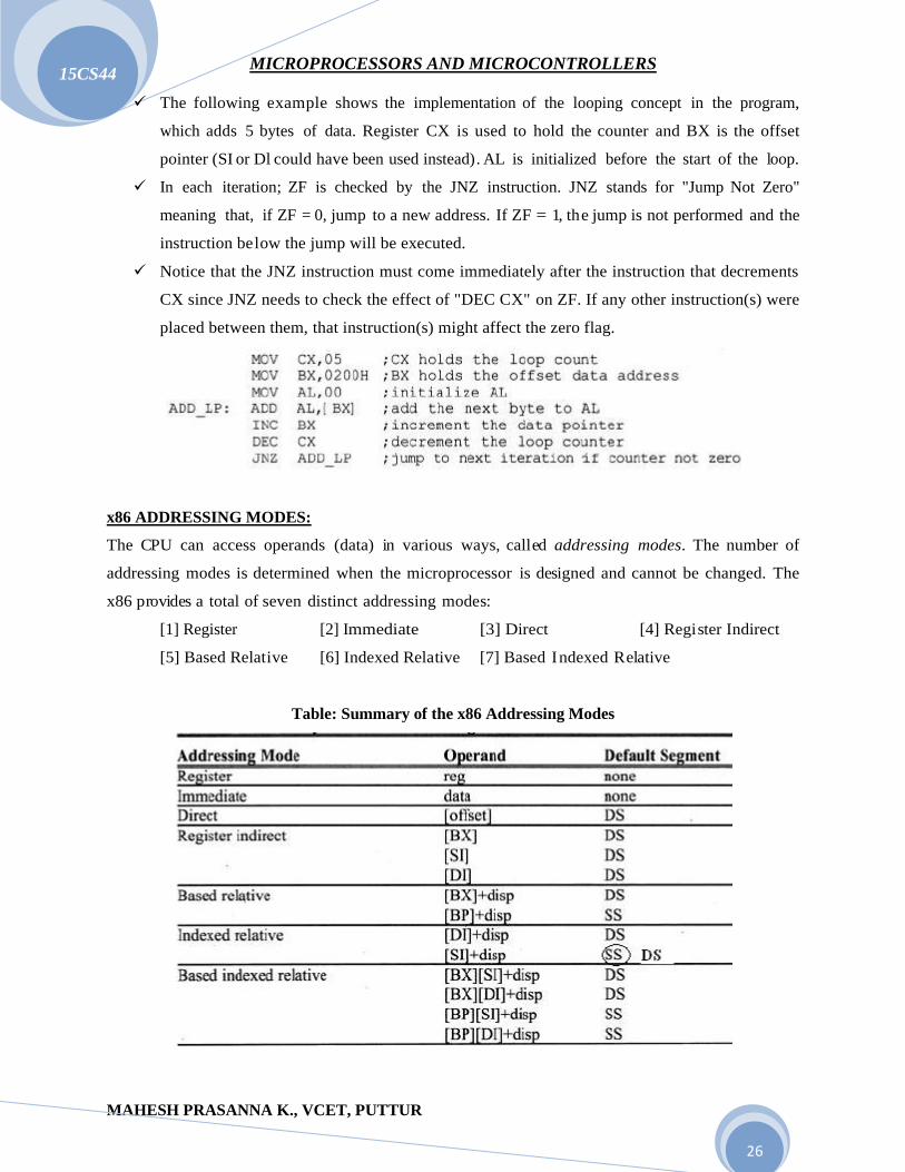
The following example shows the implementation of the looping concept in the program,
which adds 5 bytes of data. Register CX is used to hold the counter and BX is the offset
pointer (SI or Dl could have been used instead). AL is initialized before the start of the loop.
In each iteration; ZF is checked by the JNZ instruction. JNZ stands for "Jump Not Zero"
meaning that, if ZF = 0, jump to a new address. If ZF = 1, the jump is not performed and the
instruction below the jump will be executed.
Notice that the JNZ instruction must come immediately after the instruction that decrements
CX since JNZ needs to check the effect of "DEC CX" on ZF. If any other instruction(s) were
placed between them, that instruction(s) might affect the zero flag.
x86 ADDRESSING MODES:
The CPU can access operands (data) in various ways, called addressing modes. The number of
addressing modes is determined when the microprocessor is designed and cannot be changed. The
x86 provides a total of seven distinct addressing modes:
[1] Register [2] Immediate [3] Direct [4] Register Indirect
[5] Based Relative [6] Indexed Relative [7] Based Indexed Relative
Table: Summary of the x86 Addressing Modes

MICROPROCESSORS AND MICROCONTROLLERS
MAHESH PRASANNA K., VCET, PUTTUR
15CS44
27
1. Register Addressing Mode
The register addressing mode involves the use of registers to hold the data to be manipulated.
Memory is not accessed when this addressing mode is executed; therefore, it is relatively fast.
2. Immediate Addressing Mode
In immediate addressing mode (as the name implies), when the instruction is assembled, the operand
comes immediately after the opcode. For this reason, this addressing mode executes quickly. In this
addressing mode, the source operand is a constant. Immediate addressing mode can be used to load
information into any of the registers except the segment registers and flag registers.
3. Direct Addressing Mode
In the direct addressing mode, the data is in some memory location(s) and the address of the data in
memory comes immediately after the instruction. Note that, in immediate addressing mode, the operand
itself is provided with the instruction; whereas in direct addressing mode, the address of the operand is
provided with the instruction. This address is the offset address and one can calculate the physical address
by shifting left the DS register and adding it to the offset as follows:
PA = DS : Direct Address
Notice the bracket around the address. In the absence of this bracket, executing the command will give an
error since it is interpreted to move the value 2400 (16-bit data) into register DL, an 8-bit register.
Before After
MICROPROCESSORS AND MICROCONTROLLERS
MAHESH PRASANNA K., VCET, PUTTUR
15CS44
28
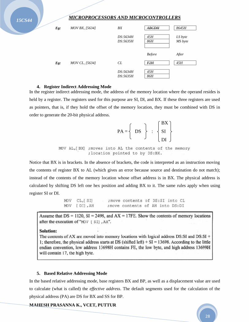
Eg: MOV BX, [5634] BX ABCDH 8645H
DS:5634H 45H LS byte
DS:5635H 86H MS byte
Before After
Eg: MOV CL, [5634] CL F2H 45H
DS:5634H 45H
DS:5635H 86H
4. Register Indirect Addressing Mode
In the register indirect addressing mode, the address of the memory location where the operand resides is
held by a register. The registers used for this purpose are SI, Dl, and BX. If these three registers are used
as pointers, that is, if they hold the offset of the memory location, they must be combined with DS in
order to generate the 20-bit physical address.
BX
PA = DS : SI
DI
Notice that BX is in brackets. In the absence of brackets, the code is interpreted as an instruction moving
the contents of register BX to AL (which gives an error because source and destination do not match);
instead of the contents of the memory location whose offset address is in BX. The physical address is
calculated by shifting DS left one hex position and adding BX to it. The same rules apply when using
register SI or DI.
5. Based Relative Addressing Mode
In the based relative addressing mode, base registers BX and BP, as well as a displacement value are used
to calculate (what is called) the effective address. The default segments used for the calculation of the
physical address (PA) are DS for BX and SS for BP.

MICROPROCESSORS AND MICROCONTROLLERS
MAHESH PRASANNA K., VCET, PUTTUR
15CS44
29
PA = DS BX
or : or + 8 or 16 bit displacement
SS BP
Alternative codings are “MOV CX, [BX+10]” or “MOV CX, 10[BX]”. In the case of BP register –
Alternative codings are “MOV AL, [BP+5]” or “MOV AL, 5[BP]”.
o In “MOV AL, [BP+5]”, BP+5 is called the effective address; since the 5th byte from the
beginning of the offset BP is moved to register AL. Similarly, in “MOV CX, [BX+10]”, BX+10
is called the effective address.
6. Indexed Relative Addressing Mode
The indexed relative addressing mode works the same as the based relative addressing mode, except that
registers DI and SI hold the offset address.
PA = DS SI
or : or + 8 or 16 bit displacement
SS DI
7. Based Indexed Addressing Mode
By combining based and indexed addressing modes, a new addressing mode is derived called the based
indexed addressing mode. In this mode, one base register and one index register are used.

MICROPROCESSORS AND MICROCONTROLLERS
MAHESH PRASANNA K., VCET, PUTTUR
15CS44
30
PA = DS BX SI
or : or + or + 8 or 16bit displacement
SS BP DI
The coding of the instructions above can vary. The last example can also be written as –
Segment Overrides:
The following Table summarizes the offset registers that can be used with the four segment registers.
Table: Default Segments and Offset Register Pairs
Segment Offset Special Purpose
CS IP Instruction address
DS SI, DI, BX, an 8- or 16-bit number Data address
SS SP or BP Stack address
ES SI, DI, BX for string instructions String destination address
The x86 CPU allows the program to override the default segment and use any segment register. To do
that, one needs to specify the segment in the code.
For example, in "MOV AL, [BX]", the physical address of the operand to be moved into AL is
DS: BX. To override that default, specify the desired segment in the instruction as "MOV AL, ES: [BX]
". Now the address of the operand being moved to AL is ES: BX instead of DS: BX.
The following Table shows more examples of segment overrides shown next to the default address in the
absence of the override.
Table: Sample Segment Overrides

MICROPROCESSORS AND MICROCONTROLLERS
MAHESH PRASANNA K., VCET, PUTTUR
15CS44
31
ASSEMBLY LANGUAGE PROGRAMMING
DIRECTIVES AND A SIMPLE PROGRAM:
A given Assembly language program (ALP) is a series of statements. There are two types of statements in
x86 ALP:
1. Assembly language instructions – instructions that are given to the microprocessor to do
the specific task. The Assembly language instruction can be translated into object code or
machine language. (E.g.: MOV, ADD, etc.)
2. Pseudo instructions/Directives – instructions that give directions to the assembler about
how it should translate the Assembly language instructions into machine code. These
instructions are not translated into machine code. They are used by the assembler to
organize the program as well as other output files. (E.g.: DB, DW, ASSUME, etc.)
An Assembly language instruction consists of four fields:
Brackets indicate that the field is optional; do not type the brackets.
E.g.:
Opcode (Mnemonic) Source operand (register
Relative addressing)
AGAIN: ADD AX, COUNT [BX] ; ADD ELEMENT OF COUNT TO AX.
Label—provides a Destination operand Comment
Means of branching (register addressing)
To this instruction
1. The label field allows the program to refer to a line of code by name. The label field cannot exceed 31
characters. Labels for directives do not need to end with a colon. A label must end with a colon when it
refers to an opcode generating instruction; the colon indicates to the assembler that this refers to code
within this code segment.
2, 3. The Assembly language mnemonic (instruction) and operand(s) fields together perform the real work
of the program and accomplish the tasks for which the program was written. In Assembly language
statements such as ADD AL, BL or MOV AX, 6764; ADD and MOV are mnemonic opcode, and “AL, BL”
and “AX, 6764” are the operands.
4. The comment filed begins with a “;”. The assembler ignores comments. The comments are optional,
but are highly recommended for someone to read and understand the program.

MICROPROCESSORS AND MICROCONTROLLERS
MAHESH PRASANNA K., VCET, PUTTUR
15CS44
32
Model Definition:
The first statement in an Assembly language program is the MODEL directive. This directive selects the
size of the memory model. Among the options for the memory model are SMALL, MEDIUM,
COMPACT, and LARGE.
•MODEL SMALL ; this directive defines the model as small
SMALL is one of the most widely used memory models for Assembly language programs This model
uses a maximum of 64K bytes of memory for code and another 64KB for data. The other models are
defined as follows:
Segment Definition:
The x86 CPU has four segment registers: CS (code segment), DS (data segment), SS (stack segment), and
ES (extra segment). Every line of an Assembly language program must correspond to one of these
segments. The simplified segment definition format uses three simple directives: ".CODE", ".DATA",
and ".STACK", which correspond to the CS, DS, and SS registers, respectively.
Segments of a Program:
Although one can write an Assembly language program that uses only one segment, normally a program
consists of at least three segments: the stack segment, the data segment, and the code segment.
Assembly language statements are grouped into segments in order to be recognized by the assembler and
consequently by the CPU.
The stack segment defines storage for the stack
The data segment defines the data that the program will use
The code segment contains the Assembly language instructions.

MICROPROCESSORS AND MICROCONTROLLERS
MAHESH PRASANNA K., VCET, PUTTUR
15CS44
33
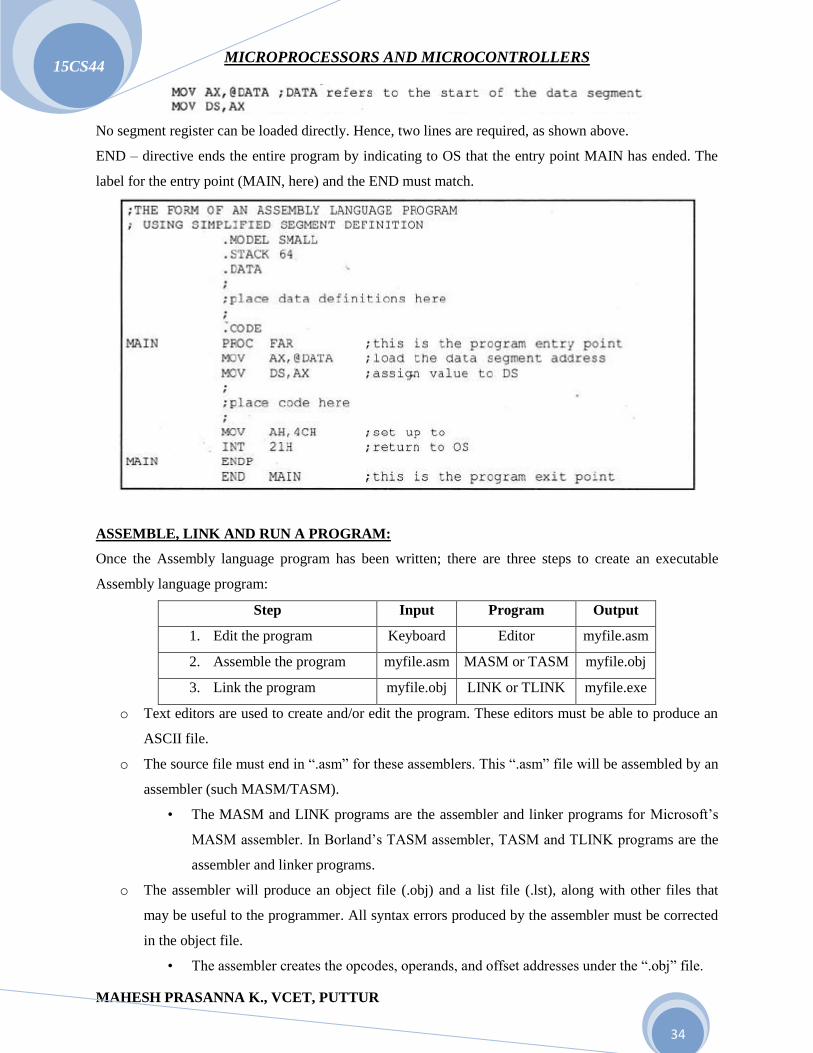
Fig: Simple Assembly Language Program
•MODEL SMALL – directive defines a model that uses a maximum of 64KB of memory for code and
another 64KB of memory for data.
•STACK 64 – directive reserves 64 bytes of memory for the stack.
•DATA – directive marks the beginning of the data segment.
The data segment defines three data items: DATA1, DATA2, and SUM. Each is defined as DB
(define byte). The DB directive is used by the assembler to allocate memory in byte-sized chunks.
Memory can be allocated in different sizes; such a 2 bytes, which has the directive DW (define
word).
The data items defined in the data segment can be accessed in the code segment by their labels.
DATA1 and DATA2 are given initial vales in the data section; and SUM in not given an initial
value, but storage is set aside for it.
•CODE – directive marks the beginning of the code segment.
MAIN – is the name (label) of procedure.
PROC – directive defines a procedure. A procedure is a group of instructions designed to
accomplish a specific function.
A PROC directive may have the option FAR or NEAR, which are the program entry point(s).
ENDP – directive defines the end of the procedure.
PROC and ENDP statements must have the same label (here it is MAIN).
It is the job of the OS (operating system) to assign exact values for the segment registers. When program
begins executing, the OS allocates some of RAM available to the segment registers. This is done as
follows:
MICROPROCESSORS AND MICROCONTROLLERS
MAHESH PRASANNA K., VCET, PUTTUR
15CS44
34
No segment register can be loaded directly. Hence, two lines are required, as shown above.
END – directive ends the entire program by indicating to OS that the entry point MAIN has ended. The
label for the entry point (MAIN, here) and the END must match.
ASSEMBLE, LINK AND RUN A PROGRAM:
Once the Assembly language program has been written; there are three steps to create an executable
Assembly language program:
Step Input Program Output
1. Edit the program Keyboard Editor myfile.asm
2. Assemble the program myfile.asm MASM or TASM myfile.obj
3. Link the program myfile.obj LINK or TLINK myfile.exe
o Text editors are used to create and/or edit the program. These editors must be able to produce an
ASCII file.
o The source file must end in “.asm” for these assemblers. This “.asm” file will be assembled by an
assembler (such MASM/TASM).
• The MASM and LINK programs are the assembler and linker programs for Microsoft’s
MASM assembler. In Borland’s TASM assembler, TASM and TLINK programs are the
assembler and linker programs.
o The assembler will produce an object file (.obj) and a list file (.lst), along with other files that
may be useful to the programmer. All syntax errors produced by the assembler must be corrected
in the object file.
• The assembler creates the opcodes, operands, and offset addresses under the “.obj” file.

MICROPROCESSORS AND MICROCONTROLLERS
MAHESH PRASANNA K., VCET, PUTTUR
15CS44
35
• The list file (.lst) lists all the opcodes and the offset addresses, as well as errors that the
assembler detected. This file can be displayed on the monitor by the command: C>type
myfile.lst | more.
• The cross-reference file (.crf) provides an alphabetical list of all symbols and tables used
in the program as well as program line numbers in which they are referenced.
o The object file (.obj) is the input for the LINK program, which produces the executable program
(.exe). The LINK program sets up the file, so that, it can be loaded by the OS and executed.
o We use DEBUG to execute the program and analyze the results.
• When the program is working successfully, it can be run at the OS level by typing the
command: C>myfile. When the program name is typed in at the OS level, the OS loads
the program in memory. This is referred as mapping; which means that the program is
mapped into the physical memory of the PC.
• When there are many segments for code or data, there is a need to see where each is
located and how many bytes are used by each. The “.map” file gives the name of each
segment, where it starts, where it stops, and its size in bytes.
Fig: Steps to Create a Program & Creating and Running the .exe File
PAGE and TITLE Directives:
The PAGE and the TITLE are two directives used make the “.lst” file more readable.

MICROPROCESSORS AND MICROCONTROLLERS
MAHESH PRASANNA K., VCET, PUTTUR
15CS44
36
The PAGE directive tells the printer how the list should be printed. In the default mode, the output will
have 66 lines per page and with a maximum of 80 characters per line. The default settings can be altered
to 60 and 132 as follows:
When the list is printed in more than one page, the assembler can be instructed to print the title of the
program on the top of each page by using the TITLE directive. The text after the TITLE pseudo-
instruction cannot be more than 60 ASCII characters.
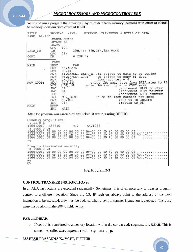
MORE SAMPLE PROGRAMS:
The following Fig shows the program and the list file generated when the program was assembled. After
the program was assembled and linked, DEBUG was used to dump the code segment to see what value is
assigned to the OS register. Remember that the value you get could be different for "MOV AX, xxxx" as
well as for CS in the program examples.

MICROPROCESSORS AND MICROCONTROLLERS
MAHESH PRASANNA K., VCET, PUTTUR
15CS44
37
Fig: Program 2-1
INC destination – adds 1 to the specified destination. The destination may be a register or
memory location.
Flags affected: AF, OF, PF, SF, and ZF. The CF is not affected.
Eg1: INC AL ; Add one to the contents of AL.
Eg2: INC BX ; Add one to the contents of BX.
DEC destination – subtract 1 from the specified destination. The destination may be a register or
a memory location.
Flags affected: AF, OF, PF, SF, and ZF. The CF is not affected.
Eg: DEC AL ; Subtract 1 from the contents of AL.
JNZ label – jump if not zero; if ZF = 0, jumps to the label specified. Checks for zero flag.

MICROPROCESSORS AND MICROCONTROLLERS
MAHESH PRASANNA K., VCET, PUTTUR
15CS44
38
Fig: MASM List for Program 2-1

MICROPROCESSORS AND MICROCONTROLLERS
MAHESH PRASANNA K., VCET, PUTTUR
15CS44
39
OFFSET: It is an operator which tells the assembler to determine the offset or displacement of a named
data item (variable) from the start of the segment.
Eg: MOV AX, OFFSET MES1 ; Loads the offset of variable MES1 in AX register.
Fig: Program 2-2
The ORG directive can be used to set the offset addresses for data items. In the above program, the ORG
directive causes SUM to be stored at DS: 0010.
MICROPROCESSORS AND MICROCONTROLLERS
MAHESH PRASANNA K., VCET, PUTTUR
15CS44
40
Fig: Program 2-3
CONTROL TRANSFER INSTRUCTIONS:
In an ALP, instructions are executed sequentially. Sometimes, it is often necessary to transfer program
control to a different location. Since the CS: IP registers always point to the address of the next
instruction to be executed; they must be updated when a control transfer instruction is executed. There are
many instructions in the x86 to achieve this.
FAR and NEAR:
o If control is transferred to a memory location within the current code segment, it is NEAR. This is
sometimes called intra-segment (within segment) jump.

MICROPROCESSORS AND MICROCONTROLLERS
MAHESH PRASANNA K., VCET, PUTTUR
15CS44
41
• In a NEAR jump, the IP is updated and CS remains the same, since control is still inside
the current code segment.
o If control is transferred to a memory location outside the current code segment, it is a FAR or
intersegment (between segments) jump.
• In a FAR jump, because control is passing outside the current code segment, both CS and
IP have to be updated to the new values.
Conditional Jumps:
In the conditional jump, control is transferred to a new location if a certain condition is met. The flag
register is the one that indicates the current condition. For example, with "JNZ label", the processor looks
at the zero flag to see if it is raised. If not, the CPU starts to fetch and execute instructions from the
address of the label. If ZF = I, it will not jump but will execute the next instruction below the JNZ.
Table: 8086 Conditional Jump Instructions
Short Jumps:
o All conditional jumps are short jumps. In a short jump, the address of the target must be within –
128 to +127 bytes of the IP.
o The conditional jump (short jump) is a two byte instruction: One byte is the opcode of the J
condition and the second byte is a value between 00 and FF.

MICROPROCESSORS AND MICROCONTROLLERS
MAHESH PRASANNA K., VCET, PUTTUR
15CS44
42
o An offset range of 00 to FF gives 256 possible addresses; these are split between backward jumps
(to –128) and forward jumps (to +127).
o In a jump backward, the second byte is the 2's complement of the displacement value. To
calculate the target address, the second byte is added to the IP of the instruction after the jump.
o The instruction "JNZ AGAIN" was assembled as "JNZ 000D", and 000D is the address of the
instruction with the label AGAIN. The instruction "JNZ 000D" has the opcode 75 and the target
address FA, which is located at offset addresses 0011 and 0012.
o This is followed by "MOV SUM, AL", which is located beginning at offset address 0013. The IP
value of this MOV (0013), is added to FA to calculate the address of label AGAIN (0013+ FA=
000D) and the carry is dropped.
o In reality, FA is the 2's complement of -6, meaning that the address of the target is -6 bytes from
the IP of the next instruction.
o Similarly, the target address for a forward jump is calculated by adding the IP of the following
instruction to the operand. In that case the displacement value is positive, as shown next.

MICROPROCESSORS AND MICROCONTROLLERS
MAHESH PRASANNA K., VCET, PUTTUR
15CS44
43
o In the program above, "JB NEXT" has the opcode 72 and the target address 06 and is located at
IP = 000A and 000B.
o The jump will be 6 bytes from the next instruction, which is IP = 000C. Adding gives us 000CH
+ 0006H = 0012H, which is the exact address of the NEXT label.
o Look also at "JA NEXT", which has 77 and 02 for the opcode and displacement, respectively.
The IP of the following instruction, 0010, is added to 02 to get 0012, the address of the target
location.
Note that, regardless of whether the jump is forward or backward, for conditional jumps, the address of
the target address can never be more than –128 to +127 bytes away from the IP associated with the
instruction following the jump lf any attempt is made to violate this rule, the assembler will generate a
"relative jump out of range" message. These conditional jumps are sometimes referred to as SHORT
jumps.
Unconditional Jumps:
"JMP label" is an unconditional jump in which control is transferred unconditionally to the target
location label. The unconditional jump can take the following forms:
1. SHORT JUMP – which is specified by the format "JMP SHORT label". This is a jump in which
the address of the target location is within –128 to +127 bytes of memory relative to the address
of the current IP.
In this case, the opcode is EB and the operand is 1 byte in the range 00 to FF. The
operand byte is added to the current IP to calculate the target address. If the jump is
backward, the operand is in 2's complement. This is exactly like the J condition case.
Coding the directive "short" makes the jump more efficient; i.e., it will be assembled into
a 2-byte instruction instead of a 3-byte instruction.
2. NEAR JUMP, which is the default, has the format "JNP label". This is a near jump (within the
current code segment) and has the opcode E9. The target address can be any of the addressing
modes of direct, register, register indirect, or memory indirect:
(a) Direct JUMP: is exactly like the short jump explained earlier, except that the target
address can be anywhere in the segment within the range +32767 to –32768 of the
current IP.
(b) Register indirect JUMP: the target address is in a register. For example, in "JMP
BX", IP takes the value BX.

MICROPROCESSORS AND MICROCONTROLLERS
MAHESH PRASANNA K., VCET, PUTTUR
15CS44
44
(c) Memory indirect JMP: the target address is the contents of two memory locations
pointed at by the register. Example: "JMP [DI]" will replace the IP with the contents of
memory locations pointed at by DI and DI + 1.
3. FAR JUMP, which has the format "JMP FAR PTR label". This is a jump out of the current code
segment, meaning that not only the IP but also the CS is replaced with new values.
CALL Statement:
o Another control transfer instruction is the CALL instruction, which is used to call a procedure.
CALLs to procedures are used to perform tasks that need to be performed frequently. This makes
a program more structured.
o The target address could be in the current segment, in which case it will be a NEAR call or
outside the current CS segment, which is a FAR call.
o To make sure that after execution of the called subroutine the microprocessor knows where to
come back, the microprocessor automatically saves the address of the instruction following the
call on the stack. It must be noted that in the NEAR call only the IP is saved on the stack, and in a
FAR call both CS and IP are saved.
o When a subroutine is called, control is transferred to that subroutine and the processor saves the
IP (and CS in the case of a FAR call) and begins to fetch instructions from the new location.
o After finishing execution of the subroutine, for control to be transferred back to the caller, the last
instruction in the called subroutine must be RET (return). The RET instruction in the case of
NEAR and FAR is different. For NEAR calls, the IP is restored; for FAR calls, both CS and IP
are restored.
o This will ensure that control is given back to the caller. As an example, assume that SP = FFFEH
and the following code is a portion of the program unassembled in DEBUG:

MICROPROCESSORS AND MICROCONTROLLERS
MAHESH PRASANNA K., VCET, PUTTUR
15CS44
45
Fig: IP in the Stack
Since the CALL instruction is a NEAR call, (different IP, same CS), only IP is saved on the stack. In this
case, the IP address of the instruction after the call is saved on the stack as shown in above Fig. This IP
will be 0206, which belongs to the "MOV AX, 142F" instruction.
The last instruction of the called subroutine must be a RET instruction that directs the CPU to
POP the top 2 bytes of the stack into the IP and resume executing at offset address 0206. For this reason,
the number of PUSH and POP instructions (which alter the SP) must match. In other words, for every
PUSH there must be a POP.
Assembly Language Subroutines:
In Assembly language programming it is common to have one main program and many subroutines to be
called from the main program. This allows you to make each subroutine into a separate module. Each
module can be tested separately and then brought together.
The main program is the entry point from the OS and is FAR, as explained earlier, but the
subroutines called within the main program can be FAR or NEAR. Remember that NEAR routines are in
the same code segment, while FAR routines are outside the current code segment. If there is no specific
mention of FAR after the directive PROC, by default, it will be NEAR, as shown in the following Fig.
Rules for Names in Assembly Language:
By choosing label names that are meaningful, a programmer can make a program much easier to
read and maintain. There are several rules that names must follow.
Each label name must be unique.
The names used for labels in Assembly language programming consist of alphabetic letters in
both upper- and lowercase, the digits 0 through 9, and the special characters question mark(?),
period(.), at(@), under line(_), and dollar sign ($).

MICROPROCESSORS AND MICROCONTROLLERS
MAHESH PRASANNA K., VCET, PUTTUR
15CS44
46
The first character of the name must be an alphabetic character or special character. It cannot be a
digit.
Names may be up to 31 characters long.
Fig: Shell of Assembly Language Subroutines
DATA TYPES AND DATA DEFINITIONS:
o The assembler supports all the various data types of the x86 microprocessor by providing data
directives that define the data types and set aside memory for them.
o The 8088/86 microprocessor supports many data types, but none are longer than 16 bits wide
since the size of the registers is 16 bits. It is the job of the programmer to break down data larger
than 16 bits (0000 to FFFFH, or 0 to 65535 in decimal) to be processed by the CPU.
o The data types used by the 8088/86 can be 8-bit or 16-bit, positive or negative. If a number is less
than 8 bits wide, it still must be coded as an 8-bit register with the higher digits as zero. Similarly,
if the number is less than 16 bits wide it must use all 16 bits, with the rest being 0s.
o For example, the number 5 is only 3 bits wide (101) in binary, but the 8088/86 will accept it as 05
or "0000 0101" in binary. The number 514 is "10 0000 0010" in binary, but the 8088/86 will
accept it as "0000 0010 0000 0010" in binary.
Assembler Data Directive:
MICROPROCESSORS AND MICROCONTROLLERS
MAHESH PRASANNA K., VCET, PUTTUR
15CS44
47
The following are some of the data directives used by the x86 microprocessor and supported by all
software vendors.
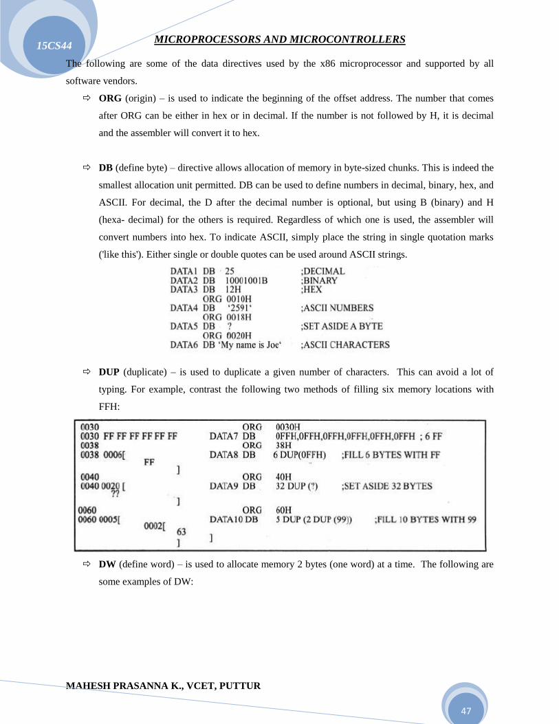
ORG (origin) – is used to indicate the beginning of the offset address. The number that comes
after ORG can be either in hex or in decimal. If the number is not followed by H, it is decimal
and the assembler will convert it to hex.
DB (define byte) – directive allows allocation of memory in byte-sized chunks. This is indeed the
smallest allocation unit permitted. DB can be used to define numbers in decimal, binary, hex, and
ASCII. For decimal, the D after the decimal number is optional, but using B (binary) and H
(hexa decimal) for the others is required. Regardless of which one is used, the assembler will
convert numbers into hex. To indicate ASCII, simply place the string in single quotation marks
('like this'). Either single or double quotes can be used around ASCII strings.
DUP (duplicate) – is used to duplicate a given number of characters. This can avoid a lot of
typing. For example, contrast the following two methods of filling six memory locations with
FFH:
DW (define word) – is used to allocate memory 2 bytes (one word) at a time. The following are
some examples of DW:

MICROPROCESSORS AND MICROCONTROLLERS
MAHESH PRASANNA K., VCET, PUTTUR
15CS44
48
EQU (equate) – is used to define a constant without occupying a memory location. EQU does not
set aside storage for a data item but associates a constant value with a data label so that when the
label appears in the program; its constant value will be substituted for the label.
o EQU can also be used outside the data segment, even in the middle of a code segment.
Using EQU for the counter constant in the immediate addressing mode:
COUNT EQU 25
When executing the instructions "MOV CX,
COUNT", the register CX will be loaded with the
value 25.
COUNT DB 25
When executing the same instruction "MOV CX,
COUNT" it will be in the direct addressing mode.
What is the real advantage of EQU? First, note that EQU can also be used in the data segment:
COUNT EQU 25
COUNTER1 DB COUNT
COUNTER2 DB COUNT
Assume that there is a constant (a fixed value) used in many different places in the data and code
segments. By the use of EQU, one can change it once and the assembler will change all of them, rather
than making the programmer tries to find every location and correct it.
DD (define double word) – directive is used to allocate memory locations that are 4 bytes (two
words) in size. Again, the data can be in decimal, binary, or hex. In any case the data is converted
to hex and placed in memory locations according to the rule of low byte to low address and high
byte to high address. DD examples are:
DQ (define quad word) – is used to allocate memory 8 bytes (four words) in size. This can be
used to represent any variable up to 64 bits wide:

MICROPROCESSORS AND MICROCONTROLLERS
MAHESH PRASANNA K., VCET, PUTTUR
15CS44
49
DT (define ten bytes) – is used for memory allocation of packed BCD numbers. The application
of DT will be seen in the multibyte addition of BCD numbers. For now, observe how they are
located in memory. Notice that the "H" after the data is not needed. This directive allocates 10
bytes, but a maximum of 18 digits can be entered.
It is essential to understand the way operands are stored in memory. The following Fig shows the memory
dump of the data section, including all the examples discussed here.
Looking at the memory dump shows that, all of the data directives use the little endian format for storing
data (the least significant byte is located in the memory location of the lower address and the most
significant byte resides in the memory location of the higher address).
For example, look at the case of "DATA20 DQ 4523C2", residing in memory starting at offset
00C0H. C2, the least significant byte, is in location 00C0, with 23 in 00C1, and 45, the most significant
byte, in 00C2. It must also be noted that for ASCII data, only the DB directive can be used to define data
of any length, and the use of DO, DQ, or DT directive for ASCII strings of more than 2 bytes gives an
assembly error. When DB is used for ASCII numbers, notice how it places them backwards in memory.
For example, see “DATA4 DB „2591‟ ” at origin 10H: 32, ASCII for 2, is in memory location 10H; 35,
ASCII for 5, is in 11H; and so on.

MICROPROCESSORS AND MICROCONTROLLERS
MAHESH PRASANNA K., VCET, PUTTUR
15CS44
50
FULL SEGMENT DEFINITION:
The way that segments have been defined in the programs above is a newer definition referred to as
simple segment definition. It is supported by Microsoft's MASM 5.0 and higher and/or Borland's TASM
version 1 and higher. The older, more traditional definition is called the full segment definition.
Segment Definition:
In the full segment definition, the ".MODEL" directive is not used. Further, the directives "
.STACK",".DATA", and" .CODE" are replaced by SEGMENT and ENDS directives that
surround each segment.
The SEGMENT and the ENDS directives indicate to the assembler the beginning and ending of a
segment and have the following format:
The label, or name, must follow naming conventions and must be unique.
The [options] field gives important information to the assembler for organizing the segment, but
is not required.
The ENDS label must be the same label as in the SEGMENT directive.
The following Fig shows the full segment definition and simplified format, side by side.

MICROPROCESSORS AND MICROCONTROLLERS
MAHESH PRASANNA K., VCET, PUTTUR
15CS44
51
Stack Segment Definition:
The stack segment shown below contains the line: "DB 64 DUP (?)" to reserve 64 bytes of memory for
the stack. The following three lines in full segment definition are comparable to ".STACK 64" in simple
definition:
Data Segment Definition:
In full segment definition, the SEGMENT directive names the data segment and must appear before the
data. The ENDS segment marks the end of the data segment:
Code Segment Definition:
The code segment also begins and ends with SEGMENT and ENDS directives:
Example:
Fig: Program 2-2, Rewritten with Full Segment Definition
In full segment definition, immediately after the PROC directive is the ASSUME directive, which
associates segment registers with specific segments by assuming that the segment register is equal
to the segment labels used in the program.

MICROPROCESSORS AND MICROCONTROLLERS
MAHESH PRASANNA K., VCET, PUTTUR
15CS44
52
If an extra segment had been used, ES would also be included in the ASSUME statement.
The ASSUME statement is needed because a given Assembly language program can have several
code segments; one or two or three or more data segments and more than one stack segment. But
only one of each can be addressed by the CPU at a given time; since, only one of each of the
segment registers available inside the CPU.
ASSUME tells the assembler which of the segments defined by the SEGMENT directives should
be used.
Using the emu8086 Assembler:
There is a simple and popular assembler called emu8086; that one can use for assembling the 8086
Assembly language programs. It is available from the www.emu8086.com website. Examine the
following Fig for screenshots using emu8086.
Fig: emu8086
NOTE: emu8086 requires putting brackets around variables, unlike MASM/TASM.

MICROPROCESSORS AND MICROCONTROLLERS
MAHESH PRASANNA K., VCET, PUTTUR
15CS44
53
EXE vs COM Files:
All program examples so far were designed to be assembled and linked into EXE files. The COM file,
similar to the EXE file, contains the executable machine code and can be run at the OS level.
Why COM Files?
The EXE file can be of any size. Due to limited amount of memory, one needs to have very
compact code in the form of COM file.
COM files are used because of their compactness, since they cannot be greater than 64K bytes.
The reason for the 64K-byte limit is that the COM file must fit into a single segment, and since in
the x86 the size of a segment is 64K bytes, the COM file cannot be larger than 64K.
To limit the size of the file to 64K bytes requires defining the data inside the code segment and
also using an area (the end area) of the code segment for the stack.
Table: EXE vs. COM File Format
EXE File COM File
1. Unlimited size 1. Maximum size 64K
bytes
2. Stack segment is defined 2. No stack segment
definition
3. Data segment is defined
3. Data segment is
defined in code
segment
4. Larger file (takes more memory) 4. Smaller file (takes
less memory)
5. Header block (contains information such as size, address location in
memory, and stack address of the EXE module), which occupies 512
bytes of memory precedes every EXE file
5. Does not have a
header file
FLOWCHARTS AND PSEUDOCODE:
Structured programming is a term used to denote programming techniques that can make a program easier
to code, debug, and maintain over time. There are certain principles that every structured program should
follow. Some of these are as follows:
1. The program should be designed before it is coded. By using techniques of flowcharting or
pseudocode, the design of the program is clear to the person coding it, as well as to those who
will maintain the program later.

MICROPROCESSORS AND MICROCONTROLLERS
MAHESH PRASANNA K., VCET, PUTTUR
15CS44
54
2. Using comments within the program and documentation accompanying the program also will
help someone else to know what the program does. It may even help the programmer who wrote
the program remember how it worked years later!
3. The main routine should consist of calls to subroutines that perform the work of the program.
This is sometimes called top-down programming. Use subroutines to accomplish tasks that are
repeated. This saves time in coding and also makes the program easier to read.
4. Data control is very important. It can be very frustrating and time consuming to track through a
long program to find where a variable was changed. First of all, the programmer should document
the purpose of each variable, and which subroutines might alter its value. Further, each subroutine
should document its input and output variables, and which input variables might be altered within
it.
Flow Charts & Pseudocode:
Flowcharts use graphic symbols to represent different types of program operations. These symbols are
connected together into a flowchart to show the flow of execution of the program.
Fig: Commonly used Flowchart Symbols
The limitations of flowchart are –
We can’t write much in the little boxes
We can’t get the clear picture of the program without getting bogged down in the details.
An alternative to using flowchart is pseudocode, which involves writing brief descriptions of the flow of
the code.
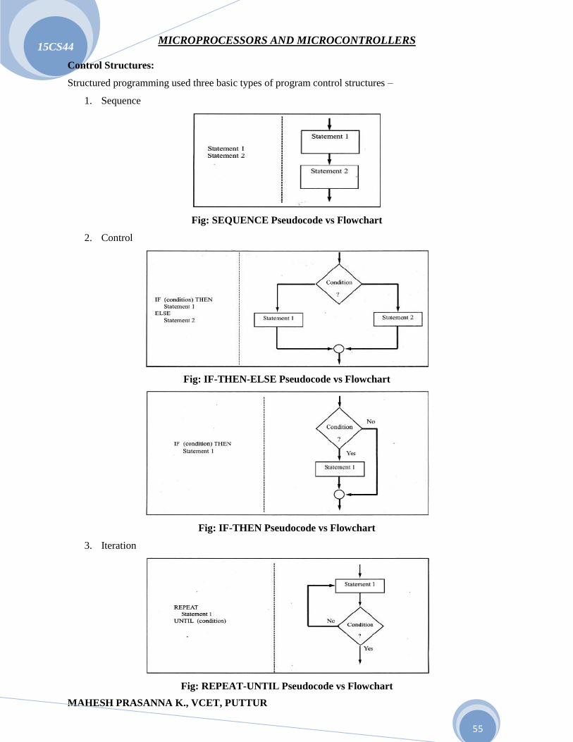
MICROPROCESSORS AND MICROCONTROLLERS
MAHESH PRASANNA K., VCET, PUTTUR
15CS44
55
Control Structures:
Structured programming used three basic types of program control structures –
1. Sequence
Fig: SEQUENCE Pseudocode vs Flowchart
2. Control
Fig: IF-THEN-ELSE Pseudocode vs Flowchart
Fig: IF-THEN Pseudocode vs Flowchart
3. Iteration
Fig: REPEAT-UNTIL Pseudocode vs Flowchart

MICROPROCESSORS AND MICROCONTROLLERS
MAHESH PRASANNA K., VCET, PUTTUR
15CS44
56
Fig: WHILE-DO Pseudocode vs Flowchart
The purpose of flowchart or pseudocode is to show the flow of the program and what the program does;
not the specific Assembly language instructions.
Fig: Flowchart vs Pseudocode for Program 2-1
By: Mahesh Prasanna K.,
Dept. of CSE, VCET.
____________*********____________
*********