microstrip filters for rf/microwave...
TRANSCRIPT

P1: OTA/XYZ P2: ABC
fm JWBS054-Hong November 17, 2010 8:49 Printer: Yet to come
Microstrip Filtersfor RF/MicrowaveApplicationsSecond Edition
JIA-SHENG HONG
A JOHN WILEY & SONS, INC., PUBLICATION
iii

P1: OTA/XYZ P2: ABC
fm JWBS054-Hong November 17, 2010 8:49 Printer: Yet to come
P1: OTA/XYZ P2: ABC
fm JWBS054-Hong November 17, 2010 8:49 Printer: Yet to come
Microstrip Filtersfor RF/MicrowaveApplications
i
P1: OTA/XYZ P2: ABC
fm JWBS054-Hong November 17, 2010 8:49 Printer: Yet to come
WILEY SERIES IN MICROWAVE AND OPTICAL ENGINEERING
KAI CHANG, EditorTexas A&M University
A complete list of the titles in this series appears at the end of this volume.
ii
P1: OTA/XYZ P2: ABC
fm JWBS054-Hong November 17, 2010 8:49 Printer: Yet to come
Microstrip Filtersfor RF/MicrowaveApplicationsSecond Edition
JIA-SHENG HONG
A JOHN WILEY & SONS, INC., PUBLICATION
iii
P1: OTA/XYZ P2: ABC
fm JWBS054-Hong November 17, 2010 8:49 Printer: Yet to come
Copyright C© 2011 by John Wiley & Sons, Inc. All rights reserved.
Published by John Wiley & Sons, Inc., Hoboken, New Jersey.Published simultaneously in Canada.
No part of this publication may be reproduced, stored in a retrieval system, or transmitted in any form orby any means, electronic, mechanical, photocopying, recording, scanning, or otherwise, except aspermitted under Section 107 or 108 of the 1976 United States Copyright Act, without either the priorwritten permission of the Publisher, or authorization through payment of the appropriate per-copy fee tothe Copyright Clearance Center, Inc., 222 Rosewood Drive, Danvers, MA 01923, (978) 750-8400,fax (978) 750-4470, or on the web at www.copyright.com. Requests to the Publisher for permissionshould be addressed to the Permissions Department, John Wiley & Sons, Inc., 111 River Street, Hoboken,NJ 07030, (201) 748-6011, fax (201) 748-6008, or online at http://www.wiley.com/go/permissions.
Limit of Liability/Disclaimer of Warranty: While the publisher and author have used their best efforts inpreparing this book, they make no representations or warranties with respect to the accuracy orcompleteness of the contents of this book and specifically disclaim any implied warranties ofmerchantability or fitness for a particular purpose. No warranty may be created or extended by salesrepresentatives or written sales materials. The advice and strategies contained herein may not be suitablefor your situation. You should consult with a professional where appropriate. Neither the publisher norauthor shall be liable for any loss of profit or any other commercial damages, including but not limited tospecial, incidental, consequential, or other damages.
For general information on our other products and services or for technical support, please contact ourCustomer Care Department within the United States at (800) 762-2974, outside the United States at(317) 572-3993 or fax (317) 572-4002.
Wiley also publishes its books in a variety of electronic formats. Some content that appears in print maynot be available in electronic formats. For more information about Wiley products, visit our web site atwww.wiley.com.
Library of Congress Cataloging-in-Publication Data:
Hong, Jia-Sheng.Microstrip filters for RF/microwave applications / Jia-Sheng Hong. – 2nd ed.
p. cm. – (Wiley series in microwave and optical engineering ; 216)Includes bibliographical references and index.
ISBN 978-0-470-40877-3 (hardback)1. Microwave circuits. 2. Strip transmission lines. 3. Electric filters. I. Title.
TK7876.H66 2011621.381′32–dc22 2010031085
Printed in Singapore
10 9 8 7 6 5 4 3 2 1
iv
P1: OTA/XYZ P2: ABC
fm JWBS054-Hong November 17, 2010 8:49 Printer: Yet to come
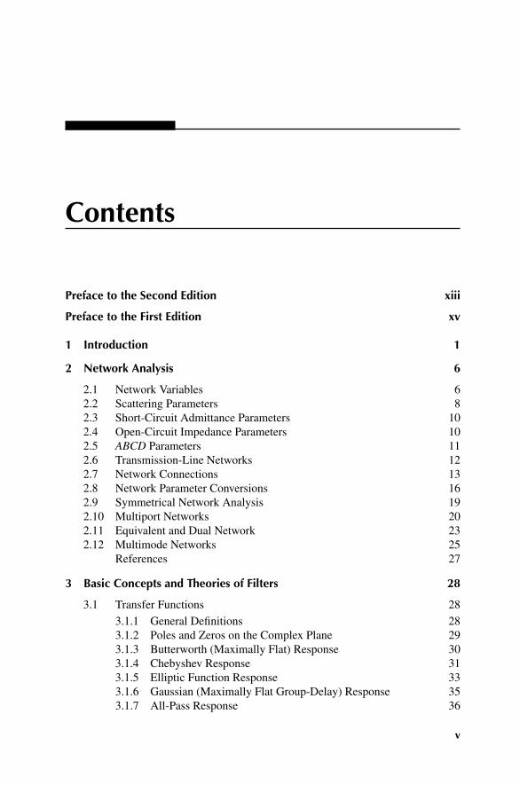
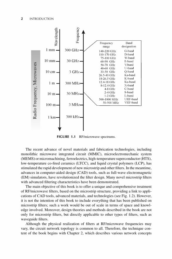
Contents
Preface to the Second Edition xiii
Preface to the First Edition xv
1 Introduction 1
2 Network Analysis 6
2.1 Network Variables 62.2 Scattering Parameters 82.3 Short-Circuit Admittance Parameters 102.4 Open-Circuit Impedance Parameters 102.5 ABCD Parameters 112.6 Transmission-Line Networks 122.7 Network Connections 132.8 Network Parameter Conversions 162.9 Symmetrical Network Analysis 192.10 Multiport Networks 202.11 Equivalent and Dual Network 232.12 Multimode Networks 25
References 27
3 Basic Concepts and Theories of Filters 28
3.1 Transfer Functions 28
3.1.1 General Definitions 283.1.2 Poles and Zeros on the Complex Plane 293.1.3 Butterworth (Maximally Flat) Response 303.1.4 Chebyshev Response 313.1.5 Elliptic Function Response 333.1.6 Gaussian (Maximally Flat Group-Delay) Response 353.1.7 All-Pass Response 36
v
P1: OTA/XYZ P2: ABC
fm JWBS054-Hong November 17, 2010 8:49 Printer: Yet to come
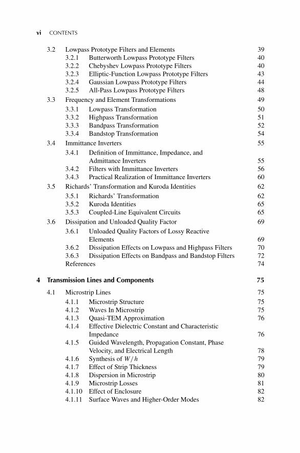
vi CONTENTS
3.2 Lowpass Prototype Filters and Elements 393.2.1 Butterworth Lowpass Prototype Filters 403.2.2 Chebyshev Lowpass Prototype Filters 403.2.3 Elliptic-Function Lowpass Prototype Filters 433.2.4 Gaussian Lowpass Prototype Filters 443.2.5 All-Pass Lowpass Prototype Filters 48
3.3 Frequency and Element Transformations 49
3.3.1 Lowpass Transformation 503.3.2 Highpass Transformation 513.3.3 Bandpass Transformation 523.3.4 Bandstop Transformation 54
3.4 Immittance Inverters 55
3.4.1 Definition of Immittance, Impedance, andAdmittance Inverters 55
3.4.2 Filters with Immittance Inverters 563.4.3 Practical Realization of Immittance Inverters 60
3.5 Richards’ Transformation and Kuroda Identities 62
3.5.1 Richards’ Transformation 623.5.2 Kuroda Identities 653.5.3 Coupled-Line Equivalent Circuits 65
3.6 Dissipation and Unloaded Quality Factor 69
3.6.1 Unloaded Quality Factors of Lossy ReactiveElements 69
3.6.2 Dissipation Effects on Lowpass and Highpass Filters 703.6.3 Dissipation Effects on Bandpass and Bandstop Filters 72References 74
4 Transmission Lines and Components 75
4.1 Microstrip Lines 75
4.1.1 Microstrip Structure 754.1.2 Waves In Microstrip 754.1.3 Quasi-TEM Approximation 764.1.4 Effective Dielectric Constant and Characteristic
Impedance 764.1.5 Guided Wavelength, Propagation Constant, Phase
Velocity, and Electrical Length 784.1.6 Synthesis of W/h 794.1.7 Effect of Strip Thickness 794.1.8 Dispersion in Microstrip 804.1.9 Microstrip Losses 814.1.10 Effect of Enclosure 824.1.11 Surface Waves and Higher-Order Modes 82
P1: OTA/XYZ P2: ABC
fm JWBS054-Hong November 17, 2010 8:49 Printer: Yet to come
CONTENTS vii
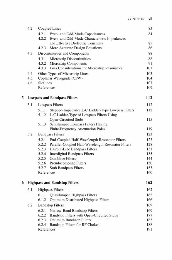
4.2 Coupled Lines 83
4.2.1 Even- and Odd-Mode Capacitances 844.2.2 Even- and Odd-Mode Characteristic Impedances
and Effective Dielectric Constants 854.2.3 More Accurate Design Equations 86
4.3 Discontinuities and Components 88
4.3.1 Microstrip Discontinuities 884.3.2 Microstrip Components 914.3.3 Loss Considerations for Microstrip Resonators 101
4.4 Other Types of Microstrip Lines 1034.5 Coplanar Waveguide (CPW) 1044.6 Slotlines 107
References 109
5 Lowpass and Bandpass Filters 112
5.1 Lowpass Filters 112
5.1.1 Stepped-Impedance L-C Ladder-Type Lowpass Filters 1125.1.2 L-C Ladder-Type of Lowpass Filters Using
Open-Circuited Stubs 1155.1.3 Semilumped Lowpass Filters Having
Finite-Frequency Attenuation Poles 119
5.2 Bandpass Filters 123
5.2.1 End-Coupled Half-Wavelength Resonator Filters 1235.2.2 Parallel-Coupled Half-Wavelength Resonator Filters 1285.2.3 Hairpin-Line Bandpass Filters 1315.2.4 Interdigital Bandpass Filters 1355.2.5 Combline Filters 1445.2.6 Pseudocombline Filters 1505.2.7 Stub Bandpass Filters 153References 160
6 Highpass and Bandstop Filters 162
6.1 Highpass Filters 162
6.1.1 Quasilumped Highpass Filters 1626.1.2 Optimum Distributed Highpass Filters 166
6.2 Bandstop Filters 169
6.2.1 Narrow-Band Bandstop Filters 1696.2.2 Bandstop Filters with Open-Circuited Stubs 1776.2.3 Optimum Bandstop Filters 1836.2.4 Bandstop Filters for RF Chokes 188References 191
P1: OTA/XYZ P2: ABC
fm JWBS054-Hong November 17, 2010 8:49 Printer: Yet to come
viii CONTENTS
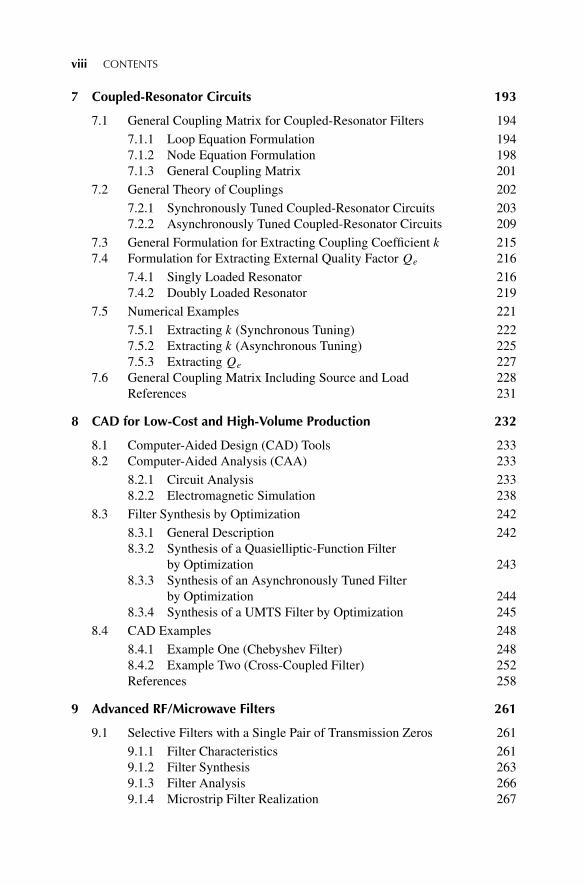
7 Coupled-Resonator Circuits 193
7.1 General Coupling Matrix for Coupled-Resonator Filters 194
7.1.1 Loop Equation Formulation 1947.1.2 Node Equation Formulation 1987.1.3 General Coupling Matrix 201
7.2 General Theory of Couplings 202
7.2.1 Synchronously Tuned Coupled-Resonator Circuits 2037.2.2 Asynchronously Tuned Coupled-Resonator Circuits 209
7.3 General Formulation for Extracting Coupling Coefficient k 2157.4 Formulation for Extracting External Quality Factor Qe 216
7.4.1 Singly Loaded Resonator 2167.4.2 Doubly Loaded Resonator 219
7.5 Numerical Examples 221
7.5.1 Extracting k (Synchronous Tuning) 2227.5.2 Extracting k (Asynchronous Tuning) 2257.5.3 Extracting Qe 227
7.6 General Coupling Matrix Including Source and Load 228References 231
8 CAD for Low-Cost and High-Volume Production 232
8.1 Computer-Aided Design (CAD) Tools 2338.2 Computer-Aided Analysis (CAA) 233
8.2.1 Circuit Analysis 2338.2.2 Electromagnetic Simulation 238
8.3 Filter Synthesis by Optimization 242
8.3.1 General Description 2428.3.2 Synthesis of a Quasielliptic-Function Filter
by Optimization 2438.3.3 Synthesis of an Asynchronously Tuned Filter
by Optimization 2448.3.4 Synthesis of a UMTS Filter by Optimization 245
8.4 CAD Examples 248
8.4.1 Example One (Chebyshev Filter) 2488.4.2 Example Two (Cross-Coupled Filter) 252References 258
9 Advanced RF/Microwave Filters 261
9.1 Selective Filters with a Single Pair of Transmission Zeros 261
9.1.1 Filter Characteristics 2619.1.2 Filter Synthesis 2639.1.3 Filter Analysis 2669.1.4 Microstrip Filter Realization 267
P1: OTA/XYZ P2: ABC
fm JWBS054-Hong November 17, 2010 8:49 Printer: Yet to come
CONTENTS ix
9.2 Cascaded Quadruplet (CQ) Filters 271
9.2.1 Microstrip CQ Filters 2719.2.2 Design Example 272
9.3 Trisection and Cascaded Trisection (CT) Filters 275
9.3.1 Characteristics of CT Filters 2759.3.2 Trisection Filters 2769.3.3 Microstrip Trisection Filters 2819.3.4 Microstrip CT Filters 284
9.4 Advanced Filters with Transmission-Line Inserted Inverters 287
9.4.1 Characteristics of Transmission-Line InsertedInverters 287
9.4.2 Filtering Characteristics with Transmission-LineInserted Inverters 289
9.4.3 General Transmission-Line Filter 294
9.5 Linear-Phase Filters 295
9.5.1 Prototype of Linear-Phase Filter 2969.5.2 Microstrip Linear-Phase Bandpass Filters 302
9.6 Extracted Pole Filters 304
9.6.1 Extracted Pole Synthesis Procedure 3069.6.2 Synthesis Example 3119.6.3 Microstrip-Extracted Pole Bandpass Filters 313
9.7 Canonical Filters 316
9.7.1 General Coupling Structure 3169.7.2 Elliptic-Function/Selective Linear-Phase
Canonical Filters 319
9.8 Multiband Filters 320
9.8.1 Filters Using Mixed Resonators 3219.8.2 Filters Using Dual-Band Resonators 3229.8.3 Filters Using Cross-Coupled Resonators 328References 332
10 Compact Filters and Filter Miniaturization 334
10.1 Miniature Open-Loop and Hairpin Resonator Filters 33410.2 Slow-Wave Resonator Filters 336
10.2.1 Capacitively Loaded Transmission-Line Resonator 33810.2.2 End-Coupled Slow-Wave Resonators Filters 34110.2.3 Slow-Wave, Open-Loop Resonator Filters 343
10.3 Miniature Dual-Mode Resonator Filters 349
10.3.1 Microstrip Dual-Mode Resonators 35010.3.2 Miniaturized Dual-Mode Resonator Filters 35210.3.3 Dual-Mode Triangular-Patch Resonator Filters 35510.3.4 Dual-Mode Open-Loop Filters 366
P1: OTA/XYZ P2: ABC
fm JWBS054-Hong November 17, 2010 8:49 Printer: Yet to come
x CONTENTS
10.4 Lumped-Element Filters 37910.5 Miniature Filters Using High Dielectric-Constant Substrates 38410.6 Multilayer Filters 386
10.6.1 Aperture-Coupled Resonator Filters 38610.6.2 Filters with Defected Ground Structures 39310.6.3 Substrate-Integrated Waveguide Filters 40410.6.4 LTCC and LCP Filters 412References 421
11 Superconducting Filters 433
11.1 High-Temperature Superconducting (HTS) Materials 433
11.1.1 Typical HTS Materials 43311.1.2 Complex Conductivity of Superconductors 43411.1.3 Penetration Depth of Superconductors 43511.1.4 Surface Impedance of Superconductors 43611.1.5 Nonlinearity of Superconductors 44011.1.6 Substrates for Superconductors 440
11.2 HTS Filters for Mobile Communications 441
11.2.1 HTS Filter with a Single Pair of Transmission Zeros 44211.2.2 HTS Filter with Two Pairs of Transmission Zeros 44811.2.3 HTS Filter with Group-Delay Equalization 454
11.3 HTS Filters for Satellite Communications 462
11.3.1 C-Band HTS Filter 46211.3.2 X-Band HTS Filter 46511.3.3 Ka-Band HTS Filter 468
11.4 HTS Filters for Radio Astronomy and Radar 469
11.4.1 Narrowband Miniature HTS Filter at UHF Band 47011.4.2 Wideband HTS Filter with Strong Coupling
Resonators 473
11.5 High-Power HTS Filters 47511.6 Cryogenic Package 479
References 480
12 Ultra-Wideband (UWB) Filters 488
12.1 UWB Filters with Short-Circuited Stubs 488
12.1.1 Design of Stub UWB Filters 48812.1.2 Stub UWB Filters with Improved Upper Stopband 490
12.2 UWB-Coupled Resonator Filters 495
12.2.1 Interdigital UWB Filters withMicrostrip/CPW-Coupled Resonators 495
12.2.2 Broadside-Coupled Slow-Wave ResonatorUWB Filters 501
P1: OTA/XYZ P2: ABC
fm JWBS054-Hong November 17, 2010 8:49 Printer: Yet to come
CONTENTS xi
12.2.3 UWB Filters Using Coupled Stepped-ImpedanceResonators 505
12.2.4 Multimode-Resonator UWB Filters 511
12.3 Quasilumped Element UWB Filters 520
12.3.1 Six-Pole Filter Design Example 52012.3.2 Eight-Pole Filter Design Example 526
12.4 UWB Filters Using Cascaded Miniature High- AndLowpass Filters 529
12.4.1 Miniature Wideband Highpass Filter 53012.4.2 Miniature Lowpass Filter 53312.4.3 Implementation of UWB Bandpass Filter 535
12.5 UWB Filters with Notch Band(s) 536
12.5.1 UWB Filters with Embedded Band Notch Stubs 53712.5.2 Notch Implementation Using Interdigital
Coupled Lines 54312.5.3 UWB Filters with Notched Bands Using
Vertically Coupled Resonators 550References 557
13 Tunable and Reconfigurable Filters 563
13.1 Tunable Combline Filters 56413.2 Tunable Open-Loop Filters without Via-Hole Grounding 57013.3 Reconfigurable Dual-Mode Bandpass Filters 574
13.3.1 Reconfigurable Dual-Mode Filter with Twodc Biases 574
13.3.2 Tunable Dual-Mode Filters Using a Singledc Bias 577
13.3.3 Tunable Four-Pole Dual-Mode Filter 588
13.4 Wideband Filters with Reconfigurable Bandwidth 59113.5 Reconfigurable UWB Filters 597
13.5.1 UWB Filter with Switchable Notch 59713.5.2 UWB Filter with Tunable Notch 60113.5.3 Miniature Reconfigurable UWB Filter 602
13.6 RF MEMS Reconfigurable Filters 604
13.6.1 MEMS and Micromachining 60413.6.2 Reconfigurable Filters Using RF MEMS Switches 608
13.7 Piezoelectric Transducer Tunable Filters 61013.8 Ferroelectric Tunable Filters 610
13.8.1 Ferroelectric Materials 61113.8.2 Ferroelectric Varactors 61213.8.3 Frequency Agile Filters Using Ferroelectrics 615References 619
P1: OTA/XYZ P2: ABC
fm JWBS054-Hong November 17, 2010 8:49 Printer: Yet to come
xii CONTENTS
Appendix: Useful Constants and Data 625
A.1 Physical Constants 625A.2 Conductivity of Metals at 25◦C (298K) 625A.3 Electical Resistivity ρ in 10−8 �m of Metals 626A.4 Properties of Dielectric Substrates 626
Index 627
P1: OTA/XYZ P2: ABC
fm JWBS054-Hong November 17, 2010 8:49 Printer: Yet to come
Preface to the Second Edition
The first edition of “Microstrip Filters for RF/Microwave Applications” was publishedin 2001. Over the years, this book has been well received and is used extensively inboth academy and industry by microwave researchers and engineers. From its incep-tion to publication, the book is almost 10 years old. While the fundamentals of filtercircuit have not changed, further innovations in filter realizations and other appli-cations have occurred, including changes in technology and use of new fabricationprocesses. There have been recent advances in RF MEMS and ferroelectric films fortunable filters; the use of liquid crystal polymer (LCP) substrates for multilayer cir-cuits, as well as the new filters for multiband and ultra-wideband (UWB) applications.
Although the microstrip remains as a main transmission line medium for thesenew developments, there has been a new trend of the combined use of other planartransmission line structures, such as co-planar waveguide (CPW), slotline and de-fected or slotted ground structures, for novel physical implementations beyond singlelayer in order to achieve filter miniaturization and better performance. Over the years,practitioners have also suggested topics that should be added for completeness, ordeleted in some cases, as they were not very useful in practice.
It is in response to these concerns that the 2nd edition of Microstrip Filters forRF/Microwave Applications has been written. The extensively revised book willoffer a thoroughly up-to-date professional reference focusing on microstrip and planarfilters, which find wide applications in today’s wireless, microwave, communications,and radar systems. It offers a unique comprehensive treatment of filters based on themicrostrip and planar structures and includes full design methodologies that areapplicable to waveguide and other transmission-line filters. The new edition includesa wealth of new materials including
� CPW and slotlines� General coupling matrix, including source and load� Multiband filters� Nondegenerate dual-mode filters
xiii
P1: OTA/XYZ P2: ABC
fm JWBS054-Hong November 17, 2010 8:49 Printer: Yet to come
xiv PREFACE TO THE SECOND EDITION
� Filters with defected ground structures� Substrate-integrated waveguide filters� Liquid crystal polymer (LCP) and LTCC multilayer filters� HTS filters for mobile/satellite communications and radio astronomy� Ultra-wideband (UWB) filters� Tunable and reconfigurable filters
Microstrip Filters for RF/Microwave Applications utilize numerous design ex-amples to demonstrate and emphasize computer-aided design with commerciallyavailable software. This intensively revised book, with cutting-edge information, re-mains not only a valuable design resource for partitions, but also a handy referencefor students and researchers in RF and microwave engineering.
I wish to acknowledge the financial supports of the UK EPSRC, Scottish En-terprise, BAE Systems (UK), and SELEX Galileo (UK). I would like to thanks allof my former and current research associates, PhD students, and visiting scholars,including Eamon McErlean, Dr. Young-Hoon Chun, Dr. Zhang-Cheng Hao, Dr. NeilThomson, Dr. Hussein Shaman, Dr. Sultan Alotaibi, Shuzhou Li, Wenxing Tang,and Alexander Miller, for their works, some of which are presented in the book.In addition, I would like to express my gratitude to several national and interna-tional collaborators, including Prof. Michael Lancaster and Dr. Tim Jackson (bothat University of Birmingham, UK), Dr. Paul Kirby (University of Cranfield, UK),Dr. Zheng Cui (Rutherford Appleton Laboratory, UK), Prof. Yusheng He (CAS,China), Alan Burdis and Colin Bird (both at SELEX Galileo, UK), and Dr. Keren Li(NiCT, Japan). The support provided by Dr. James Rautio and other members of staffat Sonnet Software Inc., USA, is acknowledged. I also wish to thank the colleagueswho I have worked with at Heriot-Watt University, including Prof. Marc Desmulliez,Prof. Alan Sangster, Dr. George Goussetis, Prof. Duncan Hand, Dr. Changhai Wang,and Dr. Paul Record.
Needless to say, I am indebted to many researchers for their published work,which have been rich sources of reference. My sincere gratitude extends to the Editorof Wiley series in microwave and optical engineering, Prof. Kai Chang; and theExecutive Editor of Wiley-Interscience, George Telecki, for their encouragement inwriting this new edition book. I am also indebted to my wife, Kai, and my son, Haide,without their support, writing this book would not have been possible.
Jia-Sheng Hong
2010
P1: OTA/XYZ P2: ABC
fm JWBS054-Hong November 17, 2010 8:49 Printer: Yet to come
Preface to the First Edition
Filters play important roles in many RF/microwave applications. Emerging appli-cations such as wireless communications continue to challenge RF/microwave fil-ters with ever more stringent requirements — higher performance, smaller size,lighter weight, and lower cost. The recent advance of novel materials and fabricationtechnologies, including high-temperature superconductors (HTS), low-temperaturecofired ceramics (LTCC), monolithic microwave-integrated circuit (MMIC), micro-electromechanic system (MEMS), and micro-machining technology, have stimulatedthe rapid development of new microstrip and other filters for RF/microwave ap-plications. In the meantime, advances in computer-aided design (CAD) tools, suchas full-wave electromagnetic (EM) simulators, have revolutionized the filter de-sign. Many novel microstrip filters with advanced filtering characteristics have beendemonstrated. However, up until now there has not been a single book dedicated tothis subject.
Microstrip Filters for RF/Microwave Applications offers a unique and comprehen-sive treatment of RF/microwave filters based on the microstrip structure, providinga link to applications of computer-aided design tools and advanced materials andtechnologies. Many novel and sophisticated filters using computer-aided design arediscussed, from basic concepts to practical realizations. The book is self-contained —it is not only a valuable design resource, but also a handy reference for students, re-searchers, and engineers in microwave engineering. It can also be used for RF/microwave education.
The outstanding features of this book include discussion of many novel microstripfilter configurations with advanced filtering characteristics, new design techniques,and methods for filter miniaturization. The book emphasizes computer analysis andsynthesis and full-wave electromagnetic (EM) simulation through a large number ofdesign examples. Applications of commercially available software are demonstrated.Commercial applications are included as are design theories and methodologies,which are not only for microstrip filters, but also directly applicable to other types offilters, such as waveguide and other transmission-line filters. Therefore, this book ismore than just a text on microstrip filters.
xv
P1: OTA/XYZ P2: ABC
fm JWBS054-Hong November 17, 2010 8:49 Printer: Yet to come
xvi PREFACE TO THE FIRST EDITION
Much of work described herein has resulted from the authors’ research. Theauthors wish to acknowledge the financial supports of the UK EPSRC and the Euro-pean Commission through the Advanced Communications Technologies and Services(ACTS) program. They would also like to acknowledge their national and interna-tional collaborators, including Professor Heinz Chaloupka at Wuppertal University(Germany), Robert Greed at Marconi Research Center (U.K.), Dr. Jean-Claude Mageat Thomson-CSF/CNRS (France), and Dieter Jedamzik formerly with GEC-MarconiMaterials Technology (U.K.).
The authors are indebted to many researchers for their published work, which wererich sources of reference. Their sincere gratitude extends to the Editor of Wiley seriesin microwave and optical engineering, Professor Kai Chang; the Executive Editor ofWiley-Interscience, George Telecki; and the reviewers for their support in writing thebook. The help provided by Cassie Craig and other members of the staff at Wiley ismost appreciated. The authors also wish to thank their colleagues at the Universityof Birmingham, including Professor Peter Hall, Dr. Fred Huang, Dr. Adrian Porch,and Dr. Peter Gardener.
In addition, Jia-Sheng Hong would like to thank Professor John Allen at theUniversity of Oxford (U.K.), Professor Werner Wiesbeck at Kalsruhe Universiy(Germany), and Dr. Nicholas Edwards at the British Telecom (U.K.) for their manyyears’ support and friendship. Professor Joseph Helszajn at Heriot-Watt University(U.K.), who sent his own book on filters to Jia-Sheng Hong, is also acknowledged.
Finally, Jia-Sheng Hong would like to express his deep appreciation to his wife,Kai, and his son, Haide, for their tolerance and support, which allowed him to writethe book at home over many evenings, weekends, and holidays. In particular, withoutthe help of Kai, completing this book on time would not have been possible.
Jia-Sheng HongM. J. Lancaster
2001
P1: OTA/XYZ P2: ABC
c01 JWBS054-Hong November 16, 2010 6:45 Printer: Yet to come
CHAPTER ONE
Introduction
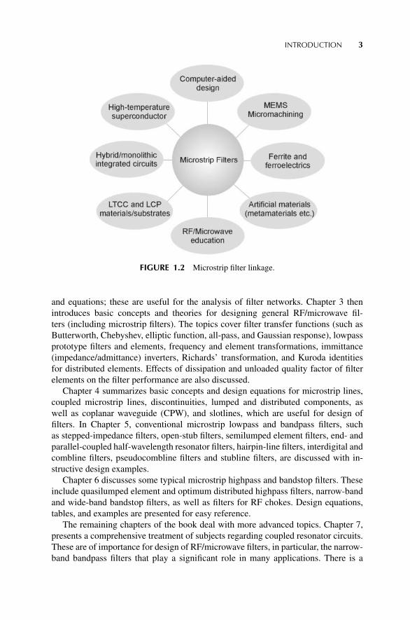
The term microwaves may be used to describe electromagnetic (EM) waves withfrequencies ranging from 300 MHz to 300 GHz, which correspond to wavelengths(in free space) from 1 m to 1 mm. The EM waves with frequencies above 30 and upto 300 GHz are also called millimeter waves, because their wavelengths are in themillimeter range (1−10 mm). Above the millimeter wave spectrum is the infrared,which comprises electromagnetic waves with wavelengths between 1 µm (10−6 m)and 1 mm. Beyond the infrared spectrum is the visible optical spectrum, the ultravioletspectrum, and x rays. Below the microwave frequency spectrum is the radio-frequency(RF) spectrum. The frequency boundary between RF and microwaves is somewhatarbitrary, depending on the particular technologies developed for the exploitation ofthat specific frequency range. Therefore, by extension, the RF/microwave applicationscan be referred to as communications, radar, navigation, radio astronomy, sensing,medical instrumentation, and others that explore the usage of frequency spectrumsin the range, for example, 300 kHz up to 300 GHz (Fig. 1.1). For convenience,some of these frequency spectrums are further divided into many frequency bands,as indicated in Fig. 1.1.
Filters play important roles in many RF/microwave applications. They are usedto separate or combine different frequencies. The electromagnetic spectrum is lim-ited and has to be shared; filters are used to select or confine the RF/microwavesignals within assigned spectral limits. Emerging applications, such as wireless com-munications, continue to challenge RF/microwave filters with ever more stringentrequirements — higher performance, more functionalities such as tunable or recon-figurable, smaller size, lighter weight, and lower cost. Depending on the requirementsand specifications, RF/microwave filters may be designed as lumped element or dis-tributed element circuits, they may be realized in various transmission-line structures,such as waveguide, coaxial line, coplanar waveguide (CPW), slotline, and microstrip.
Microstrip Filters for RF/Microwave Applications by Jia-Sheng HongCopyright C© 2011 John Wiley & Sons, Inc.
1
P1: OTA/XYZ P2: ABC
c01 JWBS054-Hong November 16, 2010 6:45 Printer: Yet to come
2 INTRODUCTION
FIGURE 1.1 RF/microwave spectrums.
The recent advance of novel materials and fabrication technologies, includingmonolithic microwave integrated circuit (MMIC), microelectromechanic system(MEMS) or micromachining, ferroelectrics, high-temperature superconductor (HTS),low-temperature co-fired ceramics (LTCC), and liquid crystal polymers (LCP), hasstimulated the rapid development of new microstrip and other filters. In the meantime,advances in computer-aided design (CAD) tools, such as full-wave electromagnetic(EM) simulators, have revolutionized the filter design. Many novel microstrip filterswith advanced filtering characteristics have been demonstrated.
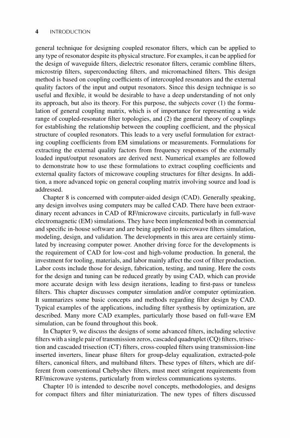
The main objective of this book is to offer a unique and comprehensive treatmentof RF/microwave filters, based on the microstrip structure, providing a link to appli-cations of CAD tools, advanced materials, and technologies (see Fig. 1.2). However,it is not the intention of this book to include everything that has been published onmicrostrip filters; such a work would be out of scale in terms of space and knowl-edge involved. Moreover, design theories and methods described in the book are notonly for microstrip filters, but directly applicable to other types of filters, such aswaveguide filters.
Although the physical realization of filters at RF/microwave frequencies mayvary, the circuit network topology is common to all. Therefore, the technique con-tent of the book begins with Chapter 2, which describes various network concepts
P1: OTA/XYZ P2: ABC
c01 JWBS054-Hong November 16, 2010 6:45 Printer: Yet to come
INTRODUCTION 3
FIGURE 1.2 Microstrip filter linkage.
and equations; these are useful for the analysis of filter networks. Chapter 3 thenintroduces basic concepts and theories for designing general RF/microwave fil-ters (including microstrip filters). The topics cover filter transfer functions (such asButterworth, Chebyshev, elliptic function, all-pass, and Gaussian response), lowpassprototype filters and elements, frequency and element transformations, immittance(impedance/admittance) inverters, Richards’ transformation, and Kuroda identitiesfor distributed elements. Effects of dissipation and unloaded quality factor of filterelements on the filter performance are also discussed.
Chapter 4 summarizes basic concepts and design equations for microstrip lines,coupled microstrip lines, discontinuities, lumped and distributed components, aswell as coplanar waveguide (CPW), and slotlines, which are useful for design offilters. In Chapter 5, conventional microstrip lowpass and bandpass filters, suchas stepped-impedance filters, open-stub filters, semilumped element filters, end- andparallel-coupled half-wavelength resonator filters, hairpin-line filters, interdigital andcombline filters, pseudocombline filters and stubline filters, are discussed with in-structive design examples.
Chapter 6 discusses some typical microstrip highpass and bandstop filters. Theseinclude quasilumped element and optimum distributed highpass filters, narrow-bandand wide-band bandstop filters, as well as filters for RF chokes. Design equations,tables, and examples are presented for easy reference.
The remaining chapters of the book deal with more advanced topics. Chapter 7,presents a comprehensive treatment of subjects regarding coupled resonator circuits.These are of importance for design of RF/microwave filters, in particular, the narrow-band bandpass filters that play a significant role in many applications. There is a
P1: OTA/XYZ P2: ABC
c01 JWBS054-Hong November 16, 2010 6:45 Printer: Yet to come
4 INTRODUCTION
general technique for designing coupled resonator filters, which can be applied toany type of resonator despite its physical structure. For examples, it can be applied forthe design of waveguide filters, dielectric resonator filters, ceramic combline filters,microstrip filters, superconducting filters, and micromachined filters. This designmethod is based on coupling coefficients of intercoupled resonators and the externalquality factors of the input and output resonators. Since this design technique is souseful and flexible, it would be desirable to have a deep understanding of not onlyits approach, but also its theory. For this purpose, the subjects cover (1) the formu-lation of general coupling matrix, which is of importance for representing a widerange of coupled-resonator filter topologies, and (2) the general theory of couplingsfor establishing the relationship between the coupling coefficient, and the physicalstructure of coupled resonators. This leads to a very useful formulation for extract-ing coupling coefficients from EM simulations or measurements. Formulations forextracting the external quality factors from frequency responses of the externallyloaded input/output resonators are derived next. Numerical examples are followedto demonstrate how to use these formulations to extract coupling coefficients andexternal quality factors of microwave coupling structures for filter designs. In addi-tion, a more advanced topic on general coupling matrix involving source and load isaddressed.
Chapter 8 is concerned with computer-aided design (CAD). Generally speaking,any design involves using computers may be called CAD. There have been extraor-dinary recent advances in CAD of RF/microwave circuits, particularly in full-waveelectromagnetic (EM) simulations. They have been implemented both in commercialand specific in-house software and are being applied to microwave filters simulation,modeling, design, and validation. The developments in this area are certainly stimu-lated by increasing computer power. Another driving force for the developments isthe requirement of CAD for low-cost and high-volume production. In general, theinvestment for tooling, materials, and labor mainly affect the cost of filter production.Labor costs include those for design, fabrication, testing, and tuning. Here the costsfor the design and tuning can be reduced greatly by using CAD, which can providemore accurate design with less design iterations, leading to first-pass or tunelessfilters. This chapter discusses computer simulation and/or computer optimization.It summarizes some basic concepts and methods regarding filter design by CAD.Typical examples of the applications, including filter synthesis by optimization, aredescribed. Many more CAD examples, particularly those based on full-wave EMsimulation, can be found throughout this book.
In Chapter 9, we discuss the designs of some advanced filters, including selectivefilters with a single pair of transmission zeros, cascaded quadruplet (CQ) filters, trisec-tion and cascaded trisection (CT) filters, cross-coupled filters using transmission-lineinserted inverters, linear phase filters for group-delay equalization, extracted-polefilters, canonical filters, and multiband filters. These types of filters, which are dif-ferent from conventional Chebyshev filters, must meet stringent requirements fromRF/microwave systems, particularly from wireless communications systems.
Chapter 10 is intended to describe novel concepts, methodologies, and designsfor compact filters and filter miniaturization. The new types of filters discussed
P1: OTA/XYZ P2: ABC
c01 JWBS054-Hong November 16, 2010 6:45 Printer: Yet to come
INTRODUCTION 5
include compact open-loop and hairpin resonator filters, slow-wave resonator filters,miniaturized dual-mode filters using degenerate or nondegenerate modes, lumped-element filters, filters using high dielectric constant substrates, and multilayer filters.The last topic covers aperture-coupled resonator filters, filters with defected or slotted-ground structures, substrate integrated waveguide filters, as well as low-temperaturecofired ceramics (LTCC) and liquid crystal polymer (LCP) filters.
Chapter 11 introduces high-temperature superconductors (HTS) for RF/microwave filter applications. It covers some important properties of superconduc-tors and substrates for growing HTS films, which are essential for the design of HTSmicrostrip filters. Typical superconducting filters with super performance for mobileand satellite communications, as well as radio astronomy and radar applications, aredescribed in this chapter.
Chapter 12 focuses on ultra-wideband (UWB) filters, which are a key compo-nent for many promising modern applications of UWB technology. In this chapter,typical types of UWB filters are described. This includes UWB filters comprised ofshort-circuit stubs, UWB filters using coupled single-mode or multimode resonators,quasilumped element UWB filters, UWB filters based on cascaded highpass andlowpass filters, and UWB filters with single- or multiple-notched bands.
The final chapter of the book (Chapter 13) is concerned with electronically tun-able and reconfigurable filters. In general, to develop an electronically reconfigurablefilter, active switching or tuning elements, such as semiconductor p-i-n and var-actor diodes, RF MEMS or other functional material-based components, includingferroelectric varactors and piezoelectric transducers need to be integrated within apassive filtering structure. Typical filters of these types are described in this chapter,which include tunable combline filters, tunable open-loop filters without using anyvia-hole connections, reconfigurable dual-mode filters, wideband filters with recon-figurable bandwidth, reconfigurable UWB filters, RF MEMS reconfigurable filters,piezoelectric transducer tunable filters, and ferroelectric tunable filters.
P1: OTA/XYZ P2: ABC
c02 JWBS054-Hong November 16, 2010 6:46 Printer: Yet to come
CHAPTER TWO
Network Analysis
Filter networks are essential building elements in many areas of RF/microwaveengineering. Such networks are used to select/reject or separate/combine signals atdifferent frequencies in a host of RF/microwave systems and equipments. Althoughthe physical realization of filters at RF/microwave frequencies may vary, the circuitnetwork topology is common to all.
At microwave frequencies, the use of voltmeters and ammeters for the directmeasurement of voltages and currents do not exist. For this reason, voltage andcurrent, as a measure of the level of electrical excitation of a network, do not play aprimary role at microwave frequencies. On the other hand, it is useful to be able todescribe the operation of a microwave network, such as a filter, in terms of voltages,currents, and impedances in order to make optimum use of low-frequency networkconcepts.
It is the purpose of this chapter to describe various network concepts and provideequations [1–10] that are useful for the analysis of filter networks.
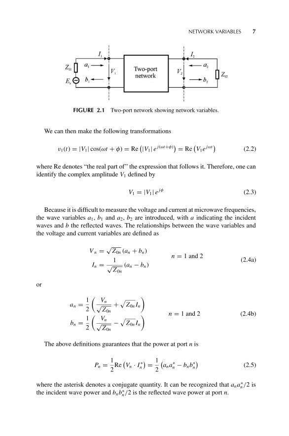
2.1 NETWORK VARIABLES
Most RF/microwave filters and filter components can be represented by a two-portnetwork, as shown in Figure 2.1, where V1, V2 and I1, I2 are the voltage and currentvariables at ports 1 and 2, respectively, Z01 and Z02 are the terminal impedances,and Es is the source or generator voltage. Note that the voltage and current variablesare complex amplitudes when we consider sinusoidal quantities. For example, asinusoidal voltage at port 1 is given by
v1(t) = |V1| cos(ωt + φ) (2.1)
Microstrip Filters for RF/Microwave Applications by Jia-Sheng HongCopyright C© 2011 John Wiley & Sons, Inc.
6
P1: OTA/XYZ P2: ABC
c02 JWBS054-Hong November 16, 2010 6:46 Printer: Yet to come
NETWORK VARIABLES 7
FIGURE 2.1 Two-port network showing network variables.
We can then make the following transformations
v1(t) = |V1| cos(ωt + φ) = Re(|V1| ej (ωt+φ)
) = Re(V1e
jωt)
(2.2)
where Re denotes “the real part of” the expression that follows it. Therefore, one canidentify the complex amplitude V1 defined by
V1 = |V1| ejφ (2.3)
Because it is difficult to measure the voltage and current at microwave frequencies,the wave variables a1, b1 and a2, b2 are introduced, with a indicating the incidentwaves and b the reflected waves. The relationships between the wave variables andthe voltage and current variables are defined as
V n = √Z0n (an + bn)
n = 1 and 2In = 1√
Z0n
(an − bn)(2.4a)
or
an = 1
2
(Vn√Z0n
+√
Z0nIn
)
n = 1 and 2
bn = 1
2
(Vn√Z0n
−√
Z0nIn
) (2.4b)
The above definitions guarantees that the power at port n is
Pn = 1
2Re
(Vn · I ∗
n
) = 1
2
(ana
∗n − bnb
∗n
)(2.5)
where the asterisk denotes a conjugate quantity. It can be recognized that ana∗n/2 is
the incident wave power and bnb∗n/2 is the reflected wave power at port n.
P1: OTA/XYZ P2: ABC
c02 JWBS054-Hong November 16, 2010 6:46 Printer: Yet to come
8 NETWORK ANALYSIS
2.2 SCATTERING PARAMETERS
The scattering or S parameters of a two-port network are defined in terms of the wavevariables as
S11 = b1
a1
∣∣∣∣a2=0
S12 = b1
a2
∣∣∣∣a1=0
S21 = b2
a1
∣∣∣∣a2=0
S22 = b2
a2
∣∣∣∣a1=0
(2.6)
where an = 0 implies a perfect impedance match (no reflection from terminalimpedance) at port n. These definitions may be written as
[b1
b2
]=
[S11 S12
S21 S22
]·[
a1
a2
](2.7)
where the matrix containing the S parameters is referred to as the scattering matrixor S matrix, which may simply be denoted by [S].
The parameters S11 and S22 are also called the reflection coefficients, whereas S12
and S21 are the transmission coefficients. These are the parameters directly measurableat microwave frequencies. The S parameters are, in general, complex, and it is con-venient to express them in terms of amplitudes and phases, that is, Smn = |Smn| ejφmn
for m, n = 1, 2. Often their amplitudes are given in decibels (dB), which are definedas
20 log |Smn| dB m, n = 1, 2 (2.8)
where the logarithm operation is base 10. This will be assumed through this bookunless otherwise stated. For filter characterization, we may define two parameters
LA = −20 log |Smn| dB m, n = 1, 2(m �= n)
LR = 20 log |Snn| dB n = 1, 2(2.9)
where LA denotes the insertion loss between ports n and m and LR represents thereturn loss at port n. Instead of using the return loss, the voltage-standing wave ratioVSWR may be used. The definition of VSWR is
VSWR = 1 + |Snn|1 − |Snn| (2.10)
Whenever a signal is transmitted through a frequency-selective network, such asa filter, some delay is introduced into the output signal in relation to the input signal.There are two other parameters that play a role in characterizing filter performance
P1: OTA/XYZ P2: ABC
c02 JWBS054-Hong November 16, 2010 6:46 Printer: Yet to come
SCATTERING PARAMETERS 9
related to this delay. The first one is the phase delay, defined by
τp = φ21
ωs (2.11)
where φ21 is in radians and ω is in rad/s. Port 1 is the input port and port 2 is theoutput port. The phase delay is actually the time delay for a steady sinusoidal signaland is not necessarily the true signal delay, because a steady sinusoidal signal doesnot carry information; sometimes, it is also referred to as the carrier delay [1]. Themore important parameter is the group delay, defined by
τd = −dφ21
dωs (2.12)
This represents the true signal (baseband signal) delay and is also referred to asthe envelope delay.
In network analysis or synthesis, it may be desirable to express the reflectionparameter S11 in terms of the terminal impedance Z01 and the so-called inputimpedance Zin1 = V1/I1, which is the impedance looking into port 1 of the net-work. Such an expression can be deduced by evaluating S11 in Eq. (2.6) in terms ofthe voltage and current variables using the relationships defined in Eq. (2.4b). Thisgives
S11 = b1
a1
∣∣∣∣a2=0
= V1/√
Z01 − √Z01I1
V1/√
Z01 + √Z01I1
(2.13)
Replacing V1 by Zin1I1 results in the desired expression
S11 = Zin1 − Z01
Zin1 + Z01(2.14)
Similarly, we can have
S22 = Zin2 − Z02
Zin2 + Z02(2.15)
where Zin2 = V2/I2 is the input impedance looking into port 2 of the network.Equations (2.14) and (2.15) indicate the impedance matching of the network withrespect to its terminal impedances.
The S parameters have several properties that are useful for network analysis. Fora reciprocal network we have S12 = S21. If the network is symmetrical, an additionproperty, S11 = S22, holds. Hence, the symmetrical network is also reciprocal. For alossless passive network, the transmitting power and the reflected power must equalto the total incident power. The mathematical statements of this power conservation
P1: OTA/XYZ P2: ABC
c02 JWBS054-Hong November 16, 2010 6:46 Printer: Yet to come
10 NETWORK ANALYSIS
condition are
S21S∗21 + S11S
∗11 = 1 or |S21|2 + |S11|2 = 1
S12S∗12 + S22S
∗22 = 1 or |S12|2 + |S22|2 = 1
(2.16)
2.3 SHORT-CIRCUIT ADMITTANCE PARAMETERS
The short-circuit admittance or Y parameters of a two-port network are defined as
Y11 = I1
V1
∣∣∣∣V2=0
Y 12 = I1
V2
∣∣∣∣V1=0
Y21 = I2
V1
∣∣∣∣V2=0
Y 22 = I2
V2
∣∣∣∣V1=0
(2.17)
in which Vn = 0 implies a perfect short-circuit at port n. The definitions of the Yparameters may also be written as
[I1
I2
]=
[Y11 Y12
Y21 Y22
]·[
V1
V2
](2.18)
where the matrix containing the Y parameters is called the short-circuit admittance orsimply Y matrix and may be denoted by [Y ]. For reciprocal networks Y12 = Y21. Inaddition to this, if networks are symmetrical, then Y11 = Y22. For a lossless network,the Y parameters are all purely imaginary.
2.4 OPEN-CIRCUIT IMPEDANCE PARAMETERS
The open-circuit impedance or Z parameters of a two-port network are defined as
Z11 = V1
I1
∣∣∣∣I2=0
Z12 = V1
I2
∣∣∣∣I1=0
Z21 = V2
I1
∣∣∣∣I2=0
Z22 = V2
I2
∣∣∣∣I1=0
(2.19)
where In = 0 implies a perfect open-circuit at port n. These definitions can be writtenas
[V1
V2
]=
[Z11 Z12
Z21 Z22
]·[
I1
I2
](2.20)
P1: OTA/XYZ P2: ABC
c02 JWBS054-Hong November 16, 2010 6:46 Printer: Yet to come
ABCD PARAMETERS 11
The matrix, which contains the Z parameters, is known as the open-circuitimpedance or Z matrix denoted by [Z]. For reciprocal networks, we have Z12 = Z21.If networks are symmetrical, then Z12 = Z21 and Z11 = Z22. For a lossless network,the Z parameters are all purely imaginary.
Inspecting Eqs. (2.18) and (2.20), we immediately obtain an important relation
[Z] = [Y ]−1 (2.21)
2.5 ABCD PARAMETERS
The ABCD parameters of a two-port network are given by
A = V1
V2
∣∣∣∣I2=0
B = V1
−I2
∣∣∣∣V2=0
C = I1
V2
∣∣∣∣I2=0
D = I1
−I2
∣∣∣∣V2=0
(2.22)
These parameters are actually defined in a set of linear equations in matrix notation
[V1
I1
]=
[A B
C D
]·[
V2
−I2
](2.23)
where the matrix comprised of the ABCD parameters is called the ABCD matrix.Sometimes, it may also be referred to as the transfer or chain matrix. The ABCDparameters have following properties:
AD − BC = 1 for a reciprocal network (2.24)
A = D for a symmetrical network (2.25)
If the network is lossless, then A and D will be purely real and B and C will bepurely imaginary.
If the network in Figure 2.1 is turned around, then the transfer matrix defined inEq. (2.23) becomes
[At Bt
Ct Dt
]=
[D B
C A
](2.26)
where the parameters with t subscripts are for the network after being turned around,and the parameters without subscripts are for the network before being turned around(with its original orientation). In both cases, V1 and I1 are at the left terminal and V2
and I2 are at the right terminal.
P1: OTA/XYZ P2: ABC
c02 JWBS054-Hong November 16, 2010 6:46 Printer: Yet to come
12 NETWORK ANALYSIS
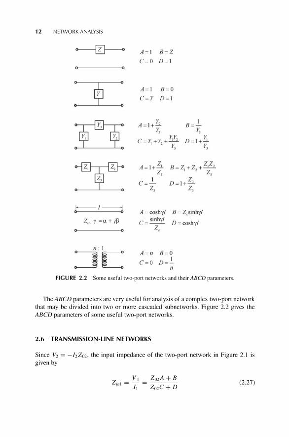
FIGURE 2.2 Some useful two-port networks and their ABCD parameters.
The ABCD parameters are very useful for analysis of a complex two-port networkthat may be divided into two or more cascaded subnetworks. Figure 2.2 gives theABCD parameters of some useful two-port networks.
2.6 TRANSMISSION-LINE NETWORKS
Since V2 = −I2Z02, the input impedance of the two-port network in Figure 2.1 isgiven by
Zin1 = V 1
I1= Z02A + B
Z02C + D(2.27)