microstrip technology and its application · c. realizations using microstrip components. 60 1. ......
TRANSCRIPT

Reproduc~d by __ . __
NATlONAL TE --IINFORMATlONC~NICAlUs Department of C RVICE
Springfield VA ;2i5'rerce
University of AlabamaBureau of Engineering Research
UniversitYt Alabama
MICROSTRIP TECHNOLOGY AND ITS APPLICATIONTO PHASED ARRAY COMPENSATION
Prepared by
James E. DudgeonProject Director
and
William D. DanielsResearch Associate
January 21 t 1972
Technical Report Number 2Contract NASS-25S94
Submitted toGeorge C. Marshall Space Flight.C~nter .
National Aeronautics and Space AdmlnlstratlonHuntsville t Alabama
(Alabama88 pCSCL 09E G3/10
(iASA-CR-123819) MICROSTRIP ~ECHNOLOGY ANDITS APPLICATION TO ~H~SED ARRAY
,COMPENSATION J.E. Dudgeon, et aluniv., University.) 21 Jan. 1972
I ~ ..
N73-11222
Unclas .J46393
https://ntrs.nasa.gov/search.jsp?R=19730002495 2018-07-11T08:13:00+00:00Z

(PAGES)
N1 3- I 1'2.:) 2(ACCES~iUMBER)
University of AlabamaBureau of Engineering Research
University, Alabama
MICROSTRIP TECHNOLOGY AND ITS APPLICATIONTO PHASED ARRAY COMPENSATION
Prepared by
James E. DudgeonProject Director
and
William D. DanielsResearch Associate
January 21, 1972
Technical Report Number 2Contract NAS8-25894
Submitted toGeorge C. Marshall Space Flight Center
National Aeronautics and Space AdministrationHuntsville, Alabama
No-0
:E~o...>...:::;~ (NASA CR OR TMX OR AD NUMBER)...

TABLE OF CONTENTS
~IST OF FIGURES
ACKNOWLEDGEMENT
Pageiii
vi
Chapter
III. MICROWAVE INTEGRATED-CIRCUITS TECHNOLOGY
II. MICROSTRIP ANALYSIS TECHNIQUES
B. Iteration Techniques .(Microstrip Characteristic Impedance)
C. Variational Methods .(Microstrip Characteristic Impedance) .
1
7
7
16. . 20
21
2425
2627
28
30
313334
3536
39
40424445
. ,
INTRO DUCTI ON
A. Lumped Element Design.
1. Ribbon Inductor.2. Spiral Inductor.3. Capacitor ....
A. Conformal Manninq . . . . .
1. Microstrip Characteristic Impedance ~
2. Coupled Microstrip .3. Coupled Stripline .
B. Distributed ~lement Desiqn(Micro$trip) ....
C. Production Techniques ..
1. Metalization Schemes2. Dielectric Films3. Substrate Properties4. Thick Film Processing
1.
i

CONTENTS (Continued) Page
5. Thin Film Processing 46
IV. ARRAY IMPEDANCE MATCHING . · · · · · · 48
A. Interconnecting Circuits Effects 52
1. Phasing . . . · · · 522. Equivalent Admittance · 543. Beam Steering · · · · 554. E, H, and D, Plane Scans ·
B. Realization of an Impedance Match 56
1. Input Impedance Variation · 572. Smith Chart Analysis · · · · · 583. Implementation · · · · · · · 59
C. Realizations Using Microstrip Components . 60
1. L-C Ci rcuits 602. Modulized Values · · · , 62
D. Interdi gita1 Capacitor 62
V. POWER LIMITS AND WIDE-RAND BALUN FEEDING OF A SPIRALANTENNA . . . . 66
A. Power Limits .
1. Voltage Breakdown2. Current Limitations3. Example ....
B. Balun Feeding of the Spiral Antenna
1.2.3.
REFERENCES . .
Coax T-Line Balun ....Microstrip Bawer Balun.Coupled Microstrio Balun.
. . . . . . . . . . . . . . . . . . . . . . , .
ii
68
697172
73
737677
79

~IST OF FIGURES
Even and Odd-Mode Impedance for Parallel-CoupledMicrostrip Transmisslon Lines (81=9.5) ... ' .. 20
~ven and Odd-Mode Impedances for Paralle+-CoupledStripline . . . . . . , 21
Fi gure
2-3
Title
Complex Plane Geometries .
Page
9
Stripline"Charatteristic I~p~dance with Thicknessof Conducto~ as a Parameter . . . . . . . . 23
2-4
2-5
Geometry of Eq. 2-63 .... . . . .,. . 21
2-6
2-7
Characteristic Imp~dance of Microstrip withExperimental vs. Theoretical Curves 22
Microstrip Characteristic Impedance Solved UsingGreen's Method. . . . . . . . . . . . . . . .. 25
Correction Factor K as a Function of wit 32
Lumped Spiral Inductor 33
Ribbon Inductor in Free Space 31
Coplanar Waveguide Construction 30
34..
Characteristic Impedance for Various DielectricConstants of Microstrip 27
Slot Line Construction. 30
Lumped Element Capacitor
Microstrip Transmission Line. 36
Transmission Line with Series-Inductance LandResistance R per Unit Length, and ShuntCapacitance C and Conductance G per Unit Length. 37
2-8
3-1
3-2
3-3
3-4
3-5
3-6
3·,]
3-8
iii

Figures (Continued) Title Page
Dielectric Cover Sheet a Distance d Above ArraySurface . . . . . . .. 49
• • • t
3-9
3-10
3-11
3-12
3-13
4-1
Filling Fraction of Microstrip vs. Strip widthOver Substrate Thickness ...
~ayers of Metal in a Chemical Bond .
Layers of a Chrome-Silver-Gold Metalization
Plating-Etching Process
Etching Thick Metal Process
38
39
40
45
46
4-2
4-3
Array Modules for Use in 60° Triangular Grids.. 51
Shunt Admittance Interconnection of AdjaGentArray Elements .. ~ ... , . . . , .. , 52
Array Geometry Giving Angle Criteria. 56
Variation of the Input Impedance of a CentralElement of a 61-Element A/2 Dipole Array Overa Ground Plane 57
4-.4
4... 5
4-6
4-7
4-8
Equivalent Admittance to Ground
Plot of Sin2 (8/2) ...•...
Graphical Analysis of Impedance MatchingTechnique . . . . . . . . . . . . . . .
54
55
59
4-9
4-10
4-11
4-14
4-13
Equivalent Circuit for H-plane Scan ImpedanceMatching of an Array Characterized by DataGiven in Fig. 4-7. . . . . . . . . . . . . . .. 59
Propertt~s:of a Circuit with Parrallel L/and.C. 60
Frequency Characteristics of a Series L-CNetwork . . . . . . . . .. 60
Interdigital Capacitor for Use in Modular AntennaElements. . . . . . . . . . . . . . . . 62
The Interdigital Capacitor on Dielectric ofThickness d Above a Ground Plane. . . . 62
4-14 Equivalent Circuit for the InterdigitalCapaci ty .... . . . . . . .
iv
. , . . 63

Figures (Continued) Title Page
4-15 Computational Graph for-D~terfuin~tion 6f-~1 arid"A2given the Dielectric Thickness d and FingerSeparation X. . . . . . . . . . . . . . . . 63
5-1 Characteristics of an Archimedian Spiral AntennaDesigned with a Center Frequency of fb . . . .. 67
5-2 Variation of Breakdown Voltag~ vs. ConductorSp~Ging as a Function of Frequency 69
Graphical Interpretation of Eq. 5-9 with XL = 0and 61 =,62 = 6.. Frequencies f l and f2 Correspondto Solut1ons of sln26 = Zin/RL . . . .. . . .. 75
1.5 Turn Archimedian Spiral Antenna
Maximum Current Capability of Copper Hire
5..3
5-4
5-5
5-6
\~i de Band Bill un • • • • • • • .• l! • • • ~ •
70
72
73
Bawer and Wolfe Printed Circuit Balun .. ~ . . . 76
Characteristic Impedance for a Two-Ribbon BalancedLine . . . . . . . . . . 76
5".9
5-10
Coupled MicrQstrip Balun
90° Broad-Band Phase Shifter
v
, ...
78
78

CHAPTER I
INTRODUCTION
This report is a systematic analysis of mutual coupling compensation
using microstrip techniques. A method for behind.the-array coupling of
a phased antenna array has been reported by Hannan [13J and this method
is investigated as to its feasibility. Beginning with a detqiled
review of microstrip transmission line parameters and fabrication
techniques this report trys to prepare the reader fo an in-depth real
ization of Hannan's procedure using typical component values. The
matching scheme is tried on 'a rectangular array'of'A/2" dipoles', but:~it
is not limited to this array element or geometry. In the example cited
the values of discrete components necessary were so small an L-C
network is needed for realization. Notice that such L-C tanks might
limit an otherwise broadband array match, however, this is not significant
for this dipole array. Other areas investigated were balun feeding and
power limits of spiral antenna elements. Hannan's method requires a
knowledge of the parameters of each element in an active array environment.
Experimental attainment of these values could be expensive whereas computer
simulation would be quick and precise. This method is not cost competitive
with some of the matching schemes such as dielectric cover sheets, however,
future advances in batch processing may amend this. Assuming adequate
precautions, post processing would lower cost by increasing yield. The
redeeming feature of this method is its theorethical ability to match
preciesly every element individualy, whereas the other wide angle1

2
impedance matching techniques attack the problem macroscopicly.
Chapter II delves into the theory and realizations of stripline and
microstrip. These transmission lines have been widely used in industry
andn.n· abundance of information on thein-is·aVailable ih literature
Other types of transmission lines presehtlyurider·~t~dyare· the co~lanar
wave guide and slot line. These t-lines would allolt! shunt mounting
of devices without drilling holes in the substrate. Stripline (known
as slab line or triplate) is constructed of a dielectric supported center
conductor sandwiched between two ground planes and is thus self
shielded. Microstrip which consists of a ribbon conductor over a
ground planes is not self shielded so it is usually enclosed in a
~etal box to curb radiation exchanges. The parameter of characteristit
impedance is considered in detail and sufficient information is
included for any design implementation. In the propagation of quasi-
TEM waves, because the fringe fields above the microstrip are in air
which has a relative permittivity of one, the conductor supported by a
dielectric appears to have an effective dielectric constant lower than
the value for the dielectric. The phase velocity and characteristic
impedance of stripline are functions of the dielectric in which the
conductor is embeded. Microstrip properities are determined by a
knOll/ledge of E;I • the effective value of the dielectric constant.r
The fields of closely spaced t-lines interact producing a mutual
coupling which has found uses in filters, delay lines, and directional
coupler. Graphs are illustrated which allow the interpolation of
characteristic impedance for even and odd mode couplinq. The majority
of the developments in Chapter II pertain to microstrip because it

3
s~ems the most likely candidate for integrated system work at microwave
frequencies. Active devices and passive systems can be built directly
into the microstrip. Microstrip requires less area and is less-expensive
to fabricate than the alternate transmission line realizations.
Chapter III presents some techniques for microwave integrated circuit
design and fabrication. Substrates, conductors, and dielectrics
are evaluated and conclusions as to the most optimum choices are stated.
Presently elements for microwave circuits are cate90rized as either
lumped or distributed. Lumped element performance is independent of
frequency over the range of interest while distributed elements are
sensitive to frequency. The lumped element approach is best suited
to direct, electrical coupling between adjacent antenna elements
because it is frequency independent and assures braodbandness in
impedance matching. For an element to remain truly lumped its
circuit components must be electrically much shorter than a wave-
length so for the frequency range of interest the geometry is
minute. Because of the simple formulations for finding inductance
values (purely geometric: a ribbon of conductor in free space)
and capacitances (proportional to area for a given separation and
dielectric constant), the lumped element design is largely concerned
with fabrication guidelines for the devices. Photolithographic
fabrication has made it possible to produce lumped elements to
X-band and lower Ku band. These lumped elements because of their
size, can be reproduced inexpensively with many circuits on a
single substrate. Lumped element MIC's are readily compatible with
solid-state devices. Alunmina (A1 203) has become a widely used

4
substrate because it has a low loss tangent and high dielectric constant
(order of 10). Pure sapphire would be preferred since its loss tangent
is lower, but it is fairly expensive. In order to reduce line losses
further the conductor should be chemically bonded to the substrate.
A mechanical bond requires a rough substrate which will increase lin~
loss. Two production techniques for lumped and distributed elements
are reviewed. Thin film processing which allows very high resolution
on the etch of the pattern has a lower dc resistance than the thick
film method. Hith thick film processing, however, capacitors capable
of handling high voltages and having no pinholes are easier to make.
Microwave resistors result from films and conductors of known sheet
resistance. The quality factor of the lumped elements decreases
greatly at frequencies above 8 GHz with present technology,even
though higher QI S are predicted by theory. The total Q is dependent
on the conductor Q and the dielectrics loss tangent (i.e. zero loss
tangent implies infinite Qd)' Two approaches to fabrication of these
circuits are hybrid and monolithic integration. In the monolithic
circuit active elements are grown epitaxially in pockets of the
substrate. To date silicon has proved unsucessful as a substrate
because it fails to keep is resistivity. Galium arsenide would be
a better choice, but the technology involved with monlithic fabrication
is furturistic.
The intent of this report is to investigate all facets tif Hannan1s
method for wide scan impedance matching a planar phased array. Chapter
IV is concerned with a metbod to effect impedance matching through
behind-the-array interconnecting circuits. The hybrid combination

5
of lumped and distributed elements would be the most ootimum approach
to realization. Here, the lumped elements would be used to realize the
behind-the-array mutual coupling and the distributed or microstrip
transmission line will connect these circuits to ~he antenna elements.
The method of Hannan~for~ihterconnettinqtircaits~isadopt~d arid~t~js
method is compared with other schemes for array matching. The dielectric
cover sheet utilizes mutual coupling to effectively connect every
element of the array and if properly designed allows an approximate
impedance match. An example is worked out using Hannan's procedure and
once the values of the components are determined, their fabricatiQn
is oi$cussed as to feasibility. Once the circuits are produced there
may arise a need to tune and fine adjust them. Initial design should
allow for post fabrication improvements. Some of these are micro
cantilever for tuning microstrip and trimming metal from lumped
elements. The optimum array geometry in terms of aperture size per
number of elements if the triangular grid. Six interconnecting
circuits would be required qS opposed to only four for the retangular
geometry, however, there is no appreciable difference in the matching
requirements if a dielectric cover sheet were used.
Chapter V deals with fabrication problems, balun design, and power
limits associated with spiral antenna elements. Because the spiral
antenna which is a balanced, symmetrical structure is to be fed with
microstrip, an unbalanced transmission line, and interface between
them is needed. Assuming the spiral antenna is to be used in a
wideband mode, the interface is hopefully frequency independent.

6
This chapter describe$ two different baluns which are applicable to
the spiral. The Bawer balun is commonly used in cavity-backed spirals,
while a balun which employs coupled microstrip phase shifters seems the
best suited for Ku-band spiral arrays because its ground plane can
serve as the spiral's ground plane. Also the later balun provides
matching at the center frequency whereas the Bawer ba~un does: nato
Tr~e maximum power the antenna can radiate was investigated. A
value of four watts "rms per element is cited considering a large
safety factor. For spacecraft applications a thin layer of dielectric
might be used to cover the spiral's surface to prevent voltage breakdown
between the conductors since the breakdown in air is a function of
pressure and ion density. At the frequencies considered it is concluded
that the antenna is capable of radiating as much power as the sources
can provide.

CHAPTER II
MICROSTRIP ANALYSIS TECHNIQUES
The use of microstrip and striplines in low price cir,cuits of
high reliability obviously requires knowledge of their microwave
parameters in order to realize their design. This section is conc~rned
with three methods of obtaining the capacitance associated with their
geometries. For reliable conclusions it is necessary that for iden~
tical geometries the three different analytic methods yield the same
or very close results. If the capacitance of a geometry is known,'the
characteristic impedance of the transmission line can be found if the
effective dielectric constant of the separating medium is known.
Mutual coupling between these lines is specified if it exists. The
three methods to be discussed are: conformal mapping, iteration
techniques, and variational methods.
A. CONFORMAL MAPPING
A review of complex variables will serve as foundation for the
following. Afunction ~(w) of a complex variable w = u + jv is called
analytic within a region R if the derivative
d~(w) =dw
1im L\~L\W -+ 0 L\w
exists within R independent of the direction chosen for L\W. The
necessary and sufficient conditions for the above to hold are known as
7

8
the Cauchy-Riemann conditions. For
~ = ~ + j~ (complex potential)
w = u + jv
the Cauchy-Riemann conditions are
Now
a~ a~- =au av
a a~- =au au
aeI> a~
- =qV - au.
a a~ a2~ d2~= -~ = -;;av av auav
Substituting (27Z) in (2~3 ) gives Laplace's equation
A similar procedure will show that both ~ and ~ are solutions to
Laplace's equation. Thus we call ~ the complex potential. eI>(real part
of ~) are the lines of constant potential (to be shown) and ~(imaginary
part of ~) are the lines of constant field strength (electric flux).
The Schwarz-Christoffel transformation gives a method by which the
interior of a polygon -in one complex plane can be mapped onto the upper
half of another complex plane. It is given by
J3

9where
Xo = point on u-axis of w-plane corresponding to point in z-plane1
a i = corresponding to angle traversed in z-plane when xi in
w-plane is traversed.
Consider two parallel, semi infinite conductors in the z-plane.
y
°d~ (- 00 , .Jf)
a =02
v =°
i-plane. A(O,jd)0,1 = 27T
0,3 = 2'TT C(O,O)(a)
v
x
w-plane
v = Va V=°.----.......--rr~-..----~~---::!::_-"----I--__==_---_ __._ U
(b)
Fig. 2-1. Complex Plane Geometries.
From inspection of the two planes the transformation can be written
by (2-5) to be
~, 2*= A' (w+l) JW-l) = AI (w ~l) AI= Alw .. -,
W

10
z = Jdz dw = AI w2
- AI 1nw + BIdw 2"
Applying the transformation condition at point C says when z =0 w = 1
0 = ~+ BI ( 2,.8)2
yielding
BI AI( 2,.9)= -2
Applying transformation condition at point A says when z = jd w = -1
r.eal and imaginary parts must be equal
d = - Alrr
AI = _ E-1T
B' = .i.21T (2-12)
Therefore the transformation relation is complete
2d (l-w )z = -; -2- + lnw (2..13)
(2-14)
Now if the above equation could be solved for w, the problem would b~
much simplified. It would be necessary to find a harmonic function of
w, invert the expression and pll,Jg into the expression for z,_ and. then
solve for the desired quantity.
For clarity, the following example is inserted.
Example
If the transformation had yielded
z = 1Td w1/2,

11
then
'/ Z) 2w = {-\ TId ,
A harmonic function of w is
VQ = ~ lnw (after some boundary conditions applied)TI
(2~15)
Vo Z 2Q = -' 1n(........d}TI TI
2V--.Q. 1n Z - 1n(TId )TI (2-17)
2V 2Vrl = ~ 1n r + -.9. ie - 1n(TId} (complex potential)TI TI
The problem ;s then solved. Also there have been no approxi-
mations made. In continuing the first problem it wa~ shown that for
the stated geometry
. 2d (l-w )
Z = -; -2- + 1nw
This is a transcendental equation. Therefore only an approximate
solution is available. Now if we let w be expressed in polar coordinates
iew = r e
the complex potential function is
(2-20)
(2-21)
A function which ;s harmonic will by definition satisfy Laplace's
equation in polar coordinates. So if Q is harmonic then:

12
The above is ~atisfied by
n =A 1n w + a
where A and B are arbitrary constants to be determined.
n 9 A1n r + Aie + B
(~-:24)
(2-:25)
Now apply the baundary conditions to the complex potential (see Fig. 2(b))
~ =0 n =0, anqe = n
o = A 1n r + B
V = A 1n r + Ain + Bo
~ = V. 0
(2-27)
(2-28)
Substituting (2~27) and (2~30) into (2.25) yields
n = A ln r + Aie + B (2,.31)
(cQmp1ex potent i al) .
+ +
The charge Q = If D . ds ( 2-33)

13
The ele~tric field E is-+-E = - v ~
-+- 1 an 1 VoE = - ---,- ag = - --, 9. er ae r 7T
EN = 1 Vor 7T
""* -+-JJ 0 . ds = Jff p dv = Q
€ EN ds = - p ds (-p because the line integration of charge
density is over negative charg~)
, ... V_ € 0
P ---7T r
(See Fig. 2!"1(b)).
Q = J~ ( ~,V~\du'. 7T r)Xl
The charge per unit length is thus
. dl,;,w2z = -; [ -2- + ln w]
(2-34)
(2-35 )
( 2-36)
( 2-37)
(2-38)
(2-13)
The point'x=-.fin ~he'Z':'plime ma'ps to w=xl a'nd w'::;,x2 i"n the w~plane
l3ecause the'mapping':;s c'onforn\a'l'~r:an'd'wVh~'s two value's 'fo'r"each -,
'va1,ue 'o('z because: the'plcite':in' the:; z~pl ail~ 'has-)lw6"s:;'d~s of charge.
2d l-Xl
-~ ~ ~ [ 2 + ln ~l] (2740)

14
For It 1 (It 1 implies magnitude of t) very large,IXll is very small and
IX21 is very large. Because weare trying to sqlve a transcendentQ,l
equ~tion the following approximations are made when. I~I i$ very 1arge:
Xl smoll; 112 negligible + 11
2 = 0
(2"743)
Substituting (2~42) and (2~4~) into(2~40),nd (2~41) respectively
yields
d 1 .-t=;[Z+lnXl ]
Solving for ln Xl in (2~44) yields
.. t71' 1In Xl = .. d -"2
Solving for ln X2 in (2-45) yields
1 . 271'tln X2 = 2 ln [~ + lJ
Substituting (2-46) and (2-47) into (2-39) gives
vQ(L) = e: 1T 0, [1 n ~ .. 1n Xl]
(2-44)
(2.. 45 )
(2-46)
(2-48)

15v
Q(L) = s.....Q.:{ 11n [21fQ. + 1] + [!!.+ 1]}1f 2 d d 2
If we assume further that t» 1, then (2~49) will reduce to
vQ(L) = E: 1f 0 [ t ln (2dQ.) + %] (2-50)
To compare the results with a crude approximation of an infinite
parallel plate capacitor with no fringing fields we find that
(charge per unit len~th
on parallel plate capacitor)
Subtracting (2.,.51) from (2",50) gives the Ghar~e due to the fringing
capaci tance, Qf
(2-52)
The total capacitance per unit length is thus the sum of the fringing
and enclosed charge.
For a transmission line the characteristic impedance Per unit length is
V 120 = r = ur
where u is the velocity Of propagation of the wave along the line.
z =o1
1/1):1; cohms (2-55)

16
Usin9 the capacitance calculated in Eq.(2-49) and assuming we"
now have two frinqing fields, one on each side, the characteristic
imoedance of Eo.(2-55) hecomes
(377) 1
~ ! + JIln(2n£ + 1) +lJd 7T a
(2-56)
This value of Zo is valid for ratios of £jd greater than 3.0.
A closer approximation for Zo valid for £jd in the ranqe 0.1 to 3.0
is
377Zo =----:------;---;;;--:---IS C~· + 1. 0 + 1 1n (2n £ + 1))
r d n d
(2-57)
This equation is experimentally verified by the experimental data
published by Hyltim [7J (see Fig. 2-6) and is compared with Eq.(2-59) "
and Wheeler's results in Table 2-2;
The effect of the dielectric filter is an important parameter to
cons i der for di e1ectri c constants di fferent from 1. Hhee1er [1] has
$olved this problem of finding the effective dielectric constant to
be used.
E: + 12 (2-58)
Table 1 has a few common dielectric constants and the value to be used
for E: r in equation (2-57) tabulated. In the case of microstrip the
ratio of the width of the conductor (£) and dielectric thickness (d) is
also a variable which determines the effective dielectric constant E:1
•
It -t.!Jrns out that for a wi de stri 0 (£ » d) above an i nfi nite ground
plane the characteristic impedance per unit length has been shown by
Assadourian and Rimai [2J to be

17
TABLE 2..1
Dielectric Ratio EffectiveConstant Q,/d Dielectric Constant
1 1 1.000
19 1.000
2 1 1.706
2 10 1.578
3 1 2.384
~ 10 2.144
4. 1 3.054
4 10 2.708
5 1 3.721
5 10 3.271
6 1 4.387
6 10 3.833
7 1 5.052
7 10 4.395
8 1 5.716
8 10 4.957
9 1 6.380
9 10 5.519
1Q 1 7.044
10 10 6.080
11 .1 7.708
11 10 6.642

18
TABLE 2... 2
CHARACTERISTIC IMPEDANCE
Ratio Rimai [2] Wheeler [1] Daniels [xperimAntaltid
Eq.(2-59) Eq. (2-57) (Hyltin)
O. 1 491. 089 373.417 300.352 299
0\2 420.151 330.886 258.384 250
0.3 367.591 297.650 230.263 .227
0.4 327.061 270.898 209.447 206
0.5 294.835 248.859 193.101 190
0.6 268.586 230.359 179.754 176
0.7 246.780 214.588 168.552 168
0.8 228.370 200.968 158.955 160
0.9 212.614 189.076 150.600 ··151
1.0 198.971 178.954 143.235 145
2.0 122.486 116.200 98.432 107
3.0 89.337 86.903 76.143 85
4.0 70.651 69.679 62.430 70
5.0 58.593 58.274 53.044 60
6.0 50.138 50. 139 46.180
7.0 43.867 44.031 40.926
8.0 39.021 39.271 36.769
9.0 35. 161 35.453 33.392
10.0 32.010 32.320 30.593

z = 377 ohmso ~ + ~ [In[l + 2~] + lJ
19
(2-59)
In the case of a narrow strip above an infinite ground plane (d » t)
the characteristic impedance was found to be
377 -1 dZo = b cosh (Q:")'
Up until now, all formulation has been concerned with a single ribbon
conductor on a dielectric over a ground plane. Now, let us look at a
pair of conductors in what is called coupled microstrip. Judd et al.
[3J have calculated the input impedance to a pair of coupled microstrip
lines for two cases. When the currents in the lines are in phase (even
mode) and when the currents are 1800 out of phase (odd mode). Their
results are displayed graphically in Fig. 2-2 with the parameters of
line spacing and width over dielectric thickness to determine the
characteristic impedance.
The above formulation has all been concerned with microstrip. Strip.
line or sandwiching the center slab line between two ground planes
gives the transmission system a built-in shielding. Work has been done
by Cohn [4J for the case of coupled strip line. He has shown that for
the case of even mode symmetry the characteristic impedance is
30 1T
~( 2-61)
where k (ke) is the elliptic integral of th~ first kind and
k = tanh(2:. . !.) . tanh(2!.. . HS) and ke
= /1 - k 2e 2 d 2 d e

20
f-); --+-5 +-2 ~/ / t /TOT / ) /./
150 I-\-.......+---+----l--+---If-.--+--~
Sidu'r- 0.005 "~ 0 25 '" EvenI: i--~--+-~~"-l::-~~~-~~1:0 Mode
t 2.0 /~ 40 1---+-~-+--+----I~o..d----::J-2. ~~ 1.0u
30 i-----4~_I_ _ __J_--+-_+-::::::......d".__I__l
VIE~
o 100 I-lr.:l~~~--+-..-+--+--_J___f___+
90 ~~-----=~.____J--_+--+----1f--_+___t
80 I-+~~rl-~*--+----l--+--I___t
70 I--~~~ ~~--+----lf--+___j
0.25 OddMode
--~-r0.005 /20 1..-----J'-----1_--1._---l..._~_ _+_---I.___+
0.1 0.3 0.5 0.7 0.9 1. 1 1. 3 1.5 21 d
Fig. 2-2. Even- and odd-mode impedances for parallel-coupledmicrostrip transmission lines (sr = 9.5).
For the case of odd mode symmetry
k = tanh (E.. .!) coth (211" • 2+dS) •o 2 d
('2-62)
Because the elliptic integral is a tabulated function,graphs of
solution are possible.
Hilberg [5], following a similar manner, has computed even and
odd mode Zo and his results compare almost identically with those of

21
160......II
>-w 140tilE
..s:::;0 120
0N
OJ 100us::: 4co l S-J"'0 dOJ 80 -~ ~t-"l0-
*E......u 60'r-+-'til
'r->- 40OJ+-'Uco>- 20co
..s:::u . 1 .15 .25 .4 .6 1.0 2.0 3.0
Q,/d
Fig. 2-3. Even- and odd-mode impedances forparallel-coupled stripline.
Cohn. Hilberg's results, however, include a wide range of values for
Q,/d ranging up to 100 and down to 1/1000. Hilberg's generating
functions are
2 ~inh ~ / sinh ~ + 1
/ TIU2 TIU,Vsinh h / sinh -h- - 1
(2- 63)
Fig. 2-4. Geometry for Eq. 2-63.

22To determine Z·even replace all sinh(x) by cosh(x) in Z:odd'
Cohn also included a very useful nomogram from which design of a
stripline can b~ m~de for a desired zoo
Bates [6] used conformal mapping to determine the characteristic
impedance of a shielded slab line but he took it one step further by
considering the thickness of the line. His results are in the form of
a useful design graph. (See Fig. 2~5).
In the case of microstrip on semiconductor (Si) Hyltin [7] con-
ducted experimental verification of calculated values ofZ o for
€r = 11.7. He compared his results with Assadourian and Rimai and
there is a definite difference, however when compared with mY results
his experimental and my theoretical results are extremely close.
4-300
1) A&R250
OJ 2) Experimentalucto
E: r=11·7-0 200OJ0..E
~~ 3) Experi menta11-1
u 150......~ 0
s =8.9VI N...... r~OJ~ 100 4) Danielsuto~ ...to .)
Eq. (2-57)..s:::u 50
0.1 002 0.5 1.0 2.0 5.0 10.0
9../d
Fig. 2-6. Characteristic impedance of microstripwith experimental vs. theoreticalcurves.
c

LaiIi
I,
Ii
IIiii
\,
,t
I
I~'I
-r-t~----r--I---_..·-
t--
---0
.8~-
-L~+
-=::
::::
~:::
-r-j
-l
I----l-
-
t IT
kJl ..,
!.
I
04
SiLl
•.
''f'
"dL
_I
---r
--1
-1-
1 1
'-0'2
l\~,}:
:~I'~t
~l~~t"
,::::j
~~+,~~
:::::~
~J-_l~
.~~~~~LctI:
N W
1.6
1.4
1.2
1.0
0.6
004
0.8
~d
Str
ipli
nech
arac
teri
stic
impe
danc
ew
ithth
ickn
ess
ofco
nduc
tor
asa
para
met
er.
0.2F
ig.
2-5.

24
B. ITERATION TECHNIQUES
The important concept to realize here is that many different types
of cqmplicated geometries can be solved quickly by this method on a
digital computer. The theory behind the program is that a Taylor
series expansion can be made of the potential function about a point.
x=a
V(x) = V(a) + (x - a) aV(x)ax
2 2/ + (x-a) a V(~) / +2:
ax x=a
It should be noticed if the expansion about a = 0 of V(x) in the +X
direction ;s added to a similar expansion in the negative x direction,
the result will yield a term a2v/ax2. If the same technique is used in
y directions a2v/ ay2 will be obtained. The sum of these will yield
Laplace1s equation which must equal zero in the charge free region.
Of course, appropriate approximations must be made. A conditional
result ;s that the distance between the test points must be small com
pared with the geometry.
For every point an eq4ation will result. Thus the problem is to
solve a number of simultaneous equations. Green [8J used a method
known as sUGcessive over relaxation to solve these equations. Use of
the equation
V. (j+l) = V. 0)-1 1 .
r.!a ..lJ
n
~ ai k Vk ,(j) - bik=l
(2-65)
where AV = B

25
a. k, v., b. terms of matrices A,V,B, , ,j::; number of i terati on cycl es
n;:: number of simult~neous equations
n= accelerating factor (best n = 1.95)
This m~thod ¥ields values corresponding to one set of input data
as opposed tQ the functional equations yielded by conformal mapping.
Green's results published in the form of a graph (see figure) compares
favorab lY wi ~h my ana lyti c res\.Ilts.
\
\ r=2. (5
\
1\ rh;:l I'acter .sti c
~-1 npedan r--e
\'I
1\I\.
'\~.'\ Vel pcityI'.. Rat io - V
~R:V
~
~ i::::
120
110
III 100E..c:0
s::..... 90Q)us::1'0 80'"0Q)0-E.....u 70
.....of-)III.....
60s-Q)
of-)U1'0s- 501'0
..c:u
40
30o 1 2 3
Md4 5
0......78 of-)
toe:::
~.77 .....
u0.....(1)
.76 >
·75
.746
Fig. 2-7. Microstrip ~harqcteristic impedancesolved using Greens method.

26
C! VARIATIONAL METHOD
The solution of Poisson's equation
when inserted into
1 1Co = Q2 J p (x ,y) <P (x ,y) dS
s
(2-66)
(2-67)
gives the capacitance of the geometry whose boundary conditions were
used to solve the 9ifferential equation. For the case of the infi
nitely thin strip the charge d~nsity m&y be expressed as
p(x,y) = f(x) 8(y-b) • (2-68)
If the Fourier trqnsformation of <p and f are taken and inserted into
the function of capacitance
00
1 =Co 21T~2 f ((B) I(p,h) dB
_00
(2-69)
If this expression can b~ evaluated, the characteristic impedance can
be d~termined from
z =o (2-70)
Yamashita an9 Mittra [9J evaluated this expression for capacitance
on a digital computer. They used for f(x)
f(x) = Ixl
x in the rang~ of the strip width.
(2-71)

27Their results are displayed graphically and compare with my
results and Wheeler1s results favorably. They also have graphical
data for the cases of finite thick slab above ground plane.
200
100
I) k:l:: 'lfl.O
~ '\4 ~ 1\ 1\
"' '\ \1\ 1'\ 1\-8 ~ '"~t'- "~ \1 f'.,
~ ~ 1\"-l'l t'-... "\.,-v
"- ~~ r'
,t'--~ r:: ~f\r--- t--... "'- I:'.. ['.. "-
E: : 5 I'-::::... ~~~ ~- r-. ~r t- t- ~~r-- r-::: I§~
10-1 1tid
10
Fig. 2-8. Characteristic impedance for various dielectricconstants of microstrip.

CHAPTER III
MICROI~AVE INTEGRATED-CIRCUIT TECHNOLOGY
In this chapter some of the basic design and fabrication methods
applicable to microwave integrated circuits.are discussed. Some good
survey papers [11,18,19J exist on the topic, and these are referenced
freely. Presently elements for microwave circuits are categorized as
either lumped or distributed. With lumped elements, performance is
independent of fr~quency over the range of interest while distributed
circuit elements must be treated with transmission line techniques
and have element values which are sensitive to frequency and line
length variations.
Lumped elements are physically small compared to a wavelength, and
as long as this constraint can be met, it is possible to obtain element
values which are independent of frequency and behave pretty much as
their low frequency counteroarts. Lumped circuits are flexible in that
they can be designed so that element values can be changed after the
device has been fabricated, a feature not so easily accomplished with
microstrip circuits. Lumped elements are amenable to batch processing
and with present technology and fabrication procedures are practical
through 12 GHz and feasible to even higher frequencies (20 GHz).
According to Caulton et al.[19] they are currently very competitive
with microstrip through 6 GHz from cost, size, and design complexity
28

29
considerations as evidenced by the following commercial lumped element
devices:
(1) S band amplifiers (expecially suited for high power
designs) 6 watts cw, 26% efficient, 35 db gain,
2.25 GHz transistor amplifier.
(2) C-band impedance transformers built and t~sted
(3) Filters and quadrature hybrids.
As element size becomes an appreciable fraction of a wavelength,
lumped devices look more and more distributed. This and the increase
in parasitic effects with frequency set the upper frequency limits for
lumped elements. It has been reported [19J that single turn inductors remain
truly "lumped" to about 12 GHz. Multiturn spiral inductors which have
potentially higher QI S than single turn inductors begin to suffer from
interturn capacities and distributed effects earlier and their useful-
ness is limited to about 6 GHz. Also because of the interturn capacities,
the maximum achieveable resonant frequencies for multiturn spiral
geometries are lower than for single turn. Using thin film technqiues
lumped capacitors having QI S from 600 to 5000 can be constructed with
values typically ranging from 0.1 to 50 pf. Capacitors easily remain
1I1umped" for frequencies up to 12 GHz.
Distributed circuit element realiz~tions-at'~icrowave~frequen~ies
are possible using microstrip, slot line, coplanar waveguide, and
~tripline. Microstrip will be emphasized in this discussion because
of its widespread adoption by users. It consists of ribbon conductors
separated by a dielectric substrate from a conducting ground plane.
The fields propagate with a quasi-TEM mode, and a detailed analysis

30
of their behavior is given in Chapter II. Two additional ways of
realizing distributed circuit performance, slot line [20J and coplanar
waveguide line [21J, are shown respectively in Figs. 3-1 and 3-2.
Substrate
Fig. 3-1. Slot Line Construction. Fig. 3-2. Coplanar Waveguide Construction.
Both have the advantage of allowing shunt mounting of devices without
the need for drilling holes in the substrate, but neither are widely
used yet.
A. LUMPED ELEMENT DES IGN
For an element to be truly lumped its electrical length must be
much smaller than a wavelength or the element would introduce a
terminal-to-terminal phase difference. Therefore, it is obvious that
when the operating frequency is Ku band (12-18 GHz) the lumped circuit
elements are extremely small. The development of photolithographic
technology has made it possible to fabricate these small circuits
inexpensively and reliably. Because the operating frequencies are so
high the values which must be realized are small, for example an
inductor of a few nanohenrys is all that is required.

31
In the case of a capacitors 50 picofarads is a large value and
even this is easily realized. The formulas to compute the values of
these lumped elements are classical and are approximates but they
yield values which are close enough. The formula for a ribbon inductor
(see Fig. 3-3) is [10]:
L = 5.08 X lO-3.Q, [In w~t + 1.19 + 0.22 w;t ] (3-l)
where
L = inductance in nanohenrys
w =width of inductor in mils
.Q, = length of inductor in mils
t = thickness of inductor in mils
Fig. 3-3. Ribbon Inductor in Free Space.
The ratio of the stored energy to the average power loss in an element
is called the quality factors Q. The unloaded Q of the ribbon inductor
is
Q = wLR (3-2)

32
where R is the high frequency resistance of the ribbon and is expressed
as
KR £ •_ sR - 2(w+t) (3-3)
Kis the correction factor and is plotted vs. wit in Fig. 3-4 and Rs
1.8
K1.4
1.0 ,I1 2 10 100
';J/ t
Fig. 3-4. Correction Factor K as a Function of wit.
is the sheet resistance in ohms. For copper, Rs is 2.61 x 10⁻⁷ fl/2
(see Table 3-1). In order to obtain higher inductive values while
conserving chip area it is standard to use a spiral ribbon induct9r
(see Fig. 3-5). Because of mutual coupling, the formula for computing
the values is [10J:
2 2·n (do+di )
L = 32(d +d.) + 88(d -d.) nanohenrys (3-4)o , 0 ,
where
n = number of turns
d = outer diameter in milsod. = inner diameter in mils.,

33
w»s
Fig. 3~5. Lumped Spiral Inductor.
The Q of the spiral inductor is
8f LwQ = K1R n{d +'d.)so,
(3 ...5)
There exists an optimum value for the ratio of do to di , and it turns
out that for do = 5 di , the Q of the spiral inductor is highest. There
must be some space, di , to allow lines of flux to pass through the
center in order to increase the stored energy per unit length. Also
the spiral arms should be kept as wide as possible with the space
between the arms kept-large enough to avoid parasitic distributed
capacitances. The use of a square coil increases the inductance per
unit area, but its Q is less than that of a spiral inductor. In the
case that the inductor is above a ground plane the ratio of dielectric
thickness to conductor width should be gr~ater than 20 [11J in order to
avoid parasitic effects.

34
The lumped element capacitor is realized by the classical meta1
dielectric-metal sandwich-and-its·va1ue; neglecting fringing fie1ds,~$s
given by
E: =E: =r
E: =a
c = .e.d
relative dielectric constant
5.7 x 10⁻¹¹ farads/em
(3-6)
S = surface area of the top metal (i x w)
d = distance separating the top meta1 from the ground plane.
DielectricMeta1~:::~fcl~~~~~~Substr~te
TopMetal
Fig. 3-6. Lumped Element Capacitor.
The Q of the capacitor whereS is square (1 = w) is given by
Q =
where
(3-7)
(3-8)

tan 8 = 2nfso
35
(tan 8 is the (3-9)dielectric loss tangent)
The microwave lumped resistor is obtained by depositing a thin
film of metal where its value is the sheet resistance of the metal.
However, the input impedance to this resistor must take into account
the capacitive value of the metal film. Thus the impedance of this
resistor where R »wL is:s
z. =ln w . . wCRs~+ J--Q, 3
(3-10)
In all the cases of lumped elements the metal film thickness should
be at least 3 skin depths where the skin depth, 0, is given by
°1 (3- 11 )=
Inff,l0
f,I = permeability of metal
0 = conductivity of metal
f = frequency of operation.
B. DISTRIBUTED ELEMENT DESIGN (Microstrip)
Microstrip circuit design is a distributed element approach and
probably has the edge over lumped elements for Ku-band and above with
present fabrication technology. Microstrip is an unbalanced trans
mission-line structure which is constructed as shown in Fig. 3-7. A
high dielectric constant substrate is coated on one side with a ground
plane conductor, and a ribbon conductor whose width and height above

36
the ground plane for a fixedsubstrate·dielectric constant can be
varied to control line characteristic impedance. The electromagnetic
Fi g. 3-7.
Substrate Ground========~:.r-- Pl ane
Microstrip Transmission-Line.
propagation along the microstrip circuit is quasi-TEM with fringe
fields extending beyond the conductors. This changes the dielectric
constant of the substrate·to some effective value, a trade off between
air and the substrate (see Table 2-1). For this reason, the packages
are not as small as you would expect and in all cases are much larger
than lumped element design. However, distributed-element design has a
better reproducability than lumped element. The distributed-element
network parameters·are per unit length with the usual quantized
transmission-line model shown in Fig. 3-8.

37
~~.--,----r- ...1~--,-d_X__-'-_---L ••••
G
Te ...~ -
I ~
7. ... • •••-'11
Fig. 3-8. Transmission ~jne with Series-Inductance L and Resistance Rper Unit Length, and Shunt-capacitance C and 60nductance Gper Unit Length.
In order to adjust complex impedance values, the line lengths can
be varied. At a fixed frequency, the value for the input impedance to
a distributed transmission line system is given. by the transformation:
where:
Z.1n
ZL + j Zo tan 8L= Zo Zo + j ZL tan 8L (3-12)
Zo = characteristic impedance of the line (Eq. 2-57)
ZL = load impedance
8 = 2n/A (A = wavelength on line)
L = length of line ~
To realize shunt inductors and capacitors with distributed elements, open
. and short circuited stubs are commonly used. When microstrip is used,
the circuit losses present will be due to dielectric and conductor 10s~es
and the surface roughness of the substrate. Dielectric loss is given
by [12J

38
(3 ...13)
ad = dielectric loss in nepers per unit length
q = filling fraction (see Fig. 3~9) [1]
£r = relative dielectric constant of the substrate
£~ = effective dielectric constant (Table 1-1)
tan IJ! =dissipation factor of substrate (typical value for A1 203 is0.0001 @10 GHz)
AO
= free space wavelength
1.0
0:9
0.8q
0.7
0.6
0.5o 0.1 1.0 10 ~
witFig. 3-9. Filling Fraction of Microstrip vs. Strip Width over Substrate
Thickness
The conductor losses can be found using:
a =C
62.8 /fPI o w (3r14)

39
Z = characteristic impedance of microstrip (Eq. 2-57)o "w =width of the conductor
f = frequency in GHz
p = resistivity of the conductor
When evaluating the losses due to surface roughness just consider that
smoother surface finishes have lower losses. Production technology is
the limit to minimizing"this loss factor.
C. PRODUCTION TECHNIQUES
In order that the losses due to surface roughness be minimized, it
is necessary to polish the substrate surface to a fine degree (2 microns
or better). There are two ways metal can adhere to the substrates, by
mechanical"bond oY'chemica1bond. For there to be a mechanical bond
the surface is necessari1y"rough, so chemical bonds are required from a
loss consideration"in MIC devices. Experimental evidence indicates
that the best procedure in making a chemical bond is to evaporate ao
1ayer of chrome 50-400 A thi ck or another reduci ng materi a1 onto the
surface of the heated substrate and allow a chrome-oxide bond to form.
Then another layer of pure chrome is evaporated and any good metal will
adhere to this outer layer of pure chrome.
Typical Thicknesses511m -----,.~~:-:-;-:-:7.l
. 1pm-__~~~~~~r--o
50: A-~=====~~~:....----(
Fig. 3-10. Layers of Metal in a Chemical Bond.
bond

40
A very good combination-of metals is the chrome-silver-go1d chemical
bond.
Fig. 3-11. Layers ofa Chrome-Silver-Go1d Meta1ization.
In Cr -Ag - Au metalization chrome which adheres to the substrate is
initially applied. The" int~rmed;ate vaporization of silver is used to
separate the gold from the chrome preventing the occurrence of Cr - Au
intermeta1lic solid solutions which are difficult to etch and also the
Cr - Au combination at high temperatures causes an increase in
resistivity resulting in a loss in RF power. The gold outer layer is
employed as a nonoxidizab1e bonding surface. The Ag-Au layers which
make up the current carrying portion of the meta1ization system have
greater atomic'masses s greater activation energies for self-diffusions
and higher melting points than does aluminum. Obvious1ys the gold
system is preferred toothermeta1ization schemes for 'a-pp1icati0n'
where' a hi gher, current carryi ng 'and· thusnm"e,r handling,:capabi 1i ty
;-5 desired. If aluminum were used, the current dens.ity would be .
limited to less than 1Q6amperes/cm2 at e1evated·temperatures due'. .,..., . . .
to e1ectr~m;gration.

41
There are several other metal combinations which can be used
effectively such as:
Cr - Cu - Au
Cr - Cu
Cr - Cu - Ni - Au
Ti - Pd - Au
Ti - Pt - Au
Ta - Au
Tantalum or Titanium can be used as an alternate adhesion layer while
copper is an alternate surface layer. Copper is binded using soldering
techniques. The bulk characteristics of a few conductors are given in
Table 3-1 [18].
Table 3-1PROPERTIES OF METALS FOR MIC APPLICATIONS
Melting Skin Depth Surface CoefficientPoint (lil))) @ Resistivity vf.f of Thermal
Materi a1 °C 2 GHz rI/sg. x 10-7 f EXjansionaT C x 10-6
Ag 961 1.4 2.5 21Cu 1084 1,5 2.6 18Au 1063 1.7 3.0 15Al 660 1.9 3.3 26Cr 1860 2.7 4,7 9Ta 2980 4.0 7.2 6.6Ti 1670 10.5 16. 1 8.5
Adherenceto Film orSubstrate
PoorVery poorVery poorVery poorGoodGoodGood

42
The metalization system best suited to the job should be chosen
considering:
(1) Passive elements required
(2) Environmental and processing temperatures
(3) Compatibility with active devices.
Tantalum has been used effectively to realize capacitors, resistors and
interconnections, Tantalum1s high melting point makes it desirable for
realizing high power elements. Tantalum also offers the property that
it can be anodized to form dielectric films, When sputtered on to the
substrate it forms resistive films. The properties of other dielectric
and resistive films are given in Tables 3-2 and 3-3 respectively [18].
Table 3-2
DIELECTRIC FILM PROPERTIES
Relative Dielectric Dielectric Strength MicrowaveMaterial Constant, Er VjCM Q
Si02 (evaporated) 6-8 4 x 10⁵ 30
Si02 (deposited) 4 107 20-5000
A1 203 (anodized106or evaporated) 7-10 4 x
Ta205 (anodized106or sputtered) 22-25 6 x < 100

43
Table 3-3
RESISTIVE FILM PROPERTIES
Low TemperatureResistivity Coefficient·of
Material Q/sguare Resistivity Stabi 1i ty(oJ orc)
Cr (evaporated) 10-1000 -0.1 to +0.1 Poor
NiCr (evaporated) 40-400 +0.0002 to +0.1 Good
Ta (sputtered in anodtzed- 5-100 -0,01 to +0.01 Excellentnitri de)
Cr-SiO (evaporated or to 600 -0.005 to -0.02 Faircermet)
Ti (evaporated) 5-2000 -0.1 to +0.1 Fair
A good substrate should have the following general properties:
(1) low loss for the operating frequency
(2) chemical adherence for conductors
(3) smooth surface
(4) retain above during processing
(5 ) amenable to cutting and drilling,
Some of the commonly used substrates along with their x-band characteris
tics are listed in Table 3-4.

44
Table 3-4
PROPERTIES OF SUBSTRATES
Los s Tangen4@Er
Thermal ConductivityMaterial 10 GHz x 10 (watts/cm °C)
Alumina 2 9.6-9.9 0.2
Sapphire < 1 9.3-11 .7 0.4
G1 ass > 20 5 0.01
Bery11 i um oxi de 1 6 2.5
Ruti 1e 4 100 0.02
Ferri te/garnet 2 13-16 0.03
Ga1ium arsenide 16 13 0.3
Presently there are two ways geometrical metal shapes can be put
on the substrate or oxide top layer, thin and thick film processing.
The terms "thick" and "thin" date back to low frequency applications,
and it must be kept in mind that they do not necessarily indi~ate the
actual metal thickness but only the way in which the metal is deposited.
Both processes can be used to obtain the 3-5 skin depth thickness of
metal needed for microwave circuits. The several techniques of "thin"
film fabrication are:
(1) Vacuum deposition (10-7 torr, electron beam vaporizationof metal to be used)
( ) ( -22 Sputtering 10 torr, filament of metal to be deposited)
(3) Anodization (plating)
(4) Ion beam deposition.
This' process has a much lower dc resistance than the thick film results,

45
and hence it is greatly preferred for precision, low loss applications.
"Thick ll film processing includes:
(1) Screening and firing (similar to graphics)
(a) silk screening
(b) steel mesh screening
(2) Pyrolytic
(a) vapor anodization
(b) glass deposition
Thick film processing is less costly than thin film and requires less
sophisticated equipment~ But as stated the bulk properties of the
conductors are the trade off for low cost.
Plating-etching and-etching thick metal are two thin film pro
cesses used today. The former shoul d be used when a hi gh degree of
line resolution is ·desired, while the latter method has conductors
which exhibit better bulk properties. In the plating-etchin~ technique
a thick layer of photoresist is deposited on top of the evaporated seed
metal (Cr-Ag). The photoresist is then exposed under the high resolution
plates and developed. Thus a trench (see Fig. 3-12(a)) is left in the
photoresist which will be filled by anodizing or plating.
Photores i s t
Seedr~etar
("111m )Cr-·,n.g
(a) before pla~ing (b) after deposition - etchingFig. 3-12. Plating-etching Process.

46
After the meta1ization (plating) the excess photoresist and metal are
etched away.
In the etching thick metal process, a thin layer of photoresist is
spun onto the completely-plated substrate and photo1ithographica11y
processed. The substrate is then put into an etching solution which
etches away all the metal not under the protective photoresist. (See
Fi g, 3-13).
Thin Laye't afPhotoresist
fa' Befcre etchins
Fig. 3-13. Etching Thick Metal Process.
In the plating etching procedure only the 1 ~m thick seed metal
is subject to'undercut, thus allowing"5-~m or greater line re~olution.
When the etching thick metal process is used, an undercut of twice the
thickness of the photoresist line' is left. At lower microwave fre-
quencies microstrip line wi~ths are great, and a high degree of line
resolution is not'required. Thus, the simpler method of etching thick
metal with its good bulk properties would be suited to microstrip.

47
The methods "by which these' circuits are realized are classified as
either hybrid or monolithic.- In the "hybrid technique the active
devices are mechanically mounted on the substrates which contain the
lumped"elements and feeds,' The monolithic approach would be the most
ideal if-high resistive semiconductor substrates could stand processing
and not loose their resistivity.' Here the active devices would be
grown epitaxially in pockets in the insulating substrate. A trade off
between the two aforementioned cases could be termed quasi-monolithic
and consist of depositing silicon on alumina and then processing.
Silicon-on~sapphire;SOS,·techniques are still being investigated to
solve materialfaolts' and crystal orientation problems.

CHAPTER IV
ARRAY IMPEDANCE MATCHING
This chapter deals with the theory and methods of wide angle impedance
matching a nonuniform antenna input impedance. The possibility of using
microstrip techniques to incorporate behind-the-array matching circuitry
directly into modular-array elements will be investigated. The theory
to be used is set forth by Hannan et a1. [13]. In their example a
phased array antenna element is treated as a nonlinear one port network.
Mutual coupling above the array surface causes array element driving point
impedance to change with scan angle and Hannan et al. showed that the
effect can be compensated beneath the array surface with interconnecting
circuits. Discussion of the realization and construction of these match
ing circuits using MIC (microwave integrated circuit) techniques is
included in this chapter. A sample compensation is worked out based on
experimental data for an array of A/2 dipoles without compensation
whose input impedance variations due to scan angle were found in the
literature. In Hannan's method a shunt admittance between two adjacent
array elements results in an equivalent phase dependent ~hunt to ground
for each element. The magnitude of the equivalent admittance is
proportional to sin 2(0/2) where 0 is the phase increment between elements,
and this property is used to obtain wide angle matching. Some alternate
WAIM compensation techniques are baffles, fences, and dielectric cover
sheets. These are compared Table i 4-1.:: The baff:.1e:s:ana::fentes''''are
48

49
electrical obstructions introduced between elements on the array surface
to diminish mutual coupling between array elements. These obstructions
alter the fields about the antenna such that a sinqle element ' $
pattern will be l~ss than ideal and also cause shadowinq which limits the
extent of wide angle scans. Recall that the ideal array element for
wide scan cones is one which is hemispherically isotropic. On the
other hand, dielectric cover sheets do not appreciably affect the antenna
pattern.
A plane EM wave incident on a dielectric sheet sees an effective
wave impedance at the interface with the dielectric. This impedance
is a function of the angle of incidence of the wave. Thus a compensating
impedance which varies with scan angle can be obtained if a properly
dimensioned "dielectric slab is placed in the array environment as
seen in Fig. 4-1. Tappered thicknesses of dielectrics and non-uniform
permittivities miqht be used to effect WAIM for finite arrays much
the same way behind the array coupling is used.
Dielectric Sheet
Fig. 4~1. Dielectric Cover Sheet a Distance d Above Array Surface

MatchingTechnique
Behind the Arrav Dielectric Cover SheetLumped Distributed Uniform Non-Uniform
50
Baffles-Fences
Cost 3-4 3-5Units
Applicable L,S,X L,S,X,KFrequency Bands Bands uRange
1-2 3-5
L,S,X,Ku L,S,XBands Bands
ArraySurfaceRestrictions
notacceptable
EnvironmentalDependence of
Dielectric
AerodynamicallyLimited
Degree of Precise, BandCompensation any Value LimitedAttainable
Good Fair, also1imits max.scan {nqle
Fabrication. 3~4to XDifficulty BandUnits
Power Many LossesConsumption
3 to Ku 1Band
Medium
4
Low
Table 4-1. Comparison of Compensation Techniques
Any of the above methods could be used in tandum, but this is not
recommended from a cost and complexity consideration. As far as
efficiency versus cost the most applicable means amoung the individual
WAIM techniques for matching would seem to be the dielectric sheet. In
this chapter., the method of ii1terconnect:ing circuits 'is explored ":
in detail and an example is worked out in terms of component values.
The results show that the Hannan method is feasible, however, it presently
is not cost and design time competitive. In future applications the
Hannan scheme may still find use in active element or high frequency arrays.
In order to obtain a low cost array of active elements for instance,
mass production is inevitable and modular "inteqrated" elements are an

51
answer. Possibly it will be found advantageous to build total subarrays
with electronics and interconnecting networks both fabricated together.
The subarray diminsions would be limited by technology·s ability to
produce the desired number of elements with a 100% yield. In connecting
single source modules and subarrays extra connectors are necessitated
by the connecting networks if this method is tbbe_used~· thus piJshing
cost up, not to mention introducing technological problems associated \lJith
connecting microstrip in a low foss· fashion.
The redeeming characteristic of the interconnecting circuits
technique is its ability to perform a very close match over large scan
angles. When used in a trianglJlar grid array geometry it suitably
connects the six adjacent elements (see Fig. 4-2).
~ Connectors ______
(a) Parallelogram (b) Octagon
Fig. 4-2. Array Modules for Use in 60° Triangular Grids.
The triangular grtd array requires less elements than a square geometry
to maintain a specified effective antenna aperture given the need for a
specific sc~n c6newith nogfatiriq 16bes.

52
fl.. INTERCONNECTING CIRCUIT EFFECTS
Because of the mutual coupling between elements of a planar antenna
array, the input impedance to each element varies with scan angle~. The
ideal way to compensate for this effect would be to introduce some
lossless circui't element into the line between the antenna and its
generator (source) that varied with scan angle in a way to counteract
the variations in input impedance due to mutual coupling effects, thus
wide scan angle impeqance matching could be accomplished. Hannan et al.
[13] devised a method whereby a shunt susceptance introduced between
adjacent antenna array elements varies a feed-back signal to each
generator producing an approximate match. Because the elements are
added in parallel shunt admittances rather than series impedances will
be considered. Figure 4-3 shows three neighboring elements in an
infinite linear array where an element is composed of an antenna,
transmission line, and a generator.
Fig. 4-3. Shunt Admittance Interconnection of Adjacent Array Elements

53
Start by considerinq an admittance
Y :;: r, + jB
(G = conductance, B = susceptance)
placed between adjacent elements in a linear array. Currents 1a and 1bare assumed to flow in the directions shown in Fig. 4-3. Due to the
two circuits adjacent to and connected to element #2 a net feedback
current 12 is felt at generator #2. The followinq development shows how
this current is a function of the phase difference~ ~ between adjacent
elements in a linear array of identical elements. A similar development
can be made for planar arrays in terms of row and column phase shifts.
Referring to Fig. 4-3 it is seen that
12 = I + 1b (4-2)a
1a = (V2 V1) Y1 (4-3)
1b = (V2 V3)Y2 (4-4)
12 = Yl (V2 - Vl ) + Y2(V2 - V3) (4-5)
Letting Yl = Y2 = Y and considering some equivalent admittance shunted
to ground on element #2, then
Yeq.
Yea.
12Yeq. = -Y
2
Yl (V2-Vl ) + Y2(V2-V3
)=----'-----~--.:-
V2
= 2Y - Y (.2 +~)V2 V2
(4-6)
(4-7)
(4-8)

54
Fig. 4-4. Equivalent Admittance to Ground
But the elements are fed with equal amplitude sources with phases
differing by fixed increments.
(4-9)
To steer a linear array in the -8 direction the phases in (4-9) ar~
g-i ven by [23J
1)Jl = kd sin 8 + °1 (4-10a)
1)J2 = kd sin 8 + °2 (4-10b)
1)J3 = kd sin 8 + °3 (4-10c)
For equally spaced elements the proqressive phase shift per element
is constant and it follows that
02 = 20,
° = 303 .~
on = no,
TherE!fore from Eq. (4-8)
Yeq. = 2Y - Y[e j (0,-02) + ej (03-02)J
Yeq. = 2Y ('- cos 0)
Yeq. = 4Y sin2(0/2)
(4-11 )
(4~'2)
-(4-13)
(4-14)
(4-15)

55
Thus if interconnecting admittances are used, the effect is equivalent
to putting a shunt admittance to ground which varies as 4Y sin2(0/2)
where 0 = is the progressive phase shift per element. In order to deter
mine the angle from broadside in which the beam is pointing, Eq. (4~10a)
must be solved for ~1 = O. The scan angle, 8, for a linear array given
by
where
" -18 = Sln (4-16)
d = spacing between elements
c = speed of light
'w = radi an frequency
To aid in design a plot of sin 2(0/2) is given in Fig. 4-5.
The shunt susceptances can be put between adjacent elements to
match the generator in both E-p1ane and H-p1ane scans. For the case
of D-plane scan which is a linear superpostiton of simulataneovs E
and H~p1ane scan the admittance will vary as 4Y sin 2(0/2(:2}.
N
"0-0.5N
t:;:"r-III
Fig. 4-5. Plot of sin 2(0/2)
56
B. REALIZATION OF AN IMPEDANCE MATCH
If the input impedance to a one port network is known and it is
desired to cancel the reactive portion, the series addition of the
conjugate reactance" is i:\l1that' is necessary ""hen the magnitude_of"
this reactance is extremely small a combination L-C circuit will
produce any magnitude of input reactance desired. Carter [22J has
published a graph of experimental data on how the input impedance of
a central element in a rectangular array of half-wave dipoles changes
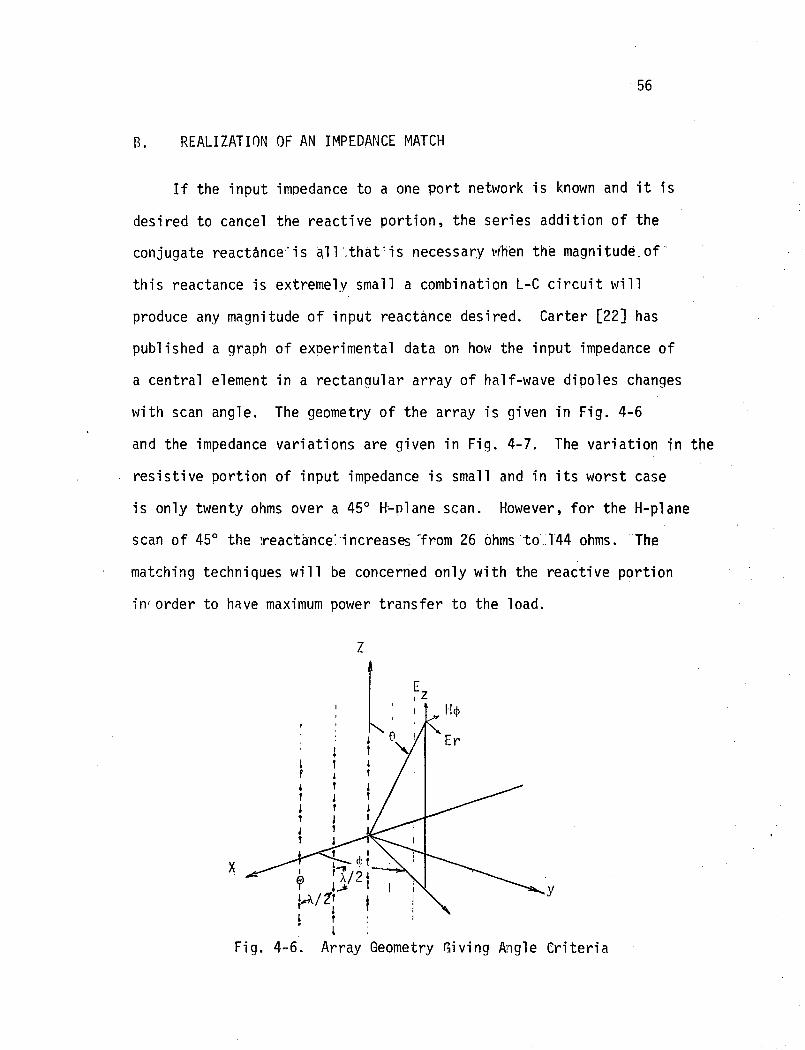
with scan angle. The geometry of the array is given in Fig. 4-6
and the impedance variations are given in Fig. 4-7. The variation in the
resistive portion of input impedance is small and in its worst case
is only twenty ohms over a 45 0H~plane scan. However, for the H-plane
scan of 45 0 the :reactimce:i ncreases-from 26 ohms 'to 144 ohms. The
matching techniques will be concerned only with the reactive portion
in' order to have maximum power transfer to the load.
y
~iving Angle Criteria
z
l,j E1Ij,jTj,j
I,ITJ,jTj
f II dJ r
k '1/2~-T !.J< I1,1.../'[f i, 1 I1 r• L
Fig. 4-6. Array Geometry
x

·180,.....----.---,..---,---.--,-----,57
6=90° Corresponrl~ :toH···Pl ane Scan
I
I
/
// 8=45°
I,/
/ .-/ .- 8=45.0
/ /'./ /'
./"
~ Resistance-- _ Reactance.
8--90'0/
/8;:60°-------
./' ./
./ / --- .....- ~.-- .- .----~ ..;..--0-
~.:=.oOJ(J
s::ttl\:lOJC:'·QOEJ
.......
o Scan fl,ng1 e a
Fig. 4-7. Variation of the Input Impedance of a Central Element of a
61 Element ~/2 Dipole Array Over a Ground Plane.
The spacing between the elements of the dipole array is a half
wavelength, therefore for H-plane scan (8=90°) the scan angle occurs
for a phas i ng between elements of o'x'
~x = kdx sin a + Ox (4-l0a)
The condition ~x=O points the beam in the z direction. Solving for
Ox gives
- 211" AOx = kdx sina = -- 2" sin a (4-17)
A
. -1 -0a = Sln (-2. ) (4-18)
11"

50'-'
2.0 153-j5.3153.1
After MatchInput Impedance
IZ. I1n153
1531533.1
0.0
Before t1atchScan angle Phase Input Impedance
ex (\ Z. IZ. I1n 1n
0° 0 153+j26 155.4
30° -90° 170+j75 185.8
45° -12]0 172+j143 223.6
Table 4-2. Data Necessary for Matching H-Plane Scan
Wh~n the input impedances for the scan angles are known as given in
Fig. 4-7 then the H~Dlane can be matched with the aid of a Smith Chart.
The following steps are illustrated in Fig. 4-8.
1. Choose the broadside impedance as a normalization factor
and convert it to pure resistance. This meant in-our
example a series addition of -j26.
2. Normalize all other impedances\.lJith the broadside impedance.
For our example Zn = 153:. all Zi n/ZO so we can enter the
chart.
3~ Convert all impedance points to admittance points.
4. Rotate the admittance locus to a curve of constant conduct-
ance this is accomplished by adding series t-lines.
Notice: the locus always rotates toward the generator.
5. The equivalent susceptance Beq. needed for r=O is seen
graphically to be -.8Z0 for our example. However, we have
shown in Eq. 4-15 that this can be solved by adding a shunt~
susceptance Of B = 3.1 = -.258 Zn

oc) Rotate Locus Clockwise to
Circle of Constant Conductanceby 4ddi ng a Lengt.h L of t··l i ne.
... ".
/'V\I\ '.\ .r'"\. \ " ,.",.-'/
od) !idd shunt of
Equivalent Susceptance
LI.i I( }
~.~._:-~::::<::,._,
.-" '"'l = .238),\
ntel~ Normal i zedmpeciance Locus
a.)
Fig. 4-8. Graphical Analysis of Imoedance Matching Technique.
In order to obtain the results given in the last column of Table
4-2 the circuit of Fig. 4-9 must be implemented.
y
1-:---,1----; j 39 f / _.
I--~-' ~/Mutual COUOl, ingBehind Ar:~ay
153 l
- -~
',-I'lutual CouplingAbove Array
Fig. 4-9. Equivalent Circuit for H-Plane Scan Impedance Matching of an
Array Characterized by Data Given in Fig. 4-7.
L = .238\
Antenna

60
C. REALIZATIONS USING MICROSTRIP-COMPONENTS
Once the equivalent values of admittance have been determined by the
methods of Section 4-2 the components can be fabricated using MIC techniques.
In the example just given a susceptive admittance of -39.5 ohms is
necessary. At a frequency of 2.5 GH z and if a single component is used,
this value corresponds to an extremely small inductance of 1.61
picohenrys or a 24 mil length of 50 nmicrostrip on 24 mil thick alumina.
Thi s value is impracti ca1. However , small "effecti ve" inductances and
capacitances can often be obtained using parallel or series L-C net
works composed of realizable LiS and C's. The common L-C tank circuit
is an example of this and is seen in Fig. 4-10 along with its properties.
In Fig. 4-11 the admittance versus frequency characteristics of a series
L-C network are illustrated.
[~utV t . . 1
B Capaciti veou w 0= ,!_'-
r;y wC'w + y.
~ln w
KI 1Yin=j (wc-~L) ~O
w/ -i:;t, inductive
Fig. 4-10. Properties of a Circuit with Parrallel Land C.
voutI _ 1w --o iCC·
By:;.,I Capaci ti veln I
+ .'CAl w
Fig. 4-11. Frequency Characteristics of a Series L-C Network

61
The equation for the innut admittance of the circuit of Fig. 4-10(a)
is
v. = j B = j (wC - -Ll
)1n w(4-19)
where B is the susceptance. Returning to the example, a value of
B = -39.5 is required. If Eq. (4-19) is solved for L given any C
and using the parallel L-C network, it will turn out that the value
of L is again too small to be practical. When a series L-C circuit
is used tne input admittance is
Vin = jB ::: j 11wC - wL
(4-20)
Choosing a value of. 1.0 nanohenry for L to achieve a value for
B = -39.5 the value of C is 4.07 picofarads. All of these values
are parctical and have been built in usable microwave integrated
circuits [18]. The capacitor with a value of 4.07 picofarads can be
constructed as a lumped element by the classical method of dielectric
separated metal sheets or the interdigital capacitor. Section 4-4
contains the theoretical work by Alley [14] on the interdigital
capacitor. Also curv~s are given which can be used to determine
the parameter values necessary to construct the capacitor. If the
antenna elements are modular a portion of the necessary capacitance
could be put into each module as depicted in Fig. 4-12

r; --\
50nMicrostrip
62Interdigital
~acitorrl ,--I-....,..-J
l~:'ln·I I 1
! IU
Inductance I~odul e
I I Ha 11 "'"
I Cor nectoII
nI
I,
Ii
Fig. 4-12. Interdiqital Capacitor for Use in Modular Antenna Elements
The value of the capacitance of each capacitor will be 8.14
picofarads. Using Eq. 4-21 and Fig. 4-]5 the necessary parameters
can be determined. The results are: X = 2 mil, N = 20, £ = 30.2 mil,
w = 158 mil, £r = 10. Refer to Fig. 4-13 for interpretation of these
values. However, nad the capacitor of Fig. 3.6 been used with Si02 as
the dielectric for a spacer 1 ~m thick,the value of 8.14 picofarads
would require a surface area of 389 mi1 2 whereas the IdC needs 4740
mi1 2. This area is obviously less than the interdigital capacitor.
The production of a metal sandwich capacitor requires more steps and
in thus costlier. The inductor values can be obtained from Eq.(3-1)
or Eq. (3-4) and are realized from the lengths of T-line connecting
the capacitor between elements. The parasitic capacitance of the
interdigital capacitor has a value of 2.14 x 10⁻¹⁴f and is not
considered.
D. THE INTERDIGITAL CAPACITOR
Microstrip Input==;I:~~ii!i~~Substrate-----~ ~
Ground Plane
Fig. 4-13. The Interdigital Capacitor on Dielectric of Thickness d
Above a Ground Plane.

63
The interdigital capacitor can be used as a lumped element
interconnecting circuit element if the capaeitive values required fall
in the range 0.1 to 10.0 picofarads.
R C
Fig. 4-14. Equivalent Circuit for the Interdigital Capacitor
The terminal strip capacitance Ct and the finger parasitic
capacitance are much less than the value of C. The important restric-
tion being that Cl and Ct can be neglected if the capacitor-frequency-3product falls below 2 x 10 . The value for the capacitance C has been
analyzea'-' by Alley [14] and his forml,lla for C is
where
(e: +1)C = ,r ~ [(N-3~ Al + A2] picofarads
W
w= width of terminal strips in inches£ = length of finger in inches€r = relative dielectric constant
(4-21)
. 13 .26
.12 2 .24 A2
Al
.11 .22
.10 .20 pf/inch
pf/inc;:h .09 .12
.08 . 16
:07 .11 d/x2
Fig. 4-15. Computati ona1 Graph for Determination of Al and A2 Given the
Dielectric Thickness d and Finger Separation X.

64
The prediction of the capacitive value from Eq. (4-21) is subject
to the restraint that the width of the fingers and the separ~tion of the
fingers is identical. The series resistance R forms a resonant circuit
with Cl and Ct whiGh can be treated as some total parasitic capacitance
and the effect of this filter circuit should be avoided. The series
resistance is a function of the sheet resistance and is given by:
1. 333 Q, RsR = XN (4-22) .
where Rs is the sheet resistance. For gold pl~t~drcoriduttors~four~kRin
d~pths thick the sheet resistance is 1.5 x 10⁻⁶~. The total parasitic
capacitance can be approximated using the surface area of the capacitor
and Eq. (3-6). With these values known the problem of the resonant
circuit can be avoided.
The quality factor of this capacitor is giv~n by:
o 0'c 'c
Q= Q +QC d
(4-23)
where Qc is the quality factor associated with the conductor and Qdis asso~iated with the dielectric.
and
Q = 0.75 NXc we Q, Rs
1 1Qd = tan e = dielectric loss tangent
(4-24)
(4-25)
The interdigital capacitor is acting as a lumped element even
though it is above a ground plane and thus it can be fed directly by
a distributed microstrip transmission line. Another attractive

65
characteristic is its trim capability,' providing that in the inital
fabrication additional fingers are produced. This along with
simultaneous one step production reduces costs.

CHAPTER V
POWER LIMITS AND WIDE-BAND BALUN FEEDING OF A SPIRAL ANTENNA
For a planar array which is designed for wide scan angles the
ideal array element would have a nearly hemispherically isotropic
pattern and operate well in an array environment. Many airborn and
spacecraft systems utilize circular polarization so antenna alignment
between transmitter and receiver is not critical. If an array is to
handle a large number of channels or have a multimode, multispectral
capacity, the element should also have constant characteristics over
a large bandwidth. All these features are obtained with the spiral
antenna which has a comparatively large beam width with a polarization,
axial ratio close to one. Frequency bandwidths of approximately 2:1
are common for spiral antennas. Bawer and Wolfe [24J have published
experimental data for a typical spiral antenna, the results of which
are summarized in Fig. (5-1). From Fig. (5-1) it is clear the spiral
antenna is only approximately frequency independent, however, it should
be adequate for most wide band applications.
A spiral antenna which is compatable with MIC technology is amenable
to flush mounting in the array surface,and its mass is small compared
to other antennas which generate circular polarization. In order for
the spiral to radiate in a well behaved fashion a high turn density is
recommended. However, power considerations set a limit since they require
enough spacing between arms to avoid voltage breakdown. Therefore, a
66

67
tradoff must be determined between the number of turns'made by a spiral
arm and maximum power radiation desired. When complementary symmetry
use9, the spacing between arms equals the width of the conductor
forming the arm. Usually the spiral arms are terminated in some form
of dissipating load to avoid the generation of spurious modes due to
reflection. Continuous power per element should not exceed nine watts
for an 18 GH z spiral etched from gold clad alumina and designed with
six turns and 2:1 bandwidth.
1.33 f 0
>,_.+>.Q .....
"Ou(/) "'-""" .,....
..... +>xoo.
c::x:: e";" -rI +> r
C ro~·CS-W
4 r--;r--~-r--r---,----r-.,.---,r--o-""--""--""T
32
1
O'-.&.-...J--L..--L_L...-~...J--L..---:'--...J---I
.66 fa
2.01 I:;"V
1.0
~66 fa
.I:::. 80+>aro0'",..... 70~~Q) rtl 60
"> Q)c::r:co
.66 fa fO 1. 33 fa
Fig. 5-1. Characterestics of an Archimedian Spiral Antenna Designed
with a Center Frequency of fa.

68
Two alternatives of feeding a wideband spiral in the normal mode
(i.e. current 1800 out of phase at the feed) from an unbalanced
transmission line are investigated. The Bawer balun has its worst
impedance match in the operating band at the center frequency. It
also requires two sides of etched microstrip for realization. The
Craven balun in also matched at the extremes of its operating band,
but it is matched at the center frequency also. Spiral antennas when
put in an array environment normally are placed one quarter wavelength
above a ground plane to eliminate back radiation and provide shielding.
The construction of the Craven balun is such that its ground. plane can
serve the above purposes as well as its transformer function. Its
feed lines run directly from the MIC network to the center balanced
feed of the spiral, and this balun is thought best suited for X-band
and above spiral feeds.
A. POWER LIMITS
The maximum power handling capability of the spiral antenna will
be a function of the RF voltage breakdown between the conductors and
the maximum allowed current flow through the conductors. Once the
input impedance is known the maximum power the antenna element can
radiate will be determined by which occurs first, voltage breakdown
o~ excessive current causinq subsequent failure due to overheating.
In the case of a dc voltage between two parallel plates in dry
air at standard pressure the electric field intensity necessary for
breakdown is 30,OOO·.volts/cm_[29].When a'~jgh 'frE/quencY'volti:ige>is
impressed between the conductors the electric field producing

69
breakdown is less. How much less depends on the field configuration
resulting from the applied RF voltage. In the case of conductors
interfaced by air on one side and a dielectric on the other, the
electric field will be altered thus increasing the electric field
in the air. The breakdown voltages versus conductor spacing with
frequency as a parameter are empirically given in Fig. 5-2 for
two plates in dry air at one atmosphere pressure (14.7 psi or 760
mm Hg).1600 ...-----.-_-..-_...,.-_....-----._--,-_.....------.
50 HZ
400
III
~ Eo
'"0 800.::L-eoOJ~
co
OJO'l
~ 1200,.....o>
.Gap Width (mm)
Fig. 5-2. Variation of Breakdown Voltage vs. Conductor Spacing as a
Function of Frequency [15J.
If the spiral antenna is designed to operate at a center frequency,
fb, of 18 GH z ' the free space wavelength is 1.669 cm. Using the band
theory approximation for spiral [24J, most of the radiation occurs at
a circumference of one wavelength which at 18 GHz gives
C = TID = 1.668 cm, (5-1 )
Available data on the spiral antenna has shown that the supporting
dielectric substate has little effect in reducing the electrical size of

70
the antenna and phase velocity of the two wire balanced transmission line
that forms the antenna. Thus the wavelength of the RF energy is not
significantly different from that of free space. Therefore, the
diameter of a spiral with a 2:1 bandwidth and fO = 18 GHz is 0.795 cm.
Let us consider an Archimedian spiral illustrated in Fig. 5-3. Its
defining equation is given by
r = A8 + S (5-2)
r = radius from a point on an arm to center
A = growth constant
S = orgin constant. ,
polar angle in radians8 =
vi = w'j dth ofconductor
S = ConductorSpacing
Fig. 5-3. 1.5 Turn Archimedian Spiral Antenna
The input impedance to a complementary antenna has been shown to
be 189 ohms [25J. In order for the spiral antenna to approximate a
complementary antenna the conductor width should equal to the spacing.
Applying this condition, Eq. (5-2) becomes:
r = s [~ + 1J1T
(5-3)

71
The value of the conductor spacing S will be a design criteria
determined by the number of spiral arm turns N. Thus the spacing
S in terms of the spiral diameter becomes:
oS = -=8NC:--+---=2 (5-4)
For the case of a six turn, 18 GH z spiral the spacing S is 0.159 mm.
Assuming the breakdown in air occurs for a field strength of 30 kv
per cm. and using a safety factor of 2.4, a maximum of approximately
200 volts is possible between conductors. This corresponds to a
maximum possible current flow' which is on the order of one ampere
since the input impedance is approximately 189 ohm?~ It is also
necessary to theoretically determine the maximum current density
which can be tolerated by the metal spiral arms. The following
parameters must be considered:
1. Conductor resistivity p
2. Conductor cross-sectional area
3. Thermal properties of adjacent media
4. Conductor melting point
5. Joule heating of conductor
6. Specific heat of conductor and media
7. Operating frequency (skin effect)
To avoid the problem of theoretically evaluating the above for
the maximum current carrying capacity I , an approximate I canmax maxbe found by considering the current limitations of specific conductors
given their cross sectional area.

5 72ro
4(lJS-
c::e,.....
3r.:.< "JC E0 L;.,..-~ \.0
2I"; I(lJ 0
U')
Vl1VI
0S-
Ou
Current (amps r~s)
Fig. 5-4. Maximum Current Capability of Copper Wire (Cu melting point 1080°C)
For a microstrip spiral the conductor thickness is usually 3.8-5.0
micrometers or about ten skin depths at 18 GH z' However, the current-5will see an effective conductor thickness of 4.1 x 10 cm due to the
skin effect. The metalization is a combination of silver and gold which
melts round 1000°C and will support a maximum current density of
5 x 10⁵ amps/cm2. The conductor width is 1.59 x 10⁻² cm. and thus-7 2has a cross sectional area of 6.5 x 10 cm. This leads to a'f'9ure.of
325 rna. for Imax ' After applying a safety factor of two an 18 GH zcomplementary microstrip spiral antenna mounted on alumina can radiate
8.5 watts of continuous rms power per element which is much less than
the maximum power limit set by considering voltage breakdown in air.
The evaluation of peak pulse power in terms of breakdwon voltage alone
is-allowable provided the duty cycle is small enough to restrict critical
ion accumulation. Note that spacecraft applications present an entirely
new problem where material outgassing at low pressures may produce
breakdown at considerably lower values then in air. Using a breakdown
voltage safety factor of 100 would give a power limit of about 4 watts
per element which is a confortab~e margin compared to the low powers
produced by the sources that might be used at this frequency.

73
B. BALUN FEEDING OF THE SPIRAL ANTENNA
A balun is a transformer which performs matching between balanced
and unbalanced transmission lines. In spiral MIC applications the balun
is an interface between the balanced spiral feed and the unbalanced
microstrip t-line. The microstrip circuitry is usually designed using
the maximum quality factor 50 ohm t-line whereas the spiral input
impedance for complementary symmetry is around 189 ohms. It is
desirable to have the magnitude of the spiral's impedance closer
to the microstrip impedance to avoid large power reflection. It
is speculated that increasing the conductor width-to-spacing ratio
to greater than unity decreases the dual-arm spiral antenna's input
impedance. Because the spiral is used inwidebiH'H1"" applications the
balun should also be widebanrl~. Consider the input impedance of the
transmission line network of Fig. 5-5 [27J. The input is a coaxial
t-line and the output is a twin line utilizing the shielding of the
two coaxial lines. The theory is developed in terms of balanced
and unbalanced lines such that a substitution of microstrip t-line
parameters is obvious.
ZlAC
__~B
l7'-Be
B
out
Fig. 5-5. Wide Band Balun

74
Using nodal analysis we can express the impedance ZAC as:
(5-5)
implying:
(5-6)
The input impedance to an open circuit t-line with characteristic
impedance Zi is:u
(5-7)
For a short circuited t-line of impedance Zb the input impedance is:
(5-8)
Substituting Eq. 5-7 and Eq. 5-8 into Eq. 5-6 we get:
where
RL = Real part of the load impedance
XL = Imaginary part of the load impedance'
Zb = Characteristic impedance of the balanced T-line
Zu = Characteristic impeqamce of the unbalanced d T-line
61 = Electrical length of twin line to short in radians
62 = Electrical length of coaxial line to open in radians
In order to draw conclusions from Eq. 5-9 the following pedagogical
approximations are made: X2 = 0, 61 = 62 = 6, and Zu = Zb. The result

75
is Zin = ZAC 0.e. a perfect impedance match at the frequencies corresponding
to 6 which solve the equation sin 26 = Zin/RJ, For 6 = 90° the length
of t-line (2) is one quarter wavelength at fa and thus at the frequency
fOJZ AC = ZL' Obviously, the center frequency, fO' has the highest
reflection of power of all frequencies in the operating band,and in the
case where Zi n = 50n and RL = 189n an auxi 11 ary impedance transformer
is needed. A tappered line will suffice. To increase the bandwidth
of the balun the condition Zu = R2L/Zb should replace Zu ~ Zb' A
comparison of these two choices is illustrated in Fig. 5-6.
5.0
4.0
3.0
2.0i
,;
8 degl'ees
Fig. 5-6. Graphical Interpretation of Eq. 5-9 with XL = 0 and 61 = 62 = 6;
Frequencies f l and f2 Correspond to Solutions of sin26 = Zin/RL
The spiral antenna is usually mounted over a cativity which is a
quarter-wavelength deep at the center frequency. This places a dimensional
restriction on the balun which is mounted perpendicular to the spiral
surface. Bawer and Wolfe [16] applied Robert's technique to microstrip
transmission line. The microstrip balun is illustrated in Fig. 5-7.

76
--, D/---..- - ,,' --.,I I
I • . - .~utPl1t
T.I.e .1 e
-HU H 1tappered
1ine --..,...:;>>-1
6 = A/4
~Input
a) Ground olane and balanced output b) unbalanced microstr1n iYiDllt
Fig. 5-7. Bawer and Wolfe Printed Circuit Balun.
The necessary parameter values for constructing the desired micro
strip input impedance and taper (impedance transformer) are given in
Chapter II. The impedances can be calculated using Eq. 2-57. The
characteristic impedance for the balanced transmission line has been
empirically determined [16] and is listed in Fig. ~-8.
HIS 'Zo (ohms)
2 220
4 185
6 170
8 160
10 155
Fig. 5-8. Characteristic Imoedance for a Two Ribbon Balanced Line

77
The most undersireable characteristic of the Bawer balun concerns
the large impedance mismatch resulting about its design center frequency.
On the other hand, the microstrip meander line phase shifter when used
with the broad-band phase shifting properties of coupled microstrip
results in a balun technique with a relatively frequency independent
impedance characteristic. Negligible VSI~R at the center frequency;
and normal mode excitation are achieved using this method. Craven
[17J using the method of Schiffman [28J ~tilized this method of balun
design,but Craven's balun unnecessarily occupys a large area. A more
optimum balun design using microstrip t-lines is illustrated in Fig. 5-9.
The broad-band 90 0 phase shifters have less than a four degree phase
deviation over a 2:1 bandwidth. Figure (5-10) is a Shiffman type-A
network. The phase shift ~ 'of coupled microstrip is given by
-1Zoe
tan2 eZoo
-~ = cos
Zoe + ta1l2 e (5-10)L
00
where
Zoe = characteristic impedance of one line to ground when
equal in phase currents flow in both lines
Zoo - characteristic impedance of one 1i ne to ground when
equal out-of-phase currents flow in both lines
e = 8£ = electrical length of a uniform line length £
and phase constant 8.

I~ .9. ..Iv. -r--t:========::J: 11n '-,- 7COUP od Microstrip
78
vout r!reande\~ Line ofLength 69.,
Fig. 5-9. Coupled Microstrip Balun.
~.9-
v,.. 1350 T '\veHl
~cf> = cf>2 - <1>1300 3 Q,
240 1l/lQ)Q)
180~C')Q)Cl
120-e-
60
e Degrees
Fig. 5-10. 90° Broad-Band Phase Shifter
The input impedance Zc~ to the coupled microstrip line is given by
(5-11 )
and the input impedance at the output port is independent of frequency and
is the series sum of the impedance of the uncoupled microstrip Zo and Zcm'
The use of Fig. 2-2 will aid in the design of the coupled microstrip. The
input impedance to the balun will be the par~1'~1~ sum of the impedances Zo and
Zcm'

79
REFERENCES
[lJ Wheeler, H. A., "Transmission-Line Properties of Parallel StripsSeparated by a Dielectric Sheet," IEEE Trans. on Microwave Theoryand Techniques, Vol. MTT-13, March 1965, pp. 172-185.
[2]' Assadourian, F. and Rimai, E., "Simplified Theory of r1icrostripTransmi ssi on Systems, II Proceedi ngs of the I. R. E., December 1952,pp. 1651 -1657.
[3J Judd, S. V., et al. IIAn Analytical Method for Calculating Microstrip Transmission Line Parameters," IEEE Trans. on r1icrowaveTheory and Technigues, Vol. MTT-18, No.2, Febuary 1970, pp. 78-87.
[4J Cohn, S. B., "Shielded Coupled-Strip Transmission Line,1I IRE Trans.on Microwave Theory and Techniques, October 1955, pp. 29-38.
[5J Hilberg, IIFrom Approximations to Exact Relations' for CharacteristicJmpedances. II I EEE Trans. on Mi crowave Theory and Techni gues , Vol.MITT~lZ, May 1969, pp. 259-265.
[6J Bates, R. H. T., liThe Characteristic Impedance of the Shielded SlabLine," IRE Trans. on Microwave Theory and Techniques, January 1956,pp. 28-33.·
[7J Hyltin, T. M., "Microstrip Transmission on Semiconductor Dielectrics,"IEEE Trans. on Microwave Theory and Techniques, Vol. MTT-13,November 1965, pp. 777-781.
[8J Green, H. E., liThe Numerical Solution of Some ImpoY'tant TransmissionLine Problems, II l.~.EE Trans. on. Mi crowave Theory and. Techni ques,Vol. MTT-13, September - 1965, pp. 676-692. .
[9J Yamashita, E. and Mittra, R., IIVariational Method for the Analysisof Microstrip Lines," IEEE Trans. on Microwave Theory and Techniques,Vol. MTT-16, April 1968, pp. 251-256.
[10J Terman, F. E., Radi 0 Engi neer I s Handbook. New York: McGraw-Hi 11 ,1943.
[llJ Caulton, M. and Sobol, H., "Microwave Integrated-Circuit Technologya Survey", IEEE Journal of Solid-State Circuits, Vol. SC-5, No.6,December 1970, pp. 292-302.

80
[12J Lehrfeld, S. S., "\,}hat if You Don't Use Alumina?" Microwave,March 1971, pp. 54-56.
[13J Hannan, P. H., et al., "Impedance Matching a Phased-ArrayAntenna Over Hide Scan Anqles by Connecting Circuits," IEEETrans. on Antennas and Propagation, January 1965, pp. 28-34.
[14J Alley, G. D., "Interdigital Capacitors and Their Applicationto Lumped-Element Microwave Integrated Circuits", IEEE Trans.on Microwave Theory and Techniques, December 1970, pp. 1028-1033.
[15J Meek, J. M., and Cragge, J. D., Electrical Breakdown of Gases,Oxford University Press, London, 1953, pp. 381.
[16J Bawer, R. and Holfe, J. J., II A' Printed Circuit Balun for Use withSpiral Antenna's," IRE Trans. on Microwave Theory and Techniques,May, 1960, pp. 319-325.
[17] Craven, J. H., "A Novel Broad-Band Balun", IRE Trans. on MicrowaveTheory and Techniques, November 1960, pp. 672-673.
[18J Sobol, H., "Application of Integrated Circuit Technology toMicrowave Frequencies," Proc. IEEE, Vol. 59, August 1971, pp.1200-1211 .
[19J M. Caulton, B. Hershenov, S. Knight, and R. DeBrecht, "Statusof Lumped Elements in Microwave Integrated Circuits-Present andPuture," IEEE T-MTT, Vol. MTT-19, July 1971, pp. 588-599.
[20J S. B. Cohn, "S1 ot-Line an Alternative Transmission Medium forIntegrated Circuits," IEEE G-MTT Int. Microwave Symp. Digest,May 1968, pp. 104-109.
[21] C. P. Hen, "Coplanar Haveguide, a Surface Strip Transmission LineSuitable for Nonreciprocal Gyromagnetic Twill Applications,"IEEE G-MTT Int. Microwave Sump. Digest., May 1969, pp. 110-114.
[22J Carter, P. S., Jr., "Mutual Impedance Effects in Large BeamScanning Arrays', IRE Trans. on Antennas and Propagation, May 1960,pp. 276-285. ..
[23J Dudgeon, J. E., II Effiei ency and Effi ci ency Improvement ThroughCompensation," Technical Report No.1, NAS8-25894, October 1970.
[24J Bawer, R. and Wolfe, J. J., liThe Spiral Antenna", IRE ConventionRecord, 1960, pp. 87.

81
[25J Rumesy, V. H., Freguency Independent Antennas, Academic Press,New York, 1966, pp. 27.
[26J Bolz and Tuve, Handbook of Tables for Applied Engineering Science,CRC, 1970.
[27] Roberts, \'1. K., "A New \~ide-Band Balun, II Proceedings of the IRE,December, 1957, pp. 1628-1631.
[28J Schiffman, B. M., "A New Class of Broad-Band Microwave 90-DegreePhase Shifters," IRE Trans. on Microwave Theory and Technigues,April, 1968, pp. 232-237.
[29J Southworth, G. C., Principles and Applications of Waveguide Transmission, D. Van Nostrand, New York, 1950.