microstructure stability of silver electrodeposits at room temperature
TRANSCRIPT
Available online at www.sciencedirect.com
Scripta Materialia 58 (2008) 96–98
www.elsevier.com/locate/scriptamat
Microstructure stability of silver electrodeposits atroom temperature
Karsten Hansen and Karen Pantleon*
Technical University of Denmark, Department of Manufacturing Engineering and Management, Kemitorvet b. 204,
DK-2800 Kgs. Lyngby, Denmark
Received 13 July 2007; revised 10 September 2007; accepted 24 September 2007Available online 22 October 2007
In situ quantitative X-ray diffraction analysis was used to investigate the kinetics of microstructure evolution at room temper-ature (self-annealing) in an electrodeposited silver layer. As a function of time at room temperature the as-deposited nanocrystallinemicrostructure evolved considerably: orientation-dependent grain growth and changes of the preferred grain orientation occurred. Itis demonstrated for the first time that self-annealing occurs for electrodeposited silver layers and, hence, is not a unique feature ofcopper as often suggested.� 2007 Acta Materialia Inc. Published by Elsevier Ltd. All rights reserved.
Keywords: Self-annealing; Electroplating; Texture; Grain growth; Silver
Silver is increasingly attracting attention as a poten-tial interconnect material [1,2] and the replacement ofcopper by silver in the future is being discussed in similarterms to those previously used for the changeover fromaluminum-based materials to copper. Indeed, the lowerelectrical resistivity of bulk silver compared to bulk cop-per is promising; however, the properties finally dependon the microstructure of the films. For electrodepositedcopper it is well known that the as-deposited microstruc-ture is not stable, but evolves as a function of time atroom temperature (self-annealing) (e.g. [3–6]), andchanges may continue at elevated temperatures [7,8].The microstructural evolution during self-annealing ofcopper electrodeposits is accompanied by considerableimprovements in the electrical conductivity and electro-migration resistance, and is hence of importance for thefunctionality of copper interconnects.
For silver electrodeposits, the thermal stability of themicrostructure and associated properties has been inves-tigated at elevated temperatures [9,10], but to the knowl-edge of the authors, self-annealing of silver layers atroom temperature has not been reported previously.So far, evolution of the microstructure at room temper-ature has only been observed in bulk nanocrystalline
1359-6462/$ - see front matter � 2007 Acta Materialia Inc. Published by Edoi:10.1016/j.scriptamat.2007.09.033
* Corresponding author. Tel.: +45 4525 2207; fax: +45 4593 6213;e-mail: [email protected]
materials during mechanical loading [11–14] or in thincopper films [3–6,15].
Silver was electrodeposited from a commercial cya-nide electrolyte (Engbright) containing 45 g l�1 AgCN,165 g l�1 KCN, 15 g l�1 K2CO3 and appropriate addi-tive concentrations (Engbright S101 and S201). Thebath temperature was 21 �C. A 4 lm thick silver layerwas deposited with a current density of 2.75 A dm�2
on a copper sheet.For investigating the kinetics of self-annealing in situ
X-ray diffraction (XRD) analysis was started immedi-ately after the silver layer was deposited, cleaned, driedand mounted in the X-ray diffractometer (Discover D8,Bruker AXS), i.e. within about 15 min after deposition.CuKa radiation was used to measure the diffractionlines corresponding to (111), (200) and (222) latticeplanes. Line profiles were fitted by applying pseudo-Voigt functions and microstructure information in termsof grain size and microstrain was obtained by applyingboth the single-line method [16] and the Williamson–Hall method [17] after correction for instrumental linebroadening. In addition to repeated measurements ofvarious diffraction lines, quantitative crystallographictexture analysis was also performed in turn with the linescans. For texture analysis, 111 and 220 pole figureswere recorded (measurements were restricted to quartersof the pole figures, which are representative due to thepresence of fibre textures) and the orientation distribu-tion function was calculated. Scans of the various
lsevier Ltd. All rights reserved.
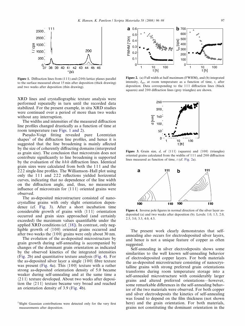
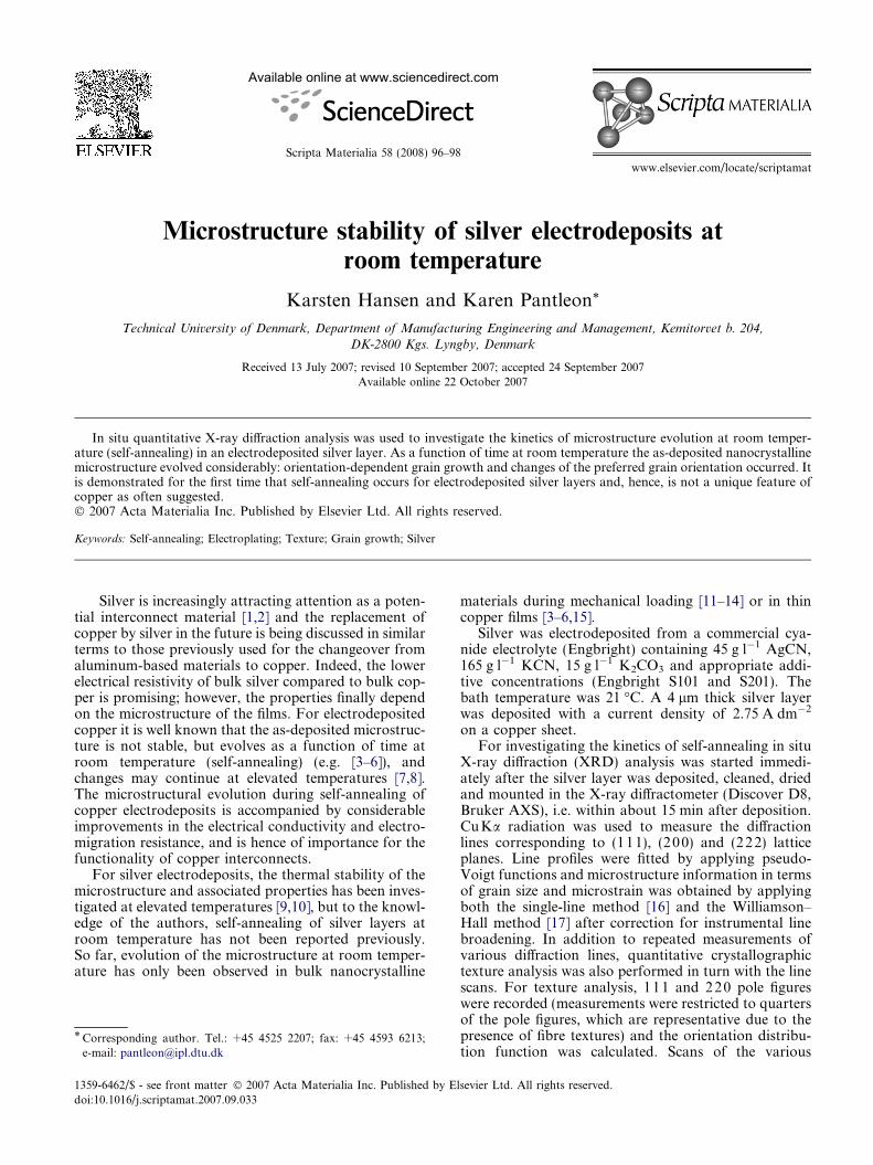
Figure 1. Diffraction lines from (111) and (200) lattice planes parallelto the surface measured about 15 min after deposition (thick drawing)and two weeks after deposition (thin drawing).
Figure 2. (a) Full width at half maximum (FWHM), and (b) integratedintensity, Iint, at room temperature as a function of time, t, afterdeposition. Data corresponding to the 111 diffraction lines (blacksquares) and 200 diffraction lines (grey triangles) are shown.
Figure 3. Grain size, d, of h111i (squares) and h100i (triangles)oriented grains calculated from the widths of 111 and 200 diffractionlines measured as function of time, t (cf. Fig. 2a).
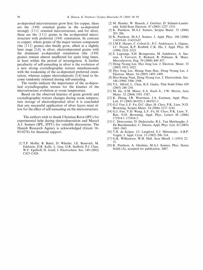
Figure 4. Inverse pole figures in normal direction of the silver layer as-deposited (a) and two weeks after deposition (b). Levels: 1.0, 1.5, 2.0,2.5, 3.0, 3.5, 4.0, 4.5.
K. Hansen, K. Pantleon / Scripta Materialia 58 (2008) 96–98 97
XRD lines and crystallographic texture analysis wereperformed repeatedly in turn until the recorded datastabilized. For the present example, in situ XRD studieswere continued over a period of more than two weekswithout any interruption.
The widths and intensities of the measured diffractionline profiles changed drastically as a function of time atroom temperature (see Figs. 1 and 2).
Pseudo-Voigt fitting revealed pure Lorentzianshapes1 of the diffraction line profiles, and hence it issuggested that the line broadening is mainly affectedby the size of coherently diffracting domains (interpretedas grain size). The conclusion that microstrain does notcontribute significantly to line broadening is supportedby the evaluation of the hhh diffraction lines. Identicalgrain sizes were calculated from both the 1 11 and the222 single-line profiles. The Williamson–Hall plot usingonly the 11 1 and 222 reflections yielded horizontalcurves, indicating that no dependence of the line widthon the diffraction angle, and, thus, no measurableinfluence of microstrain for h111i oriented grains wereobserved.
The as-deposited microstructure consisted of nano-crystalline grains with only slight orientation depen-dence (cf. Fig. 3). After a short incubation timeconsiderable growth of grains with h111i orientationoccurred and grain sizes approached (and certainlyexceeded) the maximum values quantifiable under theapplied XRD conditions (cf. [18]). In contrast, only neg-ligible growth of h10 0i oriented grains occurred andafter two weeks the h1 00i grains were only about 30 nm.
The evolution of the as-deposited microstructure bygrain growth during self-annealing is accompanied bychanges of the dominant grain orientation as indicatedby the observed kinetics of the integrated intensities(Fig. 2b) and quantitative texture analysis (Fig. 4). Forthe as-deposited silver layer a single h100i fibre texturewas present (Fig. 4a). This h100i texture with a ratherstrong as-deposited orientation density of 5.0 becameweaker during self-annealing and at the same time ah211i texture developed. About two weeks after deposi-tion the h2 11i texture became very broad and reachedan orientation density of 3.9 (Fig. 4b).
1 Slight Gaussian contributions were detected only for the very firstmeasurements after deposition.
The present work clearly demonstrates that self-annealing also occurs for electrodeposited silver layers,and hence is not a unique feature of copper as oftensuggested.
Self-annealing in silver electrodeposits shows somesimilarities to the well known self-annealing behaviorof electrodeposited copper layers. For both materialsthe as-deposited microstructure consisting of nanocrys-talline grains with strong preferred grain orientationstransforms during room temperature storage into aself-annealed microstructure with considerably largergrains and altered preferred orientations—however,some remarkable differences in the self-annealing behav-ior of the two materials were observed. For both copperand silver electrodeposits the kinetics of self-annealingwas found to depend on the film thickness (not shownhere) and the grain orientation. For both materials,grains not constituting the dominant orientation in the
98 K. Hansen, K. Pantleon / Scripta Materialia 58 (2008) 96–98
as-deposited microstructure grow first: for copper, theseare the h100i oriented grains in the as-depositedstrongly h111i oriented microstructure, and for silver,these are the h111i grains in the as-deposited micro-structure with preferred h1 00i orientation. In contrastto copper, where grains of the major texture component(the h111i grains) also finally grow, albeit at a slightlylater stage [3,4], in silver, electrodeposited grains withthe dominant as-deposited orientation (the h1 00igrains) remain almost unaffected for quite long times,at least within the period of investigation. A furtherpeculiarity of self-annealing in silver is the evolution ofa new strong crystallographic texture simultaneouslywith the weakening of the as-deposited preferred orien-tation, whereas copper electrodeposits [3,4] tend to be-come randomly oriented during self-annealing.
The results indicate the importance of the as-depos-ited crystallographic texture for the kinetics of themicrostructure evolution at room temperature.
Based on the observed kinetics of grain growth andcrystallographic texture changes during room tempera-ture storage of electrodeposited silver it is concludedthat any successful application of silver layers must al-low for the effect of self-annealing on the microstructure.
The authors wish to thank Christian Ravn (IPU) forexperimental help during electrodeposition and MarcelA.J. Somers (IPL, DTU) for valuable discussions. TheDanish Research Agency is acknowledged (Grant 16-03-0276) for financial support.
[1] T.P. Moffat, B. Baker, D. Wheeler, J.E. Bonevich, M.Edelstein, D.R. Kelly, L. Gan, G.R. Stafford, P.J. Chen,W.F. Egelhoff, D. Josell, J. Electrochem. Soc. 149 (2002)C423–C428.
[2] M. Hauder, W. Hansch, J. Gstotter, D. Schmitt-Landsi-edel, Solid-State Electron. 47 (2003) 1227–1231.
[3] K. Pantleon, M.A.J. Somers, Scripta Mater. 55 (2006)283–286.
[4] K. Pantleon, M.A.J. Somers, J. Appl. Phys. 100 (2006)114319-01–114319-07.
[5] J.M.E. Harper, C. Cabral Jr., P.C. Andricacos, L. Gignac,I.C. Noyen, K.P. Rodbell, C.K. Hu, J. Appl. Phys. 86(1999) 2516–2525.
[6] S. Lagrange, S.H. Brongersma, M. Judelewicz, A. Sae-rens, I. Vervoort, E. Richard, R. Palmans, K. Maex,Microelectron. Eng. 50 (2000) 449–457.
[7] Dong Nyung Lee, Hyo Jong Lee, J. Electron. Mater. 32(2003) 1012–1022.
[8] Hyo Jong Lee, Heung Nam Han, Dong Nyung Lee, J.Electron. Mater. 34 (2005) 1493–1499.
[9] Hyo-Seung Nam, Dong Nyung Lee, J. Electrochem. Soc.146 (1999) 3300–3308.
[10] T.L. Alford, L. Chen, K.S. Gadre, Thin Solid Films 429(2003) 248–254.
[11] M. Jin, A.M. Minor, E.A. Stach Jr., J.W. Morris, ActaMater. 52 (2004) 5381–5387.
[12] K. Zhang, J.R. Weertman, J.A. Eastman, Appl. Phys.Lett. 87 (2005) 061921-1–061921-3.
[13] G.J. Fan, L.F. Fu, D.C. Qiao, H. Choo, P.K. Liaw, N.D.Browning, Scripta Mater. 54 (2006) 2137–2141.
[14] G.J. Fan, Y.D. Wang, L.F. Fu, H. Choo, P.K. Liaw, Y.Ren, N.D. Browning, Appl. Phys. Letters 88 (2006)171914-1–171914-3.
[15] C. Detavernier, D. Deduytsche, R.L. Van Meirhaeghe, J.De Baerdemaeker, C. Dauwe, Appl. Phys. Lett. 82 (2003)1863–1865.
[16] T.H. de Keijser, J.I. Langford, E.J. Mittemeijer, A.B.P.Vogels, J. Appl. Cryst. 15 (1982) 308–314.
[17] G.K. Williamson, W.H. Hall, Acta Metall. 1 (1953) 22–31.
[18] K. Pantleon, A. Gholinia, M.A.J. Somers, Phys. StatusSolidi (A), accepted for publication, 2007.