mimicking synaptic plasticity and neural network using … · 2018-02-13 · mimicking synaptic...
TRANSCRIPT
CommuniCation
1706717 (1 of 8) © 2018 WILEY-VCH Verlag GmbH & Co. KGaA, Weinheim
www.advmat.de
Mimicking Synaptic Plasticity and Neural Network Using Memtranstors
Jian-Xin Shen, Da-Shan Shang,* Yi-Sheng Chai, Shou-Guo Wang, Bao-Gen Shen, and Young Sun*
J.-X. Shen, Dr. D.-S. Shang, Dr. Y.-S. Chai, Prof. B.-G. Shen, Prof. Y. SunBeijing National Laboratory for Condensed Matter PhysicsInstitute of PhysicsChinese Academy of SciencesBeijing 100190, P. R. ChinaE-mail: [email protected]; [email protected]. Shen, Prof. Y. SunSchool of Physical ScienceUniversity of Chinese Academy of SciencesBeijing 100190, ChinaProf. S.-G. WangInstitute of Advanced MaterialsBeijing Normal UniversityBeijing 100875, China
The ORCID identification number(s) for the author(s) of this article can be found under https://doi.org/10.1002/adma.201706717.
DOI: 10.1002/adma.201706717
≈1015 in the human brain. The intercon-nected neurons can store and process information simultaneously, and their operation is collective and adaptive.[3] The special architecture is completely different from the well-established von Neumann one, and can perform massive parallel computing.[2] To reproduce similar prop-erties by electronic circuits, many studies have been conducted to develop neuro-morphic computing systems, including those based on software programming and/or based on complementary metal oxide semiconductor devices.[4–7] However, some serious challenges exist, such as the energy consumption, complexity of the electric circuit, and the physical size of the computational systems, because com-plicated algorithms and/or circuits are required just for the functions performed by single neuron or synapse. Therefore,
to mimic effectively the brain operation mode, some nontradi-tional electronic elements will be required to realize the brain-like information storage and computing.
Memristive devices, i.e., devices that can keep track of the past resistance state through which the element has experienced,[8,9] have been widely studied to implement artificial synaptic devices in recent years, because the gradual resistance change of mem-ristive devices driven by external electric signals could be used to reproduce the plasticity of synapses, which is defined as synaptic weight, to represent the strength of the correlation between two neighboring neurons.[10–25] Practical implementa-tions of synaptic functions have been realized in various mem-ristive devices with different physical mechanisms, such as phase change,[10–12] ferroelectric domains,[13,14] magnetoresist-ance,[15–17] and redox-based resistive switching.[18–26] In addition to the memristive devices, other candidates and new principles toward artificial synaptic devices are worthy of study.
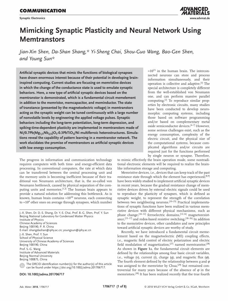
Recently, we have introduced a fundamental circuit meme-lement based on the magnetoelectric (ME) coupling effects, i.e., magnetic field control of electric polarization and electric field modulation of magnetization,[27] named memtranstor.[28] As shown in Figure 1a, the fundamental circuit elements are defined by the relationships among four basic circuit variables, i.e., voltage (v), current (i), charge (q), and magnetic flux (ϕ). The fourth element defined by the relationship between q and ϕ was assigned to the memristor by Chua,[29] but remained con-troversial for many years because of the absence of ϕ in the memristors.[30] It has been realized recently that the true fourth
Artificial synaptic devices that mimic the functions of biological synapses have drawn enormous interest because of their potential in developing brain-inspired computing. Current studies are focusing on memristive devices in which the change of the conductance state is used to emulate synaptic behaviors. Here, a new type of artificial synaptic devices based on the memtranstor is demonstrated, which is a fundamental circuit memelement in addition to the memristor, memcapacitor, and meminductor. The state of transtance (presented by the magnetoelectric voltage) in memtranstors acting as the synaptic weight can be tuned continuously with a large number of nonvolatile levels by engineering the applied voltage pulses. Synaptic behaviors including the long-term potentiation, long-term depression, and spiking-time-dependent plasticity are implemented in memtranstors made of Ni/0.7Pb(Mg1/3Nb2/3)O3-0.3PbTiO3/Ni multiferroic heterostructures. Simula-tions reveal the capability of pattern learning in a memtranstor network. The work elucidates the promise of memtranstors as artificial synaptic devices with low energy consumption.
Synaptic Electronics
The progress in information and communication technology requires computers with both time- and energy-efficient data processing. In conventional computers, the rate at which data can be transferred between the central processing unit and the memory units is becoming inefficient because of their tra-ditional von Neumann architecture, that is, the so-called von Neumann bottleneck, caused by physical separation of the com-puting units and memories.[1,2] The human brain appears to provide a natural solution for addressing this bottleneck. As is known, human brain contains ≈1010 neurons, each connecting to ≈104 other ones on average through synapses, which number
Adv. Mater. 2018, 1706717
© 2018 WILEY-VCH Verlag GmbH & Co. KGaA, Weinheim1706717 (2 of 8)
www.advmat.dewww.advancedsciencenews.com
element defined directly from the q–ϕ relationship can be real-ized based on the ME coupling effects, termed the transtor.[28] Corresponding to the four fundamental elements (resistor, capacitor, inductor, and transtor), there are four memelements (memristor, memcapacitor, meminductor, and memtranstor). The memtranstor is characterized by a butterfly-shaped hys-teresis of the q–ϕ relationship, as shown in Figure 1b. There-fore, the quantity called transtance, T = dq/dϕ, can be switched between positive and negative or high and low states in a non-volatile mode, similar to the switching behavior of resistance, R = dv/di, in a memristor. The value of transtance is practi-cally proportional to the ME voltage coefficient, which can be measured by inputting a low magnetic field H to generate an ME voltage (VME) via the ME coupling effect,[29] as schemati-cally shown in Figure 1c. Consequently, the states of transtance can be simply represented by the ME voltage VME in practical devices.
The memtranstor has a great potential as memory and logic devices because of its nonvolatile switching behaviors and parallel reading mode, as demonstrated recently in a series of experiments.[31–34] In particular, the characteristic of nonvolatile multilevel switching, similar to that of memristors, imply a pos-sibility to realize synaptic functions using the memtranstors.
Compared with the memristor, the highly insulating memtran-stor has a lower energy consumption because the Joule heating can be effectively reduced.
To explore the potential of memtranstors as artificial syn-aptic devices for construction of hardware neural networks, in this work we have systemically investigated the multilevel switching behaviors of VME in the memtranstors made of Ni/0.7Pb(Mg1/3Nb2/3)O3-0.3PbTiO3 (PMN-PT)/Ni multiferroic heterostructures that exhibit large ME effects at room tempera-ture. The results clearly demonstrate the emulation of synaptic plasticity using memtranstors. Moreover, the simulations based on experimental data reveal the capability of pattern learning of a neural network made of memtranstors.
The memtranstor used in this work is a typical multiferroic heterostructure consisting of a ferroelectric layer (PMN-PT) and two magnetic layers (Ni). The ME coupling is mainly caused by the interfacial strain between magnetic and ferroelectric layers.[27] The top and bottom Ni layers act as not only the magnetic com-ponents of the memtranstor but also the electrodes. Figure 1d shows the VME of the Ni/PMN-PT/Ni memtranstor as a func-tion of in-plane DC magnetic field (HDC) with positive polari-zation (+P) and negative polarization (−P). Before measuring VME, the device is prepoled by applying a positive or a negative
Adv. Mater. 2018, 1706717
Figure 1. a) The complete relational diagram of fundamental circuit elements, each defined by a direct relationship between two of four basic variables, voltage (v), current (i), charge (q), and magnetic flux (ϕ). The diagram consists of four linear elements, namely, resistor (R), capacitor (C), inductor (L), and transtor (T), and four nonlinear memelements, namely, memristor (MR), memcapacitor (MC), meminductor (ML), and memtranstor (MT). b) Characteristic behavior of the memtranstor showing a pinched hysteresis loop. The different states of transtance (T = dq/dϕ), or equivalently the ME voltage VME, are used to store information. c) The structure of the Ni/PMN-PT/Ni memtranstor with in-plane magnetization in the Ni layers and out-of-plane polarization in the PMN-PT layer. An array of memtranstors is placed into a read solenoid that generates a small magnetic field (HAC), and the stored information is read out by detecting the induced VME. d) VME as a function of in-plane DC magnetic field (HDC). The polarization is prepoled either upward (blue curve) or downward (red curve). The maximum of VME is located around zero field, which is beneficial for practical applications because no bias magnetic field is required.
© 2018 WILEY-VCH Verlag GmbH & Co. KGaA, Weinheim1706717 (3 of 8)
www.advmat.dewww.advancedsciencenews.com
electric field of 4 kV cm−1 to set the direction of saturation polarization (Ps). VME is nearly zero in the high HDC region (>2 kOe) because the magnetization saturation of the Ni layers under which the magnetostriction coefficient is almost zero, resulting in the ME effect of the multiferroic heterostructure being null. When P is set upward (the red curve), VME increases gradually with HAC scanning from 4 kOe to zero and reaches a maximum (20 µV) near zero field. With HDC scanning from positive to negative, VME decreases quickly and the sign changes from positive to negative. After passing a negative peak value (−12 µV) at −0.4 kOe, VME is reduced gradually to zero again with increasing HDC to 2 kOe. In contrast, when P is set downward (the black curve), the HDC dependence of VME is totally opposite, being negative for positive HDC and positive for negative HDC. The sign of VME is found to depend on the relative orientation between magnetization and ferroelectric polarization. The ferroelectric polarization of the Ni/PMN-PT/Ni heterostructures can be gradually tuned by fully or partially reversing ferroelectric domains with electric field (see Figure S2, Supporting Information). Thus, when the direction of magneti-zation remains unchanged, the sign as well as the magnitude of VME can be gradually modulated with pulsed electric fields. The broad hysteresis loop with the maximum value of VME around zero HDC promotes practical applications because no DC-bias magnetic field is required for optimizing the performance of the device.
Figure 2b shows the evolution of VME by applying trains of voltage pulses (lower panel) with a fixed time width of 10 ms spaced 100 s apart and increasing amplitude. The VME values are detected at the pulse spacing. VME remains almost unchanged until the amplitude of the applied voltage pulse exceeds a threshold value (E = 1.5 kV cm−1). Subsequently, VME increases rapidly and then reaches a saturation value (13 µV), where VME changes little as higher voltage pulses are applied. Reversing the direction of the pulse voltage, VME begins to decrease as the pulse amplitude exceeds a negative threshold value (E = − 1.5 kV cm−1) and then saturates at a low VME state. We also examined the effect of pulse numbers on the VME switching with a constant amplitude. As shown in Figure 2c, a set of 50 voltage pulses with E = +/−2.5 kV cm−1 amplitude, 10 ms width, and 1 s between pulses were applied to the device alter-natively. The state of VME is read in the space region. With increasing pulse number, VME increases gradually from −8 to 8 µV under the positive pulse stimuli and then decreases to −8 µV under negative pulse stimuli. By both types of voltage pulse stressing, multilevel ME states with different VME values can be obtained. Each ME state shows good stability and can last for a certain period of time (see the insets in Figure 2b and Figure S3 in the Supporting Information). Note that the pulse trains with identical amplitude and the continual switching of VME by varying only pulse numbers, similar to the one used in Figure 2c, are more practical to implement neural network systems in real hardware than the pulse trains with varying amplitudes, like the one used in Figure 2b, because the latter requires the neurons to keep track on the previous activity, which will complicate the design of the peripheral circuits.
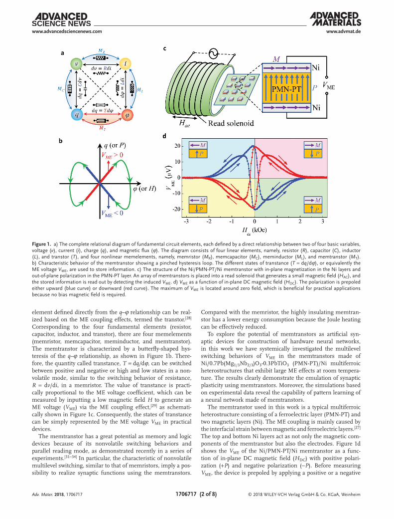
The VME switching behavior under electric pulses is analogous to the information transmission characteristics of biological synapses. Figure 2a shows a typical schematic illustration
of a biological synapse. A synapse is a conjunction of two neuron cells, named preneuron and postneuron. Under an external stimulus, spikes or action potentials from the pre-neuron are transmitted through synapse to the postneuron and generate excitatory postsynaptic potentials (EPSP) or inhibi-tory postsynaptic potentials (IPSP), together with the synaptic weight updates.[33] The information storage and learning of human brains are exactly a consequence of changes in the syn-aptic weight. Here, the artificial synapse based on memtran-stors is achieved by regarding the transtance value as the synaptic weight and the generated increasing/decreasing VME as the EPSP/IPSP. The applied voltage pulses play the roles of the pre and postspikes that act on a memtranstor to modulate the transtance (i.e., synaptic weight), which is assessed by the detec-tion of VME (i.e., EPSP/IPSP). Therefore, the increasing VME (EPSP) and decreasing VME (IPSP), as shown in Figures 2b,c, indicates the potentiation and depression of the synaptic weight, respectively, that is, synaptic plasticity. In biological systems, the synaptic plasticity can be divided into short-term plasticity and long-term plasticity according to the retention time of the synaptic weight, corresponding to the short-term memory and long-term memory of brain, respectively.[35–37] For the Ni/PMN-PT/Ni memtranstor, the obtained transtance states are quite stable with time. Therefore, the EPSP and IPSP, as shown in Figures 2b,c, can be classed as long-term plasticity, corresponding to the long-term potentiation (LTP) and long-term depression (LTD), respectively.
A well-known theory based on synaptic plasticity is Hebbian learning, which suggests that the synaptic weight is modulated in accordance to neural activities in preneuron and postneuron cells.[38] In this form, one of the most important learning rule is spiking-time-dependent plasticity (STDP).[39] STDP establishes the synaptic weight adjustment according to the timing of the fired spikes by connected neurons. According to this rule, the synapse potentiates (EPSP or increase of VME) if presynaptic spikes precede postsynaptic spikes repeatedly, and the synapse depresses (IPSP or decrease of VME) if postsynaptic spike pre-cedes presynaptic spike repeatedly. The precise pre and post-spike timing window controls the sign and magnitude of syn-aptic weight modulation.
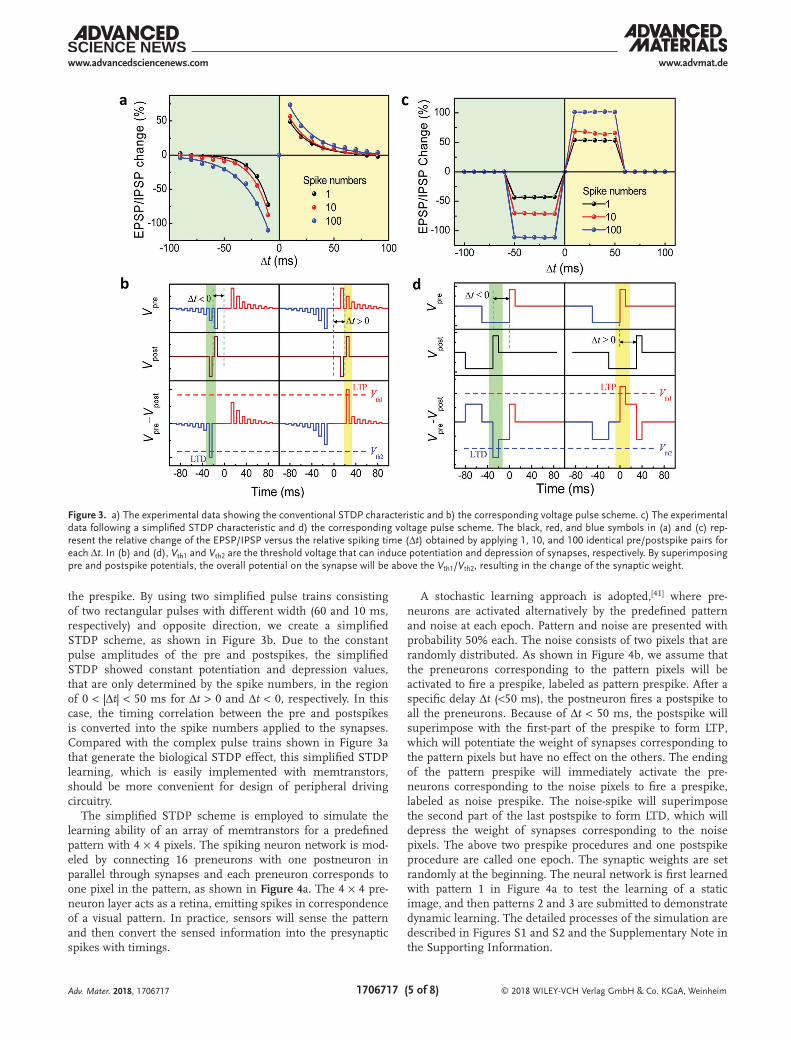
Based on the plasticity behaviors of the Ni/PMN-PT/Ni memtranstors as a function of pulse amplitude and repeti-tion, STDP is emulated by engineering the pre and postspike superimpositions. As shown in the lower panel of Figure 3a, the prespike is shaped as a pulse train, consisting of the depres-sion (negative voltage) pulses (width = 10 ms) with amplitude increasing from Vpre = −1 to −25 V and potentiation (positive voltage) pulses with amplitude decreasing from 25 to 1 V. The time spacing between two pulses is kept constant (10 ms). The postspike consists of two rectangular pulses (width = 10 ms) with amplitude of Vpost = 25 and −25 V. The superimposition between the prespike and the postspike (Vpre −Vpost) defines the net programming voltage applied on the synapse at each point of time. For example, if a prespike is 20 ms before the postspike (Δt = 20 ms), then the positive part of the postspike will overlap with the second potentiation pulse. The overall potential on the synapse will be above the potentiation threshold (Vth1), resulting in an increase in synaptic weight. However, if the post-spike is 20 ms before the prespike (Δt = −20 ms), the negative
Adv. Mater. 2018, 1706717
© 2018 WILEY-VCH Verlag GmbH & Co. KGaA, Weinheim1706717 (4 of 8)
www.advmat.dewww.advancedsciencenews.com
part of the postspike will overlap with the second depression pulse. The overall potential on the synapse will be above the depression threshold (Vth2), resulting in a decrease in synaptic weight. The change ratio of the synaptic weight can be tuned by changing the action numbers of the identical pre/postspike pairs for each Δt. By repeating the pulse scheme with different Δt in the range from −90 to 90 ms, the overall STDP curves are obtained, as shown in the top panel of Figure 3a. The obtained STDP characteristics can be well fitted with exponential
decay functions and conform to the well-known biological syn-aptic system.[40]
In a real biological system, the STDP model should con-sider the exact value of Δt because an enhanced change in the synaptic weight occurs as Δt is decreased. In the memtranstor-based synapses, the VME change can be only dependent on the present VME value and the applied pulse numbers according to the experimental data in Figure 2c. Thus, the pulse train with increasing (or decreasing) amplitude is unnecessary for
Adv. Mater. 2018, 1706717
Figure 2. a) Schematic illustration of biological neurons and synapses. Right inset: the information transmission between neurons occurs via propa-gation of action potentials through the axon and release of neurotransmitters, which causes excitatory postsynaptic potentials (EPSP) and inhibitory postsynaptic potentials (IPSP) that would in turn propagate in the postsynaptic axon. Left inset: The memtranstor-based synapse transmits information by applying voltage pulses to change the polarization and subsequently change the ME coupling to produce the VME variation. The VME plays a role of either EPSP (increase of VME) or IPSP (decrease of VME) in the postsynaptic axon. b) The evolution of the EPSP/IPSP (i.e., VME) by applying trains of voltage pulses (bottom part) with a fixed time width of 10 ms spaced 100 s apart and increasing amplitude. The VME was measured at the pulse spacing. The insets in (b) present enlarged views of each obtained EPSP/IPSP that shows good stability and can last for a certain period of time (100 s for each step). c) The evolution of the EPSP/IPSP (i.e., VME) by applying voltage pulses with 10 ms width and a constant amplitude of E = 2.5 kV cm−1.
© 2018 WILEY-VCH Verlag GmbH & Co. KGaA, Weinheim1706717 (5 of 8)
www.advmat.dewww.advancedsciencenews.com
the prespike. By using two simplified pulse trains consisting of two rectangular pulses with different width (60 and 10 ms, respectively) and opposite direction, we create a simplified STDP scheme, as shown in Figure 3b. Due to the constant pulse amplitudes of the pre and postspikes, the simplified STDP showed constant potentiation and depression values, that are only determined by the spike numbers, in the region of 0 < |Δt| < 50 ms for Δt > 0 and Δt < 0, respectively. In this case, the timing correlation between the pre and postspikes is converted into the spike numbers applied to the synapses. Compared with the complex pulse trains shown in Figure 3a that generate the biological STDP effect, this simplified STDP learning, which is easily implemented with memtranstors, should be more convenient for design of peripheral driving circuitry.
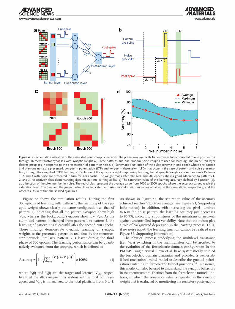
The simplified STDP scheme is employed to simulate the learning ability of an array of memtranstors for a predefined pattern with 4 × 4 pixels. The spiking neuron network is mod-eled by connecting 16 preneurons with one postneuron in parallel through synapses and each preneuron corresponds to one pixel in the pattern, as shown in Figure 4a. The 4 × 4 pre-neuron layer acts as a retina, emitting spikes in correspondence of a visual pattern. In practice, sensors will sense the pattern and then convert the sensed information into the presynaptic spikes with timings.
A stochastic learning approach is adopted,[41] where pre-neurons are activated alternatively by the predefined pattern and noise at each epoch. Pattern and noise are presented with probability 50% each. The noise consists of two pixels that are randomly distributed. As shown in Figure 4b, we assume that the preneurons corresponding to the pattern pixels will be activated to fire a prespike, labeled as pattern prespike. After a specific delay Δt (<50 ms), the postneuron fires a postspike to all the preneurons. Because of Δt < 50 ms, the postspike will superimpose with the first-part of the prespike to form LTP, which will potentiate the weight of synapses corresponding to the pattern pixels but have no effect on the others. The ending of the pattern prespike will immediately activate the pre-neurons corresponding to the noise pixels to fire a prespike, labeled as noise prespike. The noise-spike will superimpose the second part of the last postspike to form LTD, which will depress the weight of synapses corresponding to the noise pixels. The above two prespike procedures and one postspike procedure are called one epoch. The synaptic weights are set randomly at the beginning. The neural network is first learned with pattern 1 in Figure 4a to test the learning of a static image, and then patterns 2 and 3 are submitted to demonstrate dynamic learning. The detailed processes of the simulation are described in Figures S1 and S2 and the Supplementary Note in the Supporting Information.
Adv. Mater. 2018, 1706717
Figure 3. a) The experimental data showing the conventional STDP characteristic and b) the corresponding voltage pulse scheme. c) The experimental data following a simplified STDP characteristic and d) the corresponding voltage pulse scheme. The black, red, and blue symbols in (a) and (c) rep-resent the relative change of the EPSP/IPSP versus the relative spiking time (Δt) obtained by applying 1, 10, and 100 identical pre/postspike pairs for each Δt. In (b) and (d), Vth1 and Vth2 are the threshold voltage that can induce potentiation and depression of synapses, respectively. By superimposing pre and postspike potentials, the overall potential on the synapse will be above the Vth1/Vth2, resulting in the change of the synaptic weight.
© 2018 WILEY-VCH Verlag GmbH & Co. KGaA, Weinheim1706717 (6 of 8)
www.advmat.dewww.advancedsciencenews.com
Figure 4c shows the simulation results. During the first 300 epochs of learning with pattern 1, the mapping of the syn-aptic weight shows clearly the same configuration as that of pattern 1, indicating that all the pattern synapses show high VME, whereas the background synapses show low VME. As the submitted pattern is changed from pattern 1 to pattern 2, the learning of pattern 2 is successful after the second 300 epochs. These findings demonstrate dynamic learning of synaptic weights to the presented pattern in real time by the memtran-stor network. Similarly, pattern 3 is learnt during the third phase of 300 epochs. The learning performance can be quanti-tatively evaluated from the accuracy, which is defined as
Accuracy 1 100%t i
2
1
V i V i
ni
n∑ ( )( ) ( )= −
−
×=
(1)
where Vt(i) and Vi(i) are the target and learned VME, respec-tively, at the ith synapse in a system with a total of n syn-apses, and VME is normalized to the total plasticity from 0 to 1.
As shown in Figure 4d, the saturation value of the accuracy achieved reaches 91.3% on average (see Figure S3, Supporting Information). In addition, with increasing the pixel numbers to 6 in the noise pattern, the learning accuracy just decreases to 86.9%, indicating a robustness of the memtranstor network against uncontrolled input variability. Note that the noises play a role of background depression in the learning process. Thus, if no noise input, the learning function cannot be realized (see Figure S6, Supporting Information).
The physical process underlying the multilevel transtance (i.e., VME) switching in the memtranstors can be ascribed to the evolution of the ferroelectric domain configuration in the PMN-PT single crystal. Boyn et al. have systematically studied the ferroelectric domain dynamics and provided a well-estab-lished nucleation-limited model to describe the gradual polari-zation switching in ferroelectric tunnel junctions.[14] In essence, this model can also be used to understand the synaptic behaviors in the memtranstors. Distinct from the ferroelectric tunnel junc-tions, in which the resistance value is regarded as the synaptic weight that is evaluated by monitoring the excitatory postsynaptic
Adv. Mater. 2018, 1706717
Figure 4. a) Schematic illustration of the simulated neuromorphic network. The preneuron layer with 16 neurons is fully connected to one postneuron through 16 memtranstor synapses with synaptic weight wi. Three patterns and one random noise image are used for learning. The preneuron layer derives prespikes in response to the presentation of pattern or noise. b) Schematic illustration of the pulse scheme in one epoch where one pattern and then one noise are presented. Long-term potentiation (LTP) and long-term depression (LTD) that occur in the case of pattern and noise presenta-tion, through the simplified STDP learning. c) Evolution of the synaptic weight map during learning. Initial synaptic weights are set randomly. Patterns 1, 2, and 3 with noise are presented in turn for 300 epochs. The weight maps after 300, 600, and 900 epochs show a good adherence to patterns 1, 2, and 3, respectively, thus demonstrating dynamic pattern learning ability. d) The saturation value of the learning accuracy, defined by Equation (1), as a function of the pixel number in noise. The red circles represent the average value from 1000 to 2000 epochs where the accuracy values reach the saturation level. The blue and the green dashed lines indicate the maximum and minimum values obtained in the simulations, respectively, and the other results lie within the shaded cyan area.
© 2018 WILEY-VCH Verlag GmbH & Co. KGaA, Weinheim1706717 (7 of 8)
www.advmat.dewww.advancedsciencenews.com
Adv. Mater. 2018, 1706717
current (EPSC), the synaptic weight of memtranstor-based syn-apses is represented by the EPSP because voltage signals are directly generated during the reading process. In biology, the EPSP is closer to the real characteristics of nerve cells, such as the membrane potential of the soma than the EPSC.[42]
To assess the energy consumption of the memtranstor net-work, we have calculated the energy for both weight reading and weight change per synapse during the memtranstor working cycle. Because PMN-PT is a good insulator and the leakage cur-rent is negligible, the most significant contribution to energy consumption of weight change is the ferroelectric polarization inversion by electric field. The energy density Jp for ferroelectric polarization inversion can be roughly estimated from Jp = 2PsEa, where Ps is the maximum intensity of polarization, and Ea is the applied electric field. According to the saturated polarization (≈40 µC cm−2) of PMN-PT and the electric field (2.75 kV cm−1) we used in this study, the energy density for weight change per synapse is calculated to be 0.22 J cm−3. Thus, we project an energy cost of 0.22 pJ for the weight change of a 1 µm × 1 µm × 1 µm memtranstor, which is several orders of magnitude lower than that of the synapses based on conventional CMOS circuit (≈900 pJ per stimulation).[7] Regarding the weight reading, although the operation mode of the memtranstor is similar to traditional ferroelectric random access memory, the polarization change and rewriting process are not required during the VME reading, that is, the readout is nondestructive. Therefore, the main energy consumption is contributed by the read solenoid, which generates Hac for the VME detection. The energy density Jm of the read solenoid can be estimated by Jm =B2/2 µ, where B is the required magnetic field and µ is vacuum permeability. Thus, the magnetic field (2 Oe) we used for VME reading in this study amounts to 2 J cm−3. Note that, for the memtranstor devices with high density arrays, it will be difficult to apply a magnetic field to each memtranstor unit. A feasible approach is to share one mag-netic field. Although this approach will enlarge the volume of the magnetic field, that is, the energy consumption, the average energy consumption per memtranstor unit, depending on the storage density of the devices, could be reduced.
In conclusion, we implemented synaptic plasticity in the memtranstors made of Ni/PMN-PT/Ni multiferroic hetero-structures that enable the nonvolatile continuous change of the ME coupling voltage. As a proof-of-concept, we demonstrated that by engineering the applied electric pulse which serves as the action potentials, the memtranstance, which is presented by ME coupling voltage and serves as synaptic weight, can perform the LTP, LTD, and STDP of biological synapses. The learning ability of the memtranstor network was demonstrated through a stochastic pattern learning. Combining the advantages of low-power consumption of weight change and nondestructive weight readout, such memtranstor devices have the potential to realize energy-efficient neural networks for building neuromor-phic computing systems.
Experimental SectionFabrication of the Devices: The memtranstors were prepared by
depositing Ni on both sides of PMN-PT (110) single crystals by magnetic sputtering to form Ni/PMN-PT/Ni heterostructures, as illustrated in Figure 1b. The size of PMN-PT single crystal is 5 × 2 mm. The
thicknesses of PMN-PT (110) single crystal and the Ni films are 0.2 mm and 1 µm, respectively. The ME coupling is mainly caused by the interfacial strain between the magnetic and ferroelectric layers. The top and bottom Ni layers act as not only the magnetic components of the memtranstor but also the electrodes for the output of VME.
Measurements of the ME Voltage: A conventional dynamic technique was employed to measure the VME (see Figure S1, Supporting Information). A small AC magnetic field HAC at a frequency of 10 kHz, generated by an AC source (Keithley 6221) to a solenoid, in the presence of a simultaneous DC bias magnetic field, was applied in plane to the devices. In response, the change in the electric signal (VAC =Vx + iVy) across the sample resulting from the applied HAC was recorded using a lock-in amplifier (Stanford Research SR830) synchronized with the AC current source. To switch or prepole the electric polarization of PMN-PT (110), a sourcemeter(Keithley 6517B) was used to apply voltage pulse across the electrodes. The sample was plugged into an Oxford TeslatronPT superconducting magnet system, which supplies the DC magnetic field. All the measurements were performed at room temperature. To realize automatic measurements, a switcher (Keithley 7001) is used to control the pulse application and the VME reading operations in a program sequence.
Supporting InformationSupporting Information is available from the Wiley Online Library or from the author.
AcknowledgementsThis work was supported by the National Nature Science Foundation of China (Grant Nos. 11534015, 51671213, 51725104, and 51625101), the National Key Research Program of China (Grant No. 2016YFA0300701), and the Chinese Academy of Sciences (Grant No. XDB07030200).
Conflict of InterestThe authors declare no conflict of interest.
Keywordsmagnetoelectric coupling, memtranstors, multilevel switching, synaptic devices, synaptic plasticity
Received: November 16, 2017Revised: December 18, 2017
Published online:
[1] J. Backus, Commun. ACM 1978, 21, 613.[2] G. Indiveri, S. H. Liu, Proc. IEEE 2015, 103, 1379.[3] D. S. Jeong, I. Kim, M. Ziegler, H. Kohlstedt, RSC Adv. 2013, 3,
3169.[4] C. Mead, Proc. IEEE 1990, 78, 1629.[5] M. Mahowald, R. A. Douglas, Nature 1991, 354, 515.[6] J. H. B. Wijekoon, P. Dudek, Neural Networks 2008, 21, 524.[7] G. Indiveri, E. Chicca, R. A. Douglas, IEEE Trans. Neural Networks
2006, 17, 211.[8] L. Chua, Appl. Phys. A: Mater. Sci. Process. 2011, 102, 765.[9] J. J. Yang, D. B. Strukov, D. R. Stewart, Nat. Nanotechnol. 2013,
8, 13.

© 2018 WILEY-VCH Verlag GmbH & Co. KGaA, Weinheim1706717 (8 of 8)
www.advmat.dewww.advancedsciencenews.com
Adv. Mater. 2018, 1706717
[10] D. Kuzum, R. G. D. Jeyasingh, B. Lee, H. S. P. Wong, Nano Lett. 2012, 12, 2719.
[11] T. Tuma, A. Pantazi, M. L. Gallo, A. Sebastian, E. Eleftheriou, Nat. Nanotechnol. 2016, 11, 693.
[12] G. W. Burr, R. M. Shelby, S. Sidler, C. Nolfo, J. Jang, I. Boybat, R. S. Shenoy, P. Narayanan, K. Virwani, E. U. Giacometti, B. N. Kurdi, H. Hwang, IEEE Trans. Electron Devices 2015, 62, 3498.
[13] Y. Kaneko, Y. Nishitani, M. Ueda, IEEE Trans. Electron Devices 2014, 61, 2827.
[14] S. Boyn, J. Grollier, G. Lecerf, B. Xu, N. Locatelli, S. Fusil, S. Girod, C. Carrétéro, K. Garcia, S. Xavier, J. Tomas, L. Bellaiche, M. Bibes, A. Barthélémy, S. Saïghi, V. Garcia, Nat. Commun. 2017, 8, 14736.
[15] P. Krzysteczko, J. Münchenberger, M. Schäfers, G. Reiss, A. Thomas, Adv. Mater. 2012, 24, 762.
[16] J. Grollier, D. Querlioz, M. D. Stiles, Proc. IEEE 2016, 104, 2024.[17] C. O. Avci, M. Mann, A. J. Tan, P. Gambardella, G. S. D. Beach,
Appl. Phys. Lett. 2017, 110, 203506.[18] S. H. Jo, T. Chang, I. Ebong, B. B. Bhadviya, P. Mazumder, W. Lu,
Nano Lett. 2010, 10, 1297.[19] F. Alibart, E. Zamanidoost, D. B. Strukov, Nat. Commun. 2013, 4,
2072.[20] S. Yu, B. Gao, Z. Fang, H. Yu, J. Kang, H. S. P. Wong, Adv. Mater.
2013, 25, 1774.[21] C. S. Yang, D. S. Shang, Y. S. Chai, L. Q. Yang, B. G. Shen, Y. Sun,
Phys. Chem. Chem. Phys. 2014, 19, 4190.[22] C. S. Yang, D. S. Shang, N. Liu, G. Shi, X. Shen, R. C. Yu, Y. Q. Li,
Y. Sun, Adv. Mater. 2017, 29, 1700906.[23] Z. Wang, S. Joshi, S. E. Savel’ev, H. Jiang, R. Midya, P. Lin, M. Hu,
N. Ge, J. P. Strachan, Z. Li, Q. Wu, M. Barnell, G. L. Li, H. L. Xin, R. S. Williams, Q. Xia, J. J Yang, Nat. Mater. 2017, 16, 101.
[24] A. Serb, J. Bill, A. Khiat, R. Berdan, R. Legenstein, T. Prodromakis, Nat. Commun. 2016, 7, 12611.
[25] P. Yao, H. Wu, B. Gao, S. B. Eryilmaz, X. Huang, W. Zhang, Q. Zhang, N. Deng, L. Shi, J. S. P. Wong, H. Qian, Nat. Commun. 2017, 8, 15199.
[26] Y. Yang, M. Yin, Z. Yu, Z. Wang, T. Zheng, Y. Cai, W. D. Lu, R. Huang, Adv. Electron. Mater. 2017, 3, 1700032.
[27] C. Song, B. Cui, F. Li, X. Zhou, F. Pan, Prog. Mater. Sci. 2017, 87, 33.
[28] D. S. Shang, Y. S. Chai, Z. X. Cao, J. Lu, Y. Sun, Chin. Phys. B 2015, 25, 068402.
[29] L. O. Chua, IEEE Trans. Circuit Theory 1971, 18, 507.[30] N. D. Mathur, Nature 2008, 455, E13.[31] J. X. Shen, J. Z. Cong, Y. S. Chai, D. S. Shang, S. P. Shen, K. Zhai,
Y. Tian, Y. Sun, Phys. Rev. Appl. 2016, 6, 021001.[32] J. X. Shen, D. S. Shang, Y. S. Chai, Y. Wang, J. Z. Cong, S. P. Shen,
L. Q. Yan, W. H. Wang, Y. Sun, Phys. Rev. Appl. 2016, 6, 064028.[33] J. X. Shen, J. Z. Cong, D. S. Shang, Y. S. Chai, S. P. Shen, K. Zhai,
Y. Sun, Sci. Rep. 2016, 6, 34473.[34] P. P. Lu, D. S. Shang, J. X. Shen, Y. S. Chai, C. S. Yang, K. Zhai,
J. Z. Cong, S. P. Shen, Y. Sun, Appl. Phys. Lett. 2016, 109, 252902.
[35] L. F. Abbott, S. B. Nelson, Nat. Neurosci. 2000, 3, 1178.[36] T. Ohno, T. Hasegawa, T. Tsuruoka, K. Terabe, J. K. Gimzewski,
M. Aono, Nat. Mater. 2011, 10, 591.[37] T. Chang, S. H. Jo, W. Lu, ACS Nano 2011, 5, 7669.[38] D. O. Hebb, The Organization of Behavior, Wiley and Sons,
New York 1949.[39] N. Caporale, Y. Dan, Annu. Rev. Neurosci. 2008, 31, 25.[40] G. Q. Bi, M. M. Poo, J. Neurol. 1998, 18, 10464.[41] S. Ambrogio, N. Ciocchini, M. Laudato, V. Milo, A. Pirovano,
P. Fantini, D Ielmini, Front. Neurosci. 2016, 10, 56.[42] J. C. Eccles, The Physiology of Nerve Cells, Johns Hopkins Press,
Baltimore, MD, USA 1968.