miniskiip dual utilization, pcb design …...... pcb design recommendations and test results ......
TRANSCRIPT

© by SEMIKRON / Application Note / AN1402 / 2014-12-19
PROMGT.1023/ Rev.3/ Template Application Note
Page 1/14
MiniSKiiP Dual – Utilization, PCB Design
Recommendations and Test Results
1. General ..................................................................................................................................... 1
2. Test Phase 1 – One-Module-PCBs ................................................................................................. 2 2.1 PCB layout ........................................................................................................................... 2 2.2 High power connectors ........................................................................................................... 3 2.3 Measurement setup and conditions .......................................................................................... 4 2.4 Measurement results ............................................................................................................. 5
3. Test Phase 2 – Three-Phase-PCB .................................................................................................. 7 3.1 PCB layout ........................................................................................................................... 7 3.2 Measurement setup and conditions .......................................................................................... 9 3.3 Measurement results ............................................................................................................. 9
4. Recommendations for a PCB Design ............................................................................................ 11 4.1 Summary ........................................................................................................................... 11 4.2 PCB recommendations ......................................................................................................... 11
This application note provides information on the SEMIKRON power module MiniSKiiP Dual which contains a
standard two-level halfbridge (two IGBTs and antiparallel freewheeling diodes; one phase leg per module). The reader will learn about the high power tests that have been performed with the MiniSKiiP Dual. Some recommendations concerning the PCB design will be given as well. However, the information given is not exhaustive and the responsibility for a proper and reliable design remains with the user.
1. General
The MiniSKiiP Dual inherits only one two-level halfbridge consisting of two IGBTs and two antiparallel
freewheeling diodes. It comes in two different housing sizes (size 2 and size 3, Figure 1). Due to the optimized halfbridge layout it is possible to reach nominal chip currents of up to 300 A (housing size 3) using 1200V semiconductors. Depending on switching frequency and cooling performance it is possible to reach up to 150A of output RMS current with this type of module. The MiniSKiiP modules come with extremely reliable spring contacts for both auxiliary and power
connection. No complicated copper busbar design is necessary any more as all connections are made to the PCB. The printed circuit board carries not only the main DC and AC current but can also be assembled with
all the required circuitry like gate resistors, driving units or even microcontrollers. In order to diffuse doubts concerning the high announced current rating of the MiniSKiiP Dual modules and to prove that this high current can be conducted across standard PCBs, adaptor PCBs to contact the modules have been produced. Tests have been performed with two types of adaptor boards: small PCBs contacting only one module as well as one large PCB with a three-phase inverter system contacting three modules and DC-link capacitors.
Different high power connectors between PCB and load have been tested in one go. Thermocouples have been fixed to the heatsink for reference measurement at the PCB hotspot (around the hottest module) and at the air exit of the heatsink (last heatsink at test phase 1 or phase V at test phase 2
Application Note
AN1402 Revision: 02
Issue date: 2014-12-19
Prepared by: Ingo Staudt
Approved by: Peter Beckedahl
Keyword: MiniSKiiP Dual, PCB design, high power PCB

© by SEMIKRON / Application Note / AN1402 / 2014-12-19 Page 2/14
respectively). These measurements show that the temperature deviation between the module’s built-in temperature sensor and the heatsink is below 5K. Further the accuracy of the thermo camera measurement could be determined. It is 1.3K in each direction. As the measured temperatures range between 50°C and 10°C the error is below 3%, so the deviation may be neglected. Based on this experience the heatsink temperature is referred to the module’s built-in temperature sensor
only. The results are presented in this application note.
Figure 1: MiniSKiiP Dual housing size 2 (left) and housing size 3 (right)
2. Test Phase 1 – One-Module-PCBs
In a first attempt PCBs contacting only one MiniSKiiP module each have been produced.
2.1 PCB layout
Using one PCB per MiniSKiiP module offers the opportunity to try out different technologies. In this test
SEMIKRON produced 2-layer boards with a copper thickness of 210µm and 4-layer boards with a copper strength of 105µm per layer. The PCB layout was chosen identical for both technologies, hence the copper cross section as well.
Figure 2: MiniSKiiP Dual housing pressure lid
Figure 2 shows the top (left) and bottom (right) view of a pressure lid for the MiniSKiiP size 3 module. The photo shall illustrate that there are many pressure points where mechanical force is conducted from the
pressure lid to the PCB. To achieve an equal force across the module the PCB height must be constant underneath the lid. So it is necessary to place copper pads wherever one of the pins is located. For further information please refer to the technical explanations of MiniSKiiP and MiniSKiiP Dual. Two of those pads are marked red in Figure 3.

© by SEMIKRON / Application Note / AN1402 / 2014-12-19 Page 3/14
Figure 3: Photo (left) and drawing (right) of the top layer
Figure 3 shows a photo of the top side of the 4-layer adaptor PCB for one MiniSKiiP module (left) and the drawing of the same board.
Figure 4: Drawing of inner layers (left) and bottom layer (right)
Figure 4 shows the drawings of the inner layers (left; exemplarily only layer 2, but layer 3 is congruent)
and the bottom layer (right). It is obvious that there is only a minor reduction in the cross section of the AC top layer where gate and emitter spring contacts require some distance to AC potential in order to maintain creepage and clearance distances. Hence the maximum available cross section has been used to conduct current and to dissipate heat via radiation at the AC side. To further increase the heat dissipation the copper areas at the DC side has been enlarged beyond the spring contact area.
The layers of the 2-layer PCB are identical to top and bottom layers of the 4-layer PCB.
2.2 High power connectors
Four different types of high power connectors from PCB to cable have been tested: - Simple tin-plated holes for connecting cable shoes (Figure 5, left) - Two press-fit bolts (Würth Electronic, PowerOne Pin M6, 25 pins, 150A @ 85°C) (Figure 5, right) - Two SMD bolts (Würth Electronic, PowerPlus SMD, with screw M6x16, 130A @ 85°C) (Figure 6, left)
- A 4-fold connector block (PHOENIX MKDSP 25/4-15,00, 75A per contact @ 85°C) (Figure 6, right) As PCB temperatures up to 100°C were expected, two of each contact types have been installed (4-fold instead of 2-fold connector block).

© by SEMIKRON / Application Note / AN1402 / 2014-12-19 Page 4/14
Figure 5: Tinplated mounting hole (left) and press-fit bolt (right)
Figure 6: SMD bolt (left) and 4-fold connector block (right)
The white-colored MOLEX plugs allow for easy connection of driver circuitry and temperature sensors. They are not subject to this examination and may be replaced by any other suitable connector if required.
2.3 Measurement setup and conditions
Three PCBs were tested in real 4Q inverter operation. Every PCB connected one SKiiP38GB12T4V1 which were mounted on separate air coolers each and connected to a SEMIKRON standard DC-link. The three air coolers were chosen just so big that they fit next to each other. They are cooled by one strong radial blower. Standard SEMIKRON drivers were connected to the modules via twisted wires. The air condition in the 4Q test bench was switched off to avoid cool air flowing across and cooling down the PCBs. The temperature increase was monitored via the ambient temperature measurement. More
thermocouples have been fixed for reference measurements to the air exit of the last heat sink, the air entrance of the first heatsink and the pressure lid of the module on the last heatsink. The white paint was required to receive reliable data from the infrared thermo camera measurement. The test setup is shown in Figure 7.

© by SEMIKRON / Application Note / AN1402 / 2014-12-19 Page 5/14
Figure 7: 3-phase setup with fan and drivers (left) and last heatsink with thermocouples (right)
During the test only PCBs with bolts and the PHOENIX connector have been used. The option with the tin-plated holes at the AC-side has not been tested as there were already similar connectors at the DC-side. Additionally the holes are thermally better coupled to PCB and power wiring and so would perform better than all other kinds of connectors anyway. The inverter test started with the lowest chosen AC current (100A), which was set for one hour to allow a thermal balance of test and measurement equipment. Every further current increase was kept for 30
minutes as after approx. 20 minutes a steady state condition was reached. The first test series has been performed with the 4-layer PCBs up to an AC current of 200A. In the first run both bolts per PCB and all four PHOENIX clamps have been connected. In the second run the number of AC
contacts has been halved; one bolt or two clamps (the middle ones) respectively. The second test series has been performed in the same way but with the 2-layer PCBs. In difference to the first run, the mounting order of the three PCBs has been swapped. In the 4-layer run press-fit bolts, SMD bolts and PHOENIX clamps have been mounted from left to right, in the 2-layer run PHOENIX clamps, SMD
bolts and press-fit bolts have been used from left to right. The “left side” is close to the air entrance and the blower whereas “right side” is at the exit of the hot air. For the third test series the 4-layer PCBs have been used again (same mounting order as in the first test) with the half amount of contacts and even higher AC currents up to 260A. At AC currents between 100A and 200A the switching frequency was set to 2kHz, above 200A it has been reduced to 1.5kHz. For getting realistic results the operating conditions were set to: DC voltage of 700V, AC voltage of 400V and a cos of 0.8.
The switching frequency was chosen very low to allow for higher AC currents as this test was about the current capability of the PCB only.
2.4 Measurement results
Figure 8 shows steady state infrared images of the inverter running at 150A or 200A respectively. The
upper two images show the 2-layer PCB and the lower images the 4-layer PCB. Swapping the boards’ order
did not show any change in results either. The temperature scale for one current value is identical, so it gets obvious that the PCB technology does not affect the self-heating of the boards.

© by SEMIKRON / Application Note / AN1402 / 2014-12-19 Page 6/14
Figure 8: 150A (left) and 200A (right) with 2-layer (top) and 4-layer (bottom) PCB
Table 1 shows the measurement results in steady state condition for 2-layer and 4-layer PCBs at 150A and 200A. Additionally the 260A measurement result with the 4-layer board shows that even extremely high
currents are possible.
Table 1: Temperature measurements in steady state condition
Sample IAC Tamb Tsensor TIR,max T of Tsensor
vs. TIR,max
- [A] [°C] [°C] [°C] [K]
2-layer 150 28.6 53.0 45.0 8.0
200 30.2 67.0 55.0 12.0
4-layer
150 29.7 53.0 45.0 8.0
200 30.8 68.0 55.0 13.0
260 30.7 87.0 70.0 17.0
Tamb is the ambient temperature which has been measured by the test cabinet. TIR,max is the maximum PCB surface temperature around the module on the right side coming from the thermo camera measurement. Tsensor is the measured value of temperature sensor inside the module. It represents the heatsink
temperature. The T in the last column in Table 1 is the temperature difference between heatsink and the maximum PCB
temperature. Up to 200A it stays between 8K and 13K and even at 260A output current does not exceed 17K. In all operating points the PCB temperature is below that of the heatsink. All tests have been performed with both full and half number of power connectors with no impact on the PCB temperature.
© by SEMIKRON / Application Note / AN1402 / 2014-12-19 Page 7/14
After having finished the measurements the tested modules and PCBs have been investigated. There have been no discolorations in the spring contact area which would have indicated thermal overload. So obviously both PCB technologies can easily conduct the highest with the MiniSKiiP Dual module possible current. A special high current PCB (e.g. wire-laid technology) has not been tested and, from the measurement results’ point of view, is not required.
For the announced AC current of 150A one press-fit bolt is sufficient at an ambient temperature of 30°C.
3. Test Phase 2 – Three-Phase-PCB
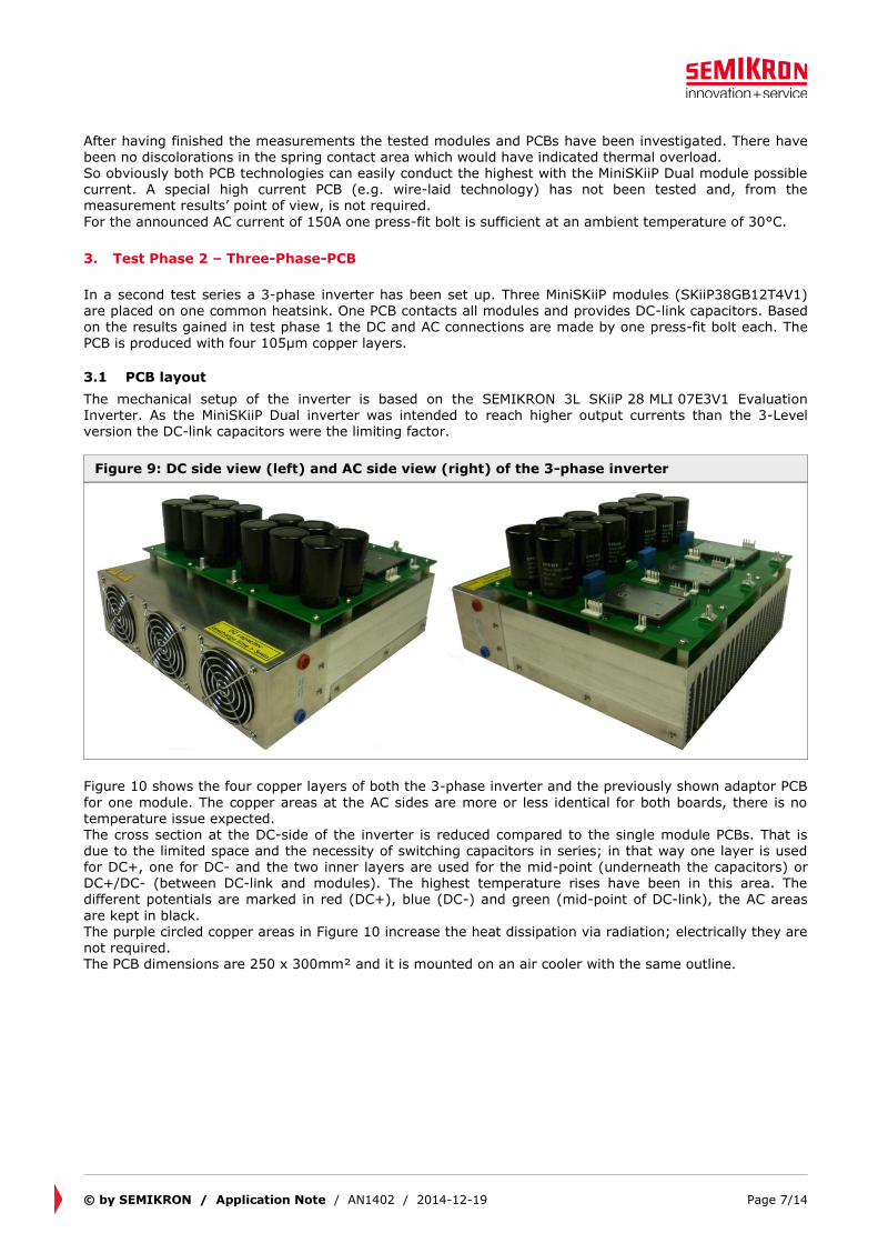
In a second test series a 3-phase inverter has been set up. Three MiniSKiiP modules (SKiiP38GB12T4V1) are placed on one common heatsink. One PCB contacts all modules and provides DC-link capacitors. Based on the results gained in test phase 1 the DC and AC connections are made by one press-fit bolt each. The PCB is produced with four 105µm copper layers.
3.1 PCB layout
The mechanical setup of the inverter is based on the SEMIKRON 3L SKiiP 28 MLI 07E3V1 Evaluation
Inverter. As the MiniSKiiP Dual inverter was intended to reach higher output currents than the 3-Level version the DC-link capacitors were the limiting factor.
Figure 9: DC side view (left) and AC side view (right) of the 3-phase inverter
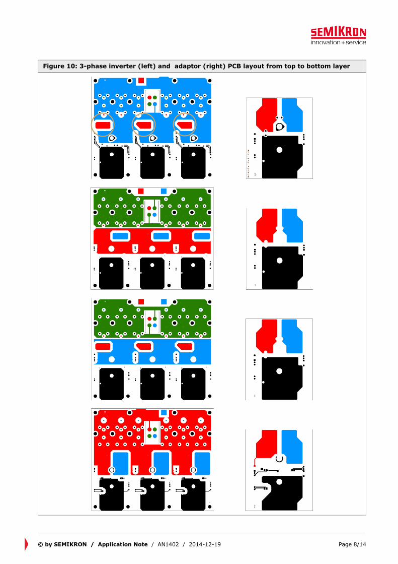
Figure 10 shows the four copper layers of both the 3-phase inverter and the previously shown adaptor PCB
for one module. The copper areas at the AC sides are more or less identical for both boards, there is no temperature issue expected. The cross section at the DC-side of the inverter is reduced compared to the single module PCBs. That is due to the limited space and the necessity of switching capacitors in series; in that way one layer is used for DC+, one for DC- and the two inner layers are used for the mid-point (underneath the capacitors) or DC+/DC- (between DC-link and modules). The highest temperature rises have been in this area. The different potentials are marked in red (DC+), blue (DC-) and green (mid-point of DC-link), the AC areas
are kept in black. The purple circled copper areas in Figure 10 increase the heat dissipation via radiation; electrically they are not required. The PCB dimensions are 250 x 300mm² and it is mounted on an air cooler with the same outline.
© by SEMIKRON / Application Note / AN1402 / 2014-12-19 Page 8/14
Figure 10: 3-phase inverter (left) and adaptor (right) PCB layout from top to bottom layer
© by SEMIKRON / Application Note / AN1402 / 2014-12-19 Page 9/14
3.2 Measurement setup and conditions
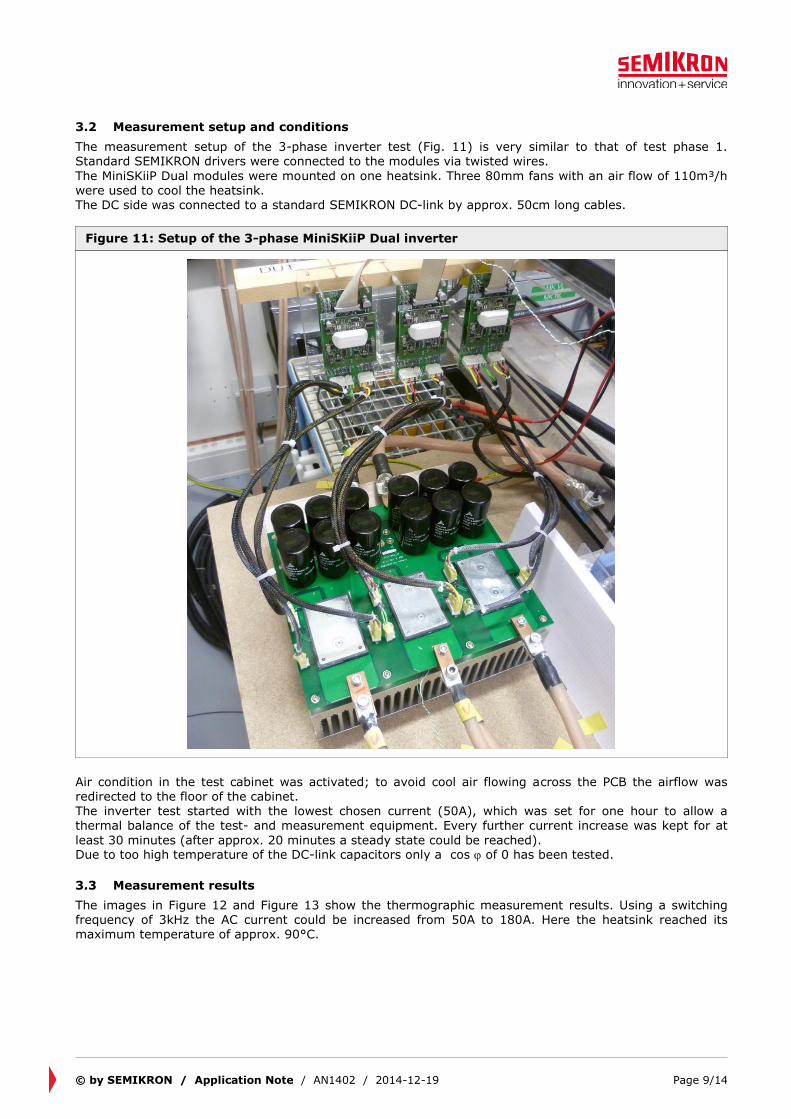
The measurement setup of the 3-phase inverter test (Fig. 11) is very similar to that of test phase 1. Standard SEMIKRON drivers were connected to the modules via twisted wires.
The MiniSKiiP Dual modules were mounted on one heatsink. Three 80mm fans with an air flow of 110m³/h were used to cool the heatsink. The DC side was connected to a standard SEMIKRON DC-link by approx. 50cm long cables.
Figure 11: Setup of the 3-phase MiniSKiiP Dual inverter
Air condition in the test cabinet was activated; to avoid cool air flowing across the PCB the airflow was redirected to the floor of the cabinet. The inverter test started with the lowest chosen current (50A), which was set for one hour to allow a thermal balance of the test- and measurement equipment. Every further current increase was kept for at
least 30 minutes (after approx. 20 minutes a steady state could be reached). Due to too high temperature of the DC-link capacitors only a cos of 0 has been tested.
3.3 Measurement results
The images in Figure 12 and Figure 13 show the thermographic measurement results. Using a switching frequency of 3kHz the AC current could be increased from 50A to 180A. Here the heatsink reached its maximum temperature of approx. 90°C.

© by SEMIKRON / Application Note / AN1402 / 2014-12-19 Page 10/14
Figure 12: 3-phase inverter at 50A (left) and 100A (right) at power factor = 0 and 3kHz switching frequency
Figure 13: 3-phase inverter at 150A (left) and 180A (right) at power factor = 0 and 3kHz switching frequency
In the final test, the switching frequency has been increased to a more application like value of 6kHz; here
the system can handle up to 125A (Figure 14, Table 2, bottom row). Above that value the heatsink does not provide sufficient cooling, so the current could not be increased further.
Figure 14: 3-phase inverter at 3kHz (left) and 6kHz (right) at power factor = 0 and 125A
The measurements show that the temperature around the middle module (phase V) and the temperature of the heatsink correlate.

© by SEMIKRON / Application Note / AN1402 / 2014-12-19 Page 11/14
Table 2: Temperature measurements in steady state condition
IAC Tamb Tsensor TIR,max T of Tsensor vs.
TIR,max
[A] [°C] [°C] [°C] [K]
50 22.0 40.0 32.0 8.0
100 22.0 54.0 50.0 4.0
125 22.0 63.0 59.0 4.0
150 22.0 78.0 74.0 4.0
180 22.0 95.0 94.0 1.0
125 (6kHz) 22.0 84.0 70.0 14.0
Table 2 shows the measured results: TIR,max is the maximum temperature of the PCB (around module of phase V) coming from the thermo camera measurement. Tamb is the ambient air temperature in front of the air inlet in a distance of 10cm to the fans. It was kept constant at 22°C by the air condition. Tsensor is the
temperature of the heatsink underneath the module of phase V. The results in show that the PCB temperature is very close to the heatsink temperature. At 180A the PCB hotspot reached a temperature of 94°C. In all tests the PCB is cooler than the heatsink, so obviously the PCB temperature is dominated by the heatsink temperature. As both PCB and heatsink have the same outline this correlation can be explained by thermal radiation The test showed that it is possible to conduct 180A across the PCB without destruction, deformation or
discoloration.
4. Recommendations for a PCB Design
4.1 Summary
Two test phases – one PCB per module on the one hand and a three-phase inverter system on the other – have been performed to push PCB and module to the thermal and electrical limits. The results show very clearly that a 300A rated module with spring contacts that conducts all the current from and into a PCB can easily be realized. The highest PCB temperature has always been lower than the heatsink temperature. 2-layer and 4-layer PCB behave identical. The 4-layer 3-phase inverter showed higher PCB temperatures due to reduced copper cross section. That was necessary because of the serial connection of capacitors. Further the current rating of the used press-fit connectors has been proven correct; there have been no
hotspots. The tests also showed that the module’s built-in temperature sensor measures the heatsink temperature with a deviation of only a few Kelvin.
4.2 PCB recommendations
In order to get good results from a very compact inverter design with MiniSKiiP Dual some recommendations should be taken into account:
- The usage of press-fit bolts depends on the current- and temperature rating and need to be chosen accordingly.
- The number of copper layers for the PCB design should be 4 or more, depending on the additional
electronic components that might be mounted next to the modules. - Capacitors which are able to withstand the full DC-link voltage make the serial connection
redundant and that increases the cross-section available for conducting the DC-current. - The allowed PCB temperature depends on the used material and may not be exceeded. However,
the module may not be exposed to temperatures above 125°C. - The PCB design around the module pressure lid needs to be in accordance to the Technical
Explanation of MiniSKiiP and MiniSKiiP Dual and the data sheets of the modules as it is mandatory to place pressure pads in the top layer that contact mechanically the pressure pins of the lid.
- A better cooling of the PCB can be achieved by using as many vias as possible and cooling areas so that heat can be dissipated by radiation.

© by SEMIKRON / Application Note / AN1402 / 2014-12-19 Page 12/14
Figure 1: MiniSKiiP Dual housing size 2 (left) and housing size 3 (right) ................................................. 2 Figure 2: MiniSKiiP Dual housing pressure lid ...................................................................................... 2 Figure 3: Photo (left) and drawing (right) of the top layer ..................................................................... 3 Figure 4: Drawing of inner layers (left) and bottom layer (right) ............................................................ 3 Figure 5: Tinplated mounting hole (left) and press-fit bolt (right) .......................................................... 4 Figure 6: SMD bolt (left) and 4-fold connector block (right)................................................................... 4 Figure 7: 3-phase setup with fan and drivers (left) and last heatsink with thermocouples (right) ............... 5 Figure 8: 150A (left) and 200A (right) with 2-layer (top) and 4-layer (bottom) PCB ................................. 6 Figure 9: DC side view (left) and AC side view (right) of the 3-phase inverter ......................................... 7 Figure 10: 3-phase inverter (left) and adaptor (right) PCB layout from top to bottom layer ...................... 8 Figure 11: Setup of the 3-phase MiniSKiiP Dual inverter ....................................................................... 9 Figure 12: 3-phase inverter at 50A (left) and 100A (right) at power factor = 0 and 3kHz switching
frequency ..................................................................................................................................... 10 Figure 13: 3-phase inverter at 150A (left) and 180A (right) at power factor = 0 and 3kHz switching frequency ..................................................................................................................................... 10 Figure 14: 3-phase inverter at 3kHz (left) and 6kHz (right) at power factor = 0 and 125A ...................... 10
Table 1: Temperature measurements in steady state condition ............................................................. 6 Table 2: Temperature measurements in steady state condition ........................................................... 11

© by SEMIKRON / Application Note / AN1402 / 2014-12-19 Page 13/14
Symbols and Terms
Letter Symbol Term
2L Two Level
3L Three Level
4Q 4 quadrant
AC Alternating Current
cos Power factor
DC Direct Current
DC+ Positive potential (terminal) of a direct voltage source
DC- Negative potential (terminal) of a direct voltage source
GB Half-bridge
IAC RMS output current of a device
IGBT Insulated Gate Bipolar Transistor
NTC Temperature sensor with negative temperature coefficient
PCB Printed Circuit Board
SMD Surface Mounted Device
Tamb Ambient / environment temperature
Tsensor Sensor temperature
A detailed explanation of the terms and symbols can be found in the "Application Manual Power Semiconductors" [2]
References
[1] www.SEMIKRON.com [2] A. Wintrich, U. Nicolai, W. Tursky, T. Reimann, “Application Manual Power Semiconductors”, ISLE
Verlag 2011, ISBN 978-3-938843-666 [3] M. Zurnacci, “MiniSKiiP Generation II – Technical Explanations”, Technical Explanation,
www.SEMIKRON.com, 2012 [4] T. Hürtgen, “MiniSKiiP Dual – Technical Explanations”, Technical Explanation, www.SEMIKRON.com,
2014 [5] I. Staudt, “Technical Explanation – 3L Evaluation Inverter”, Technical Explanation,
www.SEMIKRON.com, 2013

© by SEMIKRON / Application Note / AN1402 / 2014-12-19 Page 14/14
HISTORY
SEMIKRON reserves the right to make changes without further notice herein
DISCLAIMER
SEMIKRON reserves the right to make changes without further notice herein to improve reliability, function or design. Information furnished in this document is believed to be accurate and reliable. However, no representation or warranty is given and no liability is assumed with respect to the accuracy or use of such information, including without limitation, warranties of non-infringement of intellectual property rights of any third party. SEMIKRON does not assume any liability arising out of the application or use of any product or circuit described herein. Furthermore, this technical information may not be considered as an
assurance of component characteristics. No warranty or guarantee expressed or implied is made regarding delivery, performance or suitability. This document supersedes and replaces all information previously
supplied and may be superseded by updates without further notice. SEMIKRON products are not authorized for use in life support appliances and systems without the express written approval by SEMIKRON.
SEMIKRON INTERNATIONAL GmbH
P.O. Box 820251 • 90253 Nuremberg • Germany Tel: +49 911-65 59-234 • Fax: +49 911-65 59-262
[email protected] • www.semikron.com