mixed signal verification of a voltage regulator using a state space approach and the sv final
TRANSCRIPT
1
Mixed Signal Verification of a Voltage Regulator using a State Space Approach and the SV-‐DC extensions
Rajat Mitra Cadence Design Systems
270 Billerica Road Chelmsford, MA 01824 [email protected]
Abstract – Verification of mixed signal ICs has primarily been approached using a mixed signal simulator such as Cadence’s AMS Simulator (AMSD). The analog portions of the design are simulated using a combination of Verilog AMS and SPICE while the digital portions of the design are simulated using Verilog and System Verilog. The approach has traditionally been to verify connectivity and functional correctness at a high level between the digital and analog blocks. Recent trends in digital signal processing and control systems [1] have enabled implementing traditional analog functions digitally. This has resulted in significant digital content in mixed signal ICs. The traditional approach to mixed signal verification needs to be rethought. This paper proposes a robust methodology for the verification of mixed signal ICs with large digital content. The approach is digital centric and emphasizes a metric driven flow towards verification completion and confidence. The approach is illustrated by ways of a case study of a digital switch mode power supply (Buck Converter).
A. Introduction
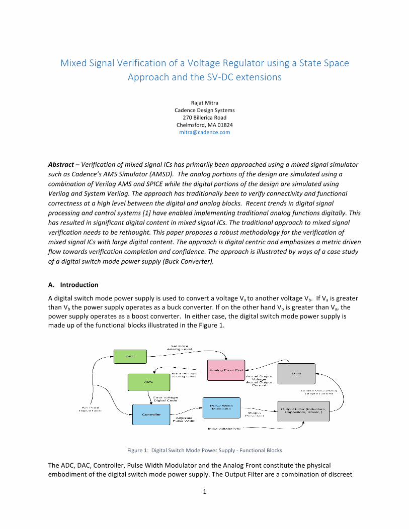
A digital switch mode power supply is used to convert a voltage Va to another voltage Vb. If Va is greater than Vb the power supply operates as a buck converter. If on the other hand Vb is greater than Va, the power supply operates as a boost converter. In either case, the digital switch mode power supply is made up of the functional blocks illustrated in the Figure 1.
Figure 1: Digital Switch Mode Power Supply -‐ Functional Blocks
The ADC, DAC, Controller, Pulse Width Modulator and the Analog Front constitute the physical embodiment of the digital switch mode power supply. The Output Filter are a combination of discreet

2
and active components that are driven by the digital switch mode power supply to produce an output voltage for the Load. The Load is time varying in terms of power consumption. This means that the current draw changes. When the current drawn by the load changes the output voltage will tend to droop or spike. The digital switch mode power supply detects these voltage changes and regulates the output voltage such that the droops and spikes are limited to a tolerance band. From a verification angle the methodology partitions the system into the following functional blocks – • The green blocks are representative of the analog/digital boundary. • The blue blocks are digital blocks (RTL). • The pink block is an analog block. • The grey blocks are board level components. The suggested approach has two verification contexts. The first is the metric driven flow where the green, blue, pink and grey blocks are replaced with functionally equivalent models. The second is the full chip functional flow where green and pink blocks are replaced with the real SPICE circuit. This paper details the first flow using the buck converter as an example. B. Functional Aspects of a Digital Switch Mode Power Supply In order to illustrate the verification aspects of a digital switch mode power supply it is instructive to outline the operational details of such an integrated circuit. This is done by analyzing each of the functional blocks of Figure 1. DAC The DAC or the Digital to Analog Converter takes a voltage command code from the user and converts it to an actual voltage level. The code to voltage conversion is dependent on the DAC’s resolution. The resolution is quoted is terms of a code step. For a 10-‐bit DAC which has a range from 0 to 1.5 volts, the resolution would be 1.5/210 or 1.46 millivolts per code step. DACs could also be specified in terms of a code step. Suppose a 10-‐bit DAC has a code step of 5 millivolts. Its range would be from 0 volts (assuming no built in offset) to 5.00e-‐3*210 or 5.12 volts. However when a DAC is specified this way an upper limit to the output voltage may be specified and this would restrict the available command codes(non-‐monotonic DAC). The example below illustrates a simple DAC model.
1. 2. `define DAC_RESOLUTION 5.00e-‐3 3. 4. module DAC(Y,A); 5. 6. input wire [9:0] A; 7. output real Y; 8. 9. assign Y = A*`DAC_RESOLUTION; 10. 11. 12. 13. endmodule
3
ADC The ADC or the Analog to Digital Converter samples a voltage and converts it to a digital code. The code to voltage conversion is dependent on the ADC’s resolution. The resolution is quoted in terms of a code step. A 10-‐bit ADC which has a range from 0 to 1.5 volts, would have a resolution of 1.5/210 or 1.46 millivolts per code step. ADCs could also be specified in terms of a code step. Suppose a 10 bit DAC has a code step of 5 millivolts. Its range would be from 0 volts (assuming no built in offset) to 5.00e-‐3*210 or 5.12 volts. Unlike a DAC, it is customary to clock an ADC. The example below illustrates a simple differential ADC model. The output of this ADC is a signed 7-‐Bit converted value. Later on it will be clear why the modeling requirements being discussed require a differential ADC.
1. module DIFF_ADC(input real vin, 2. output [6:0] conv 3. ); 4. 5. //Digitize the error voltage; sample and hold ADC 6. real vin_abs, vin_conv; 7. reg [6:0] conv; 8. bit vin_sgn; 9. 10. always begin 11. #10; //Sample period of 10ns 12. 13. vin_abs = vin < 0.00 ? -‐1.00*vin: vin; 14. vin_sgn = vin < 0.00 ? 1'b1 : 1'b0; 15. vin_conv = vin_abs; 16. conv_r = 0.000; 17. for(int ii=6; ii > -‐1; ii-‐-‐)begin 18. if(vin_conv > $pow(2,ii)*adc_resolution)begin 19. conv[ii] = 1'b1; 20. vin_conv = vin_conv -‐ $pow(2,ii)*adc_resolution; 21. end 22. else begin 23. conv[ii] = 1'b0; 24. end 25. end 26. //negate if the sampled voltage was negetive 27. conv = vin_sgn ? (~conv + 7'b1 ) : conv; 28. 29. //obtain real representation of converted value 30. //compare this with the actual sampled value -‐ DEBUG only 31. for(int ii=0; ii < 6; ii+=1)begin 32. conv_r = conv_r + conv[ii]*$pow(2,ii)*adc_resolution; 33. end 34. conv_r = conv_r -‐ conv[6]*$pow(2,6)*adc_resolution; 35. end // always @ (vin) 36. 37. endmodule // DIFF_ADC
Analog Front End (AFE) The analog end measures the voltage at the load and subtracts this from the commanded DAC voltage. The resulting voltage difference is the error voltage. The error voltage is what eventually is digitized by the ADC and forwarded to the controller. The controller acts on the error voltage to compensate for the under voltage (error voltage > 0 ) or the over voltage ( error voltage < 0 ) condition. Note the requirement for the differential ADC. The example below illustrates a simple AFE model.
4
1. module AFE(vin_m, vin_ref, v_delta); 2. 3. 4. input wreal vin_m; 5. input wreal vin_ref; 6. ouput wreal v_delta; 7. 8. 9. assign v_delta = vin_ref -‐ vin_m; 10. 11. 12. endmodule
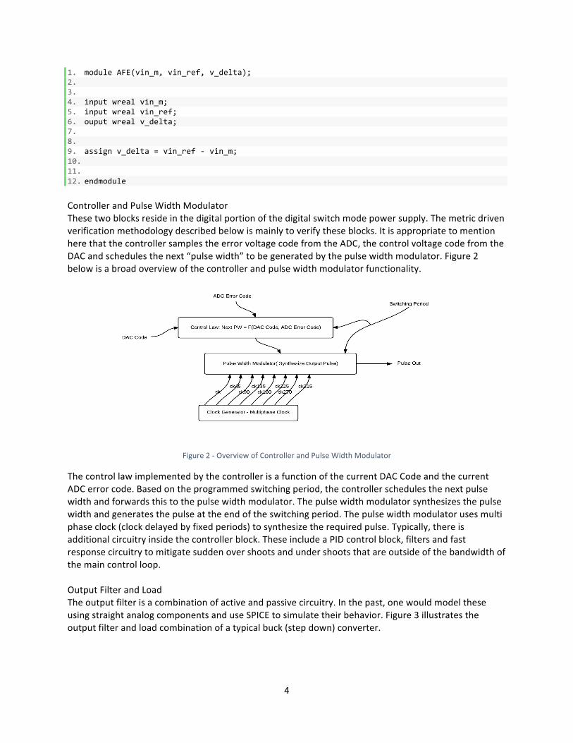
Controller and Pulse Width Modulator These two blocks reside in the digital portion of the digital switch mode power supply. The metric driven verification methodology described below is mainly to verify these blocks. It is appropriate to mention here that the controller samples the error voltage code from the ADC, the control voltage code from the DAC and schedules the next “pulse width” to be generated by the pulse width modulator. Figure 2 below is a broad overview of the controller and pulse width modulator functionality.
Figure 2 -‐ Overview of Controller and Pulse Width Modulator
The control law implemented by the controller is a function of the current DAC Code and the current ADC error code. Based on the programmed switching period, the controller schedules the next pulse width and forwards this to the pulse width modulator. The pulse width modulator synthesizes the pulse width and generates the pulse at the end of the switching period. The pulse width modulator uses multi phase clock (clock delayed by fixed periods) to synthesize the required pulse. Typically, there is additional circuitry inside the controller block. These include a PID control block, filters and fast response circuitry to mitigate sudden over shoots and under shoots that are outside of the bandwidth of the main control loop. Output Filter and Load The output filter is a combination of active and passive circuitry. In the past, one would model these using straight analog components and use SPICE to simulate their behavior. Figure 3 illustrates the output filter and load combination of a typical buck (step down) converter.

5
Figure 3 -‐ Buck Converter IC, Driver, FET, Output Filter and Load Assembly
The output driver and FETS can be modeled digitally using the following real number model.
1. import cds_rnm_pkg::*; 2. 3. module driver_and_FET(/*AUTOARG*/ 4. // Outputs 5. pwm_r, 6. // Inputs 7. pwm_d, vin 8. ); 9. 10. input wire pwm_d; 11. input vin; 12. output pwm_r; 13. 14. wreal1driver vin; 15. wreal1driver pwm_r; 16. 17. assign pwm_r = pwm_d ? vin : 0.00; 18. 19. endmodule // driver_and_FET
In what follows, a state space model of the output filter (load, resistors, capacitor and inductor) is combined with driver and FET to create a full digital metric driven verification environment for the digital voltage regulator. C. Methodology The next several sections will describe the requirements to create a full digital simulation environment. It is important that the verification effort is centered on an understanding of the functionality of the voltage regulator. A sound understanding of its functionality will help identify critical verification
6
requirements. This will be discussed in section 1. The state space approach to modeling the output filter is discussed in Section 2. The paper also explains how the SV-‐DC extensions to System Verilog 1800-‐2012 is used in conjunction with the state space approach to create a highly effective metric driven mixed signal test bench. This along with several new features to constrain randomize real numbers will be the subject of Section 3.
1. The Buck Converter There is ample literature [2], [3], [4] that detail the functionality of a buck converter. In this section, we will outline the pertinent aspects of such a device that is important for the verification effort. In what follows, details of the controller and the pulse width modulator are explained. The controller implements a control law. The control law for a buck converter is the–
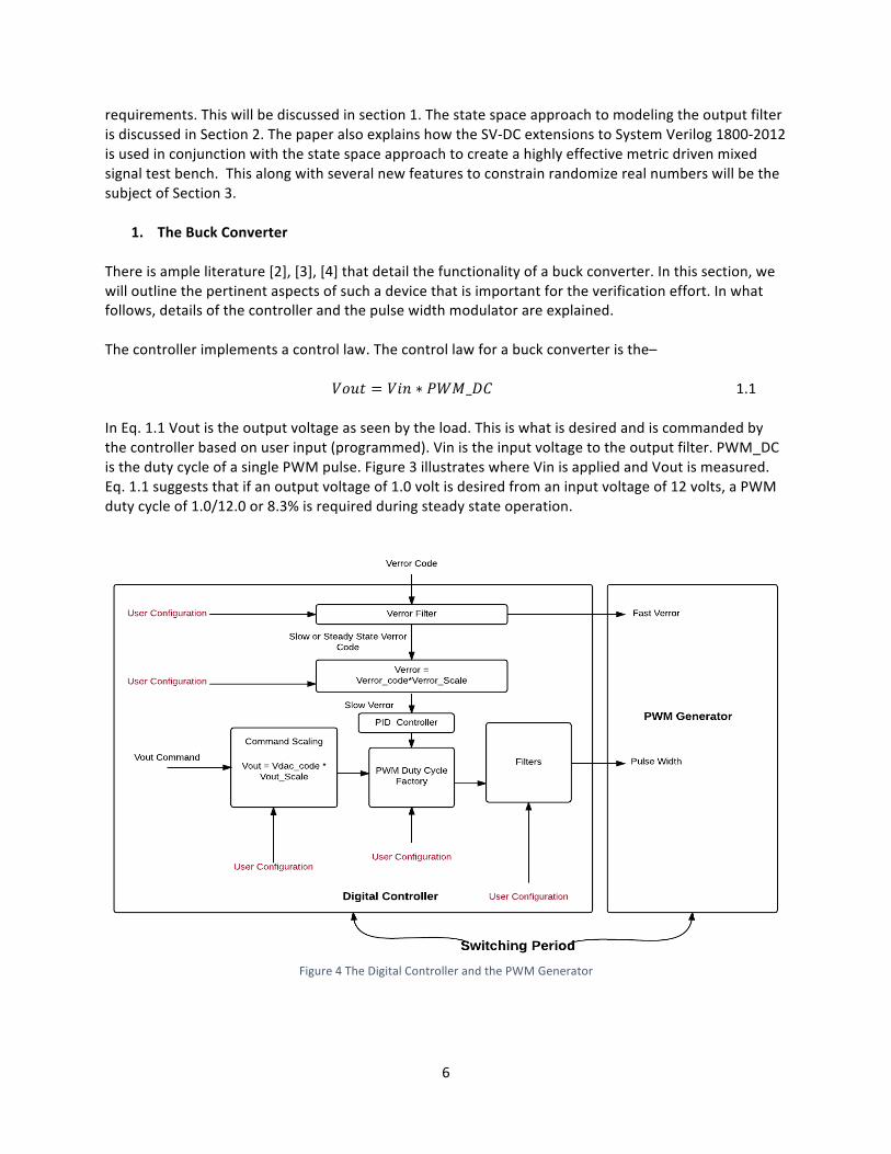
𝑉𝑜𝑢𝑡 = 𝑉𝑖𝑛 ∗ 𝑃𝑊𝑀_𝐷𝐶 1.1 In Eq. 1.1 Vout is the output voltage as seen by the load. This is what is desired and is commanded by the controller based on user input (programmed). Vin is the input voltage to the output filter. PWM_DC is the duty cycle of a single PWM pulse. Figure 3 illustrates where Vin is applied and Vout is measured. Eq. 1.1 suggests that if an output voltage of 1.0 volt is desired from an input voltage of 12 volts, a PWM duty cycle of 1.0/12.0 or 8.3% is required during steady state operation.
Figure 4 The Digital Controller and the PWM Generator
7
Were the controller to operate as open loop systems, implementation of equation 1.1 would be fairly straightforward. However this is rarely the case. The controller in reality is feedback based. Figure 4 illustrates the functional aspects of the controller.
The Analog Front End (AFE) illustrated in Figure 1 creates the voltage difference between the desired or commanded voltage and the voltage measured at the load. This voltage difference is the error voltage. The high-‐speed differential ADC digitizes the error voltage (Verror Code). Note that the ADC has to be differential since the error can be positive or negative. The error is positive if the commanded voltage is greater than the measured output voltage. The error is negative if the commanded voltage is lower than the measured output voltage. This can be seen from the AFE model code presented above. The error voltage is sent to a filter block (Verror Filter). The filter block smoothens the error information through the low bandwidth path for steady state operation. A higher bandwidth path through this block creates wider band error information for the PWM generator to act on during sudden voltage transients. The slow voltage error is finally processed through a PID controller. The PID controller attempts to force the error voltage to zero.
The command-‐scaling block receives an output voltage command from the user and arithmetically scales the command code as depicted in Figure 4. Pre-‐scaling the command code and the error code to a common arithmetic format is efficient for subsequent processing. In the design specification it is important to identify the arithmetic format for every I/O in the major block in the controller. For instance one might state that the Vout signal’s format is u1.5. This would mean that the signal is unsigned, has one integer bit and 5 fractional bits. The Slow Verror and the Vout data are fed to the PWM duty cycle factory. The PWM Duty Cycle Factory uses the Slow Verror and the Vout information to stage the duty cycle of the next modulator pulse. One might implement the equation for the next modulator pulse as follows –
𝑃𝑢𝑙𝑠𝑒 𝑊𝑖𝑑𝑡ℎ =𝑉𝑜𝑢𝑡 + 𝑉𝑒𝑟𝑟𝑜𝑟
𝑉𝑖𝑛
1.2
The proper implementation and verification of 1.2 is challenging. As previously mentioned, Vout and Verror need to have the same arithmetic format. Scaling procedures to unify their format can be expensive from a hardware point-‐on-‐view and error prone. The divide by Vin might be implemented assuming a constant Vin. In this case, the reciprocal of Vin is pre-‐computed and the resultant is scaled to have a consistent format so that equation 1.2 might be recast as –
𝑃𝑢𝑙𝑠𝑒 𝑊𝑖𝑑𝑡ℎ = 𝑉𝑜𝑢𝑡 + 𝑉𝑒𝑟𝑟𝑜𝑟 ∗ 𝐼𝑛𝑣𝑒𝑟𝑠𝑒_𝑜𝑓(𝑉𝑖𝑛) 1.3
However this is rarely the case and the implementation in 1.2 is the one of choice. This is because variations in Vin need to be tracked. Vin is measured by a low bandwidth ADC and sent to the digital controller. The divider might be implemented in several different ways but the fastest way to do so is by using the Newton-‐Raphson algorithm [5]. Others such as SRT, restoring and non-‐restoring division [6] are also common. In the Newton-‐Raphson method, the reciprocal of Vin is determined. This reciprocal is

8
used to scale Vout + Verror. Each divide might take several cycles and consequently the sudden variations in Vin might not be effected instantaneously. This posses a verification challenge.
The pulse width value computed by the digital control block is filtered and sent to the PWM generator. This information is used to synthesize the output pulse based on the specified switching period. The switching period is the time between two consecutive rising edges of the output pulse train and is configured by the user. An example of output pulse synthesis by the modulator is illustrated in Figure 5.
Figure 5 -‐ Multi Phase Clock Pulse Synthesis
Figure 5 shows an example of how the multi phase clocks are logically OR-‐ed to create a single pulse. If the pulse width is specified in terms of the number of multi phase clock periods the PWM Generator will divide this number by 8 (since in this implementation there are 8 multi phase clocks) to create an integral(quotient) and fractional(remainder) pulse count. For the first phase of the output pulse, all the multi phase clocks are OR-‐ed for an integral count of the clock period. When the integral count is exhausted, the remaining fractional count is implemented in a single clock period and this is the OR-‐ing of the remaining multi phase clock pulses.
The PWM generator implementation stated above is one of several. Clearly the higher the multi phase clock resolution(say 16 as opposed to 8), the more accurately the output voltage may be regulated.
2. The State Space Approach to Modeling the Output Filter
The state space method is popular in modeling control system behavior. There is ample literature that derives and explains this technique [7]. This section will briefly outline the state space methodology and use it to derive the equations for the output filter. This equation and the model equations for the driver and FET will be discussed in context of the simulation environment.
A means to model a dynamical system is to identify observable properties of that system. These properties are quantified mathematically in terms of a variable. Examples include the velocity of a

9
moving vehicle, the temperature of a heating element, the current through an inductor and the voltage across a capacitor. If the state of a system can be characterized by these variables then the variables are termed state variables for the system. An important property of these variables is that if their state is known at any given time (current state) along with the agents that influence their value (the inputs to the system), then it is possible to measure the behavior of the systems state variables at any future time (the output of the system).
In electrical engineering, one broadly speaks of two types of systems. A digital system is classified as a discreet time system. An analog system is classified as a continuous time system. Let x(t) be a continuous time state variable. This variable can be interpreted as the value of property “x” of a systems at time “t”. The property could be voltage or current. Using the state space approach a closed form equation for the rate of change of x(t) can be written as follows –
𝑑𝑥 𝑡𝑑𝑡
= 𝐴𝑥 𝑡 + 𝐵𝑢(𝑡) 2.1
This equation says that the rate of change of x(t) depends on the current value of x(t) and the applied input u(t). Coefficients A and B are determined based on physical laws that relate the current state and the applied input to the rate change of the state variable. In the case of the output filter these are derived from Kirchhoff’s Laws as will be shown shortly.
In passing it is instructive to mention the equivalent equation to 3.1 for a digital system is written as follows –
𝑥 𝑛 + 1 = 𝐴′𝑥 𝑛 + 𝐵′𝑢(𝑛) 2.2
where “n” replaces the time variable as the n-‐th sampled value of “x” and “u”.
To derive the equations for the output filter consider the representative circuitry illustrated in Figure 6. The output capacitors are modeled as a single equivalent capacitor C with equivalent series resistor E_ESR. The inductor L is included with its DC resistance as R_DCR. The PWM pulses are modeled as a voltage source V_PULSE. The output load is modeled using a controlled current source I_LOAD.
Figure 6 -‐ Simple Output Filter (Powertrain) and Load (approximation of Figure 3)

10
Using Kirchhoff’s laws we can write down the following equations for this circuit –
𝑑𝑖!𝑑𝑡
= −𝑅!"# + 𝑅!"#
𝐿∗ 𝑖! −
1𝐿∗ 𝑣! −
𝑅!"#𝐿
∗ 𝐼!"#$ +1𝐿∗ 𝑉!"#$%
2.3
𝑑𝑣!𝑑𝑡
=1𝐶∗ 𝑖! + 0 ∗ 𝑣! −
1𝐶∗ 𝐼!"#$ + 0 ∗ 𝑉!"#$%
2.4
2.3 and 2.4 are equations that express the current through the inductor and the voltage across the output capacitor. The output driver and FETS are absorbed into voltage source (a reasonable approximation). The approximations made are extremely effective in simulating the digital controller behavior. Knowing the rate of change of these two key state variables (voltage across the capacitor and the current through the inductor) it is possible to create a simulation model of the output filter. Choose a simulation timestep ‘dt’. It can then be shown –
𝑖! 𝑡 + 𝑑𝑡 = 𝑖! 𝑡 + 𝑑𝑡 ∗ 𝐹(!!!!") 2.5
𝑣! 𝑡 + 𝑑𝑡 = 𝑣! 𝑡 + 𝑑𝑡 ∗ 𝐹(!!! !") 2.6
Here F() and G() are functions of the rate of change of iL and vc. They can be chosen in several different ways. Two that are popular are the Runge-‐Kutta and the Forward Euler approximations[8]. The Forward Euler approximation will be used to demonstrate the modeling approach.
Consider a function y(t) around t0 . The Taylor expansion of y(t) around t0 can be written as –
𝑦 𝑡! + 𝑑𝑡 = 𝑦 𝑡! + 𝑑𝑡 ∗𝑑𝑦 𝑡!𝑑𝑡
+12∗ 𝑑𝑡! ∗
𝑑!𝑦 𝑡!𝑑𝑡
+ 𝑂(𝑑𝑡!) 2.7
This equation assumes that the derivatives and higher order derivatives of y(t) exist around t0 . The Euler approximation to 2.7 assumes that terms of higher orders than one (of dt) are small enough to be ignored. As smaller time steps are chosen the accuracy of the Euler approximation increases. Having stated the definition of the Euler approximation equations 2.5 and 2.6 can be recast as follows –
𝑖! 𝑡 + 𝑑𝑡 = 𝑖! 𝑡 + 𝑑𝑡 ∗𝑑𝑖!(𝑡)𝑑𝑡
2.8
𝑣! 𝑡 + 𝑑𝑡 = 𝑣!(𝑡) + 𝑑𝑡 ∗𝑑𝑣!(𝑡)𝑑𝑡
2.9
where diL/dt and dvc /dt are as defined in equations 2.3 and 2.4. The reader is encouraged to
11
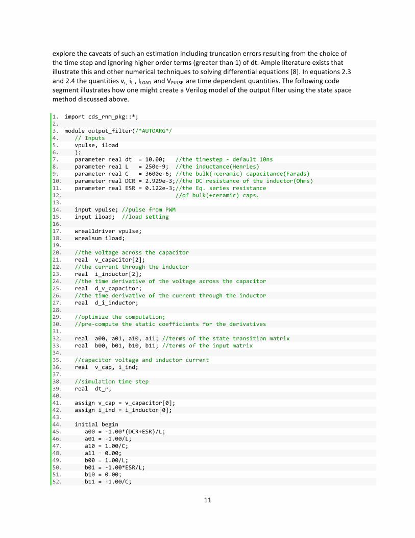
explore the caveats of such an estimation including truncation errors resulting from the choice of the time step and ignoring higher order terms (greater than 1) of dt. Ample literature exists that illustrate this and other numerical techniques to solving differential equations [8]. In equations 2.3 and 2.4 the quantities vc, iL , ILOAD and VPULSE are time dependent quantities. The following code segment illustrates how one might create a Verilog model of the output filter using the state space method discussed above.
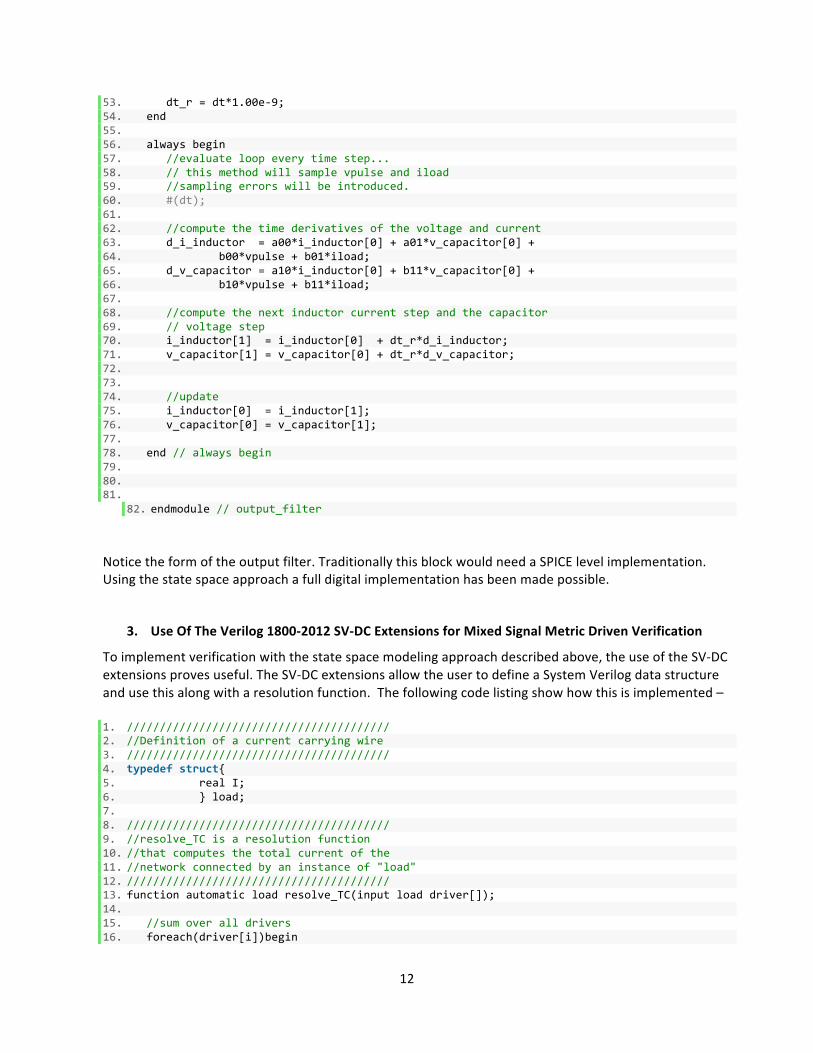
1. import cds_rnm_pkg::*; 2. 3. module output_filter(/*AUTOARG*/ 4. // Inputs 5. vpulse, iload 6. ); 7. parameter real dt = 10.00; //the timestep -‐ default 10ns 8. parameter real L = 250e-‐9; //the inductance(Henries) 9. parameter real C = 3600e-‐6; //the bulk(+ceramic) capacitance(Farads) 10. parameter real DCR = 2.929e-‐3;//the DC resistance of the inductor(Ohms) 11. parameter real ESR = 0.122e-‐3;//the Eq. series resistance 12. //of bulk(+ceramic) caps. 13. 14. input vpulse; //pulse from PWM 15. input iload; //load setting 16. 17. wreal1driver vpulse; 18. wrealsum iload; 19. 20. //the voltage across the capacitor 21. real v_capacitor[2]; 22. //the current through the inductor 23. real i_inductor[2]; 24. //the time derivative of the voltage across the capacitor 25. real d_v_capacitor; 26. //the time derivative of the current through the inductor 27. real d_i_inductor; 28. 29. //optimize the computation; 30. //pre-‐compute the static coefficients for the derivatives 31. 32. real a00, a01, a10, a11; //terms of the state transition matrix 33. real b00, b01, b10, b11; //terms of the input matrix 34. 35. //capacitor voltage and inductor current 36. real v_cap, i_ind; 37. 38. //simulation time step 39. real dt_r; 40. 41. assign v_cap = v_capacitor[0]; 42. assign i_ind = i_inductor[0]; 43. 44. initial begin 45. a00 = -‐1.00*(DCR+ESR)/L; 46. a01 = -‐1.00/L; 47. a10 = 1.00/C; 48. a11 = 0.00; 49. b00 = 1.00/L; 50. b01 = -‐1.00*ESR/L; 51. b10 = 0.00; 52. b11 = -‐1.00/C;
12
53. dt_r = dt*1.00e-‐9; 54. end 55. 56. always begin 57. //evaluate loop every time step... 58. // this method will sample vpulse and iload 59. //sampling errors will be introduced. 60. #(dt); 61. 62. //compute the time derivatives of the voltage and current 63. d_i_inductor = a00*i_inductor[0] + a01*v_capacitor[0] + 64. b00*vpulse + b01*iload; 65. d_v_capacitor = a10*i_inductor[0] + b11*v_capacitor[0] + 66. b10*vpulse + b11*iload; 67. 68. //compute the next inductor current step and the capacitor 69. // voltage step 70. i_inductor[1] = i_inductor[0] + dt_r*d_i_inductor; 71. v_capacitor[1] = v_capacitor[0] + dt_r*d_v_capacitor; 72. 73. 74. //update 75. i_inductor[0] = i_inductor[1]; 76. v_capacitor[0] = v_capacitor[1]; 77. 78. end // always begin 79. 80. 81.
82. endmodule // output_filter
Notice the form of the output filter. Traditionally this block would need a SPICE level implementation. Using the state space approach a full digital implementation has been made possible.
3. Use Of The Verilog 1800-‐2012 SV-‐DC Extensions for Mixed Signal Metric Driven Verification
To implement verification with the state space modeling approach described above, the use of the SV-‐DC extensions proves useful. The SV-‐DC extensions allow the user to define a System Verilog data structure and use this along with a resolution function. The following code listing show how this is implemented –
1. //////////////////////////////////////// 2. //Definition of a current carrying wire 3. //////////////////////////////////////// 4. typedef struct{ 5. real I; 6. } load; 7. 8. //////////////////////////////////////// 9. //resolve_TC is a resolution function 10. //that computes the total current of the 11. //network connected by an instance of "load" 12. //////////////////////////////////////// 13. function automatic load resolve_TC(input load driver[]); 14. 15. //sum over all drivers 16. foreach(driver[i])begin
13
17. resolve_TC.I += driver[i].load; 18. end 19. 20. endfunction
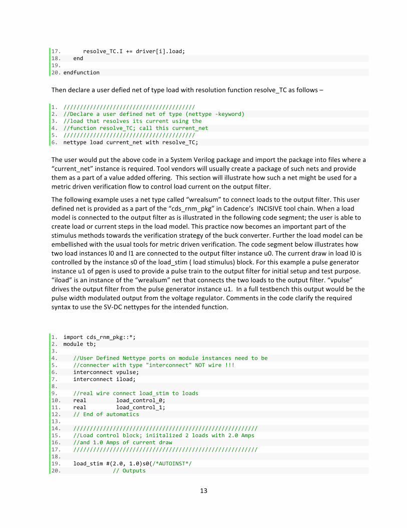
Then declare a user defied net of type load with resolution function resolve_TC as follows –
1. //////////////////////////////////////// 2. //Declare a user defined net of type (nettype -‐keyword) 3. //load that resolves its current using the 4. //function resolve_TC; call this current_net 5. //////////////////////////////////////// 6. nettype load current_net with resolve_TC;
The user would put the above code in a System Verilog package and import the package into files where a “current_net” instance is required. Tool vendors will usually create a package of such nets and provide them as a part of a value added offering. This section will illustrate how such a net might be used for a metric driven verification flow to control load current on the output filter.
The following example uses a net type called “wrealsum” to connect loads to the output filter. This user defined net is provided as a part of the “cds_rnm_pkg” in Cadence’s INCISIVE tool chain. When a load model is connected to the output filter as is illustrated in the following code segment; the user is able to create load or current steps in the load model. This practice now becomes an important part of the stimulus methods towards the verification strategy of the buck converter. Further the load model can be embellished with the usual tools for metric driven verification. The code segment below illustrates how two load instances l0 and l1 are connected to the output filter instance u0. The current draw in load l0 is controlled by the instance s0 of the load_stim ( load stimulus) block. For this example a pulse generator instance u1 of pgen is used to provide a pulse train to the output filter for initial setup and test purpose. “iload” is an instance of the “wrealsum” net that connects the two loads to the output filter. “vpulse” drives the output filter from the pulse generator instance u1. In a full testbench this output would be the pulse width modulated output from the voltage regulator. Comments in the code clarify the required syntax to use the SV-‐DC nettypes for the intended function.
1. import cds_rnm_pkg::*; 2. module tb; 3. 4. //User Defined Nettype ports on module instances need to be 5. //connecter with type "interconnect" NOT wire !!! 6. interconnect vpulse; 7. interconnect iload; 8. 9. //real wire connect load_stim to loads 10. real load_control_0; 11. real load_control_1; 12. // End of automatics 13. 14. //////////////////////////////////////////////////////// 15. //Load control block; iniitalized 2 loads with 2.0 Amps 16. //and 1.0 Amps of current draw 17. //////////////////////////////////////////////////////// 18. 19. load_stim #(2.0, 1.0)s0(/*AUTOINST*/ 20. // Outputs
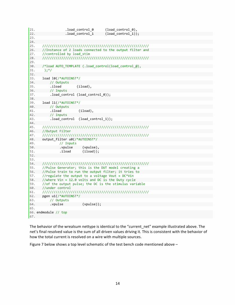
14
21. .load_control_0 (load_control_0), 22. .load_control_1 (load_control_1)); 23. 24. 25. //////////////////////////////////////////////////////// 26. //Instance of 2 loads connected to the output filter and 27. //controlled by load_stim 28. //////////////////////////////////////////////////////// 29. 30. /*load AUTO_TEMPLATE (.load_control(load_control_@), 31. );*/ 32. 33. load l0(/*AUTOINST*/ 34. // Outputs 35. .iload (iload), 36. // Inputs 37. .load_control (load_control_0)); 38. 39. load l1(/*AUTOINST*/ 40. // Outputs 41. .iload (iload), 42. // Inputs 43. .load_control (load_control_1)); 44. 45. //////////////////////////////////////////////////////// 46. //Output Filter 47. //////////////////////////////////////////////////////// 48. output_filter u0(/*AUTOINST*/ 49. // Inputs 50. .vpulse (vpulse), 51. .iload (iload)); 52. 53. 54. //////////////////////////////////////////////////////// 55. //Pulse Generator; this is the DUT model creating a 56. //Pulse train to run the output filter; it tries to 57. //regulate the output to a voltage Vout = DC*Vin 58. //where Vin = 12.0 volts and DC is the Duty cycle 59. //of the output pulse; the DC is the stimulus variable 60. //under control 61. //////////////////////////////////////////////////////// 62. pgen u1(/*AUTOINST*/ 63. // Outputs 64. .vpulse (vpulse)); 65. 66. endmodule // top 67.
The behavior of the wrealsum nettype is identical to the “current_net” example illustrated above. The net’s final resolved value is the sum of all driven values driving it. This is consistent with the behavior of how the total current is resolved on a wire with multiple sources.
Figure 7 below shows a top level schematic of the test bench code mentioned above –
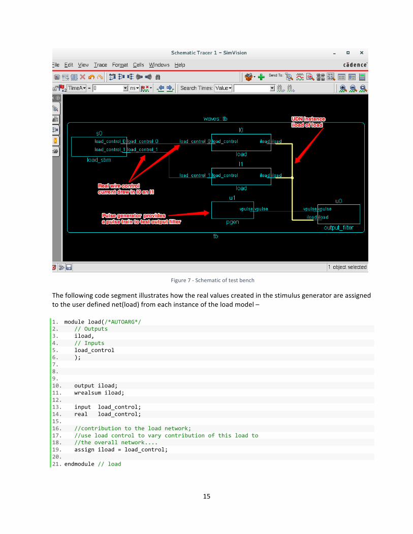
15
Figure 7 -‐ Schematic of test bench
The following code segment illustrates how the real values created in the stimulus generator are assigned to the user defined net(load) from each instance of the load model –
1. module load(/*AUTOARG*/ 2. // Outputs 3. iload, 4. // Inputs 5. load_control 6. ); 7. 8. 9. 10. output iload; 11. wrealsum iload; 12. 13. input load_control; 14. real load_control; 15. 16. //contribution to the load network; 17. //use load control to vary contribution of this load to 18. //the overall network.... 19. assign iload = load_control; 20. 21. endmodule // load

16
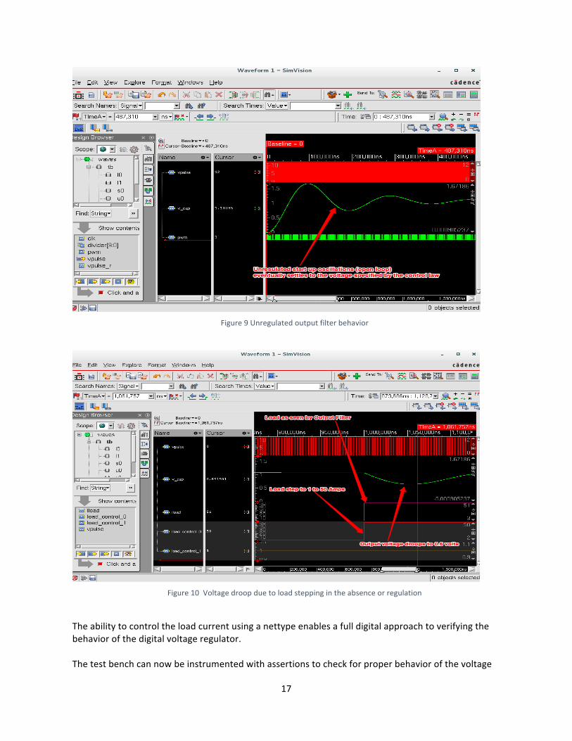
In the mentioned testbench a pulse generator is used to demonstrate the functionality of the output filter. Figure 8 illustrates a voltage output from the output filter when the pulse generator creates an output pulse at 9.0% duty cycle. The input voltage is 12 volts. From 1.1 the output voltage or the voltage on the output capacitor of the output filter should approximately be 1.08 volt. This is evident in the figure during steady state operation –
Figure 8 Vpulse vs Output Voltage
Since the pulse generator is not regulating the output voltage and the output filter is under damped, one might expect a lot of overshoot and undershoot during startup. This is indeed the case as is illustrated in Figure 9.
The load (current) stepping behavior is demonstrated by varying the current in either loads from the load_stim instance of the stimulus generator. Figure 10 illustrates the output voltage undershoot when load instance l0 goes from 2 amps to 50 amps and load 1 remains at 1 amp. iload which is the total current load as seen by the output filter goes from 3 amps to 51 amps. This will cause the output voltage to droop all the way down to 0.6 volts. This is undesired but unavoidable without regulation. Figure 10 depicts the load stepping behavior.
17
Figure 9 Unregulated output filter behavior
Figure 10 Voltage droop due to load stepping in the absence or regulation
The ability to control the load current using a nettype enables a full digital approach to verifying the behavior of the digital voltage regulator. The test bench can now be instrumented with assertions to check for proper behavior of the voltage
18
regulator. Common checks that are critical to implement in a test bench to guarantee safe operation of the voltage regulator include –
• Check for over voltage behavior; occurs during load release. • Check for under voltage behavior; occurs during load stepping. • Check for over current behavior; occurs during load stepping, might even occur during load
release. • Check over voltage fault; usually when this condition is created by the stimulus and the regulator
is unable to mitigate through regulation, the regulator is expected to shutdown. • Check under voltage fault; same explanation as over voltage fault. • Check over current fault; here the test bench generates a stimulus to step the load beyond the
maximum output load programmed in the voltage regulator. The regulator is expected to shutdown.
The following lists a set of assertions that check for these behavior –
1. ////////////////////////////////////////////////////// 2. //Properties 3. ////////////////////////////////////////////////////// 4. 5. //Property to make sure voltage overshoots are within bounds 6. property voltage_bound_max; 7. @(posedge clk) 8. disable iff(~(enable && in_ss_regulation)) 9. voltage < regulation_voltage + max_voltage_overshoot; 10. endproperty 11. 12. //Property to make sure voltage undershoots are within bounds 13. property voltage_bound_min; 14. @(posedge clk) 15. disable iff(~(enable && in_ss_regulation)) 16. voltage > regulation_voltage -‐ min_voltage_droop; 17. endproperty 18. 19. //Property to make sure current overshoots are within bounds 20. property current_bound_max; 21. @(posedge clk) 22. disable iff(~(enable && in_ss_regulation)) 23. current < max_current_overshoot; 24. endproperty 25. 26. //Property to check voltage slew is below max bound 27. property voltage_slew_max_bound; 28. @(posedge clk) 29. disable iff(-‐(enable && in_voltage_transition)) 30. voltage_slew < max_voltage_slew; 31. endproperty 32. 33. 34. //Property to check voltage slew is above min bound 35. property voltage_slew_min_bound; 36. @(posedge clk) 37. disable iff(-‐(enable && in_voltage_transition)) 38. voltage_slew > min_voltage_slew; 39. endproperty 40.
19
41. //Property to chcek over voltage condition and subsequent chip shutdown 42. property shutdown_ov; 43. @(posedge clk) 44. detect_voltage_high |-‐>~(in_ss_regulation | in_voltage_transition ); 45. endproperty 46. 47. //Property to chcek under voltage condition and subsequent chip shutdown 48. property shutdown_uv; 49. @(posedge clk) 50. detect_voltage_low |-‐>~(in_ss_regulation | in_voltage_transition ); 51. endproperty 52. 53. //Property to chcek over current condition and subsequent chip shutdown 54. property shutdown_oc; 55. @(posedge clk) 56. detect_current_high |-‐>~(in_ss_regulation | in_voltage_transition ); 57. endproperty 58. 59. //Property to check over voltage condition 60. sequence detect_voltage_high; 61. voltage > regulation_voltage + max_voltage_overshoot ##(fault_response_ov) 62. voltage_hi_fault; 63. endsequence // detect_voltage_high 64. 65. //property to check under voltage condition 66. sequence detect_voltage_low; 67. voltage < regulation_voltage -‐
min_voltage_droop ##(fault_response_uv) voltage_lo_fault; 68. endsequence // detect_voltage_low 69. 70. //property to check over current condition 71. sequence detect_current_high; 72. current > max_current_overshoot ##(fault_response_oc) current_hi_fault; 73. endsequence // detect_current_high 74.
The above variables are defined as follows –
1. program asserts_real(/*AUTOARG*/ 2. // Inputs 3. voltage, regulation_voltage, current, clk, enable, 4. in_ss_regulation, in_voltage_transition, voltage_hi_fault, 5. voltage_lo_fault, current_hi_fault 6. ); 7. 8. parameter real min_voltage_droop = 0.5; //Powertrain Minimum Voltage Droop 9. //(Volts V) 10. parameter real max_voltage_overshoot = 1.5; //Powertrain Maximum Voltage Overshoot 11. //(Volts V) 12. parameter real max_current_overshoot = 50.00;//Powertrain Maximum Current Overshoot 13. //(Ampere A) 14. parameter real max_voltage_slew = 5.00e3; //Powertrain Maximum Voltage Slew 15. //(Volts/usec) 16. parameter real min_voltage_slew = 10.00e3; //Powertrain Minimum Voltage Slew 17. //(Volts/usec) 18. parameter int fault_response_ov = 100; //DUT Over Voltage Fault Response Time 19. //(nsec) 20. parameter int fault_response_uv = 100; //DUT Under Voltage Fault Response Time 21. //(nsec) 22. parameter int fault_response_oc = 100; //DUT Over Current Fault Response Time
20
23. //(nsec) 24. parameter int sampling_period = 1000; //Voltage Sampling Period 25. //(nsec) 26. 27. 28. input real voltage; //Instantaneous Output Voltage 29. input real regulation_voltage; //Commanded Voltage 30. input real current; //Instantaneous Output Current 31. input logic clk; //Sampling Clock 32. input logic enable; //Chip Enable 33. input logic in_ss_regulation; //Steady State Regulation Flag 34. input logic in_voltage_transition; //Voltage Transitioning Flag 35. input logic voltage_hi_fault; //Detect Over Voltage Flag 36. input logic voltage_lo_fault; //Detect Under Voltage Flag 37. input logic current_hi_fault; //Detect Over Current Falg
Once these assertion based checks are implemented, it now becomes crucial to implement the proper stimulus so that all checks are covered. Typically in a digital voltage regulator, the control loop and fault management circuitry are programmed with performance and functional parameters respectively. The fault management circuitry is programed with over voltage, under voltage and over current limits. The control parameter from the test bench side for the implementation described here is the load. The manner in which the load is stepped (up and down) influences the response of the control loop (this includes the model of the output filter described previously). The load control is implemented using a load management class structure. This is illustrated in the code segment below –
1. /////////////////////////////////////////////////////// 2. //Load Control Package 3. /////////////////////////////////////////////////////// 4. package load_control_pkg; 5. 6. //Load Management Class 7. class load_manage; 8. 9. virtual load_intf.DRIVER load_cntl; 10. 11. function new(virtual load_intf.DRIVER load_cntl); 12. this.load_cntl = load_cntl; 13. load_cntl.val = 0.00; 14. endfunction // new 15. 16. //////////////////////////////////////////////////// 17. //User controlled Load Ramp(Ramp Up and Down) 18. //////////////////////////////////////////////////// 19. task ramp_load_up(real value, int steps, int period); 20. 21. for(int ii=0; ii < steps; ii++)begin 22. load_cntl.val = load_cntl.val + value/steps; 23. $display("INFO:Ramp Load Up at time %t..",$time); 24. #(period);

21
25. end 26. 27. endtask // ramp_load_up 28. 29. task ramp_load_down(real value, int steps, int period); 30. 31. for(int ii=0; ii < steps; ii++)begin 32. load_cntl.val = load_cntl.val -‐ value/steps; 33. #(period); 34. end 35. 36. endtask // ramp_load_down 37. 38. endclass // load_manage 39. 40. endpackage // load_control
A simple interface connects this class to the output filter and this interface is illustrated below –
1. //////////////////////////////////////////////////////// 2. //Load Interface 3. ///////////////////////////////////////////////////////// 4. interface load_intf; 5. 6. wreal1driver wload; 7. real val; 8. assign wload = val; 9. 10. modport DRIVER(output val); 11. modport RECVR(input wload); 12. 13. 14. endinterface // load_intf
So far the discussion was centered on testbench control of the load stimulus. The other important control parameter of interest is the commanded voltage. Figure 11 illustrates a real regulator being commanded to several voltage points (the pulse generator was removed and the actual regulator was put in its place) in this testbench. The dac_reference is what is commanded by the digital interface. In this case the commanded voltage is in the form of a DAC code that is written to a voltage command register by the testbench. When a new command code is received the regulator ramps up or down to the commanded voltage. The waveforms in Figure 11 also show what happens to the output current when the output voltage is in transition. Without proper regulation the output current could potentially exceed the current limit programmed in the fault management logic and cause the regulator to shutdown (if the fault management logic works properly) or continue to operate and cause a system failure (if the fault management logic fails to detect the over current condition).
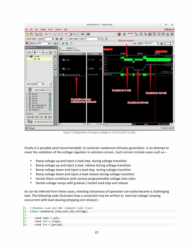
22
Figure 11 Regulation of output voltage to 1.0, 0.5 and 1.5 volts
Finally it is possible (and recommended) to constrain randomize stimulus generation in an attempt to cover the validation of the voltage regulator in extreme corners. Such corners include cases such as –
• Ramp voltage up and inject a load step during voltage transition • Ramp voltage up and inject a load release during voltage transition • Ramp voltage down and inject a load step during voltage transition • Ramp voltage down and inject a load release during voltage transition • Iterate these conditions with various programmable voltage slew rates • Iterate voltage ramps with gradual / instant load step and release
As can be inferred from these cases, checking robustness of operation can easily become a challenging task. The following code illustrates how a constraint may be written to exercise voltage ramping concurrent with load slewing (stepping ore release) –
1. //Random Load and DAC Command Code Class 2. class randomize_load_and_cmd_voltage; 3. 4. rand real r_val; 5. rand int r_steps; 6. rand int r_period;
23
7. rand int r_dac_code; 8. 9. constraint val_constraint {r_val >=10.00; r_val < 20.00;} 10. constraint steps_constraint {r_steps >=0; r_steps < 100;} 11. constraint period_constriant {r_period >= 100; r_period < 1000;} 12. constraint dac_code_constraint {r_dac_code >=50; r_dac_code < 200;} 13. 14. endclass // randomize_load
This class would be randomized and passed to the transaction object in the testbench which would stimulate the load and command voltage code concurrently. This transaction object can be equipped with covergroups to track coverage information. D. Conclusion This paper attempted to introduce the reader to a viable methodology for mixed signal verification. Extending this approach with more verification centric objectives (particularly incorporating UVM) will make it suitable for a rigorous digital centric mixed single testbenches. This work continues. A UVM library is being crafted around this methodology and the author seeks reader inputs towards this effort. It must be emphasized that the suggested approach is targeted with two goals in mind –
• A modeling and design goal – In such a case, the analog and mixed signal models / environment would be used as tools towards designing the controller by the designer.
• A full digital metric driven verification goal – As was discussed. It is important to bear in mind that the suggested approach is not a substitute for full chip simulation with the real analog circuitry. Only a full chip simulation with the correct SPICE circuitry will guarantee proper connectivity between the analog and digital domains. What is possible with this method is identification of operational corner (in linear operational mode) cases and making sure that the DUT handles these cases correctly. A properly crafted testbench will allow easy substitution of the analog /mixed signal models with their SPICE counterpart and this seamless substitution technology exists today. While this approach centers around a case study of a voltage regulator, it should be evident that it is applicable for any kind of control loop simulation and verification. Finally it should be emphasized that voltage regulators operate in extreme environments where the operational behavior becomes non-‐linear. What has been presented is a vista into the realm of possibilities of verifying control systems using a full digital approach. Work continues to extend this approach to model non-‐linear behavior. The authors welcomes ideas that the reader may have. E. Acknowledgements The authors would like to extend his sincerest thanks to colleagues at Cadence Design Systems. Aaron Spratt, Michael DeLanzo and Shekar Chetput took the time to review this paper and provide useful feedback. This paper would not have been possible without encouragement from Umer Yousefzai, Adam Sherer, Mladen Nizic and Hao Fang. Many thanks go to Venkat Sreenivas at Infineon Technologies who nurtured the author’s interest in the area of digital control theory. Finally thanks to Michael Quadri from Intel for providing insightful feedback.
24
F. References [1] http://www.irf.com/product/_/N~1nje1g [2] Christophe Basso, “Designing Switch-‐Mode Power Supplies – SPICE Simulations and Practical Practical Design”, McGraw-‐Hill Inc., 2008 [3] Christophe Basso, “Designing Control Loops for Linear and Switching Power Supplies: A Tutorial Guide”, Artech House, 2012 [4] Abraham I. Pressman, et al, “Switching Power Supply Design”, Third Edition, McGraw-‐Hill Inc.,2009 [5],[6] Israel Koren, “Computer Arithmetic Algorithms”, A.K Peters Ltd., Second Edition, 2001 [7] Katshuiko Ogata, “Modern Control Engineering”, Prentice Hall, Fifth Edition, 2010 [9] Steven Chapra, et al, “Numerical Methods for Engineers”, McGraw-‐Hill Inc., Sixth Edition, 2010