mlx91219 - mel-prd-cdn.azureedge.net
TRANSCRIPT

MLX91219 High Speed High Accuracy Current Sensor IC with dual OCD Datasheet
Features and Benefits ▪ End-of-line programmable sensor
▪ Factory selected 5V or 3.3V supply
▪ Measurement range from ±12 to ±500mT
▪ High speed AC and DC current sensing
▪ 400kHz bandwidth
▪ 2μs response time
▪ High linearity down to ±0.5% full scale
▪ Low noise
▪ AEC-Q100 – Grade 0 Automotive Qualification
▪ Very low thermal drift for wide range
▪ Offset drift (<5mV)
▪ Sensitivity drift (<1%)
▪ Fast dual overcurrent detection
▪ Internal threshold
▪ External threshold (Only SOIC8)
▪ RoHS compliant
SIP4-VA (MSL-1)
Available
SOIC8 (MSL-3)
Coming soon
Application Examples ▪ High Voltage Traction Motor Inverter
▪ 48V Boost Recuperation Inverter
▪ DCDC Converter
▪ Smart Battery Junction Boxes or BDU
▪ Smart Fuse Overcurrent Detection
▪ Battery Management System (BMS)
Description The MLX91219 is a monolithic Hall-effect sensor which is sensitive to the flux density applied orthogonally to the IC surface. The sensor provides an analog output voltage proportional to the applied magnetic flux density. The transfer characteristic of the MLX91219 is factory trimmed over temperature, and is programmable (offset, sensitivity, filtering, internal overcurrent threshold) during end-of-line customer calibration beyond the default factory trimming by Melexis. With the 400kHz bandwidth and fast response time, it is particularly well suited for high speed applications such as inverters and converters characterized in their fast switching. In a typical current sensing application, the sensor is used in combination with a ring shaped soft ferromagnetic core. This core is recommended to be laminated for high bandwidth applications. The MLX91219 is placed in a small air gap and the current conductor – a bus bar or a cable – is passed through the inner part of the ferromagnetic ring. On the one hand the ring concentrates and amplifies the magnetic flux seen by the sensor IC, and at the same time it attenuates external magnetic field disturbances.
Figure 1 Typical Current Sensing Application (VA)
Figure 2 General Block Diagram

MLX91219 High Speed High Accuracy Current Sensor IC with OCD Datasheet
Document 390109121901 Revision 001 24 Jun 2021 Page 2 of 17
Contents Features and Benefits ........................................................................................................................... 1
Application Examples ............................................................................................................................ 1
Description ........................................................................................................................................... 1
Ordering Information ............................................................................................................................ 3
Functional Diagram ............................................................................................................................... 4
Glossary of Terms ................................................................................................................................. 4
Pin Definitions and Descriptions ........................................................................................................... 5
SOIC-8 Package (coming soon) ............................................................................................................ 5
SIP-4 VA Package .................................................................................................................................. 5
Absolute Maximum Ratings .................................................................................................................. 6
General Electrical Specification ............................................................................................................. 7
Magnetic specification ..................................................................................................................... 7
Output accuracy specification ......................................................................................................... 8
Timing specification ......................................................................................................................... 9
Overcurrent Detection Specification.............................................................................................. 10
General ................................................................................................................................................ 10
Electrical Specification ........................................................................................................................ 10
Internal Overcurrent Detection Principle .......................................................................................... 11
External Overcurrent Detection Principle ......................................................................................... 11
Recommended Application Diagram ............................................................................................. 12
SOIC-8 Package ................................................................................................................................... 12
SIP-4 VA Package ................................................................................................................................ 13
Standard Information .................................................................................................................... 14
ESD Precautions ............................................................................................................................. 15
Packaging information ................................................................................................................... 15
SOIC-8 -Package Dimensions .............................................................................................................. 15
SOIC-8 Hall Plate Position ................................................................................................................... 16
SIP-4 VA Active measurement direction............................................................................................ 16
Disclaimer ...................................................................................................................................... 17

MLX91219 High Speed High Accuracy Current Sensor IC with OCD Datasheet
Document 390109121901 Revision 001 24 Jun 2021 Page 3 of 17
Ordering Information
Product Temperature Package Option Code
Packing Form Supply Default
Sensitivity Default Offset
Default OCD
MLX91219 L VA AAA – 500 BU/CR/CA 5V 7mV/mT 2.5V 128% FS
MLX91219 L VA AAA – 501 BU/CR/CA 5V 10mV/mT 2.5V 128% FS
MLX91219 L VA AAA – 502 BU/CR/CA 5V 15mV/mT 2.5V 128% FS
Legend:
Temperature Code
L from -40°C to 150°C ambient temperature
Package Code VA
DC
“VA” for SIP-4 package
“DC” for SOIC-8 package – coming soon
Option Code
AAx-5xx
AAx-3xx
“5” for 5 V supply, ratiometric
“3” for 3.3 V supply, ratiometric
xxx-x00
xxx-x01
xxx-x02
Factory trimmed default sensitivity of 7 mV/mT, 2.5V offset and 128%FS OCD
Factory trimmed default sensitivity of 10 mV/mT, 2.5V offset and 128%FS OCD
Factory trimmed default sensitivity of 15 mV/mT, 2.5V offset and 128%FS OCD
xxA-xxx
xxR-xxx
xxS-xxx
xxZ-xxx
straight leads
2x 90deg lead bending, 5.34mm height PCB to dambar
2x 90deg lead bending, 3.7mm height PCB to dambar
Z-shape, shown to the right
Packing Form
BU
CR
CA
RE
for bulk
for Carton reel – Radial taping – available for straight leads only
for Carton reel – Ammopack – available for straight leads only
for plastic tape on reel – available for selected Trim&Form options only
Ordering Example
“MLX91219LVA-AAZ-501-RE”
MLX91219 Conventional Hall current sensor in SIP4 VA package, temperature range -40°C to 150°C, 5V supply, sensitivity of 10mV/mT, 2.5V offset and OCD level of 128%FS delivered with Z-shape leadbending in a plastic tape on reel.
Melexis is continuously expanding its product portfolio by adding new option codes to better meet the needs of our customer’s applications. For the latest update, please go to Melexis website and download the latest revision of this document. For customization, please contact your local Melexis Sales representative or distributor.

MLX91219 High Speed High Accuracy Current Sensor IC with OCD Datasheet
Document 390109121901 Revision 001 24 Jun 2021 Page 4 of 17
Functional Diagram
Figure 3 Functional Diagram
Glossary of Terms
Terms Definition
FS Full Scale, corresponding to 2000mV for a 5V supply, and 1250mV for a 3.3V supply in case of bipolar output. For unipolar outputs these numbers are doubled
T, mT Tesla and milliTesla, units for the magnetic flux density
NC Not Connected
PTC Programming Through the Connector
OCD OverCurrent Detection
EEPROM Electrically Erasable Programmable Read-Only Memory
DC Direct Current
BDU Battery Disconnect Unit
IC Integrated Circuit
HTOL High Temperature Operating Lifetime – ageing test as described in AEC-Q100 standard
TC Thermal Cycling – stress test as described in AEC-Q100 standard
MLX91219 High Speed High Accuracy Current Sensor IC with OCD Datasheet
Document 390109121901 Revision 001 24 Jun 2021 Page 5 of 17
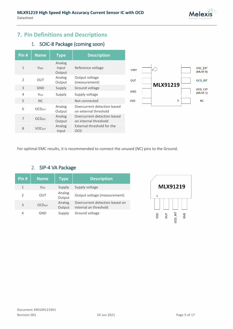
Pin Definitions and Descriptions SOIC-8 Package (coming soon)
Pin # Name Type Description
1 VREF Analog Input
Output Reference voltage
2 OUT Analog Output
Output voltage (measurement)
3 GND Supply Ground voltage
4 VDD Supply Supply voltage
5 NC - Not connected
6 OCDEXT Analog Output
Overcurrent detection based on external threshold
7 OCDINT Analog Output
Overcurrent detection based on internal threshold
8 VOCEXT Analog Input
External threshold for the OCD
For optimal EMC results, it is recommended to connect the unused (NC) pins to the Ground.
SIP-4 VA Package
Pin # Name Type Description
1 VDD Supply Supply voltage
2 OUT Analog Output Output voltage (measurement)
3 OCDINT Analog Output
Overcurrent detection based on internal an threshold
4 GND Supply Ground voltage

MLX91219 High Speed High Accuracy Current Sensor IC with OCD Datasheet
Document 390109121901 Revision 001 24 Jun 2021 Page 6 of 17
Absolute Maximum Ratings
Exceeding the absolute maximum ratings may cause permanent damage. Exposure to absolute maximum-rated conditions for extended periods of time may affect device reliability.
Parameter Value Unit
Positive Supply Voltage (overvoltage) +8 V
Positive Supply Voltage (maintaining application mode) +6.5 V
Reverse Supply Voltage -0.3 V
Positive Pin Voltage (1) VDD + 0.3 V
Output Sourcing Current +25 mA
Reverse Pin Voltage(1) -0.3 V
Output Sinking Current 50 mA
Maximum Junction Temperature, TJ 165 °C
Operating Ambient Temperature Range, TA -40 to +150 °C
Storage Temperature Range, TS -55 to +165 °C
(1) Except for VDD and GND

MLX91219 High Speed High Accuracy Current Sensor IC with OCD Datasheet
Document 390109121901 Revision 001 24 Jun 2021 Page 7 of 17
General Electrical Specification
Operating Parameters TA = -40 to 150°C and VDD=5 V or 3.3 V unless otherwise specified.
Parameter Symbol Test Conditions Min Typ Max Units
Nominal Supply Voltage VDD MLX91219LVA-Axx-5xx 4.5 5 5.5 V
MLX91219LVA-Axx-3xx 3.135 3.3 3.465 V
Supply Current IDD
Without RLOAD, application mode VDD = 5V VDD = 3.3V
15.5 15
19 17
mA mA
Output Resistance ROUT VOUT = 50%VDD, ILOAD = 10 mA 1 5 Ω
Voltage Reference Output Resistance RREF
VREF = 50%VDD, ISINK = 5 mA or ISOURCE = 0.2 mA For SOIC8 version only
120 200 333 Ω
Output Capacitive Load CLOAD Output amplifier stability is optimized for this typical value 0 4.7 6 nF
Output Short Circuit Current ISHORT Output shorted to VDD or VSS - Permanent 100 mA
Output Leakage current ILEAK High impedance mode, TA=150°C 2 20 µA
Output Voltage Linear Swing VOUT_LSW VDD > 4.6 V for Fixed Mode versions 10 90 %VDD
Magnetic specification
Operating Parameters TA = -40 to 150°C unless otherwise specified.
Parameter Symbol Test Conditions Min Typ Max Units
Operational Magnetic Field Range BOP Full scale output range 12 ±500 mT
Linearity Error NL B within BOP, TA = 25°C ±0.5 %FS
Programmable Sensitivity SPROG 4 105 mV/mT
Sensitivity Programming Resolution SRES 0.5 %

MLX91219 High Speed High Accuracy Current Sensor IC with OCD Datasheet
Document 390109121901 Revision 001 24 Jun 2021 Page 8 of 17
Output accuracy specification
Operating Parameters TA = -40 to 150°C, VDD=5 V or 3.3 V and for factory calibrated settings unless otherwise specified.
Parameter Symbol Test Conditions Min Typ Max Units
Voltage Reference(1) VREF TA=25°C, Axx-5xx versions TA=25°C, Axx-3xx versions 2.5
1.65 V V
Thermal Reference Drift(1) ΔTVREF Referred to VREF tbd mV
Lifetime Reference Drift(1) ΔLVREF tbd mV
Voltage Output Quiescent VOQ No magnetic field applied, TA=25°C Axx-5xx versions, VDD = 5V Axx-3xx versions, VDD = 3.3V
2.49 1.64
2.5
1.65
2.51 1.66
V V
Thermal Offset Drift ΔTVOQ
For 5V TA= -40 to 125°C For 5V TA =125 to 150°C For 3.3V TA= -40 to 125°C For 3.3V TA =125 to 150°C
±5 ±8.5 ±7.5 ±8.5
mV mV mV mV
Lifetime Offset Drift(2) ΔLVOQ Compared to level after preconditioning for a given TA -2 2 mV
Ratiometry Offset Error ΔRVOQ For 5V, ±10% VDD For 3.3V, ±5% VDD ±15
±7.5 mV mV
Absolute Sensitivity S
TA=25°C, Axx-500 version Axx-501 version Axx-502 version
7
10 15
mV/mT mV/mT mV/mT
Thermal Sensitivity Drift ΔTS Referred to S, TA= -20°C to 125°C Referred to S, TA= -40°C to 150°C ±1
±2 % %
Lifetime Sensitivity Drift(2) ΔLS Compared to level after preconditioning for a given TA ±1 ±2 %
Ratiometry Sensitivity Error ΔRS VDD= 5V ±10%, 5xx versions TA=25°C
VDD= 3.3V ±5%, 3xx versions TA=25°C -2 -1 +2
+1 % %
Output RMS noise NRMS
TA=25°C, SF=1 *-500 version *-501 version *-502 version
2.8 3.4 4.1
mVRMS
mVRMS
mVRMS
Table 9: Accuracy specifications – analog parameters
(1) Available only with SOIC-8 package, with fixed output (non-ratiometric) only – will be launched soon (2) Lifetime drift data stems from both 1000h HTOL and 2000 cycles TC as per AEC-Q100
The accuracy specifications are defined for the factory calibrated sensitivity and offset. The achievable accuracy is dependent on the user’s end-of-line calibration.

MLX91219 High Speed High Accuracy Current Sensor IC with OCD Datasheet
Document 390109121901 Revision 001 24 Jun 2021 Page 9 of 17
Timing specification Operating Parameters TA = -40 to 150°C, unless otherwise specified.
Parameter Symbol Test Conditions Min Typ Max Units
Step Response Time TRESP Delay between the input signal reaching 90% and the output reaching 90% (see Figure 4)
2.1 µs
Bandwidth BW f-3dB, TA=25°C, SF=1 (factory trim) f-3dB, TA=25°C, SF=2 (programmable) f-3dB, TA=25°C, SF=3 (programmable)
400 200 100
kHz kHz kHz
Power-on Delay TPOD 1 ms
1 µs
in, Vout
time
90%100%Response
time
Figure 4 – Response Time definition
MLX91219 High Speed High Accuracy Current Sensor IC with OCD Datasheet
Document 390109121901 Revision 001 24 Jun 2021 Page 10 of 17
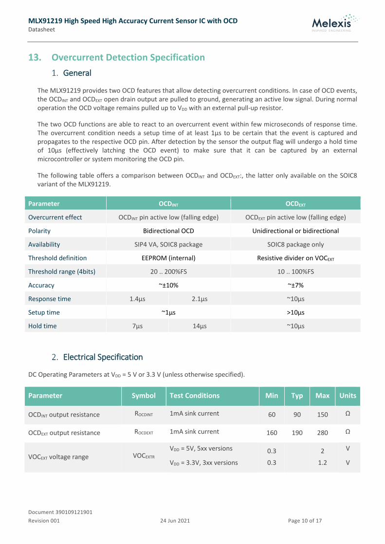
Overcurrent Detection Specification General
The MLX91219 provides two OCD features that allow detecting overcurrent conditions. In case of OCD events, the OCDINT and OCDEXT open drain output are pulled to ground, generating an active low signal. During normal operation the OCD voltage remains pulled up to VDD with an external pull-up resistor.
The two OCD functions are able to react to an overcurrent event within few microseconds of response time. The overcurrent condition needs a setup time of at least 1µs to be certain that the event is captured and propagates to the respective OCD pin. After detection by the sensor the output flag will undergo a hold time of 10µs (effectively latching the OCD event) to make sure that it can be captured by an external microcontroller or system monitoring the OCD pin.
The following table offers a comparison between OCDINT and OCDEXT:, the latter only available on the SOIC8 variant of the MLX91219.
Parameter OCDINT OCDEXT
Overcurrent effect OCDINT pin active low (falling edge) OCDEXT pin active low (falling edge)
Polarity Bidirectional OCD Unidirectional or bidirectional
Availability SIP4 VA, SOIC8 package SOIC8 package only
Threshold definition EEPROM (internal) Resistive divider on VOCEXT
Threshold range (4bits) 20 .. 200%FS 10 .. 100%FS
Accuracy ~±10% ~±7%
Response time 1.4µs 2.1µs ~10µs
Setup time ~1µs >10µs
Hold time 7µs 14µs ~10µs
Electrical Specification
DC Operating Parameters at VDD = 5 V or 3.3 V (unless otherwise specified).
Parameter Symbol Test Conditions Min Typ Max Units
OCDINT output resistance ROCDINT 1mA sink current 60 90 150 Ω
OCDEXT output resistance ROCDEXT 1mA sink current 160 190 280 Ω
VOCEXT voltage range VOCEXTR VDD = 5V, 5xx versions
VDD = 3.3V, 3xx versions
0.3
0.3
2
1.2
V
V

MLX91219 High Speed High Accuracy Current Sensor IC with OCD Datasheet
Document 390109121901 Revision 001 24 Jun 2021 Page 11 of 17
Internal Overcurrent Detection Principle
The internal OCD takes fixed threshold voltage values predefined in the EEPROM and do not require any extra components. The OCDINT implementation allows detecting overcurrent outside of the output measurement range of the sensor and is therefore suitable for large current peaks as occurring during short-circuit. If the theoretical sensor output overcomes the OCDINT voltage threshold, the overcurrent event is flagged on OCDINT pin. The default OCD threshold voltages are defined as follow, but other values can be set on request.
Ordering Code Sensitivity [mV/mT]
OCDINT Factory trimmed Threshold Level [%FS]
OCDINT Factory trimmed Threshold Level [mT]
MLX91219LVA-AAA-500 7 128 %FS 366 mT
MLX91219LVA-AAA-501 10 128 %FS 256 mT
MLX91219LVA-AAA-502 15 128 %FS 170 mT
Table 13: OCDINT threshold currents
External Overcurrent Detection Principle The external OCD uses the voltage applied on VOCEXT pin as threshold voltage. This translates into an overcurrent threshold depending on the sensitivity of the sensor. A voltage divider on VOCEXT allows defining the threshold voltage in a custom way. Depending on the voltage divider configuration, the OCDEXT can be used either in bidirectional or unidirectional mode. The External OCD threshold is defined within the measurement range of the sensor output. It offers a better accuracy than OCDINT but the response is slower. The below table presents the unidirectional and bidirectional external OCD configurations. Please refer to section 14 for more details about the application diagram and the recommended resistances.
Bidirectional configuration Unidirectional configuration
R3 R4 R4bis R3

MLX91219 High Speed High Accuracy Current Sensor IC with OCD Datasheet
Document 390109121901 Revision 001 24 Jun 2021 Page 12 of 17
𝑉𝑉𝑉𝑉𝐶𝐶𝐸𝐸𝐸𝐸𝐸𝐸 = 𝑉𝑉𝑅𝑅𝐸𝐸𝑅𝑅 ∗𝑅𝑅3
𝑅𝑅3 + 𝑅𝑅4
𝑉𝑉𝑉𝑉𝑉𝑉𝑉𝑉𝑉𝑉 = 𝑉𝑉𝑉𝑉𝐶𝐶𝐸𝐸𝐸𝐸𝐸𝐸
𝑉𝑉𝑉𝑉𝑉𝑉𝑉𝑉𝑉𝑉 = 2.𝑉𝑉𝑅𝑅𝐸𝐸𝑅𝑅 − 𝑉𝑉𝑉𝑉𝑉𝑉𝑉𝑉𝑉𝑉
𝑉𝑉𝑉𝑉𝐶𝐶𝐸𝐸𝐸𝐸𝐸𝐸 = 𝑉𝑉𝑅𝑅𝐸𝐸𝑅𝑅 + (𝑉𝑉𝐷𝐷𝐷𝐷 − 𝑉𝑉𝑅𝑅𝐸𝐸𝑅𝑅) ∗𝑅𝑅3
𝑅𝑅3 + 𝑅𝑅4𝑏𝑏𝑏𝑏𝑏𝑏
𝑉𝑉𝑉𝑉𝑉𝑉𝑉𝑉𝑉𝑉 = 𝑉𝑉𝑉𝑉𝐶𝐶𝐸𝐸𝐸𝐸𝐸𝐸
Recommended Application Diagram SOIC-8 Package
Part Description Value Unit
C1 Supply capacitor, EMI, ESD 47 nF
C2 Decoupling, EMI, ESD 4.7 nF
C3 Decoupling, EMI, ESD 47 nF
R1 Internal OCD resistor 10 kΩ
R2 External OCD resistor 10 kΩ
R3/R4/R4bis Uni-/Bidirectional OCD customized ratio - kΩ

MLX91219 High Speed High Accuracy Current Sensor IC with OCD Datasheet
Document 390109121901 Revision 001 24 Jun 2021 Page 13 of 17
SIP-4 VA Package
Part Description Value Unit
C1 Supply capacitor, EMI, ESD 47 nF
C2 Decoupling, EMI, ESD 4.7 nF
R1 Internal OCD resistor 10 kΩ
MLX91219

MLX91219 High Speed High Accuracy Current Sensor IC with OCD Datasheet
Document 390109121901 Revision 001 24 Jun 2021 Page 14 of 17
Standard Information
Our products are classified and qualified regarding soldering technology, solderability and moisture sensitivity level according to following test methods:
Reflow Soldering SMD’s (Surface Mount Devices)
▪ IPC/JEDEC J-STD-020
Moisture/Reflow Sensitivity Classification for Nonhermetic Solid State Surface Mount Devices (classification reflow profiles according to table 5-2)
▪ EIA/JEDEC JESD22-A113
Preconditioning of Nonhermetic Surface Mount Devices Prior to Reliability Testing (reflow profiles according to table 2)
Wave Soldering SMD’s (Surface Mount Devices) and THD’s (Through Hole Devices)
▪ EN60749-20
Resistance of plastic- encapsulated SMD’s to combined effect of moisture and soldering heat
▪ EIA/JEDEC JESD22-B106 and EN60749-15
Resistance to soldering temperature for through-hole mounted devices
Iron Soldering THD’s (Through Hole Devices)
▪ EN60749-15
Resistance to soldering temperature for through-hole mounted devices
Solderability SMD’s (Surface Mount Devices) and THD’s (Through Hole Devices)
▪ EIA/JEDEC JESD22-B102 and EN60749-21
Solderability
For all soldering technologies deviating from above mentioned standard conditions (regarding peak temperature, temperature gradient, temperature profile etc) additional classification and qualification tests have to be agreed upon with Melexis. The application of Wave Soldering for SMD’s is allowed only after consulting Melexis regarding assurance of adhesive strength between device and board.
Melexis recommends reviewing on our web site the General Guidelines soldering recommendation (https://www.melexis.com/en/quality-environment/soldering).
Melexis is contributing to global environmental conservation by promoting lead free solutions. For more information on qualifications of RoHS compliant products (RoHS = European directive on the Restriction Of the use of certain Hazardous Substances) please visit the quality page on our website (https://www.melexis.com/en/quality-environment).
MLX91219 High Speed High Accuracy Current Sensor IC with OCD Datasheet
Document 390109121901 Revision 001 24 Jun 2021 Page 15 of 17
ESD Precautions Electronic semiconductor products are sensitive to Electro Static Discharge (ESD). Always observe Electro Static Discharge control procedures whenever handling semiconductor products.
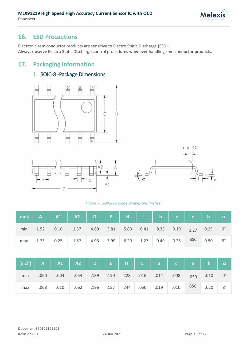
Packaging information SOIC-8 -Package Dimensions
Figure 7 : SOIC8 Package Dimensions [inches]
[mm] A A1 A2 D E H L b c e h α
min 1.52 0.10 1.37 4.80 3.81 5.80 0.41 0.35 0.19 1.27
BSC
0.25 0°
max 1.73 0.25 1.57 4.98 3.99 6.20 1.27 0.49 0.25 0.50 8°
[inch] A A1 A2 D E H L b c e h α
min .060 .004 .054 .189 .150 .228 .016 .014 .008 .050
BSC
.010 0°
max .068 .010 .062 .196 .157 .244 .050 .019 .010 .020 8°
MLX91219 High Speed High Accuracy Current Sensor IC with OCD Datasheet
Document 390109121901 Revision 001 24 Jun 2021 Page 16 of 17
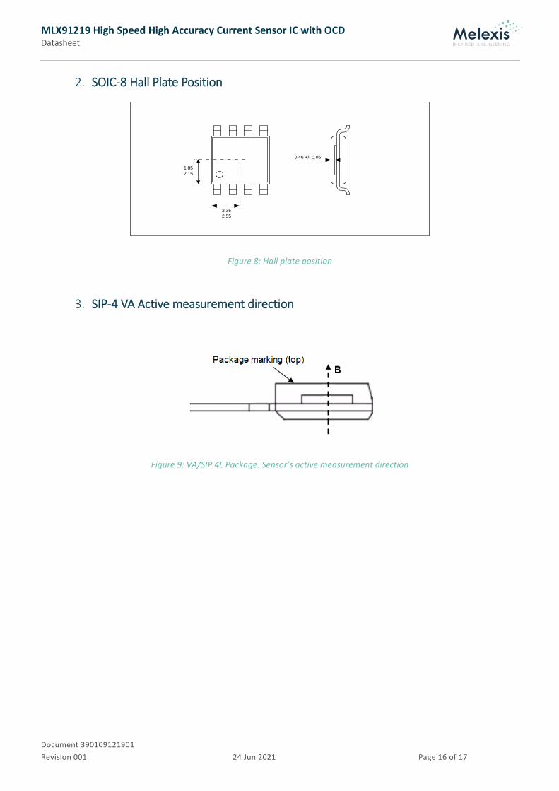
SOIC-8 Hall Plate Position
1.852.15
2.352.55
0.46 +/- 0.06
Figure 8: Hall plate position
SIP-4 VA Active measurement direction
Figure 9: VA/SIP 4L Package. Sensor’s active measurement direction

MLX91219 High Speed High Accuracy Current Sensor IC with OCD Datasheet
Document 390109121901 Revision 001 24 Jun 2021 Page 17 of 17
Disclaimer The content of this document is believed to be correct and accurate. However, the content of this document is furnished "as is" for informational use only and no representation, nor warranty is provided by Melexis about its accuracy, nor about the results of its implementation. Melexis assumes no responsibility or liability for any errors or inaccuracies that may appear in this document. Customer will follow the practices contained in this document under its sole responsibility. This documentation is in fact provided without warranty, term, or condition of any kind, either implied or expressed, including but not limited to warranties of merchantability, satisfactory quality, non-infringement, and fitness for purpose. Melexis, its employees and agents and its affiliates' and their employees and agents will not be responsible for any loss, however arising, from the use of, or reliance on this document. Notwithstanding the foregoing, contractual obligations expressly undertaken in writing by Melexis prevail over this disclaimer. This document is subject to change without notice, and should not be construed as a commitment by Melexis. Therefore, before placing orders or prior to designing the product into a system, users or any third party should obtain the latest version of the relevant information. Users or any third party must determine the suitability of the product described in this document for its application, including the level of reliability required and determine whether it is fit for a particular purpose. This document as well as the product here described may be subject to export control regulations. Be aware that export might require a prior authorization from competent authorities. The product is not designed, authorized or warranted to be suitable in applications requiring extended temperature range and/or unusual environmental requirements. High reliability applications, such as medical life-support or life-sustaining equipment or avionics application are specifically excluded by Melexis. The product may not be used for the following applications subject to export control regulations: the development, production, processing, operation, maintenance, storage, recognition or proliferation of: 1. chemical, biological or nuclear weapons, or for the development, production, maintenance or storage of missiles for such weapons; 2. civil firearms, including spare parts or ammunition for such arms; 3. defense related products, or other material for military use or for law enforcement; 4. any applications that, alone or in combination with other goods, substances or organisms could cause serious harm to persons or goods and that can be used as a means of violence in an armed conflict or any similar violent situation. No license nor any other right or interest is granted to any of Melexis' or third party's intellectual property rights. If this document is marked “restricted” or with similar words, or if in any case the content of this document is to be reasonably understood as being confidential, the recipient of this document shall not communicate, nor disclose to any third party, any part of the document without Melexis’ express written consent. The recipient shall take all necessary measures to apply and preserve the confidential character of the document. In particular, the recipient shall (i) hold document in confidence with at least the same degree of care by which it maintains the confidentiality of its own proprietary and confidential information, but no less than reasonable care; (ii) restrict the disclosure of the document solely to its employees for the purpose for which this document was received, on a strictly need to know basis and providing that such persons to whom the document is disclosed are bound by confidentiality terms substantially similar to those in this disclaimer; (iii) use the document only in connection with the purpose for which this document was received, and reproduce document only to the extent necessary for such purposes; (iv) not use the document for commercial purposes or to the detriment of Melexis or its customers. The confidentiality obligations set forth in this disclaimer will have indefinite duration and in any case they will be effective for no less than 10 years from the receipt of this document. This disclaimer will be governed by and construed in accordance with Belgian law and any disputes relating to this disclaimer will be subject to the exclusive jurisdiction of the courts of Brussels, Belgium. The invalidity or ineffectiveness of any of the provisions of this disclaimer does not affect the validity or effectiveness of the other provisions. The previous versions of this document are repealed. Melexis © - No part of this document may be reproduced without the prior written consent of Melexis. (2021) IATF 16949 and ISO 14001 Certified
For the latest version of this document or find your local contact, visit us at www.melexis.com