mmiiddaas s sseettuup bp blloocck k ddiiagag
TRANSCRIPT

P
MIDAS SetUp block Diag.MIDAS SetUp block Diag.
Detector
Data ACQ
P
SHAP
AMUX ADC LTC
SHAP
Gain
BUS
16 CH
G_SelSOC
EOC
LEN
MUX Add
12Bit Data
T/H
x2x4x8
A
SHDSP
INTERF.
24Bit Data
G_SelT/H
MUX_AddSOCEOCLEN
DSP.
DATA
DATA
ADD & CTR
ADD & CTR
CFD Trig.Logic
Thr
TU2
TU1
EOC
IRQB
IRQA
STR
STR
EM
OUT
TRIG
DLY
TRIG(T/H)
H
T

x16
PaPa A/ShapA/ShapMUX
MUX
AdAd2.2nF
G : x2
CFDCFD Trigg
AA ADC
Zin cfd~50
2.2nF
B: 1/2
Tst_In
S_In
3
2

Pa
Pa
D6LOLFRQ'HWHFWRU
�9G
B
B
B
B
7
6
7
6
10M
�
10M
�Cathode(Sectors & Comm.Sideof Quad. Det.)
Anode(Rings & Quadrant)
Pol. Voltage
DecouplingCapacitors
OutputBuffers
3UH$P
�
2XWSX
�
6LJQDOV3UH$P
�
2XWSX
�
6LJQDOV

'HWHFWRUV'HWHFWRUV
Rings DetectorRings Detector Quadrant DetectorQuadrant Detector
p – type(anode)48 ring channels
n – type(cathode)16 sector channels
Front Side :4 p-type Quadrants
Back Side :Common n-type Layer( not read )

'HWHFWRUV'HWHFWRUV
Kaptonflex printed circuit

1 4 10 8
2
3 6
7
5 9
6
7
Test_IN
Signal_IN
*
* on the hybrid there is an additional parasitic capacitance of abou 1pF do to the layout
Gi = 1mV/fC
?
out\
out
+6 GND -6 OFFSET ADJ.
1pF
1pF
820
15nF
8K2
100M
390
3UH$P
�
%ORF
�
GLDJ3UH$P
�
%ORF
�
GLDJ

+Vd
+6 -6
-6
-6
T_IN
S_IN
-6
Out n_i
Out inv
diff. output( 50 ohm )
To pol. voltage for cathodes
To GND for anodes(rings and quadrants)
are not read
(sectors and common sidesof quad. det.)
out. offset adj.
N.B. The common sides of the quad. det.
TESTIN out
SIGN out/
50
10MC9124
10nF
4.7K2K
4.7K
3.9K
8208.2K
15nF
3.9K
PRE 4500
3
2
8
6
7
5 9
3UH$P
�
FRQILJ3UH$P
�
FRQILJ

3UH$PS � %RDU
�
3UH$PS � %RDU
�

3UH$P
�
&RSSH � %R[3UH$P
�
&RSSH � %R[
Output Connector Side
R1-1 R1-2 S1 R2-1 R2-2 S2 Q1 Q2 Q3
PreAmp OutputConnectors
PreAmpTst In
PreAmp BoardPower Supply
Tr1
Tr24
PreAmp OutOffset Adj
1
24
1
16
1
4
GND
1
24

32
31
30
29
28 A2427 A2326 A2225 A2124 A2023 A1922
21 A1820 A1719
18
17 A1616 A1515 A1414 A1313 A1212 A1111 A1010 A099
8 A087 A076 A065 A054 A043 A032 A021 A01
3UH$P
�
2XWSX
�
&RQQHFWRUV3UH$P
�
2XWSX
�
&RQQHFWRUV
32
31
30
29
28 A4827 A4726 A4625 A4524 A4423 A4322
21 A4220 A4119
18
17 A4016 A3915 A3814 A3713 A3612 A3511 A3410 A339
8 A327 A316 A305 A294 A283 A272 A261 A25
A C
32
31
30
29
28
27
26
25
24
23
22
21
20
19
18
17 S1616 A1515 S1414 S1313 S1212 S1111 S1010 S099
8 S087 S076 S065 S054 S043 S032 S021 S01
A C
32
31
30
29
28
27
26
25
24
23
22
21
20
19
18
17
16
15
14
13
12
11
10
9
8
7
6
5 Q44 Q33
2 Q21 Q1
A C
R1 R2 S
A C
Q
Row A : non-inv. Out - positive signals for Rings & Quadrant ; negative for SectorsRow C : inverting Out - negative signals for Rings & Quadrant ; positive for Sectors
DIN 64 Male
Gnd ;

A C
R1
32
31
30
29
28A2427A2326A2225A2124A2023A1922
21A1720A1619
18
17A1316A1215A1114A1013A0912A0811A0710A069
8A047A036A025A014
3
2
1
GR
A05
A14
A15
A18
A C
R2
32
31
30
29
28A4827A4726A4625A4524A4423A4322
21A4120A4019
18
17A3716A3615A3514A3413A3312A3211A3110A309
8A287A276A265A254
3
2
1
A29
A38
A39
A42
A C
S
32
31
30
29
28
27
26
25
24
23
22
21
20S1619
18
17S1316S1215S1114S1013S0912S0811S0710S069
8S047S036S025S014
3
2
1
GR
S05
S14
S15
A C
Q
32
31
30
29
28
27
26
25
24
23
22
21
20
19
18
17
16
15
14
13
12
11
10
9
8Q037
6Q025Q014
3
2
1
Q04
3UH$P
�
,QSX
�
&RQQHFWRUV3UH$P
�
,QSX
�
&RQQHFWRUV
GR
All Rings & Quadrants are referred to Gnd through a 10M resistor ; GR , for R and Q, to Gnd through a 1M res.All Sectors are referred to +Vd through a 10M resistors ; related GR is referred to +Vd through a 1M res.Commond Sides of Quadrant Detectors( pin 30 ) are referred to +Vd through a 10M resistor.
GuardRing
+VdShiels
DIN 64 Female

0+
SENSING 0+SENSING 0-0-
1+
SENSING 1+
SENSING 1-1-
2+SENSING 2+SENSING 2-2-
3+SENSING 3+
SENSING 3-3-
ROSSO
ARANCIOGRIGIONERO
BIANCO
ROSAMARRONE
BLU
ROSSOARANCIOGRIGIONERO
BIANCOMARRONE
ROSABLU
P2
POWER 1
594837261
P3
POWER 2
594837261
P1
GENERAL PWR
19371836173516341533143213311230112910289278267256245234223212201
3UH$P
�
3ZU6XSSO � &DEOH3UH$P
�
3ZU6XSSO � &DEOH
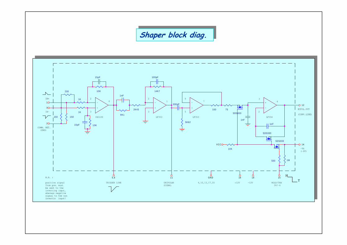
positive signalfrom pre. mustbe sent to theinverting input,whereas negativesignal to the noninvertin input!
N.B. : 5,6 11 15G N D 16 18
1
3
2
V C C
12
14
+
-
3
2
6
+
-
+
-
+
-
2
3
62
3
16
5
7
CA3100 LF353 LF353 LF356
HOLD/TRA0V/-6
-Vb(-6V)
BIPOL.OUT
-12V+12V4,10,13,17,20
IN+
IN-
COMM. RET.(GND)
TRIGGER LINE UNIPOLARSIGNAL
(CONV.LINE)
75100
5 K 6 2
1 4 K 71 0 K
1 K
1 K
15pF 100pF
15pF
1509 K 1
2 K 4 3
1 0 K
200
1nF
1 0 K
S D 5 0 0 0
S D 5 0 0 0
1nF
1nF
S D 5 0 0 0
330pF
1 M500
150
H
T
6KDSH � EORF
�
GLDJ��6KDSH � EORF
�
GLDJ��

1
2
3
Shield
8
8
8
Shielded Twisted Pair Cable
DIN 64FEM.
To PreAmpBoard Out Conn.
To Shap/ADCBoards
24 Diff.SignalLines
3UH$P � ² 6KDS�$'
�
%RDUG � ,QWHUFRQQHFWLRQ3UH$P � ² 6KDS�$'
�
%RDUG � ,QWHUFRQQHFWLRQ
~ 6 mt
Coloured Wires : to the row C , PreAmp invertig Outputs
White Wires : to the row A ; PreAmp non-inv. Outputs
gnd

Beam Line
R1 R2 Q1 Q2 Q3
Pb1 Pb2
Beam Line
QuadrantDetectors
RingsDetectors
Lead
(Tracking)
(Absorber)Only Quad. Det. are used to combine Triggers
Pion Trigger ( i pioni “bucano” l’ intero telescopio) :
�t = Q1&Q2&Q3 ( low level threshold )
Proton Trigger ( i protoni si fermano in Pb1 od alpiù in Pb2 ) :
Pt = Q1+Q2 ( high level threshold )
Where Q1 = �i Q1i , the Or(wired) of the four sectorsof the single Qad Det .
Same for Q2 and Q3 .

D2+
-
Ad+
-
Drv
Ck
D
D1+
-Inibit
ThresholdAdj
Atten.
Del. line
Walk adj
&)'
Signalsfrom
PreAmp
ECL lineDriver
Leading EdgeArming Disc.
Sum & 0xDetector
PulseFormer
Diff. Ampl.( A x2 )
Decoupling &Diff. Capacitor
�&K7LJ�
6LQJO � FK��WULJ � &RQILJ�6LQJO � FK��WULJ � &RQILJ�
There are two CFD for each channel of Quad. Det. :One for LowLevel Threshold ( � trigg. ) ; andOne for HighLevel Threshold ( p trigg. )
10EL31
AD8001
AD96687
10E116

C F D 4
C F D 4
IN7IN8
T H RQ14
C F D 5
C D F 5
IN9IN10
T H RQ21
C F D 6
C F D 6
IN11IN12
T H RQ22
C F D 7
C F D 7
IN13IN14
T H RQ23
C F D 9
C F D 9
IN17IN18
T H RQ31
CFD10
CFD10
IN19IN20
T H RQ32
CFD12
CFD12
IN23IN24
T H RQ34
C F D 2
C F D 2
IN3IN4
T H RQ12
C F D 1
C F D 1
IN1IN2
T H RQ11
C F D 3
C F D 3
IN5IN6
T H RQ13
C F D 8
C F D 8
IN15IN16
T H RQ24
CFD11
CFD11
IN21IN22
T H RQ33
V E E
V E E
V E E
V E E
V E E
-5.2
NIM
NIM
NIM
NIM
Q1 Quad Or
Q2 Quad Or
Q3 Quad Or
TRIG
NIM
TRIG
Soglia bassa
Soglia alta
Trigger
Pioni
Trigger
Protoni
Threshold Adj.
OR*Q1
OR*Q2OR*Q3
OR*Q1
OR*Q2
OR*Q3
AND123
OR12
OR12
IN11
IN18IN9
IN20
IN10
IN16
IN2
IN12
IN5
T H R
IN4
IN24
IN19
IN8
IN3
IN22IN14IN21
IN23
IN13
IN15
IN6
IN17
IN7
IN1
AND123
O R Q 1O R Q 2
Q72N3546
R270100
J8
Q62N3546
R269100
J7
Q52N3546
R263100
J6
JP36
Q32N3546
R260100
J4
JP39
JP42
JP45
JP37
JP40
JP43
JP38
JP41
JP47
Q42N3546
R262100
J5
JP46
SY10EL01
D 01
D 12
D 23
D 34Q
6
Q7
MC10E116
34
89
2
MC10E116
34
89
2
JP44
MC10E116
34
89
2
SY10EL01
D 01D 12
D 23D 34
Q6
Q7
IN[1..24]
ArrangingTriggers
ArrangingTriggers
Q1 Q2 Q3

�
Q1LLT
(10E116)
�
Q1LLT
(10E116)
�
Q1HLT
(10E116)
�
Q1HLT
(10E116)
S1 S2
AD8001AD
8001
10EL3110
EL31
AD96687
AD96687
AD8001AD
8001
10EL31
10EL31
AD96687
AD96687
DLLLT
2
DLLLT
2
DLLLT
1
DLLLT
1
DLHLT
2
DLHLT
2
DLHLT
1
DLHLT
1
J1
THR/H
THR/L
HLT
LLT
Ch1
Ch3
Ch2Ch1
Ch4
Gnd
( Ch2 on the rear )
TInTIn
Trig BoardComp. Side
J2
Ch3
Ch2Ch1
Ch4
Gnd
Q1
Q2
1 2 3 4 1 2 3 4Quadrant Wired Or
Single Channelsjumpers
1
2
3
5
4
DL
DelayLine5 steps ; 40 ns total del.Actual sel. 32n ( jp 4 )
LL HLOr Q1
Or Q2
Or Q3
T � Tp
Front Panel view ;Trigger OutputConnectors (NIM)
Q1 Q2 Q3
Q1
Q2
Q3
1 2
3 4
7ULJ��/D\RXW7ULJ��/D\RXW
1
1
LEN
EOC
Board Selectionjumpers
Shapers Disposition

LEN
EOC
S1 S2
AC374
AC374
AC374
AC374
AC374
AC374
AC374
AC374
1
1
S9 S10
9HUWH
�
%RDUG9HUWH
�
%RDUG
1 2 3 4
Vert. BoardComp. Side
Ch 1
Ch 8
Ch 9
Ch 16
Gnd
Gnd5 6 7 8
9 10 11 12 13 14 15 16
Diff. Tst_In(remote shap. testing)
ADC DataLatches
Group 1: to the lower partof DataBus ( DB [0..11] )
Group 2: to the upper part
of DataBus ( DB [12..23] )
BoardSelection
Shapers Disposition
Only one group at a timeis alternatively mountedon the Boards
LEN(Latch Enable) select the coupleof Boards read at a time ;EOC(EndOfConv) select the numberof the Board

GND
GND
GND
GND
+5DC
+5DC
DB0 H/T_1DB1DB2
AD1
DB3
AD2
DB4
AD3
DB5DB6DB7DB8DB9DB10DB11
DB12DB13DB14DB15DB16DB17
SOC
DB18DB19
EOC*1DB20
EOC*2DB21
EOC*3DB22
EOC*4DB23
EOC*5LEN*1
EOC*6LEN*2
EOC*7LEN*3
EOC*8LEN*4
EOC*9LEN*5
EOC*10
G_SEL1G_SEL2
TSTIN5TSTIN4TSTIN3TSTIN2
TSTIN6TSTIN7TSTIN8
TSTIN1
H/T_2
AD0
J13
VMECONN1
NC1A
NC2A
NC3A
NC4A
NC5A
NC6A
NC7A
NC8A
NC9A
NC10A
NC11A
NC12A
NC13A
NC14A
NC15A
NC16A
NC17A
NC18A
NC19A
NC20A
NC21A
NC22A
NC23A
NC24A
NC25A
NC26A
NC27A
NC28A
NC29A
NC30A
NC31A
NC32A
+5V1B
GND2B
NC3B
A244B
A255B
A266B
A277B
A288B
A299B
A3010B
A3111B
GND12B
+5V13B
D1614B
D1715B
D1816B
NC1C
NC2C
NC3C
NC4C
NC5C
NC6C
NC7C
NC8C
NC9C
NC10C
NC11C
NC12C
NC13C
NC14C
NC15C
NC16C
NC17C
NC18C
NC19C
NC20C
NC21C
NC22C
NC23C
NC24C
NC25C
NC26C
NC27C
NC28C
NC29C
NC30C
NC31C
NC32C
D1917B
D2018B
D2119B
D2220B
D2321B
GND22B
D2423B
D2524B
D2625B
D2726B
D2827B
D2928B
D3029B
D3130B
GND31B
+5V32B
LEN
EOC
AC374
AC374
AC374
AC374
1
1
BoardSelection
Bd 1
LEN
EOC
AC374
AC374
AC374
AC374
1
1
BoardSelection
Bd 2
LEN
EOC
AC374
AC374
AC374
AC374
AC374
AC374
AC374
AC374
1
1
BoardSelection
Bd 9
Vertex Boards
Trigger Board •On Trig.B. both group oflatches are present
DSP Raw Data Buffer :
x:$2000 000000 000000 000000 000000 ...
x:$2006 000000 000000 000000 000000 ...
x:$200c 000000 000000 000000 000000 ...
.......
x:$2042 000000 000000 000000 000000
x:$2000 000000 000000 ... ... 000000
DSP Raw Data Buffer :
x:$2000 000000 000000 000000 000000 ...
x:$2006 000000 000000 000000 000000 ...
x:$200c 000000 000000 000000 000000 ...
.......
x:$2042 000000 000000 000000 000000
x:$2000 000000 000000 ... ... 000000
There are 8 boards for Vertex(Rings)Detectors and 1 board for Quadrant(Triggers) Detectors
9 Bd ; 16ch/Bd 144 ch tot.
Bd1 Bd2 Bd9 Bd10
Ch 1

MidVert
MidVert
MidVert
MidVert
MidVert
MidVert
MidVert
MidVert
MidTrig
1
2
31
2
A
D
Trig
EC
Int
21 3 4 5 6 7 8 9
R1/1 R1/2 R1/3 S1 R2/1 R2/2 R2/3 S2 Q1/2/3
6KDSHUV�$'
�
%RDUGV90
�
&UDWH6KDSHUV�$'
�
%RDUGV90
�
&UDWH
DSP-Shap/ADC Interface Bd.
Ring Det. 1
Ring Det. 2
Quadrant Detectors( Triggers Bd. )

'63�$F � 7LPLQ � 'LDJUDP'63�$F � 7LPLQ � 'LDJUDP
Starting Acq Prog.
Fix Gain Sel “ x2” ( G_Sel1 , G_Sel2 = 0 )
Send a first “ SOC” to inizialize the ADCCKEN ;
HTEN ; Preset the T/H signal in “T rack” mode
H/T ; ( Track and Hold signal of the Shapers in Track mode)
Wait for an IRQA (ext. “T rigg” ) signal
IRQA(“T RIGGER” )
H/T ; (Hold mode)
A0
A1
A2
A3
Select first Mux channel
SOC ; Send(CKEN) a “ Start of Conv.” to the ADC
IRQB (“ End of Conv.” – EOC- signal from all ADC )
LEN1 ; Read and Store Bd 1,2
LEN2 ; Read and Store Bd 3,4
LEN5 ; Read and Store Bd 9,10 ;
Select next Mux channel ; Send the SOC ; Receive the EOC(IRQB) ; Read and Store the channel value of all the boards .So on till channel 16 ;....Then : Release the Hold signal (set H/T in Track mode);
Enable again IRQA and wait for another Trigger .
Disable IRQA and Enable IRQB