mobile i/o companion support keyscan, i/o expansion ... clock required – dedicated slow clock...
TRANSCRIPT
LM8325-1
www.ti.com SNLS347A –SEPTEMBER 2011–REVISED MARCH 2013
LM8325-1 Mobile I/O Companion Supporting Keyscan, I/O Expansion, PWM, andACCESS.bus Host Interface
Check for Samples: LM8325-1
1FEATURES etc.)• KEY DEVICE FEATURES
2• KEY FEATURES– 1.8V ± 10% Single-supply Operation– Internal RC Oscillator, No External Clock
Required – On-chip Power-on Reset (POR)– Internal PWM Clock Generation, No – Watchdog Timer
External Clock Required – Dedicated Slow Clock Input for 32 kHz to– Programmable I2C-compatible ACCESS.bus 2MHz
Address (Default 0x88) – −40°C to +85°C Temperature Range– Support for Keypad Matrices of up to of 8 x – 25-pin csBGA Package
12 Keys, Plus 8 Special Function (SF) Keys,for a Full 104 Key Support APPLICATIONS
– I2C-compatible ACCESS.bus Slave Interface • Cordless Phonesat 100 kHz (Standard-Mode) and 400 kHz
• Smart Handheld Devices(Fast-Mode)• Keyboard Applications– Three Host-programmable PWM Outputs
for Smooth LED Brightness ModulationDESCRIPTION
– Supports General-purpose I/O ExpansionThe LM8325-1 GenI/O - Expander and Keypadon Pins Not Otherwise Used for Keypad or Controller is a dedicated device to unburden a host
PWM Output processor from scanning a matrix-addressed keypad– 15 Byte Key Event Buffer and to provide flexible and general purpose, host
programmable input/output functions. Three– Multiple Key Event Storageindependent PWM timer outputs are provided for
– Key Events, Errors, and Dedicated dynamic LED brightness modulation.Hardware Interrupts Request Host Service
It communicates with a host processor through anby Asserting an IRQ OutputI2C-compatible ACCESS.bus serial interface. It can– Automatic HALT Mode for Low Power communicate in Standard (100 kHz) - and Fast-Mode
Operation (400 kHz) in slave Mode only.– Wake-up from HALT Mode on Any Interface
All available input/output pins can alternately be used(Rising Edge, Falling Edge or Pulse)as an input or an output in a keypad matrix or as a
– Three PWM Outputs with Dedicated Script host programmable general purpose input or output.Buffer for up to 32 Commands
Any pin programmed as an input can also sense– Register-based Command Interpreter with hardware interrupts. The interrupt polarity (“high to
Auto Increment Address low” or “low to high” transition) is thereby• HOST-CONTROLLED FEATURES programmable.
– PWM Scripting for Three PWM Outputs The LM8325-1 follows a predefined register basedset of commands. Upon startup (power - on) a– Period of Inactivity That Triggers Entry intoconfiguration file must be sent from the host to setupHALT Modethe hardware of the device.– Debounce Time for Reliable Key Event
Polling– Configuration of General Purpose I/O Ports– Various Initialization Options (Keypad Size,
1
Please be aware that an important notice concerning availability, standard warranty, and use in critical applications ofTexas Instruments semiconductor products and disclaimers thereto appears at the end of this data sheet.
2All trademarks are the property of their respective owners.
PRODUCTION DATA information is current as of publication date. Copyright © 2011–2013, Texas Instruments IncorporatedProducts conform to specifications per the terms of the TexasInstruments standard warranty. Production processing does notnecessarily include testing of all parameters.

LM8325-1
SNLS347A –SEPTEMBER 2011–REVISED MARCH 2013 www.ti.com
LM8325-1 FUNCTION BLOCKS
PIN ASSIGNMENTS
Figure 1. LM8325-1 Pinout — Top View
2 Submit Documentation Feedback Copyright © 2011–2013, Texas Instruments Incorporated
Product Folder Links: LM8325-1

LM8325-1
www.ti.com SNLS347A –SEPTEMBER 2011–REVISED MARCH 2013
SIGNAL DESCRIPTIONS
DEVICE PIN FUNCTIONS
KEY AND ALTERNATE FUNCTIONS OF ALL DEVICE PINSBall Function 0 Function 1 Function 2 Function 3 Pin Count Ball Name
C2 Slow Clock Input 1 CLKIN
A4 Supply Voltage 1 VCC
D1 Main I2C - Clk 1 SCL
D2 Main I2C - data 1 SDA
C5 Keypad-I/O X0 Genio0 1 KPX0
A5 Keypad-I/O X1 Genio1 1 KPX1
E1 Keypad-I/O X2 Genio2 1 KPX2
E2 Keypad-I/O X3 Genio3 1 KPX3
A2 Keypad-I/O X4 Genio4 1 KPX4
B3 Keypad-I/O X5 Genio5 1 KPX5
A3 Keypad-I/O X6 Genio6 1 KPX6
B4 Keypad-I/O X7 Genio7 1 KPX7
E5 Keypad-I/O Y0 Genio8 1 KPY0
C4 Keypad-I/O Y1 Genio9 1 KPY1
D5 Keypad-I/O Y2 Genio10 1 KPY2
B5 Keypad-I/O Y3 Genio11 1 KPY3
B2 Keypad-I/O Y4 Genio12 1 KPY4
A1 Keypad-I/O Y5 Genio13 1 KPY5
B1 Keypad-I/O Y6 Genio14 1 KPY6
C1 Keypad-I/O Y7 Genio15 1 KPY7
D4 Keypad-I/O Y8 Genio16 ClockOut PWM2 1 KPY8
PWM2
E4 Keypad-I/O Y9 Genio17 PWM1 1 KPY9
PWM1
D3 Keypad-I/O Y10 Genio18 PWM0 1 KPY10
PWM0
E3 Interrupt Keypad-I/O Y11 Genio19 PWM2 1 IRQN
KPY11
PWM2
C3 Ground 1 GND
TOTAL 25
PIN CONFIGURATION AFTER RESET
Upon power-up or RESET the LM8325-1 will have defined states on all pins. provides a comprehensive overviewon the states of all functional pins.
Copyright © 2011–2013, Texas Instruments Incorporated Submit Documentation Feedback 3
Product Folder Links: LM8325-1

LM8325-1
SNLS347A –SEPTEMBER 2011–REVISED MARCH 2013 www.ti.com
Pin Configuration after ResetPins Pin States
KPX0
KPX1
KPX2
KPX3Full Buffer mode with an on-chip pull up resistor enabled.
KPX4
KPX5
KPX6
KPX7
KPY0
KPY1
KPY2
KPY3
KPY4
KPY5 Full Buffer mode with an on-chip pull down resistor enabled.
KPY6
KPY7
KPY8 / PWM2
KPY9 / PWM1
KPY10 / PWM0
KPY11 / IRQN / PWM2 Open Drain mode with no pull resistor enabled, driven low (IRQN). (1)
SCL Open Drain mode with no pull resistor enabled.SDA
(1) The IRQN is driven low after Power-On Reset due to PORIRQ signal. The value 0x01 must be written to the RSTINTCLR register (0x84)to release the IRQN pin.
4 Submit Documentation Feedback Copyright © 2011–2013, Texas Instruments Incorporated
Product Folder Links: LM8325-1

LM8325-1
www.ti.com SNLS347A –SEPTEMBER 2011–REVISED MARCH 2013
TYPICAL APPLICATION SETUP
Figure 2. LM8325-1 in a Typical Setup with Standard Handset Keypad
FEATURES
The following features are supported with the application example shown in example above:
HardwareHardware
• 4 x 8 keys and 8 Special Function (SF) keys for 40 keys.• ACCESS.bus interface for communication with a host device.
– - communication speeds supported are: 100 kHz and 400 kHz fast mode of operation.• Interrupt signal (IRQN) to indicate any keypad or hardware interrupt events to the host.• Sophisticated PWM function block with 3 independent channels to control color LED.• External clock input for accurate PWM clock (not used).• Two host programmable dedicated general-purpose output pins (GPIOs) supporting IO-expansion capabilities
for host device.• Two host programmable dedicated general-purpose input pins with wake-up supporting IO-expansion
capabilities for host device.
Communication Layer• Versatile register-based command integration supported from on-chip command interpreter.• Keypad event storage.• Individual PWM script file storage and execution control for 3 PWM channels.
Copyright © 2011–2013, Texas Instruments Incorporated Submit Documentation Feedback 5
Product Folder Links: LM8325-1

LM8325-1
SNLS347A –SEPTEMBER 2011–REVISED MARCH 2013 www.ti.com
HALT MODE
HALT MODE DESCRIPTION
The fully static architecture of the LM8325-1 allows stopping the internal RC clock in Halt mode, which reducespower consumption to the minimum level. Figure 3 shows the current in Halt mode at the maximum VCC (1.98V)from 25°C to +85°C.
Figure 3. Halt Current vs. Temperature at 1.98V
Halt mode is entered when no key-press event, key-release event, or ACCESS.bus activity is detected for acertain period of time (by default, 1020 milliseconds). The mechanism for entering Halt mode is always enabledin hardware, but the host can program the period of inactivity which triggers entry into Halt mode using theautosleep function. (See Table 49.)
ACCESS.BUS ACTIVITY
When the LM8325-1 is in Halt mode, only activity on the ACCESS.bus interface that matches the LM8325-1Slave Address will cause the LM8325-1 to exit from Halt mode. However, the LM8325-1 will not be able toacknowledge the first bus cycle immediately following wake-up from Halt mode. It will respond with a negativeacknowledgement, and the host should then repeat the cycle. A peripheral that is continuously active can sharethe bus since this activity will not prevent the LM8325-1 from entering Halt mode.
LM8325-1 PROGRAMMING INTERFACE
The LM8325-1 operation is controlled from a host device by a complete register set, accessed via the I2C-compatible ACCESS.bus interface. The ACCESS.bus communication is based on a READ/WRITE structure,following the I2C transmission protocol. All functions can be controlled by configuring one or multiple registers.Please refer to LM8325-1 REGISTER SET for the complete register set.
ACCESS.BUS COMMUNICATION
Figure 4 shows a typical read cycle initiated by the host.)
Figure 4. Master/Slave Serial Communication (Host to LM8325-1)
Table 1. Definition of Terms used in Serial Command Example
Term Bits Description
S START Condition (always generated from the master device)
ADDRESS 7 Slave address of LM8325-1 sent from the host
6 Submit Documentation Feedback Copyright © 2011–2013, Texas Instruments Incorporated
Product Folder Links: LM8325-1
LM8325-1
www.ti.com SNLS347A –SEPTEMBER 2011–REVISED MARCH 2013
Table 1. Definition of Terms used in Serial Command Example (continued)
Term Bits Description
This bit determines if the following data transfer is from master to slave (data write) or from slave tomaster (data read).R/W 1 0: Write1: Read
An acknowledge bit is mandatory and must be appended on each byte transfer. The Acknowledge statusACK 1 is actually provided from the slave and indicates to the master, that the byte transfer was successful.
The first byte after sending the slave address is the REGISTER byte which contains the physical addressREG 8 the host wants to read from or write to.
RS Repeated START condition
DATA 8 The DATA field contains information to be stored into a register or information read from a register.
Not Acknowledge Bit. The Not Acknowledge status is assigned from the Master receiving data from aNACK 1 slave. The NACK status will actually be assigned from the master in order to signal the end of a
communication cycle transfer
P STOP condition (always generated from the master device)
All actions associated with the non-shaded boxes in Figure 4 are controlled from the master (host) device.
All actions associated with the shaded boxes in Figure 4 are controlled from the slave (LM8325-1) device.
The master device can send subsequent REGISTER addresses separated by Repeated START conditions. ASTOP condition must be set from the master at the very end of a communication cycle.
It is recommended to use Repeated START conditions in multi-Master systems when sending subsequentREGISTER addresses. This technique will make sure that the master device communicating with the LM8325-1will not loose bus arbitration.
Starting a Communication Cycle
There are two reasons for the host device to start communication to the LM8325-1:1. The LM8325-1 device has set the IRQN line low in order to signal a key - event or any other condition which
initializes a hardware interrupt from LM8325-1 to the host.2. The host device wants to set a GENIO port, read from a GENIO port, configure a GENIO port, and read the
status from a register or initialize any other function which is supported from the LM8325-1. In case a GENIOshall be read it will be most likely, that the LM8325-1 device will be residing in “sleep mode”. In this mode thesystem clock will be off to establish the lowest possible current consumption. If the host device starts thecommunication under this condition the LM8325-1 device will not be able to acknowledge the first attempt ofsending the slave address. The LM8325-1 will wake up because of the START condition but it can’t establishthe internal timing to scan the first byte received. The master device must therefore apply a second attemptto start the communication with the LM8325-1 device.
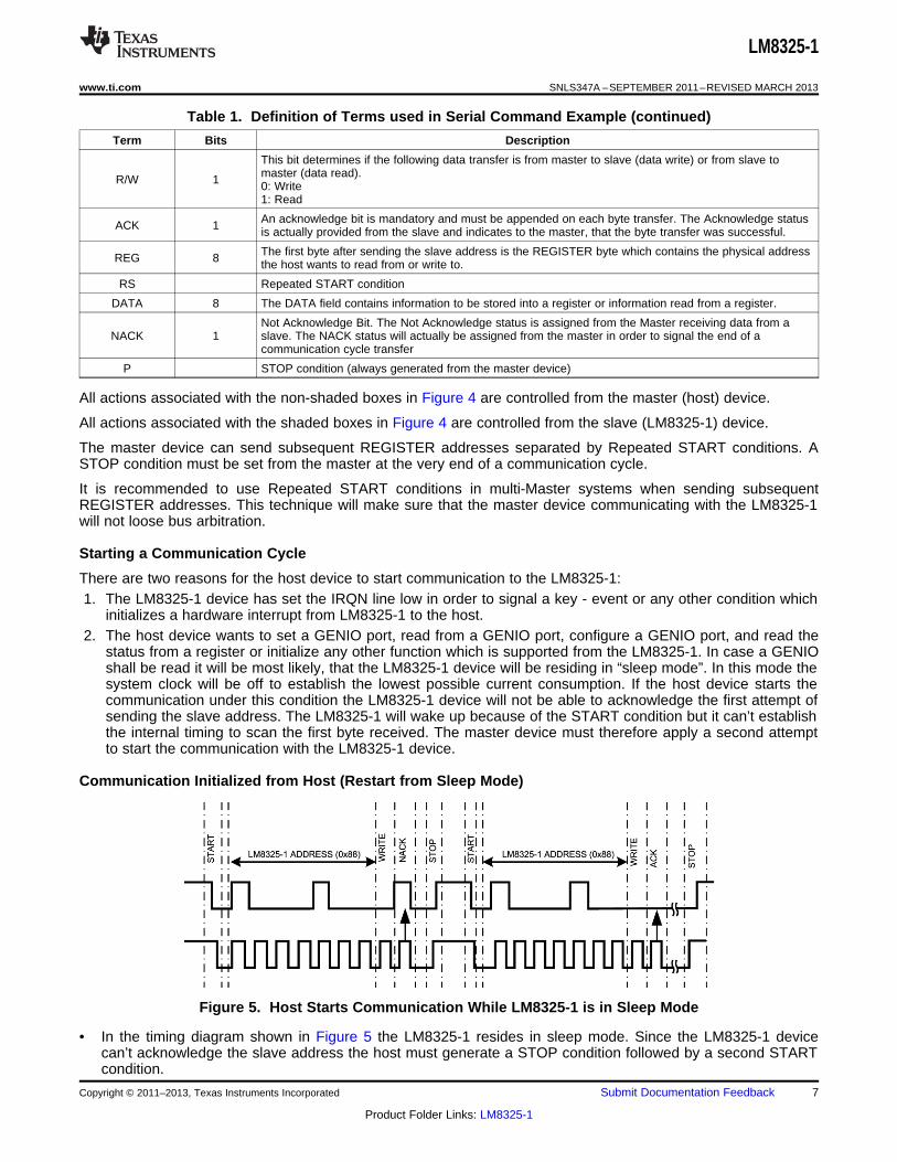
Communication Initialized from Host (Restart from Sleep Mode)
Figure 5. Host Starts Communication While LM8325-1 is in Sleep Mode
• In the timing diagram shown in Figure 5 the LM8325-1 resides in sleep mode. Since the LM8325-1 devicecan’t acknowledge the slave address the host must generate a STOP condition followed by a second STARTcondition.
Copyright © 2011–2013, Texas Instruments Incorporated Submit Documentation Feedback 7
Product Folder Links: LM8325-1

LM8325-1
SNLS347A –SEPTEMBER 2011–REVISED MARCH 2013 www.ti.com
• On the second attempt the slave address is being acknowledged from the LM8325-1 device because it is inactive mode now.
• The host can send different WRITE and/or READ commands subsequently after each other.• The host must finally free the bus by generating a STOP condition.
ACCESS.Bus Communication Flow
The LM8325-1 will only be driven in slave mode. The maximum communication speed supported is Fast Mode(FS) which is 400 kHz. The device can be heavily loaded as it is processing different kind of events caused fromthe human interface and the host device. In such cases the LM8325-1 may temporarily be unable to accept newcommands and data sent from the host device.
NOTE“It is a legitimate measure of the slave device to hold SCL line low in such cases in orderto force the master device into a waiting state!. It is therefore the obligation of the hostdevice to detect such cases. Typically there is a control bit set in the master deviceindicating the Busy status of the bus. As soon as the SCL line is released the host cancontinue sending commands and data.”
Further Remarks:• In systems with multiple masters it is recommended to separate commands with Repeat START conditions
rather than sending a STOP - and another START - condition to communicate with the LM8325-1 device.• Delays enforced by the LM8325-1 during very busy phases of operation should typically not exceed a
duration of 100 usec.• Normally the LM8325-1 will clock stretch after the acknowledge bit Is transmitted; however, there are some
conditions where the LM8325-1 will clock stretch between the SDA Start bit and the first rising edge of SCL.
Auto Increment
In order to improve multi-byte register access, the LM8325-1 supports the auto increment of the address pointer.
A typical protocol access sequence to the LM8325-1 starts with the I2C-compatible ACCESS.bus address,followed by REG, the register to access (see Figure 4). After a REPEATED START condition the hostreads/writes a data byte from/to this address location. If more than one byte is transmitted, the LM8325-1automatically increments the address pointer for each data byte by 1. The address pointer keeps the status untilthe STOP condition is received.
The LM8325-1 always uses auto increments unless otherwise noted.
Please refer to Table 3 and Table 3 for the typical ACCESS.bus flow of reading and writing multiple data bytes.
Reserved Registers and Bits
The LM8325-1 includes reserved registers for future implementation options. Please use value 0 on a write to allreserved register bits.
Global Call Reset
The LM8325-1 supports the Global Call Reset as defined in the I2C Specification, which can be used by the hostto reset all devices connected to interface. The Global call reset is a single byte ACCESS.bus/I2C write of databyte 0x06 to slave address 0x00.
The Global Call Reset changes the I2C-compatible ACCESS.bus Slave address of the LM8325-1 back to itsdefault value of 0x88.
8 Submit Documentation Feedback Copyright © 2011–2013, Texas Instruments Incorporated
Product Folder Links: LM8325-1

LM8325-1
www.ti.com SNLS347A –SEPTEMBER 2011–REVISED MARCH 2013
Table 2. Multi-Byte Write with Auto Increment
Step Master/Slave I2C Com. Value Address Pointer Comment
1 M S START condition
2 M ADDR. 0x88 I2C-compatible ACCESS.bus Address
3 M R/W 0 Write
4 S ACK Acknowledge
5 M REG 0xAA 0xAA Register Address, used as Address Pointer
6 S ACK 0xAA Acknowledge
7 M DATA 0x01 0xAA Write Data to Address in Pointer
8 S ACK 0 0xAB Acknowledge, Address pointer incremented
9 M DATA 0x05 0xAB Write Data to address 0xAB
10 S ACK 0 0xAC Acknowledge, Address pointer incremented
11 M P STOP condition
Table 3. Multi-Byte Read with Auto Increment
Step Master/Slave I2C Com. Value Address Pointer Comment
1 M S START condition
2 M ADDR. 0x88 I2C-compatible ACCESS.bus Address
3 M R/W 0 Write
4 S ACK Acknowledge
5 M REG 0xAA 0xAA Register Address, used as Address pointer
6 S ACK 0xAA Acknowledge
7 M RS 0xAA Repeated Start
8 M ADDR. 0x88 0xAA I2C-compatible ACCESS.bus Address
9 M R/W 1 Read
10 S ACK 0 0xAA Acknowledge
11 S DATA 0x01 0xAA Read Data from Address in Pointer
12 M ACK 0 0xAB Acknowledge, Address Pointer incremented
13 S DATA 0x05 0xAB Read Data from Address in Pointer
14 M NACK 0 0xAC No Acknowledge, stops transmission
15 M P STOP condition
Copyright © 2011–2013, Texas Instruments Incorporated Submit Documentation Feedback 9
Product Folder Links: LM8325-1

LM8325-1
SNLS347A –SEPTEMBER 2011–REVISED MARCH 2013 www.ti.com
KEYSCAN OPERATION
KEYSCAN INITIALIZATION
Figure 6. Keyscan Initialization
KEYSCAN INITIALIZATION EXAMPLE
Table 4 shows all the LM8325-1 register configurations to initialize keyscan:• Keypad matrix configuration is 8 rows x 8 columns.
Table 4. Keyscan Initialization Example
Register name adress Access Type Value Comment
CLKEN 0x8A byte 0x01 enable keyscan clock
KBDSETTLE 0x01 byte 0x80 set the keyscan settle time to 12 msec
KBDBOUNCE 0x02 byte 0x80 set the keyscan debounce time to 12 msec
KBDSIZE 0x03 byte 0x88 set the keyscan matrix size to 8 rows x 8 columns
KBDDEDCFG 0x04 word 0xFC3F configure KPX[7:2] and KPY[7:2] pins as keyboard matrix
IOCFG 0xA7 byte 0xF8 write default value to enable all pins as keyboard matrix
IOPC0 0xAA word 0xAAAA configure pull-up resistors for KPX[7:0]
IOPC1 0xAC word 0x5555 configure pull-down resistors for KPY[7:0]
KBDIC 0x08 byte 0x03 clear any pending interrupts
KBDMSK 0x09 byte 0x03 enable keyboard interrupts
10 Submit Documentation Feedback Copyright © 2011–2013, Texas Instruments Incorporated
Product Folder Links: LM8325-1
LM8325-1
www.ti.com SNLS347A –SEPTEMBER 2011–REVISED MARCH 2013
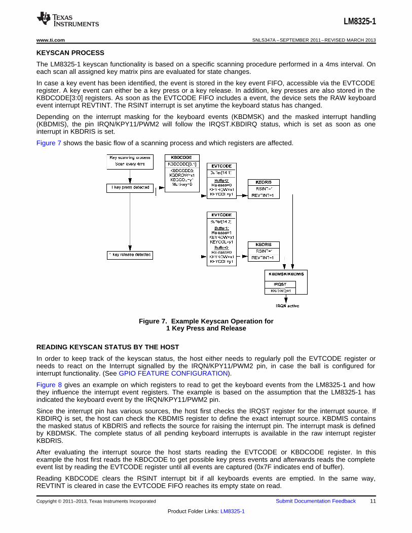
KEYSCAN PROCESS
The LM8325-1 keyscan functionality is based on a specific scanning procedure performed in a 4ms interval. Oneach scan all assigned key matrix pins are evaluated for state changes.
In case a key event has been identified, the event is stored in the key event FIFO, accessible via the EVTCODEregister. A key event can either be a key press or a key release. In addition, key presses are also stored in theKBDCODE[3:0] registers. As soon as the EVTCODE FIFO includes a event, the device sets the RAW keyboardevent interrupt REVTINT. The RSINT interrupt is set anytime the keyboard status has changed.
Depending on the interrupt masking for the keyboard events (KBDMSK) and the masked interrupt handling(KBDMIS), the pin IRQN/KPY11/PWM2 will follow the IRQST.KBDIRQ status, which is set as soon as oneinterrupt in KBDRIS is set.
Figure 7 shows the basic flow of a scanning process and which registers are affected.
Figure 7. Example Keyscan Operation for1 Key Press and Release
READING KEYSCAN STATUS BY THE HOST
In order to keep track of the keyscan status, the host either needs to regularly poll the EVTCODE register orneeds to react on the Interrupt signalled by the IRQN/KPY11/PWM2 pin, in case the ball is configured forinterrupt functionality. (See GPIO FEATURE CONFIGURATION).
Figure 8 gives an example on which registers to read to get the keyboard events from the LM8325-1 and howthey influence the interrupt event registers. The example is based on the assumption that the LM8325-1 hasindicated the keyboard event by the IRQN/KPY11/PWM2 pin.
Since the interrupt pin has various sources, the host first checks the IRQST register for the interrupt source. IfKBDIRQ is set, the host can check the KBDMIS register to define the exact interrupt source. KBDMIS containsthe masked status of KBDRIS and reflects the source for raising the interrupt pin. The interrupt mask is definedby KBDMSK. The complete status of all pending keyboard interrupts is available in the raw interrupt registerKBDRIS.
After evaluating the interrupt source the host starts reading the EVTCODE or KBDCODE register. In thisexample the host first reads the KBDCODE to get possible key press events and afterwards reads the completeevent list by reading the EVTCODE register until all events are captured (0x7F indicates end of buffer).
Reading KBDCODE clears the RSINT interrupt bit if all keyboards events are emptied. In the same way,REVTINT is cleared in case the EVTCODE FIFO reaches its empty state on read.
Copyright © 2011–2013, Texas Instruments Incorporated Submit Documentation Feedback 11
Product Folder Links: LM8325-1

LM8325-1
SNLS347A –SEPTEMBER 2011–REVISED MARCH 2013 www.ti.com
The event buffer content and the REVTINT and RELINT (lost event) interrupt bits are also cleared if theKBDIC.EVTIC bit is set.
Interrupt bits in the masked interrupt register KBDMIS follow the masked KBDRIS status.
In order to support efficient Multi-byte reads from EVTCODE, the autoincrement feature is turned off for thisregister. Therefore the host can continuously read the complete EVTCODE buffer by sending one command.
Figure 8. Example Host Reacting toInterrupt for Keypad Event
MULTIPLE KEY PRESSES
The LM8325-1 supports up to four simultaneous key presses. Any time a single key is pressed KBDCODE0 isset with the appropriate key code. If a second key is pressed, the key is stored in KBDCODE1 and theMULTIKEY flag of KBDCODE0 is set. Additional key presses are stored in KBDCODE2 and KBDCODE3accordingly. The four registers signal the last multi key press events.
All events are stored in parallel in the EVTCODE register for the complete set of events.
All KBDCODE[3:0] registers are cleared on read.
12 Submit Documentation Feedback Copyright © 2011–2013, Texas Instruments Incorporated
Product Folder Links: LM8325-1

LM8325-1
www.ti.com SNLS347A –SEPTEMBER 2011–REVISED MARCH 2013
Figure 9. Example Keyscan Operation for 2 Key Press Eventsand 1 Key Release Event
PWM TIMER
The LM8325-1 supports a timer module dedicated to smooth LED control techniques (lighting controls).
The PWM timer module consists of three independent timer units of which each can generate a PWM output witha fixed period and automatically incrementing or decrementing variable duty cycle. The timer units are all clockedwith a slow (32.768 kHz) clock whereas the interface operates with the main system clock.
OVERVIEW OF PWM FEATURES• Each PWM can establish fixed — or variable — duty-cycle signal sequences on its output.• Each PWM can trigger execution of any pre-programmed task on another PWM channel.• The execution of any pre-programmed task is self-sustaining and does not require further interaction from the
host.• 64-byte script buffer for each PWM for up to 32 consecutive instructions.• Direct addressing within script buffer to support multiple PWM tasks in one buffer.
OVERVIEW ON PWM SCRIPT COMMANDS
The commands listed in Table 5 are dedicated to the slow PWM timers.
NOTEThe PWM Script commands are not part of the command set supported by the LM8325-1command interpreter. These commands must be transferred from the host with help of theregister-based command set.
Copyright © 2011–2013, Texas Instruments Incorporated Submit Documentation Feedback 13
Product Folder Links: LM8325-1

LM8325-1
SNLS347A –SEPTEMBER 2011–REVISED MARCH 2013 www.ti.com
Table 5. PWM Script CommandsCommand 15 14 13 12 11 10 9 8 7 6 5 4 3 2 1 0
RAMP 0 PRESCALE STEPTIME SIGN INCREMENT
SET_PWM 0 1 0 PWMVALUE
GO_TO_0
START
BRANCH 1 0 1 LOOPCOUNT ADDR STEPNUMBER
END 1 1 0 1 INT X
TRIGGER 1 1 1 WAITTRIGGER SENDTRIGGER 0
RAMP COMMAND
A RAMP command will vary the duty cycle of a PWM output in either direction (up or down). The INCREMENTfield specifies the amount of steps for the RAMP. The maximum amount of steps which can be executed withone RAMP Command is 126 which is equivalent to 50%. The SIGN bit field determines the direction of a RAMP(up or down). The STEPTIME field and the PRESCALE bit determine the duration of one step. Based on a32.768 kHz clock, the minimum time resulting from these options would be 0.49 milliseconds and the maximumtime for one step would be 1 second.
Table 6. RAMP Command Bit and Building Fields15 14 13 12 11 10 9 8 7 6 5 4 3 2 1 0
0 PRESCALE STEPTIME SIGN INCREMENT
Table 7. Description of Bit and Building Fields of the RAMP Command
Bit or Field Value Description
0 Divide the 32.768 kHz clock by 16PRESCALE
1 Divide the 32.768 kHz clock by 512
STEPTIME 1 - 63 Number of prescaled clock cycles per step
0 Increment RAMPcounterSIGN
1 Decrement RAMPcounter
Number of steps executed by this instruction; a value of 0 functions as a WAITINCREMENT 0 - 126 determined by STEPTIME.
SET_PWM COMMAND
The SET_PWM command will set the starting duty cycle MIN SCALE or FULL SCALE (0% or 100%). A RAMPcommand following the SET_PWM command will finally establish the desired duty cycle on the PWM output.
Table 8. SET_PWM Command Bit and Building Fields15 14 13 12 11 10 9 8 7 6 5 4 3 2 1 0
0 1 0 0 0 0 0 0 DUTYCYCLE
Table 9. Description of Bit and Building Fields of the SET_PWM Command
Bit or Field Value Description
0 Duty cycle is 0%.DUTYCYCLE
255 Duty cycle is 100%.
GO_TO_START COMMAND
The GO_TO_START command jumps to the first command in the script command file.
14 Submit Documentation Feedback Copyright © 2011–2013, Texas Instruments Incorporated
Product Folder Links: LM8325-1

LM8325-1
www.ti.com SNLS347A –SEPTEMBER 2011–REVISED MARCH 2013
Table 10. GO_TO_START Command Bit and Building Fields15 14 13 12 11 10 9 8 7 6 5 4 3 2 1 0
0
BRANCH COMMAND
The BRANCH command jumps to the specified command in the script command file. The branch is executedwith either absolute or relative addressing. In addition, the command gives the option of looping for a specifiednumber of repetitions.
NOTENested loops are not allowed.
Table 11. BRANCH Command Bit and Building Fields15 14 13 12 11 10 9 8 7 6 5 4 3 2 1 0
1 0 1 LOOPCOUNT ADDR STEPNUMBER
Table 12. Description of Bit and Building Fields of the BRANCH Command
Bit or Field Value Description
0 Loop until a STOP PWM SCRIPT command is issued by the host.LOOPCOUNT
1 - 63 Number of loops to perform.
0 Absolute addressingADDR
1 Relative addressing
Depending on ADDR:STEPNUMBER 0 - 63 ADDR = 0; Addr to jump to
ADDR = 1 - Number of backward steps
TRIGGER COMMAND
Triggers are used to synchronize operations between PWM channels. A TRIGGER command that sends atrigger takes sixteen 32.768 kHz clock cycles, and a command that waits for a trigger takes at least sixteen32.768 kHz clock cycles.
A TRIGGER command that waits for a trigger (or triggers) will stall script execution until the trigger conditions aresatisfied. On trigger it will clear the trigger(s) and continue to the next command.
When a trigger is sent, it is stored by the receiving channel and can only be cleared when the receiving channelexecutes a TRIGGER command that waits for the trigger.
Table 13. TRIGGER Command Bit and Building Fields15 14 13 12 11 10 9 8 7 6 5 4 3 2 1 0
1 1 1 WAITTRIGGER SENDTRIGGER 0
Table 14. Description of Bit and Building Fields
Field Value Description
000xx1 Wait for trigger from channel 0
WAITTRIGGER 000x1x Wait for trigger from channel 1
0001xx Wait for trigger from channel 2
000xx1 Send trigger to channel 0
SENDTRIGGER 000x1x Send trigger to channel 1
0001xx Send trigger to channel 2
Copyright © 2011–2013, Texas Instruments Incorporated Submit Documentation Feedback 15
Product Folder Links: LM8325-1

LM8325-1
SNLS347A –SEPTEMBER 2011–REVISED MARCH 2013 www.ti.com
END COMMAND
The END command terminates script execution. It will only assert an interrupt to the host if the INT bit is set to“1”.
When the END command is executed, the PWM output will be set to the level defined by PWMCFG.PWMPOLfor this channel. Also, the script counter is reset back to the beginning of the script command buffer.
NOTEIf a PWM channel is waiting for the trigger (last executed command was "TRIGGER") andthe script execution is halted then the "END" command can’t be executed because theprevious command is still pending. This is an exception - in this case the IRQ signal willnot be asserted.
Table 15. END Command Bit and Building Fields15 14 13 12 11 10 9 8 7 6 5 4 3 2 1 0
1 1 0 1 INT 0
Table 16. Description of Bit and Building Fields of the END Command
Field Value Description
0 No interrupt will be sent.INT
1 Set TIMRIS.CDIRQ for this PWM channel to notify that program has ended.
LM8325-1 REGISTER SET
KEYBOARD REGISTERS AND KEYBOARD CONTROL
Keyboard selection and control registers are mapped in the address range from 0x01 to 0x10. This paragraphdescribes the functions of the associated registers down to the bit level.
KBDSETTLE - Keypad Settle Time Register
Table 17. KBDSETTLE - Keypad Settle Time Register
Register - Name Address Type Register Function
KBDSETTLE 0x01 R/W Initial time for keys to settle, before the key-scan process is started.
Bit - Name Bit Default Bit Function
The default value 0x80 : 0xBF sets a time target of 12 msec
Further time targets are as follows:
0xC0 - 0xFF: 16 msec
WAIT[7:0] 7:0 0x80 0x80 - 0xBF: 12 msec
0x40 - 0x7F: 8 msec
0x01 - 0x3F: 4 msec
0x00 : no settle time
KBDBOUNCE - Debounce Time Register
Table 18. KBDBOUNCE - Debounce Time Register
Register - Name Address Type Register Function
KBDBOUNCE 0x02 R/W Time between first detection of key and final sampling of key
Bit - Name Bit Default Bit Function
16 Submit Documentation Feedback Copyright © 2011–2013, Texas Instruments Incorporated
Product Folder Links: LM8325-1

LM8325-1
www.ti.com SNLS347A –SEPTEMBER 2011–REVISED MARCH 2013
Table 18. KBDBOUNCE - Debounce Time Register (continued)
Register - Name Address Type Register Function
The default value 0x80 : 0xBF sets a time target of 12 msec
Further time targets are as follows:
0xC0 - 0xFF: 16 msec
WAIT[7:0] 7:0 0x80 0x80 - 0xBF: 12 msec
0x40 - 0x7F: 8 msec
0x01 - 0x3F: 4 msec
0x00: no debouncing time
KBDSIZE - Set Keypad Size Register
Table 19. KBDSIZE - Set Keypad Size Register
Register - Name Address Type Register Function
KBDSIZE 0x03 R/W Defines the physical keyboard matrix size
Bit - Name Bit Default Bit Function
Number of rows in the keyboard matrix
0x0: free all rows to become GPIO, KPX[1:0] used as dedicated key inputsif scanning is enabled by CLKEN.KBENROWSIZE[3:0] 7:4 0x20x1: (illegal value)
0x2 - 0x8: Number of rows in the matrix
Number of columns in the keyboard matrix
0x0: free all rows to become GPIO, KPY[1:0] used as dedicated key inputsif scanning is enabled by CLKEN.KBENCOLSIZE[3:0] 3:0 0x20x1: (illegal value)
0x2 - 0xC: Number of columns in the matrix
KBDDEDCFG - Dedicated Key Register
Table 20. KBDDEDCFG - Dedicated Key Register
Register - Name Address Type Register Function
Defines if a key is used as a standard keyboard/GPIO pin or whether it isKBDDEDCFG 0x04 R/W used as dedicated key input.
Bit - Name Bit Default Bit Function
Each bit in ROW [7:2] corresponds to ball KPX7 : KPX2.
Bit=0: the dedicated key function applies.ROW[7:2] 15:10 0x3F Bit=1: no dedicated key function is selected. The standard GPIO
functionality applies according to register IOCFG or defined keyboardmatrix.
Each bit in COL [11:10] corresponds to ball KPY11 : KPY10.
Bit=0: the dedicated key function applies.COL[11:10] 9:8 0x03 Bit=1: no dedicated key function is selected. The standard GPIO
functionality applies according to register IOCFG or defined keyboardmatrix.
Each bit in COL [9:2] corresponds to ball KPY9 : KPY2 and can beconfigured individually.
Bit=0: the dedicated key function applies.COL[9:2] 7:0 0xFFBit=1: no dedicated key function is selected. The standard GPIOfunctionality applies according to register IOCFG or defined keyboardmatrix.
Copyright © 2011–2013, Texas Instruments Incorporated Submit Documentation Feedback 17
Product Folder Links: LM8325-1

LM8325-1
SNLS347A –SEPTEMBER 2011–REVISED MARCH 2013 www.ti.com
KBDRIS - Keyboard Raw Interrupt Status Register
Table 21. KBDRIS - Keyboard Raw Interrupt Status Register
Register - Name Address Type Register Function
KBDRIS 0x06 R Returns the status of stored keyboard interrupts.
Bit - Name Bit Default Bit Function
(reserved) 7:4 (reserved)
Raw event lost interrupt.
More than 8 keyboard events have been detected and caused the eventRELINT 3 0x0buffer to overflow. This bit is cleared by setting bit EVTIC of the KBDICregister.
Raw keyboard event interrupt.REVTINT 2 0x0 At least one key press or key release is in the keyboard event buffer.
Reading from EVTCODE until the buffer is empty will clear this interrupt.
Raw key lost interrupt indicates a lost key-code.
This interrupt is asserted when RSINT has not been cleared uponRKLINT 1 0x0detection of a new key press or key release, or when more than 4 keysare pressed simultaneously.
Raw scan interrupt.RSINT 0 0x0 Interrupt generated after keyboard scan, if the keyboard status has
changed.
KBDMIS - Keypad Masked Interrupt Status Register
Table 22. KBDMIS - Keypad Masked Interrupt Status Register
Register - Name Address Type Register Function
Returns the status on masked keyboard interrupts after masking with theKBDMIS 0x07 R KBDMSK register.
Bit - Name Bit Default Bit Functions
(reserved) 7:4 (reserved)
Masked event lost interrupt.
More than 8 keyboard events have been detected and caused the eventMELINT 3 0x0buffer to overflow. This bit is cleared by setting bit EVTIC of the KBDICregister.
Masked keyboard event interrupt.MEVTINT 2 0x0 At least one key press or key release is in the keyboard event buffer.
Reading from EVTCODE until the buffer is empty will clear this interrupt.
Masked key lost interrupt.
Indicates a lost key-code. This interrupt is asserted when RSINT has notMKLINT 1 0x0been cleared upon detection of a new key press or key release, or whenmore than 4 keys are pressed simultaneously.
Masked scan interrupt.MSINT 0 0x0 Interrupt generated after keyboard scan, if the keyboard status has
changed, after masking process.
KBDIC - Keypad Interrupt Clear Register
Table 23. KBDIC - Keypad Interrupt Clear Register
Register - Name Address Default Register Function
KBDIC 0x08 W Setting these bits clears Keypad active Interrupts
Bit - Name Bit Default Bit Function
18 Submit Documentation Feedback Copyright © 2011–2013, Texas Instruments Incorporated
Product Folder Links: LM8325-1

LM8325-1
www.ti.com SNLS347A –SEPTEMBER 2011–REVISED MARCH 2013
Table 23. KBDIC - Keypad Interrupt Clear Register (continued)
Register - Name Address Default Register Function
Switches off scanning of special function (SF) keys, when keyboard hasno special function layout.
SFOFF 7 0: keyboard layout and SF keys are scanned
1: only keyboard layout is scanned, SF keys are not scanned
(reserved) 6:2 (reserved)
Clear event buffer and corresponding interrupts REVTINT and RELINT byEVTIC 1 writing a 1 to this bit position
KBDIC 0 Clear RSINT and RKLINT interrupt bits by writing a 1 to this bit position.
KBDMSK - Keypad Interrupt Mask Register
Table 24. KBDMSK - Keypad Interrupt Mask Register
Register - Name Address Type Register Function
Configures masking of keyboard interrupts. Masked interrupts do nottrigger an event on the Interrupt output.
In case the interrupt processes registers KBDCODE[3:0], MSKELINT andKBDMSK 0x09 R/W MSKEINT should be set to 1. When the Event FIFO is processed,
MSKLINT and MSKSINT should be set. For keyboard polling operations,all bits should be set and the polling operation consists of reading out theEVTCODE.
Bit - Name Bit Default Bit Function
(reserved) 7:4 (reserved)
0: keyboard event lost interrupt RELINT triggers IRQ lineMSKELINT 3 0x0
1: keyboard event lost interrupt RELINT is masked
0: keyboard event interrupt REVINT triggers IRQ lineMSKEINT 2 0x0
1: keyboard event interrupt REVINT is masked
0: keyboard lost interrupt RKLINT triggers IRQ lineMSKLINT 1 0x1
1: keyboard lost interrupt RKLINT is masked
0: keyboard status interrupt RSINT triggers IRQ lineMSKSINT 0 0x1
1: keyboard status interrupt RSINT is masked
KBDCODE0 - Keyboard Code Register 0
The key code detected by the keyboard scan can be read from the registers KBDCODE0: KBDCODE3. Up to 4keys can be detected simultaneously. Each KBDCODE register includes a bit (MULTIKEY) indicating if anotherkey has been detected.
NOTEReading out all key code registers (KBDCODE0 to KBDCODE3) will automatically resetthe keyboard scan interrupt RSINT the same way as an active write access into bit KBDICof the interrupt clear register does. Reading 0x7F from the KBDCODE0 register meansthat no key was pressed.
Table 25. KBDCODE0 - Keyboard Code Register 0
Register - Name Address Default Register Function
KBDCODE0 0x0B R Holds the row and column information of the first detected key
Bit - Name Bit Default Bit Function
MULTIKEY 7 0x0 if this bit is 1 another key is available in KBDCODE1 register
KEYROW[2:0] 6:4 0x7 ROW index of detected key (0 to 7)
KEYCOL[3:0] 3:0 0xF Column index of detected (0 to 11, 12 for special function key.
Copyright © 2011–2013, Texas Instruments Incorporated Submit Documentation Feedback 19
Product Folder Links: LM8325-1

LM8325-1
SNLS347A –SEPTEMBER 2011–REVISED MARCH 2013 www.ti.com
KBDCODE1 - Keyboard Code Register 1
Table 26. KBDCODE1 - Keyboard Code Register 1
Register - Name Address Default Register Function
KBDCODE1 0x0C R Holds the row and column information of the second detected key
Bit - Name Bit Default Bit Function
MULTIKEY 7 0x0 if this bit is 1 another key is available in KBDCODE2 register
KEYROW[2:0] 6:4 0x7 ROW index of detected key (0 to 7)
KEYCOL[3:0] 3:0 0xF Column index of detected key (0 to 11, 12 for special function key.
KBDCODE2 - Keyboard Code Register 2
Table 27. KBDCODE2 - Keyboard Code Register 2
Register - Name Address Default Register Function
KBDCODE2 0x0D R Holds the row and column information of the third detected key
Bit - Name Bit Default Bit Function
MULTIKEY 7 0x0 if this bit is 1 another key is available in KBDCODE3 register
KEYROW[2:0] 6:4 0x7 ROW index of detected key (0 to 7)
KEYCOL[3:0] 3:0 0xF Column index of detected key (0 to 11, 12 for special function key.
KBDCODE3 - Keyboard Code Register 3
Table 28. KBDCODE3 - Keyboard Code Register 3
Register - Name Address Default Register Function
KBDCODE3 0x0E R Holds the row and column information of the forth detected key
Bit - Name Bit Default Bit Function
MULTIKEY 7 0x0 if this bit is set to “1” then more than 4 keys are pressed simultaneously.
KEYROW[2:0] 6:4 0x7 ROW index of detected key (0 to 7)
KEYCOL[3:0] 3:0 0xF Column index of detected key (0 to 11, 12 for special function key.
EVTCODE - Key Event Code Register
Table 29. EVTCODE - Key Event Code Register
Register - Name Address Default Bit Function
With this register a FIFO buffer is addressed storing up to 15 consecutiveevents.
Reading the value 0x7F from this address means that the FIFO buffer isEVTCODE 0x10 R empty. See further details below.
NOTE: Auto increment is disabled on this register. Multi-byte read willalways read from the same address.
Bit - Name Bit Default Bit Function
This bit indicates, whether the keyboard event was a key press or a keyrelease event.
RELEASE 7 0x0 0: key was pressed
1: key was released
KEYROW[2:0] 6:4 0x7 Row index of key that is pressed or released.
Column index of key that is pressed (0...11, 12 for special function key) orKEYCOL[3:0] 3:0 0xF released.
20 Submit Documentation Feedback Copyright © 2011–2013, Texas Instruments Incorporated
Product Folder Links: LM8325-1

LM8325-1
www.ti.com SNLS347A –SEPTEMBER 2011–REVISED MARCH 2013
PWM TIMER CONTROL REGISTERS
The LM8325-1 provides three host-programmable PWM outputs useful for smooth LED brightness modulation.All PWM timer control registers are mapped in the range from 0x60 to 0x7F. This paragraph describes thefunctions of the associated registers down to the bit level.
TIMCFGx - PWM Timer 0, 1 and 2 Configuration Registers
Table 30. TIMCFGx - PWM Timer 0, 1 and 2 Configuration Registers
Register - Name Address Type Register Function
TIMCFG0 0x60This register configures interrupt masking and handles PWM start/stopTIMCFG1 0x68 R/W control of the associated PWM channel.
TIMCFG2 0x70
Bit - Name Bit Default Bit Function(x = 0, 1 or 2)
Interrupt mask for PWM CYCIRQx (see register TIMRIS)
CYCIRQxMSK 4 0x0 0: interrupt enabled
1: interrupt masked
(reserved) 3:0 0x0 (reserved)
PWMCFGx - PWM Timer 0, 1 and 2 Configuration Control Registers
Table 31. PWMCFGx - PWM Timer 0, 1 and 2 Configuration Control Registers
Register - Name Address Type Register Function
This register defines interrupt masking and the output behavior for thePWMCFG0 0x61 associated PWM channel.
PWMCFG1 0x69 R/W PGEx is used to start and stop the PWM script execution.
PWMENx sets the PWM output to either reflect the generated pattern orPWMCFG2 0x71 the value configured in PWMPOLx.
Bit - Name Bit Default Bit Function(x = 0, 1 or 2)
Mask for CDIRQx
CDIRQxMSK 3 0x0 0: CDIRQx enabled
1: CDIRQx disabled/masked
Pattern Generator Enable. Start/Stop PWM command processing for thischannel. Script execution is started always from beginning.
PGEx 2 0x0 0: Pattern Generator disabled
1: Pattern Generator enabled
0: PWM disabled. PWM timer output assumes value programmed inPWMPOL.PWMENx 1 0x01: PWM enabled
Off-state of PWM output, when PWMEN=0.
PWMPOLx 0 0x0 0: PWM off-state is low
1: PWM off-state is high
Copyright © 2011–2013, Texas Instruments Incorporated Submit Documentation Feedback 21
Product Folder Links: LM8325-1
LM8325-1
SNLS347A –SEPTEMBER 2011–REVISED MARCH 2013 www.ti.com
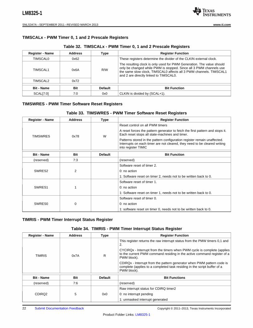
TIMSCALx - PWM Timer 0, 1 and 2 Prescale Registers
Table 32. TIMSCALx - PWM Timer 0, 1 and 2 Prescale Registers
Register - Name Address Type Register Function
TIMSCAL0 0x62 These registers determine the divider of the CLKIN external clock.
The resulting clock is only used for PWM Generation. The value shouldonly be changed while PWM is stopped. Since all 3 PWM channels useTIMSCAL1 0x6A R/W the same slow clock, TIMSCAL0 affects all 3 PWM channels. TIMSCAL1and 2 are directly linked to TIMSCAL0.
TIMSCAL2 0x72
Bit - Name Bit Default Bit Function
SCAL[7:0] 7:0 0x0 CLKIN is divided by (SCAL+1).
TIMSWRES - PWM Timer Software Reset Registers
Table 33. TIMSWRES - PWM Timer Software Reset Registers
Register - Name Address Type Register Function
Reset control on all PWM timers
A reset forces the pattern generator to fetch the first pattern and stops it.Each reset stops all state-machines and timer.TIMSWRES 0x78 WPatterns stored in the pattern configuration register remain unaffected.Interrupts on each timer are not cleared, they need to be cleared writinginto register TIMIC
Bit - Name Bit Default Bit Function
(reserved) 7:3 (reserved)
Software reset of timer 2.
SWRES2 2 0: no action
1: Software reset on timer 2, needs not to be written back to 0.
Software reset of timer 1.
SWRES1 1 0: no action
1: Software reset on timer 1, needs not to be written back to 0.
Software reset of timer 0.
SWRES0 0 0: no action
1: software reset on timer 0, needs not to be written back to 0.
TIMRIS - PWM Timer Interrupt Status Register
Table 34. TIMRIS - PWM Timer Interrupt Status Register
Register - Name Address Type Register Function
This register returns the raw interrupt status from the PMW timers 0,1 and2.
CYCIRQx - Interrupt from the timers when PWM cycle is complete (appliesto the current PWM command residing in the active command register of aTIMRIS 0x7A R PWM block).
CDIRQx - Interrupt from the pattern generator when PWM pattern code iscomplete (applies to a completed task residing in the script buffer of aPWM block).
Bit - Name Bit Default Bit Functions
(reserved) 7:6 (reserved)
Raw interrupt status for CDIRQ timer2
CDIRQ2 5 0x0 0: no interrupt pending
1: unmasked interrupt generated
22 Submit Documentation Feedback Copyright © 2011–2013, Texas Instruments Incorporated
Product Folder Links: LM8325-1

LM8325-1
www.ti.com SNLS347A –SEPTEMBER 2011–REVISED MARCH 2013
Table 34. TIMRIS - PWM Timer Interrupt Status Register (continued)
Register - Name Address Type Register Function
Raw interrupt status for CDIRQ timer1
CDIRQ1 4 0x0 0: no interrupt pending
1: unmasked interrupt generated
Raw interrupt status for CDIRQ timer0
CDIRQ0 3 0x0 0: no interrupt pending
1: unmasked interrupt generated
Raw interrupt status for CYCIRQ timer2
CYCIRQ2 2 0x0 0: no interrupt pending
1: unmasked interrupt generated
Raw interrupt status for CYCIRQ timer1
CYCIRQ1 1 0x0 0: no interrupt pending
1: unmasked interrupt generated
Raw interrupt status for CYCIRQ timer0
CYCIRQ0 0 0x0 0: no interrupt pending
1: unmasked interrupt generated
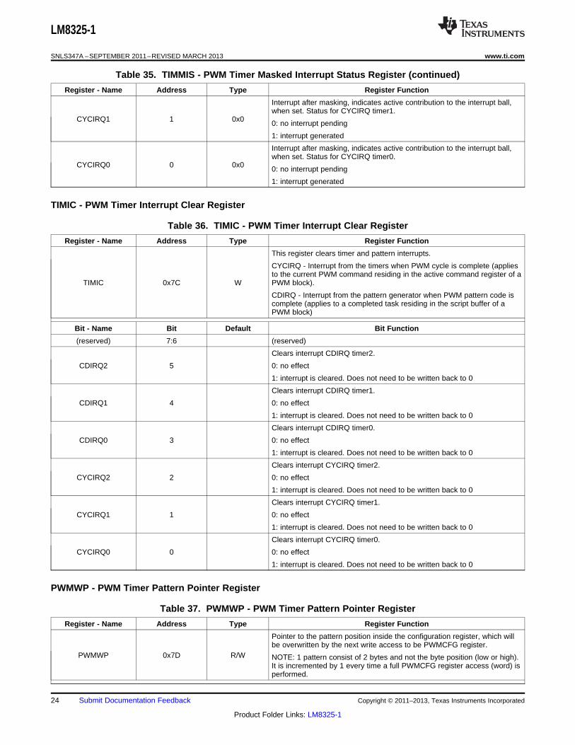
TIMMIS - PWM Timer Masked Interrupt Status Register
Table 35. TIMMIS - PWM Timer Masked Interrupt Status Register
Register - Name Address Type Register Function
This register returns the masked interrupt status from the PMW timers 0,1and 2. The raw interrupt status (TIMRIS) is masked with the associatedTIMCFGx.CYCIRQxMSK and PWMCFGx.CDIRQxMSK bits to get themasked interrupt status of this register.
CYCIRQ - Interrupt from the timers when PWM cycle is complete (appliesTIMMIS 0x7B R to the current PWM command residing in the active command register of aPWM block)
CDIRQ - Interrupt from the pattern generator when PWM pattern code iscomplete (applies to a completed task residing in the script buffer of aPWM block)
Bit - Name Bit Default Bit Function
(reserved) 7:6 (reserved)
Interrupt after masking, indicates active contribution to the interrupt ball,when set. Status for CDIRQ timer2.
CDIRQ2 5 0x0 0: no interrupt pending
1: interrupt generated
Interrupt after masking, indicates active contribution to the interrupt ball,when set. Status for CDIRQ timer1.
CDIRQ1 4 0x0 0: no interrupt pending
1: interrupt generated
Interrupt after masking, indicates active contribution to the interrupt ball,when set. Status for CDIRQ timer0.
CDIRQ0 3 0x0 0: no interrupt pending
1: interrupt generated
Interrupt after masking, indicates active contribution to the interrupt ball,when set. Status for CYCIRQ timer2.
CYCIRQ2 2 0x0 0: no interrupt pending
1: interrupt generated
Copyright © 2011–2013, Texas Instruments Incorporated Submit Documentation Feedback 23
Product Folder Links: LM8325-1
LM8325-1
SNLS347A –SEPTEMBER 2011–REVISED MARCH 2013 www.ti.com
Table 35. TIMMIS - PWM Timer Masked Interrupt Status Register (continued)
Register - Name Address Type Register Function
Interrupt after masking, indicates active contribution to the interrupt ball,when set. Status for CYCIRQ timer1.
CYCIRQ1 1 0x0 0: no interrupt pending
1: interrupt generated
Interrupt after masking, indicates active contribution to the interrupt ball,when set. Status for CYCIRQ timer0.
CYCIRQ0 0 0x0 0: no interrupt pending
1: interrupt generated
TIMIC - PWM Timer Interrupt Clear Register
Table 36. TIMIC - PWM Timer Interrupt Clear Register
Register - Name Address Type Register Function
This register clears timer and pattern interrupts.
CYCIRQ - Interrupt from the timers when PWM cycle is complete (appliesto the current PWM command residing in the active command register of a
TIMIC 0x7C W PWM block).
CDIRQ - Interrupt from the pattern generator when PWM pattern code iscomplete (applies to a completed task residing in the script buffer of aPWM block)
Bit - Name Bit Default Bit Function
(reserved) 7:6 (reserved)
Clears interrupt CDIRQ timer2.
CDIRQ2 5 0: no effect
1: interrupt is cleared. Does not need to be written back to 0
Clears interrupt CDIRQ timer1.
CDIRQ1 4 0: no effect
1: interrupt is cleared. Does not need to be written back to 0
Clears interrupt CDIRQ timer0.
CDIRQ0 3 0: no effect
1: interrupt is cleared. Does not need to be written back to 0
Clears interrupt CYCIRQ timer2.
CYCIRQ2 2 0: no effect
1: interrupt is cleared. Does not need to be written back to 0
Clears interrupt CYCIRQ timer1.
CYCIRQ1 1 0: no effect
1: interrupt is cleared. Does not need to be written back to 0
Clears interrupt CYCIRQ timer0.
CYCIRQ0 0 0: no effect
1: interrupt is cleared. Does not need to be written back to 0
PWMWP - PWM Timer Pattern Pointer Register
Table 37. PWMWP - PWM Timer Pattern Pointer Register
Register - Name Address Type Register Function
Pointer to the pattern position inside the configuration register, which willbe overwritten by the next write access to be PWMCFG register.
PWMWP 0x7D R/W NOTE: 1 pattern consist of 2 bytes and not the byte position (low or high).It is incremented by 1 every time a full PWMCFG register access (word) isperformed.
24 Submit Documentation Feedback Copyright © 2011–2013, Texas Instruments Incorporated
Product Folder Links: LM8325-1

LM8325-1
www.ti.com SNLS347A –SEPTEMBER 2011–REVISED MARCH 2013
Table 37. PWMWP - PWM Timer Pattern Pointer Register (continued)
Register - Name Address Type Register Function
Bit - Name Bit Default Bit Function
(reserved) 7 0x0 (reserved)
0 ≤ POINTER < 32 : timer0 patterns 0 to 31
32 ≤ POINTER < 64 : timer1 patterns 0 to 31POINTER[6:0] 6:0 0x0
64 ≤ POINTER < 96 : timer2 patterns 0 to 31
96 ≤ POINTER < 128: not valid
PWMCFG - PWM Script Register
Table 38. PWMCFG - PWM Script Register
Register - Name Address Type Register Function
Two byte pattern storage register for a PWM script command indexed byPWMWP. PWMWP is automatically incremented.
To be applied by two consecutive parameter bytes in one I2C WriteTransaction.PWMCFG 0x7E WNOTE:
Autoincrement is disabled on this register. Address will stay at 0x7E foreach word access.
Bit - Name Bit Default Bit Function
CMD[15:8] 15:8 High byte portion of a PWM script command
CMD[7:0] 7:0 Low byte portion of a PWM script command
INTERFACE CONTROL REGISTERS
The following section describes the functions of special control registers provided for the main controller.
The manufacturer code MFGCODE and the software revision number SWREV tell the main device whichconfiguration file has to be used for this device.
NOTEI2CSA and MFGCODE use the same address. They just differentiate in the access type:
• Write - I2CSA• Read - MFGCODE
I2CSA - I2C-Compatible ACCESS.bus Slave Address Register
Table 39. I2CSA - I2C-Compatible ACCESS.bus Slave Address Register
Register - Name Address Type Register Function
I2C-compatible ACCESS.bus Slave Address.I2CSA 0x80 W
The address is internally applied after the next I2C STOP.
Bit - Name Bit Default Bit Function
SLAVEADDR[7:1] 7:1 0x44 7-bit address field for the I2C-compatible ACCESS.bus slave address.
(reserved) 0 (reserved)
MFGCODE - Manufacturer Code Register
Table 40. MFGCODE - Manufacturer Code Register
Register - Name Address Type Register Function
MFGCODE 0x80 R Manufacturer code of the LM8325-1
Copyright © 2011–2013, Texas Instruments Incorporated Submit Documentation Feedback 25
Product Folder Links: LM8325-1

LM8325-1
SNLS347A –SEPTEMBER 2011–REVISED MARCH 2013 www.ti.com
Table 40. MFGCODE - Manufacturer Code Register (continued)
Register - Name Address Type Register Function
Bit - Name Bit Default Bit Function
MFGBIT 7:0 0x00 8 - bit field containing the manufacturer code
SWREV - Software Revision Register
Table 41. SWREV - Software Revision Register
Register - Name Address Type Register Function
Software revision code of the LM8325-1.SWREV 0x81 R NOTE: writing the SW revision with the inverted value triggers a reset (see
SWRESET)
Bit - Name Bit Default Bit Function
SWBIT 7:0 0x84 8 - bit field containing the SW Revision number.
SWRESET - Software Reset
Table 42. SWRESET - Software Reset Register
Register - Name Address Type Register Function
Software reset
NOTE: the reset is only applied if the supplied parameter has the invertedSWRESET 0x81 W value as SWBIT.
Reading this register provides the software revision. (see SWREV)
Bit - Name Bit Default Bit Function
SWBIT 7:0 Reapply inverted value for software reset.
RSTCTRL - System Reset Register
This register allows to reset specific blocks of the LM8325-1. For global reset of the IOExpander the I2Ccommand 'General Call reset' is used (see Global Call Reset). This will reset the slave address back to 88H.During an active reset of a module, the LM8325-1 blocks the access to the module registers. A read will return 0,write commands are ignored.
Table 43. RSTCTRL - System Reset Register
Register - Name Address Type Register Function
RSTCTRL 0x82 R/W Software reset of specific parts of the LM8325-1
Bit - Name Bit Default Bit Function
(reserved) 7:5 (reserved)
Interrupt controller reset. Does not change status on IRQN ball. Onlycontrols IRQ module register. Interrupt status read out is not possiblewhen this bit is set.IRQRST 4 0x00: interrupt controller not reset
1: interrupt controller reset
Timer reset for Timers 0, 1, 2
TIMRST 3 0x0 0: timer not reset
1: timer is reset
(reserved) 2 0x0 (reserved)
Keyboard interface reset
KBDRST 1 0x0 0: keyboard is not reset
1: keyboard is reset
26 Submit Documentation Feedback Copyright © 2011–2013, Texas Instruments Incorporated
Product Folder Links: LM8325-1

LM8325-1
www.ti.com SNLS347A –SEPTEMBER 2011–REVISED MARCH 2013
Table 43. RSTCTRL - System Reset Register (continued)
Register - Name Address Type Register Function
GENIO reset
GPIRST 0 0x0 0: GENIO not reset
1: GENIO is reset.
RSTINTCLR - Clear NO Init/Power-On Interrupt Register
Table 44. RSTINTCLR - Clear NO Init/Power-On Interrupt Register
Register - Name Address Type Register Function
This register allows to de-assert the POR/No Init Interrupt set every timeRSTINTCLR 0x84 W the device returns from RESET (either POR, HW or SW Reset), the IRQN
line is assigned active (low) and the IRQST.PORIRQ bit is set.
Bit - Name Bit Default Bit Function
reserved 7:1 (reserved)
1: Clears the PORIRQ Interrupt signalled in IRQST register.IRQCLR 0
0: is ignored
CLKMODE - Clock Mode Register
Table 45. CLKMODE - Clock Mode Register
Register - Name Address Type Register Function
CLKMODE 0x88 R/W This register controls the current operating mode of the LM8325-1 device
Bit - Name Bit Default Bit Function
(reserved) 7:2 (reserved)
Writing to 00 forces the device to immediately enter sleep mode,regardless of any autosleep configuration. Reading this bit returns thecurrent operating mode, which should always be 01.
MODCTL[1:0] 1:0 0x01 00: SLEEP Mode
01: Operation Mode
1x: Future modes
CLKCFG - Clock Configuration Register
Table 46. CLKCFG - Clock Configuration Register
Register - Name Address Type Register Function
Configures clock sources and power options of the device.CLKCFG 0x89 R/W
Note: Don't change while a PWM script is in progress
Bit - Name Bit Default Bit Function
(reserved) 7 0x0 (reserved)
00: (reserved)
CLKSRCSEL[1:0] 6:5 0x2 01: use external generated clock from CLKIN pin as PWM slow clock
1x: use internally generated PWM slow clock
(reserved) 4:0 0x00 (reserved)
CLKEN - Clock Enable Register
Table 47. CLKEN - Clock Enable Register
Register - Name Address Type Register Function
Controls the clock to different functional units. It shall be used to enableCLKEN 0x8A R/W the functional blocks globally and independently.
Copyright © 2011–2013, Texas Instruments Incorporated Submit Documentation Feedback 27
Product Folder Links: LM8325-1

LM8325-1
SNLS347A –SEPTEMBER 2011–REVISED MARCH 2013 www.ti.com
Table 47. CLKEN - Clock Enable Register (continued)
Register - Name Address Type Register Function
Bit - Name Bit Default Bit Function
(reserved) 7:3 (reserved)
PWM Timer 0, 1, 2 clock enable
TIMEN 2 0x0 0: Timer 0, 1, 2 clock disabled
1: Timer 0, 1, 2 clock enabled.
(reserved) 1 (reserved)
Keyboard clock enable (starts/stops key scan)
KBDEN 0 0x0 0: Keyboard clock disabled
1: Keyboard clock enabled
AUTOSLP - Autosleep Enable Register
Table 48. AUTOSLP - Autosleep Enable Register
Register - Name Address Type Register Function
AUTOSLP 0x8B R/W This register controls the Auto Sleep function of the LM8325-1 device
Bit - Name Bit Default Bit Function
(reserved) 7:1 (reserved)
Enables automatic sleep mode after a defined activity time stored in theAUTOSLPTI register
ENABLE 0 0x00 1: Enable entering auto sleep mode
0: Disable entering auto sleep mode
AUTOSLPTI - Auto Sleep Time Register
Table 49. AUTOSLPTI - Auto Sleep Time Register
Register - Name Address Type Register Function
This register defines the activity time. If this time passes without anyAUTOSLPTIL 0x8C R/W processing events then the device enters into sleep-mode, but only ifAUTOSLPTIH 0x8D AUTOSLP.ENABLE bit is set to 1.
Bit - Name Bit Default Bit Function
(reserved) 15:11 (reserved)
Values of UPTIME[10:0] match to multiples of 4ms:0x00: no autosleep, regardless if AUTOSLP.ENABLE is set0x01: 4ms
UPTIME[10:8] 10:8 0x00 0x02: 8msUPTIME[7:0] 7:0 0xFF 0x7A: 500 ms
0xFF: 1020 ms (default after reset)0x100: 1024 ms0x7FF: 8188 ms
IRQST - Global Interrupt Status Register
Table 50. IRQST - Global Interrupt Status Register
Register - Name Address Type Register Function
Returns the interrupt status from various on-chip function blocks. If any ofIRQST 0x91 R the bits is set and an IRQN line is configured, the IRQN line is asserted
active
Bit - Name Bit Default Bit Function
28 Submit Documentation Feedback Copyright © 2011–2013, Texas Instruments Incorporated
Product Folder Links: LM8325-1

LM8325-1
www.ti.com SNLS347A –SEPTEMBER 2011–REVISED MARCH 2013
Table 50. IRQST - Global Interrupt Status Register (continued)
Register - Name Address Type Register Function
Supply failure on VCC.
Also power-on is considered as an initial supply failure. Therefore, afterpower-on, the bit is set.PORIRQ 7 0x10: no failure recorded
1: Failure, device was completely reset and requires re-programming.
Keyboard interrupt (further key selection in keyboard module)
KBDIRQ 6 0x0 0: inactive
1: active
(reserved) 5:4 (reserved)
Timer2 expiry (CDIRQ or CYCIRQ)
TIM2IRQ 3 0x0 0: inactive
1: active
Timer1 expiry (CDIRQ or CYCIRQ)
TIM1IRQ 2 0x0 0: inactive
1: active
Timer0 expiry (CDIRQ or CYCIRQ)
TIM0IRQ 1 0x0 0: inactive
1: active
GPIO interrupt (further selection in GPIO module)
GPIOIRQ 0 0x0 0: inactive
1: active
GPIO FEATURE CONFIGURATION
GPIO Feature Mapping
The LM8325-1 has a flexible IO structure which allows to dynamically assign different functionality to each ball.The functionality of each ball is determined by the complete configuration of the balls.
In general the following priority is given:• Keypad• GPIO/PWM/Interrupt
With this, each ball will be available as GPIO, PWM or interrupt unless it is specified to be part of the keypadmatrix. The configuration for keypad or PWM/interrupt usage is defined by the following registers:• KBDSIZE and KBDDEDCFG
– Both registers define a ball as either part of the keypad matrix or as dedicated key input. These settingshave highest priority and will overwrite settings made in other registers.
• IOCFG– This register is used to define the usage of KPY[11:8] if not configured to be part of the keymatrix, to be
used as GPIO.
Table 51. Ball Configuration Options
BALL Module connectivity
GPIOSEL BALLCFG
0x0 0x1 0x2 0x3 0x4 0x5 0x6 0x7
KPX[7:0] not used GPIO[7:0]
KPY[7:0] not used GPIO[15:8]
KPY8/PWM2 not used GPIO16 PWM2 (1) (reserved) - - - - -
(1) Note 1: PWM2 functionality is mutally exclusive — one pin at a time only (KPY8 or KPY11) depending on interrupt enable Bit 4 ofIOCFG.
Copyright © 2011–2013, Texas Instruments Incorporated Submit Documentation Feedback 29
Product Folder Links: LM8325-1

LM8325-1
SNLS347A –SEPTEMBER 2011–REVISED MARCH 2013 www.ti.com
Table 51. Ball Configuration Options (continued)
BALL Module connectivity
KPY9/PWM1 not used GPIO17 PWM1 - - - - - -
KPY10/PWM0 not used GPIO18 PWM0 - - - - - -
IRQN/KPY11/PW see IOCFG GPIO19 PWM2 (1) PWM2 - - - - -M2
IOCGF - Input/Output Pin Mapping Configuration Register
Table 52. IOCGF - Input/Output Pin Mapping Configuration Register
Register - Name Address Type Register Function
Configures usage of KPY[11:8] if not used for Keypad. On each write toIOCFG 0xA7 W this register, BALLCFG defines the column of Table 51 to configure.
Bit - Name Bit Default Bit Function
Configures the IRQN/KPY11/PWM2 ball
GPIOSEL 7:4 Bit 4: Interrupt enabled
Bit [7:5]: not used
(reserved) 3 (reserved)
BALLCFG 2:0 Select column to configure, see Ball configuration options
IOPC0 - Pull Resistor Configuration Register 0
Table 53. IOPC0 - Pull Resistor Configuration Register 0
Register - Name Address Type Register Function
IOPC0* OxAA R/W Defines the pull resistor configuration for balls KPX[7:0]
Bit - Name Bit Default Bit Function
Resistor enable for KPX7 ball
00: no pull resistor at ballKPX7PR[1:0] 15:14 0x2
01:pull down resistor programmed
1x: pull up resistor programmed
Resistor enable for KPX6 ball
00: no pull resistor at ballKPX6PR[1:0] 13:12 0x2
01:pull down resistor programmed
1x: pull up resistor programmed
Resistor enable for KPX5 ball
00: no pull resistor at ballKPX5PR[1:0] 11:10 0x2
01:pull down resistor programmed
1x: pull up resistor programmed
Resistor enable for KPX4 ball
00: no pull resistor at ballKPX4PR[1:0] 9:8 0x2
01:pull down resistor programmed
1x: pull up resistor programmed
Resistor enable for KPX3 ball
00: no pull resistor at ballKPX3PR[1:0] 7:6 0x2
01:pull down resistor programmed
1x: pull up resistor programmed
Resistor enable for KPX2 ball
00: no pull resistor at ballKPX2PR[1:0] 5:4 0x2
01:pull down resistor programmed
1x: pull up resistor programmed
30 Submit Documentation Feedback Copyright © 2011–2013, Texas Instruments Incorporated
Product Folder Links: LM8325-1

LM8325-1
www.ti.com SNLS347A –SEPTEMBER 2011–REVISED MARCH 2013
Table 53. IOPC0 - Pull Resistor Configuration Register 0 (continued)
Register - Name Address Type Register Function
Resistor enable for KPX1 ball
00: no pull resistor at ballKPX1PR[1:0] 3:2 0x2
01:pull down resistor programmed
1x: pull up resistor programmed
Resistor enable for KPX0 ball
00: no pull resistor at ballKPX0PR[1:0] 1:0 0x2
01:pull down resistor programmed
1x: pull up resistor programmed
IOPC1 - Pull Resistor Configuration Register 1
Table 54. IOPC1 - Pull Resistor Configuration Register 1
Register - Name Address Type Register Function
IOPC1** 0xAC R/W Defines the pull resistor configuration for balls KPY[7:0]
Bit - Name Bit Default Bit Function
Resistor enable for KPY7 ball
00: no pull resistor at ballKPY7PR[1:0] 15:14 0x1
01:pull down resistor programmed
1x: pull up resistor programmed
Resistor enable for KPY6 ball
00: no pull resistor at ballKPY6PR[1:0] 13:12 0x1
01:pull down resistor programmed
1x: pull up resistor programmed
Resistor enable for KPY5 ball
00: no pull resistor at ballKPY5PR[1:0] 11:10 0x1
01:pull down resistor programmed
1x: pull up resistor programmed
Resistor enable for KPY4 ball
00: no pull resistor at ballKPY4PR[1:0] 9:8 0x1
01:pull down resistor programmed
1x: pull up resistor programmed
Resistor enable for KPY3 ball
00: no pull resistor at ballKPY3PR[1:0] 7:6 0x1
01:pull down resistor programmed
1x: pull up resistor programmed
Resistor enable for KPY2 ball
00: no pull resistor at ballKPY2PR[1:0] 5:4 0x1
01:pull down resistor programmed
1x: pull up resistor programmed
Resistor enable for KPY1 ball
00: no pull resistor at ballKPY1PR[1:0] 3:2 0x1
01:pull down resistor programmed
1x: pull up resistor programmed
Resistor enable for KPY0 ball
00: no pull resistor at ballKPY0PR[1:0] 1:0 0x1
01:pull down resistor programmed
1x: pull up resistor programmed
Copyright © 2011–2013, Texas Instruments Incorporated Submit Documentation Feedback 31
Product Folder Links: LM8325-1
LM8325-1
SNLS347A –SEPTEMBER 2011–REVISED MARCH 2013 www.ti.com
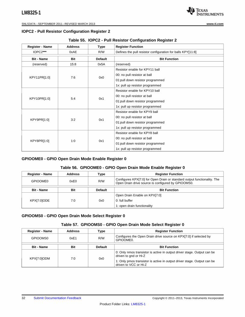
IOPC2 - Pull Resistor Configuration Register 2
Table 55. IOPC2 - Pull Resistor Configuration Register 2
Register - Name Address Type Register Function
IOPC2*** 0xAE R/W Defines the pull resistor configuration for balls KPY[11:8]
Bit - Name Bit Default Bit Function
(reserved) 15:8 0x5A (reserved)
Resistor enable for KPY11 ball
00: no pull resistor at ballKPY11PR[1:0] 7:6 0x0
01:pull down resistor programmed
1x: pull up resistor programmed
Resistor enable for KPY10 ball
00: no pull resistor at ballKPY10PR[1:0] 5:4 0x1
01:pull down resistor programmed
1x: pull up resistor programmed
Resistor enable for KPY9 ball
00: no pull resistor at ballKPY9PR[1:0] 3:2 0x1
01:pull down resistor programmed
1x: pull up resistor programmed
Resistor enable for KPY8 ball
00: no pull resistor at ballKPY8PR[1:0] 1:0 0x1
01:pull down resistor programmed
1x: pull up resistor programmed
GPIOOME0 - GPIO Open Drain Mode Enable Register 0
Table 56. GPIOOME0 - GPIO Open Drain Mode Enable Register 0
Register - Name Address Type Register Function
Configures KPX[7:0] for Open Drain or standard output functionality. TheGPIOOME0 0xE0 R/W Open Drain drive source is configured by GPIOOMS0.
Bit - Name Bit Default Bit Function
Open Drain Enable on KPX[7:0]
KPX[7:0]ODE 7:0 0x0 0: full buffer
1: open drain functionality
GPIOOMS0 - GPIO Open Drain Mode Select Register 0
Table 57. GPIOOMS0 - GPIO Open Drain Mode Select Register 0
Register - Name Address Type Register Function
Configures the Open Drain drive source on KPX[7:0] if selected byGPIOOMS0 0xE1 R/W GPIOOME0.
Bit - Name Bit Default Bit Function
0: Only nmos transistor is active in output driver stage. Output can bedriven to gnd or Hi-Z
KPX[7:0]ODM 7:0 0x01: Only pmos transistor is active in output driver stage. Output can bedriven to VCC or Hi-Z
32 Submit Documentation Feedback Copyright © 2011–2013, Texas Instruments Incorporated
Product Folder Links: LM8325-1

LM8325-1
www.ti.com SNLS347A –SEPTEMBER 2011–REVISED MARCH 2013
GPIOOME1 - GPIO Open Drain Mode Enable Register 1
Table 58. GPIOOME1 - GPIO Open Drain Mode Enable Register 1
Register - Name Address Type Register Function
Configures KPY[7:0] for Open Drain or standard output functionality. TheGPIOOME1 0xE2 R/W Open Drain drive source is configured by GPIOOMS1.
Bit - Name Bit Default Bit Function
Open Drain Enable on KPY[7:0]
KPY[7:0]ODE 7:0 0x0 0: full buffer
1: open drain functionality
GPIOOMS1 - GPIO Open Drain Mode Select Register 1
Table 59. GPIOOMS1 - GPIO Open Drain Mode Select Register 1
Register - Name Address Type Register Function
Configures the Open Drain drive source on KPY[7:0] if selected byGPIOOMS1 0xE3 R/W GPIOOME1.
Bit - Name Bit Default Bit Function
0: Only nmos transistor is active in output driver stage. Output can bedriven to gnd or Hi-Z
KPY[7:0]ODM 7:0 0x01: Only pmos transistor is active in output driver stage. Output can bedriven to VCC or Hi-Z
GPIOOME2 - GPIO Open Drain Mode Enable Register 2
Table 60. GPIOOME2 - GPIO Open Drain Mode Enable Register 2
Register - Name Address Type Register Function
Configures KPY[11:8] for Open Drain or standard output functionality. TheGPIOOME2 0xE4 R/W Open Drain drive source is configured by GPIOOMS2.
Bit - Name Bit Default Bit Function
(reserved) 7:4 0x0 (reserved)
Open Drain Enable on KPY[11:8]
0: full bufferKPY[11:8]ODE 3:0 0x81: open drain functionalityNote: KPY11/IRQN ball defaults to Open Drain Mode Enable after reset.
GPIOOMS2 - GPIO Open Drain Mode Select Register 2
Table 61. GPIOOMS2 - GPIO Open Drain Mode Select Register 2
Register - Name Address Type Register Function
Configures the Open Drain drive source on KPY[11:8] if selected byGPIOOMS2 0xE5 R/W GPIOOME2.
Bit - Name Bit Default Bit Function
(reserved 7:4 (reserved
0: Only nmos transistor is active in output driver stage. Output can bedriven to gnd or Hi-Z
KPY[11:8]ODM 3:0 0x01: Only pmos transistor is active in output driver stage. Output can bedriven to VCC or Hi-Z
Copyright © 2011–2013, Texas Instruments Incorporated Submit Documentation Feedback 33
Product Folder Links: LM8325-1

LM8325-1
SNLS347A –SEPTEMBER 2011–REVISED MARCH 2013 www.ti.com
GPIO DATA INPUT/OUTPUT
GPIOPDATA0 - GPIO Data Register 0
Table 62. GPIOPDATA0 - GPIO Data Register 0
Register - Name Address Type Register Function
This register is used for data input/output of KPX[7:0]. Every data I/O ismasked with the associated MASK register.
If one of the I/Os is defined as output (see Table 65) values written to thisGPIODATA0 0xC0 R/W register are masked with MASK and then applied to the associated pin.
If one of the I/Os is defined as input (see Table 65) values read from thisregister hold the masked input value of the associated pin.
Bit - Name Bit Default Bit Function
Mask Status for KPX7 when enabled as GPIO
MASK7 15 0x0 1: KPX7 enabled
0: KPX7 disabled
Mask Status for KPX6 when enabled as GPIO
MASK6 14 0x0 1: KPX6 enabled
0: KPX6 disabled
Mask Status for KPX5 when enabled as GPIO
MASK5 13 0x0 1: KPX5 enabled
0: KPX5 disabled
Mask Status for KPX4 when enabled as GPIO
MASK4 12 0x0 1: KPX4 enabled
0: KPX4 disabled
Mask Status for KPX3 when enabled as GPIO
MASK3 11 0x0 1: KPX3 enabled
0: KPX3 disabled
Mask Status for KPX2 when enabled as GPIO
MASK2 10 0x0 1: KPX2 enabled
0: KPX2 disabled
Mask Status for KPX1 when enabled as GPIO
MASK1 9 0x0 1: KPX1 enabled
0: KPX1 disabled
Mask Status for KPX0 when enabled as GPIO
MASK0 8 0x0 1: KPX0 enabled
0: KPX0 disabled
DATA7 7 0x0 Pin Status for KPX7 when enabled as GPIO
DATA6 6 0x0 Pin Status for KPX6 when enabled as GPIO
DATA5 5 0x0 Pin Status for KPX5 when enabled as GPIO
DATA4 4 0x0 Pin Status for KPX4 when enabled as GPIO
DATA3 3 0x0 Pin Status for KPX3 when enabled as GPIO
DATA2 2 0x0 Pin Status for KPX2 when enabled as GPIO
DATA1 1 0x0 Pin Status for KPX1 when enabled as GPIO
34 Submit Documentation Feedback Copyright © 2011–2013, Texas Instruments Incorporated
Product Folder Links: LM8325-1

LM8325-1
www.ti.com SNLS347A –SEPTEMBER 2011–REVISED MARCH 2013
Table 62. GPIOPDATA0 - GPIO Data Register 0 (continued)
Register - Name Address Type Register Function
DATA0 0 0x0 Pin Status for KPX0 when enabled as GPIO
GPIOPDATA1 - GPIO Data Register 1
Table 63. GPIOPDATA1 - GPIO Data Register 1
Register - Name Address Type Register Function
This register is used for data input/output of KPY[7:0]. Every data I/O ismasked with the associated MASK register.
If one of the I/Os is defined as output (see Table 66) values written to thisGPIODATA1 0xC2 R/W register are masked with MASK and then applied to the associated pin.
If one of the I/Os is defined as input (see Table 66) values read from thisregister hold the masked input value of the associated pin.
Bit - Name Bit Default Bit Function
Mask Status for KPY7 when enabled as GPIO
MASK15 15 0x0 1: KPY7 enabled
0: KPY7 disabled
Mask Status for KPY6 when enabled as GPIO
MASK14 14 0x0 1: KPY6 enabled
0: KPY6 disabled
Mask Status for KPY5 when enabled as GPIO
MASK13 13 0x0 1: KPY5 enabled
0: KPY5 disabled
Mask Status for KPY4 when enabled as GPIO
MASK12 12 0x0 1: KPY4 enabled
0: KPY4 disabled
Mask Status for KPY3 when enabled as GPIO
MASK11 11 0x0 1: KPY3 enabled
0: KPY3 disabled
Mask Status for KPY2 when enabled as GPIO
MASK10 10 0x0 1: KPY2 enabled
0: KPY2 disabled
Mask Status for KPY1 when enabled as GPIO
MASK9 9 0x0 1: KPY1 enabled
0: KPY1 disabled
Mask Status for KPY0 when enabled as GPIO
MASK8 8 0x0 1: KPY0 enabled
0: KPY0 disabled
DATA15 7 0x0 Pin Status for KPY7 when enabled as GPIO
DATA14 6 0x0 Pin Status for KPY6 when enabled as GPIO
DATA13 5 0x0 Pin Status for KPY5 when enabled as GPIO
DATA12 4 0x0 Pin Status for KPY4 when enabled as GPIO
DATA11 3 0x0 Pin Status for KPY3 when enabled as GPIO
DATA10 2 0x0 Pin Status for KPY2 when enabled as GPIO
DATA9 1 0x0 Pin Status for KPY1 when enabled as GPIO
DATA8 0 0x0 Pin Status for KPY0 when enabled as GPIO
Copyright © 2011–2013, Texas Instruments Incorporated Submit Documentation Feedback 35
Product Folder Links: LM8325-1
LM8325-1
SNLS347A –SEPTEMBER 2011–REVISED MARCH 2013 www.ti.com
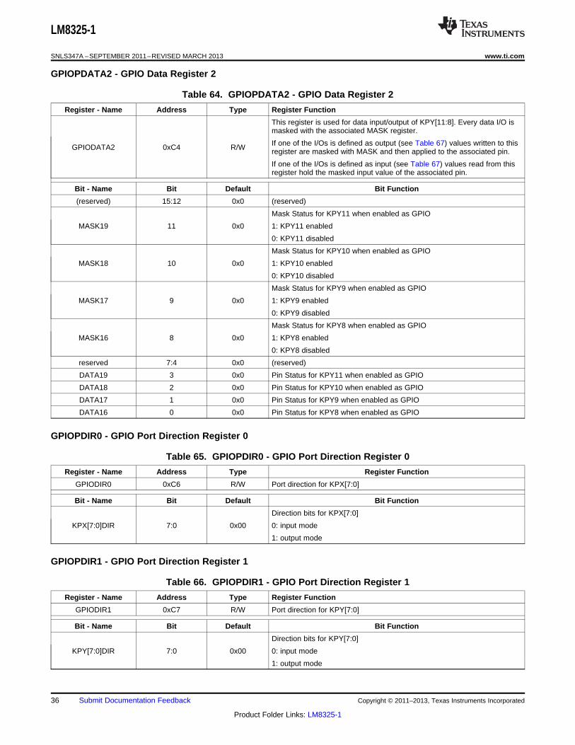
GPIOPDATA2 - GPIO Data Register 2
Table 64. GPIOPDATA2 - GPIO Data Register 2
Register - Name Address Type Register Function
This register is used for data input/output of KPY[11:8]. Every data I/O ismasked with the associated MASK register.
If one of the I/Os is defined as output (see Table 67) values written to thisGPIODATA2 0xC4 R/W register are masked with MASK and then applied to the associated pin.
If one of the I/Os is defined as input (see Table 67) values read from thisregister hold the masked input value of the associated pin.
Bit - Name Bit Default Bit Function
(reserved) 15:12 0x0 (reserved)
Mask Status for KPY11 when enabled as GPIO
MASK19 11 0x0 1: KPY11 enabled
0: KPY11 disabled
Mask Status for KPY10 when enabled as GPIO
MASK18 10 0x0 1: KPY10 enabled
0: KPY10 disabled
Mask Status for KPY9 when enabled as GPIO
MASK17 9 0x0 1: KPY9 enabled
0: KPY9 disabled
Mask Status for KPY8 when enabled as GPIO
MASK16 8 0x0 1: KPY8 enabled
0: KPY8 disabled
reserved 7:4 0x0 (reserved)
DATA19 3 0x0 Pin Status for KPY11 when enabled as GPIO
DATA18 2 0x0 Pin Status for KPY10 when enabled as GPIO
DATA17 1 0x0 Pin Status for KPY9 when enabled as GPIO
DATA16 0 0x0 Pin Status for KPY8 when enabled as GPIO
GPIOPDIR0 - GPIO Port Direction Register 0
Table 65. GPIOPDIR0 - GPIO Port Direction Register 0
Register - Name Address Type Register Function
GPIODIR0 0xC6 R/W Port direction for KPX[7:0]
Bit - Name Bit Default Bit Function
Direction bits for KPX[7:0]
KPX[7:0]DIR 7:0 0x00 0: input mode
1: output mode
GPIOPDIR1 - GPIO Port Direction Register 1
Table 66. GPIOPDIR1 - GPIO Port Direction Register 1
Register - Name Address Type Register Function
GPIODIR1 0xC7 R/W Port direction for KPY[7:0]
Bit - Name Bit Default Bit Function
Direction bits for KPY[7:0]
KPY[7:0]DIR 7:0 0x00 0: input mode
1: output mode
36 Submit Documentation Feedback Copyright © 2011–2013, Texas Instruments Incorporated
Product Folder Links: LM8325-1

LM8325-1
www.ti.com SNLS347A –SEPTEMBER 2011–REVISED MARCH 2013
GPIOPDIR2 - GPIO Port Direction Register 2
Table 67. GPIOPDIR2 - GPIO Port Direction Register 2
Register - Name Address Type Register Function
GPIODIR2 0xC8 R/W Port direction for KPY[11:8]
Bit - Name Bit Default Bit Function
(reserved) 7:4 (reserved)
Direction bits for KPY[11:8]
KPY[11:8]DIR 3:0 0x08 0: input mode
1: output mode
GPIO INTERRUPT CONTROL
GPIOIS0 - Interrupt Sense Configuration Register 0
Table 68. GPIOIS0 - Interrupt Sense Configuration Register 0
Register - Name Address Type Register Function
GPIOIS0 0xC9 R/W Interrupt type on KPX[7:0]
Bit - Name Bit Default Bit Function
Interrupt type bits for KPX[7:0]
KPX[7:0]IS 7:0 0x0 0: edge sensitive interrupt
1: level sensitive interrupt
GPIOIS1 - Interrupt Sense Configuration Register 1
Table 69. GPIOIS1 - Interrupt Sense Configuration Register 1
Register - Name Address Type Register Function
GPIOIS1 0xCA R/W Interrupt type on KPY[7:0]
Bit - Name Bit Default Bit Function
Interrupt type bits for KPY[7:0]
KPY[7:0]IS 7:0 0x0 0: edge sensitive interrupt
1: level sensitive interrupt
GPIOIS2 - Interrupt Sense Configuration Register 2
Table 70. GPIOIS2 - Interrupt Sense Configuration Register 2
Register - Name Address Type Register Function
GPIOIS2 0xCB R/W Interrupt type on KPY[11:8]
Bit - Name Bit Default Bit Function
(reserved) 7:4 (reserved)
Interrupt type bits for KPY[11:8]
KPY[11:8]IS 3:0 0x0 0: edge sensitive interrupt
1: level sensitive interrupt
Copyright © 2011–2013, Texas Instruments Incorporated Submit Documentation Feedback 37
Product Folder Links: LM8325-1

LM8325-1
SNLS347A –SEPTEMBER 2011–REVISED MARCH 2013 www.ti.com
GPIOIBE0 - GPIO Interrupt Edge Configuration Register 0
Table 71. GPIOIBE0 - GPIO Interrupt Edge Configuration Register 0
Register - Name Address Type Register Function
Defines whether an interrupt on KPX[7:0] is triggered on both edges or onGPIOIBE0 0xCC R/W a single edge. See Table 74 for the edge configuration.
Bit - Name Bit Default Bit Function
Interrupt both edges bits for KPX[7:0]
KPX[7:0]IBE 7:0 0x0 0: interrupt generated at the active edge
1: interrupt generated after both edges
GPIOIBE1 - GPIO Interrupt Edge Configuration Register 1
Table 72. GPIOIBE1 - GPIO Interrupt Edge Configuration Register 1
Register - Name Address Type Register Function
Defines whether an interrupt on KPY[7:0] is triggered on both edges or onGPIOIBE1 0xCD R/W a single edge. See Table 75 for the edge configuration.
Bit - Name Bit Default Bit Function
Interrupt both edges bits for KPY[7:0]
KPY[7:0]IBE 7:0 0x0 0: interrupt generated at the configured edge
1: interrupt generated after both edges
GPIOIBE2 - GPIO Interrupt Edge Configuration Register 2
Table 73. GPIOIBE2 - GPIO Interrupt Edge Configuration Register 2
Register - Name Address Type Register Function
Defines whether an interrupt on KPY[11:8] is triggered on both edges orGPIOIBE2 0xCE R/W on a single edge. See Table 76 for the edge configuration.
Bit - Name Bit Default Bit Function
(reserved 7:4 (reserved)
Interrupt both edges bits for KPY[11:8]
KPY[11:8]IBE 3:0 0x0 0: interrupt generated at the active edge
1: interrupt generated after both edges
GPIOIEV0 - GPIO Interrupt Edge Select Register 0
Table 74. GPIOIEV0 - GPIO Interrupt Edge Select Register 0
Register - Name Address Type Register Function
GPIOIEV0 0xCF R/W Select Interrupt edge for KPX[7:0].
Bit - Name Bit Default Bit Function
Interrupt edge select from KPX[7:0]
KPX[7:0]EV 7:0 0xFF 0: interrupt at low level or falling edge
1: interrupt at high level or rising edge
GPIOIEV1 - GPIO Interrupt Edge Select Register 1
Table 75. GPIOIEV1 - GPIO Interrupt Edge Select Register 1
Register - Name Address Type Register Function
GPIOIEV1 0xD0 R/W Select Interrupt edge for KPY[7:0].
Bit - Name Bit Default Bit Function
38 Submit Documentation Feedback Copyright © 2011–2013, Texas Instruments Incorporated
Product Folder Links: LM8325-1
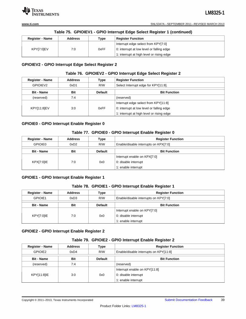
LM8325-1
www.ti.com SNLS347A –SEPTEMBER 2011–REVISED MARCH 2013
Table 75. GPIOIEV1 - GPIO Interrupt Edge Select Register 1 (continued)
Register - Name Address Type Register Function
Interrupt edge select from KPY[7:0]
KPY[7:0]EV 7:0 0xFF 0: interrupt at low level or falling edge
1: interrupt at high level or rising edge
GPIOIEV2 - GPIO Interrupt Edge Select Register 2
Table 76. GPIOIEV2 - GPIO Interrupt Edge Select Register 2
Register - Name Address Type Register Function
GPIOIEV2 0xD1 R/W Select Interrupt edge for KPY[11:8].
Bit - Name Bit Default Bit Function
(reserved) 7:4 (reserved)
Interrupt edge select from KPY[11:8]
KPY[11:8]EV 3:0 0xFF 0: interrupt at low level or falling edge
1: interrupt at high level or rising edge
GPIOIE0 - GPIO Interrupt Enable Register 0
Table 77. GPIOIE0 - GPIO Interrupt Enable Register 0
Register - Name Address Type Register Function
GPIOIE0 0xD2 R/W Enable/disable interrupts on KPX[7:0]
Bit - Name Bit Default Bit Function
Interrupt enable on KPX[7:0]
KPX[7:0]IE 7:0 0x0 0: disable interrupt
1: enable interrupt
GPIOIE1 - GPIO Interrupt Enable Register 1
Table 78. GPIOIE1 - GPIO Interrupt Enable Register 1
Register - Name Address Type Register Function
GPIOIE1 0xD3 R/W Enable/disable interrupts on KPY[7:0]
Bit - Name Bit Default Bit Function
Interrupt enable on KPY[7:0]
KPY[7:0]IE 7:0 0x0 0: disable interrupt
1: enable interrupt
GPIOIE2 - GPIO Interrupt Enable Register 2
Table 79. GPIOIE2 - GPIO Interrupt Enable Register 2
Register - Name Address Type Register Function
GPIOIE2 0xD4 R/W Enable/disable interrupts on KPY[11:8]
Bit - Name Bit Default Bit Function
(reserved) 7:4 (reserved)
Interrupt enable on KPY[11:8]
KPY[11:8]IE 3:0 0x0 0: disable interrupt
1: enable interrupt
Copyright © 2011–2013, Texas Instruments Incorporated Submit Documentation Feedback 39
Product Folder Links: LM8325-1

LM8325-1
SNLS347A –SEPTEMBER 2011–REVISED MARCH 2013 www.ti.com
GPIOIC0 - GPIO Clear Interrupt Register 0
Table 80. GPIOIC0 - GPIO Clear Interrupt Register 0
Register - Name Address Type Register Function
GPIOIC0 0xDC W Clears the interrupt on KPX[7:0]
Bit - Name Bit Default Bit Function
Clear Interrupt on KPX[7:0]
KPX[7:0]IC 7:0 0: no effect
1: Clear corresponding interrupt
GPIOIC1 - GPIO Clear Interrupt Register 1
Table 81. GPIOIC1 - GPIO Clear Interrupt Register 1
Register - Name Address Type Register Function
GPIOIC1 0xDD W Clears the interrupt on KPY[7:0]
Bit - Name Bit Default Bit Function
Clear Interrupt on KPY[7:0]
KPY[7:0]IC 7:0 0: no effect
1: Clear corresponding interrupt
GPIOIC2 - GPIO Clear Interrupt Register 2
Table 82. GPIOIC2 - GPIO Clear Interrupt Register 2
Register - Name Address Type Register Function
GPIOIC2 0xDE W Clears the interrupt on KPY[11:8]
Bit - Name Bit Default Bit Function
(reserved) 7:4 (reserved)
Clear Interrupt on KPY[11:8]
KPY[11:8]IC 3:0 0: no effect
1: Clear corresponding interrupt
GPIO INTERRUPT STATUS
GPIORIS0 - Raw Interrupt Status Register 0
Table 83. GPIORIS0 - Raw Interrupt Status Register 0
Register - Name Address Type Register Function
GPIORIS0 0xD6 R Raw interrupt status on KPX[7:0]
Bit - Name Bit Default Bit Function
Raw Interrupt status data on KPX[7:0]
KPX[7:0]RIS 7:0 0x0 0: no interrupt condition at GPIO
1: interrupt condition at GPIO
GPIORIS1 - Raw Interrupt Status Register 1
Table 84. GPIORIS1 - Raw Interrupt Status Register 1
Register - Name Address Type Register Function
GPIORIS1 0xD7 R Raw interrupt status on KPY[7:0]
Bit - Name Bit Default Bit Function
40 Submit Documentation Feedback Copyright © 2011–2013, Texas Instruments Incorporated
Product Folder Links: LM8325-1

LM8325-1
www.ti.com SNLS347A –SEPTEMBER 2011–REVISED MARCH 2013
Table 84. GPIORIS1 - Raw Interrupt Status Register 1 (continued)
Register - Name Address Type Register Function
Raw Interrupt status data on KPY[7:0]
KPY[7:0]RIS 7:0 0x0 0: no interrupt condition at GPIO
1: interrupt condition at GPIO
GPIORIS2 - Raw Interrupt Status Register 2
Table 85. GPIORIS2 - Raw Interrupt Status Register 2
Register - Name Address Type Register Function
GPIORIS2 0xD8 R Raw interrupt status on KPY[11:8]
Bit - Name Bit Default Bit Function
(reserved) 7:4 (reserved)
Raw Interrupt status data on KPY[11:8]
KPY[11:8]RIS 3:0 0x0 0: no interrupt condition at GPIO
1: interrupt condition at GPIO
GPIOMIS0 - Masked Interrupt Status Register 0
Table 86. GPIOMIS0 - Masked Interrupt Status Register 0
Register - Name Address Type Register Function
GPIOMIS0 0xD9 R Masked interrupt status on KPX[7:0]
Bit - Name Bit Default Bit Function
Masked Interrupt status data on KPX[7:0]
KPX[7:0]MIS 7:0 0x0 0: no interrupt contribution from GPIO
1: interrupt GPIO is active
GPIOMIS1 - Masked Interrupt Status Register 1
Table 87. GPIOMIS1 - Masked Interrupt Status Register 1
Register - Name Address Type Register Function
GPIOMIS1 0xDA R Masked interrupt status on KPY[7:0]
Bit - Name Bit Default Bit Function
Masked Interrupt status data on KPY[7:0]
KPY[7:0]MIS 7:0 0x0 0: no interrupt contribution from GPIO
1: interrupt GPIO is active
GPIOMIS2 - Masked Interrupt Status Register 2
Table 88. GPIOMIS2 - Masked Interrupt Status Register 2
Register - Name Address Type Register Function
GPIOMIS2 0xDB R Masked interrupt status on KPY[11:8]
Bit - Name Bit Default Bit Function
(reserved) 7:4 (reserved)
Masked Interrupt status data on KPY[11:8]
KPY[11:8]MIS 3:0 0x0 0: no interrupt contribution from GPIO
1: interrupt GPIO is active
Copyright © 2011–2013, Texas Instruments Incorporated Submit Documentation Feedback 41
Product Folder Links: LM8325-1
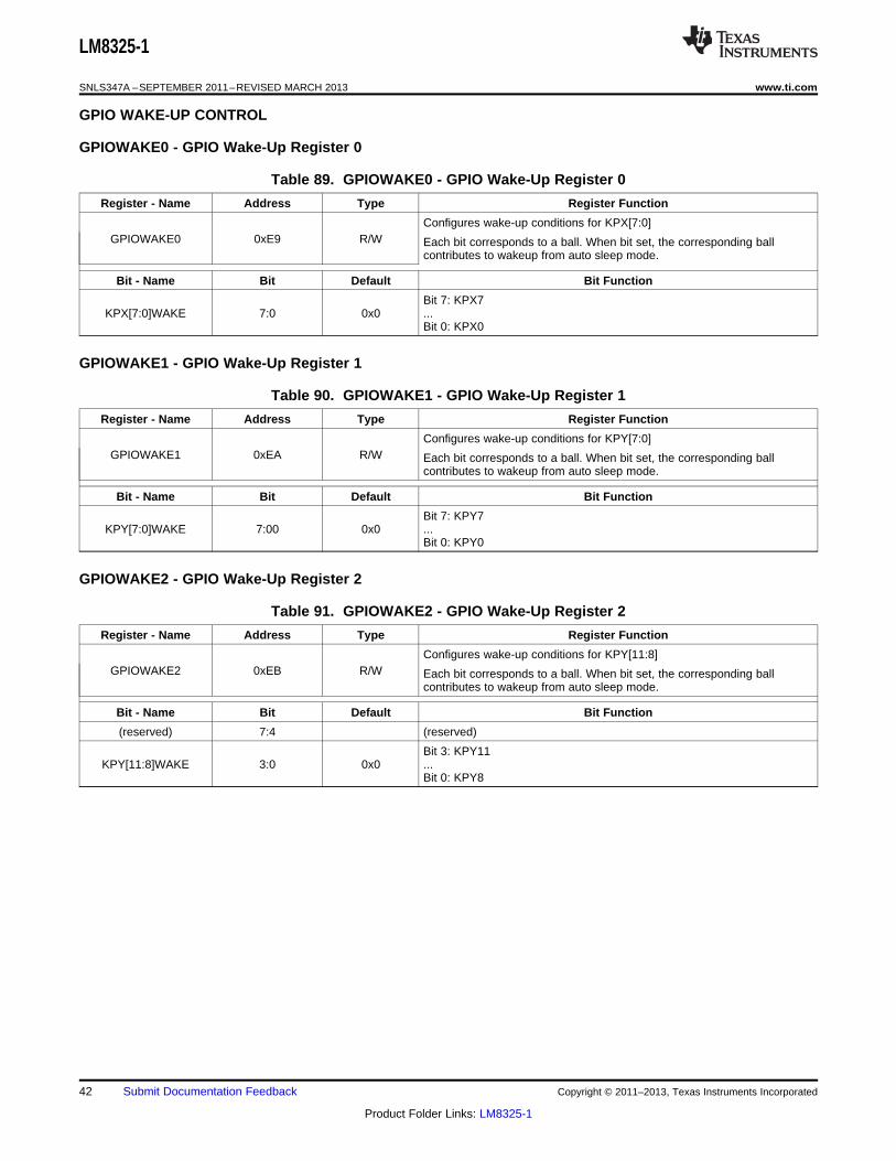
LM8325-1
SNLS347A –SEPTEMBER 2011–REVISED MARCH 2013 www.ti.com
GPIO WAKE-UP CONTROL
GPIOWAKE0 - GPIO Wake-Up Register 0
Table 89. GPIOWAKE0 - GPIO Wake-Up Register 0
Register - Name Address Type Register Function
Configures wake-up conditions for KPX[7:0]GPIOWAKE0 0xE9 R/W Each bit corresponds to a ball. When bit set, the corresponding ball
contributes to wakeup from auto sleep mode.
Bit - Name Bit Default Bit Function
Bit 7: KPX7KPX[7:0]WAKE 7:0 0x0 ...
Bit 0: KPX0
GPIOWAKE1 - GPIO Wake-Up Register 1
Table 90. GPIOWAKE1 - GPIO Wake-Up Register 1
Register - Name Address Type Register Function
Configures wake-up conditions for KPY[7:0]GPIOWAKE1 0xEA R/W Each bit corresponds to a ball. When bit set, the corresponding ball
contributes to wakeup from auto sleep mode.
Bit - Name Bit Default Bit Function
Bit 7: KPY7KPY[7:0]WAKE 7:00 0x0 ...
Bit 0: KPY0
GPIOWAKE2 - GPIO Wake-Up Register 2
Table 91. GPIOWAKE2 - GPIO Wake-Up Register 2
Register - Name Address Type Register Function
Configures wake-up conditions for KPY[11:8]GPIOWAKE2 0xEB R/W Each bit corresponds to a ball. When bit set, the corresponding ball
contributes to wakeup from auto sleep mode.
Bit - Name Bit Default Bit Function
(reserved) 7:4 (reserved)
Bit 3: KPY11KPY[11:8]WAKE 3:0 0x0 ...
Bit 0: KPY8
42 Submit Documentation Feedback Copyright © 2011–2013, Texas Instruments Incorporated
Product Folder Links: LM8325-1

LM8325-1
www.ti.com SNLS347A –SEPTEMBER 2011–REVISED MARCH 2013
These devices have limited built-in ESD protection. The leads should be shorted together or the device placed in conductive foamduring storage or handling to prevent electrostatic damage to the MOS gates.
ABSOLUTE MAXIMUM RATINGS (1) (2)
Supply Voltage (VCC) −0.3V to 2.2V
Voltage at Generic IOs −0.2V to VCC +0.2V
Voltage at Backdrive/Overvoltage IOs −0.3V to +.4.25V
Maximum Input Current Without Latchup ±100 mA
ESD Protection Level (Human Body Model) 2kV
(Machine Model) 200V
(Charge Device Model) 750V
Total Current into VCC Pin (Source) 100 mA
Total Current out of GND Pin (Sink) 100 mA
Storage Temperature Range −65°C to +140°C
(1) Absolute Maximum Ratings indicate limits beyond which damage to the device may occur. Operating Ratings indicate conditions forwhich the device is intended to be functional, but specific performance is not ensured. For ensured specifications and test conditions,see the Electrical Characteristics tables.
(2) If Military/Aerospace specified devices are required, please contact the TI Sales Office/ Distributors for availability and specifications.
DC ELECTRICAL CHARACTERISTICSDatasheet min/max specification limits are specified by design, test, or statistical analysis.(Temperature: −40°C ≤ TA ≤ +85°C, unless otherwise specified)
Parameter Conditions Min Typ Max Units
Operating Voltage (VCC) Core Supply Voltage 1.62 1.98 V
Maximum Input voltage for Backdrive/Overvoltage IOs 3.60 V
Internal Clock = ON, all internal functionalblocks running
Supply Current (IDD) (1) No loads on pins, 1.9 3.0 mA
VCC = 1.8V, TC = 0.5 µsTA = 25°C
Sleep Mode HALT Current (IHALT) (2) VCC = 1.8V, TA = 25°C;Internal Clock = OFF, no internal functional <9 40 µAblocks running
IDLE Current Internal Clock = ON, no internal functional 1 mAblocks running
(1) Supply and IDLE current is measured with inputs connected to VCC and outputs driven low but not connected to a load.(2) In sleep mode, the internal clock is switched off. Supply current in sleep mode is measured with inputs connected to VCC and outputs
driven low but not connected to a load.
AC ELECTRICAL CHARACTERISTICS(Temperature: −40°C ≤ TA ≤ +85°C)Data sheet specification limits are specified by design, test, or statistical analysis.
Parameter Conditions Min Typ Max Units
System Clock Frequency Internal RC 21 MHz
System Clock Period (mclk) 1.62V ≤ VCC ≤ 1.98V 48 ns
Internal RC Oscillator (tC) 1.62V ≤ VCC ≤ 1.98V 0.5 μs
Internal RC Oscillator Frequency Variation ±7 %
Copyright © 2011–2013, Texas Instruments Incorporated Submit Documentation Feedback 43
Product Folder Links: LM8325-1

LM8325-1
SNLS347A –SEPTEMBER 2011–REVISED MARCH 2013 www.ti.com
AC ELECTRICAL CHARACTERISTICS (continued)(Temperature: −40°C ≤ TA ≤ +85°C)Data sheet specification limits are specified by design, test, or statistical analysis.
Parameter Conditions Min Typ Max Units
ACCESS.bus Input Signals
Bus Free Time Between Stop and Start 16Condition (tBUFi)
(1)
SCL Setup Time (tCSTOsi)(1) Before Stop Condition 8
SCL Hold Time (tCSTRhi)(1) After Start Condition 8
SCL Setup Time (tCSTRsi)(1) Before Start Condition 8
mclkData High Setup Time (tDHCsi)(1) (2) Before SCL Rising Edge (RE) 2
Data Low Setup Time (tDLCsi)(1) (2) Before SCL RE 2
SCL Low Time (tSCLlowi)(1) After SCL Falling Edge (FE) 12
SCL High Time (tSCLhighi)(1) (2) After SCL FE 12
SDA Hold Time (tSDAhi)(1) After SCL FE 0
SDA Setup Time (tSDAsi)(1) (2) Before SCL RE 2
ACCESS.bus Output Signals
SDA Hold Time (tSDAho) (1) After SCL Falling Edge 2 mclk
(1) Specified by design, not tested.(2) The ACCESS.bus interface implements and meets the timings necessary for interface to the I2C and SMBus protocols at logic levels.
The bus drivers have open-drain outputs for bidirectional operation. Due to Internal RC Oscillator Frequency Variation, this specificationmay not meet the AC timing and current/voltage drive requirements of the full-bus specifications.
GENERAL GPIO CHARACTERISTICSCharacteristics for all pins except CLKIN, IRQN/KPY11/PWM2, SDA, and SCL in GPIO mode.
Parameter Conditions Min Typ Max Units
VIH (Min. Input High Voltage) 0.7xVCC V
VIL (Max. Input Low Voltage) 0.3xVCC V
VCC = 1.62ISource −16 mAVOH = 0.7xVCC
VCC = 1.62ISink 16 mAVOL = 0.3xVCC
Allowable Sink current per pin (1) 16 mA
IPU (Weak Pull-UP Current) (2) VOUT = 0V -30 -160
IPD (Weak Pull-Down Current) (2) VOUT = VCC 30 160µA
GPIO output disabledIOZ (Input Leakage Current) ±2
Vpin = 0 to VCC
tRise/Fall (Max. Rise and Fall times) (3) CLOAD = 50 pF 15 ns
(1) The sum of all I/O sink/source current must not exceed the maximum total current into VCC and out of GND as specified in the absolutemaximum ratings.
(2) This is the internal weak pull-up (pull-down) current when driver output is disabled. If enabled, during receiving mode, this is the currentrequired to switch the input from one state to another.
(3) Specified by design, not tested.
44 Submit Documentation Feedback Copyright © 2011–2013, Texas Instruments Incorporated
Product Folder Links: LM8325-1

LM8325-1
www.ti.com SNLS347A –SEPTEMBER 2011–REVISED MARCH 2013
BACKDRIVE/OVERVOLTAGE I/O DC CHARACTERISTICSCharacteristics for pins CLKIN, IRQN/KPY11/PWM2, SDA and SCL
Parameter Conditions Min Typ Max Units
VIH (Min. Input High Voltage) 0.7xVCCV
VIL (Max. Input Low Voltage) 0.3xVCC
VCC = 1.62VISource -6 mAVOH = 1.5V
VCC = 1.62VISink1 (as GPIO) 12 mAVOL = 0.4V
VCC = 1.62VISink2 (as ACCESS.bus) 3 mAVOL = 0.4V
VCC = 1.62VISink3 (as ACCESS.bus) 4 mAVOL = 0.6V
Allowable Sink current per pin (1) 12 mA
IPU (Weak Pull-UP Current) (2) VOUT = 0V -7 -40
IPD (Weak Pull-Down Current) (2) VOUT = VCC 7 40
GPIO output disabledµA
VCC = 1.62V to 1.98VIOZ1 (Input Leakage Current) (3)
Vpin = 0 to VCC ±2
Vpin = VCC to 3.6V ±10
0 ≤ VCC ≤ 0.5VIOZ2 (Input Backdrive Leakage Current) ±10 µAVpin = 0 to 3.6V
(1) The sum of all I/O sink/source current must not exceed the maximum total current into VCC and out of GND as specified in the absolutemaximum ratings.
(2) This is the internal weak pull-up (pull-down) current when driver output is disabled. If enabled, during receiving mode, this is the currentrequired to switch the input from one state to another.
(3) IOZ1 for CLKIN is max 60 µA if VPIN > VCC because the weak pull-down is enabled.
BACKDRIVE/OVERVOLTAGE I/O AC CHARACTERISTICSCharacteristics for pins CLKIN, IRQN/KPY11/PWM2, SDA and SCL
Parameter Conditions Min Typ Max Units
tRise/Fall CLOAD=50 pF @ 1MHz 70(Max. Rise and Fall time) (1)
nstFall CLOAD=10 pF to 100 pF(Max. Fall time) as ACCESS.bus (SDA, SCL 10 120VIHmin to VILmaxonly) (1)
(1) Specified by design, not tested.
Copyright © 2011–2013, Texas Instruments Incorporated Submit Documentation Feedback 45
Product Folder Links: LM8325-1

LM8325-1
SNLS347A –SEPTEMBER 2011–REVISED MARCH 2013 www.ti.com
REGISTER
REGISTER MAPPING
Keyboard Registers
shows the register map for keyboard functionality. In addition to Global Call Reset (see Global Call Reset) orSoftware Reset using SWRESET (see Table 42), these registers are reset to 0x00 values by a module resetusing RSTCTRL.KBDRST and should be rewritten for desired settings (see Table 43).
Register Map for Keyboard FunctionalityRegister File Next RFRegister Name Description Register Type ACCESS Size Default valueAddress Address
Keypad SettleKBDSETTLE 0x01 R/W byte 0x80 0x02Time
Keypad DebounceKBDBOUNCE 0x02 R/W byte 0x80 0x03Time
Keypad SizeKBDSIZE 0x03 R/W byte 0x22 0x04Configuration
Keypad DedicatedKBDDEDCFG0 0x04 R/W byte 0xFF 0x05Key 0
Keypad DedicatedKBDDEDCFG1 0x05 R/W byte 0xFF 0x06Key 1
Keypad RawKBDRIS 0x06 R byte 0x00 0x07Interrupt Status
Keypad MaskedKBDMIS 0x07 R byte 0x00 0x08Interrupt Status
Keypad InterruptKBDIC 0x08 W byte 0x09Clear
Keypad InterruptKBDMSK 0x09 R/W byte 0xF3 0x0AMask
KBDCODE0 Keypad Code 0 0x0B R byte 0x7F 0x0C
KBDCODE1 Keypad Code 1 0x0C R byte 0x7F 0x0D
KBDCODE2 Keypad Code 2 0x0D R byte 0x7F 0x0E
KBDCODE3 Keypad Code 3 0x0E R byte 0x7F 0x0F
EVTCODE Key Event Code 0x10 R byte 0x7F 0x10
PWM Timer Registers
shows the register map for PWM Timer functionality. In addition to Global Call Reset (see Global Call Reset) orSoftware Reset using SWRESET (see Table 42), these registers are reset to default values by a module resetusing RSTCTRL.TIMRST (see Table 43).
Register Map for PWM Timer FunctionalityRegister File Next RFRegister Name Description Register Type ACCESS Size Default valueAddress Address
PWM TimerTIMCFG0 0x60 R/W byte 0x00 0x61Configuration 0
PWMPWMCFG0 0x61 R/W byte 0x00 0x62Configuration 0
PWM TimerTIMSCAL0 0x62 R/W byte 0x00 0x63Prescaler 0
PWM TimerTIMCFG1 0x68 R/W byte 0x00 0x69Configuration 1
PWMPWMCFG1 0x69 R/W byte 0x00 0x6AConfiguration 1
PWM TimerTIMSCAL1 0x6A R/W byte 0x00 0x6BPrescaler 1
46 Submit Documentation Feedback Copyright © 2011–2013, Texas Instruments Incorporated
Product Folder Links: LM8325-1

LM8325-1
www.ti.com SNLS347A –SEPTEMBER 2011–REVISED MARCH 2013
Register Map for PWM Timer Functionality (continued)
Register File Next RFRegister Name Description Register Type ACCESS Size Default valueAddress Address
PWM TimerTIMCFG2 0x70 R/W byte 0x00 0x71Configuration 2
PWMPWMCFG2 0x71 R/W byte 0x00 0x72Configuration 2
PWM TimerTIMSCAL2 0x72 R/W byte 0x00 0x73Prescaler 2
PWM Timer SWTIMSWRES 0x78 W byte 0x79Reset
PWM TimerTIMRIS 0x7A R byte 0x00 0x7BInterrupt Status
PWM TimerTIMMIS 0x7B R byte 0x00 0x7CMasked Int. Status
Timer InterruptTIMIC 0x7C W byte 0x7DClear
PWM CommandPWMWP 0x7D R/W byte 0x00 0x7EWrite Pointer
PWM CommandPWMCFG 0x7E W word 0x7FScript
System Registers
shows the register map for general system registers. These registers are not affected by any of the moduleresets addressed by RSTCTRL (see Table 43). These registers can only be reset to default values by a GlobalCall Reset (see Global Call Reset) or by a complete Software Reset using SWRESET (see Table 42).
Register Map for System Control FunctionalityRegister Name Description Register File Register Type ACCESS Size Default value Next RF
Address Address
I2C-compatibleI2CSA ACCESS.bus 0x80 W byte 0x88 0x81
Slave Address
MFGCODE Manufacturer Code 0x80 R byte 0x00 0x81
SWREV SW Revision 0x81 R byte 0x83 0x82
SWRESET SW Reset 0x81 W byte 0x82
RSTCTRL System Reset 0x82 R/W byte 0x00 0x83
Clear NoRSTINTCLR Init/Power On 0x84 W byte 0x85
Interrupt
CLKMODE Clock Mode 0x88 R/W byte 0x01 0x89
ClockCLKCFG 0x89 R/W byte 0x40 0x8AConfiguration
CLKEN Clock Enable 0x8A R/W byte 0x00 0x8B
AUTOSLP Auto Sleep Enable 0x8B R/W byte 0x00 0x8C
AUTOSLPTI Auto Sleep Time 0x8C R/W word 0x00FF 0x8D
Global Interrupt Registers
shows the register map for global interrupt functionality. In addition to Global Call Reset (see Global Call Reset)or Software Reset using SWRESET (see Table 42), these registers are reset to default values by a module resetusing RSTCTRL.IRQRST (see Table 43).
Copyright © 2011–2013, Texas Instruments Incorporated Submit Documentation Feedback 47
Product Folder Links: LM8325-1

LM8325-1
SNLS347A –SEPTEMBER 2011–REVISED MARCH 2013 www.ti.com
Register Map for Global Interrupt FunctionalityRegister Name Description Register File Register Type ACCESS Size Default value Next RF
Address Address
Global InterruptIRQST 0x91 R byte 0x80 0x92Status
GPIO Registers
shows the register map for GPIO functionality. In addition to Global Call Reset (see Global Call Reset) orSoftware Reset using SWRESET (see Table 42), these registers are reset to 0x00 values by a module resetusing RSTCTRL.GPIRST and should be rewritten for desired settings (see Table 43).
Register Map for GPIO FunctionalityRegister Name Description Register File Register Type ACCESS Size Default value Next RF
Address Address
I/O Pin MappingIOCFG 0xA7 W byte 0xA8Configuration
Pull ResistorIOPC0 0xAA R/W word 0xAAAA 0xABConfiguration 0
Pull ResistorIOPC1 0xAC R/W word 0x5555 0xADConfiguration 1
Pull ResistorIOPC2 0xAE R/W word 0x5A15 0xAFConfiguration 2
GPIODATA0 GPIO I/O Data 0 0xC0 R/W byte 0x00 0xC1
GPIOMASK0 GPIO I/O Mask 0 0xC1 W byte 0xC2
GPIODATA1 GPIO I/O Data 1 0xC2 R/W byte 0x00 0xC3
GPIOMASK1 GPIO I/O Mask 1 0xC3 W byte 0xC4
GPIODATA2 GPIO I/O Data 2 0xC4 R/W byte 0x00 0xC5
GPIOMASK2 GPIO I/O Mask 2 0xC5 W byte 0xC6
GPIO I/OGPIODIR0 0xC6 R/W byte 0x00 0xC7Direction 0
GPIO I/OGPIODIR1 0xC7 R/W byte 0x00 0xC8Direction 1
GPIO I/OGPIODIR2 0xC8 R/W byte 0x08 0xC9Direction 2
GPIO Int SenseGPIOIS0 0xC9 R/W byte 0x00 0xCAConfig 0
GPIO Int SenseGPIOIS1 0xCA R/W byte 0x00 0xCBConfig 1
GPIO Int SenseGPIOIS2 0xCB R/W byte 0x00 0xCCConfig 2
GPIO Int BothGPIOIBE0 0xCC R/W byte 0x00 0xCDEdges Config 0
GPIO Int BothGPIOIBE1 0xCD R/W byte 0x00 0xCEEdges Config 1
GPIO Int BothGPIOIBE2 0xCE R/W byte 0x00 0xCFEdges Config 2
GPIO Int EdgeGPIOIEV0 0xCF R/W byte 0xFF 0xD0Select 0
GPIO Int EdgeGPIOIEV1 0xD0 R/W byte 0xFF 0xD1Select 1
GPIO Int EdgeGPIOIEV2 0xD1 R/W byte 0xFF 0xD2Select 2
GPIO InterruptGPIOIE0 0xD2 R/W byte 0x00 0xD3Enable 0
GPIO InterruptGPIOIE1 0xD3 R/W byte 0x00 0xD4Enable 1
48 Submit Documentation Feedback Copyright © 2011–2013, Texas Instruments Incorporated
Product Folder Links: LM8325-1

LM8325-1
www.ti.com SNLS347A –SEPTEMBER 2011–REVISED MARCH 2013
Register Map for GPIO Functionality (continued)
Register Name Description Register File Register Type ACCESS Size Default value Next RFAddress Address
GPIO InterruptGPIOIE2 0xD4 R/W byte 0x00 0xD5Enable 2
GPIO Raw IntGPIORIS0 0xD6 R byte 0x00 0xD7Status 0
GPIO Raw IntGPIORIS1 0xD7 R byte 0x00 0xD8Status 1
GPIO Raw IntGPIORIS2 0xD8 R byte 0x00 0xD9Status 2
GPIO Masked IntGPIOMIS0 0xD9 R byte 0x00 0xDAStatus 0
GPIO Masked IntGPIOMIS1 0xDA R byte 0x00 0xDBStatus 1
GPIO Masked IntGPIOMIS2 0xDB R byte 0x00 0xDCStatus 2
GPIO InterruptGPIOIC0 0xDC W byte 0xDDClear 0
GPIO InterruptGPIOIC1 0xDD W byte 0xDEClear 1
GPIO InterruptGPIOIC2 0xDE W byte 0xDFClear 2
GPIO Open DrainGPIOOME0 0xE0 R/W byte 0x00 0xE1Mode Enable 0
GPIO Open DrainGPIOOMS0 0xE1 R/W byte 0x00 0xE2Mode Select 0
GPIO Open DrainGPIOOME1 0xE2 R/W byte 0x00 0xE3Mode Enable 1
GPIO Open DrainGPIOOMS1 0xE3 R/W byte 0x00 0xE4Mode Select 1
GPIO Open DrainGPIOOME2 0xE4 R/W byte 0x08 0xE5Mode Enable 2
GPIO Open DrainGPIOOMS2 0xE5 R/W byte 0x00 0xE6Mode Select 2
GPIO WakeupGPIOWAKE0 0xE9 R/W byte 0x00 0xEAEnable 0
GPIO WakeupGPIOWAKE1 0xEA R/W byte 0x00 0xEBEnable 1
GPIO WakeupGPIOWAKE2 0xEB R/W byte 0x00 0xECEnable 2
REGISTER LAYOUT - Control Bits in LM8325-1 RegistersRegister Addr. BIT 7 BIT 6 BIT 5 BIT 4 BIT 3 BIT 2 BIT 1 BIT 0
KBDSETTLE 0x01 Wait[7:0]
KBDBOUNCE 0x02 Wait[7:0]
ROW- ROW- ROW- ROW- COL- COL- COL- COL-KBDSIZE 0x03 SIZE3 SIZE2 SIZE1 SIZE0 SIZE3 SIZE2 SIZE1 SIZE0
KBDDEDCFG 0x04 COL9 COL8 COL7 COL6 COL5 COL4 COL3 COL20
KBDDEDCFG 0x05 ROW7 ROW6 ROW5 ROW4 ROW3 ROW2 COL11 COL101
KBDRIS 0x06 RELINT REVTINT RKLINT RSINT
KBDMIS 0x07 MELINT MEVTINT MKLINT MSINT
KBDIC 0x08 SFOFF EVTIC KBDIC
KBDMSK 0x09 MSKELINT MSKEINT MSKLINT MSKSINT
KBDCODE0 0x0B MULTIKEY KEYROW2 KEYROW1 KEYROW0 KEYCOL3 KEYCOL2 KEYCOL1 KEYCOL0
Copyright © 2011–2013, Texas Instruments Incorporated Submit Documentation Feedback 49
Product Folder Links: LM8325-1

LM8325-1
SNLS347A –SEPTEMBER 2011–REVISED MARCH 2013 www.ti.com
REGISTER LAYOUT - Control Bits in LM8325-1 Registers (continued)
Register Addr. BIT 7 BIT 6 BIT 5 BIT 4 BIT 3 BIT 2 BIT 1 BIT 0
KBDCODE1 0x0C MULTIKEY KEYROW2 KEYROW1 KEYROW0 KEYCOL3 KEYCOL2 KEYCOL1 KEYCOL0
KBDCODE2 0x0D MULTIKEY KEYROW2 KEYROW1 KEYROW0 KEYCOL3 KEYCOL2 KEYCOL1 KEYCOL0
KBDCODE3 0x0E MULTIKEY KEYROW2 KEYROW1 KEYROW0 KEYCOL3 KEYCOL2 KEYCOL1 KEYCOL0
EVTCODE 0x10 RELEASE KEYROW2 KEYROW1 KEYROW0 KEYCOL3 KEYCOL2 KEYCOL1 KEYCOL0
CICIRQ0-TIMCFG0 0x60 STARTMASK
CDIRQ0-PWMCFG0 0x61 PGE PWMEN PWMPOLMASK
TIMSCAL0 0x62 SCAL[7:0]
CYIRQ1TIMCFG1 0x68 STARTMASK
CDIRQ1-PWMCFG1 0x69 PGE PWMEN PWMPOLMASK
TIMSCAL1 0x6A SCAL7 SCAL6 SCAL5 SCAL4 SCAL3 SCAL2 SCAL1 SCAL0
TIMCFG2 0x70 IRQMASK START
CDIRQ2-PWMCFG2 0x71 PGE PWMEN PWMPOLMASK
TIMSCAL2 0x72 SCAL7 SCAL6 SCAL5 SCAL4 SCAL3 SCAL2 SCAL1 SCAL0
TIMSWRES 0x78 SWRES2 SWRES1 SWRES0
TIMRIS 0x7A CDIRQ2 CDIRQ1 CDIRQ0 CICIRQ2 CICIRQ1 CICIRQ0
TIMMIS 0x7B CDIRQ2 CDIRQ1 CDIRQ0 CICIRQ2 CICIRQ1 CICIRQ0
TIMIC 0x7C CDIRQ2 CDIRQ1 CDIRQ0 CICIRQ2 CICIRQ1 CICIRQ0
PWMWP 0x7D 0 PWMWP[6:0]
PWMCFG 0x7E CMD[7:0](Low)
PWMCFG 0x7F CMD[15:8](High)
I2CSA 0x80 SLAVEADDR[7:1] 0
MFGCODE 0x80 MFGBIT[7:0]
SWREV 0x81 SWBIT[7:0]
SWRESET 0x81 SWBIT[7:0]
RSTCTRL 0x82 IRQRST TIMRST KBDRST GPIRST
RSTINTCLR 0x84 IRQCLR
CLKMODE 0x88 MOD-CTL[1:0]
CLKCFG 0x89 CLKSRCSEL[1:0]
CLKEN 0x8A CLKOUTEN[1:0] TIMEN KBDEN
AUTOSLP 0x8B ENABLE
AUTOSLPTI 0x8C UP-TIME [7:0](Low)
AUTOSLPTI 0x8D UP-TIME [10:8](High)
IRQST 0x91 PORIRQ KBD1RQ TIM2IRQ TIM1IRQ TIM01RQ GPIIRQ
IOCFG 0xA7 IOCFGPM [7:0]
IOPC0 (Low) 0xAA KPX3PR[1:0] KPX2PR[1:0] KPX1PR[1:0] KPX0PR[1:0]
IOPC0 (High) 0xAB KPX7PR[1:0] KPX6PR[1:0] KPX5PR[1:0] KPX4PR[1:0]
IOPC1 (Low) 0xAC KPY3PR[1:0] KPY2PR[1:0] KPY1PR[1:0] KPY0PR[1:0]
IOPC1 (High) 0xAD KPY7PR[1:0] KPY6PR[1:0] KPY5PR[1:0] KPY4PR[1:0]
IOPC2 (Low) 0xAE KPY11PR[1:0] KPY10PR[1:0] KPY9PR[1:0] KPY8PR[1:0]
IOPC2 (High) 0xAF
GPIODATA0 0xC0 DATA7 DATA6 DATA5 DATA4 DATA3 DATA2 DATA1 DATA0
50 Submit Documentation Feedback Copyright © 2011–2013, Texas Instruments Incorporated
Product Folder Links: LM8325-1

LM8325-1
www.ti.com SNLS347A –SEPTEMBER 2011–REVISED MARCH 2013
REGISTER LAYOUT - Control Bits in LM8325-1 Registers (continued)
Register Addr. BIT 7 BIT 6 BIT 5 BIT 4 BIT 3 BIT 2 BIT 1 BIT 0
GPIOMASK0 0xC1 MASK7 MASK6 MASK5 MASK4 MASK3 MASK2 MASK1 MASK0
GPIODATA1 0xC2 DATA15 DATA14 DATA13 DATA12 DATA11 DATA10 DATA9 DATA8
GPIOMASK1 0xC3 MASK15 MASK14 MASK13 MASK12 MASK11 DATA10 DATA9 DATA8
GPIODATA2 0xC4 DATA19 DATA18 DATA17 DATA16
GPIOMASK2 0xC5 MASK19 MASK18 MASK17 MASK16
GPIODIR0 0xC6 KPX7DIR KPX6DIR KPX5DIR KPX4DIR KPX3DIR KPX2DIR KPX1DIR KPX0DIR
GPIODIR1 0xC7 KPY7DIR KPY6DIR KPY5DIR KPY4DIR KPY3DIR KPY2DIR KPY1DIR KPY0DIR
GPIODIR2 0xC8 KP11DIR KPY10DIR KPY9DIR KPY8DIR
GPIOIS0 0xC9 KPX7IS KPX6IS KPX5IS KPX4IS KPX3IS KPX2IS KPX1IS KPX0IS
GPIOIS1 0xCA KPY7IS KPY6IS KPY5IS KPY4IS KPY3IS KPY2IS KPY1IS KPY0IS
GPIOIS2 0xCB KPY11IS KPY10IS KPY9IS KPY8IS
GPIOIBE0 0xCC KPX7IBE KPX6IBE KPX5IBE KPX4IBE KPX3IBE KPX2IBE KPX1IBE KPX0IBE
GPIOIBE1 0xCD KPY7IBE KPY6IBE KPY5IBE KPY4IBE KPY3IBE KPY2IBE KPY1IBE KPY0IBE
GPIOIBE2 0xCE KPY11IBE KPY10IBE KPY9IBE KPY8IBE
GPIOIEV0 0xCF KPX7EV KPX6EV KPX5EV KPX4EV KPX3EV KPX2EV KPX1EV KPX0EV
GPIOIEV1 0xD0 KPY7EV KPY6EV KPY5EV KPY4EV KPY3EV KPY2EV KPY1EV KPY0EV
GPIOIEV2 0xD1 KPY11IEV KPY10IEV KPY9IEV KPY8IEV
GPIOIE0 0xD2 KPX7IE KPX6IE KPX5IE KPX4IE KPX3IE KPX2IE KPX1IE KPX0IE
GPIOIE1 0xD3 KPY7IE KPY6IE KPY5IE KPY4IE KPY3IE KPY2IE KPY1IE KPY0IE
GPIOIE2 0xD4 KPY11IE KPY10IE KPY9IE KPY8IE
GPIORIS0 0xD6 KPX7RIS KPX6RIS KPX5RIS KPX4RIS KPX3RIS KPX2RIS KPX1RIS KPX0RIS
GPIORIS1 0xD7 KPY7RIS KPY6RIS KPY5RIS KPY4RIS KPY3RIS KPY2RIS KPY1RIS KPY0RIS
GPIORIS2 0xD8 KPY11RIS KPY10RIS KPY9RIS KPY8RIS
GPIOMIS0 0xD9 KPX7MIS KPX6MIS KPX5MIS KPX4MIS KPX3MIS KPX2MIS KPX1MIS KPX0MIS
GPIOMIS1 0xDA KPY7MIS KPY6MIS KPY5MIS KPY4MIS KPY3MIS KPY2MIS KPY1MIS KPY0MIS
GPIOMIS2 0xDB KPY11MIS KPY10MIS KPY9MIS KPY8MIS
GPIOIC0 0xDC KPX7IC KPX6IC KPX5IC KPX4IC KPX3IC KPX2IC KPX1IC KPX0IC
GPIOIC1 0xDD KPY7IC KPY6IC KPY5IC KPY4IC KPY3IC KPY2IC KPY1IC KPY0IC
GPIOIC2 0xDE KPY11IC KPY10IC KPY9IC KPY8IC
GPIOOME0 0xE0 KPX7ODE KPX6ODE KPX5ODE KPX4ODE KPX3ODE KPX2ODE KPX1ODE KPX0ODE
GPIOOMS0 0xE1 KPX7ODM KPX6ODM KPX5ODM KPX4ODM KPX3ODM KPX2ODM KPX1ODM KPX0ODM
GPIOOME1 0xE2 KPY7ODE KPY6ODE KPY5ODE KPY4ODE KPY3ODE KPY2ODE KPY1ODE KPY0ODE
GPIOOMS1 0xE3 KPY7ODM KPY6ODM KYY5ODM KPY4ODM KPY3ODM KPY2ODM KPY1ODM KPY0ODM
KPY11 KPY10 KPY9 KPY8GPIOOME2 0xE4 ODE ODE ODE ODE
KPY11 KPY10 KPY9 KPY8GPIOOMS2 0xE5 ODM ODM ODM ODM
KPX7 KPX6 KPX5 KPX4 KPX3 KPX2 KPX1 KPX0GPIOWAKE0 0xE9 WAKE WAKE WAKE WAKE WAKE WAKE WAKE WAKE
KPY7 KPY6 KPY5 KPY4 KPY3 KPY2 KPY1 KPY0GPIOWAKE1 0xEA WAKE WAKE WAKE WAKE WAKE WAKE WAKE WAKE
KPY11 KPY10 KPY9 KPY8GPIOWAKE2 0xEB WAKE WAKE WAKE WAKE
Copyright © 2011–2013, Texas Instruments Incorporated Submit Documentation Feedback 51
Product Folder Links: LM8325-1
LM8325-1
SNLS347A –SEPTEMBER 2011–REVISED MARCH 2013 www.ti.com
REVISION HISTORY
Changes from Original (March 2013) to Revision A Page
• Changed layout of National Data Sheet to TI format .......................................................................................................... 49
52 Submit Documentation Feedback Copyright © 2011–2013, Texas Instruments Incorporated
Product Folder Links: LM8325-1

PACKAGE OPTION ADDENDUM
www.ti.com 2-Oct-2017
Addendum-Page 1
PACKAGING INFORMATION
Orderable Device Status(1)
Package Type PackageDrawing
Pins PackageQty
Eco Plan(2)
Lead/Ball Finish(6)
MSL Peak Temp(3)
Op Temp (°C) Device Marking(4/5)
Samples
LM8325DGR8-1/NOPB ACTIVE csBGA NYA 25 1000 Green (RoHS& no Sb/Br)
CU SNAGCU Level-1-260C-UNLIM -40 to 85 25-1
LM8325DGR8X-1/NOPB ACTIVE csBGA NYA 25 3500 Green (RoHS& no Sb/Br)
CU SNAGCU Level-1-260C-UNLIM -40 to 85 25-1
(1) The marketing status values are defined as follows:ACTIVE: Product device recommended for new designs.LIFEBUY: TI has announced that the device will be discontinued, and a lifetime-buy period is in effect.NRND: Not recommended for new designs. Device is in production to support existing customers, but TI does not recommend using this part in a new design.PREVIEW: Device has been announced but is not in production. Samples may or may not be available.OBSOLETE: TI has discontinued the production of the device.
(2) RoHS: TI defines "RoHS" to mean semiconductor products that are compliant with the current EU RoHS requirements for all 10 RoHS substances, including the requirement that RoHS substancedo not exceed 0.1% by weight in homogeneous materials. Where designed to be soldered at high temperatures, "RoHS" products are suitable for use in specified lead-free processes. TI mayreference these types of products as "Pb-Free".RoHS Exempt: TI defines "RoHS Exempt" to mean products that contain lead but are compliant with EU RoHS pursuant to a specific EU RoHS exemption.Green: TI defines "Green" to mean the content of Chlorine (Cl) and Bromine (Br) based flame retardants meet JS709B low halogen requirements of <=1000ppm threshold. Antimony trioxide basedflame retardants must also meet the <=1000ppm threshold requirement.
(3) MSL, Peak Temp. - The Moisture Sensitivity Level rating according to the JEDEC industry standard classifications, and peak solder temperature.
(4) There may be additional marking, which relates to the logo, the lot trace code information, or the environmental category on the device.
(5) Multiple Device Markings will be inside parentheses. Only one Device Marking contained in parentheses and separated by a "~" will appear on a device. If a line is indented then it is a continuationof the previous line and the two combined represent the entire Device Marking for that device.
(6) Lead/Ball Finish - Orderable Devices may have multiple material finish options. Finish options are separated by a vertical ruled line. Lead/Ball Finish values may wrap to two lines if the finishvalue exceeds the maximum column width.
Important Information and Disclaimer:The information provided on this page represents TI's knowledge and belief as of the date that it is provided. TI bases its knowledge and belief on informationprovided by third parties, and makes no representation or warranty as to the accuracy of such information. Efforts are underway to better integrate information from third parties. TI has taken andcontinues to take reasonable steps to provide representative and accurate information but may not have conducted destructive testing or chemical analysis on incoming materials and chemicals.TI and TI suppliers consider certain information to be proprietary, and thus CAS numbers and other limited information may not be available for release.
In no event shall TI's liability arising out of such information exceed the total purchase price of the TI part(s) at issue in this document sold by TI to Customer on an annual basis.

PACKAGE OPTION ADDENDUM
www.ti.com 2-Oct-2017
Addendum-Page 2

TAPE AND REEL INFORMATION
*All dimensions are nominal
Device PackageType
PackageDrawing
Pins SPQ ReelDiameter
(mm)
ReelWidth
W1 (mm)
A0(mm)
B0(mm)
K0(mm)
P1(mm)
W(mm)
Pin1Quadrant
LM8325DGR8-1/NOPB csBGA NYA 25 1000 178.0 12.4 3.3 3.3 1.6 8.0 12.0 Q1
LM8325DGR8X-1/NOPB csBGA NYA 25 3500 330.0 12.4 3.3 3.3 1.6 8.0 12.0 Q1
PACKAGE MATERIALS INFORMATION
www.ti.com 26-Mar-2013
Pack Materials-Page 1

*All dimensions are nominal
Device Package Type Package Drawing Pins SPQ Length (mm) Width (mm) Height (mm)
LM8325DGR8-1/NOPB csBGA NYA 25 1000 210.0 185.0 35.0
LM8325DGR8X-1/NOPB csBGA NYA 25 3500 367.0 367.0 35.0
PACKAGE MATERIALS INFORMATION
www.ti.com 26-Mar-2013
Pack Materials-Page 2

MECHANICAL DATA
NYA0025A
www.ti.com
GRA25A (Rev A)

IMPORTANT NOTICE
Texas Instruments Incorporated (TI) reserves the right to make corrections, enhancements, improvements and other changes to itssemiconductor products and services per JESD46, latest issue, and to discontinue any product or service per JESD48, latest issue. Buyersshould obtain the latest relevant information before placing orders and should verify that such information is current and complete.TI’s published terms of sale for semiconductor products (http://www.ti.com/sc/docs/stdterms.htm) apply to the sale of packaged integratedcircuit products that TI has qualified and released to market. Additional terms may apply to the use or sale of other types of TI products andservices.Reproduction of significant portions of TI information in TI data sheets is permissible only if reproduction is without alteration and isaccompanied by all associated warranties, conditions, limitations, and notices. TI is not responsible or liable for such reproduceddocumentation. Information of third parties may be subject to additional restrictions. Resale of TI products or services with statementsdifferent from or beyond the parameters stated by TI for that product or service voids all express and any implied warranties for theassociated TI product or service and is an unfair and deceptive business practice. TI is not responsible or liable for any such statements.Buyers and others who are developing systems that incorporate TI products (collectively, “Designers”) understand and agree that Designersremain responsible for using their independent analysis, evaluation and judgment in designing their applications and that Designers havefull and exclusive responsibility to assure the safety of Designers' applications and compliance of their applications (and of all TI productsused in or for Designers’ applications) with all applicable regulations, laws and other applicable requirements. Designer represents that, withrespect to their applications, Designer has all the necessary expertise to create and implement safeguards that (1) anticipate dangerousconsequences of failures, (2) monitor failures and their consequences, and (3) lessen the likelihood of failures that might cause harm andtake appropriate actions. Designer agrees that prior to using or distributing any applications that include TI products, Designer willthoroughly test such applications and the functionality of such TI products as used in such applications.TI’s provision of technical, application or other design advice, quality characterization, reliability data or other services or information,including, but not limited to, reference designs and materials relating to evaluation modules, (collectively, “TI Resources”) are intended toassist designers who are developing applications that incorporate TI products; by downloading, accessing or using TI Resources in anyway, Designer (individually or, if Designer is acting on behalf of a company, Designer’s company) agrees to use any particular TI Resourcesolely for this purpose and subject to the terms of this Notice.TI’s provision of TI Resources does not expand or otherwise alter TI’s applicable published warranties or warranty disclaimers for TIproducts, and no additional obligations or liabilities arise from TI providing such TI Resources. TI reserves the right to make corrections,enhancements, improvements and other changes to its TI Resources. TI has not conducted any testing other than that specificallydescribed in the published documentation for a particular TI Resource.Designer is authorized to use, copy and modify any individual TI Resource only in connection with the development of applications thatinclude the TI product(s) identified in such TI Resource. NO OTHER LICENSE, EXPRESS OR IMPLIED, BY ESTOPPEL OR OTHERWISETO ANY OTHER TI INTELLECTUAL PROPERTY RIGHT, AND NO LICENSE TO ANY TECHNOLOGY OR INTELLECTUAL PROPERTYRIGHT OF TI OR ANY THIRD PARTY IS GRANTED HEREIN, including but not limited to any patent right, copyright, mask work right, orother intellectual property right relating to any combination, machine, or process in which TI products or services are used. Informationregarding or referencing third-party products or services does not constitute a license to use such products or services, or a warranty orendorsement thereof. Use of TI Resources may require a license from a third party under the patents or other intellectual property of thethird party, or a license from TI under the patents or other intellectual property of TI.TI RESOURCES ARE PROVIDED “AS IS” AND WITH ALL FAULTS. TI DISCLAIMS ALL OTHER WARRANTIES ORREPRESENTATIONS, EXPRESS OR IMPLIED, REGARDING RESOURCES OR USE THEREOF, INCLUDING BUT NOT LIMITED TOACCURACY OR COMPLETENESS, TITLE, ANY EPIDEMIC FAILURE WARRANTY AND ANY IMPLIED WARRANTIES OFMERCHANTABILITY, FITNESS FOR A PARTICULAR PURPOSE, AND NON-INFRINGEMENT OF ANY THIRD PARTY INTELLECTUALPROPERTY RIGHTS. TI SHALL NOT BE LIABLE FOR AND SHALL NOT DEFEND OR INDEMNIFY DESIGNER AGAINST ANY CLAIM,INCLUDING BUT NOT LIMITED TO ANY INFRINGEMENT CLAIM THAT RELATES TO OR IS BASED ON ANY COMBINATION OFPRODUCTS EVEN IF DESCRIBED IN TI RESOURCES OR OTHERWISE. IN NO EVENT SHALL TI BE LIABLE FOR ANY ACTUAL,DIRECT, SPECIAL, COLLATERAL, INDIRECT, PUNITIVE, INCIDENTAL, CONSEQUENTIAL OR EXEMPLARY DAMAGES INCONNECTION WITH OR ARISING OUT OF TI RESOURCES OR USE THEREOF, AND REGARDLESS OF WHETHER TI HAS BEENADVISED OF THE POSSIBILITY OF SUCH DAMAGES.Unless TI has explicitly designated an individual product as meeting the requirements of a particular industry standard (e.g., ISO/TS 16949and ISO 26262), TI is not responsible for any failure to meet such industry standard requirements.Where TI specifically promotes products as facilitating functional safety or as compliant with industry functional safety standards, suchproducts are intended to help enable customers to design and create their own applications that meet applicable functional safety standardsand requirements. Using products in an application does not by itself establish any safety features in the application. Designers mustensure compliance with safety-related requirements and standards applicable to their applications. Designer may not use any TI products inlife-critical medical equipment unless authorized officers of the parties have executed a special contract specifically governing such use.Life-critical medical equipment is medical equipment where failure of such equipment would cause serious bodily injury or death (e.g., lifesupport, pacemakers, defibrillators, heart pumps, neurostimulators, and implantables). Such equipment includes, without limitation, allmedical devices identified by the U.S. Food and Drug Administration as Class III devices and equivalent classifications outside the U.S.TI may expressly designate certain products as completing a particular qualification (e.g., Q100, Military Grade, or Enhanced Product).Designers agree that it has the necessary expertise to select the product with the appropriate qualification designation for their applicationsand that proper product selection is at Designers’ own risk. Designers are solely responsible for compliance with all legal and regulatoryrequirements in connection with such selection.Designer will fully indemnify TI and its representatives against any damages, costs, losses, and/or liabilities arising out of Designer’s non-compliance with the terms and provisions of this Notice.
Mailing Address: Texas Instruments, Post Office Box 655303, Dallas, Texas 75265Copyright © 2017, Texas Instruments Incorporated