mode-multiplexed waveguide sensor - harvard...
TRANSCRIPT

Full Terms & Conditions of access and use can be found athttp://www.tandfonline.com/action/journalInformation?journalCode=tewa20
Download by: [University of Birmingham] Date: 22 May 2016, At: 11:58
Journal of Electromagnetic Waves and Applications
ISSN: 0920-5071 (Print) 1569-3937 (Online) Journal homepage: http://www.tandfonline.com/loi/tewa20
Mode-multiplexed waveguide sensor
Rajib Ahmed, Ahmmed A. Rifat, Ali K. Yetisen, Seok Hyun Yun, Safyan Khan &Haider Butt
To cite this article: Rajib Ahmed, Ahmmed A. Rifat, Ali K. Yetisen, Seok Hyun Yun, Safyan Khan& Haider Butt (2016) Mode-multiplexed waveguide sensor, Journal of Electromagnetic Wavesand Applications, 30:4, 444-455, DOI: 10.1080/09205071.2015.1117025
To link to this article: http://dx.doi.org/10.1080/09205071.2015.1117025
Published online: 16 Dec 2015.
Submit your article to this journal
Article views: 57
View related articles
View Crossmark data
Citing articles: 2 View citing articles

Journal of ElEctromagnEtic WavEs and applications, 2016vol. 30, no. 4, 444–455http://dx.doi.org/10.1080/09205071.2015.1117025
Mode-multiplexed waveguide sensor
Rajib Ahmeda, Ahmmed A. Rifatb, Ali K. Yetisenc, Seok Hyun Yunc,d, Safyan Khane and Haider Butta
ananotechnology laboratory, school of mechanical Engineering, university of Birmingham, Birmingham B15 2tt, uK; bfaculty of Engineering, Electrical Engineering, integrated lightwave research group, university of malaya, Kuala lumpur 50603, malaysia; cHarvard medical school and Wellman center for photomedicine, massachusetts general Hospital, 65 landsdowne street, cambridge, ma 02139, usa; dHarvard-mit division of Health sciences and technology, massachusetts institute of technology, cambridge, ma 02139, usa; ecenter of Excellence in nanotechnology, King fahd university of petroleum & minerals, dhahran 34464, saudi arabia
1. Introduction
Multiplexed sensors have applications in medical diagnostics, veterinary testing, environ-mental monitoring, and food safety.[1,2] Optical sensors have emerged as the platform of choice for the detection of analytes as they (i) enable non-invasive and sterile monitoring without contaminating the sample, (ii) easily miniaturized and integrated with lab-on-a-chip devices, and (iii) are not affected by electromagnetic fields.[3,4] An emerging optical sensing platform is waveguide (WG)-based probes that allow rapid measurement of analytes in real time and incorporate the transducer and the sensing probe within the same system.[5] WG-based sensors can be fabricated as miniaturized devices for application in lightweight portable devices that can be used for repeat measurements. An example of optical detection scheme is the ring resonator-based sensing where the small changes of refractive index (RI) can result in the change of the entire resonance frequency.[6,7] WG-based microring reso-nators have a wide range of applications on silicon photonics including filters,[8] multiplex-ers,[9] sensors,[10–13] switches,[14] coupler,[15] routers, modulators, delays, and detectors.[16] Due to their large Q-factor, ring resonators have a long light-analyte effective interaction
ABSTRACTOptical sensors enable quantification of analyte concentrations non-invasively without being affected from electromagnetic fields. The development of single-mode waveguides (WGs) is simple approach; however, limitations in the spatial distribution of the refractive index and the inability to sense multiple samples at the same time. Here, we demonstrate a multi-mode WG model and matrix inversion method (MIM) to improve spatial information in at least one dimension. This method is used to optimize and estimate three external stimulus properties in TE00, TE01 and TM00 multiplexed modes for a semi-triangular ring resonator configuration. The multi-mode WG and MIM may have applications in the development of biosensors for multi-analyte detection.
© 2015 taylor & francis
KEYWORDSmulti-mode waveguides; mode multiplexing; directional couplers; optical sensing; sensors
ARTICLE HISTORYreceived 11 september 2015 accepted 1 november 2015
CONTACT rajib ahmed [email protected]
Dow
nloa
ded
by [
Uni
vers
ity o
f B
irm
ingh
am]
at 1
1:58
22
May
201
6

JOuRnAl Of ElEcTROMAGnETIc WAvES AnD ApplIcATIOnS 445
length that can reduce the device’s dimensions.[17] Moreover, ring resonators can overcome the limitations of conventional fiber-based sensors where sensing performance depends on the size of the device.[7] Additionally, these ring resonators offer additional advantages over electronic and mechanical sensors by possessing no electromagnetic interference, higher sensitivity, faster response, lower power consumption, easier multiplex ability, and a smaller footprint.[17,18] Bulk and surface sensing based on RI changes has been used for the detection of chemicals, proteins, and aflatoxin M1.[7,19,20]
The performance parameters (sensitivity, free spectral range (fSR), detection limit, and full width at half maximum (fWHM)) of the ring resonator sensing are based on Q-factor. Higher values of Q-factor indicate longer light-analyte interaction length and higher sensi-tivity. Several approaches exist for increasing the Q-factor such as all-pass configuration, increasing air gap, radius of the cavity, and disk-type configuration. All these approaches have limitations and the reduction of the lower footprint is the state-of-the-art lab-on-chip devices. An alternative approach to increase the Q-factor without changing the shape of the cavity is to increase the width of the ring WG, which could be larger than one of the bus WG, so that more light will be confined within the ring WG. We hypothesized that this approach could reduce the effect of surface roughness and improve etching tolerance for fabrication. Moreover, it may also reduce losses originating from substrate leakage, bending, bus to ring coupling, and radiation loss due to surface roughness in the WG sidewalls.[18] Silicon nitride multi-mode WGs for ring resonators having low bending losses have been reported achieving 25% improved performance than the single mode.[21,22] Ring resonators with a multi-mode WG for turning-mirror coupler with a 0.15 cross-coupling were also developed. Multi-mode WG coupling with single-mode ring resonator showed 56 nm−1 larger fringe visibility as compared to single-mode WG and other single-mode ring resonators.[23] Recently, fano resonances in multi-mode WG and silicon nitride ring resonators have been developed for the sensing enhancement.[24] Therefore, bus or ring multi-mode WG could improve the device performance and reduce losses. Most of the reported sensors are applicable for sin-gle-analyte detection.
The single-mode sensing principle is based on the measurement of the signals through average aggregation over an area where the single-mode profiles have different overlapping with the surrounding medium. A limitation of the reported single-mode sensing techniques is that the spatial distribution of the RI is not obtained. A new sensor technique is needed to obtain spatial information at least in one dimension. The presence of the multi-mode WG can provide sufficient amount of sensing information. Different overlapping fields with dif-ferent modes can interact with the external stimuli to provide quantitative sensing data. The RI gradient orthogonal to the WG surface can also be obtained. The thickness of the analyte layers and their RI can be calculated as well. The aim of the present work is to demon-strate multi-mode WG and matrix inversion method (MIM) to sense three analytes layers using TE00, TE01, and TM00 modes in a semi-triangular ring resonator configuration. furthermore, couplers are designed to numerically investigate the sensor performance.
2. WG-based sensing
The sensing scheme of WG-based sensor is based on the light perturbation of the surround-ing medium and its interaction with analytes. for the dielectric WG, light is not completely confined through the core, some part of the total power (square of field) is found at the
Dow
nloa
ded
by [
Uni
vers
ity o
f B
irm
ingh
am]
at 1
1:58
22
May
201
6

446 R. AHMED ET Al.
surface of WG and modifies the value of dielectric constant. As the width is increased, the mode confinement increases and the sensitivity decreases. for small core WG, light guidance through the core is lower, hence more light interacts with the surrounding medium. Therefore, the sensitivity will increase in nanowire WGs. A large amount of field decay is desired near the surface to increase sensitivity. The sensitivity will increase with different adsorbed layers due to the strong interaction between fields and the surrounding medium.[25]
figure 1(a) and (b) shows the mode profiles of 800 × 220 nm2 WG for the TE00 and TM00 modes. Most of the field for the TM00 is outside the core and TE00 is confined through the core. This is due to the height of the WG (220 nm), which is smaller as compared to the width (800 nm). TM and TE modes are vertically and horizontally polarized, respec-tively. Another reason is the effective index of the TM mode, which is lower than the TE mode with the same WG dimension (figure 1(c)). The confinement of light is lower for the TM mode as compared to the TE mode, indicating that most of the TM mode light is outside the core and can interact with the analytes. Therefore, the sensitivity for the TM00 is higher than the TE00 modes.
Optical modeling of WG-based sensing involved studying the RI changes in external stimuli surrounding the WG.[25] Bulk sensing is based on the change of RI in the entire upper cladding of the WG (figure 1(d)), and surface sensing is based on the consideration of an uniform analyte layer which has a RI of: ni = 1.333 (assumed), a thickness: nt = 100 nm and 400 × 200 nm2 WG dimension (figure 1(e)). The surface sensing is based on the change in ni, or nt. Bulk and surface sensitivity of the WG is,[11]
where ng is the group index of the WG and function of the effective index, neff of the WG at central wavelength, λ0. Therefore, the WG-based sensitivity is based on (a) Group RI calcula-tion: change of effective index of the WG with the change of wavelength, ∂neff/∂λ with
(1)SBulk[nm∕RIU] =� ×
(�neff
�n
)
ng
(2)SSurface[nm∕RIU] or [nm∕nm] =� ×
(�neff
�ni
)
ng
or� ×
(�neff
�nt
)
ng
300 350 400 450 500 550 600 6501.4
1.6
1.8
2
2.2
2.4
2.6
2.8
Waveguide Width [nm]
Effe
ctiv
e R
ef. I
ndex
, n e
ff
TE00TM00
Si
H2O
SO2
H2O
Si
SO2
(a)
(b) (c)
(d)
(e)
Figure 1. modeled Wg-based sensing. (a) tE mode, (b) tm mode profile and (c) Effective ri as a function of Wg width for tE and tm mode. optical modeling of (d) bulk and (e) surface sensing.
Dow
nloa
ded
by [
Uni
vers
ity o
f B
irm
ingh
am]
at 1
1:58
22
May
201
6

JOuRnAl Of ElEcTROMAGnETIc WAvES AnD ApplIcATIOnS 447
constant analyte RI, ni = 1.333. (b) Sensitivity calculation: change of effective index of the WG with the change of analyte RI, ∂neff/∂ni (for bulk sensing) or the change of index or thickness, ∂neff/∂ni or ∂neff/∂nt (for surface sensing) with constant wavelength, λ0 = 1550 nm (assumed). Water (liquid or gas) is strongly absorbed in this regime and should effect the Q factor and sensitivity of the measurements/model.
2.1. Bulk sensing
A silicon-on-insulator (SOI) WG is considered with 400 × 200 nm2 dimension, upper clad-ding surrounded with an analyte (ni = 1.333). To retrieve the group index (ng), the change in effective index (neff) of the WG as a function of wavelength (λi) is calculated. At the central wavelength λ0 = 1.550 μm, an effective index change of Δneff ≈ −0.0029 RIu is found for small change of wavelength, ∆λ ≈ 0.002 μm. Therefore, group index, ng ≈ 4.4 RIu agrees with theoretical values (figure 2(a)). Hence, group index is found approxi-mately two times of neff at central wavelength, λ0 = 1.550 μm.[11] To measure the sensi-tivity (S), the change of neff of the WG with respect to the change of analyte (ni) is calculated. At the central wavelength λ0 = 1.550 μm, effective index change, Δneff ≈ −0.004 RIu is found for small change of analyte, Δni ≈ 0.001 RIu, and a bulk sensitivity, STEBulk ≈ 97.38 nm/RIu (figure 2(b)). With similar procedure bulk sensitivity for the TM mode is STMBulk ≈ 241.37 nm/RIu, which is 2.5 times higher than the TE mode sensitivity (figure 2(b)).
250 300 350 400 450 500 550 6002
2.5
3
3.5
4
4.5
Width [nm]
Gro
up In
dex,
n g
TE00TM00
400 450 500 550 600 65020
40
60
80
100
120
140
160
Width[nm]
Surfa
ce s
ensi
tivity
[nm
/RIU
]
TM00TE00
400 450 500 550 6000
0.02
0.04
0.06
0.08
0.1
Width [nm]
Surfa
ce S
ensi
tivity
, [nm
/nm
]
TE00TM00
400 450 500 550 600 6500
50
100
150
200
250
Width [nm]
Sens
itivi
ty [n
m/R
UI]
TM00 ModeTE00 Mode
(a) (b)
(c) (d)
Figure 2. sensing models in tE and tm modes. (a) group index (ng), (b) Bulk sensitivity (nm/ riu), (c) surface sensitivity (nm/riu) and (d) surface sensitivity (nm/riu) for tE and tm modes as a function of Wg width (nm).
Dow
nloa
ded
by [
Uni
vers
ity o
f B
irm
ingh
am]
at 1
1:58
22
May
201
6

448 R. AHMED ET Al.
2.2. Surface sensing
We considered WG dimension of 400 × 220 nm2. Modeled silicon core and lower cladding is surrounded with uniform analyte layer (ni = 1.45) with thickness: nt = 100 nm. Water (n = 1.313) was considered as the outer cladding material. The group index value: ng ≈ 4.32 RIu is found after changing the RI of the analyte or its thickness (nt) and keeping the outer cladding index constant, and the change of effective RI of the WG is calculated. With RI of analyte variation, surface sensitivity, STESurface ≈ 88.35 nm/RIu and STMSurface = 150.19 nm/RIu are calculated and 1.7 times higher than TE mode sensitivity was found (figure 2(c)). However, with variation in nt, TM00 showed ~4.5 times higher sensitivity than TE00 mode. Similar pro-cedures were used for multi-mode WG widths.
Sensitivity of the WG shows inverse relationship with ng. The ng of TM mode is lower as compared to the TE mode, and therefore TM modes show higher sensitivity than TE; this is true for both bulk and surface sensing. Most of the field for TM is found outside the WG and TE is confined to the core. With small WG width, bulk and surface sensitivity are higher, which is due to most of the field being outside the WG that interacts with the analytes and provides improved sensing response. This sensing results found agree with the previously published data.[25]
3. MIM for multi-mode sensing
A multi-mode WG (800 × 200 nm2) is used to support TE00, TE01, and the TM00 modes and three different analyte layers with RIs (n1, n2 and n3) were analyzed calculate surface sensing with proposed MIM (figure 3(b)). uniform and separate analyte layers surrounding the WG were modeled for simplicity.
The conceptual diagram (figure 3(a)) shows different modes in the multi-mode WGs. The simulation A MIM is introduced to calculate the spatial resolved RI sensing. The principle of sensing is based on the extrapolation method for the analysis of unknown analytes. calibration database (sensitivity matrix) is formed with known values of RI which act as a reference for the unknown samples. The steps involved with this method are: Step 1: construct the system of linear equations (SlEs) i.e. the effective index (neff,0) of the WG as a weighted average of the outer analytes index (ni,0). for the known analyte index (n values) and effective index of the WG, system output is sensitivity matrix (n × n). Step 2: Matrix inversion is used to measure the unknown analytes with the known measured neff.
Inner-WG Outside-WG
Outside-WG
WG Width
|E|
n=2 n=1
n=0
Evanescent Trails
(b)(a)
Figure 3. mim for multi-mode sensing. (a) conceptual diagram for multi-analyte sensing and its (b) optical model.
Dow
nloa
ded
by [
Uni
vers
ity o
f B
irm
ingh
am]
at 1
1:58
22
May
201
6

JOuRnAl Of ElEcTROMAGnETIc WAvES AnD ApplIcATIOnS 449
Table 1. sensitivity matrix for different modes and analyte layers.
Modes Analytes Sensitivity
1st layer, n10 (n = 1.45) 2nd layer, n20 (n = 1.47) 3rd layer, n30 (n = 1.5)tE00 22.45 3.45 0.47tE01 26.48 9.91 1.64tm00 136.69 43.86 14.02
Subsequently, inverse of the previous sensitivity matrix is used as a tool for the sensing calculation for the unknown samples. Step 3: The unknown analytes are measured with the effective index variation w.r.t reference points (neff,0, ni,0) using extrapolation. Step 4: The error matrix of the analytes is measured with random samples and the detection limits are determined.
The proposed MIM sensing allows easily measuring unknown analytes. This method is based on the sensitivity matrix, where unknown analytes are measured w.r.t to the operating/reference point. Operating point indicates the neff of WG and analyte index of the calibration sample. compared to the other spatially resolved methods such as ellipsometry and Surface plasmon Resonance, the proposed method is simpler although facing limited operations. It can measure unknown analytes with small variations from the reference point using extrap-olation. Error or false results may emerge due to large variations of the analytes. The problem with single mode WG sensing is solved with the proposed MIM sensing technique to calculate the spatially resolved RIs of the three samples and sensitivity.
first, three analyte layers surrounding the 800 × 200 nm2 WG with RIs of 1.45, 1.47, and 1.5 are evaluated where the thickness of the each layer is about 100 nm. next, we calculate the surface sensitivity for each layer with TE00, TE01, and TM00 modes. To simulate the structure, the RIs of the 1st layer (n1 = 1.45) is varied, and the RIs of 2nd layer (n2 = 1.47) and 3rd layer (n3 = 1.5) are kept constant. The procedure is repeated and is used to calculate the surface sensitivity of 800 × 200 nm2 WG. The surface sensitivity: 26.4788, 22.4477, and 36.69 nm/RIu are found for the TE00, TE01, and TM00 modes, respectively. Similarly, the RI of the 2nd layer (n2 = 1.47) is varied, and 1st and 3rd layers’ RIs are keep constant. In this case, surface sensi-tivities of 3.445, 9.910, and 43.86 nm/RIu are found for the TE00, TE01, and TM00 modes, respec-tively. finally, the RI of the 3rd layer (n3 = 1.5) is varied, and 2nd layer; 3rd layers’ RIs are kept constant, and surface sensitivities of 0.4705, 1.6343, and 14.0167 nm/RIu are found. The sensitivity of WG for different analyte layers for TE00, TE01, and TM00 modes are shown in Table 1.
from the simulated models, the effective RI of the WG are found nTE00eff,0
= 2.6710, nTE01eff,0
= 2.1720, and nTM01
eff,0 = 1.9123 for the TE00, TE01, and TM00 modes, respectively. We consider
the effective index of WG as a weighted average of outer analytes’ RI and we form the fol-lowing SlEs with the constant analytes’ RIs (n10, n20, n30) and effective RIs (nTE00
eff,0, nTE01
eff,0 and nTM00
eff,0
) of WG, the system outputs are the sensitivities of WG.
Extrapolation is used to estimate the unknown RI, y (=neff) from calibrated RI values, y0 (=neff,0) with the variation of analytes RI from the operating point x0 (ni,0): y = y0 + Sii × (x – x0); where,
Sensitivity matrix, S =
⎛⎜⎜⎜⎝
22.45 3.45 0.47
26.48 9.91 1.64
136.69 43.86 14.02
⎞⎟⎟⎟⎠
Dow
nloa
ded
by [
Uni
vers
ity o
f B
irm
ingh
am]
at 1
1:58
22
May
201
6

450 R. AHMED ET Al.
Sii = elements of the sensitivity matrix S, x = arbitrary analyte index whose corresponding effective RI (y), we measured with respect to the operating point (y0, x0). With arbitrary ana-lytes n1 = 1.46, n2 = 1.48 and n3 = 1.51, we measured the system outputs.
(nTE00eff
, nTE01eff
, nTM00
eff) w.r.t the operating points (nTE00
eff,0, n
TE01eff,0
, nTM01
eff,0and n10, n20, n30) from the
following SlEs:
Thus, we consider this SlEs as a calibration database for unknown measurement points. for the test of unknown samples or analytes (say three different analytes with unknown RIs), we considered the previous SlE with a different form and objective function. Evaluating three unknown analytes with index values: n11, n22, n33, we estimated them from a known RIs. The SlEs is:
for the same analytes, Nnew = Nold, Neffnew= Neff
old and (Nold,Neffold) will act as a reference found
from first SlE. Here, old refers to reference data-based index. calculating the following matrix:
Hence,
If the unknown samples are the same as the test data based on samples’ RI variation is zero:
nTE00eff
− nTE00eff,0
= S11(n1 − n10) + S12(n2 − n20) + S13(n3 − n30)
nTE01eff
− nTE01eff,0
= S21(n1 − n10) + S22(n2 − n20) + S23(n3 − n30)
nTM00
eff− n
TM01
eff,0= S31(n1 − n10) + S32(n2 − n20) + S33(n3 − n30)
(n11 − n10) = k11(nTE00eff,1
− nTE00eff,0
) + k12(nTE01eff,1
− nTE01eff,0
) + k13(nTM00
eff,1− n
TM00
eff,0)
(n22 − n20) = k21(nTE00eff,1
− nTE00eff,0
) + k22(nTE01eff,1
− nTE01eff,0
) + k23(nTM00
eff,1− n
TM00
eff,0)
(n33 − n30) = k31(nTE00eff,1
− nTE00eff,0
) + k32(nTE01eff,1
− nTE01eff,0
) + k33(nTM00
eff,1− n
TM00
eff,0)
≅
⎛⎜⎜⎜⎝
n11 − n10
n22 − n20
n33 − n30
⎞⎟⎟⎟⎠=
⎛⎜⎜⎜⎝
k11 k12 k13
k21 k22 k23
k31 k32 k33
⎞⎟⎟⎟⎠
⎛⎜⎜⎜⎝
nTE00eff,1
− nTE00eff,0
nTE01eff,1
− nTE01eff,0
nTM00
eff,1− n
TM00
eff,0
⎞⎟⎟⎟⎠≅ Nnew = K ⋅ Neff
new
⎛⎜⎜⎜⎝
k11 k12 k13
k21 k22 k23
k31 k32 k33
⎞⎟⎟⎟⎠=
⎛⎜⎜⎜⎝
S11 S12 S13
S21 S22 S23
S31 S32 S33
⎞⎟⎟⎟⎠
−1
⇒ S−1 =
⎛⎜⎜⎜⎝
0.074 −0.031 0.0001
−0.162 0.276 −0.027
−0.213 −0.566 0.145
⎞⎟⎟⎟⎠
n11 − n10 = 0.074(nTE00eff,1
− nTE00eff,0
) − 0.031(nTE01eff,1
− nTE01eff,0
) + 0.0001(nTM00
eff,1− n
TM00
eff,0)
n22 − n20 = −0.162(nTE00eff,1
− nTE00eff,0
) + 0.276(nTE01eff,1
− nTE01eff,0
) − 0.027(nTM00
eff,1− n
TM00
eff,0)
n33 − n30 = −0.213(nTE00eff,1
− nTE00eff,0
) − 0.566(nTE01eff,1
− nTE01eff,0
) + 0.145(nTM00
eff,1− n
TM00
eff,0)
Dow
nloa
ded
by [
Uni
vers
ity o
f B
irm
ingh
am]
at 1
1:58
22
May
201
6

JOuRnAl Of ElEcTROMAGnETIc WAvES AnD ApplIcATIOnS 451
Moreover, their test samples index will be the same as the calibrated samples, n11 = n10, n22 = n20, n33 = n30. In practice, effective RIs may vary due to some unexpected conditions such as laser instability. Therefore, it is necessary to consider effective RI variation and observe the performance of the sensitivity matrix. The calculation of the error matrix of RI, nerr is simple and from the previous discussion, we formulate the following equation:
With a small error in the effective RI, neff w.r.t to operating effective RI, neff, 0 will also cause some change in the analytes’ index, n; indicating, if neff = neff, 0 + neff, err then n = no + nerr.
Therefore,
consequently, with effective RI error matrix and inverse of reference sensitivity matrix, the system output is the error matrix of the analytes. To measure the error matrix of analyte RI for the error in the effective RI, we consider three samples, each one consisting of 1000 random points, normally distributed, with zero mean and standard deviation (σ) of 0.5 × 10⁻⁵. In the next step, σ of the error matrix, nerr for the three samples is computed, and the detec-tion limit of lOD = 3σ/S and construct detection limit matrix for each of the analytes’ varia-tions are found. The detection limit values are higher for the TE00 mode as compared to the TE01 and TM00. The sensitivity of TE00 is lower as compared to the TE00 and TM00 mode due to larger group RI value (figure 4).
(nTE00eff
− nTE00eff,0
) = (nTE01eff
− nTE01eff,0
) = (nTM00
eff− n
TM00
eff,0) = 0
(neff − neff,0) = S × (n − no) ⇒ (n − no) = S−1 × (neff − neff, 0)
(n − no) = S−1 × (neff − neff , 0)
⇒ (no + nerr − no) = S−1 × (neff,0 + neff, err − neff,0) ⇒ nerr = S−1 × neff, err
700 750 800 850 90020
40
60
80
100
120
140
160
180
200
Width [nm]
Sens
itivi
ty [n
m/R
IU]
TE00 ModeTE01 ModeTM00 Mode
Figure 4. Bulk sensitivity for tE00, tE01, and tm modes as a function of Wg width.
Dow
nloa
ded
by [
Uni
vers
ity o
f B
irm
ingh
am]
at 1
1:58
22
May
201
6
452 R. AHMED ET Al.
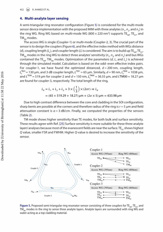
4. Multi-analyte layer sensing
A semi-triangular ring resonator configuration (figure 5) is considered for the multi-mode sensor device implementation with the proposed MIM with three analytes (n1, n2, and n3) in the ring WG. Ring WG based on multi-mode WG (800 × 220 nm2) supports TE00, TE01, and TM00 modes.
The access WG is single (coupler-1) or multi-mode (coupler-2, 3). The crucial part of the sensor is to design the couplers (figure 6), and the effective index method with WGs distance (d), coupling length (Lc), and coupler length (L) is considered. The aim is to build up TE00, TE01, TM00 modes in the ring WG to detect three analytes’ sensitivity (n1, n2, and n3) and bus WGs contained the TE00, TM00 modes. Optimization of the parameters (d, L, and Lc) is achieved through the simulated model. calculation is based on the odd–even effective index pairs. for coupler-1, we have found the optimized distanced, d = 200 nm, coupling length, LTE01c = 130 μm, and 3 dB coupler length, LTE01 = 65 μm. Similarly, d = 90 nm, LTE00c = 1038 μm, and LTE00 = 519 μm for coupler-2 and d = 150 nm, LTM00
c = 36.55 μm, and LTM00 = 18.27 μm are found for coupler-3, respectively. The total length of the ring,
Due to high contrast difference between the core and cladding in the SOI configuration, sharp bents are possible at the corners and therefore radius of the ring is r = 5 μm and field attenuation constant is α = 3 dB/cm. finally, we computed the properties of the sensors (Table 2).
TM mode shows higher sensitivity than TE modes, for both bulk and surface sensitivity. These results agree with Ref. [25] Surface sensitivity is more suitable for these three analyte layers’ analyses because most of the evanescent fields are near the surface. TE01 shows highest Q value, smaller fSR and fWHM. Higher Q-value is desired to increase the sensitivity of the sensor.
LR= L
1+ L
2+ L
3+ 3 ×
(1
3
)× (2�r) ⇒ L
R
= (65 + 519.29 + 18.27) μm + (2� × 5) μm = 633.98 μm
Access WG (395nm) Ring WG (800nm)
TE00 TE00
TE01
TM00
x
x
Coupler-1
Access WG (395nm) Ring WG (800nm)
TE00 TE00
TE01TM00
xx
Coupler-2
Access WG (395nm) Ring WG (800nm)
TE00 TE00
TE01TM00
xx
Coupler-3TM00
TE01
TE01TM00
x
x
Figure 5. proposed semi-triangular ring resonator sensor consisting of three couplers for tE00, tE01, and tm00 modes in the ring to sense three analyte layers. analyte layers are surrounded with ring Wg and water acting as a top cladding material.
Dow
nloa
ded
by [
Uni
vers
ity o
f B
irm
ingh
am]
at 1
1:58
22
May
201
6

JOuRnAl Of ElEcTROMAGnETIc WAvES AnD ApplIcATIOnS 453
5. Conclusion
Multi-mode WG-based sensing is modeled to investigate three different analyte layers. Mathematical modeling is performed to estimate the unknown RI w.r.t reference calibration database and a MIM is proposed to measure the spatially resolved RI of the three samples, which is then used for the configuration of the semi-triangular ring resonator. The perfor-mance of the proposed sensor is evaluated for fSR, fWHM, finesse, Q-factor, and sensitivity. TM mode shows higher sensitivity as compared to the TE mode, the same scenario is also observed for both bulk and surface sensing. Q-factor of TM00 is higher than TE00 mode. However, TE01 shows higher Q value and smaller fSR. In conclusion, the presented model allows the optimization and operation of multi-mode WG for multi-analyte sensing for appli-cations in biotechnology and point-of-care diagnostics.
(a1)
(a2)
(a3)
(b1)
(b2)
(b3)
Figure 6. simulated model for multi-mode sensing. (a1–3) simulation of cross section of coupler-1, 2, 3 design, and (b1–3) simulation results shows the odd and even modes.
Table 2. sensor properties for different modes.
properties Modes
TE00 TE01 TM00
free spectral range (fsr) (pm) 990.6 824.8 952.4fWHm (pm) 69.15 57.56 66.48finesse (f) 14.3254 14.326 14.326Q-factor 34,743 41,728 36,138Bulk sensitivity (nm/riu) 21.91 63.21 179.65surface sensitivity (nm/riu) 26.12 59.21 125.37surface sensitivity (nm/nm) 0.0044 0.0130 0.0602
Dow
nloa
ded
by [
Uni
vers
ity o
f B
irm
ingh
am]
at 1
1:58
22
May
201
6

454 R. AHMED ET Al.
Acknowledgements
The authors thank Dr. Matthias Jäger, Dr. Michael Stich, prof. Zahirul Hoque Mozumder, I. K. Alam Bhuiyan, Areej Badar, and prof. Dr.-Ing Klaus petermann for their valuable suggestions, comments, and fruitful discussions. Dr. Haider Butt thanks the leverhulme Trust for research funding.
References
[1] Yetisen AK, Akram MS, lowe cR. paper-based microfluidic point-of-care diagnostic devices. lab chip. 2013;13:2210–2251.
[2] Rifat AA, Mahdiraji GA, chow DM, et al. photonic crystal fiber-based surface plasmon resonance sensor with selective analyte channels and graphene-silver deposited core. Sensors. 2015;15:11499–11510.
[3] Yetisen AK, Montelongo Y, Qasim MM, et al. photonic nanosensor for colorimetric detection of metal ions. Anal. chem. 2015;87:5101–5108.
[4] Harhouz A, Hocini A. Design of high-sensitive biosensor based on cavity-waveguides coupling in 2D photonic crystal. J. Electromagn. Waves. 2015;29:659–667.
[5] Bamiedakis n, Hutter T, penty Rv, et al. pcB-integrated optical waveguide sensors: an ammonia gas sensor. J. lightwave Technol. 2013;31:1628–1635.
[6] Ahmed R, ullah DSM. Design & analysis on silicon based optical micro-ring resonator sensor device for biomedical applications at μm wavelength. cIOMp-OSA Summer Session: lasers and their Applications; 2011; china.
[7] Sun Y, fan X. Optical ring resonators for biochemical and chemical sensing. Anal. Bioanal. chem. 2011;399:205–211.
[8] Malka D, cohen M, Zalevsky Z, et al. Optical micro-multi-racetrack resonator filter based on SOI waveguide. IEEE 28th convention in Electrical & Electronics Engineers in Israel (IEEEI) 2014; Israel. p 1–5.
[9] Alavi S, Amiri I, Ahmad H, et al. Generation and transmission of 3 × 3 w-band multi-input multi-output orthogonal frequency division multiplexing-radio-over-fiber signals using micro-ring resonators. Appl. Opt. 2014;53:8049–8054.
[10] Yu X, Ma H, Jin Z, et al. Sensitive birefringent temperature sensor based on a waveguide ring resonator. Appl. Opt. 2014;53:2748–2753.
[11] Sun J, Huang M, Yang J-J, et al. A microring resonator based negative permeability metamaterial sensor. Sensors. 2011;11:8060–8071.
[12] Huang M, Yang J, Jun S, et al. Simulation and analysis of a metamaterial sensor based on a microring resonator. Sensors. 2011;11:5886–5899.
[13] Sabah c, Taygur MM, Zoral EY. Investigation of microwave metamaterial based on H-shaped resonator in a waveguide configuration and its sensor and absorber applications. J. Electromagn. Waves Appl. 2015;29:819–831.
[14] Gundogdu T, Gökkavas M, Güven K, et al. Simulation and micro-fabrication of optically switchable split ring resonators. photonics nanostruct. fundam. Appl. 2007;5:106–112.
[15] Jalas D, petrov AY, Eich M. Theory of gyrotropic ring resonators with counterpropagating modes coupling. photonics nanostruct. fundam. Appl. 2011;9:351–357.
[16] feng S, lei T, chen H, et al. Silicon photonics: from a microresonator perspective. laser photonics Rev. 2012;6:145–177.
[17] chao c-Y, Guo lJ. Design and optimization of microring resonators in biochemical sensing applications. J. lightwave Technol. 2006;24:1395–1402.
[18] ciminelli c, Dell’Olio f, conteduca D, et al. High performance SOI microring resonator for biochemical sensing. Opt. laser Technol. 2014;59:60–67.
[19] Guider R, Gandolfi D, chalyan T, et al. Design and optimization of SiOn ring resonator-based biosensors for aflatoxin M1 detection. Sensors. 2015;15:17300–17312.
[20] Rifat A, Mahdiraji GA, Sua M, et al. Surface plasmon resonance photonic crystal fiber biosensor: a practical sensing approach. IEEE photonics Technol. lett. 2015;27:1628–1631.
Dow
nloa
ded
by [
Uni
vers
ity o
f B
irm
ingh
am]
at 1
1:58
22
May
201
6

JOuRnAl Of ElEcTROMAGnETIc WAvES AnD ApplIcATIOnS 455
[21] chiu c, lay T. Ring resonator with multimode waveguide turning-mirror couplers in InGaAsp-Inp. Opt. commun. 2011;284:3590–3592.
[22] Tanushi Y, Yokoyama S. compact multimode optical ring resonators for interconnection on silicon chips. Jpn. J. Appl. phys. 2007;46:2364–2368.
[23] Ruege Ac, Reano RM. Multimode waveguides coupled to single mode ring resonators. J. lightwave Technol. 2009;27:2035–2043.
[24] Ding D, de Dood MJ, Bauters Jf, et al. fano resonances in a multimode waveguide coupled to a high-Q silicon nitride ring resonator. Opt. Express. 2014;22:6778–6790.
[25] De vos K. label-free silicon photonics biosensor platform with microring resonators [phD]. Belgium: Ghent university; 2010.
Dow
nloa
ded
by [
Uni
vers
ity o
f B
irm
ingh
am]
at 1
1:58
22
May
201
6