mode pattern analysis of gallium nitride-based laser diodes
TRANSCRIPT

Mode Pattern Analysis of Gallium Nitride-based Laser Diodes
Xiaomin Jin*a, Sean Jobea, Simeon Trieua, Benafsh Husaina, Jason Flickingera, Bei Zhangb, Tao Daib, Xiang-Ning Kangb, and Guo-Yi Zhangb
aElectrical Engineering Department, 1 Grand Avenue, California Polytechnic State University, San Luis Obispo, CA, USA, 93407-9000;
bSchool of Physics and State Key Laboratory for Artificial Microstructures and Mesoscopic Physics, Peking University, Beijing, China, 100871
ABSTRACT
In this paper, we present an analysis of gallium nitride (GaN) quantum-well (QW) laser diode (LD) by numerical simulation. Here we discuss three aspects that are crucial to our analysis. First, the transverse mode pattern is studied, and our current GaN diode laser structure is discussed with optical waveguide mode analysis. Then we compare the QW design of the laser and maximize laser modal gain. Finally, we report the influence of the electron block (e-block) layer on lasing performance of our design.
Keywords: Gallium Nitride, semiconductor laser, transverse modes
1. INTRODUCTION In the visible color spectrum, there are three primary colors: red, green, and blue, also referred to as RGB. Through the combination of these three colors, all the other colors in the spectrum can be created. For example, the combination of red and green would produce the color yellow. Current technology has found efficient ways at creating both red and green light using semiconductor technology, but the creation of blue light has not shared this immediate success. Blue light has remained the hardest light to produce efficiently from semiconductor technologies. This has been the main road block preventing highly efficient laser diodes (LDs) from replacing our current lighting technologies.
Blue violet light is close to the shortest wavelength of light in the visible spectrum. At the wavelength of 445nm, it still remains the hardest light to produce using semiconductors, because the bandgap properties of the materials needed to produce such a wavelength in semiconductors that are hard to find. In recent years, many strides have been made in studying and researching Gallium Nitrate or Gallium Nitride (GaN) as a material to yield blue light. The most progress and significant strides have been made by Dr. Nakamura, who dedicated much of his research to the chemical growth of GaN compounds. [1] Before Nakamura found a solution for growing GaN semiconductors, much of the focus for blue light semiconductors was spent on II-VI materials (where II and VI represent the group number on the Periodic Table of Elements). GaN is a III-V material and is a much harder substance to deal with because of its higher lattice defects in comparison to II-VI materials. However with Nakamura’s perilous efforts, he eventually found a technique to deposit GaN compounds and created the first GaN semiconductor. Since Nakamura has shown that GaN LED semiconductors are possible in 1995, fellow scientists across the world have worked hard to further the development and efficiency of blue light semiconductors [1].
GaN is one of the most promising materials for use in the blue and ultraviolet wavelength region. Since the room-temperature (RT) continuous-wave (CW) operation of GaN-based lasers were reported by Nakamura et al. 1996, [2] one of the important targets on the GaN LD development is to extend the operating lifetime by reducing the operation current or current density. It was pointed out that the threshold current density of GaN lasers is intrinsically higher than that of GaAs. This is because the hole effective mass of wurtzite (WZ) GaN is much heavier than that of conventional zincblende materials such as GaAs.[3] To decrease the threshold current density in GaN lasers, several approaches have been proposed. Most of the papers discuss the threshold improvement through optical gain or Quantum-well (QW) analysis. [4]-[6] The beginnings of III-V laser diode devices were very elementary in their design compared to current *[email protected]; phone 1 805-756-7046; fax 1 805-756-1458; www.ee.calpoly.edu
International Symposium on Photoelectronic Detection and Imaging 2009: Laser Sensing and Imaging,edited by Farzin Amzajerdian, Chun-qing Gao, Tian-yu Xie, Proc. of SPIE Vol. 7382, 73820O
© 2009 SPIE · CCC code: 0277-786X/09/$18 · doi: 10.1117/12.834103
Proc. of SPIE Vol. 7382 73820O-1
brought to you by COREView metadata, citation and similar papers at core.ac.uk
provided by DigitalCommons@CalPoly

designs. The GaN diodes consisted of a substrate, cladding, core, and active region. Current designs have more complex structures such as a super lattice (SL), quantum wells, and e-blocks. Using these new technologies, devices with lower laser thresholds can be created thus leading to more efficient devices. In this work, we discuss the threshold reduction on GaN QW lasers in three aspects: 1) optical waveguide design and mode analysis; 2) QW design and modal gain analysis; 3) electron- block (e-black) layer design for optimization.
2. NUMERICAL MODELING LaserMOD is an integrated software package developed by RSOFT for the design and simulation of semiconductor lasers and active photonic structures. [7] It is a fully integrated platform with a user friendly parametric CAD interface, nonuniform Delauney mesh generator, material libraries, gain and mode calculation utilities, simulation engine, standard and custom plot generation utilities, and versatile graphical viewing utilities. In short, the LaserMOD program provides the user with an immense environment in which semiconductor devices can be modeled and tested based on their user specified properties. 2.1 Optical Confinement Factor (OCF) The optical confinement factor (OCF) of a chosen mode is defined as the ratio of the energy of the chosen mode located in the active region to the total guided energy of all the modes. [8] A higher OCF for a certain mode indicates there is more energy in the active region for that mode. High energy in the active region is usually a sign that lasing is occurring. Thus, whichever mode has the highest OCF will be the lasing mode. The optical modes are determined from the solution of the Helmholtz equation via simultaneous as below, then the OCF can be calculated.
2 22
0 ,2 2 ( ( , ) ) ( , , ) 0eff m mk x y n E x y zx y
δδ
⎛ ⎞∂+ + ε − =⎜ ⎟∂⎝ ⎠
where 0 ,( , , ) ( , ) exp( )m m eff mE x y z E x y ik n z= , k0 is the free-space wave vector, and ( , )x yε is the complex dielectric constant profile of the multiplayer structure. The eigenvalues are given by the effective index neff,m. The frequency 0 0 /k c= ω of the mode is solved and is set to correspond to the quantum well band gap energy. The OCF can be thought of as the fraction of the energy of mode that is located at the active region. [9] 2.2 Mathematical Model – 8x8 Kronig-Penney (KP) Model The LaserMOD simulation software uses the Kronig-Penney (K• P) model to model the bandgap relationships of the different materials. The K• P model is based upon the splitting of allowed electron energies as the interatomic distance between atoms decreases to form a crystal. The K• P method involves quantum mechanics and a solution to Schrödinger’s wave equation. [10] For the one dimensional crystal structure, a periodic well function can be used to represent the crystal lattice structure. This is because when the potential functions of atoms are brought close together, the net potential function of the overlapping regions is similar to a periodic function. Using the specified characteristics of a periodic function for the boundary conditions for Schrödinger’s equation, a plot of the energy E as a function of wave number k can be generated, which describes the valence band, conduction band, and the allowed energy bands. However for two dimensional calculations, matrices become a necessary addition to efficiently solve Schrödinger’s wave equation. A popular method for solving E vs. k diagrams is using 8x8 matrices. Using special matrix rules and “tricks” (i.e. Helmholtz equation) these calculations can be solved with a computer program. Many programs have been written that can solve these types of mathematical problems. We chose to use RSOFT’s LaserMOD, which is a program that has a CAD interface which can easily and quickly calculate all the necessary properties of semiconductors. 2.3 The 2D nitride-based laser model A 2D nitride-based laser model is developed, which is shown in Fig.1. The simulated laser structure has five quantum-wells (QWs). A similar device was fabricated at Peking University, China. One of the project goals is to identify design flaws from the current laser design and to reduce the laser threshold. To avoid the meshing difficulties of the finite-element method, the classical Ritz simultaneous iteration is combined with an additional optimization to analyze closed
Proc. of SPIE Vol. 7382 73820O-2
arbitrary dielectric waveguides. [7] LaserMOD determines the charge distribution using Schrodinger equation. The laser simulation is based on 8x8 K• P band structure calculation and photon rate equation. The material parameters based on recent literature values and some experimental data were used. The detailed laser structure is listed in Table.1.
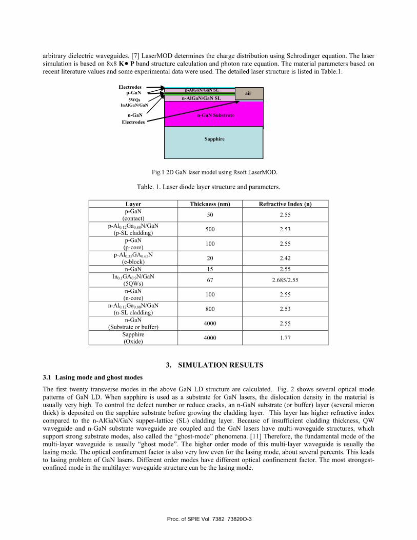
Fig.1 2D GaN laser model using Rsoft LaserMOD.
Table. 1. Laser diode layer structure and parameters.
Layer Thickness (nm) Refractive Index (n) p-GaN
(contact) 50 2.55
p-Al0.12Ga0.88N/GaN (p-SL cladding) 500 2.53
p-GaN (p-core) 100 2.55
p-Al0.35GA0.65N (e-block) 20 2.42
n-GaN 15 2.55 In0.1GA0.9N/GaN
(5QWs) 67 2.685/2.55
n-GaN (n-core) 100 2.55
n-Al0.12Ga0.88N/GaN (n-SL cladding) 800 2.53
n-GaN (Substrate or buffer) 4000 2.55
Sapphire (Oxide) 4000 1.77
3. SIMULATION RESULTS 3.1 Lasing mode and ghost modes
The first twenty transverse modes in the above GaN LD structure are calculated. Fig. 2 shows several optical mode patterns of GaN LD. When sapphire is used as a substrate for GaN lasers, the dislocation density in the material is usually very high. To control the defect number or reduce cracks, an n-GaN substrate (or buffer) layer (several micron thick) is deposited on the sapphire substrate before growing the cladding layer. This layer has higher refractive index compared to the n-AlGaN/GaN supper-lattice (SL) cladding layer. Because of insufficient cladding thickness, QW waveguide and n-GaN substrate waveguide are coupled and the GaN lasers have multi-waveguide structures, which support strong substrate modes, also called the “ghost-mode” phenomena. [11] Therefore, the fundamental mode of the multi-layer waveguide is usually “ghost mode”. The higher order mode of this multi-layer waveguide is usually the lasing mode. The optical confinement factor is also very low even for the lasing mode, about several percents. This leads to lasing problem of GaN lasers. Different order modes have different optical confinement factor. The most strongest-confined mode in the multilayer waveguide structure can be the lasing mode.
Electrodes
p-GaN
n-GaN
5WQs InAlGaN/GaN
air
n-GaN Substrate
Electrodes
Sapphire
n-AlGaN/GaN SL p-AlGaN/GaN SL
Proc. of SPIE Vol. 7382 73820O-3
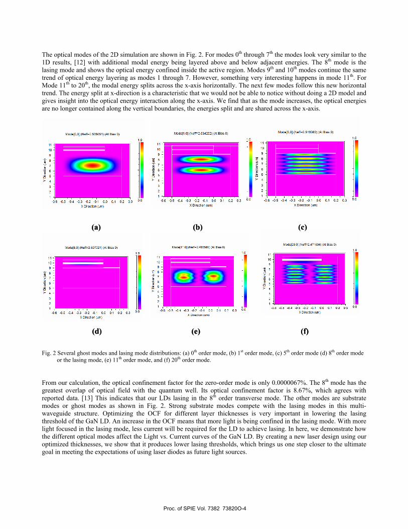
The optical modes of the 2D simulation are shown in Fig. 2. For modes 0th through 7th the modes look very similar to the 1D results, [12] with additional modal energy being layered above and below adjacent energies. The 8th mode is the lasing mode and shows the optical energy confined inside the active region. Modes 9th and 10th modes continue the same trend of optical energy layering as modes 1 through 7. However, something very interesting happens in mode 11th. For Mode 11th to 20th, the modal energy splits across the x-axis horizontally. The next few modes follow this new horizontal trend. The energy split at x-direction is a characteristic that we would not be able to notice without doing a 2D model and gives insight into the optical energy interaction along the x-axis. We find that as the mode increases, the optical energies are no longer contained along the vertical boundaries, the energies split and are shared across the x-axis. Fig. 2 Several ghost modes and lasing mode distributions: (a) 0th order mode, (b) 1st order mode, (c) 5th order mode (d) 8th order mode
or the lasing mode, (e) 11th order mode, and (f) 20th order mode. From our calculation, the optical confinement factor for the zero-order mode is only 0.0000067%. The 8th mode has the greatest overlap of optical field with the quantum well. Its optical confinement factor is 8.67%, which agrees with reported data. [13] This indicates that our LDs lasing in the 8th order transverse mode. The other modes are substrate modes or ghost modes as shown in Fig. 2. Strong substrate modes compete with the lasing modes in this multi-waveguide structure. Optimizing the OCF for different layer thicknesses is very important in lowering the lasing threshold of the GaN LD. An increase in the OCF means that more light is being confined in the lasing mode. With more light focused in the lasing mode, less current will be required for the LD to achieve lasing. In here, we demonstrate how the different optical modes affect the Light vs. Current curves of the GaN LD. By creating a new laser design using our optimized thicknesses, we show that it produces lower lasing thresholds, which brings us one step closer to the ultimate goal in meeting the expectations of using laser diodes as future light sources.
(a) (b) (c)
(d) (e) (f)
(a) (b) (c)
(d) (e) (f)
Proc. of SPIE Vol. 7382 73820O-4
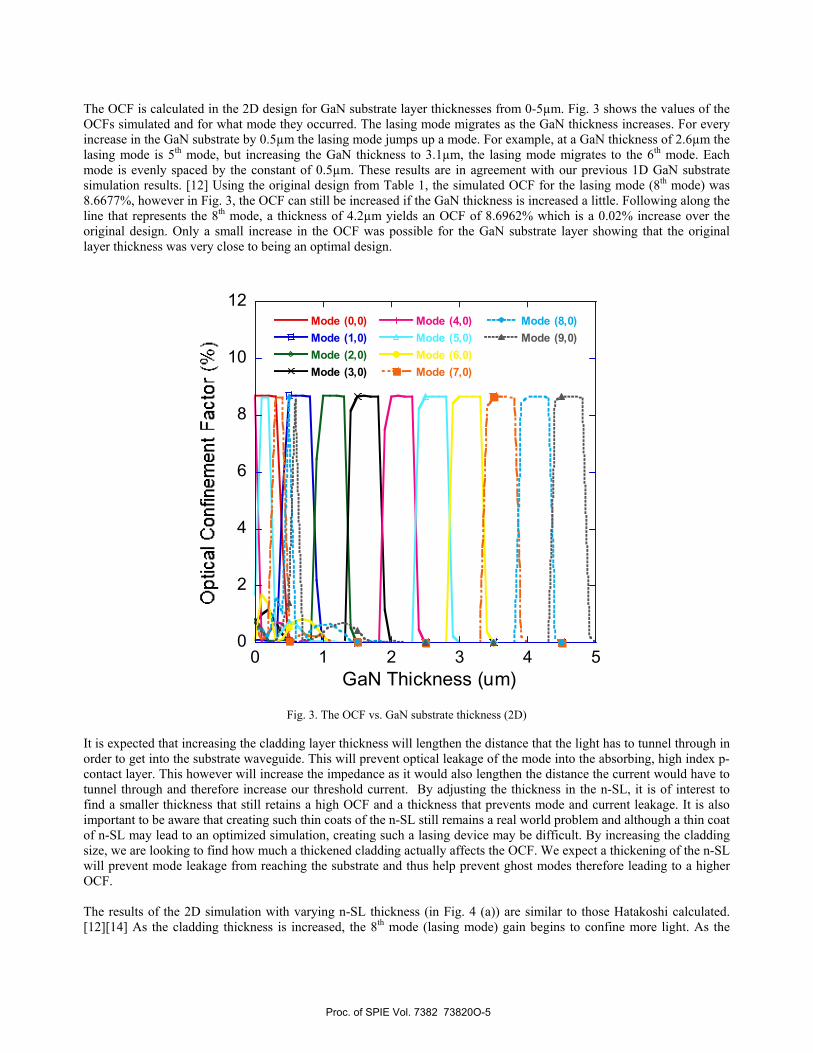
The OCF is calculated in the 2D design for GaN substrate layer thicknesses from 0-5µm. Fig. 3 shows the values of the OCFs simulated and for what mode they occurred. The lasing mode migrates as the GaN thickness increases. For every increase in the GaN substrate by 0.5µm the lasing mode jumps up a mode. For example, at a GaN thickness of 2.6µm the lasing mode is 5th mode, but increasing the GaN thickness to 3.1µm, the lasing mode migrates to the 6th mode. Each mode is evenly spaced by the constant of 0.5µm. These results are in agreement with our previous 1D GaN substrate simulation results. [12] Using the original design from Table 1, the simulated OCF for the lasing mode (8th mode) was 8.6677%, however in Fig. 3, the OCF can still be increased if the GaN thickness is increased a little. Following along the line that represents the 8th mode, a thickness of 4.2µm yields an OCF of 8.6962% which is a 0.02% increase over the original design. Only a small increase in the OCF was possible for the GaN substrate layer showing that the original layer thickness was very close to being an optimal design.
0
2
4
6
8
10
12
0 1 2 3 4 5
Mode (0,0)Mode (1,0)Mode (2,0)Mode (3,0)
Mode (4,0)Mode (5,0)Mode (6,0)Mode (7,0)
Mode (8,0)Mode (9,0)
GaN Thickness (um)
Fig. 3. The OCF vs. GaN substrate thickness (2D) It is expected that increasing the cladding layer thickness will lengthen the distance that the light has to tunnel through in order to get into the substrate waveguide. This will prevent optical leakage of the mode into the absorbing, high index p-contact layer. This however will increase the impedance as it would also lengthen the distance the current would have to tunnel through and therefore increase our threshold current. By adjusting the thickness in the n-SL, it is of interest to find a smaller thickness that still retains a high OCF and a thickness that prevents mode and current leakage. It is also important to be aware that creating such thin coats of the n-SL still remains a real world problem and although a thin coat of n-SL may lead to an optimized simulation, creating such a lasing device may be difficult. By increasing the cladding size, we are looking to find how much a thickened cladding actually affects the OCF. We expect a thickening of the n-SL will prevent mode leakage from reaching the substrate and thus help prevent ghost modes therefore leading to a higher OCF. The results of the 2D simulation with varying n-SL thickness (in Fig. 4 (a)) are similar to those Hatakoshi calculated. [12][14] As the cladding thickness is increased, the 8th mode (lasing mode) gain begins to confine more light. As the
Proc. of SPIE Vol. 7382 73820O-5

lasing mode increases in its OCF, the other modes begin to lose the light they had originally been able to confine. Thus as the cladding thickness increases all the optical energy that is available becomes confined only in the 8th mode. This is shown in Figure 4 (a). This result shows that the anti-guide-like or ghost mode behavior can be suppressed by increasing the cladding layer thickness. A thick cladding layer reduces the effect of the outer contact layers, but still is conducive to high-order modes. At the n-SL thickness of the original design (0.8µm), the OCF was 8.7128% and reaches a peak plateau on the graph at 8.7241% at a thickness of 1.4µm. The 0.01% increase in OCF requires almost doubling the thickness. Thus the best optimization for this design is simply leaving it alone. The original design yields an optimal OCF for its relative thickness. The p-SL cladding provides the same waveguide like confinement of the light as the n-SL cladding, shown in Fig. 4 (b), but it differs in that it will not be absorbing electrons like the p-SL will be. By adjusting the thickness of the p-SL, we hope to find a thickness that prevents mode leakage into the p-contact layer, yet still maintains low impedance. The adjustment of the p-SL cladding layer shows a different increase in the OCF than the n-SL plot. It is interesting to point out however that the thickening of the p-SL lattice above 0.1µm has a detrimental effect on the maximum OCF, decreasing it from a maximum of 8.7% to 8.4%. (It is important to note that it is the OCF at a different mode). Thus we find our optimal thickness for the p-SL that yields the best OCF yet remains fairly thin is at 0.1nm.
0
2
4
6
8
10
0 0.5 1 1.5
Mode (0,0)Mode (1,0)Mode (2,0)Mode (3,0)Mode (4,0)Mode (5,0)Mode (6,0)Mode (8,0)Mode (7,0)Mode (9,0)
n-AlGaN (n-SL) Thickness (um)
0
2
4
6
8
10
0 0.5 1 1.5
Mode (0,0)Mode (1,0)Mode (2,0)Mode (3,0)Mode (4,0)Mode (5,0)Mode (6,0)Mode (8,0)Mode (7,0)Mode (9,0)
p-AlGaN (p-SL) Thickness (um) (a) (b)
Fig. 4. Optical confinement vs. (a) n-SL and (b) p-SL thickness The GaN core layer in the 2D simulation has a refractive index greater than the surrounding cladding layers to reflect the light back towards the active region. A thicker core layer can lead to more optical losses due to the large area the light has to travel. Thus choosing an optimal core layer thickness is important in creating the most efficient laser diode. The OCF is plotted in Fig. 5 for n-GaN layer thicknesses of 0-1µm. The OCF peaks at 8.7027% with an n-GaN thickness of 0.075µm. This is a 0.224% increase in the OCF from 8.6762% when a 0.1µm layer is used. Thus by using a thinner layer of n-GaN core layer, a better optical confinement can be achieved. Fig. 5 shows a constant decrease in the OCF as the n-GaN thickness is increased and the lasing mode migrates to lower modes. The same simulation was run for the p-GaN core layer and the results of the OCF vs. p-GaN thickness are also plotted in Fig.5. The maximum OCF is achieved for small thin layers of p-GaN. The OCF peaks with 8.8664% at a thickness of 0.05µm. This is a 0.2% increase over the original design when the p-GaN was 0.1µm thick and had an OCF of 8.6762%. Similar to the n-GaN core layer, a thinner layer creates better optical confinement.
Proc. of SPIE Vol. 7382 73820O-6

0
2
4
6
8
10
0 0.2 0.4 0.6 0.8 1
Mode (0,0)Mode (1,0)Mode (2,0)Mode (3,0)Mode (4,0)Mode (5,0)Mode (6,0)Mode (7,0)Mode (8,0)Mode (9,0)
n-GaN Thickness (um)
0
2
4
6
8
10
0 0.2 0.4 0.6 0.8 1
Mode (0,0)Mode (2,0)Mode (1,0)Mode (3,0)Mode (4,0)Mode (7,0)Mode (5,0)Mode (6,0)Mode (8,0)Mode (9,0)
p-GaN Thickness (um) (a) (b)
Fig. 5. Optical confinement factor vs. (a) n-GaN and (b) p-GaN layer thickness
Fig. 6 The GaN laser simulation for (a) far field pattern, (b) light output versus current, (c) model gain of all the transverse
mode, and (d) model gain of lasing mode only.
(a) (b)
(c) (d)
0
0.2
0.4
0.6
0.8
1
1.2
-60 -40 -20 0 20 40 60
lasing mode5 modes8 modes10 modes20 modes
Y driection (degree)
-8
-6
-4
-2
0
2
2.85 2.9 2.95 3 3.05 3.1
5 modes8 modes10 modes20 modes
Energy (eV)
0
10
20
30
40
50
0
0.5
1
1.5
2
2.5
0 20 40 60 80 100
Lasing mode20 modes
Current (mA)
-600
-500
-400
-300
-200
-100
0
100
2.9 2.95 3 3.05 3.1
Lasing Mode
Energy (eV)
Proc. of SPIE Vol. 7382 73820O-7

To prove the optical mode design can improve CW GaN LD operation, the threshold, optical power, quality of far-filed, and optical gain should be evaluated, which are the most important issues and represents the laser performance. For examples, in 2002, Tojyo et al reported a kink free output of over 100mW. In 2005 Schwarz et al reported near- and far-field study of GaN LDs. [15] In 2007, Laino et al reported results on substrate mode study. And in 2006, [16] Witzigmann et al reported optical gain analysis. [17] Here we calculate the far field pattern, model gain, optical output, and threshold with only lasing mode (the 8th mode), and all the transverse modes to demonstrate the ghost mode effects, shown in Fig. 6. For the far field simulation, we normalized the optical pattern to the peak value for comparison. In the figures, lasing mode represents the 8th order mode only simulation, “x modes” means “the first x transverse modes”. The “8 modes” means modes 0 to 7. For the case of “5 modes” or “8 modes”, there is no lasing mode included in the calculation and LD does not reach threshold for lasing. For the “8 modes”, “10 modes”, and “20 mode” cases, little modal gain is obtained from laser, which is about 10-5 cm-1. Therefore the light output is only about 10-8 mW. If we calculate those results with only 8th order lasing mode, the laser can reach a peak gain of about 25cm-1, lasing output is about 40mW at 80mA, and threshold is about 19mA. According to our optical field analyses, the strong ghost-modes compete with lasing-mode in GaN Laser, which can prevent the laser from lasing. For the worst case, if the waveguide structure supports strong ghost-modes, the GaN laser would not operate even though the active region quantum well is perfect. Design of the optical waveguide for GaN laser system is very important to achieve efficient lasing condition. In this work, we find that the n-GaN substrate thickness is the major factor influencing the transverse mode pattern. In a related work, [12] we optimized the optical waveguide structure, which limits the ghost modes, and maximizes confinement factor of the laser structure, in order to reduce lasing threshold. 3.2 The QW analysis and model gain simulation
Quantum wells are designed to trap electrons in a 2-D environment. The wells are designed to have a particular bandgap energy related to the wavelength of light emitted by the laser diode. The quantum well allows the electrons to gather more densely in the well than they would elsewhere. It is easy to think of it as though the well is drawing electrons towards it then trapping them. (In fact, it isn’t so much that the wells are drawing electrons to them and away from the other parts of the semiconductor; instead electrons keep falling into the well, and the well becomes saturated and full that it seems as though the well is attracting electrons.) This packs more electrons in the active region and allows more electrons to jump the bandgap thereby releasing a photon. The size of the well must be on order of the wavelength of light hoping to be produced. Each well is created by creating a thin layer (the well) and surrounding it by thicker layers of a different material. Thus for a multi quantum well (MQW) design, there would be alternating layers of bulk and active layers. The well layer is made from the normal active layer material with a lower refractive index then the surrounding bulk layers. This in a sense is like having many tiny optical cavities that interact with photons at the quantum level. It can be shown that the more quantum wells in a semiconductor, the larger the threshold current becomes. This is because when there are more wells for the electrons to fall into, a higher current is necessary to provide the quantum wells with enough electrons to maintain saturation which in turn is the foundation of lasing. [18]
Quantum wells have many advantages in the design a laser diode structure. First, by using QWs, one has the freedom to design the transition energies, which ultimately determines the wavelength of light that leaves the active region in the form of spontaneous emission. Second, since QWs have a small volume, the free carrier concentration in the QW is high and at high free carrier concentrations non-radiative deep-level transitions are less likely thus yielding a high radiative efficiency. Third, due to the small size of the quantum wells, the carrier density required to achieve population inversion (i.e., high carrier density in the conduction band, compared with the valence band) is small and therefore the threshold current density of QW structures is low. And finally, the surface recombination is less likely, which making surface recombination less important in the study of QWs. [18] The structure we simulated here has a wide contact with a uniform current injection. The number of QWs, the QW width, and composition fluctuations play central roles in the optimization of GaN light-emitting diodes (LEDs) and LDs. [4]-[6] [17] Our simulation here considers number of QWs and composition. We choose lasing mode only simulation, without considering optical mode variation for simplification. The band structure of QWs is computed using k• p method, which includes coupling effects for the heavy-hole, light-hole, and the crystal-field split hole dispersion. The QW is InxGa1-xN/GaN. The width is 5nm/7nm (well/barrier), and x=0.1. From Fig. 7(a), the peak modal gain increases from 17 cm-1 for 1QW to 3.7 cm-1 for 3QWs. Then it reduces to 29.1cm-1 and 25.3cm-1 for 4 QWs and 5 QWs. The 3 QWs Case provides the highest gain peak. This agrees with the light optical power-current (LI) curve simulation in Fig. 7(b). The carrier densities are inhomogeneous among the quantum wells. [19] The optical gain is generated only in three
Proc. of SPIE Vol. 7382 73820O-8

QWs on the p-side for our case. The QWs on the n-side act as absorption layers. Therefore, for the LDs with more than three QWs, the peak gain reduces, which results the light output slope (or quantum efficiency) reduction in LI plots. From the threshold and gain simulation, it is important to decrease the number of wells. Single quantum well GaN LD is the best design structure, however it has a lot of fabrication challenges. Besides the above gain simulation, we have varied structural parameters and calculate the threshold currents of lasers. The threshold current increases as QW number increases and decreases with InxGa1-xN/GaN composition x, as shown in Fig. 8. Higher “In” composition in the QW will obtain higher gain, however it has to be balanced with drawback of the lattice mismatch and deterioration in material quality for a larger “In” fraction. For 5 QW case, the threshold current shows little composition dependence, while x varies from 0.08 to 012. This will provide good threshold stable point with fabrication tolerance.
Fig.7 (a) Model gain and (b) LI curve simulation for In0.1 Ga 0.9N/GaN single-QW and MQWs without e-block.
Fig. 8 Threshold current for different QW composition x: InxGa1-xN/GaN and QW number.
0
5
10
15
20
0 5 10 15 20 25 30
1QW2QW3QW4QW5QW6QW
Current (mA)
(a) (b)
-60
-40
-20
0
20
40
2.9 2.95 3 3.05
1QW2QW3QW4QW5QW6QW7QW
Energy (eV)
0
5
10
15
20
0 5 10 15 20 25 30
1QW2QW3QW4QW5QW6QW
Current (mA)
(a) (b)
-60
-40
-20
0
20
40
2.9 2.95 3 3.05
1QW2QW3QW4QW5QW6QW7QW
Energy (eV)
Proc. of SPIE Vol. 7382 73820O-9
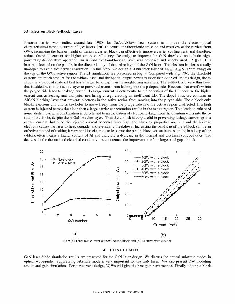
3.3 Electron Block (e-Block) Layer
Electron barrier was studied around late 1980s for GaAs/AlGaAs laser system to improve the electro-optical characteristics/threshold current of QW lasers. [20] To control the thermionic emission and overflow of the carriers from QWs, increasing the barrier height or design a carrier block can effectively improve carrier confinement, and therefore, reduce threshold current for higher emission efficiency. Recently, to improve the GaN threshold and obtain high-power/high-temperature operation, an AlGaN electron-blocking layer was proposed and widely used. [21][22] This barrier is located on the p–side, in the direct vicinity of the active layer of the GaN laser. The electron barrier is usually un-doped to avoid free carrier absorption. In this work, we design a 20nm thick layer of Al0.35Ga0.65N (15nm away) on the top of the QWs active region. The LI simulations are presented in Fig. 9. Compared with Fig. 7(b), the threshold currents are much smaller for the e-block case, and the optical output power is more than doubled. In this design, the e-Block is a p-doped material that has a larger band gap than its neighboring materials. The e-Block is a very thin layer that is added next to the active layer to prevent electrons from leaking into the p-doped side. Electrons that overflow into the p-type side leads to leakage current. Leakage current is detrimental to the operation of the LD because the higher current causes heating and dissipates non-lasing energy creating an inefficient LD. The doped structure contains an AlGaN blocking layer that prevents electrons in the active region from moving into the p-type side. The e-block only blocks electrons and allows the holes to move freely from the p-type side into the active region unaffected. If a high current is injected across the diode then a large carrier concentration results in the active region. This leads to enhanced non-radiative carrier recombination at defects and to an escalation of electron leakage from the quantum wells into the p-side of the diode, despite the AlGaN blocker layer. Thus the e-block is very useful in preventing leakage current up to a certain current, but once the injected current becomes very high, the blocking properties are null and the leakage electrons causes the laser to heat, degrade, and eventually breakdown. Increasing the band gap of the e-block can be an effective method of making it very hard for electrons to leak onto the p-side. However, an increase in the band gap of the e-block often means a higher content of Al and therefore a decrease in the thermal and electrical conductivities. The decrease in the thermal and electrical conductivities counteracts the improvement of the large band gap e-block.
Fig.9 (a) Threshold current with/without e-block and (b) LI curve with e-block.
4. CONCLUSION GaN laser diode simulation results are presented for the GaN laser design. We discuss the optical substrate modes in optical waveguide. Suppressing substrate mode is very important for the GaN laser. We also present QW modeling results and gain simulation. For our current design, 3QWs will give the best gain performance. Finally, adding e-block
(a) (b)
4
6
8
10
12
14
16
18
20
1 2 3 4 5 6
No-e-blockWith-e-block
QW number0
10
20
30
40
50
60
0 5 10 15 20 25 30
1QW with e-block2QW with e-block3QW with e-block4QW with e-block5QW with e-block6QW with e-block
Current (mA)
Proc. of SPIE Vol. 7382 73820O-10
layer on the top of quantum-well active layer will reduce threshold by about 30% to 40%.
ACKNOWLEDGEMENT This project is supported by Department of the Navy, Office of Naval Research, under Award # ONR 6-N00014-07-1-1152 in 2008, Award # ONR 7-N000140811209 in 2009, USA; “ChunHui” exchange research fellow 2008, Educational Department, China; 973 program-National Basic Research Program of China (2007CB307004); High Technology program (863-2006AA03A113) and National Nature Science Foundation of China (60276032, 60577030 and 60607003).
REFERENCES
[1] Nakamura, S., [The Blue Laser Diode], 2nd ed., Springer, (1997). [2] Nakamura, S., Senoh, M., Nagahama, S., Iwasa, N., Yamada, T., Matsushita, T., Sugimoto, Y. and Kiyoku, H.,
“Room-temperature continuous-wave operation of InGaN multi-quantum-well structure laser diodes,” Appl. Phys. Lett. 69 (26), 4056-4058, (1996).
[3] Suzuki, M., Uenoyama, T. and Yanase, A., “First-principles calculations of effective-mass parameters of AlN and GaN,” Phys. Rev. B 52 (11), 8132-8139, (1995).
[4] Suzuki, M. and Uenoyama, T., “Strain effect on electronic and optical properties of GaN/AlGaN quantum-well lasers,” J. Appl. Phys. 80(12), 6868-6874, (1996).
[5] Ohtoshi, T., Niwa, A. and Kuroda, T., “Dependence of optical gain on crystal orientation in wurtzite–GaN strained quantum-well lasers,” J. Appl. Phys. 82(4), 1518-1520, (1997).
[6] Domen, K., Horino, K., Kuramata, A. and Tanahashi, T., “Optical gain for wurtzite GaN with anisotropic strain in c plane,” Appl. Phys. Lett. 70(8), 987-989, (1997).
[7] LaserMOD v2.0 User Guide, RSOFT Design Group, Inc., New York, (2004). [8] Wakita, Koichi, [Semiconductor Optical Modulators], Springer, New York City, (1998). [9] Botez, D., “Analytical approximation of the radiation confinement factor for the TE0 mode of a double
heterojunction laser,” IEEE J. Quantum Electronics QE-14 (4), 230–232, (1978). [10] Neamen, Donald A., [Semiconductor Physics and Devices: Basic Principles], 3rd ed., McGraw Hill, New York City,
(1992). [11] Smolyakov, G. A., P. G. Eliseev, and M. Osinski., “Effects of resonant mode coupling on optical Characteristics of
InGaN-GaN-AlGaN lasers,” IEEE J. Quantum Electronics 41(4), 517-524, (2005). [12] Jin, X., Zhang, B., Dai, T. and Zhang, G., “Effects of Transverse Mode Coupling and Optical Confinement Factor
on Gallium Nitride-Based Laser Diode,” The Institute of Physics: Chinese Physics, 17(4), 1274-1278, (2008). [13] Einfeldt, S., S. Figge, Bottcher, T. and Hommel, D., “Coupling of optical modes in GaN-based laser-diodes,”
Physica Status Solidi(c). 0(7), 2287-2291, (2003). [14] Hatakoshi, G. I., Onomura, M., Saito, S., Sasanuma, K. and Itaya. K., "Analysis of Device Characteristics for InGaN
Semiconductor Lasers." Japanese Journal of Applied Physics 38(16), 1780-1785, (1999). [15] Schwarz, U.T., Pindl, M., Wegscheider, W., Eichler, C., Scholz, F., Furitsch, M., Leber, A., Miller, S., Lell, A.
and Harle, V., “Near-field and far-field dynamics of (Al,In)GaN laser diodes,” Appl. Phys. Lett. 86(16), 161112(3pages), (2005).
[16] Laino, V, Roemer, F., Witzigmann, B., Schwarz, U.T., Fischer, H., Feicht, G., Wegscheider, W., Rumbolz, C., Lell, A. and Harle, V., “Substrate Modes of (Al,In)GaN Semiconductor Laser Diodes on SiC and GaN Substrates,” IEEE. J. Quantum Electronics 43(1), 16-24, (2007).
[17] Witzigmann, B., Laino, V., Luisier, M., Schwarz, U.T., Fischer, H., Feicht, G., Wegscheider, W., Rumbolz, C., Lell, A. and Harle, V., “Analysis of temperature-dependent optical gain in GaN-InGaN quantum-well structures,” IEEE. Photon. Tech. Lett. 18(15), 1600-1602, (2006).
[18] Schubert, E. F. [Light-Emitting Diodes], 2nd ed., Cambridge University Press, (2006). [19] Domen, K., Soejima, R., Kuramata, A., Horino, K., Kubota, S. and Tanahashi, T., “Interwell inhomogeneity of
carrier injection in InGaN/GaN/AlGaN multiquantum well lasers,” Appl. Phys. Lett. 73(19), 2775-2777, (1998). [20] Blood, P., Fletcher, E.D., Woodbridge, K., Heasman, K.C. and Adams, A.R., “Influence of the barriers on the
temperature dependence of threshold current in GaAs/AlGaAs quantum well lasers,” IEEE J. Quantum Electronics 25(6), 1459-1468, (1989).
Proc. of SPIE Vol. 7382 73820O-11

[21] Wiedmann, N., J. Schmitz, K. Boucke, N. Herres, J. Wagner, M. Mikulla, R. Poprawe, G. Weimann. , “Band-edge aligned quaternary carrier barriers in InGaAs-AlGaAs high-power diode lasers for improved high-temperature operation,” IEEE J. Quantum Electronics 38(1), 67-72, (2002).
[22] Tu, R.-C., Tun, C.-J., Pan, S.-M., Chuo, C.-C., Sheu, J.K., Tsai, C.-E., Wang, T.-C. and Chi, G.-C., “Improvement of near-ultraviolet InGaN-GaN light-emitting diodes with an AlGaN electron-blocking layer grown at low temperature,” IEEE Photon. Tech. Lett. 15(1), 1342-1344, (2003).
Proc. of SPIE Vol. 7382 73820O-12