model 2109 status encoder - signalcrafters manual.pdfmodel 2109 status encoder table of contents...
TRANSCRIPT

USER’S MANUAL
MODEL 2109STATUS ENCODER
SIGNALCRAFTERS TECH, INC.57 Eagle Rock Avenue
East Hanover, NJ 07936-3144(800) 523-5815
or(973) 781-0880
www.signalcrafters.com

Model 2109 Status Encoder
Table of Contents
Section Title Page 1 General, Functional 1 2 Inspection 4 3 Mounting 4 4 Installer Connections 5 5 Set-Up 8 6 Testing 16 7 Specifications 18 8 Options 21 9 Warranty 21 10 Circuit Description 21 11 Parts List 24 12 Outline Drawings 27 13 PC Board Assemblies 28 14 Schematics 33 1. GENERAL, FUNCTIONAL 1.1 This manual provides circuit description, installation procedures, basic testing information, and parts list for the Model 2109 Status Encoder. 1.2 The 2109 is a Wescom 400 – Tellabs Type 10 compatible card which is capable of simultaneously monitoring up to twelve inputs. It also provides a single relay control output – which may be expanded to a total of 65 with the addition of multiple relay expansion cards (2450, 2451, 2452). The 2109 contains both a DTMF encoder and decoder. 1.3 The twelve status inputs are optically isolated current sensors. Each input is dip-switch settable as N.O. (an alarm turns current ON) or N.C. (an alarm turns current OFF), and dip-switch settable to cause an alarm or not. To monitor dry contacts, connect each input in series with its contact and a source voltage – normally the source powering the 2109. 1.4 The 2109 may be used in either polling or self-initiate systems (change of state). The integrity of low activity self-initiate systems can be verified via a built-in 1 to 99 hour report timer, settable from the master station. 1.5 The 2109 is intended for use over virtually any voice-grade audio path including leased phone lines, cellular radio, UHF/VHF radio, or microwave. PSTN dial-up and cellular circuits may also be used with the addition of an FCC registered coupler and setting the appropriate dip-switches. 1.6 Typical applications for the 2109 fall into two general categories: 2
1. Reporting to a Model 2000 PC Master or Model 2106/2107 Base Master driving a Model 2401A printer.
2. Working in combination with another remotely located 2109 programmed as a complementary ACK/NAK pair, for SCADA extension.
1.7 The 2109 is the core product of the Lucas Ledex Sub-SCADA systems. The 2109 is DTMF code compatible with the following Lucas Ledex equipment:
2450, 2451, 2452 (and older 2212R) Relay Expanders 2110 Analog Encoder and 2110E Analog Expander Older Status Encoders 2104 and 2108 2211 and 2204 Controllers
1.8 Encoder Functional Description 1.81 For Interrogate Mode Only, set dip-switch 2 to ON. Paragraph 1.8x descriptions apply only to the 2109 programmed for both Self-Initiate and Interrogate Mode (mode dip-switches 2, 3 and 4 OPEN): 1.82 STACK OPERATION – The 2109 incorporates a 7 level stack (buffer) which stores data until it can be transmitted. Each level contains Alarm/Status information for all 12 inputs. Operation of the stack is first in, first out. Therefore, multiple sequential input changes will be transmitted in the order that they occurred. If the stack fills up in a highly active system, new data will be discarded, preserving those changes which started the sequence of events; yet upon “catching up,” the encoder will send the most recent data. With dip-switch 3 ON (ACK/NAK), the stack is only 2 levels. 1.83 C.O.R. OPERATION – This opto-coupled input inhibits DTMF transmissions while active. Data on the stack and subsequent changes will be saved and transmitted when C.O.R. is released. C.O.R. (carrier operated relay) logic is provided by a companion radio receiver. The C.O.R. may be programmed for N.O. or N.C. operation. 1.84 MULTIPLE SEND OPERATION – If s stem requirements are such that multiple sends are required, changes will be put on the stack and transmitted at the next send interval. If no changes occur between sends, the encoder will transmit the present status. 1.85 OPTO-COUPLER SCANNING – In normal operation all 12 opto-coupler inputs are scanned for a change of state. If a change occurs and remains changed for the recognition time, it will be acknowledged. Recognition times are program wire programmable for 100, 200, 400 or 800 milliseconds. If the input reverts back to its original state before recognition time, it will be ignored. A qualified change of state causes transmission of a DTMF burst containing the status of all 12 inputs. These conditions will inhibit immediate transmission:
a. Mode dipswitches 2, 3 or 4 ON. b. There is data on the stack (buffer) which must be sent first. c. C.O.R. (Carrier Operated Relay) Inhibit is active. d. Unit is decoding incoming DTMF (interrogation, control relay command, etc.) e. The encoder has been configured fir MULTIPLE SEND operation and is in the
‘wait period’ between transmissions. 3

1.9 DECODER FUNCTIONAL DESCRIPTION – The following functions are remotely controlled via DTMF.
1.91 INTERROGATION – To interrogate a 2109 programmed for address 1001, send: 1 0 0 1 #. It will then transmit Alarm/Status data for its 12 inputs. 1.92 CONTROL RELAYS – If mode dip-switch 3 is OPEN, the 2109’s control relay (K2) provides 2 form-C contacts, which can be latched on; or pulsed on for 100 milliseconds, then off. The 2109 will echo the DTMF command, confirming the audio path. Optional relay card(s) can be added to provide up to 64 additional relays. The relay command is a six digit DTMF string: four address digits, one function digit, and one digit specifying the relay. Function * latches it on; # pulses it on, then latches it off. DTMF 1 thru 8 represent relays 1 through 8 on the optional relay cards; either 0 or 9 represents K2 on the 2109; “A” represents all 9 relays. At site 1001: DTMF Action 1001*1 relay card K1 latches on 1001*2 relay card K2 latches on 1001*0 2109 K2 latches on 1001#A relay card K1 thru K8 and 2109 K2 pulse on for 100 ms, then latch off 1001#9 2109 K2 pulses on for 100 milliseconds 1001#1 relay card K1 pulses on for 100 milliseconds To control more than one relay card, program the fourth (yellow) address wire to DTMF * (see paragraph 5.331). If mode dip-switch 3 is ON, the slave card relays are controlled by a companion 2109 after an exchange of several messages (ACK/NAK mode). This is often used to extend the contact inputs and control outputs of a SCADA system. ACK/NAK (verify before execute) systems use a pair of 2109’s slaved to each other monitoring contact closures at one location and replicating them at the other. Relay card(s) automatically follow the inputs of the companion 2109. Operation involves a sequence of automatically exchanged messages for use in critical control operations (more on ACK/NAK in paragraph 5.332). 1.93 REPORT TIMER – The 2109 can send an automatic status report at a programmed time interval. Intervals from 1 to 99 hours can be selected (in 1 hour increments). Both the time until first send and the interval between sends are programmable. This is a step operation. 1.931 The following examples show how the report timer is programmed. To activate the report timer 3 hours from now, with a repeat interval of 6 hours, 1.) Send the DTMF string: 1 0 0 1 D 0 6. The remote 2109 at site 1001 echoes the same string, indicating that a 6 hour timer has started. 2.) Next, send: 1 0 0 1 * 0 3. The first report will occur in 3 hours, with subsequent reports at 6 hour intervals. 1.932 To interrogate the report timer interval at site 1001, send DTMF string: 1 0 0 1 D. The remote 2109 echoes the following DTMF string: 1 0 0 1 D 0 6, indicating an interval of 6 hours. 4

1.933 To request the time-until-next-report at site 1001, send the following string: 1 0 0 1 *. The remote 2109 will echo: 1 0 0 1 * 0 3, indicating 3 hours until the next report. 1.934 To disable the report timer at site 1001, send the DTMF string: 1 0 0 1 D 0 0. The remote 2109 at site 1001 echos the same DTMF string, indicating that report timer is disabled (set to 0). If this 2109 is interrogated for duration, it will respond 1 0 0 1 D 0 0, indicating report timer is disabled. (The response to a request for time-until-next-report will be: 1 0 0 1 * 0 0, also indicating that the timer is disabled. 1.935 Under normal circumstances, increments of hours (1 to 99) are adequate. However, for setup, testing, or monitoring a communications path, a much shorter interval may be useful. The 2109 can be set to ‘ten second’ increments. That is, intervals 1 to 99 become 10 to 990 seconds. To set 10 second mode, send: 1 0 0 1 D D *. The 2109 will echo the string.
To set a report interval of 30 seconds, send: 1 0 0 1 D 0 3
To return to 1 hour increments, send: 1 0 0 1 D D C
To interrogate the increment, send: 1 0 0 1 D D. If 10 second increments, the 2109 will echo: 1 0 0 1 D D * If 1 hour increments, it will echo: 1 0 0 1 D D C
The 2109 defaults to ‘hours’ on power-up. 1.94 AUTOANSWER/AUTODIAL – The AutoAnswer/AutoDial parameters (number of rings, answer seize time, telephone number, OFF-hook time, ON-hook time, etc.) are stored in the non-volatile memory (EEPROM). AutoAnswer/AutoDial: Dip-switch 4 arms AutoAnswer/AutoDial operation – AND the ability to read from and write into the EEPROM via DTMF signaling. See paragraph 5.333 for detailed set-up. 2. INSPECTION 2.1 Inspect the equipment thoroughly as soon as possible after delivery. Damages should be reported immediately to the shipping carrier. 2.2 Signalcrafters equipment is identified by a part number and suffix label located on the unit and a model number on the front panel silkscreen or label. 3. MOUNTING 3.1 The 2109 card is designed to be mounted in existing Wescom 400 or Tellabs Type 10 shelves or apparatus cases. A low profile card pull handle is standard. The 2109 may be specified with 24 or 48 VDC input power so the unit may be powered from the power supply buss already in place. A 12 VDC model is also available with its power input on different card-edge fingers.
5

3.2 The 2109 may also be mounted in a slot of the Lucas Ledex Model 2504 Remote Station Assembly. The Model 2504 provides a NEMA enclosure and mounting shelf for up to five cards; it can be equipped with an optional PSTN coupler, radio link, battery and charger. 4. INSTLLER CONNECTIONS 4.1 Since the 2109 is a plug-in card, connections are normally made to the wire wrap connections already present in the card shelf or apparatus case. The pre-wired Lucas Ledex 2504 Remote Station Assembly provide screw terminals for customer connections. 4.2 The chart below lists installer connection information. The numbers represent the appropriate card-edge finger connection.
STATUS ENCODER CONNECTOR PINOUT Tx Audio Lo (Common) 1 2 C K1-2 (Tx Audio Out Hi)
K1-2 (Tx Audio In Hi) NC 3 4 NC K1-1 (Keying) K1-1 (Keying) C 5 6 NO K1-1 (Keying)
K2-1 (Auxiliary) NC 7 8 C K2-1 (Auxiliary) K2-1 (Auxiliary) NO 9 10 NC K2-2 (Auxiliary) K2-1 (Auxiliary) C 11 12 NO K2-2 (Auxiliary)
- for Input #12 13 14 + for Input #12 - for Input #11 15 16 + for Input #11 + DC Common 17 18 - for COR Input - for Input #10 19 20 + for Input #10 - for Input #9 21 22 + for Input #9 - for Input #8 23 24 + for Input #8 - for Input #7 25 26 + for Input #7 - for Input #6 27 28 + for Input #6 - for Input #5 29 30 + for Input #5 - for Input #4 31 32 + for Input #4 - for Input #3 33 34 + for Input #3
-24/-48 VDC Power In 35 36 + for COR Input - for Input #2 37 38 + for Input #2 - for Input #1 39 40 + for Input #1
Positive Source 41 42 Negative Source 43 44 - 5 VDC OUT 45 46
- for External Trigger In 47 48 + for External Trigger In Ring Detect 49 50 Unswitched Tx Audio Out Hi Relay Count 51 52 Relay Reset 53 54
Tx DTMF In Lo 55 56 Rx DTMF In Hi Power connections depend on which voltage unit you have. For 12 VDC (2109-XXXX1): + common 41 -12 VDC 43 For 24 VDC (2109-XXXX2): + common 17
6 -24 VDC 35

For 48 VDC (2109-XXXX4): + common 17 -48 VDC 35 4.21 Radio Connection Most radios use a +12 VDC power supply. Therefore, all cards in a 2504(A) system should be 11 VDC to 16.5 VDC. Using a 2109-XXXX1 would require the following connections: Audio Common 1 RX Audio In 56 Tx Audio Out 2 TX Audio In (mike) 3 Push To Talk 6 For negative PTT, jumper 5 to 43 For positive PTT, jumper 5 to 41 Daisy chain 1 to 43 to 55. NOTE: Signalcrafters encoder cards have front panel screwdriver settable pots for radio deviation adjustment. See paragraph 5.53. 4.22 2-Wire PSTN (Dial-up) Connection To connect a 2109 to the public switched telephone network (PSTN) requires an FCC Part 68 registered coupler. Connection of a Lucas Ledex B02944 PSTN Line Coupler to the 2109 follows: Coupler 2109 card-edge fingers Green 1 and also to 55 Blue 2 and also to 56 Black 5 and also to 54 White 6 Red 41 Orange 49 4.23 2-Wire Dedicated Leased Line Connection Audio Tip 2 Audio Ring 1 Connect a wire from 2 to 56; and a wire from 1 to 55 4.24 4-Wire Dedicated Leased Line Connection TX Out Tip 2 TX Out Ring 1 RX In Tip 56 RX In Ring 55
7

8

5. SET-UP 5.1 The 2109 has numerous field-programmable features. These are changed by two methods: dip-switch settings and program wires. The unit must be properly programmed before placing it into service. The illustration in this section shows how the unit is programmed when shipped. Use the information which follows to tailor these features to your application. 5.2 PROGRAM WIRES 5.21 If a target program pin is occupied, place the program wire on the repeat pin of the occupying wire; if it is also occupied, follow the “daisy chain” to the next available pin.
CAUTION: Exercise care when moving program wires. Do NOT pull from the insulator sleeve. A small screwdriver or similar tool can be used to “lift” the program wire from the pin. Pry from very close to the pin.
5.22 For user convenience, ALL program wires and dipswitches are accessible without separating the bards. Most field-programmable features are located on the top board – except impedance and COR operation, which are located near the edge of the bottom board. 5.23 ADRESS – Wires A1 through A4 determine the address for both transmit and receive functions. Each digit may be chosen from the sixteen DTMF characters. Any unused digit will be interpreted as a “DTMF D”. Connect wires A1 through A4 to the character pins corresponding to the selected address. For example, the 2109 is shipped programmed for address 1001: BROWN to character 1 (through a daisy chain of other program wires), RED to character 0, ORANGE to RED’s repeat pin, YELLOW to BROWN’s repeat pin. To control more than one relay card, program the fourth (yellow) address wire to DTMF * (see paragraph 5.331). 5.24 RECOGNITION TIME – Status inputs must be stable for this time duration before a change of state is recognized as valid. Connect the GRAY wire to 100, 200, 400, or 800 milliseconds pin – shipped on 800 milliseconds. 5.25 TRANSMIT DELAY – The time between closure of the transmit relay and the beginning of DTMF tone transmission. Connect the VIOLET wire to either the 100, 200, 400, or 800 milliseconds pin – shipped on 400 milliseconds. 5.26 NUMBER OF SENDS -- In self-initiate (report on change of state) mode of operation, the unit can send from 1 to 9 times. Connect the GREEN wire to the selected number – shipped on 1. 5.27 REPEAT SEND INTERVAL – If more than one send is selected, program the time interval between sends, by connecting the BLUE wire per table on next page:
9

Interval Interval
In seconds Character pin In seconds Character pin 5 1 (As shipped) 35 7
10 2 40 8 15 3 45 9 20 4 50 0 25 5 55 * 30 6 60 #
5.28 OUTPUT IMPEDANCE – The output impedance of the encoder can be either 600 or 900 Ohms. Connect the GREEN wire on the LOWER printed circuit board to either 600 or 900. Shipped programmed to the 600 Ohms. 5.29 CARRIER OPERATED RELAY (COR) – This input inhibits DTMF transmission during channel activity. The COR can be either Normally Open (N.O.) or Normally Closed (N.C.). Connect the BLACK wire on the LOWER printed circuit board to ‘N.O.’ or ‘N.C.’ as required per the following table:
Black Wire Transmission Inhibited By N.O. (As Shipped) Presence of COR input current. N.C. Absence of COR input current.
5.3 DIP-SWITCHES 5.30 INPUT STATE: SWITCH SW102 The twelve status inputs may be either Normally Open (form-A) or Normally Closed (form-B). Each input is individually programmed via the 12-position “Input State” dip-switch located on the top board.
Opto-Coupler Input INPUT STATE Dip-switch Normally Open OPEN (As Shipped) Normally Closed ON
Input LEDs on the front panel are powered by the input current. In Normally Open applications, a lighted LED indicates an abnormal condition. In Normally Closed applications, a light indicates a NORMAL condition. 5.32 STATUS / ALARM INPUTS – SWITCH SW103 The twelve inputs can be defined individually as either STATUS or ALARM inputs. 12-position dip-switch on the top board (labeled “Alarms”) defines the inputs, according to the following table:
Opto-Coupler Input INPUT STATE Dip-switch Status OPEN (As Shipped) Alarm ON
In ACK / NAK mode, these dip-switches determine whether the resulting output will be momentary or latching; OPEN for momentary, ON for latching.
10

5.33 MODE / OPTIONS – SWITCH SW101 If an ADDENDUM sheet precedes page 1, it documents either the operation of a special customer application program, or future enhancements that may be added to the operation of the 2109 after this printing. This manual documents the current standard EPROM for the 2109: B17949-00001, revision G -- units shipped after June 16, 1989. EPROM B17949-00001, revision G, enhances AutoAnswer/AutoDial applications: AutoDialing will occur ONLY if EEPROM Register 1/digit 1 is empty; “DTMF 5 upon AutoAnswer” has been eliminated (except for Dialed-ACK/NAK applications); and response has been enhanced to a Model 2406 long DTMF 5 on a poor PSTN line. Dip-switch 3 “OPEN” arms a routine to control up to 64 external relays on Model 2450, 2451 and 2452 relay cards. Dip-switch 3 “ON” arms ACK/NAK operation (verify before execute) to the “status encoder slave” relay control function. Dip-switch 7 “ON” arms a 2 minute delay to the qualification delay before self initiate for status inputs 9-12. This table summarizes the operation of the dip-switches in the group of 8: All dip-switches are shipped in the OPEN position. Dip-switch Function ON OPEN 1 Interdigit timing Manual Automatic 2 (3 OPEN) Self Initiate Disarmed Armed 2 (3 ON) ACK / NAK Relay cards 2452 (2451, 2450) 2212R..8 relays MAX 3 Relay card follows 2109 ACK / NAK Address+ (*/#) +n 4 EE/AutoAnswer/AutoDial Armed Disarmed 5 (4 ON) Dialer satisfied by DTMF 5 received AutoAnswer 6 (4 ON) Dialing DTMF Pulse (Rotary) 7 Qualification of #9-12 2 minutes Per gray wire 8 Not Used 5.331 8 or 64 RELAY CONTROL: To arm manual 8 relay control, choose a normal number for each address digit. To arm 64 relay control mode, program the 2109 fourth (yellow) address wire to *; make sure dip-switch 3 is “OPEN”. The 8-relay DTMF manual control sequence is 6 digits only. Digits 1 to 4 must correspond to the address program to the microprocessor card. DTMF * in the fifth digit causes the corresponding relay to latch ON. DTMF # in the same digit causes the corresponding relay to pulse ON, then latch OFF. The 64-relay DTMF manual control sequence is 6 digits only, and works as if there were 8 consecutive microprocessors cards (virtual address vwxl through vwx8), each connected to a bank of 8 relays. The DTMF control and response is listed below:
DTMF FUNCTION LOCATION BANK RELAY vwxy*z sets vwx y Z vwxy#z pulses vwx y z 1001*2 sets 100 1 2 1003*6 sets 100 3 6 1007#3 pulses 100 7 3 1003*A sets 100 3 all 1005#A pulses 100 5 all
11
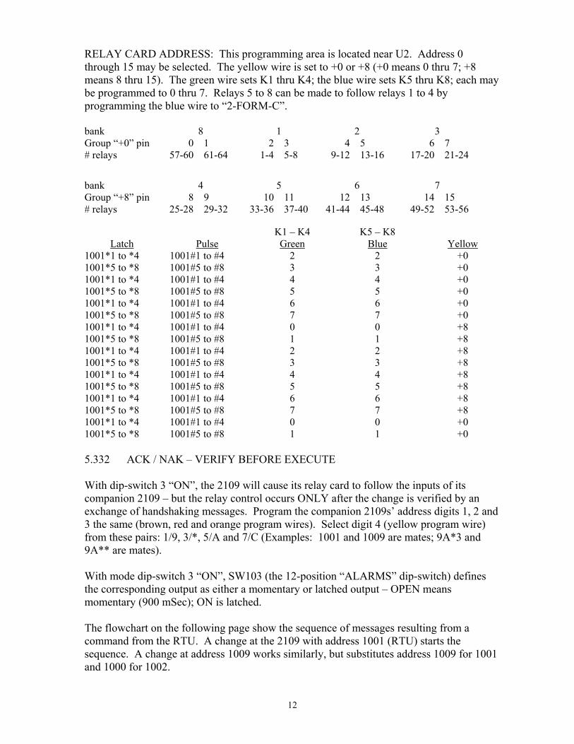
RELAY CARD ADDRESS: This programming area is located near U2. Address 0 through 15 may be selected. The yellow wire is set to +0 or +8 (+0 means 0 thru 7; +8 means 8 thru 15). The green wire sets K1 thru K4; the blue wire sets K5 thru K8; each may be programmed to 0 thru 7. Relays 5 to 8 can be made to follow relays 1 to 4 by programming the blue wire to “2-FORM-C”. bank 8 1 2 3 Group “+0” pin 0 1 2 3 4 5 6 7 # relays 57-60 61-64 1-4 5-8 9-12 13-16 17-20 21-24
bank 4 5 6 7 Group “+8” pin 8 9 10 11 12 13 14 15 # relays 25-28 29-32 33-36 37-40 41-44 45-48 49-52 53-56
K1 – K4 K5 – K8 Latch Pulse Green Blue Yellow
1001*1 to *4 1001#1 to #4 2 2 +0 1001*5 to *8 1001#5 to #8 3 3 +0 1001*1 to *4 1001#1 to #4 4 4 +0 1001*5 to *8 1001#5 to #8 5 5 +0 1001*1 to *4 1001#1 to #4 6 6 +0 1001*5 to *8 1001#5 to #8 7 7 +0 1001*1 to *4 1001#1 to #4 0 0 +8 1001*5 to *8 1001#5 to #8 1 1 +8 1001*1 to *4 1001#1 to #4 2 2 +8 1001*5 to *8 1001#5 to #8 3 3 +8 1001*1 to *4 1001#1 to #4 4 4 +8 1001*5 to *8 1001#5 to #8 5 5 +8 1001*1 to *4 1001#1 to #4 6 6 +8 1001*5 to *8 1001#5 to #8 7 7 +8 1001*1 to *4 1001#1 to #4 0 0 +0 1001*5 to *8 1001#5 to #8 1 1 +0 5.332 ACK / NAK – VERIFY BEFORE EXECUTE With dip-switch 3 “ON”, the 2109 will cause its relay card to follow the inputs of its companion 2109 – but the relay control occurs ONLY after the change is verified by an exchange of handshaking messages. Program the companion 2109s’ address digits 1, 2 and 3 the same (brown, red and orange program wires). Select digit 4 (yellow program wire) from these pairs: 1/9, 3/*, 5/A and 7/C (Examples: 1001 and 1009 are mates; 9A*3 and 9A** are mates). With mode dip-switch 3 “ON”, SW103 (the 12-position “ALARMS” dip-switch) defines the corresponding output as either a momentary or latched output – OPEN means momentary (900 mSec); ON is latched. The flowchart on the following page show the sequence of messages resulting from a command from the RTU. A change at the 2109 with address 1001 (RTU) starts the sequence. A change at address 1009 works similarly, but substitutes address 1009 for 1001 and 1000 for 1002.
12

1001 sends 1001sssaaa#. Digits 5, 6 and 7 (sss) represent the statuses of each of the 12 inputs. Digits 8, 9 and 10 (aaa) represent a momentary or latched function for each of the 12 inputs, defined by SW103. 1009: If it hears its mates 1001sssaaa#, it stores sss and echoes 1001sssaaa#. 1001: If the transmitted and echoed messages are equal, 1001 sends 1002sssaaa#. 1009: If it hears its mates execute command: 1002sssaaa#, it compares the input to the stored statuses. If they are equal, it controls the output relays; then echoes 1002sssaaa# to 1001. 1001: When it hears 1002sssaaa#, it clears relay 16. If the delivered message contains no “alarm” bits, and all inputs are in normal status, the optical isolator inputs are read and considered “old data.” EXCEPTIONS: If 1001 does not receive an echoed message for a time determined by the blue program wire, it repeats the original message 1001sssaaa#. If 1001 has sent the number of times indicated by the green program wire, it will indicate communication failure, by setting relay 16 (4th relay in the relay group programmed with yellow on +0 and green or blue on 5), but continue trying to deliver the message. If the echoed message is NOT equal to the transmitted message, 1001 re-sends the original 1001sssaaa# -- as if it had heard no response. If 1009 receives the execute command, but the received statuses are not equal to the stored statuses, 1009 returns the original message 1001sssaaa#. 5.333 AUTOANSWER / AUTODIAL Dip-switch 4 arms AutoAnswer / AutoDial operation – AND the ability to read from and write to the EEPROM via DTMF signaling. The AutoAnswer / AutoDial functions are controlled by dip-switches 4, 5 and 6. The AutoAnswer / AutoDial parameters (number of rings, answer seize time, telephone number, OFF-hook time, ON-hook time, etc.) are stored in the nonvolatile memory (EEPROM) installed in 2109 units (part number B02932-0100X) shipped after October 30, 1986. Dip-switch 5 determines whether answering the phone is adequate to satisfy the dialer’s requirement to deliver the message. If dip-switch 5 is OPEN, answering the phone satisfies the dialer; if it is ON, the 2109 will continue trying to deliver the message until it receives a DTMF 5. With dip-switch 5 ON, when the 2109 has been trying to deliver a message and is ON-hook between tries when it answers the phone, it will deliver its present status (and co-located analog encoder) readings, but it must receive a DTMF 5 to “unload its ‘stack’ of any old un-delivered messages” and stop re-dialing. Dip-switch 6 allows a choice between DTMF and pulse (rotary) dialing. 13
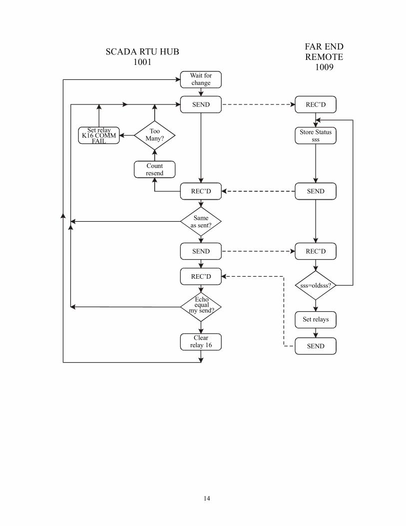
Wait forchange
SEND
TooMany?
Set relayK16 COMM
FAIL
Countresend
REC’D
Sameas sent?
SEND
REC’D
Echoequal
my send?
Clearrelay 16
REC’D
Store Statussss
SEND
REC’D
sss=oldsss?
Set relays
SEND
SCADA RTU HUB1001
FAR ENDREMOTE
1009
14

To send Verify-before-execute data (ACK/NAK) over PSTN lines, turn both dip-switch 3 and 4 ON, and follow both 5.332 and 5.333 instructions. 5.334 LONG DURATION STATUS CHANGES Dip-switch 7 arms a 2 minute delay routine for inputs 9-12. Brief changes might occur normally, whereas, sustained changes indicate a problem. Power failure indicators often false due to noise. To prevent a long distance telephone call to report a 3 second power failure, program dip-switch 7 “ON” and connect the power sensor to input 9, 10, 11 or 12. 5.4 EEPROM MEMORY SETTING – IS REMOTELY SET AutoAnswer/AutoDial: Dip-switch 4 arms AutoAnswer/AutoDial operation – AND the ability to read from and write into the EEPROM via DTMF signaling. The EEPROM contains 64 digits of information, grouped into 16 four digit registers. Each of the 64 digits is a character selected from the 16 DTMF characters. The 16 registers also correspond to the 16 DTMF characters. Registers 5, 6, 7, 8, A, B, C and D are reserved for future enhancements. Each of the registers is set via a six digit DTMF signal: r*abcd stores abcd into register r. For example, 1*2345 stores 2345 in register 1. To interrogate a register, dial r#. 1# should return DTMF 2345. Even if DDDD is stored in a register, the 2109 WILL return a DTMF message (revision F). Register Function Digit 1 Digit 2 Digit 3 Digit 4
1 Phone Number 1 2 3 4 2 5 6 7 8 3 9 10 11 12 4 13 14 15 16 9 Slave address 1 2 3 4 0 AutoAnswer Rings Answer 5 Seizetime Hold timer * AutoDial Dialpause OFFhook Onhook *
Registers 1 through 4 represent a “16 digit” telephone number, which will be dialed (if dip-switch 4 is “ON”) when the 2109 detects a change. Any of the 16 characters on the Model 2106 Base Master can be entered, but avoid , #, A, B and C. “DDDD” indicates an “empty” register, and causes the dialer to bypass it. The first non-empty register must begin with “D”, which represents a dial pause. The duration of the pause is programmable in register “” from 1 to 16 seconds. Do not end a telephone number with a D; arrange the number so that “digit filling D’s” occur before the last digit. To program the 2109 to call 9, 1, 513, 898-3621, send 1*d9d1, 2*d513, 3*d898, 4*3621. Registers 5, 6, 7 and 8 are reserved for a second telephone number to be implemented as a future expansion of the 2109 capabilities. Use register 9 to add a co-located slave encoder for additional data. Register 9 contains the four digit slave encoder address, which is interrogated after it has unloaded its ‘stack.’ After the interrogation, the 2109 is “deaf” for 10 seconds. If “DDDD” is in register 9, the 2109 skips this function. 15

Register 0 contains the AutoAnswer parameters: Digit 1 sets the number of rings the 2109 must receive before it answers the phone. The
sequence is the “Standard DTMF Sequence”: 1 thru 9 mean what you would expect, 0 means 10, * 11, # 12, A 13, B 14, C 15, D 16.
Digit 2 sets the AutoAnswer DTMF 5 duration, following the same sequence from 0.3 to 5
seconds (1 means 0.3, 16 means 5). Only functions when mode dipswitches 2 and 4 are ON – dialed ACK/NAK.
Digit 3 sets the AutoAnswer seize time equal to 0.5*N = 0.3 minutes (1 means 0.8 minutes;
D means 8.3 minutes). Digit 4 is the seize time due to receiving an interrogating DTMF 5. This timer is restored
with each DTMF 5. The timer is equal to 0.5*N = 0.3 minutes. Register * contains the AutoDial parameters: Digit 1 sets the duration of the pause (from 1 to 16 seconds) due to a “D” in a telephone
number. Digit 2 sets the OFF-hook time: the time (from 0.5 to 8 minutes) the 2109 will wait for a
DTMF 5 before giving up the try; equal to 0.5*N minutes. Digit 3 sets the ON-hook time: the time (from 0.5 to 8 minutes) the 2109 will wait ON-
hook between tries; also equal to 0.5*N minutes. Digit 4 is not used; use any number in this digit. Registers 5, 6, 7, 8, A, B, C and D are reserved for future enhancements. Signalcrafters Tech ships the 2109 with DDDD stored in all 16 registers, which sets the following default parameters AutoDial number defaults (registers 1-4): No (AutoDial) telephone number is installed. Slave address default (register 9): No Encoder will be interrogated. AutoAnswer defaults (register 0): The 2109 will AutoAnswer after 16 rings and keep the
line seized for 8.3 minutes. If the 2109 receives a DTMF “5”, it will keep the line seized for 8.3 minutes after the 5. If in PSTN/ACK/NAK mode (dip-switches 3 and 4 ON), upon AutoAnswer, the 2109 will transmit DTMF “5” for 5 seconds.
AutoDial time defaults (register *): The Dial-pause is 8 seconds. AutoDialing is at 8
minute OFF-hook and ON-hook times. If the 2109 is not installed in a Signalcrafters Tech pre-wired product, refer to page 6 for hookup instructions. The 2109 will hang up when it hears its four digit address followed by “DDD.” 16

5.5 ALIGNMENT 5.51 The alignment procedure outlined below should be performed before placing the 2109 into continuous service. Be sure all installer connections have been verified (see Installer Connections page 5) and all program wires are strapped properly (see paragraph 5.2). 5.52 The following test equipment is required for 2109 alignment procedures:
1. Oscilloscope with 1 MegOhm or higher input impedance. 2. Digital multimeter with 10 MegOhm or higher input impedance.
5.53 TRANSMIT LEVEL ADJUSTMENT – The front panel LEVEL potentiometer (R25) adjusts the transmit output level. A continuous DTMF character can be generated by holding the front panel SEND button depressed. 5.54 When setting output level, avoid setting it excessively high. If higher levels than necessary are used, distortion may be introduced into the signaling path, resulting in poor system performance. A radio microphone input may need to be less than 50 millivolts to avoid distortion. Levels used in telephone applications are usually from –16 dBm to 0 dBm. If it doesn’t work, try tuning it DOWN. The tone output may be measured across card-edge fingers 1 and 2, or 1 and 50. 5.55 Avoid over-deviation in radio transmitter applications. To set the proper level, press the send button and adjust the deviation to less than two-thirds of maximum – for most systems, the deviation should not exceed 2 KHz. 5.56 See paragraph 5.25 for TRANSMIT DELAY and 5.27 for REPEAT SEND INTERVAL programming information. These adjustments are by program wire settings. 6. TESTING 6.1 The following test equipment is required to perform the test procedures outlined below:
1. Oscilloscope with 1 MegOhm or higher input impedance. 2. Digital multimeter with 10 MegOhm or higher input impedance. 3. Signalcrafters Model 2106 or 2107 Base Master.
NOTE: All voltage readings are referenced to + common (card-edge finger 17). 6.2 The drawing on page 19 illustrates the appropriate connections for bench testing. Apply the appropriate power source (12, 24 or 48 VDC depending on the power supply option specified). 6.3 POWER SUPPLY – Measure the –5 VDC regulated power supply by connecting the probe of the digital multimeter to U102 pin 1 on the top board. Reading must be –5.00 ± 0.2 volts. On 24 and 48 VDC models, check the –12 VDC regulated supply by measuring the voltage present at U108 pin 3 on the top board. Reading must be –12.0 ± 0.5 VDC.
17

18
MAT
ERIA
L:
FIN
ISH
:
HEA
T TR
EAT:
BY
DAT
ED
ESC
RIPT
ION
REV
NEX
T AS
S’Y
FIR
ST U
SED
FINA
L A
SS’Y
FIR
EST
USE
D
B. D
. Num
ber
DR
AFTS
MAN
DATE
DATE
DAT
EC
HEC
KER
DES
IGN
DAT
E:EN
GIN
EER
TITL
E:EC
N N
O
SCA
LE:
CO
DE
IDEN
T.D
RW
G N
O:
DR
WG
NO
:
REV
REV
SHEE
T
OF
THIS
DR
AWIN
G A
ND IN
FORM
ATIO
N T
HER
EON
IS T
HE
PRO
PER
TY O
F SI
GN
ALC
RAFT
ERS
TEC
H A
ND A
LL
UNA
UTH
OR
IZED
USE
& R
EPR
OD
UCT
ION
IS P
ROH
IBIT
ED.
CAL
CA
L
UN
LESS
OTH
ERW
ISE
SPEC
IFIE
DA
LL D
IMEN
TIO
NS
IN,
I
NC
HES,
MET
RIC
(mm
):
m
m/IN
CHES
M
ETR
IC
DEC
IMA
LX.
XX.
XXAN
GLE
S,0.3
mm
0.13
mm
.XX
.XXX
.010
IN
.005
IN
INTE
RFA
CE
BO
AR
D
U8
U10
U11
U12
GR
EEN
T3
BLK
T2K
1
PRO
CES
SOR
BO
AR
D
U10
1U
102
U10
3
OPE
NSW
101
1 2
3 4
5 6
7 8
1 2 3 4 5 6 7 8 9101112
1 2 3 4 5 6 7 8 9101112
I N P U T S T A T E
A L A R M S
N.O
.
N.C
.O
NO
N
SW10
2SW
103
YEL
LOW
OR
GG
RN
BLU
EBR
NRED
GR
AY
VIO
LET
ALA
RM
/STA
TUS
ENC
OD
ER C
AR
D
B02
932-
XX
00X
B02
932-
XX
00X
5 52
4
5R
EDRA
WN
8184
0

CRYSTAL OSCILLATOR – Check the 3.58 MHz clock oscillator by connecting an oscilloscope to U105 pin 8 on the top board. The waveform should be a symmetrical square wave with a period of 0.28 uS. 6.4 ENCODER OPERATION – Connect the oscilloscope to U6 pin 10 on the lower board. Hold the front panel SEND button depressed. A sustained DTMF character should be generated. A 4 volt peak-to-peak DTMF waveform should be observed. Next, connect the oscilloscope to U6, pin 7. The amplitude will depend on the front panel LEVEL setting (potentiometer R25). Vary R25 from minimum to maximum. The peak-to-peak amplitude should vary from 0 to 4 volts. 6.5 DECODER OPERATION – Connect a DTMF source to the DTMF decoder input, card-edge fingers 55 and 56. Connect the oscilloscope to U2 pin 15, the DTMF decoder chip. Pin 15 will go high when any of the sixteen DTMF characters are received. Send DTMF characters and observe this point switching from low to high as the DTMF characters are received. 6.61 If U2 pin 15 does NOT go high during the presence of DTMF, connect the scope probe to the primary of transformer T1 (blue lead) and scope ground to card-edge finger 55. DTMF should be observed at this point when received. 6.62 If DTMF tones are present, connect the scope ground to card-edge finger 17 and the scope probe to the outputs of band split filter U1. Pin 2 is low group output and pin 11 is high group output. These low and high tone components are amplified by op-amps U3a pin 1 and U3c pin 14. 6.63 U4a and U4b are comparators used as Schmitt triggers, which provide 5 volt square waves into detector U2. U2’s output is one hexadecimal digit at U2 pins 5, 6, 7 and 8, corresponding to the input DTMF. The correlation table is shown in paragraph 10.63. 6.6 MULTIPLEXER OPERATION – PIA (Peripheral Interface Adapter) U102 on the top board reads several input lines which are selected by decade counter U111. Connect the oscilloscope probe to U111 pin 3. A square wave with a duty cycle of approximately 3 milliseconds should be observed. This is the selection of the 12 opto-coupler status inputs. A similar waveform should be seen at U111 pins 2, 4 and 7. 6.7 WATCHDOG TIMER – Connect the scope probe to U106 pin 11. Pulses will be seen at varying rates depending upon the mode of operation. These are generated within the program and constantly restart the timer. If pulses cease for more than one second, the watchdog will generate a 10 millisecond reset pulse at U101 pin 6 on the top board. 7. SPECIFICATIONS 7.1 GENERAL Controls and Indicators: 12 LEDs indicating presence of input current flow, 1 transmit LED, send button, transmit level adjustment. Encoder and Decoder Address: simultaneously set with four program wires; each address wire can be set to any of the 16 DTMF characters. 19

20
MAT
ERIA
L:
FIN
ISH
:
HEA
T TR
EAT:
BY
DAT
ED
ESC
RIPT
ION
REV
NEX
T AS
S’Y
FIR
ST U
SED
FINA
L A
SS’Y
FIR
EST
USE
D
B. D
. Num
ber
DR
AFTS
MAN
DATE
DATE
DAT
EC
HEC
KER
DES
IGN
DAT
E:EN
GIN
EER
TITL
E:EC
N N
O
SCA
LE:
CO
DE
IDEN
T.D
RW
G N
O:
DR
WG
NO
:
REV
REV
SHEE
T
OF
THIS
DR
AWIN
G A
ND IN
FORM
ATIO
N T
HER
EON
IS T
HE
PRO
PER
TY O
F SI
GN
ALC
RAFT
ERS
TEC
H A
ND A
LL
UNA
UTH
OR
IZED
USE
& R
EPR
OD
UCT
ION
IS P
ROH
IBIT
ED.
CAL
CA
L
UN
LESS
OTH
ERW
ISE
SPEC
IFIE
DA
LL D
IMEN
TIO
NS
IN,
I
NC
HES,
MET
RIC
(mm
):
m
m/IN
CHES
M
ETR
IC
DEC
IMA
LX.
XX.
XXAN
GLE
S,0.3
mm
0.13
mm
.XX
.XXX
.010
IN
.005
IN
EE-P
RO
M P
RO
GR
AM
MIN
GSE
TUP
CIR
CU
IT
MO
DEL
21
09ST
ATU
S EN
CO
DER
D I
P S
W I
T C
H
4 O
N
+ D
C C
OM
MO
N
-12
/ -24
/ -4
8 V
DC
OPT
O IN
PUT
1
DEC
OD
ER IN
PUT
ENC
OD
ER O
UTP
UT
56 55 17 40 39 * 2 1
DEC
OD
ER IN
PUT
ENC
OD
ER O
UTP
UT
GREEN
BLUE
GREEN/WHITE
BLUE/WHITE
1213
24
J3
MO
DEL
210
6 / 2
107
MA
STER
UN
IT
* P
IN 4
3 F
OR
12V
DC
SU
PPLY
P
IN 3
5 F
OR
24/
48V
DC
SU
PPLY
5R
EDRA
WN
8184
0
ALA
RM/S
TATU
S EN
COD
ER C
ARD
B02
932-
XX
00X
B02
932-
XX
00X
55
34

Supply Voltage: 12VDC--11 to 16.5VDC; 24VDC–21 to 28VDC; 48VDC–42 to 56VDC Current Drain: 75 milliamps maximum. Operating Temperature Range: -30 to +70 degrees Celsius. Dimensions: Height, 5.58” (14.2cM); Width, 1.42” (3.6cM); Depth, 5.53” (14.0cM). Weight: 17 ounces (480 grams). 7.2 ENCODER Input Capacity: 12 optically-isolated inputs Input Configuration: Optically isolated current sensors, capable of monitoring input currents of contacts; see application circuits on page 8. Opto-coupler Input Voltage Range: Same as power supply voltage. Current Limit resistor: 12 VDC—4.7 KOhms; 24 VDC–10 KOhms; 48 VDC–22 KOhms. Signaling Type: DTMF 2 of 8. Signaling Format: 11 digit DTMF burst (4 digits of address, 3 digits status, 3 digits alarm, and # for end of message). Signaling Speed: 40 mS. Tones with 40 mS. Interval between characters. Output Impedance: selectable to 600 or 900 Ohms – steered by relay contacts. Signal Level: Adjustable from –30 dBm to +3 dBm RMS into 600 Ohms. Tone Twist: 0.2 dB maximum (low to high tone imbalance) Multiple Send: Field set for Number of Sends from 1 to 9. Multiple Send Interval: Wire programmed from 5 to 60 Sec. In 5 Sec. Increments. Transmit Delay: 100, 200, 400 or 800 milliseconds, wire selectable. Input Recognition Delay: 100, 200, 400 or 800 milliseconds. Transmitter Keying: 2 form-C relay contacts rated 2 Amperes at 30 VDC or 0.6 Amperes at 125 VAC. Input Stack: 7 level buffer stores sequential opto input changes and outputs “stacked” information at 4 second intervals. Integral Report Timer: Automatically initiates a status update report. Programmable from master for a 1 to 99 hour interval (in 1 hour increments). 7.3 DECODER Signaling Type: DTMF 2 of 8. Input Impedance: 40 KOhms minimum, transformer-isolated and DC blocked. Input Level: 20 mV to 2.5 Vrms per tone. Sinad: Operates in the presence of noise with 16 dB sinad. Tone Twist Tolerance: 15 dB low to high tone imbalance. Signaling Speed: 40 milliseconds minimum tone ON time; 40 milliseconds minimum tone OFF time; Dip-switch 1 sets maximum OFF time. 21

Interdigit Timing (maximum OFF time): Field-programmable for “automatic” (100 milliseconds) or “manual” (2.5 seconds). 8. OPTIONS 8.1 Options for the 2109 are defined in the five digit suffix shown on the product part number label. The first two digits of the suffix relate to the installed EPROM which defines the “personality” of the card. The last suffix digit indicates the input power requirements. See below: Model 2109 Status Encoder Part Number – Suffix B02932 – X X 0 X X | 1 12 VDC | | | | 2 24 VDC | | | | 4 48 VDC | | | | | | | | 0 1.0” Standard Handle | | 1 0.5” Special Handle | | | | | 01 – 09 Standard Programs | | 10 – 99 Customer Application Specials 8.2 The input power requirement must be specified on each order. It is not readily changed in the field. The EPROM is socketed to allow field upgrades. 9. WARRANTY 9.1 Signalcrafters equipment described in this manual is warranted for a period of one year from date of shipment. Signalcrafters will repair or replace any unit which fails during this period due to defective material or workmanship. Unless specifically authorized, all in-warranty repairs will be made at the factory. Unauthorized field modification of the equipment will void the warranty. 10 CIRCUIT DESCRIPTION This section provides circuit description for both the Interface and the Processor board assemblies. NOTE: All voltage readings are referenced to + common card-edge finger 17). 10.1 PROCESSOR CARD (circuit D17926-00001) 10.2 MICROPROCESSOR/PIAs/EPROM – U101 is an 8 bit CMOS processor (MPU) which interfaces to all inputs and outputs via Ics U102 and U103. These are Peripheral Interface Adapters (PIAs) with two 8-bit ports and 4 control lines. The program for the 2109 is contained in U104, an Erasable Programmable Read Only Memory (EPROM). 22

10.21 The 12 opto-couplers, the program wires, and the dip-switches are multiplexed via a decade counter, U111, which selects what is to be read. The counter’s clock and reset lines are controlled by 2 outputs from PIA U102. 10.22 When U222 is reset, it selects the 12 opto-couplers. Removing the reset and pulsing the clock line once will cause U111 to select the DTMF decoder and dip-switch SW101. Pulse 2 selects the 12 position INPUT STATE dip-switch, SW102; U112 and U114 are tri-state buffers which function as ‘diodes’ which pull lines to + common if a switch is closed. Pulse 3 selects an identical circuit to read the ALARM dip-switch SW103. 10.23 Pulses 4 to 7 select site address wires A1 to A4. Pulse 8 selects both the NO. OF SENDS and TX DELAY program wires. Pulse 9 selects both REPEAT SEND INTERVAL and RECOGNITION TIME program wires. 10.24 Relays K1 and K2 are controlled by U103, PB10, CA12 and CB12. U105c and U109 decode the MPU selection of the relay coil to be energized. 10.25 U105a is the 3.58 MHz crystal clock oscillator, which is buffered by U105b. U105d provides a chip select for EPROM U104. 10.26 Output tones originate in the microprocessor as a timed sequence of 8 bit words communicated to U108, via PIA U103, PA10-PA17. U108 produces a current into U6a, proportional to the value of its input data. 10.3 POWER-ON RESET CIRCUIT – This circuit provides a hardware reset for microprocessor U101, when power is applied to the unit. U107 generates this reset pulse due to R104 and C103, giving a 250 milliseconds reset pulse. This circuit causes a reset pulse if the 5 VDC supply should fall below 4.5 VDC. 10.4 WATCHDOG TIMER – This circuit will provide an automatic hardware reset to the microprocessor in the event that U106 does not receive repeated timer restarts. In normal operation, pulses are generated by the microprocessor and appear at U103 pin 10. These pulses (re-) trigger timer U106b. As long as these pulses are received, the U106 pin 7 remains high. If pulses cease for more than one second, pin 7 will pulse low for 10 milliseconds, pulling U107 pin 3 low, restarting the microprocessor. 10.5 INTERFACE CARD (circuit D17925-00001) 10.51 The 12 alarm/status inputs are applied to 3 quad opto-couplers (U10-U12). Resistors R38-R41 provide current limiting. The 12 front panel LEDs are in series with these inputs, and therefore indicate the presence of input current. The 12 opto-coupler outputs are routed to the top board to U102. Diodes CR18-CR29 prevent damage due to polarity reversal. 10.53 The C.O.R. input is applied via R23 and U7 to PIA U103. If the NO/NC program wire is connected to the ‘N.O.’ pin, the data is inverted by Q1. 10.54 The front panel TRANSMIT LED is controlled by PIA U103, PB11. It lights when Transmit Relay K1 is energized, and pulses off during tones. 23

10.55 Relay K1 is controlled by driver transistors Q101 and Q102 on the processor card. It is magnetic latching, controlled by a 5 millisecond pulse to either the set or reset coils. K1 has 2 form-C contacts. K1-1 contacts are used for transmitter keying or PSTN line seize. K1-2 contacts may be used to mute “other” audios during the encoder tones. 10.56 K2 is controlled by driver transistors Q103 and Q104. Both form-C contacts of this control relay are brought out to the card-edge fingers. The relay control is either latched or momentary, via DTMF. 10.6 DTMF DECODER – Incoming DTMF at card-edge fingers 55 and 56 is coupled to transformer T1 via C1, R48 and C16. This transformer configuration provides an isolated, 40 KOhm input impedance. The secondary is fed to bandsplit filter U1 through resistor R1. Diodes CR1 and CR2 provide transient protection. The 3.58 MHz clock signal from the processor card is applied to U1 pin 15. U1 pin 14 replicates this clock to U2 pin 2. 10.61 Bandsplit filter U1 is a switched-capacitor filter which separates the DTMF low tone and high tones. The low tone at U1 pin 2 is amplified by U3a and U4a, and applied to decoder chip U2 pin13. Similarly, the high tone from U1 pin 11 is amplified by U3c and U4b and fed to U2 pin 4. 10.62 Op amp U3b serves as a buffer for the high impedance reference voltage at U1 pin 5. The buffered –2.5 VDC on U3b pin 7 serves as a reference voltage for Ics U3 and U4. 10.63 Decoder chip U2 provides a hexadecimal output on pins 5, 6, 7 and 8 for each of the DTMF characters. Pin 15 is a “character presence” line, which goes high when a valid DTMF character is detected. Pin 9 is an input (tri-state output enable) which enables the hexadecimal output. All these pins are routed to a PIA on the processor card. The output of U2 is a hexadecimal representation of the DTMF input as follows:
DTMF CHARACTER IN U2 PIN NUMBER HEX CHARACTER 8 7 6 5
1 0 0 0 1 1 2 0 0 1 0 2 3 0 0 1 1 3 4 0 1 0 0 4 5 0 1 0 1 5 6 0 1 1 0 6 7 0 1 1 1 7 8 1 0 0 0 8 9 1 0 0 1 9 0 1 0 1 0 A * 1 0 1 1 B # 1 1 0 0 C A 1 1 0 1 D B 1 1 1 0 E C 1 1 1 1 F D 0 0 0 0 0
10.7 ENCODER FILTER AND AMPLIFIER – The synthesized tones from U108 is fed to U6a. This amplifier drives a low pass filter (C9-C11, R18-19 and T3). The output of the filter is applied to U6c, a voltage follower. The follower in turn drives push-pull 24

amplifier U6a and U6b. Potentiometer R25 is the front panel LEVEL control. The outputs of U6a and U6b drive transformer T2 through the 600/900 Ohm impedance selector jumper. The secondary of T2 is routed to the connector via the TX Relay steering contacts (K102). 10.8 POWER SUPPLY – U8, a negative voltage regulator, provides –5 VDC, used internally as a relative common. The + DC input (0) is the positive supply; the –12 VDC (input or regulator U9 output used in the 24 and 48 VDC versions of the 2109) is the negative supply. Diode CR51 protects from transients. On the 48 VDC version, CR52 is in series with the negative supply input. 10.9 EXPANSION – PB13, PB15 and PB16 pins from PIA U103 on the processor card are brought to the connector. These are for communications with companion products, including Models 2450, 2451 and 2452 relay cards. 11. PARTS LIST 11.1 The following components are located on the interface (bottom) board assembly C17981-0000X. Tighter tolerance components as well as higher voltage capacitors and higher wattage resistors may be substituted for the parts in this list – provided that they are small enough to fit. If not specified, ±5% ¼ watt resistors, and ±10% 20VDC capacitors may be used as replacement parts. Component Semiconductors:
Description Part Number Quantity
Q1, 2 2N5306 A11622-00001 2 CR1, 2, 34 1N4148 A11514-00001 3 CR3, 4, 18-33 1N4004 A10279-00001 19 CR5-17 LED, right angle mount A17944-00001 13 CR35-49 Not Used CR50 Power Supply Option Dependent => 12 VDC Not Used => 24/48 VDC 1N4004 A10279-00001 1 CR51 Power Supply Option Dependent => 12 VDC 1N6278A Suppressor A17354-A0200 1 => 24/48 VDC 1N6284A Suppressor A17354-A0360 1 CR52 Power Supply Option Dependent => 12/24 VDC Not Used => 48 VDC 1N5359A Regulator B17762-A0240 1 U1 8865 DTMF Filter A14739-08865 1 U2 8860 DTMF Decoder A14739-08860 1 U3, 6 3403 Quad Op Amp A14814-03403 1 U4 3302 Quad Comparator A14814-03302 1 U5, 7 TIL111 Optical Coupler A14333-00002 2 U8 7905 -5 Volt Regulator A14902-07905 1 U9 Power Supply Option Dependent => 12 VDC Not Used => 24/48 VDC 7912 -12 Volt Regulator A14903-07912 1 U10, 11, 12 Quad Optical Coupler A15943-00001 3 U13 X2444 NOVRAM A17966-02444 1 25

Component Non-Semiconductors:
Description Part Number Quantity
R1, 21 10 KOhm A16923-10004 2 R2, 28, 30, 31 1 KOhm A16923-10003 4 R3, 4 120 KOhm A16923-12005 2 R5, 6 1.5 MegOhm A16923-15006 2 R7, 8 47 KOhm A16923-47004 2 R9, 10, 48 15 KOhm A16923-14004 3 R11, 12 1 MegOhm A16923-10006 2 R13-14, 18, 22, 44, 45, 46 100 KOhm A16923-10005 7 R15 330 KOhm A16923-33005 1 R16 220 KOhm A16923-22005 1 R17, 23 Power Supply Option Dependent => 12 VDC 3.3 KOhm A16923-33003 2 => 24 VDC 6.8 KOhm A16923-68003 2 => 48 VDC 13 KOhm A16923-13004 2 R19 11.3 KOhm ±1% 1/8 watt A13112-11304 1 R20 1.5 KOhm A16923-15003 1 R24 47.5 KOhm ±1% 1/8 watt A13112-47504 1 R25 50 KOhm Potentiometer A13371-50004 1 R26, 27, 43 Not Used R33, 34, 37 10 KOhm ±1% 1/8 watt A13112-10004 3 R35 97.6 Ohm ±1% 1/8 watt A13112-97601 1 R36 127 Ohm ±1% 1/8 watt A13112-12702 1 R42 33 KOhm A16923-33004 1 R47 10 Ohm A16923-10001 1 R49-60 Power Supply Option Dependent => 12 VDC 4.7 KOhm A16923-47003 12 => 24 VDC 10 KOhm A16923-10004 12 => 48 VDC 22 KOhm A16923-22004 12 C1 .1 uF Mylar B13093-10410 1 C2, 15 .01 Uf Ceramic A00256-00100 2 C3, 4 .001 uF Ceramic A12108-10210 2 C5, 6 33 pF Ceramic A12108-33010 2 C7, 8 .33 uF Mylar B13093-33310 2 C9, 17 1 uF 35V Tant B13006-10535 2 C10 1800 pF ±3% Poly B13635-18203 1 C11 220 pF ±3% Poly B13635-22103 1 C12 4300 pF ±3% Poly B13635-43203 1 C13 100 uF 25V Aluminum B16787-10735 1 C14 33 uF 16V Tant B13006-33616 1 C16 .0047 uF Mylar B13093-47210 1 C18 Power Supply Option Dependent => 12 VDC Not Used => 24/48 VDC 33 uF 16V Tant B13006-33616 1 SW1 Not Used SW2 Push-Button Send Switch A17945-00001 1 J1A Inter-board Connector A17559-10028 1 J1B Inter-board Connector A17559-10008 1
26
Component Non-Semiconductors:
Description Part Number Quantity
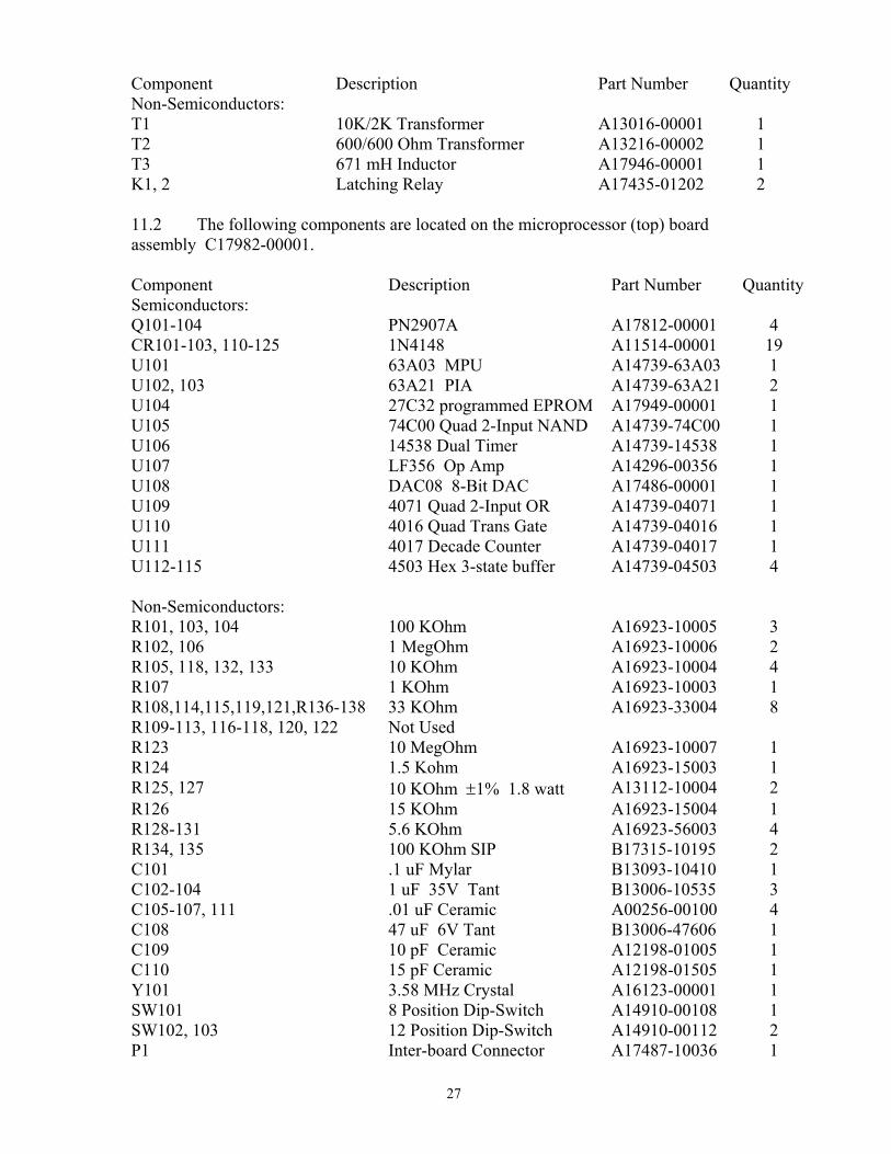
T1 10K/2K Transformer A13016-00001 1 T2 600/600 Ohm Transformer A13216-00002 1 T3 671 mH Inductor A17946-00001 1 K1, 2 Latching Relay A17435-01202 2 11.2 The following components are located on the microprocessor (top) board assembly C17982-00001. Component Semiconductors:
Description Part Number Quantity
Q101-104 PN2907A A17812-00001 4 CR101-103, 110-125 1N4148 A11514-00001 19 U101 63A03 MPU A14739-63A03 1 U102, 103 63A21 PIA A14739-63A21 2 U104 27C32 programmed EPROM A17949-00001 1 U105 74C00 Quad 2-Input NAND A14739-74C00 1 U106 14538 Dual Timer A14739-14538 1 U107 LF356 Op Amp A14296-00356 1 U108 DAC08 8-Bit DAC A17486-00001 1 U109 4071 Quad 2-Input OR A14739-04071 1 U110 4016 Quad Trans Gate A14739-04016 1 U111 4017 Decade Counter A14739-04017 1 U112-115 4503 Hex 3-state buffer A14739-04503 4 Non-Semiconductors: R101, 103, 104 100 KOhm A16923-10005 3 R102, 106 1 MegOhm A16923-10006 2 R105, 118, 132, 133 10 KOhm A16923-10004 4 R107 1 KOhm A16923-10003 1 R108,114,115,119,121,R136-138 33 KOhm A16923-33004 8 R109-113, 116-118, 120, 122 Not Used R123 10 MegOhm A16923-10007 1 R124 1.5 Kohm A16923-15003 1 R125, 127 10 KOhm ±1% 1.8 watt A13112-10004 2 R126 15 KOhm A16923-15004 1 R128-131 5.6 KOhm A16923-56003 4 R134, 135 100 KOhm SIP B17315-10195 2 C101 .1 uF Mylar B13093-10410 1 C102-104 1 uF 35V Tant B13006-10535 3 C105-107, 111 .01 uF Ceramic A00256-00100 4 C108 47 uF 6V Tant B13006-47606 1 C109 10 pF Ceramic A12198-01005 1 C110 15 pF Ceramic A12198-01505 1 Y101 3.58 MHz Crystal A16123-00001 1 SW101 8 Position Dip-Switch A14910-00108 1 SW102, 103 12 Position Dip-Switch A14910-00112 2 P1 Inter-board Connector A17487-10036 1 27