model 372xxa vector network analyzer maintenance … · 2016-03-18 · the 372xxa series vector...
TRANSCRIPT
490 JARVIS DRIVE MORGAN HILL, CA 95037-2809
MODEL372XXA
VECTOR NETWORK ANALYZER
MAINTENANCE MANUAL
P/N: 10410-00153REVISION: B
PRINTED: JULY 1996COPYRIGHT 1995 WILTRON CO.

WARRANTYThe WILTRON product(s) listed on the title page is (are) warranted against defects in materialsand workmanship for one year from the date of shipment.WILTRON’s obligation covers repairing or replacing products which prove to be defective duringthe warranty period. Buyers shall prepay transportation charges for equipment returned to WIL-TRON for warranty repairs. Obligation is limited to the original purchaser. WILTRON is not liablefor consequential damages.
LIMITATION OF WARRANTYThe foregoing warranty does not apply to WILTRON connectors that have failed due to normalwear. Also, the warranty does not apply to defects resulting from improper or inadequate mainte-nance by the Buyer, unauthorized modification or misuse, or operation outside of the environmentalspecifications of the product. No other warranty is expressed or implied, and the remedies providedherein are the Buyer’s sole and exclusive remedies.
TRADEMARK ACKNOWLEDGEMENTSV Connector and K Connector are registered trademarks of WILTRON Company.ANACAT is a registered trademark of EEsof, Inc.Ink Jet and Think Jet are registered trademarks of Hewlett-Packard Co.MS-DOS is a registered trademark of Microsoft Corporation.
NOTICEWILTRON Company has prepared this manual for use by WILTRON Company personnel andcustomers as a guide for the proper installation, operation and maintenance of WILTRON Companyequipment and computer programs. The drawings, specifications, and information contained hereinare the property of WILTRON Company, and any unauthorized use or disclosure of these drawings,specifications, and information is prohibited; they shall not be reproduced, copied, or used in wholeor in part as the basis for manufacture or sale of the equipment or software programs without theprior written consent of WILTRON Company.

Table of Contents
Chapter 1 — General Service InformationThis chapter provides a general description of Series 37200A Vector Network Analyzer systems,system serial numbers, and frequency ranges. It explains the level of maintenance covered in thismanual and the service strategy used throughout this manual. It also contains static-sensitive com-ponent handling precautions and a list of recommended test equipment.
Chapter 2 — Replaceable PartsThis chapter lists all replaceable subassemblies and components for all 372XXA models. It explainsthe WILTRON exchange assembly program and provides parts ordering information.
Chapter 3 — Operational TestsThis chapter contains procedures that provide a means of fully testing the 372XXA VNA system forproper operation and signal stability. These tests are intended to be used as a periodic check of theoperational functionality of the 372XXA.
Chapter 4 — Performance Verification ProceduresThis chapter provides detailed procedures for verifying that the performance of the 372XXA meetsminimum performance standards.
Chapter 5 — TroubleshootingThis chapter provides information for troubleshooting Series 37200A Vector Network Analyzer sys-tems. The troubleshooting procedures contained in this chapter support fault isolation down to areplaceable subassembly.
Chapter 6 — AdjustmentsThis chapter provides adjustment procedures for all models of Series 37200A Vector Network Ana-lyzer systems. These procedures are used after replacement or repair of one or more critical subas-semblies, or as indicated by the Performance Verification Procedures contained in Chapter 4.
Chapter 7 — System DescriptionThis chapter provides descriptions of the functional operation of the major assemblies contained inSeries 37200A Vector Network Analyzer systems. The operation of all major circuit blocks is de-scribed so that the reader may better understand the function of each assembly as part of the overalloperation.
Chapter 8— Removal and Replacement ProceduresThis chapter describes how to gain access to all of the major assemblies and major parts fortroubleshooting and/or replacement.
Appendix A — Diagnostic MenusThis appendix contains descriptions and usage information for the Diagnostic Menus that are avail-able via the front panel Option Menu key.
Appendix B — Error Codes/MessagesThis appendix contains a listing of the Error Codes/Messages. Also included is a description of theinformation fields that are part of the error messages.
372XXA MM i

Appendix C — Connector Maintenance Check ProceduresThis appendix contains procedures and information needed to perform maintenance checks (includingpin-depth measurements) for the connectors on all WILTRON supplied Calibration/Verification Kitcomponents, Through-cables, and other associated RF/microwave components.
Appendix D — Performance SpecificationsThis appendix contains performance specifications for all models in the 372XXA Series Vector Net-work Analyzer.
Appendix E — Verification Software Users GuideThis appendix contains the Model 360X/372XXA VNA Performance Verification Software UsersGuide, P/N: 10410-00162. This Software Users Guide explains in detail the procedures to be used forthe installation and operation of the 372XXA VNA Verification Software on your computer/controller.
Index
Table of Contents — Continued
ii 372XXA MM

Table of Contents
1-1 SCOPE OF MANUAL . . . . . . . . . . . . . . . . 1-5
1-2 INTRODUCTION . . . . . . . . . . . . . . . . . . 1-5
1-3 IDENTIFICATION NUMBER . . . . . . . . . . . . 1-5
1-4 SYSTEM DESCRIPTION . . . . . . . . . . . . . . 1-5
1-5 RELATED MANUALS . . . . . . . . . . . . . . . . 1-6
1-6 STANDARD OPTIONS . . . . . . . . . . . . . . . 1-6
1-7 SERVICE STRATEGY . . . . . . . . . . . . . . . . 1-6
Functional Assembly Level Troubleshooting . . . . . . . . . . . . . . . . . 1-7
Internal Hardware Adjustments and Calibrations . . . . . . . . . . . . . . . . . . . 1-7
Internal Service Log . . . . . . . . . . . . . . 1-7
System Test/ Certification . . . . . . . . . . . . . . . . . . . 1-8
Preventive Service . . . . . . . . . . . . . . . . 1-8
Servicing Specially Modified Instruments . . . 1-8
Chapter 1 General Information

1-8 SERVICE SUPPORT INFORMATION . . . . . . . 1-8
Technical Support . . . . . . . . . . . . . . . . 1-8
Field Service Kits . . . . . . . . . . . . . . . . 1-9
Service Software . . . . . . . . . . . . . . . . . 1-9
Verification Kits . . . . . . . . . . . . . . . . . 1-10
Test Fixtures/ Aids . . . . . . . . . . . . . . . . 1-10
Failed Assembly Exchange Program . . . . . . 1-10
1-9 RECOMMENDED TEST EQUIPMENT . . . . . . 1-10
1-10 STATIC SENSITIVE COMPONENT HANDLING PROCEDURES . . . . . . . . . . . . 1-12
1-11 SERVICE CENTERS . . . . . . . . . . . . . . . . 1-12
1-12 PERFORMANCE SPECIFICATIONS . . . . . . . 1-12

Figure 1-1. Series 37200A Vector Network Analyzer System
1-4 372XXA MM

1-1 SCOPE OF MANUAL This manual provides general service and preventive maintenance in-formation for the WILTRON 372XXA family of Vector Network Ana-lyzer (VNA) systems. It contains procedures for:
Testing the instrument for proper operation.
Verifying measurement accuracy and traceability to National In-stitute of Standards and Technology (NIST).
Troubleshooting a failed instrument to the exchange subassemblylevel or the subsystem requiring adjustment.
Adjusting instrument internal sub-systems.
Locating and replacing failed parts.
Throughout this manual, the terms “372XXA” and “372XXA VNA” willbe used interchangeably to refer to all Series 37200A Network Ana-lyzer system models, unless otherwise noted.
1-2 INTRODUCTION This chapter of the manual provides a general description of 372XXAVNA systems, system serial numbers, frequency ranges, and relatedmanuals. Also included is information about the level of maintenance cov-ered in this manual, service strategy, available service facilities, and static-sensitive component handling precautions. A list of recommended testequipment is also provided.
1-3 IDENTIFICATION NUMBER All WILTRON instruments are assigned a six-digit ID number, such as“401001”. This number appears on a decal affixed to the rear panel. Pleaseuse this identification number during any correspondence with WILTRONCustomer Service about this instrument.
1-4 SYSTEM DESCRIPTION The 372XXA Analyzers are microprocessor controlled Vector Network Ana-lyzers. Each is a single-instrument system that contains a built-in signalsource, a test set, and an analyzer subsystem. A typical model (37269A)is shown in Figure 1-1 (facing page). These analyzers are produced infive models that cover a range of from 22.5 MHz to 40 GHz. The tableat left lists the frequencies for each model.
Chapter 1General Information
Model Freq Range
32711A 22.5 MHz to 3.0 GHz
37217A 22.5 MHz to 8.6 GHz
37225A 40.0 MHz to 13.5 GHz
37247A 40.0 MHz to 20.0 GHz
37269A 40.0 MHz to 40.0 GHz
372XXA Model Frequencies
372XXA MM 1-5

1-5 RELATED MANUALS The 372XXA Vector Network Analyzer Operation Manual (10410-00149)describes the front panel operation for all 372XXA models. It also containsgeneral information, specifications, and Performance Verification proce-dures for all models.
The 372XXA Series Vector Network Analyzer Programming Manual(10410-00160) describes all 372XXA GPIB commands and providesprogramming information for operation of the 372XXA remotely via theIEEE-488 General Purpose Interface Bus. Included at the rear of thismanual is the 372XXA Series Vector Network Analyzer GPIB QuickReference Guide (10410-00164).
Model 360X/372XXA VNA Performance Verification Software UsersGuide, P/N: 10410-00162 (located in Appendix E at the rear of thismanual). This Software Users Guide explains in detail the proceduresto be used for the installation and operation of the 372XXA VNA Verifi-cation Software on your computer/controller.
1-6 STANDARD OPTIONS The standard 372XXA VNA options and their respective Upgrade Kit partnumbers are:
1-7 SERVICE STRATEGY This paragraph provides an overview of the 372XXA VNA service strategyand available service facilities. It also provides references to theinformation in various locations in this manual needed to accomplish theservice functions required for the 372XXA VNA.
Appendices - Refer to the Appendices at the rear of this manual for de-tailed descriptions of the following:
Diagnostics Menus and GPIB Commands.
Error Messages.
System Block Diagrams.
Parts Locator Diagrams.
Option* Description Upgrade Kit
Opt 1 Rack Mount ND39486
Opt 2 Time Domain ND39477
Opt 3 1 Hz Frequency Resolution(Standard for 37217A and 37211A)
ND39478
Opt 6 Port 2 Test Attenuator ND39480
Opt 10 High Stability Ovenized Time Base ND39481
Opt 11 Rear Panel Reference LoopExtension Cables
ND39482
∗ All options listed can be installed at WILTRON Service Centers
GENERAL SERVICE INFORMATION STRATEGY
1-6 372XXA MM

Functional AssemblyLevel
Troubleshooting
The 372XXA modular design, extensive built-in diagnostics, and auto-mated service tools are designed to support fast exchange of functional as-sembly level repairs.
Failed assemblies are not field repairable. Once an assembly is foundto be faulty, it should be returned to an authorized WILTRON ServiceCenter for exchange. Refer to the description of the Exchange Assem-bly Program in Chapter 2, Replaceable Parts.
The procedures for troubleshooting a failed 372XXA VNA are describedin this manual in Chapter 5, Troubleshooting.
Internal HardwareAdjustments and
Calibrations
There are two automated internal hardware field calibrations which areused to characterize the 372XXA frequency and power generation sub-sys-tems. These calibrations insure fast, consistent phase lock of system fre-quencies and proper compensation, leveling, and flatness of system powerat the front panel test ports.
To conduct these calibrations, you need only connect the appropriatetest equipment (counter or power meter) to the 372XXA and initiatethe calibration. The 372XXA will control itself and the externally con-nected test equipment to perform measurements and store calibrationconstants in its internal battery backed RAM (BBRAM).
The procedures for adjusting the 372XXA VNA are described in thismanual in Chapter 6, Adjustments.
Internal Service Log The 372XXA continuously monitors itself for proper operation. Should afailure occur, it notifies the user via a failure message on the displayscreen. (In remote-only operation, it also sets the GPIB Status Byte, if en-abled.) It also writes the error message along with some data pertinent tothe failure to an internal service log stored in battery backed memory.
The service log can be checked at any time to view (without erasing) allerror messages that were written into it. It is capable of storing morethan 30 pages of service messages and data. The 372XXA will automat-ically remove the oldest errors first to make room for new errors, if nec-essary. To check the contents of the service log, use the proceduredescribed in Chapter 3, Operational Tests.
NOTEA printed or disk file copy of the Service Log (with the fail-ure in question) must be made available to WILTRONwhen exchanging a failed assembly, or when requestingservice support. Refer to Chapter 2, Replaceable Parts, forfurther information.
SERVICE GENERAL STRATEGY INFORMATION
372XXA MM 1-7

System Test/ Certification
Quick operational checkout of the system may be accomplished by the sys-tem user or for incoming inspection purposes using the “OperationalCheckout” chapter in the 372XXA Operations Manual. Those proceduresare useful in quickly verifying that the instrument’s primary measure-ment functions are operational and stable.
Full operational testing of the system is detailed in Chapter 3, Opera-tional Tests. These tests should be performed annually, or more oftendepending on system use.
Verification of the system’s measurement accuracy and other key per-formance parameters may be done using the procedures in Chapter 4,Performance Verification. This should be performed annually, or moreoften depending on system use.
Preventive Service The 372XXA A9 Processor PCB contains a battery backed memory/realtime clock chip (BBRAM) and a static memory (SRAM) backup battery.These have a finite life span and should be replaced periodically per theprocedures in Chapter 8, Removal and Replacement Procedures.
The BBRAM chip has a rated life span of 4 years. The SRAM backupbattery has a worst case elapsed time for SRAM battery protection of200 days. The SRAM battery life span will vary according to how thesystem is used; that is, how often the system is powered off for ex-tended periods of time.
Servicing SpeciallyModified Instruments
Instruments with customer requested special modifications performed byWILTRON will have an identifying Specials Modification number printedon the rear panel. This number will be preceded with the letters SM, i.e.,SM1234 is special modification number 1234.
Special instruments may have service requirements different fromthose specified in this manual. Contact your local Service Center if youneed more information when servicing such instruments.
1-8 SERVICE SUPPORTINFORMATION
The following paragraphs briefly describe the various service support serv-ices and aids available to you to help you maintain your 372XXA.
Technical Support Technical service support is available by contacting any WILTRON World-wide Service Center (refer to paragraph 1-11). Or, service support may beobtained directly from the factory by contacting:
WILTRON Company ATTN: Customer Service 490 Jarvis Drive Morgan Hill, CA 95037-2809
Telephone: (408)-778-2000FAX: (408)-778-0239
GENERAL SERVICE SUPPORTINFORMATION INFORMATION
1-8 372XXA MM

If servicing or repairing your own system and you need technical sup-port, you will need to FAX or mail a printout of the items listed belowto the WILTRON Customer Support Engineer:
Measurement data in question“Operational Tests” resultsSystem state (from UTILITY menu)Service Log (from DIAGNOSTICS menu)
Field Service Kits The field service kits listed below are available through your local WIL-TRON Sales or Service Center:
ND37200A-1, Field Exchange Assembly KitThis kit contains all field exchangeable assemblies in the 372XXA (seethe Parts Chapter for the exchange assembly list). The kit is packagedin two hardened rolling cases plus a separate box for the CRT.
ND37200A-11, Performance Verification KitThis kit provides for automated field test and performance verificationof the 372XXA. It is packaged in a hardened rolling case that also hasspace for two, user supplied, verification and calibration kits and otheraccessories.
The ND37200A-11, Performance Verification Kit is comprised of the fol-lowing:
Service Software The service software listed below is contained on the diskette located atthe rear of this manual:
Wiltron 37200A Test Software (2300-178).This software contains a series of automated tests designed to insurethe 372XXA signal paths are functioning properly and capable of sup-porting stable calibrations and measurements. See Operational TestsChapter for details.
Wiltron 37200A Performance Verification Software (2300-175).This software is used to verify the 372XXA published measurement ac-curacy and traceability to the U.S. National Institute of Standards andTechnology (NIST). See Chapter 4, Performance Verification, for details.
SERVICE SUPPORT GENERAL INFORMATION INFORMATION
360CC-3 Note-book Computer (w/ battery and power adapter)
RS-232/GPIB-US
Serial Port to GPIB Adapter with 2 Meter GPIB Cable.The -UK or -EU shipped for United Kingdom or Europeas appropriate. All other locations use -US
2300-175 37200A Verification Software
2300-178 37200A Test Software
B39553 Printer Test Connector
2100-2 GPIB cable
372XXA MM 1-9

Verification Kits The WILTRON Verification Kits listed below are used in conjunction withthe 37200A Performance Verification Software (above). See Chapter 4, Per-formance Verification, for further information.
GPC-7 Verification Kit (Model 3667)Contains precision GPC-7 Connector components whith characteristicsthat are traceable to the NIST. Use for Models 37217A and below.
K Verification Kit (Model 3668)Contains precision K Connector components that are traceable to theNIST. Use for Models 37225A and above.
Test Fixtures/ Aids The test fixtures and test aids listed below are available through your lo-cal WILTRON Sales or Service Center:
Rear Panel Printer Port Test Fixture (B39553).This test fixture is used to check out digital printer interface circuits onthe rear panel assembly.
GPIB Cable (2100-2).This cable is used to check out digital GPIB interface circuits on therear panel assembly.
Failed AssemblyExchange Program
The exchange program allows a customer to quickly exchange a failed sub-assembly for a factory refurbished, fully system-tested and unit that is un-der warranty. This results in significant time and price savings ascompared with ordering a new assembly.
Refer to Chapter 2, Replaceable Parts, for a complete list of exchange-able assemblies for all Series 37200A models.
NOTEWhen sending a failed assembly to the factory for ex-change, a copy of the Service Log must always accompanythe failed assembly. Refer to Chapter 2, Replaceable Parts,for further information.
1-9 RECOMMENDED TESTEQUIPMENT
Table 1-1 lists the recommended test equipment to be used for all mainte-nance activities for all Series 37200A models. Note the “Use” codeslisted in the right hand column of the table. These codes list the applica-ble maintenance activities for the equipment listed.
GENERAL RECOMMENDEDINFORMATION TEST EQUIPMENT
1-10 372XXA MM

INSTRUMENTCRITICAL
SPECIFICATIONRECOMMENDED
MANUFACTURER/MODELUSE**
Computer/Controller Equipped with National InstrumentsGPIB Interface Adapter, w/DriverSoftware V2.1 or later
WILTRON 360CC or 360CC-2, with a PCII/IIA, or, WILTRON 360CC-3and RS-232/GPIB-US (or -UK/ -EU)
O, P
37200A Test Software WILTRON 2300-178 O
Floppy Disk Formatted, IBM PC format DS/HD 1.44 Mbyte A
GPIB Cable WILTRON 2100-2, or equivalent O, P, A
RF/Microwave Cable DC – 40 GHz, K type connectors (male or female), Length, 3 ft.
Any P, A
BNC Cable Length, 4 ft., 2 each Any O
Printer Port Test Fixture
WILTRON B39553 O
Thru Line For models 37217A and below:For models 37225A and above:
WILTRON 3670A50-2, 3671A50-2WILTRON 3670K50-2, 3671K50-2
O, P
Calibration Kit For models 37217A and below:For models 37225A and above:
WILTRON 3651-1*WILTRON 3652-1*
O, P
37200A PerformanceVerification Software
WILTRON 2300-175 P
Connector VerificationKit
For models 37217A and below:For models 37225A and above:
WILTRON 3667WILTRON 3668
P
Assurance Air Line For models 37217A and below:For models 37225A and above:
WILTRON 18A50WILTRON T1519
P
Offset Termination For models 37217A and below:For models 37225A and above:
WILTRON 29A50-20WILTRON 29KF50-15
P
Frequency Counter Frequency: 0.1 to 26.5 GHzInput Impedance: 50Ω
EIP Microwave, Inc., Model 578B P, A
Digital Multimeter Resolution: 41⁄2 digits DC Accuracy: 0.1 % AC Accuracy: 0.1 %
Any T
Oscilloscope Bandwidth: DC to 100 MHzSensitivity: 2 mVHoriz. Sensitivity: 50 ns/division
Tektronix, Inc.Model 2445
T
∗ Calibration Kit sliding load (Option -1), required for Performance Verification only.
∗∗ USE CODES:A Adjustment / Internal Hardware CalibrationO Operational TestingP Performance VerificationT Troubleshooting
Table 1-1. Recommended Test Equipment (1 of 2)
RECOMMENDED TEST GENERAL EQUIPMENT INFORMATION
372XXA MM 1-11

1-10 STATIC SENSITIVECOMPONENTHANDLINGPROCEDURES
The 372XXA contains components that can be damaged by static electric-ity. Figure 1-2 (opposite page) illustrates the precautions that should be fol-lowed when handling static-sensitive subassemblies and components. Iffollowed, these precautions will minimize the possibilities of static-shockdamage to these items.
1-11 SERVICE CENTERS WILTRON Company offers a full range of repair and calibration servicesat fully staffed and equipped service centers throughout the world. Table 2-1, located on page 2-4, lists all WILTRON services centers.
1-12 PERFORMANCESPECIFICATIONS
The performance specifications for all Series 372XXA models are con-tained in the Technical Data Sheets that are located in Appendix D, Per-formance Specifications.
GENERAL SERVICE INFORMATION CENTERS
INSTRUMENTCRITICAL
SPECIFICATIONRECOMMENDED
MANUFACTURER/MODELUSE**
Power Meter 1, with: Power Range: –30 to +20 dBm (1 mW to 100 mW)Other: GPIB controllable
HP 437B with Option 22 (GPIB) P, A
Power Sensor 1 or:
Power Meter 2, with:Power Sensor 2
Frequency Range: 0.05 to 50 GHzPower Range: –70 to +47 dBm (100 pW to 50 W)Other: GPIB controllableFrequency Range: 0.01 to 40 GHz
HP 8487A
Gigatronics 8541 or 8542Gigatronics 80304A
P, A
Gauging Set GPC-7 Gauging SetK Connector Gauging Set
WILTRON 01-161WILTRON 01-162
O, T
∗∗ USE CODES:A Adjustment / Internal Hardware CalibrationO Operational TestingP Performance VerificationT Troubleshooting
Table 1-1. Recommended Test Equipment (2 of 2)
1-12 372XXA MM

1. Do not touch exposed contacts onany static sensitive component.
2. Do not slide static sensitivecomponent across any surface.
3. Do not handle static sensitivecomponents in areas where the flooror work surface covering is capable ofgenerating a static charge.
4. Wear a static-discharge wristbandwhen working with static sensitivecomponents.
5. Label all static sensitive devices. 6. Keep component leads shortedtogether whenever possible.
7. Handle PCBs only by their edges. Donot handle by the edge connectors.
8. Lift & handle solid state devices bytheir bodies – never by their leads.
9. Transport and store PCBs and otherstatic sensitive devices in static-shielded containers.
10. ADDITIONAL PRECAUTIONS:
• Keep workspaces clean and free of any objects capable of holding or storing a static charge.
• Connect soldering tools to an earth ground.
• Use only special anti-static suction or wick-type desoldering tools.
Figure 1-2. Static Sensitive Component Handling Procedures
COMPONENT HANDLING GENERAL PROCEDURES INFORMATION
372XXA MM 1-13

Table of Contents
2-1 INTRODUCTION . . . . . . . . . . . . . . . . . . 2-3
2-2 EXCHANGE ASSEMBLY PROGRAM . . . . . . . 2-3
2-3 REPLACEABLE SUBASSEMBLIES AND PARTS 2-3
2-4 PARTS ORDERING INFORMATION . . . . . . . . 2-4
Chapter 2Replaceable Parts

Chapter 2Replaceable Parts
2-1 INTRODUCTION This chapter provides replaceable parts information for all 372XXAmodels. The major replaceable 372XXA assemblies and parts are listedin Tables 2-2 through 2-7. The locations of these assemblies/parts areshown in Figures 2-1 through 2-3.
2-2 EXCHANGE ASSEMBLYPROGRAM
WILTRON maintains a module exchange program for selected subassem-blies. If a malfunction occurs in one of these subassemblies, the defectiveitem can be exchanged. Upon receiving your request, WILTRON will shipthe exchange subassembly to you, typically within 24 hours. You thenhave 45 days in which to return the defective item. All exchange subas-semblies or RF assemblies are warranted for 90 days from the date ofshipment, or for the balance of the original equipment warranty, which-ever is longer.
NOTEWhen sending a failed assembly to the factory for ex-change, a copy of the Service Log must always accom-pany the failed assembly. This copy may be a printout,or a saved disk copy. Due to the importance of the serv-ice log information to the WILTRON factory Service En-gineers, the exchange prices are only valid if theservice log data is included with the failed assembly.
Please have the exact model number and serial number of your unitavailable when requesting this service, as the information about yourunit is filed according to the instrument’s model and serial number. Formore information about the program, contact your local sales repre-sentative or call WILTRON Customer Service direct (refer to para-graph 2-4.
2-3 REPLACEABLESUBASSEMBLIES ANDPARTS
Tables 2-2 through 2-5, (starting page 2-5) list the major replaceablesubassemblies and parts for the 372XXA. These assemblies/parts are pres-ently covered by the WILTRON exchange assembly program. Table 2-6(page 2-6) lists disposable parts for the 372XXA, and Table 2-7 lists fac-tory-repairable parts for the 372XXA. (The parts listed in Tables 2-6 and2-7 are not presently on the exchange assembly program.)
NOTEThe 372XXA A17 Motherboard PCB Assembly is not afield-replaceable item.
372XXA MM 2-3

2-4 PARTS ORDERINGINFORMATION
All parts listed in Tables 2-2 through 2- 7 may be ordered from your localWILTRON service center (Table 2-1). Or, they may be ordered directlyfrom the factory at the following address:
WILTRON Company ATTN: Customer Service 490 Jarvis Drive Morgan Hill, CA 95037-2809
Telephone: (408)-778-2000FAX: (408)-778-0239
UNITED STATESWILTRON COMPANY490 Jarvis DriveMorgan Hill, CA 95037-2809Telephone: (408) 778-2000FAX: (408) 778-0239
ANRITSU WILTRON COMPANY685 Jarvis DriveMorgan Hill, CA 95037-2809Telephone: (408) 776-8300FAX: (408) 776-1744
ANRITSU WILTRON COMPANY10 Kingsbridge RoadFairfield, NJ 07004Telephone: (201) 227-8999FAX: (201) 575-0092
AUSTRALIAWILTRON PTY. LTD.Level 2, 410 Church StreetNorth ParramattaNSW 2151 AustraliaTelephone: 026-30-81-66Fax: 026-83-68-84
BRAZILANRITSU WILTRON ELECTRONICALTDA.Praia de Botafogo, 440-SL 2401-Botafogo2225-Rio de Janeiro-RJ-BrasilTelephone: 021-28-69-141Fax: 021-53-71-456
CANADAANRITSU WILTRON INSTRUMENTS LTD.215 Stafford Road, Unit 102Nepean, Ontario K2H 9C1Telephone: (613) 828-4090FAX: (613) 828-5400
CHINAWILTRON BEIJING SERVICECENTER
416W Beijing Fortune Building5 Dong San Huan Bei LuChao Yang Qu, Beijing 100004, ChinaTelephone: 86-1-50-17-559FAX: 86-1-50-17-558
FRANCEANRITSU WILTRON S.A9 Avenue du QuebecZone de Courtaboeuf91951 Les Ulis CedexTelephone: 016-44-66-546FAX: 016-44-61-065
GERMANYANRITSU WILTRON GmbHRudolf Diesel Strabe 178031 GilchingTelephone: 08-10-58-055FAX: 08-10-51-700
INDIAMEERA AGENCIES (P) LTD.A-23 Hauz KhasNew Delhi 110 016Telephone: 011-685-3959FAX: 011-686-6720
ISRAELTECH-CENT, LTDHaarad St. No. 7, Ramat HaahayalTel-Aviv 69701Telephone: (03) 64-78-563FAX: (03) 64-78-334
ITALYANRITSU WILTRON Sp.ARoma OfficeVia E. Vittorini, 12900144 Roma EURTelephone: (06) 50-22-666FAX: (06) 50-22-4252
JAPANANRITSU CORPORATION
1800 Onna Atsugi-shiKanagawa-Prf. 243 JapanTelephone: 0462-23-1111FAX: 0462-25-8379
KOREAWILTRON CORPORATION#2103 Korea World Trade Center159-1 Samsung-DongKangnam-ku, SeoulTelephone: (02) 551-2250FAX: (02) 551-4941
SINGAPOREANRITSU WILTRON (SINGAPORE) PTELTD3 Shenton Way #24-03Shenton HouseSingapore 0106Telephone: 011-65-2265206FAX: 011-65-2265207
SWEDENANRITSU WILTRON ABBox 247S-127 25 SkarholmenTelephone: (08) 74-05-840FAX: (08) 71-09-960
TAIWANWILTRON CO., LTD.8F, No. 96, Section 3Chien Kuo N. RoadTaipei, Taiwan, R.O.C.Telephone: (02) 515-6050FAX: (02) 509-5519
UNITED KINGDOMANRITSU WILTRON LTD.200 Capability GreenLuton, BedfordshireLU1 3LU, EnglandTelephone: 05-82-41-88-53FAX: 05-82-31-303
Table 2-1. WILTRON Service Centers
REPLACEABLE PARTS ORDERINGPARTS INFORMATION
2-4 372XXA MM

ReferenceDesignator
372XXAOption
Assembly / Part Part Number
A1 LO1 D40949-3
A2 LO2 D38502-3
A3 Test A IF D38503-4
A4 Reference IF D38504-3
A5 A/D D38505-3
A6 Test B IF D38503-5
A7 LO3 D38507-3
A7 Opt 10 LO3 D38507-4
A8 Source Lock/ Separation Control D38508-3
A9 Main Processor B38509
A13 I/O #1 D38513-3
A14 I/O #2 D38514-3
A15 Graphics Processor D38515-3
A16 Hard Disk (w/ PCB) D41041-3
A18 Rear Panel PCB D38518-3
A19** Front Panel Switch PCB P/O ND39473
A20** Front Panel Control PCB P/O ND39473
A21A1 Source YIG/Bias Control (p/o Signal Source Module) D38521-3
A21A2 Source Control (p/o Signal Source Module) D38522-3
A24 VME Bus Terminator D38524-3
∗ These PCB assemblies are used for all models of WILTRON Series 37200A VNA systems. ∗∗ These PCB’s are part of the Front Panel Assembly (refer to Table 2-5).
Table 2-2. Printed Circuit Board Assemblies*
Assembly / Part 372XXA Model / Option Part Number
Transfer Switch All D27030-2
Step Attenuator, 70 dB All 4612K
Low Frequency Bridge w/ Bias Tee 37211A, 37217A D28066
Coupler w/ Bias Tee 37225A and higher D28477-1
Power Amplifier All D25035-1
20 GHz Quad Buffer Amp/Sampler 37247A and below D25014
40 GHz Quad Buffer Amp/Sampler 37269A only D26815
Table 2-3. Test Set Assembly RF/Microwave Components (1 of 2)
PARTS REPLACEABLELISTS PARTS
372XXA MM 2-5

Assembly / Part 372XXA Model / Option Part Number
Level Detector Set Assembly All C24950-1
Switched Doubler Module (SDM) 37269A only D27075
Port 2 Step Attenuator Opt 6 only 4612K
6 dB Pad 37269A only 43KC-6
20 dB Pad 37247A and below 43KC-20
Table 2-3. Test Set Assembly RF/Microwave Components (2 of 2)
Assembly / Part 372XXA Model / Option Part Number
YIG Oscillator (2 - 20 GHz) All C21620-1
Down Converter All D27532
Switched Filter All D26805
Table 2-4. Signal Source Module RF/Microwave Components
Assembly / Part 372XXA Model / Option Part Number
10 MHz Ovenized Oscillator Opt 10 only ND39476
Power Supply Module All 40-55
VGA Monitor All 2000-322
Floppy Disk Assy All C38550
Front Panel Assy (w/ Front Panel, A19 and A20 PCB’s, and all Model ID Overlays)
All ND39473
Fan Assembly, Rear Panel All B38533
Table 2-5. Miscellaneous /Integrated Assemblies
Assembly / Part 372XXA Model / Option Part Number
System Software All B40918
Front Panel Encoder Knob All 2000-577
Front Panel Amber Lens All 790-412
Fuse, 8A, Fast Blow 3AG Cartridge type (F1 Line fuse for power supply assembly)
All 631-72
Table 2-6. Consummsable Parts
REPLACEABLE PARTSPARTS LISTS
2-6 372XXA MM

Front Panel Assembly(Includes Front Panel PCB)
VGA MonitorAssembly
SignalSourceModule
PowerSupplyModule
Ovenized Reference Oscillator(Option 10 only)
Printed Circuit BoardAssemblies, A1-A9
Fan Assembly
Printed CircuitBoard Assemblies,
A13-A16
Figure 2-1. 372XXA Major Assemblies Location Diagram (Top 3⁄4 View)
Assembly / Part 372XXA Model / Option Part Number
Test Port Connector, K-Male 37225A and higher 34UK50
Table 2-7. Factory Repairable Non-Exchange Parts
MAJOR ASSEMBLIES REPLACEABLELOCATION DIAGRAM PARTS
372XXA MM 2-7

Port 2Coupler/Bridge*
Floppy Disk DriveAssembly
Level DetectorAssemblies
A17 MotherboardPCB Assembly
A24 VME BusTerminator
PCB Assembly
Port 1Coupler/Bridge*
Step Attenuator70 dB
TransferSwitch
PowerAmplifier
6 dB/20 dB Pads*Refer to Table 2-3Model 37269A OnlyOption 6 Only
***
A18 Rear PanelPCB Assembly
20/40 GHzQuad Buffer
Amp/Sampler*
Switched DoublerModule**
Port 2 StepAttenuator#
#
Figure 2-2. 372XXA Major Assemblies Location Diagram (Bottom View)
REPLACEABLE MAJOR ASSEMBLIESPARTS LOCATION DIAGRAM
2-8 372XXA MM

Switched Filter
A21A2 SourceControl PCB
Down Converter
A21A1 Source YIGBias Control PCB
2-20 GHz YIGOscillator Assembly
Figure 2-3. Signal Source Parts Location Diagram
372XXA MM 2-9/2-10
MAJOR ASSEMBLIES REPLACEABLELOCATION DIAGRAM PARTS

Table of Contents
3-1 INTRODUCTION . . . . . . . . . . . . . . . . . . 3-3
3-2 CHECKING THE SERVICE LOG . . . . . . . . . 3-4
3-3 SELF TEST . . . . . . . . . . . . . . . . . . . . . . 3-5
3-4 PERIPHERALS AND INTERFACES TESTS . . . . 3-6
CRT Display Test . . . . . . . . . . . . . . . . 3-6
Front Panel Test . . . . . . . . . . . . . . . . . 3-7
External Keyboard Interface Test . . . . . . . 3-7
Printer Interface Test . . . . . . . . . . . . . . 3-7
GPIB Interface Test . . . . . . . . . . . . . . . 3-9
3-5 SIGNAL PATH TESTS . . . . . . . . . . . . . . . . 3-10
Chapter 3Operational Tests

Chapter 3Operational Tests
3-1 INTRODUCTION The tests in this section provide a means of fully testing the 372XXA VNAsystem for proper operation and signal stability. These tests are intendedto be used as a periodic check of the operational functionality of the372XXA.
The tests should be performed in their entirety at least once annually.Although there is no requirement to do so, the tests should generally berun in the sequence presented.
NOTEThe procedures presented in Chapter 4, Performance Verifi-cation, provide the means to test the accuracy of the testsperformed by the 372XXA.
Please ensure you have read and fully understand the servicing con-cepts for the 372XXA presented in Chapter 1 prior to continuing withthis chapter.
Operational Tests for the 372XXA consist of the following:
Checking the Service Log
Self Test
Peripherals and Interface Testing
Signal Path Tests (includes Checking the Service Log and SelfTest.)
These tests are described in paragraphs 3-2 through 3-5, which start onthe next page.
372XXA MM 3-3

3-2 CHECKING THE SERVICE LOG
Checking the service log consists of viewing the entries written into the log.
CAUTIONThe service log contains historical information about instru-ment condition and any failures that may have occurred. Itshould be cleared only by a qualified service engineer. Suchclearing shuld be accomplished only upon determining thatthe errors need not be saved to disk, or printed out for serv-ice purposes.
Procedure:
Step 1. Press the Option Menu key (Enhancement key group) todisplay the OPTIONS menu.
Step 2. Select DIAGNOSTICS from menu (left); then selectREAD SERVICE LOG from the DIAGNOSTICS menu.
The 372XXA will now display the contents of the servicelog. The display consists of a header and an error listing.The header contains a variety of system service informa-tion. The error listing contains error messages for failuresthat may have occurred during operation.
NOTE• Errors 7201–7209, GPIB remote operation
programming errors, report that one ormore external GPIB programming errorshas been detected. These messages do notindicate a 372XXA system fault.
• Informational messages 0000–0099 reportthe pass/fail status of a peripheral access.These messages do not indicate a 372XXAsystem fault.
Any other error messages in the service log may indicate aninstrument problem and should be investigated. Refer tothe Chapter 5, Troubleshooting, for further information.
CAUTION
The CLEAR SERVICE LOG menu selec-tion will immediately and permanently clearall the error message entries from the serv-ice log. (However, it will not clear the headerinformation.) See Caution message at top ofpage.
OPERATIONAL CHECKING THETESTS SERVICE LOG
OPTIONS
TRIGGERS
REAR PANEL OUTPUT
DIAGNOSTICS
MULTIPLE SOURCECONTROL
PRESS <ENTER>TO SELECT
DIAGNOSTICS
START SELF TEST
READ SERVICE LOG
INSTALLED OPTIONS
PERIPHERAL TESTS
TROUBLESHOOTING(FOR SERVICEONLY)
HW CALIBRATIONS(FOR SERVICEONLY)
PRESS <ENTER>TO SELECT
3-4 372XXA MM

3-3 SELF TEST The self test performs a series of tests that verify that various internal372XXA circuits are functional and operating properly.
To start the self test:
Step 1. Press the Option Menu key (Enhancement key group) todisplay the OPTIONS menu.
Step 2. Select DIAGNOSTICS from menu; then select STARTSELF TEST (below).
Step 3. Wait for test sequence to complete. (Once invoked, this testrequires no user interaction or external equipment.)
Upon completion, the net pass/fail result of the self test is shown on theCRT display. If the 372XXA is in remote-only operation, the results arereported via the GPIB output buffer. If the self test fails, detailed errormessages will be written into the service log.
If self test fails:
Check the service log to view failure messages.
Proceed to Chapter 5, Troubleshooting.
OPTIONS
TRIGGERS
REAR PANEL OUTPUT
DIAGNOSTICS
MULTIPLE SOURCECONTROL
PRESS <ENTER> TOSELECT
DIAGNOSTICS
START SELF TEST
READ SERVICE LOG
INSTALLED OPTIONS
PERIPHERAL TESTS
TROUBLESHOOTING(FOR SERVICEONLY)
HW CALIBRATIONS(FOR SERVICEONLY)
PRESS <ENTER> TOSELECT
SELF OPERATIONALTEST TESTS
372XXA MM 3-5

3-4 PERIPHERALS ANDINTERFACES TESTS
These tests are used to verify the operation of the CRT display, front panelkeys, and peripheral devices that are used with the 372XXA. They consistof the following:
CRT Display Test
Front Panel Test
External Keyboard Interface Test
Printer Interface Test
GPIB Interface Test
CRT Display Test This test verifies that the 372XXA CRT display is functioning correctly.
NOTEThe External VGA Out Connector can also be tested whenusing this procedure if an external VGA monitor is con-nected.
Procedure:
Step 1. Press the Option Menu key (Enhancement key group) todisplay the OPTIONS menu.
Step 2. Select DIAGNOSTICS from menu; then in sequence select:PERIPHERAL TESTS, and then CRT DISPLAY. See dia-gram below.
Step 3. Follow instructions on the CRT screen until test is com-pleted.
If test fails, proceed to Chapter 5, Troubleshooting.
OPTIONS
TRIGGERS
REAR PANEL OUTPUT
DIAGNOSTICS
MULTIPLE SOURCECONTROL
PRESS <ENTER> TOSELECT
DIAGNOSTICS
START SELF TEST
READ SERVICE LOG
INSTALLED OPTIONS
PERIPHERAL TESTS
TROUBLESHOOTING(FOR SERVICEONLY)
HW CALIBRATIONS(FOR SERVICEONLY)
PRESS <ENTER> TOSELECT
PERIPHERAL TESTS
CRT DISPLAY
FRONT PANEL
EXTERNAL KEYBOARD
PRINTER INTERFACE
GPIB INTERFACE
PREVIOUS MENU
PRESS <ENTER> TOSELECT
OPERATIONAL PERIPHERALS ANDTESTS INTERFACES TESTS
3-6 372XXA MM

Front Panel Test This test verifies that the control keys in each of the 372XXA key groupsare functioning correctly.
Procedure:
Step 1. Press the Option Menu key (Enhancement key group) todisplay the OPTIONS menu.
Step 2. Select DIAGNOSTICS from menu; then in sequence select:PERIPHERAL TESTS, and then FRONT PANEL. Seediagram below.
Step 3. Follow instructions on the screen until test is completed.
If test fails, proceed to Chapter 5, Troubleshooting.
External KeyboardInterface Test
This test verifies that the 372XXA external keyboard interface is function-ing correctly.
Equipment Required:
An IBM compatible keyboard is required for this test.
Procedure:
Step 1. Press the Option Menu key (Enhancement key group) to dis-play the OPTIONS menu.
Step 2. Select DIAGNOSTICS from menu; then in sequence select:PERIPHERAL TESTS, and then EXTERNAL KEY-BOARD. See diagram above.
Step 3. Follow instructions on the screen until test is completed.
If test fails, proceed to Chapter 5, Troubleshooting.
Printer Interface Test This test verifies that the 372XXA printer interface is functioning cor-rectly.
OPTIONS
TRIGGERS
REAR PANEL OUTPUT
DIAGNOSTICS
MULTIPLE SOURCECONTROL
PRESS <ENTER> TOSELECT
DIAGNOSTICS
START SELF TEST
READ SERVICE LOG
INSTALLED OPTIONS
PERIPHERAL TESTS
TROUBLESHOOTING(FOR SERVICEONLY)
HW CALIBRATIONS(FOR SERVICEONLY)
PRESS <ENTER> TOSELECT
PERIPHERAL TESTS
CRT DISPLAY
FRONT PANEL
EXTERNAL KEYBOARD
PRINTER INTERFACE
GPIB INTERFACE
PREVIOUS MENU
PRESS <ENTER> TOSELECT
PERIPHERALS AND OPERATIONALINTERFACES TESTS TESTS
372XXA MM 3-7
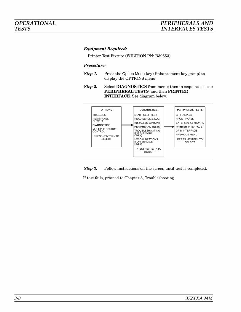
Equipment Required:
Printer Test Fixture (WILTRON PN: B39553)
Procedure:
Step 1. Press the Option Menu key (Enhancement key group) todisplay the OPTIONS menu.
Step 2. Select DIAGNOSTICS from menu; then in sequence select:PERIPHERAL TESTS, and then PRINTERINTERFACE. See diagram below.
Step 3. Follow instructions on the screen until test is completed.
If test fails, proceed to Chapter 5, Troubleshooting.
OPTIONS
TRIGGERS
REAR PANEL OUTPUT
DIAGNOSTICS
MULTIPLE SOURCECONTROL
PRESS <ENTER> TOSELECT
DIAGNOSTICS
START SELF TEST
READ SERVICE LOG
INSTALLED OPTIONS
PERIPHERAL TESTS
TROUBLESHOOTING(FOR SERVICEONLY)
HW CALIBRATIONS(FOR SERVICEONLY)
PRESS <ENTER> TOSELECT
PERIPHERAL TESTS
CRT DISPLAY
FRONT PANEL
EXTERNAL KEYBOARD
PRINTER INTERFACE
GPIB INTERFACE
PREVIOUS MENU
PRESS <ENTER> TOSELECT
OPERATIONAL PERIPHERALS ANDTESTS INTERFACES TESTS
3-8 372XXA MM

GPIB Interface Test This test verifies that the 372XXA printer interface is functioning cor-rectly.
Equipment Required:
GPIB cable (WILTRON PN: 2100-2), or equivalent
CAUTIONInsure that no other cables are connected to either of thetwo rear panel GPIB ports when performing this test.
Procedure:
Step 1. Press the Option Menu key (Enhancement key group) todisplay the OPTIONS menu.
Step 2. Select DIAGNOSTICS from menu; then in sequence select:PERIPHERAL TESTS, and then GPIB INTERFACE.See diagram below.
Step 3. Follow instructions on the screen until test is completed.
If test fails, proceed to Chapter 5, Troubleshooting.
OPTIONS
TRIGGERS
REAR PANEL OUTPUT
DIAGNOSTICS
MULTIPLE SOURCECONTROL
PRESS <ENTER> TOSELECT
DIAGNOSTICS
START SELF TEST
READ SERVICE LOG
INSTALLED OPTIONS
PERIPHERAL TESTS
TROUBLESHOOTING(FOR SERVICEONLY)
HW CALIBRATIONS(FOR SERVICEONLY)
PRESS <ENTER> TOSELECT
PERIPHERAL TESTS
CRT DISPLAY
FRONT PANEL
EXTERNAL KEYBOARD
PRINTER INTERFACE
GPIB INTERFACE
PREVIOUS MENU
PRESS <ENTER> TOSELECT
PERIPHERALS AND OPERATIONALINTERFACES TESTS TESTS
372XXA MM 3-9

3-5 SIGNAL PATH TESTS These are a series of automated tests designed to insure the 372XXA inter-nal signal paths are functioning properly and are capable of supportingstable calibrations and measurements. These test are performed using asoftware test program and an external computer/controller.
The test software performs the following operations and tests:
Service Log Check
Self Test
Basic Sweep Operation and Speed Test
High Level Noise Test
System Stability Test
RF Power Generation and Control Test
Step Attenuators Accuracy and Repeatability Test
Video IF Bandwidth Filters Operation Test
Sampler Efficiency and Stability Test
LO1/LO2 Linearity Test
Source FM/Lock Signal Linearity Test
Equipment required:
372XXA Test Software (WILTRON PN: 2300-178)
IBM Compatible PC with VGA Graphics Adapter and Mouse
External computer/controller; refer to Table 1-1 located on page 1-9.
GPIB cable (WILTRON PN: 2100-2), or equivalent
Procedure:
Step 1. Using the GPIB cable, connect the external computer/con-troller to the IEEE 488.2 GPIB Interface port on the 372XXArear panel.
Step 2. Install test software (WILTRON PN: 2300-178) to the harddrive. (Insert software disk in floppy drive and — depend-ing on whether 3.5-inch floppy is A: or B: — at the DOSprompt, type A:\INSTALLA or B:\INSTALLB.
Step 3. Change to directory 372ADIAG, and type 372atest at theDOS prompt. (Note: Program will not run from the floppydisk.)
Step 4. After entering operator name and instrument information,select Individual Tests. Then select Transmission Tests.
OPERATIONAL SIGNAL PATHTESTS TESTS
3-10 372XXA MM

Step 5. Follow the directions displayed on the computer screen toperform all tests.
If any tests fail, refer to the Troubleshooting and Help selections of theTest Software menu for assistance.
NOTETo exit the program, simultaneously press keys <Ctrl + C>or <Ctrl + Break>.
372XXA MM 3-11/3-12

Table of Contents
4-1 INTRODUCTION . . . . . . . . . . . . . . . . . . 4-3
4-2 CALIBRATION AND MEASUREMENT CONDITIONS . . . . . . . . . . . . . . . . . . . . 4-3
Standard Conditions . . . . . . . . . . . . . . 4-3
Special Precautions: . . . . . . . . . . . . . . . 4-4
4-3 VERIFYING MEASUREMENT ACCURACY . . . 4-4
Verification Software . . . . . . . . . . . . . . 4-4
Verification ResultDetermination . . . . . . . . . . . . . . . . . . 4-5
4-4 PERFORMANCE VERIFICATION PROCEDURE 4-5
4-5 MEASUREMENT OF KEY SYSTEM PERFORMANCE PARAMETERS . . . . . . . . . 4-6
Measurement Environment Considerations . . 4-6
MeasurementTechnique . . . . . . . . . . . . . . . . . . . . 4-7
Chapter 4Performance Verification

Chapter 4Performance Verification
4-1 INTRODUCTION This chapter provides specific procedures to be used to verify that the372XXA is making accurate, traceable S-parameter measurements. Youshould perform the verification procedures in paragraph 4-3, “VerifyingMeasurement Accuracy,” at least once annually.
Additionally, this chapter includes procedures that may be used tomeasure the following key system performance parameters:
Effective Source Match
Effective Directivity
System Dynamic Range
Frequency Accuracy
Power Level Accuracy
The Operational Tests described in Chapter 3 should be performedprior to verifying system performance.
Please ensure you have read and fully understand the servicing con-cepts for the 372XXA presented in Chapter 1 prior to continuing withthis chapter.
4-2 CALIBRATION ANDMEASUREMENTCONDITIONS
Extremes in the surrounding environmental conditions and the conditionand stability of the test port connectors, through-cable, and calibration kitdetermine system measurement integrity to a large extent.
These are all user controlled conditions, and as such, should be evalu-ated periodically for impact on system performance. If these conditionsvary significantly with time, the system verification procedures shouldbe performed more often than the recommended annual cycle.
Standard Conditions The standard conditions specified below must be observed when perform-ing any of the operations in this chapter — both during calibration andduring measurement.
Warm-up Time: One hour minimum.Environmental Conditions:
Temperature: 23 +/- 3 deg CRelative Humidity: 20-50% recommended.
372XXA MM 4-3

Error Correction:Full 12 Term sliding load calibration, including
isolation, 1024 averages, and 100 Hz Video IF BW setting.
Special Precautions: When performing the procedures in this chapter, observe the following pre-cautions:
Minimize vibration and movement of system and attached compo-nents and through-cable.Clean and check pin depth and condition of all adapters, through-cable(s), and calibration components.Pre-shape the through-cable(s) so as to minimize its movementduring calibration and measurement activities.Ensure the system remains motion free in stable environmentalconditions as defined above throughout warm-up, calibration, andmeasurement activities.
4-3 VERIFYINGMEASUREMENTACCURACY
The verification procedures described in the following paragraphs verifythe published measurement accuracy and measurement traceability* forthe 372XXA.
Verification Software These procedures use the WILTRON 37200A Verification Software, PN:2300-175, and the NIST traceable impedance transfer standards con-tained in the appropriate WILTRON Verification Kit. The Standard Condi-tions and Special Precautions described in paragraph 4-2 should beobserved when performing these procedures.
The appropriate WILTRON Verification Kit to be used for performingthese procedures is model dependent, as follows:
Models 37217A and below: Verification Kit 3667Models 37225A and above: Verification Kit 3668
The impedance transfer standards contained in these kits are:
20 dB Attenuation Standard50 dB Attenuation Standard50 Ohm Air Line Standard25 Ohm Mismatch (Beatty) Standard
The verification software performs the following functions:
It guides the user through a full 12 Term calibration of the372XXA.It guides the user through the measurement of the S-parametersof the NIST traceable impedance transfer standards (below).It verifies the measured values are within the specified measure-ment uncertainty limits.
∗ Traceability to the U.S. National Institute of Standards and Technology (NIST)
PERFORMANCE VERIFYINGVERIFICATION MEASUREMENT ACCURACY
4-4 372XXA MM

It indicates the pass/fail status of the measurements on the CRTdisplay. It can also provide a hard copy printout of the measureddata, measurement uncertainties, and the impedance transferstandards used.
NOTEThe total verification uncertainty in these 372XXA meas-urements includes the measurement uncertainty of theverification standards and the 372XXA measurement un-certainty.
Verification ResultDetermination
The software verification process compares the measured S-parameterdata of the impedance transfer standards against the original standarddata for those devices that was obtained using the Factory Standard 360Vector Network Analyzer System (at WILTRON). The factory Standard360 system is traceable to NIST through the WILTRON Calibration Labo-ratory’s Impedance Standards. These standards are traceable to NISTthrough precision mechanical measurements, NIST approved microwavetheory impedance derivation methods, and electrical impedance compari-son measurements.
The quality of the verification results is very dependent on the degreeof care taken by the user in maintaining, calibrating, and using the sys-tem. The most critical factors are:
The stability and quality of the devices in the calibration and veri-fication kits.The condition of 372XXA test port connectors and through-cables.The pin depths of all connectors, and the proper torquing of con-nections. These same factors also affect 372XXA measurementquality.
Consult the Operating Manuals supplied with the WILTRON Calibra-tion and Verification Kits for proper use, care, and maintenance of thedevices contained in these kits.
4-4 PERFORMANCEVERIFICATIONPROCEDURE
The performance verification procedure for the WILTRON 372XXA VNA isdescribed below. Refer also to the Model 360X/372XXA VNA PerformanceVerification Software Users Guide, P/N: 10410-00162, which is located inAppendix E at the rear of this manual. This Software Users Guide ex-plains in detail the procedures to be used for the installation and operationof the Verification Software on your computer/controller.
Equipment required:
WILTRON 37200A Verification Software, PN: 2300-175
External computer/controller; refer to Table 1-1 located on page 1-9.
PERFORMANCE PERFORMANCEVERIFICATION PROCEDURE VERIFICATION
372XXA MM 4-5

WILTRON Verification Kit appropriate for the 372XXA model; referto paragraph 4-3.
GPIB cable (WILTRON PN: 2100-2), or equivalent
Procedure:
Step 1. Using the GPIB cable, connect the external computer/con-troller to the IEEE 488.2 GPIB Interface port on the 372XXArear panel.
Step 2. Insert the 372XXA Verification software into the disk driveof the external computer/controller. Start the test programby typing vnaveri.exe at the DOS prompt.
Step 3. Follow the directions displayed on the computer screen toperform all tests.
If the calibration fails, check the connectors of the calibra-tion kit devices and the impedance transfer standards fordamage, cleanliness, and proper connection and torquing.These are the most common causes for verification failures.
If the problem persists, check system Directivity, Match,and Dynamic Range, as described in the next paragraph.
4-5 MEASUREMENT OF KEYSYSTEM PERFORMANCEPARAMETERS
The following paragraphs describe procedures for automated measure-ment of the key system performance parameters listed below. Measure-ment of these parameters is not required for system verification; however,it is highly recommended to ensure that the complete 372XXA measure-ment environment is stable and capable of supporting accurate measure-ments.
Effective Source Match
Effective Directivity
System Dynamic Range
Frequency Accuracy
Power Level Accuracy
Measurement Environ-ment Considerations
As with the verification procedures, the quality of the measurement of thesystem performance parameters listed above is very dependent on themeasurement environment.
PERFORMANCE MEASUREMENT OF KEY SYSTEMVERIFICATION PERFORMANCE PARAMETERS
4-6 372XXA MM

The complete 372XXA measurement environment consists of:
Condition and stability of the test ports, through-cable, and cali-bration kit mating connectors.Settings and stability of the surrounding environment, especiallytemperature, humidity, and vibration. To maintain the highestsystem performance, avoid changing these conditions, especiallytemperature, during warm-up, calibration, and when makingmeasurements on your DUT.The use of proper microwave connector mating techniques.
MeasurementTechnique
The measurements of the key system performance parameters are per-formed using the WILTRON 37200A Test Software, PN: 2300-178.
NOTEThe Standard Conditions and Special Precautions de-scribed in paragraph 4-2 should be observed when perform-ing these measurements.
The software will use the following standards to determine system per-formance values:
Assurance Air Line SetOffset TerminationFrequency CounterPower Meter
Equipment required:
372XXA Test Software (WILTRON PN: 2300-178)
IBM Compatable PC with VGA Graphics Adapter
External computer/controller; refer to Table 1-1 located on page 1-9.
GPIB cable (WILTRON PN: 2100-2), or equivalent
Measurement Procedure:
Step 1. Using the GPIB cable, connect the external computer/con-troller to the the 372XXA IEEE 488.2 GPIB rear panel con-nector.
Step 2. Install test software (WILTRON PN: 2300-178) to the harddrive. (Insert software disk in floppy drive and — depend-ing on whether your 3.5-inch floppy is A: or B: — at theDOS prompt, type A:\INSTALLA or B:\INSTALLB. )
MEASUREMENT OF KEY SYSTEM PERFORMANCEPERFORMANCE PARAMETERS VERIFICATION
372XXA MM 4-7

Step 3. Change directory to 372A DIAG and type 372atest .
Step 4. Follow the directions displayed on the computer screen toperform all tests.
NOTEThe first test selected must be the 12-Term Calibra-tion. The software will guide you through this cali-bration.
If any tests fail, refer to the Troubleshooting and Help selec-tions of the Test Software menu for assistance.
NOTETo exit the program, simultaneously press keys<Ctrl + C> or <Ctrl + Break>.
4-8 372XXA MM

Table of Contents
5-1 INTRODUCTION . . . . . . . . . . . . . . . . . . 5-5
5-2 ASSOCIATED INFORMATION IN THIS MANUAL . . . . . . . . . . . . . . . . . . 5-5
5-3 RECOMMENDED TEST EQUIPMENT . . . . . . 5-6
5-4 IF SYSTEM DOES NOT POWER-UP . . . . . . . 5-6
Line Source andInterface Checks . . . . . . . . . . . . . . . . . 5-6Power SupplyVoltages Check . . . . . . . . . . . . . . . . . . 5-6Power Supply Module Check . . . . . . . . . . 5-8
5-5 IF SYSTEM DOES NOT BOOT-UP . . . . . . . . . 5-9
Boot-up Process Sequence . . . . . . . . . . . 5-9Troubleshooting Boot-up Problems . . . . . . . 5-9Hard Disk Problem 1 . . . . . . . . . . . . . . . . . . . . 5-10Hard DiskProblem 2 . . . . . . . . . . . . . . . . . . . . 5-10Floppy DiskProblems . . . . . . . . . . . . . . . . . . . . . 5-11Screen DisplayProblems . . . . . . . . . . . . . . . . . . . . . 5-11
Chapter 5Troubleshooting

5-6 IF SYSTEM PRODUCES AN ERROR CODE . . . 5-12
Phase LockError Codes(6000 Series) . . . . . . . . . . . . . . . . . . . 5-13Service LogSnap Shot Data . . . . . . . . . . . . . . . . . 5-13
5-7 SIGNAL SOURCE, TEST SET, AND RECEIVER PROBLEMS . . . . . . . . . . . . . . 5-14
Signal Source Phase Lock Loop Assemblies . . 5-14Signal Source/Test Set Module Error Codes . . 5-15Isolation Procedures . . . . . . . . . . . . . . . 5-16
5-8 IF A PERIPHERALS/ INTERFACE TEST FAILED 5-19
CRT Display TestFailures: . . . . . . . . . . . . . . . . . . . . . 5-19Front Panel TestFailures: . . . . . . . . . . . . . . . . . . . . . 5-19External KeyboardInterface Test Failures: . . . . . . . . . . . . . 5-19Printer Interface TestFailures: . . . . . . . . . . . . . . . . . . . . . 5-19GPIB Interface TestFailures: . . . . . . . . . . . . . . . . . . . . . 5-19
5-9 IF MEASUREMENTS ARE IN QUESTION . . . . 5-20
Measurement Conditions Check List . . . . . . 5-20

Many of the troubleshooting procedures presented in this chapter re-quire the removal of instrument covers to gain access to printed cir-cuit assemblies and other major assemblies.
WARNINGHazardous voltages are present inside the instru-ment when ac line power is connected. Turn off theinstrument and remove the line cord before remov-ing any covers or panels. Trouble shooting or repairprocedures should only be performed by service per-sonnel who are fully aware of the potential hazards.
CAUTION
Many assemblies in the 372XXA contain static-sensi-tive components. Improper handling of these assem-blies may result in damage to the assemblies.Always observe the static-sensitive component han-dling precautions described in Chapter 1, Figure 1-2.
CAUTION
Never operate the 372XXA with connector J3 of theA21A2 Source Control PCB disconnected. Operationin this mode may cause damage the A31 Buffer Am-plifier/Sampler assembly.
5-4 372XXA MM

Chapter 5Troubleshooting
5-1 INTRODUCTION This chapter provides specific procedures to be followed when trou-bleshooting 372XXA VNA systems. While performing these procedures, al-ways observe the warnings and cautions on the opposite page.
To use the troubleshooting procedures in this chapter:
1. Select the paragraph heading (starting with paragraph 5-4) thatbest describes the nature of the 372XXA VNA system fault. Referto the Table of Contents page.
2. Perform the procedure contained in the selected paragraph. Ingeneral, the steps within each procedure should be followed in theorder presented.
3. When removing and replacing the various assemblies and compo-nents specified by the troubleshooting procedures in this chapter,refer to Chapter 8, Remove and Replace Procedures, as necessary.
4. If a step cannot be successfully completed, stop; correct the imme-diate problem, and then continue on to the next step until all theappropriate steps in the procedure are completed.
5. After troubleshooting and correcting a problem, perform the proce-dures in Chapter 3, (Operational Tests) and Chapter 4 (Perform-ance Verification), as appropriate. This should be done to insurethat the system has been fully and correctly restored to proper op-eration.
The procedures described in this chapter provide a general approach totroubleshooting 372XXA VNA problems. They are particularly usefulfor problems where the 372XXA is only partially functional. The Inter-nal Diagnostic Menus described in Appendix A are very useful forevaluating 372XXA system performance. They may be used alone, or inconjunction with the procedures in this chapter.
Please ensure you have read and fully understand the servicing con-cepts for the 372XXA presented in Chapter 1 prior to continuing withthis chapter.
5-2 ASSOCIATEDINFORMATION IN THISMANUAL
While using the troubleshooting procedures in this chapter, refer also thethe following information:
Appendix A, Diagnostics Menus, fully describes the 372XXA Diag-nostics menu tree, including the SERVICE LOG menu.
372XXA MM 5-5

Appendix B, Error Codes and Messages, for details on each of the372XXA hardware related error messages.
Chapter 6, System Description, for a brief technical description ofthe 372XXA VNA system operation.
5-3 RECOMMENDED TESTEQUIPMENT
The recommended test equipment for the troubleshooting procedures pre-sented in this chapter is listed in Chapter 1, Table 1-1 (page 1-9).
5-4 IF SYSTEM DOES NOTPOWER-UP
If the 372XXA does not power-up when connected to a source of AC powerand the Power key is pressed, perform the power supply checks describedbelow.
WARNINGHazardous voltages are present inside the instrumentwhen ac line power is connected. Turn off the instrumentand remove the line cord before removing any covers orpanels. Trouble shooting or repair procedures should onlybe performed by service personnel who are fully aware ofthe potential hazards.
Line Source andInterface Checks
Check as follows:
Step 1. Verify that the AC power source is providing stable powerat the correct line voltage.
NOTEThe 372XXA is designed to automaticallysense and operate with AC power line volt-ages in the range of 85 - 240 VAC, with a fre-quency of 48 - 63 Hz (540 VA maximum).
Step 2. Verify that the power input cord is in good condition.
Step 3. ensure that the system power line fuse is installed, that itis not open, and that it is the correct value (8 A, Slow Blow).
Power SupplyVoltages Check
Verify that the 372XXA power supply voltages are correct as follows:
Step 1. Press the 372XXA Power key off, and and disconnect thepower input cord from the 372XXA. ensure all external con-nections to the system front and rear panel are also discon-nected.
Step 2. Remove bottom panel, and lay the system down on its left(monitor) side. Refer to Chapter 8, Remove and Replace Pro-cedures.
Step 3. Reconnect the power line input cord to the system andPress the 372XXA Power key on.
TROUBLE IF SYSTEM DOES NOTSHOOTING POWER-UP
5-6 372XXA MM

Step 4. Using a DMM or an oscilloscope, measure the DC powersupply voltages listed in Table 5-1. Connect the DMM/oscil-loscope to the top of the cable connectors at J13 and J4 onthe Motherboard (A17). Refer to Figure 5-1 and Table 5-1.
Step 5. Connect the common lead of the oscilloscope to J13, pin 8.Measure the Power Supply Sync signal (PS_SYNC) on J13,pin 14:
Specification: 2-4 vpp Sine Wave at 109.89 KHz
NOTEThe power supply module will power-upwithout the PS_SYNC signal being present.However, the lack of this signal will intro-duce signal purity problems when the sys-tem is performing measurements.
Connect To:DC Supply Voltage
AC Ripple andNoiseConn Com (Pin) Meas (Pin)
J13 8 16 160 Vdc ± 50 mV 50 mVpp
J13 8 1 +4.8 Vdc +1% / –0% 50 mVpp
J4 4 1 +9 Vdc +5% / –0% 100 mVpp
J4 4 6 +18 Vdc +10% / –0% 100 mVpp
J4 4 10 –18 Vdc +10% / –0% 100 mVpp
J4 4 12 +27 Vdc +5% / –0% 100 mVpp
J4 4 14 –27 Vdc +5% / –0% 100 mVpp
Table 5-1. 372XXA DC Power Supply Voltage Checks
IF SYSTEM DOES NOT TROUBLEPOWER-UP SHOOTING
J13
J4
1
1
14
16
372XXA A17 Motherboard D38517-3(shown upside down)
Figure 5-1. Location of Connectors for Power Supply Voltage Checks
372XXA MM 5-7

Power Supply ModuleCheck
If any of the DC voltage tests fail, verify that the power supply module isoperating properly with minimal impact from the system as described inthe procedures below.
NOTEIf a power supply voltage is low, it may be due to excessivecurrent draw from the system and not a fault in the powersupply.
Steps 1 through 4 verify the operation of the + 9, ± 18, and ± 27 Vdcsupplies:
Step 1. Press the 372XXA Power key off, and and disconnect thepower input cord.
Step 2. Disconnect the power supply module from the A17 Mother-board at J4.
Step 3. Reconnect the power line input cord to the system andpress the 372XXA Power key on.
Step 4. Using a DMM and/or an oscilloscope, measure the powersupply voltages at the power supply connector pins that cor-respond to the Motherboard pins for the + 9, ± 18, and ± 27 Vdc supplies. Refer to Table 5-1 and Figure 5-1 (pre-vious page).
Steps 5 through 8 check the +5 volt supply. This power supply re-quires at least a 10% load to turn on. Therefore, at least one of the digi-tal PCBs A9, A13, or A14 (which use the 5 volt supply) must be in-stalled in the system during this procedure.
Step 5. Press the 372XXA Power key off, and reconnect the powersupply module to the Motherboard at J4.
Step 6. Unplug digital PCB’s A13 and A14.
Step 7. Press the 372XXA Power key on.
Step 8. Using a DMM and/or an oscilloscope, measure the +5 voltpower supply at connector J13 on the Motherboard. Refer toFigure 5-1 and Table 5-1, (page 505).
Step 9. Press the 372XXA Power key off, and and reinstall the A13and A14 PCB’s removed in Step 6.
If any of the DC voltage tests fail in steps 1 through 8 above, replacethe power supply module.
If any of the DC voltage tests fail with the power supply module con-nected to the 372XXA Motherboard — but pass with it disconnected —then the most probable cause of the failure is that one of the 372XXA
TROUBLE IF SYSTEM DOES NOTSHOOTING POWER-UP
5-8 372XXA MM

assemblies is demanding an excessive amount of current. To locate thefailed assembly:
1. Press the 372XXA Power key off, and unplug a single assembly.
2. Press the 372XXA Power key on, and note if the failed power sup-ply functions normally.
3. Repeat Steps 1 and 2 until an assembly is found that clears thepower supply failure. The removed assembly is suspect andshould be replaced.
5-5 IF SYSTEM DOES NOTBOOT-UP
If the 372XXA does not boot-up when it is powered-up, perform thechecks described below.
Boot-up ProcessSequence
The boot-up process is controlled by the firmware located on the A9PCB assembly (processor EPROM) The boot-up activities include:
Testing and initializing the A9 Main Processor PCB
Testing communication between the A9 PCB and the digital PCBassemblies (A13, A14, A15, A16)
Loading of system software from disk into memory
Starting operation of the system software.
At this point, the system software continues the boot-up process by per-forming the following activities:
Performs basic communication tests between the digital system(A13, etc.) and the analog subsystem (A1-A8, A21A1, A21A2); thisis part of a minimal self test.
Conducts an IF Calibration
Resets and loads the front panel state that was in effect prior tothe last power down
Starts the measurement process
NOTEThe system software fully controls the 372XXA VNA sys-tem after boot-up (with operator intervention and guid-ance). The system software is only loaded once uponinitial power up.
Troubleshooting Boot-upProblems
To start the troubleshooting of boot-up related problems, perform thefollowing preliminary checks:
1. Note any error messages displayed on the CRT display during theboot-up process.
2. Observe the front panel and the display during the boot-up proc-ess for information as to which part of the process failed or did notexecute.
IF SYSTEM DOES NOT TROUBLEBOOT-UP SHOOTING
372XXA MM 5-9

3. Verify that the system power supplies are working properly as perparagraph 5-4, above. Note particularly the operation of powersupplies immediately after power-up.
Upon completion of the preliminary checks (above), perform the follow-ing procedures, as appropriate.
Hard Disk Problem 1
If a hard disk problem is indicated during bootup from a floppy disk, butthe system can bootup correctly from the hard disk:
Step 1. Boot up from the hard disk, then format the Hard Disk us-ing the procedure below.
CAUTION
Formatting the hard disk will erase all files on thehard disk. Before starting the disk formatting proc-ess, copy any files you wish to save to a floppy disk.
Step 2. Press the Utility Menu key (System State key group) to dis-play the UTILITY FUNCTIONS OPTIONS menu. Frommenu, select GENERAL DISK UTILITIES (see below).
Step 3. If FLOPPY DISK UTILITIES menu appears, selectHARD DISK UTILITIES.
Step 4. From HARD DISK UTILITIES menu, select FORMATHARD DISK.
Step 5. After formatting is complete, reload System Software fromthe master floppy diskettes. Retry boot-up. If fail, contactWILTRON Customer Service Center.
Hard DiskProblem 2
If system does not bootup from hard disk but indicates that the SCSIDriver is initialized:
Step 1. Replace the A16 Hard Disk PCB.
Step 2. Retry boot-up. If fail, contact WILTRON Customer ServiceCenter.
TROUBLE IF SYSTEM DOES NOTSHOOTING BOOT-UP
SELECT UTILITY FUNCTION OPTIONS
GPIB ADDRESSES
DISPLAY INSTRUMENT STATE PARAMS
GENERAL DISK UTILITIES
CALIBRATION COMPONENT UTILITIES
PRESS <ENTER> TOSELECT
FLOPPY DISK UTILITIES
DISPLAY DIRECTORY
DELETE FILES
COPY FILES TO HARD DISK
FORMAT FLOPPY DISK
HARD DISK UTILITIES
PRESS <ENTER> TOSELECT
HARD DISK UTILITIES
DISPLAY DIRECTORY
DELETE FILES
COPY FILES TO HARD DISK
FORMAT HARD DISK
FLOPPY DISK UTILITIES
PRESS <ENTER> TOSELECT
5-10 372XXA MM

Floppy DiskProblems
If a floppy disk problem is indicated during bootup from floppy disk butthe system is able to bootup from the hard disk:
Step 1. ensure the floppy disk media is in good condition
Step 2. Verify disk drive connection at Motherboard connector J2.
Step 3. Retry boot-up. If fail, replace the A13 - I/O#1 PCB.
Step 4. Retry boot-up. If fail, replace the Floppy Disk Drive.
Screen DisplayProblems
If the 372XXA system appears to have no screen display, perform the pre-liminary check below and then perform checks 1 - 3, as appropriate:
Preliminary Check - Press the 372XXA Power key off and then on sev-eral times. Each time power is reapplied, pause and wait for the372XXA software system to boot-up. During boot-up, observe the topleft hand portion of the CRT display.
NOTEAn alternative method to reset and re-boot the softwaresystem is to press the red button on the A9 Main Proces-sor PCB.
Check 1: During preliminary check (above): note if several blue message linesare displayed on the screen, but are quickly erased after power up. Ifpresent, this condition indicates that the A9 Processor PCB is OK, butis unable to complete its power up check of the I/O boards. Proceed asfollows:
Step 1. Replace the A13, I/O#1 PCB.
Step 2. Retry boot-up. If fail, replace A14, I/O#2 PCB.
Step 3. Retry boot-up. If fail, contact WILTRON Customer ServiceCenter.
Check 2: If during boot-up the 372XXA does not attempt to display any mes-sages at all, proceed as follows:
Step 1. Replace the A15 Graphics Processor PCB.
Step 2. Retry boot-up. If fail, replace the Internal VGA Monitor.
Step 3. Retry boot-up. If fail, replace the A9, Main Processor PCB.
Step 4. Retry boot-up. If fail, contact WILTRON Customer ServiceCenter.
Check 3: Observe the messages displayed on the screen during the boot-up proc-ess. Verify that the following messages are present :
Messages having to do with setup of: serial port, vector table, andSCSI drive
IF SYSTEM DOES NOT TROUBLEBOOT-UP SHOOTING
372XXA MM 5-11

If the messages are not displayed, or if they are displayed but are noterased at end of bootup:
Step 1. Replace the A9 Main Processor PCB.
Step 2. Retry boot-up. If fail, contact WILTRON Customer ServiceCenter.
5-6 IF SYSTEM PRODUCESAN ERROR CODE
If the 372XXA detects a problem during normal operation, an error mes-sage consisting of an error code followed by a brief error message will bedisplayed on the screen. The error code will also be written to the servicelog along with some of the operating data gathered from the system at thetime of failure.
System error codes in the range 0100 - 3999 identify the suspectedfailed subassembly in the two most-significant digits of the error code.For example: error codes 0200 - 0299 are related to the A2, LO2 PCBassembly. This error code assignment scheme allows for quick identifi-cation of suspect assemblies.
NOTERefer to Appendix B, Error Codes/Messages, for a list ofthe error codes/messages for 37200A VNA systems.
There are cases when a fault on one assembly will cause a different as-sembly to be identified as faulty (per the error code designated). Thishappens when a failure occurs on an assembly that provides a stimu-lus or a calibration signal to other assemblies in the system. Example:the A7 LO3 PCB provides the IF Calibration signal to the A3, A4, andA6 PCB’s. If the IF Cal signal is faulty, error codes will be reported forthe A3, A4, A6, and A7 PCB’s.
NOTEAn aide to troubleshooting system failures using errorcodes is a good understanding of system and subassemblyoperation. Refer to the descriptions of system and subas-sembly operation and block diagrams located in Chapter7, System Description.
Self TestError Codes
Error codes 0100 - 3999, with few exceptions, are produced as a resultof a failure when the system self test is run. These error codes will notbe displayed on the CRT screen. Only the overall result of the self test(PASS/FAIL) will be displayed at the conclusion of the self test. How-ever, any error codes due to the self test will be written to the servicelog as the self test is executed.
NOTEThe exceptions are error codes with 00 in the two least-sig-nificant digits, for example: 0500 A/D CONVERSIONFAIL. These errors are produced at run time if a problemis encountered when the system is actively making meas-urements.
TROUBLE IF SYSTEM PRODUCESSHOOTING AN ERROR CODE
5-12 372XXA MM

Phase LockError Codes
(6000 Series)
The Phase Lock error codes (6000 - 6999) will have an alphabetical suf-fix (code) following the message. For example: 6079 PHS LCK FAILABCDG. This code consists of one or more letters from A - G that repre-sent the sub assembly that was not locked and/or the nature of the fail-ure. The phase lock failure mode suffixes are listed in Table 5-2.
Note that most phase lock error codes will normally consist of a letteridentifying the unlocked assembly and the D and/or DE letters that in-dicate the Source Module is also unlocked. This is normal since all com-ponents in the phase lock loop must be correctly locked in order for theSource Module to achieve lock.
Example 1: Any of the following error messages indicate that theLO1 PCB assembly was not able to lock:
6002 PHS LCK FAIL B
6010 PHS LCK FAIL BD
6026 PHS LCK FAIL BDE
Also note that if the 10 MHz Reference fails, depending on the failure,the system will not be able to lock any of the phase lock loop compo-nents: A1, A2, A7, A8, or Source Module.
Example 2: Either of the following error messages indicate a 10MHz Reference problem:
6001 PHS LCK A
6015 PHS LCK ABCDG
Service LogSnap Shot Data
Error codes will be written to the service log along with some data repre-senting a “Snap Shot” of system conditions at the time of failure. Usually,the data included in the snap shot helps to provide faster diagnosis of theerror condition. The common snap shot data items that will be useful inassembly level troubleshooting and fault diagnosis efforts are listed in Ta-ble 5-3.
IF SYSTEM PRODUCES TROUBLEAN ERROR CODE SHOOTING
FailureSuffix
Failed Assembly/ Failure Mode
FailureSuffix
Failed Assembly/ Failure Mode
A 10 MHz not present E IF lock signal level too low
B L01 unlocked F Ext synthesizer unlocked
C L02 unlocked G L03 unlocked
D Source unlocked none Unknown
Table 5-2. Phase Lock Error Message Failure Suffixes
Item Description
SWP Sweep direction: F = forward (S11, S21), R = reverse (S22, S12)
Table 5-3. Service Log Snap Shot Data Items (1 of 2)
372XXA MM 5-13

NOTESome of the data included in the snap shot is useful onlyfor factory troubleshooting activities.
5-7 SIGNAL SOURCE, TESTSET, AND RECEIVERPROBLEMS
Because of the 372XXA phase-lock loop structure, it is not easy to distin-guish between failures that occur in the Source Module, the Test Set Mod-ule and the Receiver Module. In order to troubleshoot failures occurring inthis group of modules, it is essential to be familiar with how each modulefunctions and how it interacts with the other modules. Refer to Chapter 7,System description, for a functional description of each module.
Signal Source PhaseLock Loop Assemblies
The 372XXA assemblies that contain circuits that are part of the signalsource phase-lock loop (Source Lock function) are listed in Table 5-4.
Item Description
PWR System source power setting
SYS System frequency setting
A The calibration results for the Test A Channel PCB (A3): This is aseries of 16 values divided into groups of four. Each group shouldhave values that are approximately 1⁄4 that of those in the previousgroup.
The first group data values should be approximately: 1.00 0.000.00 1.00. The values of the next group should be 1⁄4 that of thosevalues i.e., 0.25 0.00 0.00 0.25. The same applies for the valuesin the remaining two groups.
B The calibration results for the Test B Channel PCB (A6). Seedescription for “A” above.
R The calibration results for the Reference A (or B) Channel PCB(A4). See description for “A” above.
<OVL> Indicates the value was too far out of range to be measurable.
Table 5-3. Service Log Snap Shot Data Items (2 of 2)
TROUBLE SIGNAL SOURCE, TEST SET,SHOOTING AND RECEIVER PROBLEMS
Assemblies Location
A21A1 Source YIG/Bias PCB Source Module
A21A2 Source Control Source Module
YIG Oscillator Source Module
Switched Filter Source Module
Down Converter Source Module
Switched Doubler Module SDM* Test Set Module
Table 5-4. Phase Lock Loop Assemblies (1 of 2)
5-14 372XXA MM

Failures occurring in the Source Module, Test Set Module and ReceiverModule will generally cause the system to produce “Phase Lock Fail”error codes. Included with the Phase Lock Fail error codes are alpha-betical suffixes that indicate the probable malfunctioned sub-assembly.
Example: 6008 PHS LCK FAIL D
The letter “D” in the error code above indicates that the failure is possi-bly in the Source Module. (Refer to Table 5-3.)
Signal Source/Test SetModule Error Codes
Failures occurring in the Signal Source Module and Test Set Module willalso produce the error codes listed in Table 5-5.
NOTEThe 372XXA has extensive built-in troubleshooting toolsthat are useful for troubleshooting the failures listed inTable 5-5. These and other troubleshooting tools are ac-cessed from the Option Menu key, which is part of the en-hancement keygroup. (From the select OPTIONS menuselect DIAGNOSTICS, then select TROUBLESHOOT-ING). Refer to Appendix A.
SIGNAL SOURCE, TEST SET, TROUBLEAND RECEIVER PROBLEMS SHOOTING
Assemblies Location
Transfer Switch Test Set Module
Level Detectors Test Set Module
Buffer Amplifier Receiver Module
A1 LO1 PCB Receiver Module
A2 LO2 PCB Receiver Module
A4 Reference IF PCB IF Section
A8 Source Lock/Signal Separation Control PCB Analog Subsystem
A9 Main Processor PCB Digital Subsystem
∗ Model 37269A only
Table 5-4. Phase Lock Loop Assemblies (2 of 2)
Error Codes Possible Failed Assemblies
5110 RF PWR UNLEVELED All components in Source Moduleand Test Set Module
5210 REF A CHAN RF OVERLOAD Channel A Level Detector
5220 REF B CHAN RF OVERLOAD Channel B Level Detector
5230 TA CHAN RF OVERLOAD Both Level detectors or A21A2 PCB
5240 TB CHAN RF OVERLOAD Both Level detectors or A21A2 PCB
Table 5-5. Signal Source/Test Set Module Error Codes
372XXA MM 5-15

Troubleshooting tools that are available from the TROUBLESHOOT-ING menu that are useful for locating faults occurring in the SourceModule, Test Set Module and Receiver Module are:
NOTE• The troubleshooting tools listed below are used to
test the 372XXA to factory set limits when the WIL-TRON 37200A Test Software (2300-178) is run.
• When run from the TROUBLESHOOTING menu,not all tests will display limit lines (as is the casewhen the 37200A Test Software 2300-178 is used).
NON-RATIO PARAMETERSThis function displays the output of each of the individual test set chan-nels. It is especially useful for verifying the performance of the BufferAmplifier and Power Amplifier.
NOTEA through-line cable connecting Port 1 and Port 2 is re-quired for this check.
By examining these displays in conjunction with other failure symp-toms, the failed assembly can be located.
Example: Suppose the Non-Ratio Parameter screen displayshows power holes above 270 MHz on all traces andin both sweep directions. A possible cause for this con-dition is a failure of the Power Amplifier assembly atcertain frequencies. (Refer to Analog Subsystem BlockDiagram in Figure 7-2 on page 7-6).
LO1This function allows user to verify whether the A1 LO1 PCB is operat-ing properly.
LO2This function allows the user to verify whether the A2 LO2 PCB is oper-ating properly.
SOURCEThis function allows the user to verify whether the Source Module is op-erating properly.
Isolation Procedures The procedures in the following paragraphs will help you isolate the faultto the major assembly.
Check #1 Proceed as follows:
Step 1. Press Option Menu key and select the DIAGNOSTICS menuoption.
TROUBLE SIGNAL SOURCE, TEST SET,SHOOTING AND RECEIVER PROBLEMS
5-16 372XXA MM

Step 2. Select the READ SERVICE LOG menu option to displaythe error entry associated with the system failure. Observethe snap shot data included as part of the error entry andnote the sweep direction indication for each error code. (Re-fer to Table 5-3.)
Step 3. Determine whether the failure occurs during forward meas-urements (S11, S21) and/or reverse measurements (S22,S12):
If the problem occurs in both directions at all frequen-cies, the fault could be in the Receiver Module, SignalSource Module, or Test Set Module.If the problem occurs in both directions at only certainfrequencies, the fault could be in the Signal Source Mod-ule.If the problem occurs in only one direction, the faultcould be in the TEST SET MODULE.
Step 4. Run the 37200A Test Software (2300-178) program to verifyoperation of the Buffer Amplifier, A1 LO1 PCB, A2 LO2PCB, and Source control PCB.
Use the information obtained in steps 1 – 4 above to determinewhether the failure occurs in the Source Module, Test Module or Re-ceiver Module. Replace the suspected failed assembly, and perform anyrequired adjustment(s). Then retest. If the 372XXA still fails, contactWILTRON Customer Service Center for further assistance.
NOTETo obtain technical service support from your nearest WIL-TRON Customer Service Center, refer to Paragraph 1-8,Service Support Information.
Check #2 If you have determined that the failure occurs in both sweep direc-tions, only at certain frequencies, and that Error Code 5110 is recordedin the Service Log, use the following procedures to determine which as-sembly may have failed:
SIGNAL SOURCE, TEST SET, TROUBLEAND RECEIVER PROBLEMS SHOOTING
OPTIONS
TRIGGERS
REAR PANEL OUTPUT
DIAGNOSTICS
MULTIPLE SOURCECONTROL
PRESS <ENTER> TOSELECT
DIAGNOSTICS
START SELF TEST
READ SERVICE LOG
INSTALLED OPTIONS
PERIPHERAL TESTS
TROUBLESHOOTING(FOR SERVICEONLY)
HW CALIBRATIONS(FOR SERVICEONLY)
PRESS <ENTER> TOSELECT
372XXA MM 5-17

Step 1. Set the 372XXA Start and Stop frequencies for the followingbands:
Step 2. If the problem occurs in Band 1, replace the Down Con-verter assembly and repeat test.
If fail, contact WILTRON Customer Service Center.
Step 3. If the problem only occurs in Band 3, replace the SwitchedDoubler Module assembly and repeat test.
If fail, replace Switched filter and repeat test.
If fail, contact WILTRON Customer Service Center.
Step 4. If the problem only occurs in Band 2, replace Switched Fil-ter assembly and repeat test.
If fail, contact WILTRON Customer Service Center.
NOTEAfter replacing a component, perform a FrequencyCalibration and a RF power/ALC Calibration. Referto Chapter 6, Adjustments.
Check #3 If you have determined that failure occurs in both sweep directions, atall frequencies and Error Code 5110 is recorded in the Service Log, thefailed component could be any of the following assemblies:
1. Level Detector Assembly
2. Transfer Switch
3. Switched Doubler Module
4. YIG Oscillator
5. A21A1 YIG Bias PCB
6. A21A2 Source Control PCB
Replace the components listed above in sequence. After each replace-ment recalibrate unit (see note above) and retest. If 372XXA still fails,contact your nearest WILTRON Customer Service Center.
TROUBLE SIGNAL SOURCE, TEST SET,SHOOTING AND RECEIVER PROBLEMS
Band Start Stop
1 22.5*/40 MHz 2.0 GHz
2 2.0 GHz Upper band-edge frequency formodel. (20 GHz for 37269A)
3 20.0 GHz 40.0 GHz (for Model 37269Aonly)
∗ Models 37211A and 37217A
5-18 372XXA MM

5-8 IF A PERIPHERALS/INTERFACE TEST FAILED
The following paragraphs contain procedures to be used for troubleshoot-ing 372XXA peripheral or interface test failures. Select the paragraph sub-heading that corresponds to the test that failed.
CRT Display TestFailures:
If the CRT Display Test failed, troubleshoot as follows:
Step 1. Replace the CRT Monitor Assembly.
Step 2. Perform the CRT Monitor Test again; if fail, replace theA15, Graphics Processor PCB.
Step 3. Perform the CRT Monitor Test again; if fail, contact WIL-TRON Customer Service Center.
Front Panel TestFailures:
If the Front Panel Test failed, troubleshoot as follows:
Step 1. Replace the Front Panel Assembly.
Step 2. Perform the Front Panel Test again; if fail, replace the A14,I/O#1 PCB.
Step 3. Perform the Front Panel Test again; if fail, contact WIL-TRON Customer Service Center.
External KeyboardInterface Test Failures:
If the External Keyboard Interface Test failed, troubleshoot as follows:
Step 1. Replace the A18, Rear Panel PCB.
Step 2. Perform the External Keyboard Interface Test again; if fail,replace the A13, I/O#1 PCB.
Step 3. Perform the External Keyboard Interface Test again; if fail,contact WILTRON Customer Service Center.
Printer Interface TestFailures:
If the Printer Interface Test failed, troubleshoot as follows:
Step 1. Replace the A18, Rear Panel PCB.
Step 2. Perform the Printer Interface Test again; if fail, replace theA13, I/O#1 PCB.
Step 3. Perform the Printer Interface Test again; if fail, contactWILTRON Customer Service Center.
GPIB Interface TestFailures:
If the GPIB Interface Test failed, troubleshoot as follows:
Step 1. Replace the A18, Rear Panel PCB.
Step 2. Perform the GPIB Interface Test again; if fail, replace theA13, I/O#1 PCB.
Step 3. Perform the GPIB Interface Test again; if fail, contact WIL-TRON Customer Service Center.
IF A PERIPHERALS/ TROUBLEINTERFACE TEST FAILED SHOOTING
372XXA MM 5-19

5-9 IF MEASUREMENTS AREIN QUESTION
If the 372XXA measurement quality is suspect, the following paragraphsprovide guidelines and hints for determining possible measurement qual-ity problems.
The quality of 372XXA VNA measurements is determined by the follow-ing test conditions and variables:
Condition of the 372XXA.
Quality and condition of the interface connections and connectors.
Quality and condition of the calibration components, through-lines, adapters and fixtures.
Surrounding environmental conditions at the time of the measure-ment.
Selection and performance of the calibration for the DUT beingmeasured.
Measurement Condi-tions Check List
When determining possible measurement problems, check the follow-ing items:
1. Check the DUT and the calibration conditions:
ensure the Calibration Components Coefficients data has beeninstalled into the system from the Calibration Kit in use.
ensure the proper calibration was done for the device beingmeasured:
For high insertion loss device measurements the calibra-tion should include isolation, high number of averages,and lower IF Bandwidth settings during the calibration.
For high return loss device measurements the calibrationshould also include a sliding load calibration.
Check DUT mating connector(s) condition and pin depth.
Measure an alternate known good DUT, if possible.
Check if the environment is stable enough for the accuracy re-quired for the DUT measurement.
The system should not be subjected to variations in tem-perature.
The system should not be placed in direct sun light ornext to a changing cooling source, such as a fan or air con-ditioning unit.
2. Check the calibration using known good components from the cali-bration kit. If measurements of these devices do not produce goodresults:
Check through-cable stability including condition and pindepth. Replace with a known good cable, if necessary.
TROUBLE IF MEASUREMENTSSHOOTING ARE IN QUESTION
5-20 372XXA MM

Check condition and pin depth of calibration kit components.Replace with known good components, if necessary.
Check condition and pin depth of test port connectors. Replacewith known good ones if necessary.
NOTEThe procedures for performing pin depth measure-ments for the connectors used on WILTRON prod-ucts are contained in Appendix C, Connector Main-tenance Check Procedures.
3. Check the system performance as follows:
Perform the Signal Path Tests that are part of the OperationalTests. Refer to Chapter 3, Operational Tests.
Check Match, Directivity, and Dynamic Range as described inChapter 4, Performance Verification.
Complete the remaining checks described in Chapter 4 (Per-formance Verification).
IF MEASUREMENTS TROUBLEARE IN QUESTION SHOOTING
372XXA MM 5-19/5-20

Table of Contents
6-1 INTRODUCTION . . . . . . . . . . . . . . . . . . 6-3
6-2 FREQUENCY CALIBRATION . . . . . . . . . . . 6-3
Calibration Procedure . . . . . . . . . . . . . . 6-3Post CalibrationActions . . . . . . . . . . . . . . . . . . . . . . 6-5
6-3 RF POWER/ALC CALIBRATION . . . . . . . . . . 6-5
Calibration Procedure . . . . . . . . . . . . . . 6-6Post CalibrationActions . . . . . . . . . . . . . . . . . . . . . . 6-7
Chapter 6Adjustments

Chapter 6Adjustments
6-1 INTRODUCTION This chapter contains two procedures that are used to restore the calibra-tion of the 372XXA signal source. Use these procedures after various sig-nal source related assemblies have been replaced due to troubleshootingor repair activities.
Please insure you have read and fully understand the servicing con-cepts for the 372XXA presented in Chapter 1 prior to continuing withthis chapter.
6-2 FREQUENCYCALIBRATION
This procedure uses the internal 372XXA diagnostics and calibrationmenus, in conjunction with a suitable frequency counter, to adjust the sig-nal source frequencies throughout the range of the 372XXA model beingcalibrated. Perform this calibration procedure if:
The Source FM/Lock Linearity test in Chapter 3, OperationalTest, fails.Other testing or troubleshooting reveals a possible problem withthe signal source frequency accuracy or phase lock loop.Any of the following assemblies are replaced:
A21A1 Source YIG/Bias
A21A2 Source Controller
Down Converter
YIG Oscillator
Switched Filter
BBRAM chip on the A9 Processor PCB is replaced and the SourceCalibration Data was not previously saved on disk (thus datacould not be recalled from disk).
Calibration Procedure Perform the following steps:
Equipment Required
Refer to Table 1-1, located on page 1-9, for further information aboutthe following equipment:
EIP Model 578B Frequency Counter, or equivalent.
RF/Microwave Cable
GPIB cable, WILTRON 2100-2, or equivalent
372XXA MM 6-3

NOTEAllow the 372XXA and Frequency Counter to warm-upat least 30 minutes prior to performing calibration.
Procedure
Step 1. Press the Option Menu key (Enhancement key group) todisplay the OPTIONS menu.
Step 2. Select DIAGNOSTICS from menu; then select in sequence:H/W CALIBRATION, and then SOURCE FREQUENCYCALIBRATION (below).
Step 3. Follow the directions displayed on the screen to set-up andconnect the frequency counter to the 372XXA. Refer also toFigure 6.1, below. Select START SOURCE FREQ CALIBRATION from menu (above).
Step 4. Follow the directions displayed on the 372XXA CRT screen,until calibration is completed.
OPTIONS
TRIGGERS
REAR PANEL OUTPUT
DIAGNOSTICS
MULTIPLE SOURCECONTROL
PRESS <ENTER> TOSELECT
DIAGNOSTICS
START SELF TEST
READ SERVICE LOG
INSTALLED OPTIONS
PERIPHERAL TESTS
TROUBLESHOOTING(FOR SERVICEONLY)
H/W CALIBRATIONS(FOR SERVICEONLY)
PRESS <ENTER>TO SELECT
HARDWARE CALIBRATIONS(FOR SERVICE
ONLY)
LO1CALIBRATION
LO2CALIBRATION
SOURCE FREQUENCY CALIBRATION
SOURCE ALC CALIBRATION
DISK OPERATIONS
PREVIOUS MENU
PRESS <ENTER> TOSELECT
HARDWARE CALIBRATIONS(FOR SERVICE
ONLY)
START SOURCE FREQ CALIBRATION
PREVIOUS MENU
PRESS <ENTER> TOSELECT
Set-Up
ADJUSTMENTS FREQUENCYCALIBRATION
Band 1
Band 2
Band 3
Wiltron 372XXA VNA
EIP 578B Frequency Counter
GPIB Interface
Microwave Cable
Figure 6-1. Equipment Set-Up for Frequency Calibration
6-4 372XXA MM
Post CalibrationActions
After the calibration process is completed, perform the following ac-tions, as appropriate:
If calibration passes:
Save the calibration data to (hard) disk, as follows:
Step 1. Press the Option Menu key (Enhancement key group) todisplay the OPTIONS menu.
Step 2. Select DIAGNOSTICS from menu.Then select in sequence:H/W CALIBRATIONS |DISK OPERATIONS |SAVE TOHARD DISK.
NOTEAlso save the calibration data to floppy disk forarchival purposes as a backup in case of a harddisk failure. Label the disk with calibration type(FRE), date, and system model and serial num-bers. Set the copy protect tab on the disk. Prop-erly safeguard the disk so that it will be avail-able for later use, as needed.
Perform the Source FM/Lock Linearity test in Chapter 3, OperationalTests. If the test fails, proceed to Chapter 5, Troubleshooting.
If calibration fails:Verify that the frequency counter is functioning correctly, the ca-ble is in good condition, and all connections are secure.Note which calibration step failed from the screen messages.Repeat the calibration. If it still fails, then proceed to Chapter 5,Troubleshooting.
6-3 RF POWER/ALCCALIBRATION
This procedure uses the 372XXA internal diagnostics and calibrationmenus, in conjunction with a suitable power meter, to adjust the outputpower level of the signal source throughout the range of the 372XXAmodel being calibrated. Perform this calibration procedure if:
The Source Power/ALC test in Chapter 3, Operating Test, fails.Other testing or troubleshooting reveals a possible problem withRF Power accuracy or the ALC loop.Any of the following assemblies are replaced:
A21A1 Source YIG/Bias
A21A2 Source Controller
Down Converter
YIG Oscillator
Switched Filter
Level Detector Assembly
POWER/ALC ADJUSTMENTSCALIBRATION
372XXA MM 6-5

Transfer Switch
SDM (37269A)
Coupler (37225A and above)
Bridge (37217A and below)
Port 1 Source Step Attenuator
BBRAM chip on the A9 Processor PCB is replaced and the SourceCalibration Data was not previously saved on disk (thus datacould not be recalled from disk).
Calibration Procedure Perform the following steps:
Equipment Required
Refer to Table 1-1, located on page 1-9, for further information aboutthe following equipment:
HP 437B Power Meter with HP 8487A Power Sensoror:
Gigatronics 8541/8542 with 80304A Power Sensor
GPIB cable, WILTRON 2100-2, or equivalent
NOTEAllow the 372XXA and power meter to warm-up atleast 30 minutes prior to performing calibration.
Procedure
Step 1. Press the Option Menu key (Enhancement key group) todisplay the OPTIONS menu.
Step 2. Select DIAGNOSTICS from menu; then select in sequence:H/W CALIBRATIONS, and then SOURCE ALC CALI-BRATION (below).
ADJUSTMENTS POWER/ALCCALIBRATION
OPTIONS
TRIGGERS
REAR PANEL OUTPUT
DIAGNOSTICS
MULTIPLE SOURCECONTROL
PRESS <ENTER> TOSELECT
DIAGNOSTICS
START SELF TEST
READ SERVICE LOG
INSTALLED OPTIONS
PERIPHERAL TESTS
TROUBLESHOOTING(FOR SERVICEONLY)
H/W CALIBRATIONS(FOR SERVICEONLY)
PRESS <ENTER> TOSELECT
HARDWARE CALIBRATIONS(FOR SERVICE
ONLY)
LO1CALIBRATION
LO2CALIBRATION
SOURCE FREQUENCY CALIBRATION
SOURCE ALC CALIBRATION
DISK OPERATIONS
PREVIOUS MENU
PRESS <ENTER> TOSELECT
HARDWARE CALIBRATIONS(FOR SERVICE
ONLY)
START ALC FREQ CALIBRATION
PREVIOUS MENU
PRESS <ENTER> TOSELECT
Set-Up
6-6 372XXA MM

Step 3. Follow the directions displayed on the screen to set-up andconnect the power meter to the 372XXA. Refer also to Fig-ure 6.2. Select START ALC FREQ CALIBRATION frommenu.
Step 4. Follow the directions displayed on the 372XXA CRT screen,until calibration is completed.
Post CalibrationActions
After the calibration process is completed, perform the following ac-tions, as appropriate:
If calibration passes:
Save the calibration data to (hard) disk, as follows:
Step 1. Press the Option Menu key (Enhancement key group) todisplay the OPTIONS menu.
Step 2. Select DIAGNOSTICS from menu.Then select in sequence:H/W CALIBRATIONS |DISK OPERATIONS |SAVE TOHARD DISK.
NOTEAlso save the calibration data to floppy disk forarchival purposes as a backup in case of a harddisk failure. Label the disk with calibration type(ALC), date, and system model and serial num-bers. Set the copy protect tab on the disk. Prop-erly safeguard the disk so that it will be avail-able for later use, as needed.
Perform the RF Power Generation and Control test in Chapter 3, Op-erational Tests. If the test fails, proceed to Chapter 5, Troubleshooting.
POWER/ALC ADJUSTMENTSCALIBRATION
Wiltron 372XXA VNA
HP 437BPower Meter
GPIB Cable
HP8487A Power Sensor
Figure 6-2. Equipment Set-Up for RF Power/ALC Calibration
372XXA MM 6-7

If calibration fails:Verify that the power meter and sensor are functioning correctly,the cables are in good condition, and all connections are secure.Verify the correct power sensor data exists in the power meter.Note the failed step in the calibration procedure from the screenmessages.Repeat calibration. If it still fails then proceed to Chapter 5, Trou-bleshooting.
ADJUSTMENTS POWER/ALCCALIBRATION
6-8 372XXA MM

Table of Contents
7-1 INTRODUCTION . . . . . . . . . . . . . . . . . . 7-3
7-2 SYSTEM OVERVIEW . . . . . . . . . . . . . . . . 7-3
7-3 ANALOG SUBSYSTEM ASSEMBLIES . . . . . . 7-7
7-4 DIGITAL SUBSYSTEM ASSEMBLIES . . . . . . . 7-15
7-5 MAIN CHASSIS ASSEMBLIES . . . . . . . . . . . 7-17
Chapter 7System Description

Chapter 7System Description
7-1 INTRODUCTION This chapter provides a brief overview of the functional assemblies andmajor parts that comprise a typical Series 37200A VNA system. It alsobriefly describes the operation of each major assembly.
7-2 SYSTEM OVERVIEW Series 37200A Vector Network Analyzers are ratio measurement systemsused to measure complex vector signal characteristics (real/imaginary,magnitude/phase, etc) of devices and systems in the 22.5 MHz to 40 GHzfrequency range.
The 372XXA performs these measurements by sourcing a stimulus sig-nal to the Device Under Test (DUT) that is connected to the front panelPort 1 and/or Port2 connectors. (See Figure 7-1 on page 7-5). It simulta-neously measures the DUT response, which consists of reflected and/ortransmitted (attenuated, or amplified) signals at the connectors of theDUT. The reflected and/or transmitted signal(s) and a sample of thestimulus signal, are down converted and then transformed into theirreal and imaginary vector components. The resultant vector compo-nents are measured and converted into digital information. This digitalinformation is sent to the Main Processor PCB where the desired S-pa-rameter data is normalized and then presented to the user via thefront panel color display. The display information is also sent to therear panel VGA Out connector for use with an external VGA monitor.
The normalized measurement information is also sent to the rearpanel Printer Out connector for use with an external printer and/orplotter.
A front panel keypad, a rotary knob, and an IBM compatible keyboardinterface provide user interaction with 372XXA Main Processor PCB.
The system is equipped with internal hard disk and floppy disk drivesand battery backed internal memories for storage and retrieval of dataand front panel setup information.
The 372XXA implements an IEEE 488.2 interface. This GPIB interfaceallows an externally connected instrument controller to control the372XXA system in the “Remote-Only” mode. All 372XXA measurementand input/output operations may be controlled remotely in this mode.
An internal service log stores a record of system failures, data aboutthe failures, and other key system service information. The service logis implemented using internal battery-backed SRAM memory.
372XXA MM 7-3/7-4

A/D
S/H
S/H
ANALOGMUX
S/H
S/H
S/H
CTL
EXTERNALKEYBOARD
A/D BUS
QUIET BUS
VMEINTERFACE
TO ANALOG PCB'S(CTL & DATA)
S/HS
S
S
D
D
D
YIG
PORT 1
PORT 2
0-70dBS.A
SDM
LOCKDET
QUADSAMPLER/BUFFER IF / SYNC/ DET
* MODEL 37269A ONLY
FLTR / S/H / A/D
2X
F
LVLDET
LVLDETF
R
RALC
SWITCHEDFILTER
DOWNCONV
SIGNAL SOURCE
TEST SET MODULE
DOUBLER
YIG OSC2-20 GHz
µP
µP
µP68030
S
S
S
STB
RB
RA
TA
HARMGEN
L.O.#1
L.O.#2
L.O.#3
REF OSC
10 MHz
I/O CONTROLLOGIC
QUIET BUSINTERFACE
&CONTROL
A/D BUSINTERFACE
&CONTROL
EXTERNALKEYBOARDINTERFACE
I/O PCB'S
FRONTPANEL
INTERFACE
FLOPPYDISK DRIVECONTROL
REAR PANELINTERFACE
&CONTROL
FLOPPYDISK
DRIVE
HARDDISK
DRIVE
RAM
INTERFACECTL
GRAPHICSPROCESSOR
PCB
INTERNALVGA
MONITOR
EXT VGA MONITOR
R.P.LOGICCKTS
REARPANEL
PCB
GPIBINTERFACE
VME BUS
MAIN PROCESSOR PCB
BBRAM
FRONTPANEL
PCB
Figure 7-1. Overall Block Digram of 372XXA VNA System
372XXA OVERALL SYSTEMBLOCK DIAGRAM DESCRIPTION
372XXA MM 7-5

P2 BIAS
Port 1
D/A
Port 2
D/A
80KHz
÷20 ÷M
÷10 ÷K
1MHz
D/A
207-403MHz1MHz RES
10 MHz
2 BITS
NCO10 MHz9-10MHz1Hz RES
D/A
SOURCETRACK
(A8)
197-394M1Hz RES
÷2,4,8
25.0-272.5MHz1Hz RES
25.0-272.5MHz1HZ RES
÷20
÷121
400K
10 MHz ÷25
48.4MHz
2.42MHz
CAL
80KHz
D/A
SINROM
÷125
10 MHz
EXT 10M OUT
EXT 10M IN
EXT
INT
10 MHz
A1 PCB1ST LO
A2 PCB2ND LO
A7 PCB3RD LO
H
10 MHz
* Quiet Bus (from A14 I01 PCB)** Low Frequency Bridges for
Models 37211A & 37217A± From A1-A8 and A21A1/A21A2 PCBs
(Diagnostic Measurement Bus)
-6MHz/V
A21A2 PCBSOURCE
CONTROL
H
IRM
RA
RFF
RB
SOURCE LOCK(A4)
SOURCELOCK (A8)
LVLDET
LVLTHRDAC
P1 BIAS
10 MHz
2.5 MHz
TA
RA
RB
TB
TA
RA
2.5M
2.5M
2.5M
S
S
S
S
SD
SD
SD
A/D
S/H
S/H
S/H
S/H
S/H
CTL
A/D Bus
Quiet Bus*
Analog Monitor±
S/H
SWITCHED IF BW10Hz-10KHz
D/A
MAINCOIL DRIVER
A21A2 PCBQB*
QB*
QB*
QB*
QB*
QB*
QB*
QB*
QB*
QB*
QB*
QB*
QB*
SOURCECONTROL
A21A1 PCBSOURCEYIG/BIAS
2-20GHz
YIG ASSYFM
DRIVER
SWITCHEDFILTER
13.5GHz LPF 20 GHz
8.4GHz LPF
5.5GHz LPF
3.3GHz LPF
DOWNCONVERTER
6.3 GHz FFO
ALC
x2
SDM(37269A ONLY)
XFER SWITCH
R
F
R
F
COUPLER W/ BIAS TEE**
0-70
LVLDET
LVLDET
OPTIONALREFERENCE A
EXTENSION
OPTIONALREFERENCE BEXTENSION
0-40OPTIONAL
SOURCETRACK
(A2)
89MHz
89MHz
89MHz
89MHz
A8 PCBSOURCE LOCK / SIGNALSEPARATION CONTROL
SRD/SAMP/BUFFAMP
A6TEST B IF
CAL
IRM
A4REF IN H
CAL
IRM
H
CAL
A3 PCBTEST A IF
80KHz
IF SYNC10 MHz
IF SYNC10 MHz
IF SYNC10 MHz
80KHz
PSSYNC
IFSYNC
109.89KHz
80KHz
TOPOWERSUPPLY
10MHz
10MHz IFSYNC
A5 PCBA/D
COMBGENERATOR
POWERAMP
FRAC
500K
D/A
357-536.5MHz50KHz RES
10 MHz
HH POWER
357-536.5MHz50KHz RES
÷ 4
Figure 7-2. Analog Subsystem Block Diagram
7-6 372XXA MM
SYSTEM ANALOG SUBSYSTEMDESCRIPTION BLOCK DIAGRAM

7-3 ANALOG SUBSYSTEMASSEMBLIES
The following paragraphs briefly describe the major assemblies that com-prise the 372XXA Analog Subsystem. Descriptions of the functions per-formed by each assembly are also included.
Signal SourceModule
The Signal Source Module consists of the items listed below; refer to theblock diagram of the Analog Subsystem (Figure 7-2) at left.
2-20 GHz YIG Oscillator Assembly
A21A1 YIG/Bias Controller PCB
A21A2 Source Control PCB
Switched Filter Assembly
Down Converter Assembly
The Signal Source Module is a swept frequency signal generator thatproduces a phase locked (and leveled) output signal within a range of22.5 MHz to 20 GHz. All Series 372XXA VNA models employ phase-lock control of the signal source module so that the output frequency isaccurate and stable. The output signal is phase locked by the –6MHz/volt control signal fed back from the A8 Source Lock/SeparationControl PCB Assembly (which is described in following paragraphs).
All Series 372XXA VNA models use a single YIG-tuned oscillator to pro-duce fundamental frequency source signals from 2.0 to 20 GHz. Allother output frequencies are derived from the fundamental frequenciesgenerated by the YIG-tuned oscillator. The signal source output fre-quencies for the low end portion of the frequency range (22.5 MHz to2.0 GHz) are produced by down converting YIG fundamental signals inthe range of 6.3225 to 8.3 GHz.
For Model 37269A, the signal source output frequencies for the highend portion of the frequency range (20 to 40 GHz) are produced by theSwitched Doubler Module that doubles the YIG fundamental signals inthe range of 10 to 20 GHz. The Switched Doubler Module (SDM) is lo-cated in the Test Set Module (described below.) The A21A2 Source Con-trol PCB assembly provides all bias and control signals for the SDM.
The YIG-tuned oscillator generates a high-power RF output signal thathas low broadband noise and low spurious content. The frequency ofthe YIG-tuned oscillator is controlled by means of :
The YIG main tuning coil
The YIG FM (fine tuning) coil
The system A9 Main Microprocessor PCB sends the data that repre-sents the desired operating frequency to the A21A2 (Source Control)PCB, which converts the frequency data to analog signals. These sig-nals are then sent to the A21A1 YIG/Bias Controller PCB. This PCBconverts the analog signals to YIG main tuning coil current.
ANALOG SUBSYSTEM SYSTEMASSEMBLIES DESCRIPTION
372XXA MM 7-7

The main tuning coil current from A21A1 YIG/Bias Controller PCBcoarsely tunes the YIG-tuned Oscillator to within a few megahertz ofthe final output frequency. The YIG phase-lock loop then fine tunes theYIG-tuned oscillator to the exact output frequency via the FM (fine tun-ing) coil.
The fundamental frequency source signal is leveled by a PIN Diode at-tenuator that is part of the Switched Filter Assembly. This attenuatoris controlled by the Automatic Leveling Control (ALC) circuits that arelocated on the A21A2 Source Control PCB. The input to the ALC cir-cuits is the DC feed-back signal from the leveling detectors located inthe Test Set Module.
Depending on the frequency of operation, the fundamental signal ispassed through one of four low-pass filters located in the SwitchedFilter Assembly. The cut-off frequencies for these filters are 3.3 GHz,5.5 GHz, 8.4 GHz, and 13.5 GHz, respectively. The signal is thenpassed through a 20 GHz high pass filter before being routed eitherdirectly to the Test Set Module, or to the Down-Converter Assembly .
The signal is switched to the Down-Converter Assembly only when the372XXA is operating in the low end portion of its frequency range. Thefrequency of the output signal from the Down-Converter Assembly is22.5 MHz to 2 GHz for Models 37211A and 37217A and 40 MHz to 2GHz for Models 37225A and above. The output signal from the Down-Converter Assembly is routed to the Test Set Module.
Test Set Module The Test Set Module consists of the items listed below; refer to Figure 7-2.
Transfer Switch assembly
Two parallel configured Leveling Detectors
Port 1 Source 0-70 dB Step Attenuator
Two Couplers with integrated bias tees (Models 37225A andabove) or two Low Frequency Bridges with integrated bias tees(Models 37217A and below)
Switched Doubler Module for 20-40 GHz operation (Model37269A)
Port 2 Test 0-40 dB Step Attenuator (Option 6)
In the Test Set Module, the 22.5 MHz – 20 GHz signal from the signalsource module is switched (via the Transfer Switch) between the frontpanel Port 1 and Port 2 connectors. The Transfer Switch is controlledby the A9 Main Processor PCB to set the direction of signal flow for thedesired test (Port 1 = Forward; Port 2 = reverse). For operation be-tween 20 GHz and 40 GHz, the stimulus signal is routed to theSwitched Doubler Module before being sent to the Transfer Switch.
The stimulus signal is output to the DUT via directional couplersmounted directly to the Port 1 and Port 2 front panel connectors. Note
SYSTEM ANALOG SUBSYSTEMDESCRIPTION ASSEMBLIES
7-8 372XXA MM

that bridges are used instead of couplers in RF Models 37211A and37217A.
Each output circuit path from the Transfer Switch contains a splitter.One path from each splitter goes to the associated directional coupler(Port 1/Port 2) and the other path feeds the associated “Reference” in-put of the Receiver Module (RA/RB), via a level detector. The outputgenerated by the two parallel configured level detectors is a DC signalthat corresponds to the output level of the stimulus signal. This signalis the input signal for the ALC circuits located in the signal source mod-ule. Only the detector in the currently selected sweep direction actu-ally generates the ALC control signal.
Both the couplers and bridges have integrated bias tees that acceptuser supplied DC bias signals for Ports 1 and 2 from front panel inputconnectors and the rear panel External I/O connector. The bias signalsare injected onto the center conductors of the Port 1 and Port 2 connec-tors along with the stimulus signal on either Port 1 or Port 2, as appro-priate for Forward/Reverse operation. This feature can be used for testdevices that require bias on their connector center conductors. The372XXA allows the bias signals and the RF stimulus signals to be inde-pendently turned off while in the Hold operating mode.
The Port 1 stimulus signal can be attenuated in 10 dB steps via the 0 – 70 dB Step Attenuator that is part of the Port 1 source signal path.The stimulus signal cannot be attenuated when routed out of Port 2.
The Test Set simultaneously receives the reflected and transmitted de-vice-under-test (DUT) signals via the Port 1/Port 2 directional cou-plers. These two test signals, along with a sample of the output RFstimulus (Reference) signal, are sent to the Receiver Module.
NOTES• For units equipped with Option 6, the Port 2 Test sig-
nal can be attenuated in 10 dB steps via a 0 – 40 dBStep Attenuator located in the Port 2 Test receive sig-nal path. (A similar step attenuator is not providedin the Port 1 Test signal path.) This feature is usefulfor testing amplifiers and other active devices.
• For units equipped with Option 11, the RA and RBReference signals are routed out of, and back into,the 372XXA via extension loops located on the rearpanel. This allows for injection of user supplied refer-ence signals in lieu of the internal reference signals.
ANALOG SUBSYSTEM SYSTEMASSEMBLIES DESCRIPTION
372XXA MM 7-9

Receiver Module The Receiver Module consists of the items listed below; refer to Figure 7-2.
Quad Sampler/Buffer Amplifier with integrated SRD (step recov-ery diode)
Power Amplifier
A1, LO1 PCB
A2, LO2 PCB
The Receiver Module is a four channel two stage Sampler/Buffer Ampli-fier and Down Conversion unit. It simultaneously converts the four22.5 MHz - 40 GHz signals from the Test Set Module into three 2.5MHz IF signals that are output to the IF Section.
The first stage of the Receiver Module uses harmonic sampling todown-convert the four 22.5 MHz – 40 GHz output signals from the TestSet Module down to 89 MHz signals. Any input signals below 270MHz are passed directly through the four harmonic samplers to the sec-ond stage without down-conversion. The drive signal to each of the har-monic samplers is a comb of harmonics generated by a step recoverydiode (SRD).
The Power Amplifier provides the signal that drives the SRD. The in-put to the Power Amplifier is the 357 – 536.5 MHz signal from the A1First Local Oscillator (LO1) PCB. Regardless of the operating fre-quency, the Power Amplifier is biased on at all times to insure opti-mum thermal stability.
The second stage of the Receiver Module uses the 25.0 – 272.5 MHzsignal from the A2 Second Local Oscillator (LO2) PCB to down-convertthe 89 MHz signals into four 2.5 MHz IF signals TA, TB, RA, RB (twotest signals and two reference signals). Either the Reference A or theReference B IF signal is selected, as is appropriate for Forward/Re-verse operation. The resultant three 2.5 MHz IF signals (Test A, TestB, and Reference A/B) are output to the IF Section. A buffered versionof the Reference A/B signal is also fed to the A8 Source Lock/SignalSeparation Control PCB as the Source Lock signal.
The Receiver Module can also select the Reference A IF signal that isoutput to the IF Section via the Test A switch path. This IF signal isused during Line Reflect Line (LRL) Calibrations to ratio the Refer-ence A and Reference B signals.
SYSTEM ANALOG SUBSYSTEMDESCRIPTION ASSEMBLIES
7-10 372XXA MM

A8, Source Lock/Signal Separation
and Control PCB
The Source Lock Phase Comparator circuit on the A8 Source Lock/ SignalSeparation Control PCB compares the Source Lock (Reference A/B) signalfrom the Receiver Module with a signal derived from the10 MHz refer-ence oscillator. The output of this circuit is the –6 MHz/V correction sig-nal, which is routed to the circuit on the A21A2 Source Control PCB thatgenerates the FM coil tuning current signal. This signal is output to theA21A1 YIG/Bias Controller PCB to fine tune the YIG-tuned oscillator tothe exact output frequency. When the YIG-tuned oscillator outputs the ex-act frequency, the two inputs to the phase comparator circuit on the A8PCB match and the phase-lock loop is locked.
The A8 PCB Assembly also provides bias and control signals to theTest Set and Receiver Modules for operating the following circuits:
Transfer Switch
Power Amplifier
Quad/Sampler Buffer Amplifier
Step Attenuators
Bias Tee signal switching
Front Panel Forward/Reverse LEDs
IF Section The IF Section consists of the items listed below; refer to Figure 7-2.
A3 Test A IF PCB
A4, Reference IF PCB
A5, A/D Converter PCB
A6, Test B IF PCB
A7, Third Local Oscillator, LO3, PCB
The IF Section converts the three 2.5 MHz IF signals from the Re-ceiver Module into six DC output signals. The A3 (Test A), A4 (Refer-ence A/B), and A6 (Test B) PCBs down-convert the 2.5 MHz input IFsignals to 80 kHz IF signals and then adjust their amplitude for inputto the synchronous detector stage of each PCB. Each 80 kHz IF signalis synchronously detected and converted into a pair of DC signals thatcontain the information for the real and imaginary portions of the origi-nal 80 KHz IF signal. Thus, the three IF signals (two test signals andthe reference signal) yield six DC signals that fully represent the realand imaginary vector components of the DUT’s S-parameters.
The IF Section also checks the 2.5 MHz phase lock signal for properpower level by comparing it to a known reference level on the A4 PCB.A sample of the 2.5 MHz Reference A/B IF signal is sent to the A8Source Lock/Separation Control PCB assembly for phase locking thesignal source module. The A3 and A6 PCBs are functionally identicaland physically interchangeable.
ANALOG SUBSYSTEM SYSTEMASSEMBLIES DESCRIPTION
372XXA MM 7-11
A7 PCB, LO3 The A7, Third Local Oscillator (LO3) Assembly, provides a fixed 2.42 MHzLocal Oscillator signal that is used on the A3, A4, and A6 PCBs to down-convert the 2.5 MHz IF signals to 80 kHz. It also provides an 80 kHzstandard signal for the IF Section Calibration process that occurs auto-matically approximately every six minutes. This automatic IF SectionCalibration is one of the 372XXA features that ensures rated measure-ment accuracy. Automatic IF Calibration can be turned off and/or invokedat any time during measurement sweeps.
A5 A/D Converter PCB The A5 A/D Converter PCB contains a six-channel, two stage, switched-fil-ter sample-and-hold circuit and a 20 bit A/D converter. Each of the six DCsignals from the A3, A4, and A6 PCBs are input to a separate channel ofthe PCB. The first stage of each channel is a low-pass filter with four se-lectable cutoff frequencies of 10 kHz, 1 kHz, 100 Hz, and 10 Hz. The sec-ond stage of each channel is a sample-and-hold amplifier that stores thesignals during the A/D conversion process. Each channel is sequentiallyselected for input to the 20 bit A/D converter.
The A5 A/D Converter PCB also derives the 109.89 kHz Power SupplySynchronization Signal and the 80 kHz IF Synchronization Signalfrom the 10 MHz Reference Timebase. Additional functions of the A5,A/D Converter Assembly include:
Measurement of power supply voltages and other internal nodesof the 372XXA for diagnostic purposes.
Measurement of an externally applied analog input signal. Thisfunction is used for service purposes only.
External Trigger Input signal processing (from rear panel)
External Analog Output signal generation (to rear panel)
The A/D converter circuitry located on the A/5 PCB is used as a DVMto measure various internal system analog monitor points on the A1 – A8 and A21A1/ A21A2 PCBs. It is also used to monitor power sup-ply voltages and other critical points throughout the 372XXA, whichcan be readout via the Diagnostics Menus. DVM readings are also re-corded in the service log for certain system failures.
SYSTEM ANALOG SUBSYSTEMDESCRIPTION ASSEMBLIES
7-12 372XXA MM

A7 PCB, 10 MHzTimebase
Except for units equipped with Option 10, the A7 PCB contains the10 MHz TCXO Reference Timebase that is the master timebase for thesystem. It also contains the signal distribution and switching functionsfor all External/Internal 10 MHz reference signals.
The A7 PCB provides the fixed 2.42 MHz Local Oscillator signal andthe 80 kHz Calibration signal to the IF PCBS (A3, A4, and A6). Thesesignals are derived from the 10 MHz Reference Timebase.
Units equipped with Option 10 have a high-stability ovenized timebasemounted inside the rear panel directly above the Power Supply Mod-ule. This timebase replaces the standard 10 MHz timebase located onthe A7 PCB. The output from this timebase is routed to the A7 PCB fordistribution. It is powered by regulated +24 vdc from the A7 PCB.
372XXA MM 7-13
ANALOG SUBSYSTEM SYSTEMASSEMBLIES DESCRIPTION

BATTERYBACKEDRAM/CLOCK
EPROM /FLASH
SRAMMEMORYARRAY WITHBATTERY
SCSICOPROCESSOR 68040 Pµ ETHERNET
CONTROLLER VMECHIP2 SERIAL I/OCONTROLLER
VMETERMINATORBOARD
HARDDISK
A16HARD DISK PCB
DRAMMEMORYARRAY
MC CHIP
QUIET.BUSCONTROL
A/DBUSCONTROL
FRONTPANELINTERFACE
VMEINTERFACE
LOGIC /DECODING
STATEMACHINE
VMEINTERFACE
REARPANELINTERFACE
DISKDRIVECONTROL
EXTERNALKEYBOARDCONTROL
LOGIC /DECODING
VGAOUT
LIMITLINES
PRINTERINTERFACE
37XXAGPIB
SYSTEMGPIB
LOGIC/DECODING
GRAPHICSPROCESSOR
INTERRUPTVECTOR DRAM
VMEINTERFACE
VIDEOPALATTE VRAM
VMETERMINATIONS
BIAS TEE
ANA OUT
DIGITAL IN
P/O J19*
MOTHERBOARD PCB
A14 I/O 2 PCB A13 I/O 1 PCB
A15 GRAPHICS PCB
QUIETBUS
(TO ANALOGSUBSYSTEM*)
A / DBUS
(TO A5 PCB*)
EXT. VGAMONITOR
P / BSWITCH
POT
SYSTEMGPIBCONNECTOR
37XXAGPIBCONNECTOR
PARALLELPORTCONNECTOR
REAR PANELBIAS TEE IN
EXT. ANA
EXT. DIG
LIMIT LINECONNECTORS
VME BUS
TO FLOPPYDISK DRIVE ASSY
TO EXTERNALKEYBOARD
* See Figure 7-2** For future use
TO A20FRONT PANEL PCB
TO INTERNALVGA MONITOR
TO A5 PCB
A18 REARPANEL PCB
CRT BRIGHT
DEGAUSS
A17
TOBIASTEES
P/O J19**
MICROPROCESSORPCB
Figure 7-3. DigitalSubsystem Block Diagram
SYSTEM DIGITAL SUBSYSTEMDESCRIPTION BLOCK DIAGRAM
7-14 372XXA MM

7-4 DIGITAL SUBSYSTEMASSEMBLIES
The following paragraphs briefly describe the major assemblies that com-prise the 372XXA Digital Subsystem. The digital subsystem provides allsystem control, I/O interface, digital signal processing, and data presen-tation functions.
The major assemblies that comprise the 372XXA digital PCB subsys-tem are listed below. Refer to Figure 7-3, at left.
A9, Main Processor PCB
A13, I/O Interface #1 PCB
A14, I/O Interface #2 PCB
A15, Graphics Processor PCB
A16, Hard Disk PCB
A18, Rear Panel Interface
Rear Panel Assembly
Front Panel Assembly
Floppy Disk Assembly
A24, VME Bus Terminator PCB
A9 Main ProcessorPCB Assembly
The major components that comprise the A9 Main Processor PCB are:
68040 Microprocessor (w/ integrated co-processor) – This is theCPU for the 372XXA system.
4 MB DRAM – This is the main system memory. This memory isvolatile (non-battery backed). During normal operation, it storesthe 372XXA software that is loaded from disk at power-up.
8 KB BBRAM – This auxiliary memory chip contains a back-upbattery that is continuously recharged whenever power is ap-plied. (The back-up battery has a four year minimum life span.)This chip also contains real time and date clock functions. It isused to store low level boot-up parameters, ALC calibration data,source frequency calibration data, and service log header data.
512 KB SRAM – This auxiliary memory is backed-up by a non-rechargeable Lithium battery that provides 200 days (maxi-mum) of power-off protection. It is used to store current andsaved front panel setups, trace/normalization data, current RFcalibration data, current sweep frequency data, flat power calibra-tion data, and the service log error list.
VME Bus interface chip – This chip is used to interface the MainProcessor PCB to the A13, A14, and A15 digital PCBs (via theVME bus interface).
SCSI Bus interface – This chip is used to interface the Main Proc-essor PCB to the A16 Hard Disk PCB.
System boot-up EPROM – This chip contains the boot-up instruc-tions used by the system CPU at power-up.
DIGITAL SUBSYSTEM SYSTEMASSEMBLIES DESCRIPTION
372XXA MM 7-15

A13 I/O Interface #1PCB Assembly
This PCB assembly performs the following functions:
Floppy drive control – interface for the Floppy Drive Assembly.
External Keyboard control – interface for the front panel Key-board connector.
Interface for the A18 Rear Panel PCB Assembly (below).
Interface and control for the rear panel IEEE 488.2 GPIB andDedicated GPIB interface connectors.
A14 I/O Interface #2PCB Assembly
This PCB assembly contains a State Machine controller, decode logic, andbus interface control circuits that perform the following functions:
Quiet Bus interface control. The Quiet Bus passes control anddata signals from the A9 Main Processor PCB to the A1 – A8, andA21 PCBs and returns status and data signals back to the A9PCB. This bus is managed by the control circuits on the A14 PCBsuch that it is inactive during the the time that a measurement isbeing taken.
NOTEThe output data from the A5 PCB A/D converter is sentto the A9 Main Processor PCB via the Quiet Bus, theA14 PCB, and the VME Bus.
A/D Bus interface control. During the measurement process, allA/D selection and conversion functions on the A5 PCB are control-led exclusively by the A14 PCB State Machine Controller. This isaccomplished via the command lines of the A/D Bus.
Measurement control functions – the A14 PCB State MachineController manages many of the 372XXA functions during a meas-urement, as follows:
Quiet Bus interface control
A/D Bus interface control:
Sample and Hold control for A5 PCB
A/D selection and conversion control for A5 PCB
Check for phase lock condition
Gain ranging
Delay generation for IF Bandwidth setting function
The A14 PCB also provides the interface to the Front Panel A19 andA20 PCBs
SYSTEM DIGITAL SUBSYSTEMDESCRIPTION ASSEMBLIES
7-16 372XXA MM

A15 Graphics Proces-sor PCB Assembly
This PCB assembly contains circuitry that simultaneously drives both theinternal VGA monitor and an external VGA monitor (if used), as follows:
It receives measurement and display information from the A9Main Processor PCB and generates screen display (video) infor-mation.
Provides interface and control for the internal VGA MonitorAssembly.
Provides interface for an external monitor via the rear panel VGAOut connector.
A16 Hard Disk PCBAssembly
The PCB assembly contains a pre-formatted hard disk drive assemblyand associated interface circuitry. The A16 PCB interfaces directly withthe A9 Main Processor PCB via the (A9) SCSI interface.
Floppy Disk DriveAssembly
This unit is a standard 1.44 MByte DOS compatible format floppy diskdrive. It is physically mounted to the test set tray (not to the Front PanelAssembly). It interfaces to the system via the A13 I/O Interface #1 PCB.
A24 VME BusTerminator PCB
This PCB assembly terminates the VME bus to insure stable digital datatransfer on the bus. It plugs into the VME bus structure on the bottomsurface of the A17 Motherboard Assembly.
7-5 MAIN CHASSISASSEMBLIES
The assemblies described below are the major assemblies mounted to thebasic frame of the 372XXA.
A17 System Mother-board Assembly
The motherboard assembly provides signal routing and D.C. power distri-bution paths for all major PCB assemblies of the Analog Subsystem (A1 –A8) and the Digital Subsystem (A9 – A16). It also contains the VME Bus,Quiet Bus, and A/D Bus structures and other signal routing paths. It doesnot contain any active components.
NOTEThe motherboard assembly is an integral part of the372XXA chassis. It is not a field replaceable unit.
Front Panel Assembly The Front Panel Assembly consists of the following assemblies and parts:
A19 Front Panel Switch PCB – this assembly contains all of thefront panel switches for the 372XXA VNA.
A20 Front Panel Control PCB – this assembly contains the de-code logic for the switches located on the A19 Front Panel SwitchPCB. This PCB interfaces with the A14 I/O Interface #2 PCB As-sembly.
Front Panel LEDs, beeper, keys, controls, and connectors
Front panel overlay
Front panel casting
MAIN CHASSIS SYSTEMASSEMBLIES DESCRIPTION
372XXA MM 7-17

NOTEThe front panel is an integrated assembly that is re-placeable only as a single unit.
Rear Panel Assembly The Rear Panel Assembly includes the following rear panel connectors:
10 MHz Reference In and Out BNC connectors
External Trigger BNC connector
External Analog Input BNC connector
External Analog Output BNC connector
This assembly also includes:
Bias Tee fuses
Reference Channel Extension Loops (Option 11)
Main system fan
The A18 Rear Panel PCB and associated connectors, circuitry,and cables (below).
A18 Rear PanelInterface PCB
This PCB assembly contains the rear panel connectors listed below. It alsoincludes the associated circuitry and cabling interfaces that link these con-nectors (and the rear panel fan assembly) to the A17 Motherboard PCBand other assemblies within the 372XXA.
IEEE 488.2 GPIB connector (with associated interface circuits)
Dedicated GPIB connector (with associated interface circuits)
Printer Out connector (with associated interface circuits)
VGA Out connector
CRT degauss and brightness controls
I/O Connector (and associated interface circuits)– This 25 pinminiature D-sub connector contains:
Limits Testing Status TTL outputs
Port 1 and Port 2 Bias Inputs.
Ext Dig In signal (same as External Trigger BNC)
Ext Ana Out signal (same as External Analog Output BNC)
The A18 PCB also contains:
Routing of –27 Vdc power to the rear panel system fan.
Routing of External Analog Out and External Trigger Input sig-nals to the Mother Board.
Routing of Port 1 and Port 2 Bias Inputs (Front Panel and RearPanel) to Test Set Module via rear panel fuses.
Power Supply Module The Power Supply Module is a single self contained assembly mounted onthe rear panel. This module provides:
SYSTEM MAIN CHASSISDESCRIPTION ASSEMBLIES
7-18 372XXA MM

Unregulated +5, +9, ±18, and ±27 Vdc supply voltages to theother assemblies of the 372XXA.
Dedicated AC line connection for the Internal VGA Monitor.
Thermal and over-current shutdown protection circuitry
Sensing and input power regulation for operation with 85 – 264 VAC, 48 – 63 Hz, universal AC line input power.
Internal fan cooling (for power supply module)
Supply voltages distribution
Table 7-1 identifies all 372XXA DC power supply voltages and liststheir usage by the various PCB assemblies. Unless otherwise indi-cated, supply voltages are regulated on the assembly using them. Theanalog and digital power supply grounds are isolated.
NOTEAll power supply voltages listed in Table 7-1 can be ac-cessed via the A/D bus for measurement by the the A/Dconverter circuitry (e.g., DVM) located on the A5 A/DPCB assembly.
Voltage Assemblies Where Used
+5V A1, A2, A3, A4, A5, A6, A7, A9, A13, A14, A15, A16, A18,A19/A20 (P.O. Front Panel), A21A1/A21A2 (P.O. SourceModule), A24, External Keyboard
+9V A1, A2, A7, A8
+18V A1, A2, A3, A4, A5, A6, A7, A8, A13
-18V A1, A2, A3, A4, A5, A6, A7, A8, A13
+27V A1, A2, A5, A7
-27V A5, A18
The following supply voltages are derived from the +/-18 supply voltages onthe A13 I/O #1 PCB:
+12V A9, A15
-12V A9, A15
Table 7-1. 372XXA Power Supply Voltages and Usages
MAIN CHASSIS SYSTEMASSEMBLIES DESCRIPTION
372XXA MM 7-19

Internal VGA Monitor
The internal monitor assembly is powered from a dedicated AC Line fromthe Power Supply Module. The degaussing and brightness controls for theinternal monitor are located on the rear panel for easy access by the opera-tor. There are no internal adjustments for this unit.
NOTEThe internal monitor assembly is not a field repairableunit.
SYSTEM MAIN CHASSISDESCRIPTION ASSEMBLIES
7-20 372XXA MM

Table of Contents
8-1 INTRODUCTION . . . . . . . . . . . . . . . . . . 8-3
8-2 EQUIPMENT REQUIRED . . . . . . . . . . . . . 8-3
8-3 REMOVE / REPLACE 372XXA COVERS . . . . . 8-4
8-4 REMOVE / REPLACE THE A1–A9 AND A13–A16 PCBS . . . . . . . . . . . . . . . . . . . . 8-6
A1 – A9 PCBs . . . . . . . . . . . . . . . . . . 8-6A13 – A16 PCB’s . . . . . . . . . . . . . . . . . 8-6
8-5 REMOVE / REPLACE A9 PCB BBRAM CHIP . . . 8-8
8-6 REMOVE / REPLACE A9 PCB SRAM BATTERY . 8-10
8-7 REMOVE / REPLACE A24 VME BUS TERMINATOR PCB . . . . . . . . . . . . . . . . . 8-12
8-8 REMOVE / REPLACE FRONT PANEL ASSEMBLY 8-13
8-9 REMOVE / REPLACE VGA DISPLAY MONITOR . 8-14
8-10 REMOVE / REPLACE FLOPPY DISK DRIVE . . . 8-16
8-11 REMOVE / REPLACE REAR PANEL ASSEMBLY 8-18
8-12 REMOVE / REPLACE FAN ASSEMBLY . . . . . . 8-20
8-13 REMOVE / REPLACE POWER SUPPLY MODULE . . . . . . . . . . . . . . . . . . 8-20
Chapter 8Remove and ReplaceProcedures

8-14 REMOVE / REPLACE A18 REAR PANEL PCB . . 8-21
8-15 REMOVE / REPLACE TEST SET MODULE ASSEMBLIES . . . . . . . . . . . . . . 8-22
Transfer Switch . . . . . . . . . . . . . . . . . 8-22Level Detectors . . . . . . . . . . . . . . . . . 8-25Port1 SourceStep Attenuator . . . . . . . . . . . . . . . . . 8-25Input Coupler(s)/Low Freq Bridge(s) . . . . . . . . . . . . . . . 8-26Power Amplifier . . . . . . . . . . . . . . . . . 8-26Buffer Amplifier/Sampler(A31) . . . . . . . . . . . . . . . . . . 8-28Switched Doubler Module Assembly . . . . . . 8-30Port 2 Step Attenuator (Opt 6) . . . . . . . . . 8-30
8-16 REMOVE / REPLACE SIGNAL SOURCE MODULE ASSEMBLIES . . . . . . . . . . . . . . 8-31
Removal of Signal Source Module . . . . . . . 8-31A21A2 SourceControl PCB . . . . . . . . . . . . . . . . . . . 8-33A21A1 Source YIG Bias Control PCB . . . . . 8-34Switched FilterAssembly . . . . . . . . . . . . . . . . . . . . . 8-34Down ConverterAssembly . . . . . . . . . . . . . . . . . . . . . 8-35YIG OscillatorAssembly . . . . . . . . . . . . . . . . . . . . . 8-35

Chapter 8Remove and ReplaceProcedures
8-1 INTRODUCTION This chapter provides procedures for removing and replacing 372XXAfield exchangeable assemblies and components. When using these pro-cedures, please observe the warning and caution notices below.
WARNINGHazardous voltages are present inside the instrumentwhen ac line power is connected. Turn off the instrumentand remove the line cord before removing any covers orpanels.
CAUTION
Many assemblies in the 372XXA contain static-sensitivecomponents. Improper handling of these assemblies may re-sult in damage to the assemblies. Always observe thestatic-sensitive component handling precautions describedin Chapter 1, Figure 1-2.
8-2 EQUIPMENT REQUIRED All procedures in this chapter require the use of either a #1 or #2 sizePhillips type screw driver. Any additional tool requirements are speci-fied at the beginning of each procedure.
372XXA MM 8-3

8-3 REMOVE / REPLACE372XXA COVERS
Adjustment and troubleshooting operations require removal of the topcover. Replacement of some 372XXA assemblies and parts require re-moval of all covers. The following procedures describe this process.
NOTEIt is only necessary to loosen the 372XXA handle assem-blies to remove the top, bottom, or side covers. However, ifthe front panel is to be removed, remove the handle assem-blies at this time.
Preliminary:
Switch the 372XXA power off. Remove the power cord.
Procedure:
Step 1. Loosen (or remove) the right and left handle assemblies, asfollows:
Place the 372XXA on its top (bottom-side up).
Loosen/remove the screws at the sides of the handle as-semblies.
If removing handles, pull them away from unit and setaside.
CAUTION
The green headed screws have Metricthreads.
Step 2. To remove the top cover:
Place the 372XXA in normal (top-side up) position.
Remove the feet from the two top corners at the rear ofthe 372XXA (Figure 7-1).
Remove the center screw from rear of the top cover.
Lift and slide the top cover away from the 372XXA.
Step 3. To remove the bottom cover:
Place the 372XXA on its top (bottom-side up).
Remove the feet from the two bottom corners at the rearof the 372XXA.
Remove the center screw from rear of the bottom cover.
Lift and slide the top cover away from the 372XXA.
Step 4. To remove the left cover:
Place the 372XXA on its right side (monitor down).
REMOVE AND REPLACE 372XXA PROCEDURES COVERS
8-4 372XXA MM

If not already done, remove the feet from the two left-side corners at the rear of the 372XXA.
Remove the center screw from rear of the left side cover.
Lift and slide the side cover away from the 372XXA.
Step 5. To remove the right cover:
Place the 372XXA its left side (monitor up).
If not already done, remove the feet from the two right-side corners at the rear of the 372XXA.
Remove the center screw from rear of the right side cover.
Lift and slide the side cover away from the 372XXA.
To replace the instrument covers, perform the steps above in the re-verse order.
372XXA REMOVE AND REPLACE COVERS PROCEDURES
*
*
* Loosen or removehandles, see text
Feet, 4
Center screw
Figure 8-1. Exploded View of 372XXA Chassis Covers
372XXA MM 8-5

8-4 REMOVE / REPLACE THEA1–A9 AND A13–A16PCBS
This paragraph provides instructions for removing and replacing theA1– A9 and A13 – A16 PCB’s, which are located underneath the coversof the large and small card-cages, respectively.
Preliminary:
Switch the 372XXA power off. Remove the power cord.
Remove the top cover (paragraph 8-2).
A1 – A9 PCBs Procedure:
Step 1. Place the 372XXA in normal (top-side up) position.
Step 2. Remove the two screws that secure the large card-cagecover (Figure 8-2).
Step 3. Remove the large card-cage cover and set aside.
Step 4. Lift up on the edge tabs of the selected PCB(s) and liftstraight up.
To replace the PCB(s) and covers, perform the steps above in the re-verse order.
A13 – A16 PCB’s Procedure:
Step 1. Place the 372XXA in normal (top-side up) position.
Step 2. Remove the two screws that secure the large card-cagecover (Figure 8-2).
Step 3. Remove the large card-cage cover, then remove the smallcard-cage cover and set aside.
Step 4. Lift up on the edge tabs of the selected PCB(s) and liftstraight up.
To replace the PCB(s) and covers, perform the steps above in the re-verse order.
REMOVE AND REPLACE A1-A9 ANDPROCEDURES A13-A16 PCBs
8-6 372XXA MM

A1-A9 AND REMOVE AND REPLACE A13-A16 PCBs PROCEDURES
A9 PCB Assembly
Printed Circuit BoardAssemblies, A1-A8
PCB Assemblies A13-A16
Figure 8-2. A1-A9 and A13-A16 PCB Assemblies Removal Diagram
372XXA MM 8-7

8-5 REMOVE / REPLACE A9PCB BBRAM CHIP
This paragraph provides instructions for removing and replacing theBBRAM Chip located on the A9 Main Processor PCB assembly.
Preliminary:
Before removing and replacing the BBRAM Chip it is necessary to savethe signal source Frequency Calibration and ALC Calibration data tohard disk. Proceed as follows:
Step 1. Press the Option Menu key (Enhancement key group) todisplay the OPTIONS menu (left).
Step 2. Select DIAGNOSTICS from the menu. Then select in se-quence: H/W CALIBRATIONS |DISK OPERATIONS|SAVE TO HARD DISK.
NOTEAlso save the calibration data to floppy disk. Labelthe disk with calibration type (FRE or ALC), date,and system model and serial numbers. Set the copyprotect tab on the disk. Properly safeguard the diskso that it will be available for later use, as needed.
Step 3. Switch the 372XXA power off. Remove the power cord.
Remove/Replace Procedure:
Step 1. Remove the top cover and the large card-cage cover to ex-pose the A1 – A9 PCBs (refer to paragraph 8-3).
Step 2. Remove the A9 PCB from the unit.
Step 3. Locate and remove the BBRAM chip from the A9 PCB. SeeFigure 8-3.
Step 4. Replace the BBRAM chip on the A9 PCB.
Step 5. Reinstall the A9 PCB, the large card-cage cover, and the topcover.
Step 6. Reconnect power cord. Switch 372XXA power on.
Post Replacement Procedure:
Recall the signal source Frequency Calibration and ALC Calibrationdata from the floppy disk as follows:
Step 1. Insert the floppy disk with the previously saved Source Fre-quency and ALC Calibrations Data in the 372XXA floppydisk drive.
REMOVE AND REPLACE A9 PCB/PROCEDURES BBRAMCHIP
OPTIONS
TRIGGERS
REAR PANEL OUTPUT
DIAGNOSTICS
MULTIPLE SOURCECONTROL
PRESS <ENTER>TO SELECT
DIAGNOSTICS
START SELF TEST
READ SERVICE LOG
INSTALLED OPTIONS
PERIPHERAL TESTS
TROUBLESHOOTING(FOR SERVICEONLY)
H/W CALIBRATIONS(FOR SERVICEONLY)
PRESS <ENTER>TO SELECT
HARDWARE CALIBRATIONS(FOR SERVICE
ONLY)
LO1CALIBRATION
LO2CALIBRATION
SOURCE FREQUENCY CALIBRATION
SOURCE ALC CALIBRATION
DISK OPERATIONS
PREVIOUS MENU
PRESS <ENTER> TOSELECT
H/W CALIBRATIONSDISK OPERATIONS
SAVETO HARD DISK
SAVETO FLOPPY DISK
RECALLFROM HARD DISK
RECALLFROM FLOPPY DISK
DELETEFROM HARD DISK
DELETEFROM FLOPPY DISK
COPY FROM HARDTO FLOPPY DISK
COPY FROM FLOPPYTO HARD DISK
PREVIOUS MENU
PRESS <ENTER> TOSELECT
8-8 372XXA MM
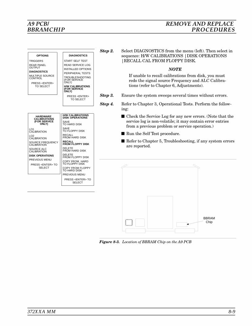
Step 2. Select DIAGNOSTICS from the menu (left). Then select insequence: H/W CALIBRATIONS |DISK OPERATIONS|RECALL CAL FROM FLOPPY DISK.
NOTEIf unable to recall calibrations from disk, you mustredo the signal source Frequency and ALC Calibra-tions (refer to Chapter 6, Adjustments).
Step 3. Ensure the system sweeps several times without errors.
Step 4. Refer to Chapter 3, Operational Tests. Perform the follow-ing:
Check the Service Log for any new errors. (Note that theservice log is non-volatile; it may contain error entriesfrom a previous problem or service operation.)
Run the Self Test procedure.
Refer to Chapter 5, Troubleshooting, if any system errorsare reported.
BBRAMChip
Figure 8-3. Location of BBRAM Chip on the A9 PCB
A9 PCB/ REMOVE AND REPLACE BBRAMCHIP PROCEDURES
OPTIONS
TRIGGERS
REAR PANEL OUTPUT
DIAGNOSTICS
MULTIPLE SOURCECONTROL
PRESS <ENTER>TO SELECT
DIAGNOSTICS
START SELF TEST
READ SERVICE LOG
INSTALLED OPTIONS
PERIPHERAL TESTS
TROUBLESHOOTING(FOR SERVICEONLY)
H/W CALIBRATIONS(FOR SERVICEONLY)
PRESS <ENTER>TO SELECT
HARDWARE CALIBRATIONS(FOR SERVICE
ONLY)
LO1CALIBRATION
LO2CALIBRATION
SOURCE FREQUENCY CALIBRATION
SOURCE ALC CALIBRATION
DISK OPERATIONS
PREVIOUS MENU
PRESS <ENTER> TOSELECT
H/W CALIBRATIONSDISK OPERATIONS
SAVETO HARD DISK
SAVETO FLOPPY DISK
RECALLFROM HARD DISK
RECALLFROM FLOPPY DISK
DELETEFROM HARD DISK
DELETEFROM FLOPPY DISK
COPY FROM HARDTO FLOPPY DISK
COPY FROM FLOPPYTO HARD DISK
PREVIOUS MENU
PRESS <ENTER> TOSELECT
372XXA MM 8-9

8-6 REMOVE / REPLACE A9PCB SRAM BATTERY
This paragraph provides instructions for removing and replacing theSRAM Battery located on the A9 Main Processor PCB assembly.
Preliminary:
Switch the 372XXA power off. Remove the power cord.
CAUTION
The SRAM battery incorporates flammable materials suchas lithium and organic solvents. If lithium batteries, suchas this one, are mistreated or incorrectly handled, theymay burst open and ignite. This can result in possible in-jury or fire. When handling the SRAM battery, carefully fol-lowing the following precautions:• DO NOT short circuit.• DO NOT disassemble, deform, or apply excessive pres-
sure.• DO NOT heat or incinerate.• DO NOT apply solder directly.• DO NOT mix model or new and old batteries.• DO NOT charge.• ALWAYS check that proper polarity is observed.
Remove/Replace Procedure:
Step 1. Remove the top cover and the large card-cage cover to ex-pose the A1 – A9 PCBs (refer to paragraph 8-3).
Step 2. Remove the A9 PCB from the unit.
Step 3. Locate and carefully remove the SRAM battery from the A9PCB. See Figure 8-4.
Step 4. Replace the SRAM battery on the A9 PCB, as follows: - Insure that the pins are clean. - Note the polarity and carefully press the batterly into the socket.
Step 5. Reinstall the A9 PCB, the large card-cage cover, and the topcover.
Post Replacement Procedure:
Step 1. Connect power cord. Switch 372XXA power on.
Step 2. Ensure the system sweeps several times without errors.
Step 3. Refer to Chapter 3, Operational Tests. Perform the follow-ing:
REMOVE AND REPLACE A9 PCB/PROCEDURES SRAM BATTERY
8-10 372XXA MM
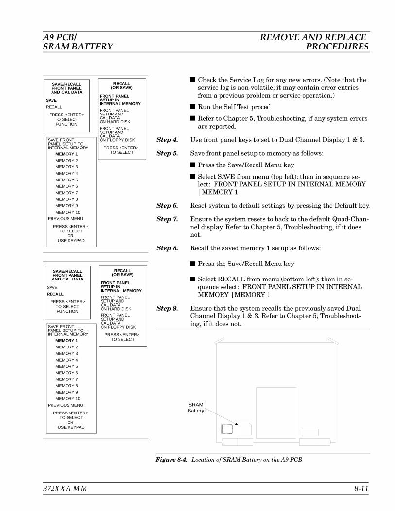
Check the Service Log for any new errors. (Note that theservice log is non-volatile; it may contain error entriesfrom a previous problem or service operation.)
Run the Self Test procedure.
Refer to Chapter 5, Troubleshooting, if any system errorsare reported.
Step 4. Use front panel keys to set to Dual Channel Display 1 & 3.
Step 5. Save front panel setup to memory as follows:
Press the Save/Recall Menu key
Select SAVE from menu (top left): then in sequence se-lect: FRONT PANEL SETUP IN INTERNAL MEMORY|MEMORY 1
Step 6. Reset system to default settings by pressing the Default key.
Step 7. Ensure the system resets to back to the default Quad-Chan-nel display. Refer to Chapter 5, Troubleshooting, if it doesnot.
Step 8. Recall the saved memory 1 setup as follows:
Press the Save/Recall Menu key
Select RECALL from menu (bottom left): then in se-quence select: FRONT PANEL SETUP IN INTERNALMEMORY |MEMORY 1
Step 9. Ensure that the system recalls the previously saved DualChannel Display 1 & 3. Refer to Chapter 5, Troubleshoot-ing, if it does not.
A9 PCB/ REMOVE AND REPLACE SRAM BATTERY PROCEDURES
SRAMBattery
Figure 8-4. Location of SRAM Battery on the A9 PCB
SAVE/RECALLFRONT PANELAND CAL DATA
SAVE
RECALL
PRESS <ENTER>TO SELECTFUNCTION
RECALL(OR SAVE)
FRONT PANELSETUP IN INTERNAL MEMORY
FRONT PANEL SETUP ANDCAL DATAON HARD DISK
FRONT PANEL SETUP ANDCAL DATAON FLOPPY DISK
PRESS <ENTER> TO SELECT
SAVE FRONTPANEL SETUP TOINTERNAL MEMORY
MEMORY 1
MEMORY 2
MEMORY 3
MEMORY 4
MEMORY 5
MEMORY 6
MEMORY 7
MEMORY 8
MEMORY 9
MEMORY 10
PREVIOUS MENU
PRESS <ENTER> TO SELECT
OR USE KEYPAD
372XXA MM 8-11
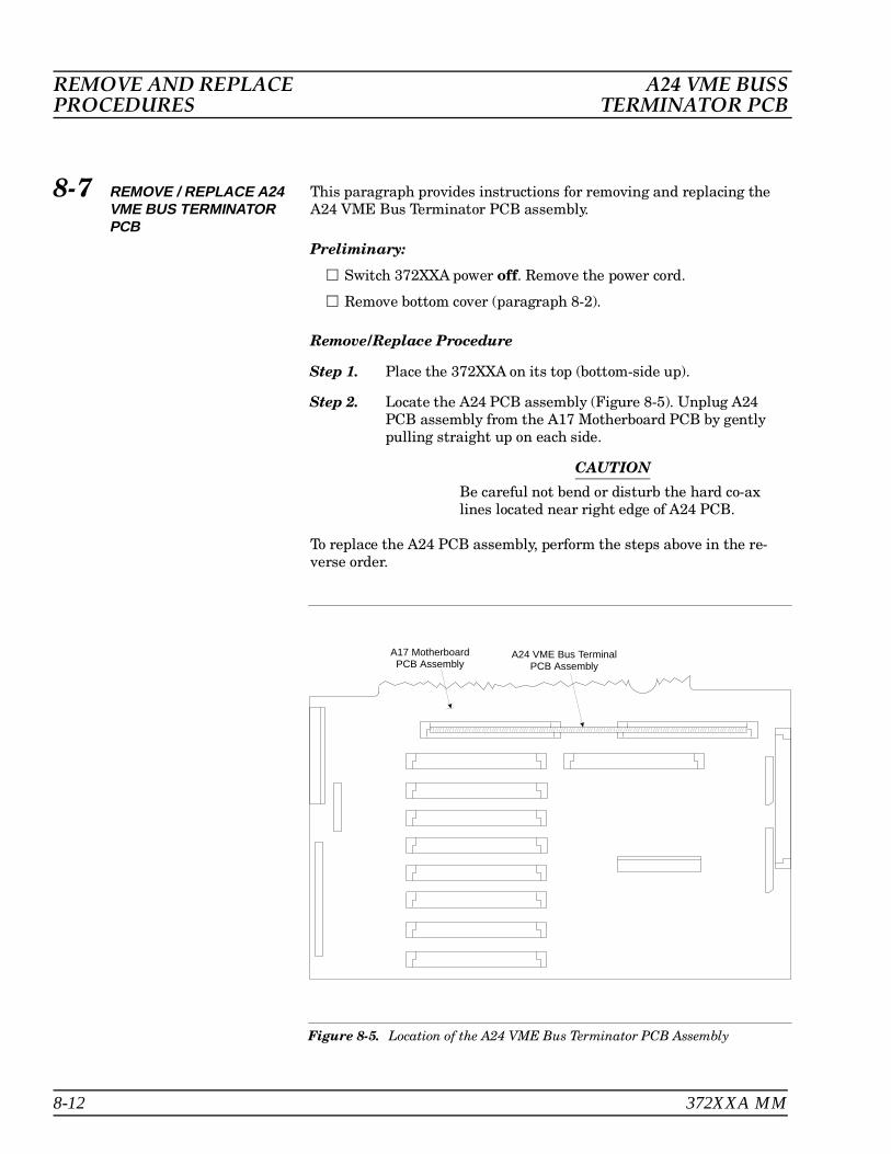
8-7 REMOVE / REPLACE A24VME BUS TERMINATORPCB
This paragraph provides instructions for removing and replacing theA24 VME Bus Terminator PCB assembly.
Preliminary:
Switch 372XXA power off. Remove the power cord.
Remove bottom cover (paragraph 8-2).
Remove/Replace Procedure
Step 1. Place the 372XXA on its top (bottom-side up).
Step 2. Locate the A24 PCB assembly (Figure 8-5). Unplug A24PCB assembly from the A17 Motherboard PCB by gentlypulling straight up on each side.
CAUTION
Be careful not bend or disturb the hard co-axlines located near right edge of A24 PCB.
To replace the A24 PCB assembly, perform the steps above in the re-verse order.
A24 VME Bus TerminalPCB Assembly
A17 MotherboardPCB Assembly
Figure 8-5. Location of the A24 VME Bus Terminator PCB Assembly
REMOVE AND REPLACE A24 VME BUSSPROCEDURES TERMINATOR PCB
8-12 372XXA MM

8-8 REMOVE / REPLACEFRONT PANELASSEMBLY
This paragraph provides instructions for removing and replacing the372XXA Front Panel assembly.
Equipment Required:Open-end wrench, 1 in.
Preliminary:
Switch 372XXA power off. Remove the power cord.
Remove handle assembles and all covers (paragraph 8-2).
Remove/Replace Procedure:
Step 1. Place the 372XXA in normal (top-side up) position.
Step 2. Remove the four corner screws and the top center screwthat secure the front panel assembly to the chassis (see Fig-ure 8-6).
Step 3. Place the 372XXA on its top (bottom-side up).
Step 4. Remove the screw that fastens the front panel casting ex-tension lip to the Test Set Module tray. (See diagram at left.)
Figure 8-6. Removal of Front Panel Assembly
FRONT PANEL REMOVE AND REPLACE ASSEMBLY PROCEDURES
372XXA MM 8-13

Step 5. Using a 1 in. open-end wrench, remove the nuts and wash-ers that secure the Port 1 and Port 2 couplers/bridges to thefront panel casting.
Step 6. Locate the cable from the front panel Power switch to con-nector J20 on the A17 Motherboard PCB. Disconnect atA17, J20 end.
Step 7. Locate the cable from the front panel Keyboard interfaceconnector to connector J16 on the A17 Motherboard PCB.Disconnect at A17, J16 end.
Step 8. Locate the cables from the front panel Bias Input BNC con-nectors to connector P2 on the A18 Rear Panel PCB. Discon-nect at A18, P2 end. (A18, P2 is the connector nearest to thebottom lip of the rear panel.)
Step 9. Gently pull front panel assembly several inches away fromchassis. Locate cable from A17 Motherboard PCB to connec-tor J1 on A20 Front Panel PCB. Disconnect at A20, J1 end.
Step 10. Separate the bias input cables (Step 8) from the cable har-nesses, as necessary for removal. Pull front panel assemblyfree and set aside.
To replace the front panel assembly, perform the steps above in the re-verse order.
8-9 REMOVE / REPLACE VGADISPLAY MONITOR
This paragraph provides instructions for removing and replacing the in-ternal VGA Display Monitor assembly.
NOTEIt is not necessary to remove the front panel assembly toperform this procedure.
Preliminary:
Switch 372XXA power off. Remove the power cord.
Remove all covers (paragraph 8-2).
Remove/Replace Procedure:
Step 1. Place the 372XXA on its right side (monitor down).
Step 2. At rear of monitor assembly, disconnect:
The power cord (from the Power Supply Module)
The data cable from motherboard CRT connector, J14
REMOVE AND REPLACE FRONT PANELPROCEDURES ASSEMBLY
8-14 372XXA MM

The two cables from motherboard BRITE/DEGAUSS con-nector, J15.
NOTEAll the the cables mentioned above have keyedconnectors.
Step 3. Remove the four screws that fasten the monitor assembly tothe chassis (see Figure 8-7). Do not unfasten the screwwith the blue plastic washer under the screw head.
Step 4. Gently move the monitor assembly to the rear and lift awayfrom chassis, with cables still attached. Place on work sur-face next to unit.
To replace the Internal VGA Display Monitor assembly, perform thesteps above in the reverse order.
VGA MONITOR REMOVE AND REPLACE DISPLAY ASSEMBLY PROCEDURES
J7
J2
TEST A
TEST B
J1
TP4
TP1
J2
TEST A
TEST B
J1
TP4
TP1
2 PL
2 PL
Figure 8-7. Location of Internal VGA Monitor Assembly Mounting Screws
372XXA MM 8-15

8-10 REMOVE / REPLACEFLOPPY DISK DRIVE
This paragraph provides instructions for removing and replacing theFloppy Disk Drive assembly.
NOTEIt is not necessary to remove the front panel assem-bly to perform this procedure.
Preliminary:
Switch 372XXA power off. Remove the power cord.
Remove all covers (paragraph 8-2).
NOTEAll the the cables mentioned in the following proce-dure have “keyed” connectors.
Remove/Replace Procedure:
Step 1. Place the 372XXA on its top (bottom-side up).
Step 2. At the floppy drive, disconnect the four-conductor DiskPower cable that connects to J1 of the motherboard PCB.
Step 3. At J2 on the motherboard PCB, disconnect the Floppy Con-trol (ribbon) cable that goes to the floppy drive.
Step 4. Remove the three screws that fasten the floppy disk drivemounting plate to the chassis and to the Test Set Moduletray (see Figure 8-8).
Step 5. Carefully pull the floppy disk drive assembly to the rearand up to remove assembly.
Step 6. Carefully remove the Floppy Control cable from the rear ofthe floppy drive. Set aside for re-use.
To replace the Floppy Disk Drive assembly, perform the steps above inthe reverse order.
REMOVE AND REPLACE FLOPPY DISKPROCEDURES DRIVE ASSEMBLY
8-16 372XXA MM

Figure 8-8. Location of Floppy Disk Drive Assembly Mounting Plate Screws
FLOPPY DISK REMOVE AND REPLACE DRIVE ASSEMBLY PROCEDURES
372XXA MM 8-17

8-11 REMOVE / REPLACEREAR PANELASSEMBLY
This paragraph provides instructions for removing and replacing theRear Panel Assembly.
Equipment Required Option 11 only):Connector torque wrench (5⁄16 in), WILTRON Model 01-201, orequivalent.
Preliminary:
Switch 372XXA power off. Remove the power cord.
Remove all covers (paragraph 8-2).
Remove/Replace Procedure:
Step 1. Place the 372XXA in normal (top-side up) position.
Step 2. Remove the three screws on each side of the chassis thatfasten to the rear panel assembly. See Figure 8-9.
Step 3. Remove the two screws located near top and middle of rearpanel (near fan-mounting screws). See Figure 8-9.
REMOVE AND REPLACE REAR PANELPROCEDURES ASSEMBLY
External I/O
Reference Extension
RA In RB In RB Out
Display
IEEE 488.2 GPIB
10 MHz Ref
Εξτ ExtTrigger
ExtAnlg In
100-120V 5A SB
SAME TYPE AND RATING
85-264VAC48-63HzREPLACE FUSE ONLY WITH
540VA MAX
220-240V 2.5A SB
Bias FusesPort 1 Port 2
VGA OUT
Printer Out
CRT Degauss CRT Brt
WARNINGNO OPERATOR SERVICE-ABLE PARTS INSIDEREFER SERVICING TO
QUALIFIED PERSONNEL
CAUTIONFOR CONTINUED FIREPROTECTION REPLACEONLY WITH SPECIFIEDTYPE AND RATED FUSE
SH
1
AH
1
T6
L4
SR
1
RL1
PP
1
DC
1
DT
1
C0
E2
Refer to manualfor GPIB address
RAOutFUSE
FUSEFU
SE
FUSE
FUSEFU
SE
1n ±5dBm 50 Ω Out 0dBm 50 Ω
ExtAnlg Out
1
24 PL
1
13 3
4
Rear Panel Assembly screws (par 8-11)Fan Assembly screws (par 8-12)Power Supply Assembly screws (par 8-13)A18 Rear Panel PCB screw (par 8-14)
1234
Figure 8-9. Location of Mounting Screws for Rear Panel Assemblies
8-18 372XXA MM

Step 4. Locate cable from the rear-panel 10 MHz Ref In BNC con-nector to connector J2 of A7 PCB. Disconnect at A7, J2 end.(Pull up gently to disconnect.)
Step 5. Locate cable from the rear-panel 10 MHz Ref Out BNC con-nector to connector J3 of A7 PCB. Disconnect at A7, J3 end.
Step 6. Locate cable from the rear-panel Ext Anlg In BNC connec-tor to connector J1 of A5 PCB. Disconnect at A5, J1 end.
Step 7. Place the 372XXA on its right side (monitor down).
Step 8. Locate the cables from the rear-panel Ext Trigger and ExtAnlg Out BNC connectors to connector P13 of the A18 RearPanel PCB. Disconnect at A18, P13 end. (A18, P3 is thefourth connector away from the rear panel bottom lip.)
Step 9. Disconnect the large ribbon cable from connector P1 of theA18 PCB at motherboard connector J12.
Step 10. Disconnect the two cables from the Power Supply Module atmotherboard connectors J4 and J13.
Step 11. Disconnect power cord from the Power Supply Module tothe internal VGA Display Monitor at the display monitor.
Step 12. If 372XXA is equipped with Option 11, Reference Loop Ex-tension Cables:
Using a 5⁄16 in. wrench, disconnect the External Refer-ence Loops from the rear panel connectors.
Using a 5⁄16 in. wrench, disconnect the semi-rigid coaxiallines W44, W45, W46, and W47 at the inside of the rearpanel. See Figure 8-11 on page 8-24.
Step 13. If 372XXA is equipped with Option 10, High Stability TimeBase:
Locate output cable from the high stability oscillator as-sembly (mounted above Power supply Module) to connec-tor J1 of A7 PCB. Disconnect at A7, J1 end.
Locate power cable from the high stability oscillator as-sembly to A17 Motherboard connector, J18. Disconnect atA17, J18 end.
Step 14. Place the 372XXA in normal (top-side up) position. Gentlypull rear panel assembly away from chassis and lay flat onwork surface. Remove cables from cable harnesses, as re-quired.
To replace the Rear Panel Assembly, perform the steps above in the re-verse order.
REAR PANEL REMOVE AND REPLACE ASSEMBLY PROCEDURES
372XXA MM 8-19

8-12 REMOVE / REPLACEFAN ASSEMBLY
This paragraph provides instructions for removing and replacing theRear Panel Fan Assembly.
Preliminary:
Switch 372XXA power off. Remove the power cord.
Remove all covers (paragraph 8-2).
Remove Rear Panel (paragraph 8-10).
Remove/Replace Procedure:
Step 1. Place the Rear Panel Assembly on the work surface withthe A18 Rear Panel PCB up.
Step 2. Disconnect the two conductor fan power cable at connectorP6 of the A18 PCB.
Step 3. Turn Rear Panel Assembly over, and remove the four screwsthat fasten the fan guard and fan assembly to the rearpanel. See Figure 8-9.
Step 4. Remove the fan guard and separate the fan from the rearpanel.
To replace the Rear Panel Fan Assembly, perform the steps above inthe reverse order.
8-13 REMOVE / REPLACEPOWER SUPPLYMODULE
This paragraph provides instructions for removing and replacing thePower Supply Module.
Preliminary:
Switch 372XXA power off. Remove the power cord.
Remove all covers (paragraph 8-2).
Remove Rear Panel (paragraph 8-10).
Remove/Replace Procedure:
Step 1. Place the Rear Panel Assembly on the work surface withthe Power Supply Module down.
Step 2. Remove the six screws from the rear panel that fasten it tothe left and right edges of the Power Supply Module (seeFigure 8-9). Gently separate the two units.
To replace the Power Supply Module, perform the steps above in the re-verse order.
REMOVE AND REPLACE FAN ASSEMBLY/PROCEDURES POWER SUPPLY MODULE
8-20 372XXA MM

8-14 REMOVE / REPLACEA18 REAR PANEL PCB
This paragraph provides instructions for removing and replacing theA18 Rear Panel PCB assembly.
Equipment Required:
Nut Driver, 9⁄32 in.
Nut Driver, 3⁄16 in.
Preliminary:
Switch 372XXA power off. Remove the power cord.
Remove all covers (paragraph 8-2).
Remove Rear Panel (paragraph 8-10).
Remove/Replace Procedure:
Step 1. Place the Rear Panel Assembly on the work surface withthe A18 Rear Panel PCB up.
Step 2. Disconnect the two-conductor fan power cable at connectorP6 of the A18 PCB.
Step 3. Disconnect the wiring for the rear panel Bias Fuses at con-nector P4 of the A18 PCB.
Step 4. Turn Rear Panel Assembly over. Remove screw located atlower left corner of the rear panel that fastens the A18 PCBto the Rear Panel Assembly (see Figure 8-9).
Step 5. Using a 9⁄32 in. nut driver, remove the standoffs that fastenthe IEEE 488.2 GPIB and Dedicated GPIB connectors tothe rear panel.
Step 6. Using a 3⁄16 in. nut driver, remove the standoffs that fastenthe Printer Out, VGA Out, and External/IO connectorsto the rear panel. Set standoffs aside for re-use.
Step 7. Carefully separate the A18 PCB from the rear panel.
To replace the A18 Rear Panel PCB assembly, perform the steps abovein the reverse order.
A18 REAR PANEL REMOVE AND REPLACE PCB ASSEMBLY PROCEDURES
372XXA MM 8-21
8-15 REMOVE / REPLACETEST SET MODULEASSEMBLIES
The following paragraphs provide instructions for removing and replac-ing the RF/microwave components that comprise the Test Set Module .
Equipment Required:Connector torque wrench (5⁄16 in), WILTRON Model 01-201, orequivalent. Open-end wrench, 1 in.
CAUTION
Throughout these procedures, always use the 5⁄16 in. con-nector torque wrench for connecting the Test Set Modulesemi-rigid coaxial lines and RF/microwave components.Use of improper tools may damage the connectors, result-ing in degraded instrument performance.
Preliminary:
Switch 372XXA power off. Remove the power cord.
Remove all covers (paragraph 8-2).
Transfer Switch Use the following procedure to remove/replace the Transfer Switch,which is common to all 372XXA models.
Procedure:
Step 1. For all models except 37269A: disconnect the semi-rigid co-axial line W87 from the input connector of the TransferSwitch. See Figure 8-10.
For Model 37269A: loosen the two screws that fasten theTransfer Switch mounting plate to the test set tray beforedisconnecting the semi-rigid coaxial line (W80). See Fig-ure 8-11.
Step 2. Disconnect the right and left Level Detector assembliesfrom the Transfer switch.
Step 3. Carefully flex (do not bend) the Level Detector rigid-coaxiallines to gain access to the lower connectors of the TransferSwitch; see Inset A on Figure 8-10. Remove rigid-coaxiallines W86 and W89 from these connectors.
Step 4. Disconnect the Transfer Switch power cable at connector J5of the A17 Motherboard PCB. Free the cable by separatingit from the cable harness and by temporarily removing theA24 VME Terminator PCB.
REMOVE AND REPLACE TEST SET MODULEPROCEDURES ASSEMBLIES
8-22 372XXA MM
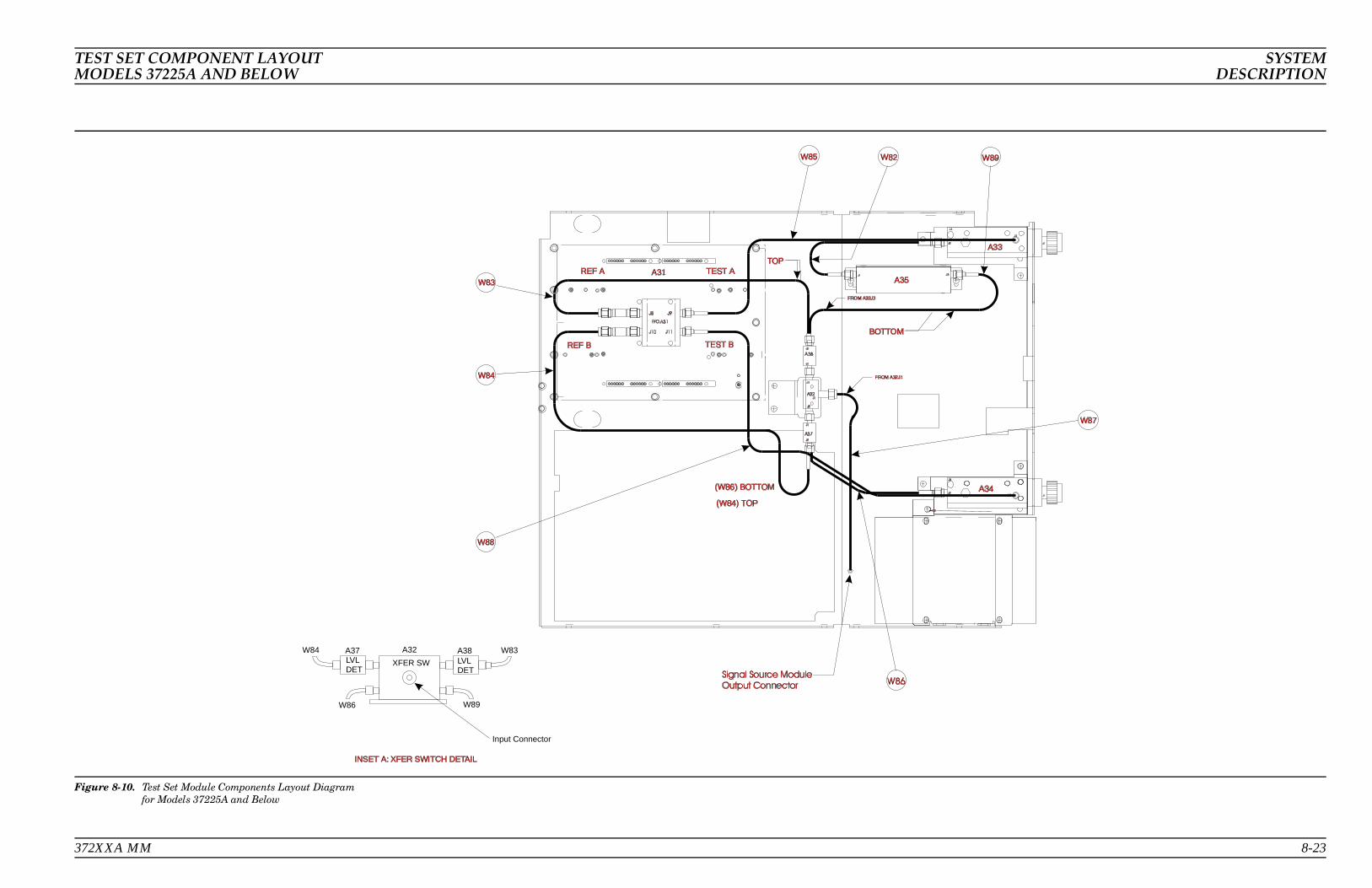
W84
W83
W85 W82
W86Signal Source Module
Output Connector
W87
W89
A31
J8
J10
J9
J11
A38
A37
J1
J1
J2
J2
A32J1
J2
J3
A33J1J2
J3
J4
A35J1 J2
A34J1
J2
J4
J3
P/O A31
FROM A32J1
FROM A32J3
REF A TEST A
REF B TEST B
(W84) TOP
(W86) BOTTOM
TOP
W88
BOTTOM
W84LVLDET
LVLDET
XFER SW
A37 A32 A38 W83
W89
Input Connector
INSET A: XFER SWITCH DETAIL
W86
Figure 8-10. Test Set Module Components Layout Diagram for Models 37225A and Below
TEST SET COMPONENT LAYOUT SYSTEMMODELS 37225A AND BELOW DESCRIPTION
372XXA MM 8-23

W85 W82
W88
W89
A31W44
W47
W46
W45
A37
A38
J1
A32
J1
J2
J3
A33J1J2
J3J4
A35 J2
A34 J1J2
J4
J3
TOP
(W86) BOTTOM
A31J8
A31J10
A31J9
A31J11
A35J2
A37
J1
A38
J2
A37J2
A38J2
A36A36J2
A36J1
W80Signal Source ModuleOutput Connector W86
A34J2
Port 2 StepAtten (Opt. 6)
A34J3
A33J3
A32J1
W81
TOP
BOTTOM
Figure 8-11. Test Set Module Components Layout Diagram for Model 37269A (with Options 6 and 11)
8-24 372XXA MM
SYSTEM TEST SET COMPONENT LAYOUTDESCRIPTION MODEL 37269A

Step 5. Remove the two screws that fasten the Transfer Switchmounting plate to the test set tray, and lift the TransferSwitch assembly from the Test Set Module.
To replace the Transfer Switch assembly, perform the steps above inthe reverse order.
Level Detectors Use the following procedure to remove/replace the Level Detectors,which are common to all 372XXA models.
NOTEReplacement Level Detectors are supplied as a pre-wiredset, PN C24950-1.
Procedure:
Step 1. Disconnect the Level Detector power cable at connector J3of the A21A2 Source Control PCB.
Step 2. Disconnect the semi-rigid coaxial lines, W83 and W84,from the right and left Level Detectors (see Figure 8-10).
Step 3. Disconnect the right and left Level Detector assembliesfrom the Transfer Switch. Remove carefully from the TestSet Module.
To replace the Level Detectors, perform the steps above in the reverseorder.
Port1 SourceStep Attenuator
Use the following procedure to remove/replace the Port1 Source StepAttenuator assembly which is common to all 372XXA models.
Procedure:
Step 1. Disconnect the semi-rigid coaxial lines, W89 and W82*,from the input and output connectors of the Port1 SourceStep Attenuator (see Figure 8-10).
Step 2. Disconnect the Port1 Source Step Attenuator power cableat connector J11 of the A17 Motherboard PCB.
Step 3. Remove the two screws that fasten the attenuator assemblyto the test set tray, and lift the assembly from the Test SetModule.
To replace the Port1 Source Step Attenuator assembly, perform thesteps above in the reverse order.
∗ W111 for Models 37211A and 37217A
TEST SET MODULE REMOVE AND REPLACE ASSEMBLIES PROCEDURES
372XXA MM 8-25

Input Coupler(s)/Low Freq Bridge(s)
Use the following procedure to remove/replace the Input Coupler(s) ofall models 37225A through 37269A and the Low Frequency Bridges ofmodels 37211A and 37217A.
Procedure:
Step 1. Using a 1 in. open-end wrench, remove the front panel nutand washer of the Port1or Port2 coupler/bridge that is tobe removed.
Step 2. Disconnect the two semi-rigid coaxial lines associated withthe coupler/bridge (see Figure 8-10).
Step 3. Disconnect/desolder coaxial line at the bias tee control in-put of couplers/bridges.
Step 4. Remove the two screws that fasten the coupler/bridgebracket to the test set tray. Move coupler/bridge to the rearand up to remove it from the Test Set Module.
To replace the coupler/bridge, perform the steps above in the reverseorder.
Power Amplifier Use the following procedure to remove/replace the Power Amplifier as-sembly, which is common to all 372XXA models.
Procedure:
Step 1. Disconnect the Power Amplifier power cable at connector J5of the A17 Motherboard PCB. Free the cable by separatingit from the cable harness and by temporarily removing theA24 VME Terminator PCB.
Step 2. Disconnect the PWR AMP IN cable on the side of the PowerAmplifier assembly; see Figure 8-12. (Pull out gently to dis-connect.)
Step 3. Remove the two screws that fasten the Power Amplifier as-sembly to the test set tray. Remove the two screws that fas-tens the assembly feet to the Buffer Amplifier/Sampler as-sembly.
Step 4. Disconnect the Power Amplifier from the Buffer Ampli-fier/Sampler by carefully pulling up on the connector end ofthe rigid-coaxial line from the Power Amplifier. (See Fig-ure 8-12.) Carefully lift the assembly from the Test Set Mod-ule.
To replace the Power Amplifier assembly, perform the steps above inthe reverse order.
REMOVE AND REPLACE TEST SET MODULEPROCEDURES ASSEMBLIES
8-26 372XXA MM

TEST SET MODULE REMOVE AND REPLACE ASSEMBLIES PROCEDURES
Power AmpIn Cable
Power CableOutput Connector
Rigid Coax Line
A41 Power Amp Assy
P/O Buff Amp/Sampler (A31)
Figure 8-12. A41 Power Amplifier Assembly, Details
372XXA MM 8-27

Buffer Amplifier/Sampler(A31)
Use the following procedure to remove/replace the Buffer Amplifier/Sampler assemblies of all models.
Preliminary:
Remove the Power Amplifier assembly (see previous paragraph).
Procedure:
Step 1. Disconnect the semi-rigid coaxial lines, W83 and W84, fromthe 20 dB pads that are part of the Buffer Amplifier/Sam-pler assembly; see Figure 8-13. (For units with Option 11,the semi-rigid coaxial lines are W46 and W47.)
Step 2. Disconnect the cables from connectors J1 through J7 of theA31 Buffer Amplifier/Sampler assembly. (Pull up gently todisconnect.) Note that the connector end of each cable ismarked with the associated A31 connector number.
Step 3. Disconnect the two cable connectors from the TEST A con-nector body on the Buffer Amplifier/Sampler assembly (seeFigure 8-13). Similarly, disconnect the two cable connectorsfrom the REF A connector body.
NOTEThe matching pin numbers are identified on the ca-ble connectors and on the connector body.)
Step 4. Repeat Step 3 for the TEST B and REF B cable connectors.
Step 5. Remove the nine screws that fasten the Buffer Ampli-fier/Sampler assembly to the test set tray, and lift the as-sembly from the Test Set Module.
To replace the Buffer Amplifier/Sampler assembly, perform the stepsabove in the reverse order.
REMOVE AND REPLACE TEST SET MODULEPROCEDURES ASSEMBLIES
8-28 372XXA MM

REF AConnector BodyA31J8
REF AConnector Body
A31J10
W84
J1J2
J3
J4
J5
J6J7
W83
REF A
REF B
TEST A
TEST B
TEST AConnector Body
TEST AConnector Body
Figure 8-13. A31 Buffer Amplifier/Sampler Assembly, Details
TEST SET MODULE REMOVE AND REPLACE ASSEMBLIES PROCEDURES
372XXA MM 8-29

Switched DoublerModule Assembly
Use the following procedure to remove/replace the Switched DoublerModule (SDM) assembly for Model 37269A.
Procedure:
Step 1. Disconnect the SDM power cable from connector J17 of theA17 Motherboard PCB. Free cable from cable clip, as neces-sary.
Step 2. Disconnect the semi-rigid coaxial line W81 from the inputconnector of the SDM; see Figure 8-11.
Step 3. Remove the two screws that fasten the SDM to the Test SetModule tray.
Step 4. Disconnect the semi-rigid coaxial line W80 from the outputconnector of the SDM; see Figure 8-11. Carefully lift the as-sembly from the Test Set Module.
To replace the Switched Doubler Module assembly, perform the stepsabove in the reverse order.
Port 2 Step Attenu-ator (Opt 6)
Use the following procedure to remove/replace the Port 2 Step Attenu-ator assembly for units equipped with Option 6.
Procedure:
Step 1. Disconnect the Port 2 Step Attenuator power cable from con-nector J10 of the A17 Motherboard PCB. Free cable from ca-ble clip, as necessary.
Step 2. Disconnect the semi-rigid coaxial lines from the input andoutput connectors of the step attenuator assembly; see Fig-ure 8-11.
Step 3. Remove the two screws that fasten the step attenuatorassembly to the Test Set Module tray. Carefully lift the as-sembly from the Test Set Module.
To replace the Port 2 Step Attenuator assembly, perform the stepsabove in the reverse order.
REMOVE AND REPLACE TEST SET MODULEPROCEDURES ASSEMBLIES
8-30 372XXA MM

8-16 REMOVE / REPLACESIGNAL SOURCEMODULE ASSEMBLIES
The following paragraphs provide instructions for removing and replac-ing the RF/microwave components that comprise the Signal SourceModule.
Equipment Required:Connector torque wrench (5⁄16 in), WILTRON Model 01-201, orequivalent.
CAUTION
Throughout these procedures, always use the 5⁄16 in. con-nector torque wrench for connecting the Signal Source Mod-ule semi-rigid coaxial lines and rf/microwave components.Use of improper tools may damage the connectors, result-ing in degraded instrument performance.
Preliminary:
Switch 372XXA power off. Remove the power cord.
Remove all covers (paragraph 8-2).
Removal of SignalSource Module
Use the following procedure to remove the Signal Source Module fromthe chassis. This step is necessary before any of the module compo-nents can be removed/replaced.
Procedure:
Step 1. Place the 372XXA on its top (bottom-side up).
Step 2. At J2 on the motherboard PCB, disconnect the Floppy Con-trol (ribbon) cable that goes to the floppy drive. Dress theribbon cable away from the Signal Source Module outputconnector; see Figure 8-10.
Step 3. Disconnect the semi-rigid coaxial line W87* from the outputconnector of the Signal Source Module.
Step 4. Place the 372XXA in normal (top-side up) position.
Step 5. Disconnect the cables from connectors J1 and J2 of theA21A2 Source Control PCB. (Pull up gently to disconnect.)Note that the connector end of each cable is marked withthe associated A21A2 connector number.
Step 6. Disconnect the cable from connector J3** of the A21A2Source Control PCB. Dress cables away from the SignalSource Module.
SIGNAL SOURCE REMOVE AND REPLACE MODULE ASSEMBLIES PROCEDURES
∗ W81 for Models 37269A ∗∗ Never operate unit with A21A2, J3 disconnected. Refer to Caution statement on
Page 5-2.
372XXA MM 8-31

Step 7. Remove the three screws that fasten the Signal Source Mod-ule to the chassis side rail. See Figure 8-14.
Step 8. Loosen the two captive screws that fasten the Signal SourceModule to the chassis (Figure 8-14).
Step 9. Pull up at the rear of the Signal Source Module to discon-nect the A21A1 Source YIG Bias Control PCB from the A17Motherboard PCB. Lift the module from the chassis andplace on work surface.
To replace the Signal Source Module, perform the steps above in the re-verse order.
Side Rail MountingScrews
Captive Screws
A21A2 SourceControl PCB
Figure 8-14. Signal Source Module Removal Details
REMOVE AND REPLACE SIGNAL SOURCEPROCEDURES MODULE ASSEMBLIES
8-32 372XXA MM
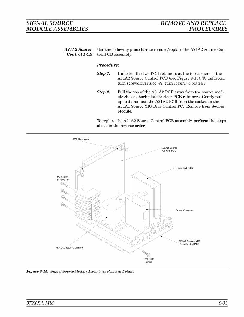
A21A2 SourceControl PCB
Use the following procedure to remove/replace the A21A2 Source Con-trol PCB assembly.
Procedure:
Step 1. Unfasten the two PCB retainers at the top corners of theA21A2 Source Control PCB (see Figure 8-15). To unfasten,turn screwdriver slot 1⁄4 turn counter-clockwise.
Step 2. Pull the top of the A21A2 PCB away from the source mod-ule chassis back plate to clear PCB retainers. Gently pullup to disconnect the A21A2 PCB from the socket on theA21A1 Source YIG Bias Control PC. Remove from SourceModule.
To replace the A21A2 Source Control PCB assembly, perform the stepsabove in the reverse order.
Switched Filter
A21A2 SourceControl PCB
Down Converter
A21A1 Source YIGBias Control PCB
YIG Oscillator Assembly
Heat SinkScrew
Heat SinkScrews (4)
PCB Retainers
Figure 8-15. Signal Source Module Assemblies Removal Details
SIGNAL SOURCE REMOVE AND REPLACE MODULE ASSEMBLIES PROCEDURES
372XXA MM 8-33

A21A1 Source YIGBias Control PCB
Use the following procedure to remove/replace the A21A1 Source YIGBias Control PCB assembly.
Procedure:
Step 1. Disconnect the Switched Filter assembly power cable fromconnector J1 of the A21A1 Source YIG Bias Control PCB.(Pull up gently on ribbon cable to disconnect.)
Step 2. Similarly, disconnect the Down Converter assembly powercable from connector J4 of the A21A1 PCB.
Step 3. Disconnect the YIG Oscillator assembly power cable fromconnector J3 of the A21A1 PCB. Pull up on the flexible cir-cuit connector “handle” to disconnect.
Step 4. Remove the screw that fastens the front apron of the sourcemodule chassis to the heatsink of the A21A1 PCB. See Fig-ure 8-15.
Step 5. Remove the four screws that fastens the back plate of thesource module chassis to the heatsink of the A21A1 PCB.
Step 6. Place the Signal Source Module on its’ back plate.
Step 7. Unfasten the six PCB retainers on the bottom of the A21A1PCB. (To unfasten, turn screwdriver slot 1⁄4 turn counter-clockwise.) Gently separate the A21A1 PCB (including theheat sink) from the Signal Source Module.
To replace the A21A1 Source YIG Bias Control PCB assembly, performthe steps above in the reverse order.
Switched FilterAssembly
Use the following procedure to remove/replace the Switched Filter as-sembly.
Procedure:
Step 1. Disconnect the power cable from connector P1 at the rear ofthe Switched Filter assembly. (Use a small screw driver topry up gently at each end of the connector, as necessary.)
Step 2. Disconnect the semi-rigid coaxial lines from connector J6(top) and connector J3 (lower-front) of the Switched Filterassembly.
Step 3. Disconnect the semi-rigid coaxial line from the RF INPUT(top) connector of the Down Converter assembly.
Step 4. Remove the two screws that fasten the Switched Filter as-sembly to the source module chassis and lift the assemblyfrom the Signal Source Module.
REMOVE AND REPLACE SIGNAL SOURCEPROCEDURES MODULE ASSEMBLIES
8-34 372XXA MM
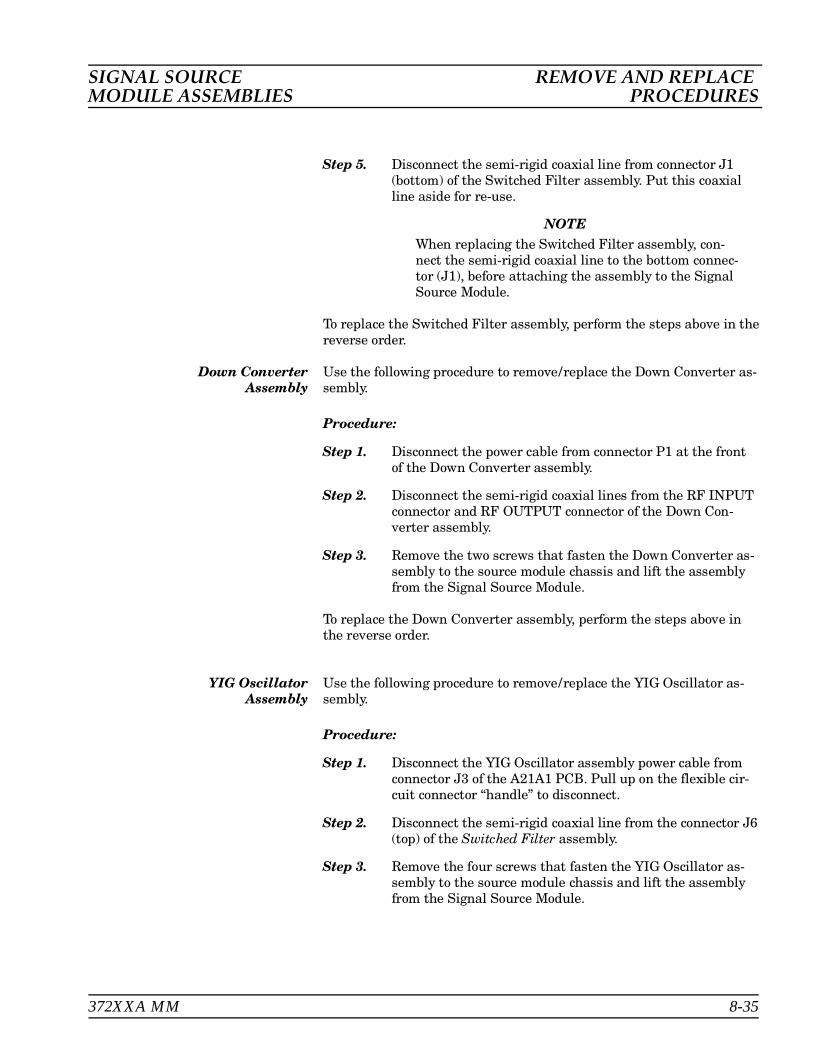
Step 5. Disconnect the semi-rigid coaxial line from connector J1(bottom) of the Switched Filter assembly. Put this coaxialline aside for re-use.
NOTEWhen replacing the Switched Filter assembly, con-nect the semi-rigid coaxial line to the bottom connec-tor (J1), before attaching the assembly to the SignalSource Module.
To replace the Switched Filter assembly, perform the steps above in thereverse order.
Down ConverterAssembly
Use the following procedure to remove/replace the Down Converter as-sembly.
Procedure:
Step 1. Disconnect the power cable from connector P1 at the frontof the Down Converter assembly.
Step 2. Disconnect the semi-rigid coaxial lines from the RF INPUTconnector and RF OUTPUT connector of the Down Con-verter assembly.
Step 3. Remove the two screws that fasten the Down Converter as-sembly to the source module chassis and lift the assemblyfrom the Signal Source Module.
To replace the Down Converter assembly, perform the steps above inthe reverse order.
YIG OscillatorAssembly
Use the following procedure to remove/replace the YIG Oscillator as-sembly.
Procedure:
Step 1. Disconnect the YIG Oscillator assembly power cable fromconnector J3 of the A21A1 PCB. Pull up on the flexible cir-cuit connector “handle” to disconnect.
Step 2. Disconnect the semi-rigid coaxial line from the connector J6(top) of the Switched Filter assembly.
Step 3. Remove the four screws that fasten the YIG Oscillator as-sembly to the source module chassis and lift the assemblyfrom the Signal Source Module.
SIGNAL SOURCE REMOVE AND REPLACE MODULE ASSEMBLIES PROCEDURES
372XXA MM 8-35

Step 4. Disconnect the semi-rigid coaxial line from the output con-nector of the YIG Oscillator assembly. Put this coaxial lineaside for re-use.
NOTEWhen replacing the YIG Oscillator assembly, con-nect the semi-rigid coaxial line removed in Step 4 tothe output connector of the YIG Oscillator before at-taching it to the Signal Source Module.
To replace the YIG Oscillator assembly, perform the steps above in thereverse order.
REMOVE AND REPLACE SIGNAL SOURCEPROCEDURES MODULE ASSEMBLIES
8-36 372XXA MM

Table of Contents
A-1 INTRODUCTION . . . . . . . . . . . . . . . . . . A-3
A-2 DIAGNOSTICS MENUS . . . . . . . . . . . . . . A-3
Start Self Test . . . . . . . . . . . . . . . . . . A-3Read Service Log . . . . . . . . . . . . . . . . A-3Installed Options . . . . . . . . . . . . . . . . A-4Peripheral Tests . . . . . . . . . . . . . . . . . A-4Troubleshooting . . . . . . . . . . . . . . . . . A-4H/W Calibrations . . . . . . . . . . . . . . . . A-5
Appendix ADiagnostics Menus

Appendix ADiagnostics Menus
A-1 INTRODUCTION This appendix contains descriptions and usage information for the372XXA Diagnostic Menus that are available via the front panel Op-tion Menu key.
A-2 DIAGNOSTICS MENUS The internal diagnostic capabilities of the 372XXA are accessed via theOptions Menu key, which is part of the front panel Enhancement keygroup. The selections available from the top level DIAGNOSTICSmenu (DG1) are listed below. See Figure A-1.
Start Self Test
Read Service Log
Installed Options
Peripheral Tests
Troubleshooting
H/W Calibrations
Start Self Test The START SELF TEST selection, when invoked, will automaticallytest circuits throughout the 372XXA. Once invoked, it requires no ex-ternal devices or interaction by the user. The net pass/fail result of theself-test is written to the CRT screen. Any self test failures will causedetailed failure information to be written into the service log.
This menu is available to service and non-service personnel.
Read Service Log The READ SERVICE LOG menu allows for viewing, printing, clearing,and saving the internal system service log to floppy disk. The CLEARLOG function is not recommended for non-service personnel.
The Service Log is made up of two parts, the log header and the errorlisting. The log header contains key system parameters such as initialsystem turn-on date/time/temperature, current power-on date/time/temperature, total operational hours, system model, serial, and in-stalled option numbers, date/time/temperature stamp of current serv-ice log viewing session, date/time/temperature of internal hardwarecalibrations, and statistics about various internal system phase lockingactivities.
The error listing is a time ordered log containing the system faultswith details about the system condition at the time of the fault.
372XXA MM A-3

NOTEThe service log must always be printed out or saved todisk and sent to the factory along with a failed assem-bly. Due to the importance of the information providedby the service log to WILTRON factory Service Engi-neers, the exchange prices are only valid if the servicelog data (disk or printout) is submitted to the factorywith the failed assembly.
This menu is available to service and non-service personnel. However,the service log should be cleared by service personnel only.
Installed Options The INSTALLED OPTIONS menu lists installed option numbers anddescriptions.
This menu is available to service and non-service personnel.
Peripheral Tests The PERIPHERAL TESTS menu (DG3) tests the printer and GPIBports, internal VGA monitor, front panel operation, and the externalIBM compatible keyboard (if keyboard is connected). These tests willrequire some interaction and external devices such as the Printer TestConnector (WILTRON PN: B39553), a GPIB cable, and an externalIBM compatible keyboard as appropriate for the specific test.
This menu is available to service and non-service personnel.
Troubleshooting The TROUBLESHOOTING menu (DG4) and its sub-menus provide ahost of pre-defined internal system modes and sub-system monitorsthat provide information useful in evaluating proper system operation.Most of these modes do not require any interaction or external test fix-tures. (An exception is the FIRST IF BANDPASS selection which re-quires a thru line to be connected between the test ports.)
Menu DG4A and its sub-menus provide low level access to internal sys-tem hardware. These menus allow the user to control system latches,switches, and DACs. They also allow selection of key system statessuch as set-on or search for lock. Many internal analog voltages maybe monitored via the 372XXA built-in DVM monitor network.
CAUTION
Always exit the troubleshooting mode via the DG4menu selection FINISHED, RECOVER FROMTROUBLESHOOTING to insure proper system staterecovery from your troubleshooting activities.
These menus are for service personnel only.
APPENDIX A DIAGNOSTICS MENUS
A-4 372XXA MM

H/W Calibrations The H/W CALIBRATIONS menus perform various internal automatedhardware calibrations, including ALC and Frequency calibrations. Thefollowing equipment is required for these tests:
HP 437B Power Meter (or Gigatronics 8541/42 Power Meter)
EIP 20 GHz series counter w/ GPIB (Option -08)
You need only connect the power meter or counter appropriate for the372XXA model, invoke the calibration desired, and wait until complete.The ALC and Frequency calibrations take 5 to 10 minutes each. SeeChapter 6, Adjustments, for further information.
The disk operations allow storage and retrieval of internal hardwarecalibration data to and from floppy disk. This feature will be usefulwhen replacing the A9 Processor PCB since it contains the BatteryBacked RAM where the internal hardware calibration data resides.
Automated field calibrations for the LO1 and LO2 assemblies are notpresently implemented. Should these assemblies fail or require any ad-justment, they must be replaced under the exchange assembly pro-gram (refer to Chapter 1).
These menus are for service personnel only.
372XXA MM A-5/A-6
DIAGNOSTICS MENUS APPENDIX A

HORIZONTAL
VERTICAL
PHASE LOCK
SELECT MODEFOR OUTPUT
PRESS <ENTER>TO SELECT
M EN U OR P2
PR ESS <E NTER>TO SELECT
ME NU DG4
TROUBLESHOOTING(FOR SERVICE USE ONLY)
LO1
LO2
SOURCE
NON-RATIOEDPARAMETERS
FIRST I.F.BANDPASS
MORE
FINISHED,RECOVER FROMTROUBLESHOOTING
EXTERNALA/D INPUT
PRESS <ENTER>TO SELECT
MENU DG4_LO2
MAIN PHASE LOCK VOLTAGE
MAIN D/A VOLTAGE
PREVIOUS MENU
OFFSET D/A VOLTAGE
OFFSET PHASE LOCK VOLTAGE
TROUBLESHOOTINGLO2
DDS PHASE LOCK VOLTAGE
PRESS <ENTER>TO SELECT
ME NU DG4_SO URCE
TROUBLESHOOTINGSOURCE
SOURCE LINEARITYVOLTAGE
POWER OUTPUT VOLTAGE
PREVIOUS MENU
ME N U OM1
DEFINE BANDS
OFF
DEFINE
ON
MULTIPLESOURCE CONTROL
MULTIPLESOURCE MODE
PRESS <ENTER>TO SELECT
PRINT LOG
SAVE LOGTO FLOPPY DISK
PRESS <ENTER>TO SELECT
MENU DG2
SERVICE LOG
DISPLAY LOG
CLEAR LOG
PREVIOUS MENU
PRESS <ENTER>TO SELECT
MENU DG5_SRC
PREVIOUS MENU
HARDWARECALIBRATION(FOR SERVICEUSE ONLY)
START SOURCEFREQ CALIBRATION
ME NU O PTNS
OPTIONS
TRIGGERS
DIAGNOSTICS
PRESS <ENTER>TO SELECT
MULTIPLESOURCE CONTROL
REAR PANELOUTPUT
PRESS <ENTER>TO SELECT
MENU DG5_ALC
PREVIOUS MENU
HARDWARECALIBRATION(FOR SERVICEUSE ONLY)
START ALCFREQ CALIBRATION
PRESS <ENTER>TO SELECT
TROUBLESHOOTINGLO1
PHASE LOCKVOLTAGE
D/A VOLTAGE
PREVIOUS MENU
MEN U DG4_LO1
MEN U TRIG
TRIGGERSMEASUREMENT
PRESS <ENTER>TO SELECT
OR TURN ON/OFF
INTERNAL
EXTERNAL
I.F. CALIBRATION
AUTOMATIC ON (OFF)I.F. CAL
TRIGGERI.F. CAL
ME NU O RP1
OUTPUT ON (OFF)
REAR PANELOUTPUT MODE
SELECT MODEXXXXXXXXXX
HORIZONTALOR PHASE LOCKSCALING
START/LOCK a1X.XXXX V
STOP/LOCK a2X.XXXX V
VERTICAL SCALING
RESOLUTION 1.000 V/DIV
REFERENCE VALUE 0.00 V
PRESS <ENTER>TO SELECT
OR TURN ON/OFF
PRESS <ENTER>TO SELECT
MENU DG4_IFBP
TROUBLESHOOTINGFIRST I.F.BANDPASS
LO1 FREQUENCY XX.XXXX GHz
HARMONIC NUM XXX
PREVIOUS MENU
FIRST I.F.BANDPASS
M ENU OM 2
DEFINE BANDS
BAND FUNCTIONS
BAND START FREQXXX.XXXXXXXXX GHz
BAND STOP FREQXXX.XXXXXXXXX GHz
CLEAR ALLDEFINITIONS
SET MULTIPLESOURCE MODE
PRESS <ENTER>TO SELECT
BAND 1
DISPLAYEDFREQ RANGE
STORE BAND 1BANDS STORED:( XXXXXX)
EDIT SYSTEMEQUATIONS
M ENU OM 3
SOURCE 1
SOURCE 2
RECEIVER
C.W. ON(OFF)
PREVIOUS MENU
EDIT SYSTEMEQUATIONS
EQUATIONTO EDIT
EQUATIONSUMMARY
MULTIPLIER XX
DIVISOR XX
OFFSET FREQ XXX.XXXXXXXXX GHz
PRESS <ENTER>TO SELECT
CRT
FRONT PANEL
PRESS <ENTER>TO SELECT
ME NU DG3
EXTERNAL KEYBOARD
PERIPHERAL TESTS
PRINTER INTERFACE
GPIB INTERFACE
PREVIOUS MENU
A
ME NU DSK 2
FILE 1FILE 2
PREVIO US MENU
PR ES S <E NT ER>TO SELE CT
SELEC T FILET O R EA D
PRESS < 1> FORPR EVIO US PAG E
PRESS <2> FORNEX T PAGE
FILE 3FILE 4
FILE 5
FILE 6
FILE 7FILE 8
ME NU DSK 9
FILE 1FILE 2
PREVIO US MENU
PR ESS <E NTER>TO SELECT
SELEC T FILETO CO PY
PRESS < 1> FORPR EVIO US PAG E
PRESS <2> FORNEX T PAGE
FILE 3
FILE 4
FILE 5
FILE 6
FILE 7
FILE 8
ME NU DSK 7
FILE 1
FILE 2
FILE 3
FILE 4
FILE 5
FILE 6
FILE 7
FILE 8
PR EVIOUS MENU
SELECT FILE TO DELETE
PR ESS <E NTER>TO SELECT
PRESS < 1> FORPR EVIO US PAG E
PRESS <2> FORNEX T PAGE
M EN U D G7
PR ESS <E NTER>TO SELECT
S A V EH/ W C ALI BRA TIO NS
HW_CAL LO1
HW_CAL LO2
HW_CAL PRE
HW_CAL ALC
HW_CAL ALL
PREVIOUS MENU
A
M EN U D G6
H/W CALIBRATIONSDISK OPERATIONS
PRESS <ENTER>TO SELECT
SAVETO HARD DISKSAVETO FLOPPY DISK
RECALLFROM HARD DISK
RECALLFROM FLOPPY DISKDELETEFROM HARD DISK
DELETEFROM FLOPPY DISK
COPY FROM HARD TO FLOPPY DISK
COPY FROM FLOPPY TO HARD DISK
PREVIOUS MENU B
B
A
M EN U D G1
READ SERVICE LOG
TROUBLESHOOTING(FOR SERVICEUSE ONLY)
PR ESS <E NTER>TO SELECT
DIAGNOSTICS
START SELF TEST
INSTALLED OPTIONS
PERIPHERAL TESTS
H/W CALIBRATIONS(FOR SERVICE USE ONLY)
PRESS <ENTER>TO SELECT
ME NU D G4_RCV R
TROUBLESHOOTINGRECEIVER MODE
TRACKING
SET ON
SOURCE LOCK
PRESS <ENTER>TO SELECT
OR TURN ON/OFF
ME NU D G4A
PREVIOUS MENU
DVM CHANNEL XXXX(UNUSED CHANNEL)
RECEIVER MODE SOURCE LOCK
SEARCH ON(OFF)FOR LOCK
LATCH CONTROL
ADDRESS XXX(UNUSED ADDRESS)
TRIGGER READOUTPUT: X
TRIGGER WRITEINPUT: X
TROUBLESHOOTING(FOR SERVICE USE ONLY)
M EN U D G5
LO1CALIBRATION
PREVIOUS MENU
PRESS <ENTER>TO SELECT
HARDWARECALIBRATIONS(FOR SERVICE USE ONLY)
LO2CALIBRATION
SOURCE FREQUENCY CALIBRATION
SOURCE ALC CALIBRATION
DISKOPERATIONS
Enhancement
O pt ionM e nu
VideoIF BW
AvgSmoothMenu
TraceSmo oth Av e rag e
Figure A-1. Option Menu Key Menus
DIAGNOSTICS MENUS APPENDIX A
372XXA MM A-7/A-8

Table of Contents
B-1 INTRODUCTION . . . . . . . . . . . . . . . . . . 12-3
B-2 OPERATIONAL ERROR MESSAGES . . . . . . . 12-3
B-3 DISK RELATED ERROR MESSAGES . . . . . . . 12-3
B-4 GPIB RELATED ERROR MESSAGES . . . . . . . 12-3
B-5 SERVICE LOG RELATED ERROR MESSAGES . . . . . . . . . . . . . . . . . 12-3
Appendix BError Messages

Appendix Error Messages
B-1 INTRODUCTION This appendix provides a listing of error messages that appear on the372XXA display or that are written to the internal software ServiceLog.
B-2 OPERATIONAL ERRORMESSAGES
Table B-1 provides a listing and description of the operational errormessages. For the most part, these errors are displayed only on the372XXA display and are caused by incorrectly operating the 372XXA.
B-3 DISK RELATED ERRORMESSAGES
Table B-2 provides a listing and description of the disk-related-errormessages. The numbered errors in this group are also written to theService Log, since they may indicate system problems.
B-4 GPIB RELATED ERRORMESSAGES
Table B-3 provides a listing and description of GPIB-related error mes-sages. These errors are entered in the Service Log and output as partof the response of OGE/OGL commands.
B-5 SERVICE LOG ERROR MESSAGES
Table B-4 provides a listing of the error messages that are written tothe internal system service log. Some of these messages may occur as aresult of incorrectly programming the 372XXA. This includes the GPIBerrors, 7204–7207, and errors in the 5000 range, RF Power. The RFPower errors may be triggered when setting the 372XXA power to avalue greater than its reset level. This feature of the 372XXA lets youtake advantage of all available power; however, accuracy cannot beguaranteed when power is unleveled. Refer to Chapter 5, paragraph 5-6 for additional guidance in interpreting these error codes.
The error messages in Table B-4 are numbered and organized as fol-lows:
0000 - 0099 These messages generally indicate status or apass/fail result of a Peripheral or Self test.
0100 - 3999 These messages primarily indicate a self-test failurewith the suspect assembly number being the twohigh-order digits. For example, error 0111 indicatestest 11 for the A1 assembly has failed, similarly, er-ror 0814 is related to the A8 assembly test #14, anderror 2138 is related to the A21 assembly test #38.
372XXA MM B-3

Since these errors are primarily self-test errors, theydo not get displayed but only get written to the serv-ice log. Any exceptions to this rule will be an assem-bly error code between xx00 - xx09, where xx is theassembly that is suspected of failing during normaloperation. For example, error 0500 is a run-time er-ror related to the A5 A/D assembly.
4000 - 4999 These messages indicate internal H/W calibrationproblems.
5000 - 5999 These messages indicate run-time RF power prob-lems.
6000 - 6999 These messages indicate run-time phase lock prob-lems. A letter or sequence of letters following the er-ror message depict the suspect assembly(ies) asfollows:
A = 10 MHz ReferenceB = LO1 unlockedC = LO2 unlockedD = Source unlockedE = IF lock signal level too lowF = External synthesizer unlockedG = LO3 unlockedNone = Unknown
7000 - 7999 These messages indicate a run-time digital sectionproblem.
8000 - 8999 These messages indicate a run-time processing sys-tem problem.
SERVICE LOG ERROR ERROR MESSAGES MESSAGES
B-4 372XXA MM

ERROR OPERATIONAL ERRORMESSAGES MESSAGES
Error Message Description Corrective Action
ATTENUATOR UNAVAILABLE Option 6 Port 2 Test Step Attenuatoris not installed.
Install Option 6 Step Attenuator,
DIFFERENT H/W SETUP. RECALLABORTED
Model and/or options is (are) differentfrom the recalled setup.
Reconfigure system to duplicate thehardware setup that was used tostore the saved data.
DIFFERENT S/W VERSION,RECALL ABORTED
Saved state not compatible withsoftware version or options.
Load compatible software (S/W)version and retry.
FREQUENCIES HAVE REACHEDUPPER LIMIT
Frequencies being defined in MultipleSource mode have reached upperlimits of Sources.
Redefine frequencies to not exceedlimits of Sources.
MEMORY LOCATION CORRUPTED Requested memory location iscorrupted.
None. If problem reoccurs afterstoring a new setup, contactWILTRON Customer Service.
NO BANDS ARE STORED No frequency bands have beendefined and stored.
Define and store frequency bands toturn on Multiple Source mode.
NO STORED MEMORY DATA No data is stored in memory fordisplay or trace math.
Store or re-save measurement data.
OPTION NOT INSTALLED Selected an option that is not installed. None.
OUT OF CAL RANGE Entered values out of the selectedcalibration range.
Change calibration range or re-entervalues that are within the currentrange.
OUT OF H/W RANGE Entered value is out of theinstrument’s hardware range.
Re-enter values that are within range.
OUT OF RANGE Entered value is out of range. Re-enter values that are within range.
RECEIVER OUT OF RANGE BYEQUATION
Equation defined in Multiple Sourcemode places receiver frequency outof range when attempting to storeband.
Redefine frequency.
SOURCE 1 OUT OF RANGE BYEQUATION
Equation defined in Multiple Sourcemode places Source 1 frequency outof range when attempting to storeband.
Redefine frequency.
SOURCE 2 OUT OF RANGE BYEQUATION
Equation defined in Multiple Sourcemode places Source 2 frequency outof range when attempting to storeband.
Redefine frequency.
Table B-1. Operational Error Messages (1 of 2)
372XXA MM B-5

OPERATIONAL ERROR ERROR MESSAGES MESSAGES
Error Message Description Corrective Action
STANDARD CAL NOT VALID FORWAVEGUIDE
Cannot use the standard methodwhen calibrating with waveguide.
Use the Offset Short method withwaveguide.
START F FOLLOWS PREVIOUSSTOP F
Start frequency of current bandimmediately follows stop frequency ofprevious band. Cannot be modified.
None.
START MUST BE LESS THAN STOP Entered start frequency is greaterthan the stop frequency.
Re-enter frequency values such thatthe start frequency is lower than thestop frequency.
STEP IS TOO LARGE Entered harmonic frequency extendsthe stop out of range.
Re-enter so that harmonic frequencyis within range.
STOP IS OVER RANGE Entered value exceeds theinstrument’s stop frequency.
Re-enter stop frequency.
SYSTEM NOT CALIBRATED 372XXA is uncalibrated for theselected measurement values.
Perform a measurement calibration.
TOO FEW POINTS, 2 MINIMUM Entered too few discrete fill points, 2is minimum.
Re-enter data points.
TOO MANY POINTS, 1601MAXIMUM
Entered too many discrete fill points,1601 points are the maximumallowed.
Re-enter data points.
UNDEFINED DIVIDE BY ZERO Denominator cannot be zero inequation.
Make denominator a value other thanzero.
WINDOW TOO SMALL Attempted to set time domain rangesmaller than allowed
Re-enter larger time range.
OUT OF WINDOW RANGE Attempted to set time domain rangelarger than allowed
Re-enter values within allowed range.
Table B-1. Operational Error Messages (2 of 2)
B-6 372XXA MM

DISK RELATED ERRORERROR MESSAGES MESSAGES
Error Message Description Corrective Action
7140 GENERAL FLOPPY DRIVEFAIL
Invalid disk media or format. Use 1.44 MB diskette and/or format inthe 372XXA.
7142 FLOPPY DISK READ ERROR Read error when accessing disk file. Use 1.44 MB diskette and/or format inthe 372XXA.
7143: FLOPPY DISK WRITE ERROR Error in writing to disk file. Use 1.44 MB diskette and/or format inthe 372XXA.
7147 FLOPPY DISK UNAVAILABLE Floppy disk is not available. Install floppy diskette and/or checkfloppy disk drive.
7170: GENERAL HARD DISK FAIL General error in accessing hard disk. Retry and if still fails, reformat thehard disk drive and/or check floppydisk drive.
7172: HARD DISK READ ERROR Read error when accessing disk file. Retry and if still fails, reformat thehard disk drive and/or check floppydisk drive.
7173: HARD DISK WRITE ERROR Error in writing to disk file. Retry and if still fails, reformat thehard disk drive and/or check floppydisk drive.
7177: HARD DISK UNAVAILABLE Hard disk is not available. Install hard disk drive and/or checkoperation of hard disk.
8140: GENERAL DISK BUFFERERROR
Out of RAM. Press the System State, DefaultProgram key, and retry. This will resetthe 372XXA to the factory defaultstate.
FILE NOT FOUND Disk file not found. None.
FLOPPY DISK HAS NO ROOM FORFILE
Floppy diskette is full. Delete files or install new diskette.
FLOPPY DISK NOT READY Floppy disk is not ready (or notinstalled.).
Install diskette in floppy drive.
FLOPPY DISK WRITE PROTECTED Write protect tab in place on floppydiskette.
Remove write-protect tab.
HARD DISK HAS NO ROOM FORFILE, DELETE EXISTING FILES(S)TO CREATE SPACE
Hard disk is full. Delete unneeded files.
Table B-2. Disk-Related-Error Messages (1 of 1)
372XXA MM B-7

ERROR GPIB RELATEDMESSAGES ERROR MESSAGES
Error Message Description
These errors are entered in the Service Log and output as part of the response of OGE/OGL commands for GPIBcommands. The list is subdivided into the type of GPIB error: 7204..., 7205..., 7206..., and 7207.
7204 GPIB COMMAND ERROR DESCRIPTIONS
Faulty program mnemonicsyntax
Generated when the program mnemonic found was not one of the currently definedprogram mnemonics for the 372XXA.
Faulty suffix mnemonic syntax Generated when the suffix mnemonic found was not one of the currently defined suffixmnemonics for the 372XXA.
Faulty mnemonic syntax Generated when the mnemonic found was not one of the currently defined program orsuffix mnemonics for the 372XXA.
Missing Program MessageSeparator
Generated when the required semicolon preceding the next program mnemonic wasnot found.
Expected NRf data Generated when a mnemonic is used that requires a trailing NRf numeric dataelement. The data element was either missing or the first character of the dataelement was not one of the acceptable NRf characters.
NRf mantissa too long The maximum allowable number of characters in the NRf numeric element mantissais 255.
Exponent magnitude too large The maximum allowable exponent magnitude in an NRf element is +/— 32000.
Faulty NRf syntax Can be any number of syntactical errors such as more than one decimal point,inclusion of a decimal point in the exponent field, an invalid character imbedded in thenumeric or no exponent value following the ’E’.
Expected String Program Data Generated when a mnemonic is used that requires a trailing string data element. Thedate element was either missing or no open quote character was found.
Missing close quote character Generated when a mnemonic is used that requires a trailing string data element. Theopen quote character was found, but the close quote character was not.
Expected Arbitrary Block data Generated when a mnemonic is used that requires a trailing arbitrary block dataelement and the trailing element was not an arbitrary block data element. Or in somecases, the arbitrary block was empty.
Faulty Arbitrary Block Generated when a defined length arbitrary block data element is terminated early withan EOI or an indefinite length arbitrary block data element is not properly terminated.
Missing Program Data Separator Two data elements of a program mnemonic that requires multiple program dataelements, are not properly separated from each other by a comma.
Table B-3. GPIB-Related Error Messages (1 of 8)
B-8 372XXA MM

GPIB RELATED ERRORERROR MESSAGES MESSAGES
Error Message Description
GET received during PMreception
Generated when the GPIB Command ’Group Execute Trigger’ is received during thereception of a program message but before its proper termination with the endmessage. The partial program message up to but not including the ’Group ExecuteTrigger’ will be executed. Execution of the Group Execute Trigger and anysubsequent program message elements received before the end message will beskipped.
7205 GPIB EXECUTION ERROR DESCRIPTIONS
Not permitted in a DDTcommand sequence
When executing a defined device trigger command sequence, a forbidden commandwas detected.
Too much Arbitrary Block data The arbitrary block supplied contained more data than was necessary for the currentlydefined 372XXA state. This can occur when graph types, start/stop frequencies ordata points are changed.
Insufficient Arbitrary Block data The arbitrary block supplied did not have enough data for the currently defined372XXA state. This can occur when graph types, start/stop frequencies or data pointsare changed.
Invalid parameter for currentgraph type
An attempt was made to program a non-existent parameter for the current graph type.For instance, a Smith chart does not have a reference or reference line position(mnemonics OFF and REF).
Parameter out of range An attempt was made to program an out of integer range value for a parameter. Thiserror is detected by the GPIB MANAGER when converting and rounding to theappropriate integral size (signed/unsigned char/short or long).
Parameter value not permitted A parameter value was not found in the list of permissible values for that parameter.
CW marker sweep not permittedin time domain
The mnemonics M1C, M2C, M3C, M4C, M5C and M6C are forbidden in time domain.
Parameter unavailable infrequency domain
The mnemonic ODV and OTV are forbidden in frequency domain.
Port 2 Test Attenuator (OPT 6)not installed
The mnemonic TA2 is forbidden when the attenuator is not installed.
Time Domain (OPT 2) notinstalled
An attempt was made to use one of the time domain mnemonics when the option isnot installed.
Return to Local not permitted inLocal Lockout
The mnemonic RTL failed due to being in the Local Lockout mode.
Calibration does not exist An attempt was made to turn on flat power correction or vector error correction whenthe corresponding calibration does not exist.
Cal term not available An attempt was made to get a calibration term which does not exist for the currentcalibration type.
Table B-3. GPIB-Related Error Messages (2 of 8)
372XXA MM B-9

ERROR GPIB RELATEDMESSAGES ERROR MESSAGES
Error Message Description
Invalid cal term for calibrationtype
An attempt was made to program a calibration term which does not exist for thecurrent calibration type.
Front panel setup not valid An attempt was made to get a front panel setup that did not contain a correct/validstate.
Normalization data not valid An attempt was made to reference normalization data when there was nonormalization data currently stored.
Command sequence too long An attempt was made to define a device trigger command sequence which had morethan 255 characters.
Unable to display menu An attempt was made to display a menu which could not be displayed for the current372XXA state.
String too long An attempt was made to enter a string for the following mnemonics which exceededthe specified maximum length.
LTD, LID, LMS and LNM - maximum length is 15 characters.
LOC - maximum length is 79 characters.
Must specify a calibration typefirst
In order to perform a calibration, the calibration type must be specified by the use ofone of the Cxx mnemonics (i.e. C12, C8T, etc.) PRIOR to the issuance of themnemonics CWC, TDC or BEG.
Parameter value unchanged An attempt was made to change a start/stop frequency or number of data points to avalue outside of the current calibrated range with correction turned on.
Parameter change not permitted An attempt was made to perform an illegal state change or action based on thecurrent 372XXA state. This includes attempting to store an undefined band definition.Or certain changes from the calibration state or the calibration define state whendefining discrete frequencies.
Parameter value out of rangeParameter out of hardwarerange
An attempt was made to set a parameter to a value outside of the permissible rangeof values for the parameter.
Standard cal method not validfor waveguide
In a waveguide type of calibration, the standard (OSL) cal method is forbidden.
Out of calibrated range An attempt was made to change a parameter not permitted to be changed withcorrection on.
Start must be must be less thanstop
An attempt was made to set a new start frequency, distance or time greater than orequal to the current stop frequency, distance or time. Or to set a new stop frequency,distance or time less than or equal to the current start frequency, distance or time.
Tune mode requires a 12 termcalibration
Perform a 12 term calibration prior to turning on tune mode.
Table B-3. GPIB-Related Error Messages (3 of 8)
B-10 372XXA MM

GPIB RELATED ERRORERROR MESSAGES MESSAGES
Error Message Description
Current and cal frequenciesdifferent
The flat power calibration setup does not match the current setup.
Stored data is invalid An attempt was made to reference normalized data when normalized data was invalid.
Parameter change not permittedon current state
An attempt was made to change a parameter while IF cal was active. It is notexpected that this message will ever be seen. If you see this message, notify thefactory.
Calibration may not be valid An attempt was made to repeat the previous calibration when there was no record ofa previous calibration.
Calibration does not exist An attempt was made to turn on flat power correction or vector error correction whenthe corresponding calibration does not exist.
Current calibration is erased When turning on Multiple Source Mode with vector error correction on, the calibrationis destroyed. Not really an error. Message is issued as a warning.
Time Domain and CW mode notpermitted
An attempt was made to turn on a time domain mode in CW. This is not permitted.
Not permitted in Time Domain An attempt was made to select a group delay display or CW mode when in timedomain mode or to select a dual overlay display with a frequency/time domainmismatch.
Time Domain not allowed An attempt was made to turn on a time domain mode but the current 372XXA statedoes not permit it.
Permitted only in diagnosticmode
Must put the 372XXA into the diagnostics mode via the SDG command before usingthis mnemonic.
Graph types not appropriate fordual overlay
While in dual overlay mode, and attempt was made to change one of the active graphtypes to a type which conflicts with dual overlay, or to change one of the activechannels into or out of time domain which sets up a dual overlay conflict. Or anattempt was made to select dual overlay mode when there would be a graph typeconflict for a frequency/time domain conflict.
New Discrete Fill not allowed incurrent state
Cannot set up a new discrete fill definition while performing a calibration or whencorrection is turned on. Also cannot do this when group delay is the graph type on theactive channel.
Low Pass mode requires aharmonic sweep
Perform a TD harmonic sweep calibration prior to using this mnemonic.
Receiver out of range byequation
Problems with the internal source, external source or receiver equations in multiplesource mode.
New start less than previousstop
An attempt was made to set the start frequency for the new multiple source modeband definition to a frequency less than the stop frequency of the previous band.
Table B-3. GPIB-Related Error Messages (4 of 8)
372XXA MM B-11
ERROR GPIB RELATEDMESSAGES ERROR MESSAGES
Error Message Description
Bad filename The supplied filename was bad. The filename can have 8 characters maximum. Noextensions. The filename must start with and alpha type character (A thru Z). Afterthat the allowable characters are alpha, numeric (0 thru 9) and underscore (_).
Conflict with rotary knob You should not be using the rotary knob and the GPIB at the same time.
Too many data points forexternal source
A 6700B series external source can handle 501 data points.A 68000 series external source can handle 999 data points.
Recalled setup corruptedHardware mismatch in recalledsetupSoftware mismatch in recalledsetup
These are problems with the recalled setup.
Too many data points forDiscrete Fill
The maximum number of data points in discrete fill is 1601.
Not enough data points forDiscrete Fill
The minimum number or data points in discrete fill is 2.
Discrete Fill end frequency outof range
The number of points for discrete fill puts the end frequency out of range.
Step is too large When setting up a time domain harmonic sweep, cannot get 2 data points becausethe start frequency is too high for the approximate stop frequency. In a group delaydisplay, the delay aperture percent of sweep is less than one step size.
Range too small An attempt was made to set a distance or time span value too small. This can also bedone via inappropriate values for start and stop.
Start or stop out of range An attempt was made to set a distance or time start or stop value out of range. Thiscan also be done via inappropriate values for center and span.
No bands defined An attempt was made to turn on multiple source mode with no band definitions.
Out of frequencies for new banddefinitionSource out of range by equationExternal source out of range byequation
The current set of multiple source mode bands use up all the frequency range of the372XXA. Therefore, no more bands can be defined.
File is read only An attempt was made to write to a write protected file.
File not found An attempt was made to access a non-existent file.
Floppy drive not ready An attempt was made to access the floppy drive with no floppy disk installed.
Floppy disk fullHard disk full
An attempt was made to write to a floppy disk or the hard disk when no space was lefton the disk.
Table B-3. GPIB-Related Error Messages (5 of 8)
B-12 372XXA MM

GPIB RELATED ERRORERROR MESSAGES MESSAGES
Error Message Description
Floppy disk write protected An attempt was made to write to a write protected floppy disk.
Recalled setup or data filecorrupt
An attempt to recall a setup from internal memory, the GPIB or disk failed due tosoftware revision or hardware mismatch or checksum error.
New frequency list not allowedin current state
Cannot set up a new discrete fill definition while performing a calibration or whencorrection is turned on. Also, cannot do this when group delay is the graph type on theactive channel.
State change not permitted An attempt was made to perform an illegal state change or action based on thecurrent instrument state. This includes attempting to store (1) an undefined banddefinition, (2) certain changes from the calibration state, or (3) the cal define statewhen defining discrete frequencies.
Faulty label or file name The label or file name associated with the current mnemonic is faulty.
Illegal characters in filename The first character in a filename must be an alpha type. The remaining characters canbe alpha, numeric, or underscores. An extension is not permitted.
Filename too long The maximum ledngth for filenames is 8 characters. An extension is not permitted.
Floppy disk read errorFloppy disk write errorHard disk read errorHard disk write error
Read or write error(s) occurred while attempting to access the indicated disk.
Floppy disk not foundHard disk not foundGeneral disk buffer errorGeneral floppy drive failureFloppy disk init failureGeneral hard disk failureHard disk control failureHard disk init failureUnknown disk error
Other error messages which suggest that the indicated drive is in need of service.
7205 GPIB QUERY ERROR DESCRIPTIONS
No Response data available Generated if the controller attempts to read response data from the 372XXA and noneis available.
No Response data after PMcompletion
This is the same as the ’no response data available’ case above except that aprogram message was currently being parsed and executed when the controllerattempted to read data. Detection of this error was deferred until the parser/executionblock was finished with the current program message and it was observed that noresponse data was generated.
Table B-3. GPIB-Related Error Messages (6 of 8)
372XXA MM B-13

ERROR GPIB RELATED MESSAGES ERROR MESSAGES
Error Message Description
Response after IndefiniteResponse discarded
This error is generated when the 372XXA’s output queue has already received anArbitrary ASCII response data element and an attempt is made to place anotherresponse data element of any kind into the queue. The new response data element isdiscarded.
Interrupted - Response datadiscarded
This error is detected when the output queue contains unread response data and thecontroller sends a new program message. The response data is discarded.
Unterminated - Partial PM willbe executed
This error is detected when the 372XXA’s input queue is currently receiving a programmessage but has not yet received the end message, and the controller attempts toread response data from the 372XXA. The partial program message in the inputqueue is executed as if it were properly terminated.
Deadlock - Response datadiscarded
This error is detected when both of the 372XXA’s input and output queues are full andthe controller attempts to send another data byte. In order to prevent bus deadlock,the contents of the output queue are discarded.
7205 GPIB DEVICE DEPENDENT ERROR DESCRIPTIONS
Q_SEND failure in [a procedurename]
An unsuccessful attempt was made to send a message to a task.
The procedure name is the place in the software where the error was detected.
Q_RECEIVE failure in [aprocedure name]
A failure was detected while waiting for the reception of a message from a task.
The procedure name is the place in the software where the error was detected.
Unable to allocate memory in [aprocedure name]
An attempt was made to allocate some temporary memory in order to accomplish atask directed in the program message.
The procedure name is the place in the software where the error was detected.
Unable to release memory in [aprocedure name]
An attempt was made to return some temporary memory within a task and the returnfailed for some reason.
The procedure name is the place in the software where the error was detected.
Unable to get service/error log An unsuccessful attempt was made to get a copy of the service or error log.
Unable to get calibration term An unsuccessful attempt was made to get a calibration term.
Unable to get raw or correcteddata
An unsuccessful attempt was made to get raw or corrected data.
Unable to get final data An unsuccessful attempt was made to get final data.
Unable to get setup or data An unsuccessful attempt was made to get the frequency list from the database.
Unable to get setup An unsuccessful attempt was made to get a front panel setup.
Table B-3. GPIB-Related Error Messages (7 of 8)
B-14 372XXA MM

GPIB RELATED ERRORERROR MESSAGES MESSAGES
Error Message Description
Unable to store setup An unsuccessful attempt was made to save a front panel setup.
Unable to get frequency list An unsuccessful attempt was made to get setup, trace, or tabular datat from thedatabase.
Unable to store label An unsuccessful attempt was made to store a label in the database.
Calibration step failure An error occurred while waiting for completion of a data collection sequence incalibration.
Table B-3. GPIB-Related Error Messages (8 of 8)
372XXA MM B-15

0000 INFORMATIONAL MESSAGE
0000 SELF TEST INFO MESSAGE
0094 PRNT INTERFACE TEST PASSED
0095 PRNT INTERFACE TEST FAILED
0096 GPIB INTERFACE TEST PASSED
0097 GPIB INTERFACE TEST FAILED
0098 SELF TEST PASSED
0099 SELF TEST FAILED
0111 LO1 COMM FAIL
0112 LO1 PRE TUNE DAC FAIL
0113 LO1 PHS LCK IND FAIL
0114 PHS LCK ERR VOL OUT OF TOL
0115 LO1 LCK TIME FAIL
0211 LO2 COMM FAIL
0212 LO2 MAIN PREST DAC FAIL
0213 LO2 OFFS PREST DAC FAIL
0214 MAIN PHS LCK ERR VOL FAIL
0215 OFFST PHS LCK ERR VOL FAIL
0216 DDS PHS LCK ERR VOL FAIL
0217 MAIN PHS LCK IND FAIL
0218 OFFST PHS LCK IND FAIL
0219 DDS PHS LCK IND FAIL
0220 LO2 LCK TIME FAIL
0221 LO2 SRC TRACKING FAIL
0311 TA IF COMM FAIL
0312 TA IF 10V REF FAIL
0313 TA IF LEVEL STATUS FAIL
0314 TA PHS CONTROL FAIL
0411 REF IF COMM FAIL
0412 REF IF 10V REF FAIL
0413 REF IF LEV STATUS FAIL
0414 REF PHS CONTROL FAIL
0500 A TO D CONVERSION FAIL
0511 A TO D COMM FAIL
0512 A TO D 8 BIT D TO A FAIL
0513 A TO D 12 BIT A TO D FAIL
0514 A TO D STEERING DAC FAIL
0515 A TO D CONV ACCURACY FAIL
0516 A TO D SAMPL HOLD FAIL
0517 IF SYNC FAIL
0518 PWR SUPPLY SYNC FAIL
0519 A TO D EXT ANAL OUTP FAIL
0520 PWR SUPPLY +5V FAIL
0521 PWR SUPPLY +9V FAIL
0522 PWR SUPPLY +12V FAIL
0524 PWR SUPPLY +18V FAIL
0525 PWR SUPPLY -18V FAIL
0526 PWR SUPPLY +27V FAIL
0527 PWR SUPPLY -27V FAIL
0611 TB IF COMM FAIL
0612 TB IF 10V REF FAIL
0613 TB IF LEVEL STATUS FAIL
0614 TB PHS CONTROL FAIL
0711 LO3 COMM FAIL
0712 LO3 REF OSC FAIL
0713 LO3 48.4 LCK IND FAIL
0714 LO3 48.4 LCK ERR VOL FAIL
0715 LO3 CAL REF PHS FAIL
0811 SL SIG SEP COMM FAIL
0812 DAC ADJUSTMENT FAIL
0813 TRANSFER SWITCH CNTRL FAIL
0814 SRC LCK POL CONTROL FAIL
0815 DIRECT MODE ATTEN FAIL
0911 A9 VME BUS INTERFACE FAIL
0912 BBRAM CHECK FAIL
0913 SRAM CHECK FAIL
Table B-4. Service Log Error Messages (1 of 3)
ERROR HARDWARE RELATED MESSAGES ERROR MESSAGES
B-16 372XXA MM

HARDWARE RELATED ERRORERROR MESSAGES MESSAGES
0914 SCSI DEVICE FAIL
0915 MCCHIP FAIL
0915 MCCHIP TIMER 1 FAIL
0916 MCCHIP TIMER 2 FAIL
0917 MCCHIP TIMER 3 FAIL
0918 MCCHIP TIMER 4 FAIL
0919 CLOCK NOT RUNNING
1311 A13 VME BUS INTERFACE FAIL
1312 EXT KEYBD CNTRL FAIL
1313 FLOPPY DISK CNTRL FAIL
1411 A14 VME BUS INTERFACE FAIL
1511 A15 VME BUS INTERFACE FAIL
1512 VRAM CHECK FAIL
1611 HARD DISK CONTROL FAIL
1811 AUXILLARY IO FAIL
1912 FRONT PANEL CNTRL FAIL
1913 ROTARY KNOB FAIL
2111 SRC COMM FAIL
2112 SRC FTUNE DAC FAIL
2113 SRC STATE MACHINE DAC FAIL
2114 SRC FM CAL FAIL
2115 SRC F TUNE PATH BND1 FAIL
2116 SRC F TUNE PATH BND2 FAIL
2117 SRC F TUNE PATH BND3 FAIL
2118 SRC F TUNE PATH BND4 FAIL
2119 SRC F TUNE PATH BND5 FAIL
2120 SRC F TUNE PATH BND6 FAIL
2121 SRC F TUNE PATH BND7 FAIL
2122 SRC F TUNE PATH BND8 FAIL
2123 SRC F TUNE PATH BND9 FAIL
2124 SRC F TUNE PATH BND10 FAIL
2125 SRC PWR LEVEL DAC FAIL
2126 SRC DETECTOR ZERO CAL FAIL
2127 SRC ALC CAL BND1 FAIL
2128 SRC ALC CAL BND2 FAIL
2129 SRC ALC CAL BND3 FAIL
2130 SRC ALC CAL BND4 FAIL
2131 SRC ALC CAL BND5 FAIL
2132 SRC ALC CAL BND6 FAIL
2133 SRC ALC CAL BND7 FAIL
2134 SRC ALC CAL BND8 FAIL
2135 SRC ALC CAL BND9 FAIL
2136 SRC ALC CAL BND10 FAIL
2137 SRC A1 FM PATH TUNE FAIL
2138 SRC A2 FM PATH TUNE FAIL
4100 LO1 CAL FAIL
4200 LO2 CAL FAIL
4301 SRC FREQ CAL MEAS UNSTABLE
4302 SRC FREQ FM MAIN CAL FAIL
4303 SRC FREQ FM SENS CAL FAIL
4304 SRC FREQ CAL VERIFY FAIL
4401 SRC ALC LOG AMP CAL FAIL
4402 SRC ALC CAL VERIFY FAIL
4500 IF CAL FAIL
4600 GAIN RANGING ERROR
4700 STATE MACHINE FAIL
5110 RF PWR UNLEVELED
5210 REF A CHAN RF OVERLOAD
5220 REF B CHAN RF OVERLOAD
5230 TA CHAN RF OVERLOAD
5240 TB CHAN RF OVERLOAD
6001 - 6128 PHASE LOCK FAILURE
7100 FILE MARKED READ ONLY
7140 GENERAL FLOPPY DRIVE FAIL
7142 FLOPPY DISK READ ERROR
7143 FLOPPY DISK WRITE ERROR
Table B-4. Service Log Error Messages (2 of 3)
372XXA MM B-17

7146 FLOPPY DISK CHANGED
7147 FLOPPY DISK UNAVAILABLE
7169 FLOPPY INIT FAIL
7170 GENERAL HARD DISK FAIL
7172 HARD DISK READ ERROR
7173 HARD DISK WRITE ERROR
7177 HARD DISK UNAVAILABLE
7199 HARD DISK INIT FAIL
7200 IEEE 488.2 GPIB BUS ERROR
7201 ABORTED MESSAGES
7202 NOTHING TO SAY
7203 NO LISTENER ON BUS
7204 GPIB COMMAND ERROR
7205 GPIB EXECUTION ERROR
7206 GPIB DEVICE SPECIFIC ERROR
7207 GPIB QUERY ERROR
7210 DEDICATED GPIB BUS ERROR
7220 PLOTTER NOT RESPONDING
7221 PLOTTER NOT READY
7222 PLOTTER OUT OF PAPER
7223 PLOTTER PEN UP
7230 POWER METER NOT RESPONDING
7240 FRQ COUNTER NOT RESPONDING
7250 EXT SOURCE NOT RESPONDING
7310 PRINTER NOT RESPONDING
7311 PRINTER NOT READY
7312 PRINTER OUT OF PAPER
7320 AUX I/O PORT ERROR
7330 SERIAL PORT ERROR
7340 ETHERNET PORT ERROR
7350 EXT TRIG RATE TOO FAST
7410 EXT KYBD ERROR
8100 PWR FAIL
8110 GENERAL VME BUS FAIL
8120 GENERAL MEMORY FAIL
8121 NON-VOLATILE MEMORY FAIL
8130 PROCESSING FAIL
8140 GENERAL DISK BUFFER ERR
Table B-4. Service Log Error Messages (3 of 3)
ERROR HARDWARE RELATED MESSAGES ERROR MESSAGES
B-18 372XXA MM

Table of Contents
C-1 INTRODUCTION . . . . . . . . . . . . . . . . . . C-3
C-2 PRECAUTIONS . . . . . . . . . . . . . . . . . . . C-3
C-3 REPAIR/MAINTENANCE . . . . . . . . . . . . . . C-5
Appendix CConnector MaintenanceCheck Procedures

Appendix CConnector MaintenanceCheck Procedures
C-1 INTRODUCTION This appendix provides general, precautionary information and instruc-tions pertaining to precision connectors.
C-2 PRECAUTIONS The following paragraphs are precautionary notes relating to mainte-nance considerations for precision connectors
Pin DepthProblems
Based on WILTRON precision components re-turned for repair, destructive pin depth of matingconnectors is the major cause of failure in thefield. When a precision component is mated with aconnector having a destructive pin depth, damagewill likely occur to the precision component’s con-nector. A connector is considered to have destruc-tive pin depth when the center pin is too long in re-spect to the connector’s reference plane (FigureC-1).
Before mating an unknown or new device withyour 372XXA Port connectors or calibration de-vices, always measure the pin depth of the device’sconnectors. Use a WILTRON Pin Depth Gauge, orequivalent, for these measurements (Figure C-2).Also, measure the connector pin-depth of a devicewhen intermittent or degraded performance is sus-pected.
Gauging sets for measuring the pin-depth of preci-sion connectors are available from your nearestWILTRON Service center, or from the factory. In-structions for measuring connector pin-depth areincluded with the gauging set(s).
REFERENCEPLANE
MALE
PINDEPTH
(INCHES)
REFERENCEPLANE
FEMALE
PINDEPTH
(INCHES)
Figure C-1. N Connector Pin Depth
01
2
3
45
1
2
3
4
21 1
2
Figure C-2. Pin Depth Gauge
372XXA MM C-3

Pin-DepthTolerance
The center pin of a precision connector has a toler-ances measured in mils (one mil = 1/1000 inch).The connectors of test devices may not be preci-sion types and they may not have the proper pin-depth. These connectors should be measured be-fore mating to ensure suitability.
When gauging pin depth, if the connector beingmeasured indicates out of tolerance in the “+” re-gion of the gauge (Table C-1), the center pin is toolong. Mating under this condition will likely dam-age the mating connector. On the other hand, ifthe test device connector indicates out of tolerancein the “–” region, the center pin is too short. Whilethis will not cause any damage, it will result in apoor connection and a consequent degradation inperformance.
Avoid OverTorquingConnectors
Over-torquing connectors is destructive; it maydamage the connector center pin. Finger-tight isusually sufficient, especially on Type N connec-tors. Should it be necessary to use a wrench totighten SMA or WSMA connectors, use a torquewrench that breaks at 8 inch-pounds. As a generalrule, never use pliers to tighten connectors.
Teflon Tuning Washers
The center conductor on many precision connec-tors contains a small teflon tuning washer locatednear the point of mating (interface). This washercompensates for minor impedance discontinuitiesat the interface. The washer’s location is critical tothe connector’s performance. Do not disturb it.
Port/Conn. Type
Pin Depth(MILS)
GaugeReading
GPC-7 +0.000–0.003
Same AsPin Depth
N Male 207 –0.000+0.004 207 +0.000
–0.004
N Female 207 –0.004+0.000
Same AsPin Depth3.5 mm Male, Female –0.000
+0.002
K Male, Female +0.0000–0.0035
Table C-1. Connector Pin-Depth Tolerance
APPENDIX C PRECAUTIONS
C-4 372XXA MM

AvoidMechanicalShock
Precision connectors are designed to withstandyears of normal bench handling. Do not drop orotherwise treat them roughly. They are laboratory-quality devices, and like other such devices, theyrequire careful handling.
KeepConnectorsClean
The precise geometry that makes a precision con-nector’s high performance possible can be dis-turbed by dirt and other contamination adheringto connector interfaces. When not in use, keep theconnectors covered.
Visual Inspection
Precision connectors should be inspected peri-odically. Check for the following:
Bent or broken center pinDamaged threadsOther bent or damaged connector partsDirt or foreign material in connector cavity.
C-3 REPAIR/ MAINTENANCE
WILTRON recommends that no maintenance other than cleaning beattempted by the customer. Any device with a suspected defective con-nector should be returned to WILTRON for repair and/or service whenneeded.
372XXA MM C-5/C-6
REPAIR/ APPENDIX CMAINTENANCE

Appendix DPerformance Specifications
This appendix provides performance specificationsfor all models of the 37200A Series Vector NetworkAnalyzers

Appendix DPerformance Specifications
SYSTEM PERFORMANCESignal Source Characteristics Range:37211A, 22.5 MHz to 3 GHz 37217A, 22.5 MHz to 8.6 GHz 37225A, 40 MHz to 13.5 GHz 37247A, 40 MHz to 20 GHz37269A, 40 MHz to 40 GHzFrequency Resolution: 1 kHz (1 Hz optional)Power Range: 37211A, +10 to –85 dBm37217A, +10 to –85 dBm37225A, +10 to –85 dBm37247A, +10 to –85 dBm 37269A, +5 to –97 dBm Harmonics: <–35 dBc at maximum rated powerHigh Level Noise:<0.03 dB and <0.4° peak-to-peak variation in a 1 kHz IFbandwidth up to 20 GHz. <0.08 dB and <0.5° peak-to-peak variation up to 40 GHz.Test Port Characteristics:
Standard Connector Type: K (2.92 mm)Impedance: 50 ohms Default Port Power Level (dBm):
37211A: 0 dBm 37217A: 0 dBm 37225A: 0 dBm 37247A: 0 dBm 37269A: –15 dBmMaximum Input Level: +20 dBm DC Bias: 0.5 A maximum, 40 VDC maximumRaw (Uncorrected) Source Match: 10 dB to 20 GHz 8 dB to 40 GHz
GENERALFront Panel Connectors and Controls:
Keyboard Input: An IBM-AT compatible keyboard canbe connected to the front panel for navigating throughfront panel menus and disk directories, annotation of datafiles and display labels, printing displays and pausing in-strument sweeps.Bias Inputs: 0.5 A maximum, 40 Vdc maximum throughBNC connectors.
Rear Panel Connectors and Controls:CRT Intensity: Continuous control of CRT intensity.CRT Degauss: Pushbutton control degausses CRT.Printer: Centronics interface for an external printer.
VGA Out: Provides VGA output of 372XXA video dis-play.10 MHz Ref. In: Connects to external reference fre-quency standard, 10 MHz, +5 to –5 dBm, 50 ohms, BNCfemale.10 MHz Ref. Out: Connects to internal reference fre-quency standard, 10 MHz, 0 dBm, 50Ω, BNC female.External Analog Out: –10V to +10V with 5 mV resolu-tion, varying in proportion to user-selected data (e.g., fre-quency, amplitude). BNC female.External Trigger Control: External tr iggering for372XXA measurement, ±1V trigger. 10 kΩ input imped-ance. BNC female.External I/O: 25-pin DSUB connector with the followingcapabilities:
External Analog Out: –10V to +10V with 5 mVresolution, varying in proportion to user-selected data(e.g., frequency, amplitude). External Trigger Control: External triggering for372XXA measurement, ±1V trigger. 10 kΩ input imped-ance.Bias In, Ports 1 and 2: 0.5A, 40 Vdc maximum. Limits Pass/Fail: 0 (pass) or +5V (fail) output foreach channel’s limit pass/fail status (4 lines); 0(allchannels pass) or +5V (any one of 4 channels fail)output limit pass/fail status (1 line).External Analog Input: ±50 Volt input for displayingexternal signals on the CRT in Diagnostics mode.BNC Female.
System Bus: Dedicated IEEE-488.2 controller inter-face for the plotter, external power meter, and other pe-ripheral instruments.GPIB: IEEE-488.2 interfaceExternal SCSI: Provides SCSI-2 connector for externalSCSI hard drive connection.
ENVIRONMENTAL CHARACTERISTICSTemperature Range:
Operating: 0 to 50°C Storage: –40 to 75°C
Power Requirements: 85–264V, 48–63 Hz, 400 VAmaximumDimensions: 267H x 432W x 585D mm (10.5 x 17 x23 in.)Weight: 34 kg (75 lb)
APPENDIX PERFORMANCED SPECIFICATIONS
372XXA MM D-3

MEASUREMENT CAPABILITIESNumber of Channels: Four measurement channels.Parameters: S11, S21, S22, S12; or non-ratioed, complexinput and output impedance; complex input or output admit-tance; and complex forward and reverse transmission. Domains: Frequency Domain, CW Draw, and optionalTime (Distance) Domain.Formats: Log Magnitude, Phase, Log Magnitude andPhase, Smith Chart (impedance), Inverse Smith Chart (Ad-mittance), Linear Polar, Log Polar, Group Delay, LinearMagnitude, Linear Magnitude and Phase, Real, Imaginary,Real and Imaginary, SWR.Data Points: Can be switched to a value of 1601, 801, 401, 201, 101,or 51 data (frequency) points without recalibration. In addi-tion, the system accepts an arbitrary set of N discrete datapoints where: 2<N<1601. CW mode permits selection of a single point without recali-bration.Reference Delay: Can be entered in time or in distance (when the dielectricconstant is entered). Automatic reference delay featureadds the correct electrical length compensation at thepush of a button. Software compensation for the electricallength difference between reference and test is always ac-curate and stable since measurement frequencies are al-ways synthesized. In addition, the system compensatesreference phase delay for dispersive transmission media,such as waveguide and microstrip.Number of Markers: Six independent markers can beused to read out measurement data. Delta Markers: In delta-reference marker mode, anyone marker can be selected as the reference for the otherfive. Marker to Maximum/Minimum: Markers can be di-rected automatically to the minimum or maximum of a datatrace.Enhanced Markers: Marker search for a level or band-width, displaying an active marker for each channel, anddiscrete or continuou (interpolated) markers.Marker Sweep: Sweeps upward in frequency betweenany two markers. Recalibration is not required.Segmented Limit Lines: Two limit lines per channel,composed of flat, sloped, or single point segments, to indi-cate test limits. Each limit line may be made from up to 10segments.
Pass/Fail Indication: When trace exceeds a limit linesegment a “PASS” or “FAIL” message is displayed on thescreen. A GPIB Pass/Fail SRQ is enabled.Limit Frequency: Identifies the ±X dB bandwidth of am-plifiers, filters and other frequency sensitive devices. Inter-polation algorithm determines the exact intersection fre-quencies of test data and limit lines.Measurement Frequency Range: Frequency range ofmeasurement can be narrowed within calibration rangewithout recalibration. CW mode permits single frequencymeasurements, also without recalibration. Tune Mode: Tune Mode optimizes sweep speed in tun-ing applications by updating forward S-parameters morefrequently than reverse ones. This mode allows the user toselect the ratio of forward sweeps to reverse sweeps aftera full 12-term calibration. The ratio of forward sweeps to re-verse sweeps can be set anywhere between 1:1 to10,000:1.
DISPLAY CAPABILITIESDisplay Channels: Four, each of which can display anyS-parameter or user-defined parameter in any format withup to two traces per channel for a maximum of eighttraces simultaneously. A single channel, two channels (1and 3, or 2 and 4), overlaid channels (1 and 3, or 2 and4), or all four channels can be displayed simultaneously.CRT: Color, 7.5-inch diagonal, VGA display. Trace Overlay: Displays two data traces on the activechannel’s graticule simultaneously. Trace Memory: A separate memory for each channelcan be used to store measurement data for later display orsubtraction, addition, multiplication or division with currentmeasurement data.Scale Resolution (minimum):
Log Magnitude: 0.001 dB/divLinear Magnitude: 1 pUPhase: 0.01 degrees/divGroup Delay: 0.001 psTime: 0.001 msDistance: 0.001 mmSWR: 1 pUAutoscale: Automatically sets Resolution and Offset tofully display measurement data.Reference Position: Can be set at any graticule line.Annotation: Type of measurement, vertical and hori-zontal scale resolution, start and stop frequencies, andreference position.
PERFORMANCE APPENDIXSPECIFICATIONS D
D-4 372XXA MM

MEASUREMENT ENHANCEMENTVector Error Correction: There are four methods ofcalibration:
1) OSL (standard) calibration method using short circuits, open circuits, and terminations (fixed or sliding)2) Offset-Short calibration 3) LRL (Line-Reflect-Line) calibration4) LRM Line-Reflect-Match calibration
There are five vector error correction models available:1) Full 12-Term2) One Path/Two Port (Forward or Reverse)3) Frequency Response (Forward or Reverse or both)4) Frequency Response with Isolation5) Reflection Only (Port 1 or Port 2 or both)
Full 12-term can always be used, if desired, since all372XXA series models automatically reverse the test sig-nal. A front-panel button selects whether calibration is ap-plied and an LED lights when error correction is applied.Calibration Standards: User selects SMA, GPC-3.5,GPC-7, Type N, 2.4 mm, TNC, or K Connector from thecalibration menu. Use of fixed or sliding load can be se-lected for each connector type. Open circuit capacitancecoefficients can be modified. In general, all calibration pa-rameters may be modified manually or through the GPIBinterface.Reference Impedance: Modify the reference impedanceof the measurement to other than 50 ohms (but not 0).LRL/LRM Calibration Capability: The LRL calibrationtechnique uses the charactersitic impedance of a length oftransmission line as the calibration standard. A full LRL cali-bration consists merely of two transmission line measure-ments, a high reflection measurement, and an isolationmeasurement. The LRM calibration technique is a vari-ation of the LRL technique that utilizes a precision termina-tion rather that a second length of transmission line. A thirdoptional standard, either Line or Match, may be measuredin order to extend the frequency range of the calibration.This extended calibration is achieved by mathematicallyconcatenating either two LRL, two LRM, or one LRL andone LRM calibration(s). Using these techniques, full 12-term error correction can be performed on the 372XXAVNA.Dispersion Compensation: Selectable as Coaxial (non-dispersive), Waveguide, or Microstrip (dispersive).Reference Plane: Selectable as Middle of line 1 or Endsof line 1.Corrected Impedance: Determined by CalibrationStandards.Data Averaging: Averaging of 1 to 4096 averages canbe selected. Averaging can be toggled on/off with front
panel button. A front panel button turns data averagingon/off, and a front panel LED indicates when averaging isactive.Video IF Bandwidth: Front panel button selects four lev-els of video IF bandwidth. MAXIMUM (10 kHz), NORMAL(1 kHz), REDUCED (100 Hz) and MINIMUM (10 Hz).Trace Smoothing: Functions similarly to Data Averag-ing but computes an average over a percentage range ofthe data trace. The percentage of trace to be smoothedcan be selected from 0 to 20% of trace. Front panel but-ton turns smoothing on/off, and front panel LED indicateswhen smoothing is active.
SOURCE CONTROLFrequency Resolution: 1 kHz (1 Hz optional)Test Port Power Level: The level at Port 1 may be con-trolled in fine increments of 0.1 dB or in 10 dB steps by us-ing the internal 0 to 70 dB step attenuator.Power Accuracy: ±0.5 dB at 2 GHz at default power.Level Test Port Power: The power, at all sweep fre-quencies, is leveled to within ±2 dB (±3 dB for 20–40GHz).Flatness Correction: Further improves the test portpower flatness using an external power meter to measureand correct for level variations. Dual Source Control: Allows a user to separatelycontrol the frequency of both the internal and an externalsignal source and the receiver without the need for an ex-ternal controller.Sweep Type: Linear, CW, Marker, or N-Discrete pointsweep.Frequency Accuracy, Standard Time Base:
Aging: <1 x 10⁻⁶/year Stability: <1 x 10⁻⁶ over +15 to +50°C range
Frequency Accuracy, High Stability Time Base (Opt 10):Aging: <1 x 10⁻⁹/dayStability: <1 x 10⁻⁹ over 0 to +55°C range
Power Range:
ModelRatedPower(dBm)
MinimumPower(dBm)
Resolution(dB)
Flatness(dB)
37211A 0 –85 0.1 ±1.5
37217A 0 –85 0.1 ±1.5
37225A 0 –85 0.1 ±1.5
37247A 0 –85 0.1 ±2
37269A –15 –97 0.1 ±3
APPENDIX PERFORMANCED SPECIFICATIONS
372XXA MM D-5

GROUP DELAY CHARACTERISTICSGroup Delay is measured by computing the phase changein degrees across a frequency step by applying the for-mula:
τg = − 1
360
d Φd f
Aperture: Defined as the frequency span over whichthe phase change is computed at a given frequency point.The aperture can be changed without recalibration. Theminimum aperture is the frequency range divided by thenumber of points in calibration and can be increased to20% of the frequency range without recalibration. The fre-quency width of the aperture and the percent of the fre-quency range are displayed automatically.Range: The maximum delay range is limited to measur-ing no more than ±180 degrees of phase change withinthe aperture set by the number of frequency points. A fre-quency step size of 100 kHz corresponds to 10 ms.Measurement Repeatability (sweep to sweep): Forcontinuous measurement of a through connection, RSSfluctuations due to phase and FM noise are:
1.41 [ ( Phase Noise in deg)2 + ( τg × Residual FM Noise in Hz )2
] × 0.5
360 ( Aperture in Hz )
Accuracy:
Error in τg = Error in Phase
360 + [ τg × Aperture Freq. Error (Hz) ]
Aperture (Hz)
HARD COPYHardcopy Output Selection: Menu selects printer type,graphical or tabular data output, and plotter type, which al-lows portrait or landscape format. The number of datapoints of tabular data can be selected as well as data atmarkers only. Compatible Printers:
• HP ThinkJet• HP QuietJet• HP DeskJet (b/w) (310/320, 500)• HP LaserJet II & III Series• Epson FX80
Compatible GPIB Plotters: • HP Models 7440A,7470A, 7475A, and 7550A• Tektronix Model HC100 plotters. The plotter is con-
nected to the dedicated system GPIB bus.Performance: After selecting the Start Print button, frontpanel operation and measurement capability is restored tothe user within 2 seconds.
22.5 MHz 8.6 GHz
Model 37211A and 37217A Port 1 Power
LOG MAG 5dB/DIVRef= 0dBm
Available Power
Typical
LOG MAG Ref= -15dBm 5dB/DIV
40 MHz 40 GHzModel 37269A Port 1 Power
Available Power
Typical
LOG MAG 5dB/DIVRef= 0dBm
40 MHz 20 GHz
Typical
Available Power
Model 37225A and 37247A Port 1 Power
PERFORMANCE APPENDIXSPECIFICATIONS D
D-6 372XXA MM
STORAGEInternal Memory: Up to 10 front panel states can bestored and recalled from non-volatile memory locations.The current front panel setup is automatically stored innon-volatile memory at instrument power-down. Whenpower is applied, the instrument returns to its last frontpanel setup (with no calibration data applied).Internal Hard Disk Drive: A hard-disk drive is used tostore and recall measurement and calibration data andfront-panel setups. External SCSI Interface: Option 4 deletes the internalhard disk drive and adds a SCSI Interface connector tothe rear panel for connecting a SCSI-2 formatted hard diskdrive.Internal Disk Drive: A 3.5-inch microdiskette drive with1.44 Mbytes formatted capacity is used to load measure-ment programs and to store and recall measurement andcalibration data and front-panel setups. Disk Storage Format: All files are MS-DOS Compat-ible. User-defined file names may be 1 to 8 characterslong. Data File Size:
Measurement: 20.5K bytes per 401 point S-parametertrace. Calibration: 48.8K bytes per 401 point (12-termcal+setup). Trace Memory: 3.2Kbytes per 401 point datatrace.
REMOTE PROGRAMMINGInterface: GPIB (IEEE-488.2)Addressing: Address can be set from the front paneland can range from 0 to 30. Defaults to address 6.Transfer Formats: ASCII, 32-bit floating point, or 64-bitfloating point.Speed: 40K bytes/sInterface Function Codes: SH1, AH1, T6, TE0, L4,LE0, SR1, RL1, PP1, DT1, DC0, C0.
MEASUREMENT ACCURACYThe graphs shown on pages C-8 through C-14 give meas-urement accuracy after 12-term vector error correction.These errors include the contributions of residual directiv-ity, load and source match, frequency response, isolation,network analyzer dynamic accuracy, and connector repeat-ability. In preparing the following graphs, 100 Hz IF band-width and averaging of 1024 points were used. Changesin the video IF bandwidth or averaging can result in vari-ations at low levels.
DYNAMIC RANGE SUMMARYDynamic range (Table C-1) is given in two manners. “Re-ceiver Dynamic Range” is defined as the ratio of the maxi-mum signal level at Port 2 for 0.1 dB compression to thenoise floor at Port 2. “System Dynamic Range” is defined
as the ratio of the power incident on Port 2 in a throughline connection to the noise floor at Port 2 (forward meas-urements only). In preparing the Dynamic Range specifica-tions, 100 Hz IF bandwidth and 1024 averages were usedduring calibration and measurement.
TEST PORT CHARACTERISTICSThe Test Port specifications (Table C-2) apply when theproper Model 34U or 34Y Universal Adapters are con-nected, with or without phase-equal insertables, to the testset ports and calibrated with the appropriate Wiltron orother designated calibration kit at 23°C ± 3°C using theOSL calibration method with a sliding load to achieve12-term error correction. A 90 Minute minimum warm-uptime is assumed.
TIME (DISTANCE) DOMAIN MEASUREMENTCAPABILITY (OPTION 2)Option 2, Time (Distance) Domain software allows the con-version of reflection or transmission measurements fromthe frequency domain to the time domain. Measured S-pa-rameter data is converted to the time domain by applica-tion of a Fast Fourier Transform (FFT) using the Chirp Z-Transform technique. Prior to conversion any one of sev-eral selectable windowing functions may be applied. Oncethe data is converted to the time domain, a gating functionmay be applied to select the data of interest. The proc-essed data may then be displayed in the time domain withdisplay start and stop times selected by the user, or in thedistance domain with display start and stop distance se-lected by the user. The data may also be converted backto the frequency domain with a time gate to view the fre-quency response of the gated data. Lowpass Mode: This mode displays a response equiva-lent to the classic (Time Domain Reflectometer) responseof the device under test. Lowpass response may be dis-played in either the impulse or step mode. This type ofprocessing requires a sweep over a harmonic series of fre-quencies and an extrapolated or user-entered dc value.Bandpass Mode: This mode displays a responseequivalent to the time response of the device under test toa band limited impulse. This type of processing may beused with any arbitrary frequency sweep range, limitedonly by the test set range or device-under-test response. Phasor Impulse Mode: This mode displays a responsesimilar to the Lowpass impulse response, using data takenover an arbitrary (band limited) sweep range. Detailed in-formation, similar to that contained in the lowpass impulseresponse, may be used to identify the nature of imped-ance discontinuities in the device under test. Now, withPhasor Impulse, it is possible to characterize complex im-pedances on band-limited devices.Windowing: Any one of four window functions may beapplied to the initial frequency data, to counteract the ef-
APPENDIX PERFORMANCED SPECIFICATIONS
372XXA MM D-7

fects of processing data with a finite bandwidth. These win-dows provide a range of tradeoffs of main-lobe width vs.sidelobe level (ringing). The general type of function usedis the Blackman-Harris window, with the number of termsbeing varied from one to four. Typical performance isshown below:
Type of Window(Number of Terms)
First Side LobeRelative to Peak
Impu lse Width 1
Rectangular (1) –13 dB 1.2WNominal-Hamming (2) –43 dB 1.8W
Low Side LobeBlackman-Harris (3) –67 dB 2.1W
Minimum Side LobeBlackman-Harris (4) –67 dB 2.7W
1 W(Bin Width)=1⁄ 2 ∆f sweep width
Gating: A selective gating function may be applied tothe time domain data to remove the responses of all butone desired time range. This gating function may be cho-sen as the convolution of any of the above window typeswith a rectangular gate of user-defined position and width.The gate may be specified by entering start and stop timesor center and span. The gated data may be displayed inthe time domain, or converted back to the frequency do-main.Time Domain Display: Data processed to time domainmay be displayed as a function of time or as a function ofdistance, provided the dielectric constant of the transmis-sion media is entered correctly. In the case of dispersivemedia such as waveguide or microstrip, the true distanceto a discontinuity is displayed in the distance mode. Thetime display may be set to any arbitrary range by specify-ing either the start and stop times or the center time andspan. Frequency with Time Gate: Data that has been convert-ed to time domain and selected by the application of gat-ing function may be converted back to the frequency do-main. This allows the display of the frequency response ofa single element contained in the device under test. Fre-quency response accuracy is a function of window andgate type, and gate width. For a full reflection, minimumgate and window accuracy is within 0.2 dB of the ungatedresponse over a 40 GHz range.
OTHER OPTIONSOption 1 & 1A-Rack & Slide Mounting OptionsOption 1 provides slide mounts and associated hardwareto install the 372XXA in a user-supplied rack. Option 1A
provides hardware for mounting the 372XXA in a user-sup-plied rack where there is proper bottom support for the in-strument.Option 3 — 1 Hz Frequency ResolutionOption 3 adds 1 Hz frequency resolution to all microwavemodels (1 kHz is standard). (1 Hz frequency resolution isstandard on Models 37211A and 37217A.)Option 4 — External SCSI InterfaceOption 4 adds a rear panel connector for connection of anexternal SCSI-2 Hard Disk Drive for use in applicationswhere removable media is a requirement. In this situation,the internal hard disk drive is not installed.Option 6 — Port 2 Test Step AttenuatorOption 6 adds a 0 to 70 dB step attenuator in the ForwardTransmission signal path to allow for device output powerof up to +30 dBm (1 Watt) into Port 2.Option 7 — Test Port Connector
7A: Replaces Universal K connector with UniversalGPC-7 connector7N Replaces Universal K connector with Universal Nmale connector7NF Replaces Universal K connector with Universal Nfemale connector
Option 10 — Ovenized TimebaseOption 10 replaces the standard temperature compen-sated crystal oscillator (with a temperature stability of1ppm over a +15 to 55oC range) with an ovenized crystaloscillator (aging stability of x 10-9/day and temperature sta-bility + x 10-9 over 0 to 55oC range).Option 11 — Reference Loop Extension CablesOption 11 add extension to both Reference A and Refer-ence B Sampler RF inputs allowing the user direct accessto these channels.
MEASUREMENT SPEED SUMMARYMeasurement times will be on a per sweep basis includingretrace, with a 12-term RF calibration applied, no averag-ing, 10 kHz IF bandwidth and two channels with one dis-play trace each. The measurement times are as follows:401 pts, .01-20 GHz sweep = 1.1 seconds101 pts, .01-20 GHz sweep = .35 seconds401 pts, 1 GHz sweep width = 1.0 seconds101 pts, 1 GHz sweep width = .26 seconds
UNCERTAINTY CURVES (measured @23 ±3 deg C)Uncertainty curves are provided on the following pages.
PERFORMANCE APPENDIXSPECIFICATIONS D
D-8 372XXA MM

ModelFreq (GHz)
Max Signal IntoPort 2(dBm)
Noise Floor ( dBm)Receiver Dynamic
RangePort 1 Power (dBm)
System DynamicRange
37211A.0.0225 +30 –95 125 0 95
2 +30 –98 130 0 98
3 +30 –98 130 0 98
37217A0.0225 +30 –95 125 0 95
2 +30 –98 130 0 98
8.6 +30 –98 128 0 98
37225A0.04 +30 –70 100 0 70
2 +30 –98 128 0 98
13.5 +30 –98 128 0 96
37247A0.04 +30 –70 100 0 70
2 +30 –98 128 0 98
20 +30 –96 126 0 96
37269A
0.04 +30 –70 100 0 70
2 +30 –98 128 0 98
20 +30 –95 125 –5 90
40 +30 –93 123 –15 78
Table D-1. Dynamic Range Summary
Connector Frequency (GHz) Directivity Source Match Load MatchReflection
Frequency Track-ing
TransmissionFrequency Track-
ingIsolation
GPC-7 0.04 >52 >44 >52 ±0.003 ±0.004 >105
1.0 >52 >44 >52 ±0.003 ±0.004 >115
8.6 >52 >42 >52 ±0.004 ±0.012 >112
18 >52 >42 >52 ±0.004 ±0.012 >112
GPC-7LRL Calibration
2.0 >60 >60 >60 ±0.001 ±0.001 >115
8.6 >60 >60 >60 ±0.001 ±0.001 >112
18 >60 >60 >60 ±0.001 ±0.001 >112
3.5 mm 0.04 >44 >40 >44 ±0.006 ±0.006 >105
1.0 >44 >40 >44 ±0.006 ±0.006 >115
8.6 >44 >38 >44 ±0.006 ±0.050 >110
20 >44 >38 >44 ±0.015 ±0.020 >110
26.5 >44 >34 >44 ±0.020 ±0.030 >102
K 0.04 >42 >40 >42 ±0.006 ±0.006 >105
1.0 >42 >40 >42 ±0.006 ±0.006 >115
8.6 >42 >38 >42 ±0.006 ±0.070 >110
20 >42 >38 >42 ±0.015 ±0.020 >110
40 >38 >38 >38 ±0.020 ±0.030 >100
Table D-2. Test Port Characteristics
APPENDIX PERFORMANCED SPECIFICATIONS
372XXA MM D-9

MAGNITUDE
Unc
erta
inty
(R
efle
ctio
n C
oeffi
ent)
.05
.04
.03
.02
.01
0
Reflection Coefficient0 0.1 0.2 0.3 0.4 0.5 0.6 0.7 0.8 0.9 1.0
22.5 MHz and 2 GHz
8.6 GHz
PHASE
Reflection Coefficient0 0.1 0.2 0.3 0.4 0.5 0.6 0.7 0.8 0.9 1.0
10
8
6
4
2
0
22.5 MHz and 2 GHz
8.6 GHz
Unc
erta
inty
(D
egre
es)
Models 37211A and 37217A (GPC-7 Connectors), Reflection Measurements
MAGNITUDE
S21
Unc
erta
inty
(dB
)
S21 Measurement Level (dB from Ref.)
10
1
.1
.0110 0 –10 –20 –30 –40 –60 –70 –80 –90–50
22.5 MHz and 2 GHz
8.6 GHz
S21
Unc
erta
inty
(D
egre
es)
PHASE
S21 Measurement Level (dB from Ref.)
100
10
1
.0110 0 –10 –20 –30 –40 –60 –70 –80 –90–50
22.5 MHz and 2 GHz
8.6 GHz
Models 37211A and 37217A (GPC-7 Connectors), Transmission Measurements
22.5 MHz
8.6 GHz
Unc
erta
inty
(D
egre
es)
PHASE
Reflection Coefficient0 0.1 0.2 0.3 0.4 0.5 0.6 0.7 0.8 0.9 1.0
2
4
6
8
10
0
Unc
erta
inty
(R
efle
ctio
n C
oeffi
cien
t)
MAGNITUDE
.01
.02
.03
.04
.05
0
22.5 MHz
8.6 GHz
0 0.1 0.2 0.3 0.4 0.5 0.6 0.7 0.8 0.9 1.0Reflection Coefficient
Models 37211A and 37217A (Type N Connectors) Reflection Measurements
22.5 MHz and 2 GHz
8.6 GHz
PHASE
S21
Unc
erta
inty
(D
egre
es)
S21 Measurement Level (dB from Ref.)
100
10
1
.0110 0 –10 –20 –30 –40 –60 –70 –80 –90–50
–90
MAGNITUDE
S21
Unc
erta
inty
(dB
)
S21 Measurement Level (dB from Ref.)
10
1
.1
.0110 0 –10 –20 –30 –40 –60 –70 –80–50
22.5 MHz and 2 GHz
8.6 GHz
Models 37211A and 37217A (Type N Connectors) Transmission Measurements
PERFORMANCE APPENDIXSPECIFICATIONS D
D-10 372XXA MM

MAGNITUDE
S11Reflection Coefficient0 0.1 0.2 0.3 0.4 0.5 0.6 0.7 0.8 0.9 1.0
22.5 MHz and 2 GHz
8.6 GHz
Unc
erta
inty
(R
efle
ctio
n C
oeffi
cent
)
.05
.04
.03
.02
.01
0
22.5 MHz and 2 GHz
8.6 GHz
Unc
erta
inty
(D
egre
es)
PHASE
S11 Reflection Coefficient0 0.1 0.2 0.3 0.4 0.5 0.6 0.7 0.8 0.9 1.0
2
4
6
8
10
0
Models 37211A and 37217A (3.5mm Connectors),
MAGNITUDE
S21
Unc
erta
inty
(dB
)
S21 Measurement Level (dB from Ref.)
10
1
.1
.0110 0 –10 –20 –30 –40 –60 –70 –80 –90–50
22.5 MHz and 2 GHz
8.6 GHz
S21
Unc
erta
inty
(D
egre
es)
PHASE
S21 Measurement Level (dB from Ref.)
100
10
1
.0110 0 –10 –20 –30 –40 –60 –70 –80 –90–50
22.5 MHz and 2 GHz
8.6 GHz
Models 37211A and 37217A (3.5mm Connectors), Transmission Measurements
MAGNITUDE
Reflection Coefficient0 0.1 0.2 0.3 0.4 0.5 0.6 0.7 0.8 0.9 1.0
22.5 MHz and 2 GHz
8.6 GHz
Unc
erta
inty
(R
efle
ctio
n C
oeffi
cent
)
.05
.04
.03
.02
.01
0
22.5 MHz and 2 GHz
8.6 GHz
Unc
erta
inty
(D
egre
es)
PHASE
Reflection Coefficient0 0.1 0.2 0.3 0.4 0.5 0.6 0.7 0.8 0.9 1.0
2
4
6
8
10
0
Models 37211A and 37217A (K Connectors)
22.5 MHz and 2 GHz
8.6 GHz
MAGNITUDE
S21
Unc
erta
inty
(dB
)
S21 Measurement Level (dB from Ref.)
10
1
.1
.0110 0 –10 –20 –30 –40 –60 –70 –80 –90–50
PHASE
S21
Unc
erta
inty
(D
egre
es)
S21 Measurement Level (dB from Ref.)
100
10
1
.0110 0 –10 –20 –30 –40 –60 –70 –80 –90–50
22.5 MHz and 2 GHz
8.6 GHz
Models 37211A and 37217A (K Connectors) Transmission Measurements
APPENDIX PERFORMANCED SPECIFICATIONS
372XXA MM D-11
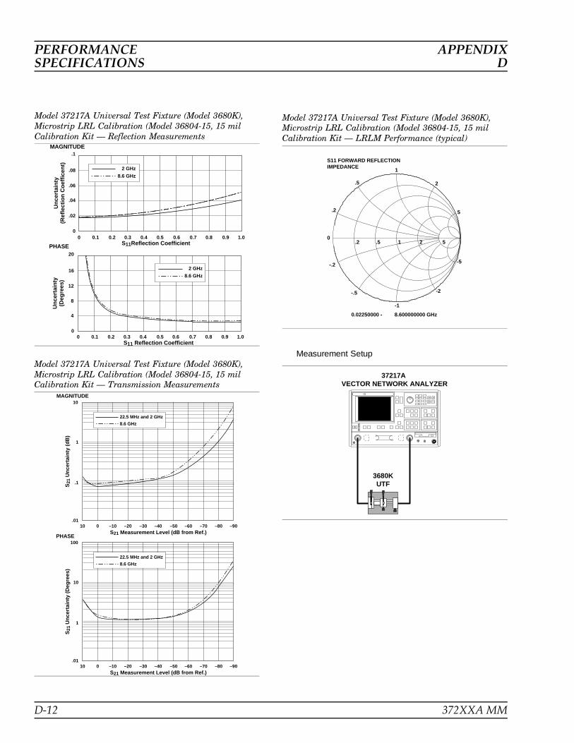
MAGNITUDE
S11Reflection Coefficient0 0.1 0.2 0.3 0.4 0.5 0.6 0.7 0.8 0.9 1.0
2 GHz
8.6 GHz
Unc
erta
inty
(R
efle
ctio
n C
oeffi
cent
)
.1
.08
.06
.04
.02
0
2 GHz
8.6 GHz
Unc
erta
inty
(D
egre
es)
PHASE
S11 Reflection Coefficient0 0.1 0.2 0.3 0.4 0.5 0.6 0.7 0.8 0.9 1.0
4
8
12
16
20
0
Model 37217A Universal Test Fixture (Model 3680K), Microstrip LRL Calibration (Model 36804-15, 15 milCalibration Kit — Reflection Measurements
MAGNITUDE
S21
Unc
erta
inty
(dB
)
S21 Measurement Level (dB from Ref.)
10
1
.1
.0110 0 –10 –20 –30 –40 –60 –70 –80 –90–50
22.5 MHz and 2 GHz
8.6 GHz
S21
Unc
erta
inty
(D
egre
es)
PHASE
S21 Measurement Level (dB from Ref.)
100
10
1
.0110 0 –10 –20 –30 –40 –60 –70 –80 –90–50
22.5 MHz and 2 GHz
8.6 GHz
Model 37217A Universal Test Fixture (Model 3680K), Microstrip LRL Calibration (Model 36804-15, 15 milCalibration Kit — Transmission Measurements
0.02250000 - 8.600000000 GHz
.5
5
2
0
1
-.2
-2
-1
-5
.2
-.5
.2 .5 1 2 5
S11 FORWARD REFLECTION IMPEDANCE
Model 37217A Universal Test Fixture (Model 3680K), Microstrip LRL Calibration (Model 36804-15, 15 milCalibration Kit — LRLM Performance (typical)
37217A VECTOR NETWORK ANALYZER
3680K UTF
Measurement Setup
PERFORMANCE APPENDIXSPECIFICATIONS D
D-12 372XXA MM

MAGNITUDE
Unc
erta
inty
(R
efle
ctio
n C
oeffi
ent)
.05
.04
.03
.02
.01
0
Reflection Coefficient0 0.1 0.2 0.3 0.4 0.5 0.6 0.7 0.8 0.9 1.0
40 MHz and 2 GHz
18 GHz
PHASE
Reflection Coefficient0 0.1 0.2 0.3 0.4 0.5 0.6 0.7 0.8 0.9 1.0
10
8
6
4
2
0
40 MHz and 2 GHz
18 GHz
Unc
erta
inty
(D
egre
es)
Models 37225A and 37247A (GPC-7 Connectors), Reflection Measurements
S21 Measurement Level (dB from Ref.)
40 MHz
2 GHz
18 GHz
MAGNITUDE
S21
Unc
erta
inty
(dB
)
10
1
.1
.0110 0 –10 –20 –30 –40 –60 –70 –80 –90–50
S21 Measurement Level (dB from Ref.)10 0 –10
40 MHz
2 GHz
18 GHz
PHASE
S21
Unc
erta
inty
(D
egre
es)
100
10
1
.01–20 –30 –40 –60 –70 –80 –90–50
Models 37225A and 37247A (GPC-7 Connectors), Transmission Measurements
2 GHz
18 GHz
Unc
erta
inty
(D
egre
es)
PHASE
Reflection Coefficient0 0.1 0.2 0.3 0.4 0.5 0.6 0.7 0.8 0.9 1.0
2
4
6
8
10
0
Unc
erta
inty
(R
efle
ctio
n C
oeffi
cien
t)
MAGNITUDE
.01
.02
.03
.04
.05
0
2 GHz
18 GHz
0 0.1 0.2 0.3 0.4 0.5 0.6 0.7 0.8 0.9 1.0Reflection Coefficient
Models 37225A and 37247A (Type N Connectors), Reflection Measurements
40 MHz
2 GHz
18 GHz
PHASE
S21
Unc
erta
inty
(D
egre
es)
S21 Measurement Level (dB from Ref.)
100
10
1
.0110 0 –10 –20 –30 –40 –60 –70 –80 –90–50
–90
MAGNITUDE
S21
Unc
erta
inty
(dB
)
S21 Measurement Level (dB from Ref.)
10
1
.1
.0110 0 –10 –20 –30 –40 –60 –70 –80–50
40 MHz
2 GHz
18 GHz
Models 37225A and 37247A (Type N Connectors), Transmission Measurements
APPENDIX PERFORMANCED SPECIFICATIONS
372XXA MM D-13

MAGNITUDE
S11Reflection Coefficient0 0.1 0.2 0.3 0.4 0.5 0.6 0.7 0.8 0.9 1.0
40 MHz and 2 GHz
20 GHz
Unc
erta
inty
(R
efle
ctio
n C
oeffi
cent
)
.05
.04
.03
.02
.01
0
40 MHz and 2 GHz
20 GHz
Unc
erta
inty
(D
egre
es)
PHASE
S11 Reflection Coefficient0 0.1 0.2 0.3 0.4 0.5 0.6 0.7 0.8 0.9 1.0
2
4
6
8
10
0
Models 37225A and 37247A (GPC-7 Connectors), Reflection Measurements
MAGNITUDE
S21
Unc
erta
inty
(dB
)
S21 Measurement Level (dB from Ref.)
10
1
.1
.0110 0 –10 –20 –30 –40 –60 –70 –80 –90–50
40 MHz
2 GHz
20 GHz
S21
Unc
erta
inty
(D
egre
es)
PHASE
S21 Measurement Level (dB from Ref.)
100
10
1
.0110 0 –10 –20 –30 –40 –60 –70 –80 –90–50
40 MHz
2 GHz
20 GHz
Models 37225A and 37247A (GPC-7 Connectors), Transmission Measurements
MAGNITUDE
Reflection Coefficient0 0.1 0.2 0.3 0.4 0.5 0.6 0.7 0.8 0.9 1.0
40 MHz and 2 GHz
20 GHz
Unc
erta
inty
(R
efle
ctio
n C
oeffi
cent
)
.05
.04
.03
.02
.01
0
40 MHz and 2 GHz
20 GHz
Unc
erta
inty
(D
egre
es)
PHASE
Reflection Coefficient0 0.1 0.2 0.3 0.4 0.5 0.6 0.7 0.8 0.9 1.0
2
4
6
8
10
0
Models 37225A and 37247A (K Connectors), Reflection Measurements
40 MHz
2 GHz
20 GHz
MAGNITUDE
S21
Unc
erta
inty
(dB
)
S21 Measurement Level (dB from Ref.)
10
1
.1
.0110 0 –10 –20 –30 –40 –60 –70 –80 –90–50
PHASE
S21
Unc
erta
inty
(D
egre
es)
S21 Measurement Level (dB from Ref.)
100
10
1
.0110 0 –10 –20 –30 –40 –60 –70 –80 –90–50
40 MHz
2 GHz
20 GHz
Models 37225A and 37247A (K Connectors), Transmission Measurements
PERFORMANCE APPENDIXSPECIFICATIONS D
D-14 372XXA MM

MAGNITUDE
S11Reflection Coefficient0 0.1 0.2 0.3 0.4 0.5 0.6 0.7 0.8 0.9 1.0
40 MHz and 2 GHz
20 GHz
40 GHz
Unc
erta
inty
(R
efle
ctio
n C
oeffi
cent
)
.05
.04
.03
.02
.01
0
40 MHz and 2 GHz
20 GHz
40 GHz
Unc
erta
inty
(D
egre
es)
PHASE
S11 Reflection Coefficient0 0.1 0.2 0.3 0.4 0.5 0.6 0.7 0.8 0.9 1.0
2
4
6
8
10
0
Model 37269A (K Connectors), Reflection Measurements
MAGNITUDE
S21
Unc
erta
inty
(dB
)
S21 Measurement Level (dB from Ref.)
10
1
.1
.0110 0 –10 –20 –30 –40 –60 –70 –80 –90–50
40 MHz
2 GHz
20 GHz
40 GHz
PHASE
S21
Unc
erta
inty
(D
egre
es)
S21 Measurement Level (dB from Ref.)
100
10
1
.0110 0 –10 –20 –30 –40 –60 –70 –80 –90–50
40 MHz
1 GHz
20 GHz
40 GHz
Model 37269A (K Connectors), Transmission Measurements
MAGNITUDE
S11Reflection Coefficient0 0.1 0.2 0.3 0.4 0.5 0.6 0.7 0.8 0.9 1.0
2 GHz
20 GHz
40 GHz
Unc
erta
inty
(R
efle
ctio
n C
oeffi
cent
)
.1
.08
.06
.04
.02
0
2 GHz
20 GHz
40 GHz
Unc
erta
inty
(D
egre
es)
PHASE
S11 Reflection Coefficient0 0.1 0.2 0.3 0.4 0.5 0.6 0.7 0.8 0.9 1.0
4
8
12
16
20
0
Model 37269A Universal Test Fixture (Model 3680K), Microstrip LRL Calibration (Model 36804-10, 10 milCalibration Kit — Reflection Measurements
PHASE
S21
Unc
erta
inty
(D
egre
es)
S21 Measurement Level (dB from Ref.)
100
10
1
.0110 0 –10 –20 –30 –40 –60 –70 –80 –90–50
MAGNITUDE
S21
Unc
erta
inty
(dB
)
S21 Measurement Level (dB from Ref.)
10
1
.1
.0110 0 –10 –20 –30 –40 –60 –70 –80 –90–50
2 GHz
20 GHz
40 GHz
2 GHz
20 GHz
40 GHz
Model 37269A Universal Test Fixture (Model 3680K), Microstrip LRL Calibration (Model 36804-10, 10 milCalibration Kit — Transmission Measurements
APPENDIX PERFORMANCED SPECIFICATIONS
372XXA MM D-15

.5
5
2
0
1
-.2
-2
-1
-5
.2
-.5
0.04000000 - 40.000000000 GHz
.2 .5 1 2 5
S11 FORWARD REFLECTION IMPEDANCE
Model 37269A Universal Test Fixture (Model 3680K), Microstrip LRL Calibration (Model 36804-10, 10 milCalibration Kit — LRLM Performance (typical) 37269A
VECTOR NETWORK ANALYZER
3680K UTF
Measurement Setup
PERFORMANCE APPENDIXSPECIFICATIONS D
D-16 372XXA MM

Appendix EPerformance VerificationSoftware User’s Guide
This appendix contains the Model 360X/372XXA Vec-tor Network Analyzer Performance VerificationSoftware User’s Guide. This user’s guide providestechnical data and procedures that can aid you inperforming maintenance on the 372XXA.

490 JARVIS DRIVEMORGAN HILL, CA 95037-2809
P/N: 10410-00162REVISION:A
PRINTED: FEBRUARY 1995COPYRIGHT 1995 WILTRON CO.
Model 360X/372XXAVector Network Analyzer
Performance Verification Software
Software User’s Guide
Software Revision 1.03
This manual applies to the WILTRON 360X/372XXA Vector Network Analyzer
Performance Verification Software, WILTRON Part Number 2300-175, Revision 1.03

WARRANTY
The WILTRON product(s) listed on the title page is (are) warranted against defectsin materials and workmanship for one year from the date of shipment.WILTRON’s obligation covers repairing or replacing products which prove to bedefective during the warranty period. Buyers shall prepay transportation chargesfor equipment returned to WILTRON for warranty repairs. Obligation is limited tothe original purchaser. WILTRON is not liable for consequential damages.
LIMITATION OF WARRANTY
The foregoing warranty does not apply to WILTRON connectors that have faileddue to normal wear. Also, the warranty does not apply to defects resulting fromimproper or inadequate maintenance by the Buyer, unauthorized modification ormisuse, or operation outside of the environmental specifications of the product. Noother warranty is expressed or implied, and the remedies provided herein are theBuyer’s sole and exclusive remedies.
TRADEMARK ACKNOWLEDGEMENTS
V Connector and K Connector are registered trademarks of WILTRON Company.Ink Jet and Think Jet are registered trademarks of Hewlett-Packard Co.MS-DOS is a registered trademark of Microsoft Corporation.
NOTICE
WILTRON Company has prepared this manual for use by WILTRON Companypersonnel and customers as a guide for the proper installation, operation andmaintenance of WILTRON Company equipment and computer programs. The draw-ings, specifications, and information contained herein are the property of WILTRONCompany, and any unauthorized use or disclosure of these drawings, specifications,and information is prohibited; they shall not be reproduced, copied, or used in wholeor in part as the basis for manufacture or sale of the equipment or softwareprograms without the prior written consent of WILTRON Company.

i/ii
Table of Contents
Chapter 1 General Information
1 Introduction . . . . . . . . . . . . . . . . . . . . 12 Format of the Verification Software Disks . . . . 13 Capability . . . . . . . . . . . . . . . . . . . . . 14 Data Output . . . . . . . . . . . . . . . . . . . . 1
Chapter 2 Required Equipment
5 Introduction . . . . . . . . . . . . . . . . . . . . 36 Computer (System Controller) . . . . . . . . . . 37 GPIB Interface Card . . . . . . . . . . . . . . . 38 Vector Network Analyzer . . . . . . . . . . . . . 39 Verification Kit . . . . . . . . . . . . . . . . . . 310 Printer . . . . . . . . . . . . . . . . . . . . . . . 411 Cables . . . . . . . . . . . . . . . . . . . . . . . 4
Chapter 3 Configuring the System
12 Introduction . . . . . . . . . . . . . . . . . . . . 513 Hardware Interconnection . . . . . . . . . . . . 514 Performance Verification
(PV) Software Installation . . . . . . . . . . . 5
Chapter 4 Running the Program
15 Introduction . . . . . . . . . . . . . . . . . . . . 616 Starting the Program . . . . . . . . . . . . . . . 617 Entering System Data and Calibration . . . . . 718 Measuring the Verification Devices . . . . . . . 8
Chapter 5 In Case of Trouble
19 Difficulty Running the Program . . . . . . . . . 1020 Difficulty Meeting System Specifications . . . . 10

Chapter 1General Information
Contents Para Name Page
1 Introduction . . . . . . . . . . . . . . . . . . . . . . . . . . . . 12 Format Of The Verification Software Disks . . . . . . . . . . 13 Capability . . . . . . . . . . . . . . . . . . . . . . . . . . . . . 14 Data Output . . . . . . . . . . . . . . . . . . . . . . . . . . . 1
1 Introduction
This manual supports the WILTRON 2300-175 VNA Performance Veri-fication Software. This software is used with the WILTRON360X/372XXA Vector Network Analyzer Systems. The manual is organ-ized into five chapters, as shown below.
• General Information—provides an overview of the product.
• Required Equipment—describes the test equipment, compo-nents, hardware and software required to use this product.
• Configuring the System—describes how the equipment is setupand interconnected.
• Running the Program—provides step-by-step instructions forrunning the software.
• In Case of Trouble—contains troubleshooting suggestions andservice information.
2 Format of the Verification Software Disks
The Performance Verification Software is offered on an IBM compatible720KB floppy disk.
3 Capability
This software provides for automating measurements of the test com-ponents contained in a WILTRON 3666, 3667, 3668, 3669, or 3669BVerification Kit.
It compares the measurements made on your 360X/372XXA with thetest component data provided in each verification kit. This will aid indetermining if the measurement values obtained for the componentsare within the uncertainty limits provided on the data disk packagedwith each verification kit.
4 Data Output
The test data and results are output in the form of four files to the rootdirectory of your computer’s drive C:\ (in the root directory.) Thedefault file names are:
Page 1

20db_pad.dat
40db_pad.dat (or 50db_pad.dat)
air_line.dat
rho__std.dat
NOTE:
The Performance Verification Software allows you to renamethese files to file names of your choice with default “.dat”extension.
The tabular data in each file is given at discrete frequencies (1.0, 1.5,or 3.0 GHz intervals—depending on the connector type and correspond-ing frequency range).
Page 2

Chapter 2Required Equipment
Contents Para Name Page
5 Introduction . . . . . . . . . . . . . . . . . . . . . . . . . . . . 3 6 Computer (System Controller) . . . . . . . . . . . . . . . . . 3 7 GPIB Interface Card . . . . . . . . . . . . . . . . . . . . . . . 3 8 Vector Network Analyzer . . . . . . . . . . . . . . . . . . . . 3 9 Verification Kit . . . . . . . . . . . . . . . . . . . . . . . . . . 310 Printer . . . . . . . . . . . . . . . . . . . . . . . . . . . . . . 311 Cables . . . . . . . . . . . . . . . . . . . . . . . . . . . . . . . 4
5 Introduction
This section describes the equipment required to use the PerformanceVerification Software.
6 Computer (System Controller)
You need an IBM AT or compatible computer with 640K of RAM, a harddisk configured as C: drive, a 3.5 inch floppy disk drive, and MS-DOS3.3 (or higher) Operating System. This computer system is also usedas the system controller (see below for GPIB configuration.)
7 GPIB Interface Card
Your computer must have a National Instruments IEEE-488 GPIBInterface Adapter running driver version 2.1 or later. Ensure yourGPIB adapter is setup to default configuration as per National’s In-structions.
8 Vector Network Analyzer
You need a WILTRON Model 360X/372XXA Vector Network AnalyzerSystem, with the appropriate 3650, 3651, 3652, 3654, or 3654B Cali-bration Kit. A 360X system consists of a 360/360A/360B VNA, a 36XX-Series Test Set, and a Wiltron RF signal source.
The 360X/372XXA Vector Network Analyzer will be referred to as VNAthroughtout this User’s Guide.
9 Verification Kit
You need a WILTRON 3666, 3667, 3668, 3669, or 3669B Verification Kit,with data disk.
Page 3

10 Printer
A printer is not required since the verification results and data will bestored in four files on your computer’s hard disk drive (C:). These filesare saved in ASCII format for easy viewing and printing later if de-sired.
11 Cables
You need a GPIB cable (Wiltron PN: 2100-2) and a two-foot RF TestPort Cable (WILTRON PN: 3670A50-2, 3670K50-2, 3670V50-2,3671A50-2, 3671K50-2, or 3671V50-2.)
Page 4

Chapter 3Configuring the System
Contents Para Name Page
12 Introduction . . . . . . . . . . . . . . . . . . . . . . . . . . . . 513 Hardware Interconnection . . . . . . . . . . . . . . . . . . . . 514 Software Installation and Configuration . . . . . . . . . . . . 5
12 Introduction
This chapter describes how the various system elements are intercon-nected and the preliminary steps required for operation of the verifi-cation software.
13 Hardware Interconnection
Connect the computer’s GPIB port to the VNA system using the GPIBcable.
If the VNA is a 360X Network Analyzer, connect to the GPIB connecterlabeled “360 GPIB” not the one labeled “System Bus.”
If the VNA is a 372XXA Network Analyzer, connect to the GPIB con-necter labeled “IEEE 488.2 GPIB” not the one labeled “DedicatedGPIB.”
Connect the two-foot test port cable female end to the VNA Port 2.
Connect a female-female Phase Equal Instertable Adapter from theCalibration Kit to the VNA Port 1. This does not apply to GPC-7Calibration.
14 Performance Verification (PV) Software Installation
The PV software can either be run directly from the floppy disk orcopied to and run from your C: drive. The Verification data disk, whenrequested by the PV software must be installed in drive A:.
NOTE:
The PV distribution disk contains batch files that show ex-amples of how to set up your computer so that B: drive canbe used.
Ensure your GPIB Adapter driver software is installed and tested asper National Instrument’s Instructions.
Page 5

Chapter 4Running the Program
Contents Para Name Page
15 Introduction . . . . . . . . . . . . . . . . . . . . . . . . . . . . 616 Starting The Program . . . . . . . . . . . . . . . . . . . . . . 617 Entering System Data And Calibration . . . . . . . . . . . . . 718 Measuring the Verification Devices . . . . . . . . . . . . . . . 8
15 Introduction
The Performance Verification software runs in DOS text mode as de-scribed below.
16 Starting the Program
With the equipment and software configured as described in Chapter 3,turn your computer on and allow it to boot up to the DOS prompt (C:\.)
Once the computer has finished booting up to the DOS prompt, insertthe performance verification software disk in drive A: or start it fromyour C: drive.
At the DOS prompt, Type:
vnaveri
Press: <ENTER> to invoke the performance verification program.
The following message will be displayed on the computer screen:
WILTRON VNA VERIFICATION SOFTWARE
* * VERSION 1.03 * *
Press any key to continue.
At this point you can install the 3.5-inch data disk from the VerificationKit into drive A: and leave it in for the duration of the PerformanceVerification.
Page 6

17 Entering System Data and Calibration
The program now prompts you to enter the following data:
• Start Frequency
• Verification Kit Type
• Stop Frequency
Enter the information as it is requested.
Next, you will be prompted to verify that the calibration kit coefficientshave been loaded into the VNA system. To do this:
a. Insert the data disk from your WILTRON Calibration Kit (not theverification kit) in the Network Analyzer’s disk drive.
b. Press the UTILITY MENU key on the front panel of the networkanalyzer. (The Utility Menu is displayed on the network analyzer’sdisplay screen.)
c. Select CALIBRATION COMPONENT UTILITIES on the UtilityMenu and press <ENTER>. (The Calibration Component UtilitiesMenu is displayed.)
d. Select INSTALL CALIBRATION COMPONENT INFORMATIONFROM DISK on the Calibration Component Utility Menu andpress <ENTER>. (Loading of the calibration kit coefficients fromthe data disk begins.)
When the calibration kit coefficients have been loaded into the VNAsystem, press any key on the computer keyboard to continue.
The program automatically sets up the proper frequency points foryour measurement based upon your responses to the earlier programprompts. The program then automatically sets up the VNA so that youcan manually perform a full, 12-term calibration of the VNA system.Using the two-foot test cable, set up the VNA system for calibration asshown in Figure 1. Perform the full, 12-term calibration following theprompts presented on the network analyzer’s display screen and usingthe calibration components from your WILTRON Calibration Kit.
Completion of the calibration is indicated by the lighting of the “FULL12-TERM” CALIBRATION LED indicator on the 360X VNA and the“APPLY CAL” LED indicator only on the 372XXA VNA front panel.
Press any key on the computer keyboard to continue the verificationprogram.
Next, the program prompts you to enter header information for thedata printouts, as follows:
• VNA Serial Number (found on the Network Analyzer’s rearpanel).
• Verification Kit Serial Number (found on the label on the side ofthe verification kit wooden box).
• Date (dd/MONTH/yy format). For example, if the date is Sep-tember 1, 1993 then enter 01/SEPT/93 .
• Operator’s Name (up to 12 characters long-no spaces).
Page 7

Enter the information as it is requested, pressing <ENTER> after eachentry.
The program now prompts you to verify that the Verification Kit datadisk is installed in drive A: of your computer. Install the disk if youhave not already done so.
18 Measuring the Verification Devices
The program now presents the following menu on the computer screen:
(1) Measure 20 dB Attenuator(2) Measure 40 or 50 dB Attenuator(3) Measure Beatty Standard(4) Measure Airline(5) Exit
Enter the number corresponding to the action you wish to take.
At this point you can begin measuring your verification kit devices. Asyou select a verification device, the program prompts you to enter theserial number of the device and to orient the device with the labelfacing the user. Such orientation places port 1 on your left. It is at thismeasurement point that the device is installed and measured on theVNA. See Figure below showing the measurement setup.
The computer will now read data from the Verification Kit data disk(installed in drive A:.) The verification software then automaticallymeasures the device with the VNA and compares the measured datawith the data stored on the Verification Kit data disk. The results andmeasurement data is stored to data files on your C: hard drive (seeSection 1-4, Data Output for file names.) The data on each file will
NETWORKANALYZER
SIGNALSOURCE
TEST SET
2 FOOTTEST CABLE
INSERTCALIBRATION
COMPONENTSHERE
PORT 1 PORT 2
Figure 1. VNA Calibration and Measurement Setup Shown on a 360X VNA.
Page 8

contain an asterisk (*) next to measrement data that is not within thespecified limits.
The above steps can be repeated for each of the three remaining devicesin the verification kit: the 40/50 dB attenuator, the Beatty standard,and the air line.
NOTE:
The software will write the data to the file name you choose,or the default file names in Section 1-4. If these files alreadyexist, they will be overwritten. Rename the files if you donot wish them overwritten with the new data.
To exit the program, enter 5 at the main menu.
To view or print the data files, simply use any text editor. You can alsoview the data files using the batch file called veridata.bat included onyour Performance Verification Software distribution disk.
Page 9

Chapter 5In Case of Trouble
Contents Para Name Page
19 Difficulty Running the Program . . . . . . . . . . . . . . . . 1020 Difficulty Meeting System Specifications . . . . . . . . . . . 10
19 Difficulty Running the Program
If you have difficulty getting the program to run properly:
a. Check your GPIB interconnection.
b. Check cables and addresses, ensure that the GPIB-PC directory ispresent on the boot drive and contains the GPIB.COM file, and thatthe CONFIG.SYS file contains the line DEVICE=GPIB.COM.
c. Ensure that the performance verification software disk is in driveA: and that it contains the VNAVERI.EXE file.
d. Ensure that after starting-up your Perfomance Verification Soft-ware, the Verification Kit data disk is installed in drive A: and thatit contains the following files:
DEV1S11.DAT DEV3S11.DAT UNCDEV1.DATDEV1S12.DAT DEV3S12.DAT UNCDEV2.DATDEV1S21.DAT DEV3S21.DAT UNCDEV3.DATDEV1S22.DAT DEV3S22.DAT UNCDEV4.DATDEV2S11.DAT DEV4S11.DAT VALDEV1.DATDEV2S12.DAT DEV4S12.DAT VALDEV2.DATDEV2S21.DAT DEV4S21.DAT VALDEV3.DATDEV2S22.DAT DEV4S22.DAT VALDEV4.DAT
e. Ensure ANSI.SYS is a device in your CONFIG.SYS file. For exam-ple, if your Disk Operating System is in a directory called DOS onyour C drive, you would add the following line to your CONFIG.SYSfile: DEVICE = C:\DOS\ANSI.SYS.
If, after checking the above, you still have difficulty, contact WILTRONCustomer Service at (408) 778-2000 (fax: 408 778 0239) and ask for theVector Network Analyzers Support Engineer for further assistance.
20 Difficulty Meeting System Specifications
If the verification software appears to run properly but the results arenot within the measurement limits associated with the verification kit:
a. Check both the verification kit and calibration kit devices for signsof physical damage. Make sure that the connectors are clean.
b. Ensure that the serial number of the verification kit data diskmatches that shown on the verification kit.
Page 10

c. Repeat the process with a fresh calibration. Save the results of bothmeasurements as an aid in troubleshooting, if you require factoryassistance.
d. When installing calibration devices, and when measuringverification devices, pay particular attention to proper connectoralignment and torque. Torque the connector using the torquewrench supplied with the calibration kit.
If, after following the above steps, you still have difficulty, pleasecontact WILTRON Customer Service at (408) 778-2000 (fax: 408 7780239) and ask for the Vector Network Analyzers Support Engineer forfurther assistance.
Page 11/Page 12

Appendix AExample of Tabular Test Results
WILTRON VNA Verification SW Version 1.03
37200 Serial Number: 456001
Verification Kit Model Number: 3667
Verification Kit Serial Number: 89001
Date: 15/JAN/95
Device Serial Number: 050021
Operator: John
20 DB ATTENUATOR
—————————————————-S12—————————————————-
Freq(GHz)
STD(db)
MEAS(db)
DIFF UNC(+/-)
STD(DEG)
MEAS(DEG)
DIFF UNC(+/-)
0.02 -19.92 -19.90 -0.02 0.41 -3.6 -2.3 -1.3 5.2
1.00 -19.95 -19.92 -0.03 0.14 - 85.8 -85.9 0.1 1.1
2.00 -19.97 -19.93 -0.04 0.14 -171.5 -171.5 0.0 1.2
3.00 -19.99 -19.95 -0.04 0.14 -102.9 -102.9 0.0 1.3
Appendix A A1