model 92 computer theory of operation manual (preliminary)€¦ · · 2010-06-10model 92 computer...
TRANSCRIPT

MODEL 92 COMPUTER THEORY OF OPERATION
MANUAL (PRELIMINARY)
SDS 900864A June 1965

MODEL 92 COMPUTER THEORY OF OPERATION
MANUAL (PRELIMINARY)
SDS 900864A June 1965
~jji-·L~
SCIENTIFIC DATA SYSTEMS/1649 Seventeenth Street/Santa Monica, California/UP 1-0960
@1965 Scientific Dato Systems, Inc. Printed in U.S.A.

Chapter 1
. Chapter 2 ..
Chapter 3
Chapter 4
Chapter 5
~hapter 6
CONTENTS
Introduction to the Hardware
1. 1 . Hardware Characteristics
f.2· Hardware Organization
Introduction to Programming
2. 1 Memory Word Format
2 .. 2 Instruction Word Format
2 .. 3 Operand Word Format
2. 4 De scription of Opcode s
2.5 Memory Allocation
Timing
3. 1 Common Clock
3.2 Clock ~ounte r
3.3 Phases
3.4 Cycle Alteration
3.5 Summary
Memory
4. 1 Basic Operation
4.2 Parity
4. 3 Timeshare
Adder
5. 1 Introduction
5.2 Operations
Basic Internal Operations
6. 1
6.2
6. 3
604
6.5
Introduction to Timing Charts
End
Operand Assembly
Trap
Basic Opcodes
i
Page
1-2
1-3
2-1
2-1
2-5
2-5
2 -12
3 -1
3-1
3-1
3-1
3-2
4-1
4-2
4-4
5-1
5-2
6-1
6-1
6-13
6-15

Chapter 7
Chapter 8
Chapter 9
CONTENTS (Continued)
Console Operations
7. 1
7.2
7. 3
7.4
7.5
7. 6
Introduction
Register Display/Alteration
Console Functions
Fill
Miscellaneou.s Switches
Lights
Interrupts
8. 1
8.2
8. 3
8. 4
8.5
Introduction
Recognition
BRC Opcode
Leaving Idle
Single Instruction Interrupts
Alert and Text r/o EquipITlent
9. 1
9. 2
9. 3
Introdu ction
EOM Opcode
SES Opcode
Page
7-2
7-4
7-7
7-14
7 -17
7-19
8-1
8-4
"8-6
8-8
8-10
9-1
9-3
9-7
Chapter 10 Parallel I/O
10. 1 Introdu ction
, 10.2 Connectors
10. 3 POT /BPO Opcode s
10.4 PIN/BPIOpcodes
Chapter 11 Standard r/o Channel
10-1
10-4
10-6
10-10
11. 1 Initialization 11-1
11. 2 Character TransITlission and Precessing 11-1
11. 3 Parity 11-5
11. 4 Channel Error 11-5
ii

CONTENTS (Continued)
Page
Chapter 11 Standard I/O Channel (Continued)
11.5 . Te rmination 11-6
11.6 Channel Te sts 11-8
11. 7 Interrupts 11-9
11. 8 Mag-tape Scan 11-9
11. 9 Interlace 11-10
11. 10 Connectors 11-12
II. 11 Channel Timing Charts 11-14
11. 12 Channel Opcode s 11-38
11. 13 WOT fROT Opcodes 11-39
11. 14 WINfRIN Opcodes 11-41
iii

PREFACE
Model 92 Computer is a high-speed, general purpo.se
digital computer designed for real-time systems
control, dire ct digital control, message switching,
and repetitive, high-speed computation. The computer
is completely modu.1ar, u.tilizing monolithic integrated
c.ircuits!.
This p~elimin~ry m·anual des'cribes the hardware logic
and opeloation of the central processor, memory, and
control console. Additional information on programming,
logic, and circuits can be found in the following
pUblications:
SDS 900505B
SDS 900925A
SDS 900921A
SDS 900922A
SDS 92 Computer Reference Manual
Model 92 Computer Logic Equations,
Main Frame and Memory
Mode192 Computer General Reference
Drawings
92 Computer Mod'~~de Reference Data

Model 92 Computer

CHAPTER 1
Introduction to the Hardware
1. 1 Hardware characteristics
1.2 Hardware organization
...... I
......
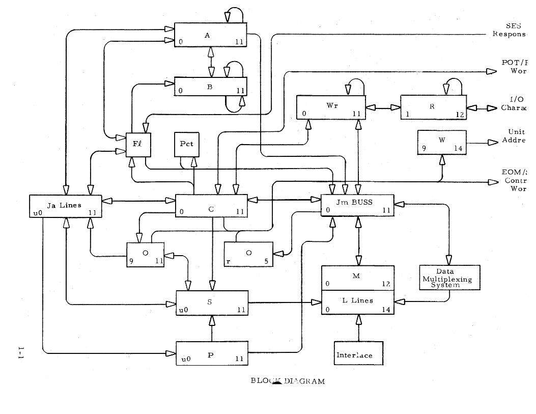
uO Ja Lines
11
9
Pct
0
a
uO
uO
0
C 11
o r 5
S 11
P 11
BLOl~DI.i\Gl\AM
~r
11 1
0 11
M 0 I?
L Lines 0 14
Inter:ace
SES Respons,
POTIF ----~------~C> ~or
1/0 R Charac
12
Unit ~ Addre
9 14
EOM/~ Contr ~or
Data Mu)tiplexing
Syste-m

1. 1 Hardware characteristics
All flip-flops used in the 92 main frame have the following hardware
characteristics:
1. All flip-flops are the usual RS type. However, they also
'receive a common clock. , All changes of state are made
'on the falling edge of this clock., [This means that the
contents of two 'flip..;flopsmay be directlY'interchanged;
e. g.
sAl
rAl
sBl
rBl
= =
=
=
Axb El
Axb 131
Axb Al
Axb .AT
When the gating term Axb is true, th~ falling edge of the
cl()ck will swap A I and B 1. ]
2. If the set term and the reset term'are both true, the flip
flop will se t on the falling edge of the clock. [This means
the example above may be simplified to:
sAl
rAI
sBI
,rBl
=
=
Axb BI
Axb
A,xb Al
Axb]
Loglcally, any flip-flop in the 92 main frame falls into one of two groups:
1. Standard RS type. These are recognizable 'in the equations as
those flip-flops which have both a SET equation and a RESET
equation; e. g. ,
1-2

sAl
rAl
=
=
Axb El
Axb
2. Repeate'r type. These flip-flops will automatically reset
if there is no set input~ However, ·these flip-flops will
not set or reset unless they receive an enable signal.
[This is accomplished by holding the reset true and
using the enable to gate the common clock.] These flip
flops are recognizable in the equations as those which
have a SET equation (only) and an ENABLE equation; e. g. ,
sB 1 = Al
Eg = Axb
Most of the logi'c is implemented via AND-OR -BUFFER or AND-OR
INVER TER hardware. The outstanding exceptions are the terms which
enable the proper inputs to the adder. The se have been implemented
viaNANDS because of speed considerations.
1. 2 Hardware organization
A REGISTER
FUNCTION:
. The A register is the index register. A also defines the block
length for block I/O opcodes (50,51,54·,55). A may also be used
as an auxill·ary accum.ulator.
IMPLEMENT ATION:
12 repeate r flip .. flop s de signate d A 0, ... , AIL
CONTROL TERMS:
Ag enahles the repeater flip-flops that make up A
1-3

Axas
Axb
Axja
Axjas
B REGISTER
FUNCTION:
shifts A left one binary bit position
interchanges A and B
gates Ja into A
gates Ja, shifted right one binary bit position,
into A
The P. register is the main accumulator.
IMPLENIENTA TION:
12 repeater flip-flops designated BO, ••• , B 11.
CONTROL TERMS:
Bg enables the repeater flip-flops that make up B
Axb
Axjas -
Bxbs,.l -
interchanges B and A
shifts B right one binary bit position
shifts B left one binary bit position
C REGISTER
FUNCTION:
The C register acts as the main exchange register
between memory (M) and both the internal logic and the input/
output logic.
IMPLEMENTATION:
12 repeater flip;..flops designated CO, • •• , C 11.
CONTROL TERMS:
Cg enables the repeater flip-flops that make up C
1-4

FJ...
Cx!
Cxja
Cxjm
Cxw
FUNCTION:
gates a PIN input word into C
gates Ja into C
gates Jm into C
gates Wr into C
F.l: holds arithmetic overflow information. Fl also holds the
re suIt (0 or 1) of a sense or compare instru ction.
IMPLEMENTATION:
1 RS flip-flop designated FJ. However, the implementation is
such that Fl appears to be a repeater flip-flop.
CONTROL. TERMS:
F): g enable s the quasi-repeater flip -flop F:'f..
is the set signal to the quasi-repeater flip-flop Fe.
Ja LINES
FUNCTION:
The Ja LINES are the outputs of the adder.
IMPLEMENTATION:·
15 lines designated JauO, Jau1, Jau2, JaO, •.. , JaIl.
CONTROL TERMS:
Gpxa
Gpxad
Gpxam
Gpxc
gates A ohto Ja
gates A + C onto Ja
gate sA ... 1 on to J a
gates C or C + 1 onto Ja
1-5
Gpxeo
Gpxex
Gpxs
Gpxsi
Gpxsu
Gnnac
Prbu
Jm EUSS
FUNCTION=
gates A (±) C onto Ja
gates A /\ C onto Ja
gates S onto Ja
gates S + 1 onto Ja
gates A -C onto Ja
gates C-A onto Ja
m.erges the control panel SET BUTTONS with the
current contents of Ja
The Jm BUSS is the m.em.ory buss.
IMPLEMENTATION:
12 line s de signated Jm.O, ... , Jm 11.
CONTROL TERMS:
gates A onto Jm.
gates C onto Jm.
gates PO-PI 1 onto Jm
gate s [F),.Pct, 0, .... ,0, PuO ,Pu 1, Pu2] onto Jm..
gates Wr onto Jm.
gates M onto Jm
Jmxa
Jm.xc
Jm.xp
Jm.xpu
Jmxwr
Mw
Jm.xz gates the Data Multiplexing System.s input word onto Jm
L LINES
FUNCTION:
The L LINES contain the address of. the current memory re£erente ..
1-6

IMPLEMENTATION:
151inesdesignated LO, •.• ,.L14.
CONTROL TERMS:
Ts gates S onto L
Ts Dmc .. gates the interlace's memory reference address
onto L
Dmc gate s the Data Multiplexing System t s memor y
reference addre s s onto L
M REGISTER
FUNCTION:
The M register holds the contents of (read) or for (write)
thecurreritlyreferenced memory location .
. IMPLEMENT A TION:
13 flip-flops designated MO, ••. ,MI2.
MI2 is the parity bit.
CONTROL TERMS:
Mw
o REGISTER
FUNCTION:
gates Jm to MO through MIl and even parity to MI2.
The 0 register holds the currentopcode.
·IMPLEMENTA TION:
6 repeater flip-flops designated Or, 01, ... , 05.
1-7

CONTROL TERMS:
Og enables the repeater flip-flops that make u-p 0
Tp End
09,010,011
FUNCTION:
gate s the next opcode into 0
09-011 provide temporary storage for the most significant
three bits of a 15-bit operand address. 09-011 also hold part
of an EOM/SES control word.
IMPLEMENTATION:
3 RS flip-flops designated 09, 010, OIl.
CONTROL TEBMS:
eli> Tp Lp - gates SuO-Su2 into 09-011.
<ji) Tp Lp - gates C9-Cll into 09-011.
P REGISTER
FUNCTION:
The P register holds the address of the next instruction.
IMPLEMENT ATION:
15 repeater flip-flops designated PuO, Pul, Pu2, POt ..•• Pl.!.
CONTt{OL TERMS:
Pg
Pxbu
Pxja
Pxp
enables the repeater flip-flops that make up P
gates the control panel set buttons into P
gates Ja into P
recirculates P
1-8

Pct
FUNCTION:
Pct gates the normal execution of the full-word rIo opcodes .
(10/50, 11/51, 14/54, IS/55). PcT causes these commands
to trap.
IMPLEMENT A TION:
1 RS flip -flop de signated Pet.
R REGISTER
FUNCTION:
The R register receives/presents the input/output character
from/to the connected perip~eraL
IMPLEM.ENTATION:
12 repeater flip-flops designated Rl, ... ,RI2.
CONTROL TERMS:
Rg enables the repeater flip-flops that m.ake up R
W4 W9 - gates the output precessing (i. e.intershifting) of R
and Wr
-W4 W9 - gates the input precessing (i. e. intershifting) of R
and Wr
W5 W6 W9 gates the merging of an input character into R
. S REGISTER
FUNCTION:
The S register holds the address of the current memory reference
by the main frame.
1-9

IMPLEMENTATION:
15 repeater flip-flops designated SuO, SuI, Su2, SO, ..• ,811.
CONTROL TERMS
Sg enable s the repeater flip -flops that make up S
Sxci gates C7-Cll into S7-S11
Sxcm
Sxcs
Sxja
Sxp
Int
Tr
W REGISTER
FUNCTION:
gates 09-011 into SuO-Su2 and CO-C6 into SO-S6
gate s 1 into 87 and C9 -C 11 into S8 -S 1 0
gate s Ja into S
gates Pinto S
gates the proper interrupt address into 8 (S2-S10)
gates the proper trap address into S (S5-S10)
The W register holds the unit address of the currently connected
peripheral.
IMPLEMENTATION:
5 repeater flip-flops designated W9, W11, ... , W14
1 RS flip -flop designated WI 0
CONTROL TERMS:
Wg enables the repeater flip-flops that make up W
Wc
Ws
T1 Ta Wh
clears W
gates C6-C 11 into W
clears W
1-10

Wr REGISTER
FUNCTION:
The Wr register provides a one-computer ... wordbuffer betw~en . ,
the main frame logic (C) and .the input/output character (R).·
IMPL'EMENTATION:
12 ·repeater flip-flops designated WrO, .•• , Wr 11.
CONTROL TERMS:
"Wrg
rwWx -
W4
Wrxjm ..
enables the repeater flip-flops that make up Wi:.
gates C into Wr
gates the precessing (i. e. intershifting) of Wr and R
ga~e s Jm into V!r
1-11

CHAPTER 2
Introduction to Programming
2. 1 Memor y word format
2. 2 Instruction word formats
2.3 Operand word format
2.4 Description of opcodes
2. 5 Memor y allocation

2. 1 Menloryword format
The 92 cOnlputer word is 12 binary bits long.
o 1 2 3 4 5 6 7 8 9 10 11
The bi ts will be nun1bered fran!. left to right as shown above.
2. 2 Instruction word formats
The 92 allows 6 different modes of addressing. Some of these modes
need only one computer word to define both the opcode and either the
effective address (i. e. the address of the operand) or the indirect
address (i. e. the address at which addressing is reinitiated). The
remaining addressing modes require two contiguous computer words
to define both th~ opco4e and a co·mputer address.
Addressing Type: Immediate
Instruction Length: One Word
Addressing Area: Next Location
Location Computer Word ........... _ .•. _----- .... _-_ .... __ .. __ ... _._--,
L --- Opcode -_ .. _ ... _,. L_ ......... __ .... _._ ...... -t ..... _-............... _-_.- ... ..
o 1 2 345
L + 1
L+2 Next Instruction
1
6
o 0 0 0 01 ..-........ \ .- -...... ""'" .. _ ...... _ .. _.-'
7 8 9 10 11
Comments: This addressing mode should not be used with the following
opcodes
EXU
BMC
BRM 2-1

Addressing Type: Direct Scratch Pad
Instruction Length: One Word
Addressing Area: Scratch Pad (000018
-000378
)
Location Computer Word
L [: =Opc~de --1 S S S S sl , f I 0 1 2 3 4 5 6 7 8 9 10 11
L+l N ext Ins tru ction
Comments: The operand is taken from location
.000.oOOOOOOS88882
where
888SS 1= 00000
Addressing Type: Full Direct
Instruction Length: Two Words
Addressing Area: Full Memory
Location Computer Word
L ~--Op,code ':: ~ 0 ~+y Y yl 0 1 2 3 4 5 6 7 8 9 10 11
L + 1 I,",,--x_x_x-,+-; X_X,_X-+l_X X ~-t ~=~:X ~ XJ o 1 2 3 4 5 6 7 8 9 10 11
L + 2 Next Instruction
Comments: The operand is taken {r'oTn ideation
YYYXxxxxxxxxxxx 2
2-2

Addressing Type: . Index
Instruction Length: Two Words
Addressing Area: Full Mem.ory
Location Computer Word
L (- O~co~~_ ~'j~_~ ,y y yJ
o 1 2 3 4 5 6 7 8 9 10 11
L + 1 ~ XX X~ :.i""X ~ X X xl ~ i . tl . o 1 2 3 4 5 6 7 8 9 10 11
L + 2 Next Instruction
Comments: The operand is taken from. location
EEEEEEEEEEEEEEE2
where
yyy XXX XXX XXX XXX2
-000 AAA A.AA AAA AAA2
EEE EEE EEE EEE EEE2
and the contents of the A register is given by
AAA AAAAAA AAA 2
Addressing Type: Full Indirect
Instruction Length: Two Words
Addressing Area: Full Memory
2-3

Location Computer Word
L
L + 1
o 1 2 3 4 5 6 7 8 9 10 11
L + 2 Next Instruction
Gom.m.ents: The opcode, as given in location L, is saved; but
addressing is reinitiated at location
Y Y YXXXXXXXXXXXX 2 •
Any m.ode, of addressing m.ay be specified at this indirect
address.
Addressing Type: Indirect Scratch Pad
Instruction Length: One Word
Addressing Area: Upper, Even Scratch Pad (000208
-000368
)
Location Computer Word
L OP'l0de I 0 1 1 ISS S\
o 1 2 3 4 5 6 7 8 9 10 11
L + 1 Next Instruction
Cotnm.ents: The opcode, as given in location L, is saved; but
addressing is reinitialized at location
00000000001SSS02
•
Any m.ode of addressing may be specified at this indirect address.
2-4

2.3 Operand T,vord format
All operands are treated as 12-bit unsigned (i. e. positive) binary
integers.
j:~~~.:"N'-_"~'.' ___ ' __ ; ~ ... ~~~ ...... 1 .. o 1 2 3 4 5 6 7 8 9 10 11
The most significa'nt bit is bit O. The least significant bit is bit 11.
2.4 Description of opcodes
The most significant 6 bits of (the first word of) an instruction specify
the opcode. All opcodes will be written as 2-digit octal numbers.
Many pairs of opcodes perform the same function; only the accumulator
referenced (A or .B - as ,specified by the most significant bit of the opcode,
Or) differs. In these cases the opcode pair 'Nill be discussed as one -
with all references to an accumulator made by the ambiguous letter X.
The effective address will be denoted by E; the fifteen bits of the effective
address will be numbered EO through E14.
OO-EOM
40-EOM
[Or, E] = 16-bit EOM control word
01-SES
,4l-SES
[Or, E] = l6-bit SES control word
no response :::::;>clear FJ..
response =:>setF.1
2-5

02-CYB
42-CYA
EIO = O{cof. CYD)
(X) is left~ circular shifted E 11-E 14 bit positions
02-CYD
42-CYD
EIO = 1 (co f. CYX)
(A) B) is left, circular shifted E ll-E 14 bit positions
03-CFB
43-CFA
E10 = o (co f. CFI and CFD)
(F 1, X) is left,' circular shifted E ll-E 14 bit positions
03-CFI
E10 = 1 (co f. CFB)
(FJ, B, A) is left, circular shifted E ll-E 14 bit positions
43-CFD
ElO = 1 (coL CFA)
. (Fl, A, B) is left, circular shifted El1-E14 bit positions
04-STB·
44-STA
(X)-(E)
05 -COB
45-COA
(X) /\ (E) =
(X) 1\ (E) =
1 anywhere =,>clear F ~
o everywhere ~ set Ff 2-6

06-CEB
46-CEA
(X)
(X)
= (E) ~clear ~"
(E) =:>set F,}:,.
07-CMB
47-CMA
(X) < (E) ~cIear F.1
(X) > (E) :.::·.~set F}
lO-POT
(E) = POT output word
50-BPO
= POT outuut word ".a
I
(E + (A)) ;;;: POT output word
II-WOT
(E)-Wr
51-ROT
12-DVB
(~) -Wr
(E + (A))-Wr
(B,A) 7 (E)-E
rernainder-A
52-DVA
(A,B) ;(E)-B
rernainder-A 2-7

13-MUA
53-MUB
(X) x (E)-+(A, B)
14-PIN
PIN· input word -+(E)
54-BPI
PIN i~put word-+(~)
PIN input word-+(E + (A))
15-WIN
Wr-+(E)
55-RIN
Wr-+(E + (A))
16-MPO
(E) + 1-+(E)
no carry ~clear F).
. carry::;,set F}
56-MPF
(E) + (Fl )-+(E)
no carry¢clear FJ..
carr y::;>set FL
17-xMF
2-8

57 ·-LDF
(E) -+Ft o '
20-SUB
60-SUA
(X)-(E)-(X)
no bo;r;row~clear F . ..-L
borrow ~set F).
21-SCB
61-SCA
(X)-(E)-(Fi )-(X)
no borro~N~clear F.L
borrow~set F{
22-ADB
62-ADA
(X) + (E )-(X)
no carr y~clear F j~
carr y~ set F.J._
23-ACB
63-ACA
(X) + (E )+(.F£J-(X)
no carry~clear F:t
carry~set FL
24-LDB
64-LDA
(E)-(X)
2-9

25-ANB
65-ANA
(E) 1\ (X)-(X)
26-EOB
66-EOA
(E) (±) (X)-(X)
27-0RB
67-0RA
(E) v (X)-(X)
30-BAX
(A)~(B)
Take next instruction fromE
70-BDA
(A)-l-(A)
(A) ::: 77778 ==i>Take next instruction in sequence
(A) 1- 7777 8 ~Take next instruction from E
31-BF"F
(Fl) ::: 1 =>'I'ake next instruction in sequence
(F.£)::: 0 ::::!> Take next instru ction from E
71-BFT
(Fl) ::: 0 ::::>Take" next instruction in sequence
(F 1) ::: 1 ::::>Take next instruction from E
2-10

32-BR C
Load Fi
Load Pct
Clear currently active inter.ru:r~.' level of highest priority
Take next instruction from E
72-EXU
Execute the instruction at E
33-BRL
Load F1.
Load Pct
Take next ins tru ction from E
73-BRU
Take next instruction from E
34-XMB
74-XMA
(X)~(E)
35-MAB.
75-MAA
(X) 1\ (E )-(E)
36-MPB
76-MPA
(X) + (E)-(E)
no carr y ~clear F"t
carry =?set Fi
2 -] 1

37-BMC
[Fl, Pct, 0, ..• , 0; Pu.O, Pul, Pu2]-(E) .
[PO, PI, P2, ..• , P8, P9, PIa, PIIJ4-{E + 1)
Clear F1..
Set Pct
Take next instruction from E + 2
77-BRM
[Fl., Pct, 0, ••• , 0, PuO, Pul, Pu2]4-{E)
[PO, PI, P2, .•. , P8, P9, PIa, Pll]-(E + 1)
Take next instruction from E + 2
2. 5 Memory allocation
00000 Unassigned
00001 - 00037 Scratch Pad
00040 - 00077 Unassigned
00100 - 00117 (First four) DSC Interlace control word pair s
00120 Trap-12
00122 Trap-52
00124 Trap-13
00126 Trap-53
00130 Trap-l0
00132 Trap-50
00134 Trap-II
00136 Trap-51
00140 Trap-14
2-12

r I i
Is < \ ,
00142
00144
00146
00150
00152
00154
00156
00160
00162
00164
00166
00170
\ 00172 L
00174
00176 Ir
Trap-54
Trap-IS
Trap-55
Interrupt-power on (always armed)
Interrupt-power off (always armed)
Interrupt-main frame rnemory parity {armed via console switchY
Interrupt-Data Multiplexing System memory parity (armed
via console switch)
Unassigned
. Unas signed
Interrupt-clock sync (always armed)
Interrupt-clock pulse (arm furnished-Ij type)
Interrupt-II (arm furnished) ',I.r'=".
standard 1/0 channel Interrupt-I2 (arm furnished) )
Unassigned
Unassigned
00200-01176 System interrupts (up to 256 levels - any may be
of Ij type ifdesired)
Ij > Single instruction interrupt
Ir ==-=> Inte.rrupt system must be enabled before interrupt may go actlve .
Is => Interrupt may always proceed from waiting to active
2-13

CHAPTER 3
Timing
3. 1 Common clock
3.2 Clock counter
3. 3 Phases
3.4 Cycle alternation
3.5 Summary

3. 1 Common clock
All flip-flop changes of state occur on the falling edge ofa common
clock. This clock is derived fran'). a-I. 7143 megacycle crystal -
making the clock period 583 nanoseconds. During one clock time
(one period of the clock - measured from falling edge to falling
edge) the clock will be symmetrically low (false) through the first
half and high (true) through the last half.
3 ~ 2 CIa ck counte r
One ITlachine cycle is 1. 75 microseconds. This means that there
are exactl y 3 clock times in each machine cycle. The se clock time s
have been named
T 1, TO, Tp
and three flip-flops have been used to logically distinguish these
three clock times.
3. 3 Phases
As a further aid in decoding the current state of the internal logic,
eight phase s
<ji), • • • , <1>7
have been defined by the binary count in three phase control flip-flops
Fl, F2, F3.
These three phase control flip-flops change state only at Tp time {i. e.
only on the trailing edge of the common clock which rises while Tp is
true}. Thus, to every machine cycle corresponds one of the eight
possible phases.
3.4 Cycle alternation
An additjonal tiITling flip-flop
Ta
toggles at every Tp time. Ta essentially defines 3.5 microsecond
3-1

machine cycles (from T 1 Ta through Tp Ta) which are used in parts
of the r/o logic.
3.5 Summary
The contents of this chapter are epitomized by the following:
Common Clock
Tl _______ I
TO
Tp l L Ta I L
\. )" ) V V
1 machine cycle 1 machine cycle
3-2

CHAPTER 4
MeITlory
4. 1 Basic operation
40 2 Parity
4. 3 TiITleshare

4. 1 Basic operation
A memory cycle, like a machine ·cycle,takes 1 •. 75 microseconds.
However, unlike a machine cycle, a memory cycle starts at the
beginning of TO. If the mernory is doing a read cycle (Mw), the data
will be available (on Jm) at Tp. If the mernory is doing a write cycle
(Mw), the data should be presented to the mernory (via Jm) from the
start of TO through Tp.
A rnernory cycle occurs as follows:
The main frame sends a signal TOrn (which is just a copy of TO). On
the leading edge of this signal the M register is cleared and Mgm
(another signal from the main frarne) is inspected. If Mgrn is false,
nothing further happens. If Mgrn is true, a rnernory cycle is initiated.
This memor y cycle will addre s s the location given by L (the memory
address lines); thus L (and henceS) must be stable from the start of
TO through T 1 whenever a mernory reference is made. If the memory
cycle is a read cycle - signalled by Mw (another signal from the main
frame) - the memory logic will read the data from memory into M and
then place M on the bi-directional memory buss, Jrn. If the memory
cycle is a write cycle - signalled by Mw - the memory logic will read the
data from Jm into M and then write the data word into memory from M.
The memory logic also provides a signal, Tern, which indicates that the
temperature of the memory stack is above some certain operating minirntitn.
4-1

A basic memory cycle is epitomized by the following:
Tl J TO L Tp
l ______ ____ -----_I, Start a memor y cycle ----"n'---__ -'n __ Read Enable
Write Enable
x- Y current
Sense a-mps-M (Mw) ________ n"---__ IL
Jm-M (Mw) _---------...n----. __ fL ~,-------- ---------~ V
I Machine Cycle
~---------- -------~) V 1 Memory Cycle
4. 2 Parity
If the memory parity option is installed, the memory logic will de termine
the parity of the Jm bu~so During a write cycle; if the parity of Jrn (Le.
the word to be written into memory) is odd, Ml2 will be set. 'I"his will
write a one into the parity bit of the memory word. During a read cycle;
if the parity of Jm (i. eo the wo:rd read from memory) is unequal to MI2
4-2
(1. e. the parity bit read from ~emoryL a signal (viz. Jrne) will be
sent from the memory logic to the main fram.e logic. This signal
denote s a parity error.
Jme is not gated by Mw .• Furthermore, every word read from memory
should not be parity checked (e. g. the word at the shift count address).
Therefore, the main frame logic must look at Jme only when the parity
of a memory read cycle is to be checked. This is effected by the parity
enable flip-flop, Cpeo Cpe will be set at Tp time when parity is to be
checked. During Tl time, epe will gate Jme. epe will always be reset
at the end of T 1 time.o
When a parity error is recognized the affect depends upon a 3-position
console switch:
1. HALT Go immediately (Tl time) to idle (¥) and reITlain
interlocked until the parity error indication (O 1 0)
is cleared - by either the RESET button or the
PARITY CONTINUE s\vitch.
2. CONTINUE The parity error is ignored and the program
continue s. Any parity error indication is cleared.
3. INTERRUPT The program continues. However, one of two
possible interrupt signals
1) Cp Drnc Kpi (the parity incorrect read
\vas made under the control of the main
frame or standard I/O channel interlace)
2) Cp Dmc Kpi (the parity incorrect read
was made under control of the Data
Multiplexing System)
is sent to the interrupt logic.
4-3

Following is a list of the memory references during which parity is
not checked:
1. During a write cycle
2. During idle (cpl) unless the console function
INCREMENT P, MEMOR Y OUT, STEP, or RUN
is being performed.
3. When accessing the effective address of an EOM
(00/40), SES (01/41), or SHIFT (02/42, 03/43)
instru ction
4. When accessing the word following the last word in
a defined output block (10/50, 11/51)
5. When accessing sequential scratch pad locations
00001 through 00013 while executing DVX (12/52)
6. When reaccessing the multiplicand while executing
a MUX (13/53)
7. When accessing the instruction at the branch-to
addre s s but the branch is not taken (70, 31/71)
8. When accessing the instruction at the branch-to
address of a BRC (32) for the first (<IJJ Lp) or
second (cj>4) time.
40 3 Timeshare
Although the 92 rnain frarne is a constant user of the memory, it is
possible for other sources to have direct access to the memory.
When another source wishes to Timeshare the memory, processing
in the main frame is halted. The main frame will resume its operations
only when the memory is again available for its use.
The 92 main frarne is able to Timeshare memory with two other control~ers:
4-4

1. Standard'r/O Gha'nnellnterlace
2. Data Multiplexing System
A reque st for a Time share
Tsq
is sampled at Tl time. Tsq must be stable du.ring this clock time.
Tsq will cause the Timeshare flip-flop
Ts
to set. Ts will remain set for the duration of the time shared memor y
cycle (from the start of TO through T l). Ts will block most of the
processing in the. main frame by blocking the various phase (<t» signals.
Other operations are blocked directly by Ts. Any double-cycle rio
operation {see Ta} must continue to conclusion-even though a Timeshare
occurs du.ring the second machine cycle of the operation.
The Timeshare user controls his memory cycle via
1. L (the memory address lines)
2. Mw (writekead cycle)
3. Jm (write Iread data word)
The 92 main frame will monitor the parity of all read cycles (Mw) and
take appropriate action (as described above) in case of a parity error.
Since there must be some way of distinguishing between the two Time
share users, the Data Multiplexing System must bring up a signal,
Dmc
whenever it has control of memory (from the start of TO through Tl).
Then
Dmc =;>Data Multiplexing System Timeshare
Ts Dmc===-Standard 1/0 Channel Interlace Timeshare
Ts :::::;>No Timeshare (the 92 mainframe has control of the memo·ry)
4-5

From the above it rnay be concluded that:
1. A Time share reque st al.wa ys takes pre cedence over
the main frame I s use of memory
2. A Data Mulitplexing System's Timeshare request
always takes precedence over a Standard I/O
Channel o:nterlace's Timeshare request.
4-6

CHApTER 5
Adder
5. 1 Introduction
5. 2 Operations

5.1 Introduction
The adder has fifteen output stages
JauO, JauI, Jau2, JaO, ..• ,Jail
The rrlost significant 3 bits (JauO, .Taul, and Jau2) are only used in
three of the adder IS rrlultitude of operations
1. S or S + I
2. Indexing
3. Zero
and are hence forrrled dire ctl y. The rerrlainder of this introdu chon
will be concerned with the least significant 12 bits (JaO, ... , JaIl).
We begin with a few definitions:
1. Gn 0, . . 0 , Gn 11 the "generate carry" term for a given
stage of the adder
2. PrO, ... ,Prll the llpropagate carry" term. for a given
stag~ of the adder
the "carr y" into a given stage of the
adder
4. Ku2 the "carry" out of the most significant
stage of the (12 bit) adder
The logic may directly control:
1. the general form. of Gn:
Gn = gi AC + gz AC + g3AC
2. the general form of Pr:
Pr = g4AC + gsAC + g,AC + g7 AE + g8S b
3. K 11
whe re the g (j) are gating te rm s.
The logic has no dire ct control ove r:
5-1

= GnO + PrO KO 1.
2.
3.
Ku2
K(j)
Ja(j)
=
=
Gn (j + 1) + Pr (j + 1) K (j + 1) ; j = 0, 1.. . , 1 0
Pr (j) @ K (j) ; j = 0, 1, ••• , 1 1
5. 2 Operations
The various operations of the adder may now be described:
1. Addition (A + C)
Gn = AC
Pr = AC +AC
Kll::: 0
Ja = answer
Ku2 :::::;>carry out
2. Additiol!- with carry (A + C + 1)
Gn = AC
Pr = AC +AC
Kll = 1
Ja = answer
Ku2 ~ carry out
3. Subtraction (A-C)
Gn = AC
Pr = A.C + AC
Kll = 1
Ja = answer
'KU2 =>borrowout
4. Subtraction with borrow (A -C -1)
Gn AC
5-2

Pr = AC + 'AC
Kll = o
Ja = answer
Ku2 '-:~ borrow out
5. Indexing (C-A)
Gn = Xc
Pr = AC + 'AC
Kll = 1
Ja = answer
Ku2 ~ (JauO-Jau2) = (09-011)
Ku2 =:::;> (J au 0 -J au 2) = (09 -011) minus 1
6. A
Gn = 0
Pr = AC + AC = A
Kl1 = 0
Ja = answer
7. A-I
Gn = AC + AC = A
Pr = Xc + AC = A
Kil = 0
Ja = answer
Ku2 ===!> Ja = 77778
8. C
Gn = 0
Pr = AC + "Xc = C
KII = 0
5-3
Ja = answer
9. C + 1
Gn = 0
Pr = AC + Xc = C
KII = 1
Ja = answer
Ku2 ~ Ja = 00008
10. S
Gn = 0
Pr = S
KII = 0
Ja answer
(Jau 0-Jau2) = (SuO -Su2)
II. S + 1
Gn = 0
Pr = S
Kll = 1
Ja = ahswer
Ku2 ~ (JauO-Jau2) = (SuO-Su2)
Ku2 ~ (JauO-Jau2) = (SuO-Su2) plus 1
12. Extract (AC)
Gn :: 0
Pr = AC
Kl1 = 0
Ja = answer
5-4

13. Exclusive or (A c±) C)
Gn = 0
Pr = AC + AC = A(±)C
Kll = 0
Ja = answer
14. Inclusive or (A v C)
Gn = 0
Pr = AC + AC + AC = A + C
Kll = 0
Ja = answer
15. Compare ones (AC = 1 anywhere?)
Gn = AC
Pr = AC + Xc + Xc = AC
Kll = 0
-Ku2 ~ No
Ku2 ~ Yes
16. Compare equal (A = C? )
Gn = AC + AC = A ::±)c
Pr = AC + AC = A(±)C
Kll = 0
Ku'2 ~ No
Ku2 ~Yes
17. Compare magnitude (A ~ C?)
Gn = ,AC
Pr = AC + AC
Kil = I
5-5
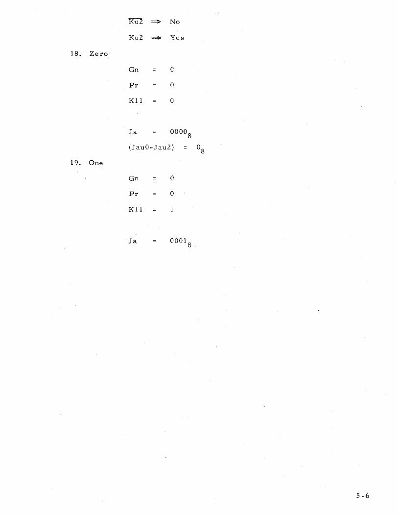
18. Zero
19. One
Ku2 ~ No
Ku2 ~ Yes
Gn = 0
Fr - 0
K11 = 0
Ja =
(JauO ... Jau2)
Gn =
Pr =
Kll =
Ja =
o
o
1
=
5-6

CHAPTER 6
Basic Internal Operations
6. 1. Introdu ction to timing charts
6.2 End
6. 3 Operand assembly
604 Trap
6. 5 Basic opcode S

6. 1 Introduction to timing charts
The opcodes will be described by means of timing charts. A timing
chart is divided into machine cycleso Each machine cycle is headed
by an identifying logical expression opposite which are li~ted the
events that occur throughout that cycle. The three individual clock
times (Tl, TO, Tp) then follow-opposed by those events peculiar to
the given clock time. Both hardware implicit in the performance of
an event and the timing of some of the signals are listed in parenthe se s
following the event. Explanatory notes are bracketed and appear,
indented, immediately underneath the event they expound.
In order to obtain a complete picture of an opcode it will be ne ce s sar y
to mentally superimpose the End tiITling chart and the appropriate
operand asseITlbly timing chart upon the timing chart of the given opcode.
6.2 End
During the last phase of every opcode, preparations must be made for
the next instruction. These preparations are effected by the signaJ
End ..
Most opcodes hold End true throughout the last phase of their execution.
However, those opcodes which change the instruction sequence (viz.
BRANCH instructions, EXECUTE instructions, and TRAPPING instructions)
obviously will not gate
P-S.
This is avoided by having these exceptional opcodes bring up End only
at Tp time of their last phase (which, in fact, is always qD).
End
End lnt
Tl P-S
[Access the next instruction from the address in p] 6 -1

TO
Tp ffi ==> A~B
[Restore A and B - During operand assembly (qD),
Or caused A. and B to be swapped]
M-C (Jm)
[i. e. next i.nstruction-C]
(MO-M.5}-O (Jm)
[i. e. next opcode-O J
M6-Lp (Jrn)
[Set up Lp for qi)]
Set Fp
[Set Fpfor cji}]
Clear 010
[Clear the memory parity error indicator - in case a
transfer to IDLE is gated (see below). ]
Clear 011
[Set up for a possible transfer to IDLE (see below)]
(Ht + Ip)~· Set Cpe
[Check parity of the next instruction]
Go to <ji)
[Perform the next instruction]
Ht Ip ~Go to cf>l (more precisely, </>1 on Ht)
[~DLE - Note that the HALT flip-flop, Ht, m.ust
be set and this (1P) mu st not be the End phase of
an EXU opcode or a trapping opcode. ]
6.3 Operand assembly.
The initial decodin~ of eve:r:y instruction is similiar. This similarity
exte:tlQs from the read-out of the instruction to the referencing of memo:ry
6 .. 2

at the effective address~The term OPERAND ASSEMBLY vvill be uSed
to refer generally to the whole breadth of this initial decoding.
Operand assembly takes place in q:o conversely, q:o is only entered for
operand· assembly.
Some of the genera.l purpose flip-flops used in <j:D include:
Fp Fp signals that the current cycle through q:o is
processing the first word of a (possible) instruc
tion word pair. Fp signals that the current cycle
through q:o is processing the second word of an
instruction word pair.
Lp
Ip
09-011
010
Lp signals that the current cycle through q:o
wJl1 conclude operand assembly.
Ip is examined at <Ii> T 1 0 During q:o Fp, it will
block any change of P; durjng <j:D Fp, it will gate
indexing (as opposed to no indexing).
09,010, and 011 will temporarily (during q:o Fp
Tl) hold the most significant 3 bits of any 15 bit
address.
o lOis also uE;ed (at q:o Fp Tp) to effe ct (via S + 1 ~
P) updating (effectively P + 2~P) of P for double
word instructions 0
011 011 is also used (at q:o Lp Tp) to gate the conclusion
(viz; S~P, End) of the opcodes which change the
instruction sequence.
The adder (Ja) is used at TI and Tp times by the operand assembly
logic. The adder is reserved at q:o TO time for use by the particular
opcodes. These q:o TO uses of the,adder, as well as all other qD events
6-3
peculiar to certain opcodes, are described under the particular opcode.
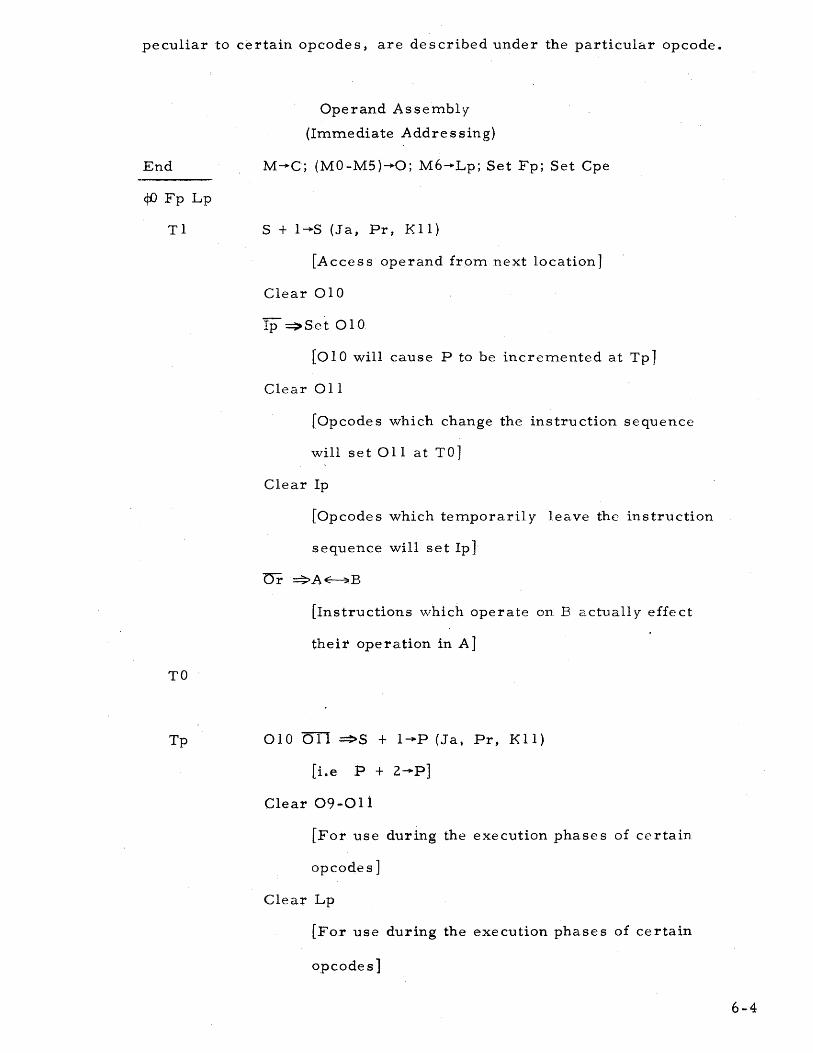
End
qD Fp Lp
Tl
TO
Tp
Operand Assembly
(Immedia.te Addressing)
M-C; (MO-M5)-0; M6-Lp; Set Fp; Set Cpe
S + 1 -S ( J a , Pr, K 1 1 )
[Access operand from next location]
Clear 010
Ip :::;:. Set 010
[010 will cause P to be incremented at Tp]
Clear all
[Opcodes which change the instruction sequence
will set a 1 1 at TO]
Clear Ip
[Opcodes which temporarily leave the instruction
sequence will set Ip]
[Instructions \vhich operate on B actually effect
their operation in A]
010 CIT! =!>S + I-P (Ja, Pr, K11)
[i.e P + 2-P]
Clear 09-011
[For use during the execution pha.ses of certain
opcodes]
Clear Lp
[For use during the execution phases of certain
opcodes]
6-4

End
<f{) Fp Lp
TI
TO
Tp
Leave Fp set
[For use during the execution phase s of certain
opcodes]
Operation Assem.bly
(Direct Scratch Pad Addressing)
M~Ci (MO-M5)-O; M6--Lp; Set Fp; Set Cpe
Ip~ S + I-P" ,(Ja, Pr, KII)
[i. e. P + I-P]
( C , • . . , 0, C 7 , Or • • , ell )-S
[A,ccess operand from. scratch pad1
Clear O}O
[010 would gate the incrementing of P at Tp]
Clear 011
[Opcodes which change the instruction sequence
will set 011 at TO]
Clear Ip
[Opcodes which temporarily leave the instruction
sequence will set Ip]
Or =!If A f---+ B
[Instructions which operate on B actually effect
their operation in A}
Clear 09-011
[For use during the execution phases of certain
opcodes]
6-5

End
cjD Fp Lp
Tl
TO
Tp
Clear Lp
[For use during the execution phases of certain
opcodes]
Leave Fp set
[For use during the execution phase s of certain
opcodes]
Operand Assembly
(Full Direct Addressing)
M-C; (MO-M5)-0; M6-Lp; Set Fp; Set Cpe
S + 1 -S (J a ~ Pr, K 11 )
[Access bottom 12 bits of the effective address]
Clear 010
Ip =>Set 010
[010 will gate the incrementing of P at Tp]
Clear 011
[011 would gate a change in the instruction sequence
at TpJ
Clear Ip
[Ip gates the proper setup of S at cjD Fp Lp T 1]
010 ~ S + 1-P (J a, Pr J K 11 )
[i. e. P + 2-P]
(C9-C 11 }-(09-0 11)
[Save the upper 3 bits of the effective address]
6-6

<ji) Fp Lp
Tl
TO'
M-C (Jm)
[The bottom 12 bits of the effective address go
to C]
Set Lp
[The next cycle through cjD will be the last]
Clear Fp
[The next cycle through cjD will be to process
the second word of an instruction word pair]
Set Cpe
[Check parity of these bottom 12 effective
addre ss bits]
Ip ~ (09, 01 0, 01 1, CO, ..• , C 1 1 )-S
[Access the operand]
Clear 010
[010 would gate tl-;e incrementing of Pat 1'p]
Clear 011
[Opcodes which change the instruction seq\]ence
will set 011 at TO]
Clear Ip
[Opcodes which temporarily leave the instruction
sequence will set Ip 1
Or :=.:;:.A~B
[Instructions which operate on B actually effect
their operation in A]
6-7
Tp
End
<ji) Fp Lp
Tl
TO
Tp
Clear 09-011
[For use during the execution phases of certain
opcode s]
Clear Lp
[For use during the execution phases of certain
opcodes]
Set Fp
[For use during the execution phases of certain
opcode s]
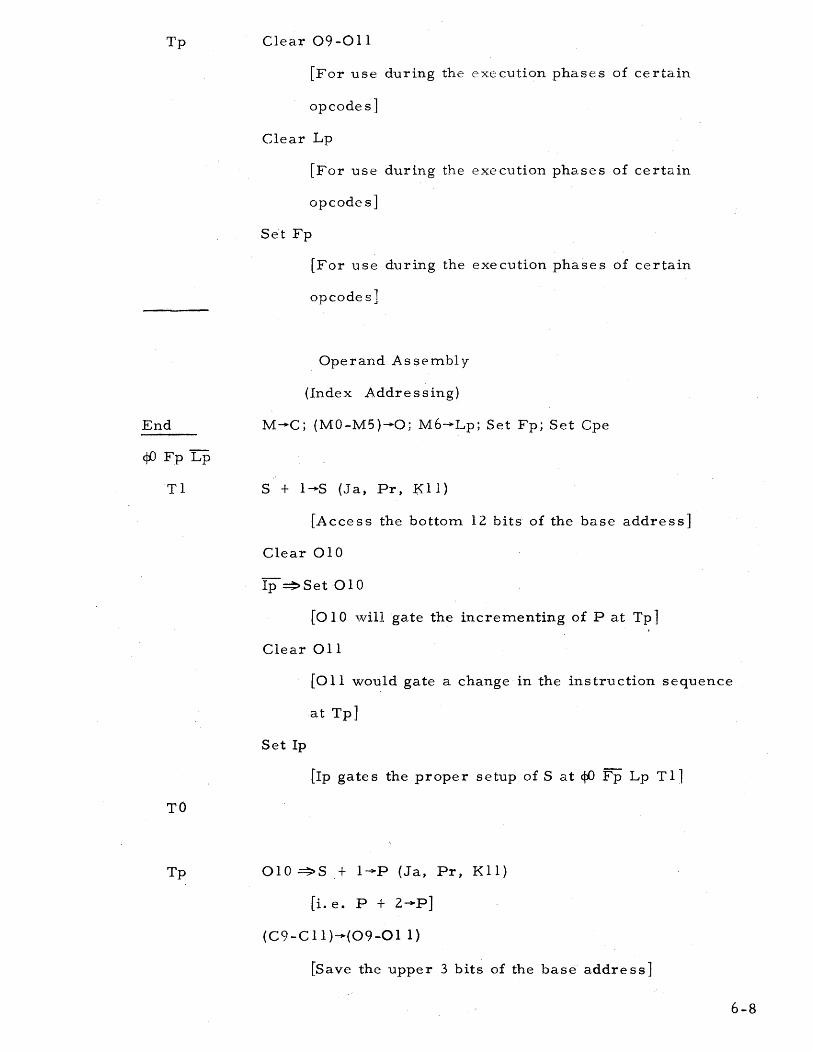
Operand Assembl y
(Index Addressing)
M-C; (MO-M5)-0; M6-Lp; Set Fp; Set Cpe
S + l-S (J a, Pr, K 1 1 )
[Access the bottom 12 bits of the base address]
Clear 010
Ip ~Set 010
[010 'will gate the incrementing of P at Tp]
Clear 011
[011 would gate a change in the instruction sequence
at Tp]
Set Ip
[Ip gate s the proper setup of S at <ji) Fp Lp T 1]
o 1 0 ~ S + 1-P (J a, Pr, K 11 )
(i. e. P + 2-P]
(C9-Cl1)~(09-011)
[Save the upper 3 bits of the base addre ss]
6-8

1'1
TO
Tp
M-C (Jm)
[The bottom 12 bits of the ba.se address go to cl
Set Lp
[The next cycle through cj:D wi";l be the last]
Clear Fp
[The next cycle through cji) will be to proce s s the
second word of an instruction word pair]
Set Cpe
[Check parity of thesebottcm. 12 base address bits]
/"
Ip ::::=}1(09, 010, 011,COJ •. o~C11)-{O,0,0,AO, .. o,All)~-S \.
[A'ccess the operand]
Clear 010
[010 would gate the incrementing of P at Tp 1
Clear 011
[Opcodes which change the instruction sequence
will set 011 at TO]
Clear Ip
[Opcode s which tempor aril y Ie ave the ins tru ction
sequence will set Ip]
[Instructions which operate on B actually effect
their operation in A]
Clear 09 -0 11
[For use during the execution phases of certain cpcodcs]
6-9

End
<Ii> Fp Lp
Tl
TO
Tp
Clear Lp
[For use during the execution phases of certain
opcodes]
Set Fp
[For use during the execution phases of certain·
opcodes]
Operand Assembly
(Full Indirect Addressing)
M-C; (MO-M5)-0; M6-Lp; Set Fp; Set Cpe
5 + 1 -S ( J a , P r, K 1 1 )
[Access bottom 12 bits of the indirect address]
Clear 010
Ip ~=>5et 010
[010 will gate the incrementing of P at Tp 1 .
Clear all
[011 would ga.te a change in the instruction sequence
at Tp]
Clear Ip
[Ip gate s the prope r setup of S at <ji) Fp Lp T 11
010:=::;>5 + 1-P (Ja, Pr, Kll)
[i. e. P + 2-P]
(C9-Cl1)-(09-0Il)
[Save the upper 3 bits of the indirect address1
M-C (Jm)
6-10

Tl
TO'
Tp
[The bcttonl L:: bits of the indirect address go to C]
Leave Lp clear
[ fhe n~xt cycl~ through ¢e wD.L not be the last]
Clear Fp
[The next cycle through ¢O will be to process the
second word of an instruction wcrd pair']
Set Cpe
[Check parity of t:',ese bottom 12 indirect address bits]
::p~(09t 010, all. CO, ... , Cll)-S
[ACCess the indirect instriJction]
Clea.r 010
[010 would ga.te the incrementing of P at Tp]
Clear all
[all would g&te a change in the instruction sequence
at Tp]
Set Ip
[Ip vvill block an y changE' to P durin g the nQxt <jD J
M-C (Jm)
[Indire ct ins tr ,I c tion goe s to C]
M6-Lp (Jm)
[R e -initialize L:;.l
Set Fp
[R . 't' .,' . e-lnl laL17~I," FJ p,
6-11

End
qi) FpLp
Tl
TO
Tp
Set Cpe
[Check parity of the indirec~ instruction]
Stayin qi)
[Operand assembl y begins again]
Operand Assembly
(Indirect Scratch Pad Addressing)
M-+C; (MO-MS)-+O; M.6-+Lp; Set Fp; Set Cpe
Ip.~S +.l-+P (Ja, Pr, Kll)
[i. e. P + l-+P]
(O, •.• ,O, 1, C9~ ClO, CII, O)-+S
[A·ccess the indirect instruction]
Clear OJO
[010 would gate the incrementing of P at Tp]
Clear 011
[011 would gate a change in the instru.ction sequence
at Tp]
Set Ip
[Ip will block any changes to P during the next qi)]
M-+C (Jm)
[Indirect instruction goes to C]
M6-+Lp (Jm)
[R e -initialize Lp]
Leave Fp set
[R e'-initialize FP]
£:> .. 12

6.4 Trap
Set Cpe
[Check parity of the indirect instruction 1
Sta y in cjl)
[Operand assetnbly begins aga.in]
Logical provisions have been made to TRAP certain opcodes instead
of exe cuting them norlTIall y. When trapping a given opcode, all norlTIal
operations are inhibited; the P register is not increlTIented. Instead, the
instruction (pair) at a uniquely defined location pair is executed. The
instruction at the trap address will normally be a BMC/BRM to a trap
subroutine; since the P register contains the address of the first word
of the trapping instruction (pair), proper linkage between the trap sub
routine and the· trapping instru ction is established.
DVX (12/52) and MUX (13/53) are optional instructions. If the option
is installed, these instructions will never trap~ If the option is not
installed, these instructions will always trap.
POT/BOT (10/50), WOT/ROT (II/51), PIN/BPI (14/54), and WIN/RIN
(15/55) lTIay operate normally (Pet) or trap {Pet}. The progralTI controls
the operation via Pet.
The trap address pairs have been defined as follows:
Opcode Address
POT (10)' 00130
BPO (50) 00132
WOT (11) 00134
ROT (51) 00136
6-13

End
cji) Tr
Tl
TO
Opcode Address
DVB ( 12) 00120
DVA (52) 00122
MUA (13) 00124
MUB (53) 00126
PIN (14) 00140
BPI (54) 00142
WIN (15) 00144
RIN (55) 00146
M-C; (MO-M5}-0; M6-Lp; Set Fp;Set Cpe
Tr = FetOl 02 04 + Option CIT 02 03 04
Block all normal transfers to Sand P.
[Thus P remains pointing to the trapping instruction]
TRAP ADDRESS-S
Set Ip
[Access the instruction at the trap location]
[Ip will block any change of P during the next qi). Thus
the instruction at the trap address is truly executed
(a la·mode de EXU)]
Block the possible interchange of A and B
[cji) Lp Or would have gated this interchange 1
Block thepossib1e clearing of A
[(¢D Lp) (01 02 03 04 05) would have gated this
clearing. But (01 0203 04 05) is held at ground
when the M·UX/DVX option is absent.]
6-14

Tp End (only at IIp)
(End gates the preparation for the next instruction]
Block the possible increment of P
[cji) 010 would have gated this increm.~nt]
Block the possible interchange of A and B
[End Or would have gated this interchange J
Block a1l set pulses to Lp that are not gated by Jmb
[End will, as alwa ys, transfer Jm6 to Lp]
6. 5 Basic opcode s
. CYX, CYD, CFX, CFX.) CFD
(02/42, 03/43)
The shift commands (02/42, 03/43) have the capability to effect both
single-register and double-register shifts. All shift commands have
the following common general structure:
1. All shifts are left circular.
2. 0::;' shift count 5.. 17 8
3. The least significant four bits of the effective address (E 11-
E 14) determine the shift count-these four bits should contain
the lIs complement of the desired shift count.
4 •. The fifth least significant bit of the effective address tElO)
determines whether the shift ·will be single -register or
double -register:
E10 ~single-register shift
E 10 :-_--===>double-register shift
5. Thus, the operation of a particular shift oI)code is completely
determined by the least significant five bits on the effective
address (E10-EI4).
6-15

cpo Lp
T1
TO (SO-SlI)-C (Ja, Pr)
Tp
[i. e. Cornplemented shift count-{e8 -C 11)
Shift indicator-C7]
(C B,.. C 11 t 11112
) =:::} C + I-C (J a, Pr, K 11 )
[Increment shift count if terminus
has not yet been reached]
Shift A left one binar y po s ition
[A is shifted during all SHIFT opcodes]
(CB -C 11 I- 11112
) C7::=:;> Also shift B left one binar y position
[B is shifted only during double-register SHIFT opcodcs]
( C B - CII f. 11 112
) C YX ::::::> A 0-A 11
[X is shifted left cir cu1ar ]
(CB-CII 1111 ) CFX =*AO-F( 2
[F,;' ,X) is shifted left circular]
(CB-Cl1 t- 11112
) CYD ==>BO-A11
AO-+B 11
[(A, B) is shifted left circ111ar]
(CB-C11 t 11112
) CFI ~BO-All
6-16
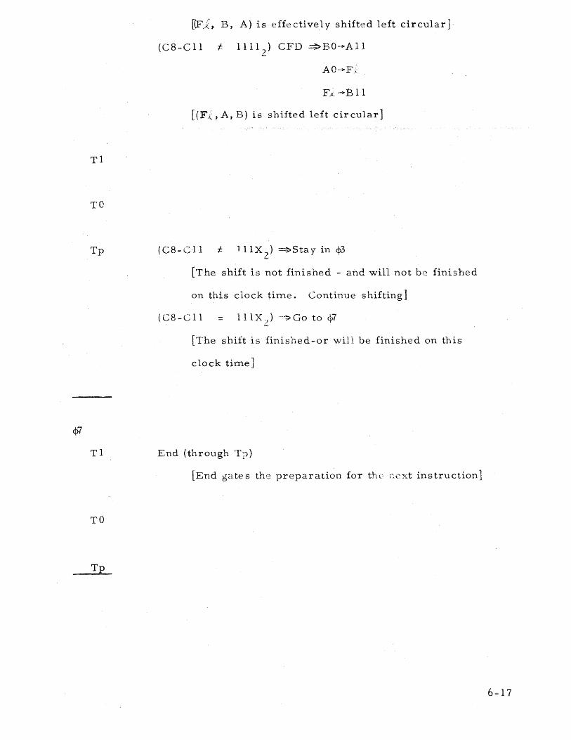
T1
TO
Tp
<1>7
T1
TO
Tp
[(F,i J B, A) is effe cti ve 1 y shifted left cir cu1ar:l
(CB-Cll f:. 11112
) CFD ~BO-All
AO-FJ
F;.-Bll
[(F . .c, A, B) is shifted left circular J
(C8-Cl1 f:. 111XZ
) :::::::>Stay in cp3
[The shift is not finished - and will not be finished
on this clock time.. Continue shifting]
(C8-C11 = lllX2)-:~>Go to cp7
[The shift is finished-or will. be finished on this
clock time]
End (through TT»
[End gates the preparation for tht.' r:ext instr·llction]
6-17

cji) Lp
Tl
TO
_ Tp
¥>
Tl
TO
Tp
c!D Lp
Tl
TO
Tp
STX
(04/44)
Mw (through Tp)
[ The memor y reference of the effe cti ve a.ddre s s
thus becomes a write cycle]
A-M (Jm-through Tp)
[A will be written into memory]
End (thr'ough Tp)
[End ,gates the preparation for the next instruction]
COX, CEX, CMX
(05/45, 06/46, 07/47)
M-C (Jm)
[i. e. ope'rand-C]
6-18

Tl
TO"
Tp
Set Cpe
[Check parity of the operand]
COX:~AC-Gn
AC-Pr
[Thus any AC will result in Ku2]
CEX =?>A (t; C-Gn '-....
A(j) C-Pr
[Thus a difference of bits in any corresponding
position of A and C will result in Ku2]
CMX ~ffect a norrnalsubtract (Gn, Pr, Kll)
[Thus A 2.c will result in KuZ]
[Whence F;" :::::>(X) 1\ (E) t- 1 anYV/here]
CEX ~Ku2-F,"
[Whence F[ ::::;> (X) f. (E)]
CMX ~Ku2-F";~
[Whence FC~(x» (En
End (through Tp)
[End gate s the preparation for the next instruction]
6-19

DVX
(12/52)
The divide operation is entirely straightforward. :n essence the
internal logic performs the division
(A, B) ~ (C)
The logic will initiall y as sume that
(A) <: (C)
the division can then be effected by 12 (trial) subtract operations.
These subtractions will always take place in A. This means that
(A, B) must be shifted left one binary position before each subtraction.
This allows the quotient to be inserted, a bit at a time, intoB from the
least significant end (B 11). In fact, the left shift of A will preceed the
left shift of B. This will allow the quotient bit to be inserted into B at
the time of B I S left shift.
A divide step consists of:
1. Shift A. left one binar y po s ition
AO-09
:EO-All
2. Try subtracting C from (09, A). (The logic need only su~)tract
C from A.) The subtraction will be possible either if 09 = lor
Ku2 = I (Ku2 is the borro\v out of the subtr2.ct operation A-C).
3. Shift B left one binary position 41uotient bit ;;; 09 + Ku2-B 11).
If the subtract is possible (i. e. quotient bit = 09 + Ku2 = 1),
then replace A \vith the new partial remainder (viz. A -C).
If the above sequence is done a total of 12 times (this divide step count
will be made in S) J the re suI ts will be:
1. The final quotient, properly shifted, in B
2. The final remainder in A
6-20

The 12 dlviae steps are sumewhat ol..;.ie,j:entiatea OJ. r y and Lp:
qi) Lp
Tl
TO
·Tp
T1
Fp Lp Divide Step
1 0 1st
0 0 2nd through 11th
0 1 11 th
1 1 12th
M-+C (Jm)
[i. e. ope rand
Set Cpe
divisor-+C]
[Check parity ot theopera.nd]
Shift A left one binary position
[This is the start of a divide step 1
A 0-+09
[Save the most significant bit of A for the ensuing
subtraction]
BO-.Al1
[This consumrn.a te s the left shift of A]
Fp Lp ~ l-+S (J a, K 11 )
[Fp \1;/as left set and Lp Vias left reset by qi).
This initialize s the divide step count to 1 1
6-21

TO
Tp
Fp Lp :;~5 + 1-5 (Ja~ Pr, K11)
[This increments th~: divide step count]
Fp Lp .~ End (through Tp)
[This is th<:; 1(~. st di vide s tl'P - End gate s the
preparation for the next instruction]
Effect a norma] subtract operation (through Tp - Ja,
Gn, Pr, Kll)
[Ku2 win be examined at Tp to see if this subtraction
is possible]
(58-511 ;::: 1Xl12
) ~5et Lp
[This is the penultimate divide step - Fp Lp will
gate End throughout the last divide step 1
Shift B left one binar y position
[A had already been shifted at T 11
(09 + Ku2)-B 11
[i. eo quotient bit-P 11. This consummates the
left shift of B 1
(09 + Ku2) ~~','> Ja-A
[i. eo A-C-A. This places a nevv (partial) remainder
in A 1
Clear Fp
[Fp Lp had gated the initialization of the divide step
count]
Lp~5etFp
[This is the end of the penultima.te divide step and
conc]udes the preparations that will allow End to be
true throughout the last divide step 1
End ~E·lock the possible interchange of A and E
[This interch2ngc, normally g.:.ted by End C;;, \vould
have interfcrre:d with other A and B register transfers. 1 i ?., t) .... '- ,.:..,.

·MUX
(13/53)
The multiply operation is achieved, quite directly, by 12 additions. In
essence the internal logic performs the multiplication
(B) • (C)
by the following steps:
1. elecr the partial product {A)
2~ Examine the least significant bit of the multiplier (B 11)
3. If Ell = 1, addCtoAandplacethesuminA.
If p 11 = 0, do nothing.
4. Shift the partial product (A) right one bit position. If B 11 =1,
place the carry from the above addition (A + C) in AO~ If B 11
= O. place zero in AG.
'5. The bit shifted out of the least significant end of A is the least
significant bit of the final answer. It can not be changed by any
further additions.
6. Shift the multiplier (B) right one bit position. Place the final
answer bit (that V>Tas shifted out of A) in BO. The former con
tent ofB 11 (the least significant multiplier bit) are lost; it
has been used and is no longer needed.
7. Since both the multiplier and partial product have been shifted
. right one bit position, we are in a position to return to step 2
to process the second least significant bit of the original multiplier.
By perfo.rming steps 2-6 (above) a total of 12 times the multiplication is
accomplished. The final answer appears in (A, B).
Because of shifted transfer paths, the internal logic can perform a complete
addition and shift in one clock time. Therefore, after the multiplicand has
been accessed, only 4 machine cycles are needed to complete the
6-23

Fp and Lp:
<Ii> Lp
Tl
TO
Tp
Fp Lp Count
1 0 1
0 0 2
0 1 3
1 1 4
[This initializes the partial prod"llct to zero.
effected by directly pulsing the enable, Ag 1
M-C (Jm)
[i. e. ope rand = multiplicand -C]
Set Cpe
[Check parity of the operand]
BII:::::::;'>Effect a normal add operation (Ja, Gn, Pr)
[i. e. A + C-Ja]
Bil =>A-Ja (Pr)
[Note that, in this cas/e, Ku2 = 0]
Ja {shifted right one binary position}-A
Ku2-AO
[This gives us a new partial product 1
Shift B right one binary position
or • . tt. IS
[This repositions the next multiplier bit at B 11 and
makes room for a final product bit at BO] 6-24

Tl
TO
Tp
qi) Lp
Tl
TO
Tp
Jall-BO
[i. e. final product bit-BO]
Fp Lp ~ End (through Tp)
[End gates the preparation for the next instruction]
Lp ~ Clear Fp
[This changes the count from 1 to 2]
Fp :::;> Set Lp
[This change s the count from 2 to 3 J
Lp~SetFp
[This changes the count from 3 to 4]
End~ Block the possible interchange of A and B
[rhis interchange, normall y gated by End Or,
would have interferred with the Ja (right shift)-A
and B (right shift)-B transfers at this time]
M-C (Jm)
MPO/MPF
(16/56)
[i. e. operand-C)
Set Cpe
[Check parity of the operand]

Tl
TO
Tp
Tl
TO
Tp
ctD Lp
Tl
TO
Tp
MPO ~l-Kll
MPF ~FJ. -Kll
C + K 1 l-C (J a, Pr, K 11 )
[The operand h,~ s been P!operl y incremented 1
Ku2-:W,l
[i. e. carry out-Fi]
Mw (through Tp)
[This memory cycle will be a write cycle 1
C-M (Jrn - through Tp)
[The incremented operand will now be returned to
rnernor y]
End (through Tp)
[End gates the preparation for the next instruction]
M-C (Jm)
XMF, LDF
(17/57)
[i. e. operand-C]
6-26

TI
TO
Tp
</>7
TI
TO
Tp
<jD Lp
TI
Set Cpe
[Check parity of the operand]
C-c (J&, Pr)
[This is a hard,vare quirk}
Mw {through Tp}
[This memory cycle will be a. write cycle]
XMF =>(FC, C I-C 11 }-M (Jm-through Tp)
[F; will be 'i7 ... .'ritten into the most significant bit of
the operand (along \vith the other original eleven
bits)]
LDF ~C-M (Jm - through Tp)
[Thus LDF (needlessly) rewrites the original operand
back into memor y]
End (through Tp)
[End gates the preparation for the next instruction]
Co -F)_
[The most significant bit of the operand has been
loaded into ~L]
SUX, sex
(20/60, 21/61)
6-27

TO
Tp
Tl
TO
Tp
qi) Lp .
Tl
TO
Tp
M-C (Jm)
[io e. operand-C]
Set Cpe
[Check parity of th.e operandl
S UX ::::::;> 1 - K 1 1
SCX~IT-Kll
A-C-Kfl-A (Ja, Gn, Pr, KIl)
[The subtr a ction has be en prope r 1 y pe rfo rm,~ d]
Kuz-£l
[i. e. borrow out-~-C.]
End (throu gh Tp)
[End gates the preparation for the next instruction]
M-C (Jm)
ADX, ACX
(22/62, 23/63)
[io e. operand-C]
6- 28
T]
TO
Tp
eli) Lp
TI
TO
Tp
TI
Set Cpe-
[Check parity of the operand]
ADX =:;> O-K 11
ACX =;>£t-KII
[A hard\vare quirk caus-:::'s F{ -Kll to be a.lso gated
by 011; however, 011 was left cleared by cjD Lp 1
A + C + K 11-A (J a) Gn, Pr, K 11 )
[The addition has been properly performed]
Ku2-F..-L
[i. e. carry au t-F 1J
End (through Tp)
[End gates the preparation for the next -instruction 1
LDX, ANX, EOX, ORX
(24/64, 25/65, 26/66, 27/67)
M~C (Jm)
[i. e. operand-C1
Set Cpe
[Check parity of the operand]
LDX 9C-A (J2.., Pr)
[The LOAD has been performed]

TO
Tp
<ji) Lp
Tl
TO
Tp
ANX=;;>AI\C-A (Ja, Pr)
[The AND has been performed]
EOX ~A G) C-A (Ja, Pr)
[The EXCLUSIVE OR has been performed]
ORX ~AvC-A (Ja, Pr)
[The INCLUSIVE OR has been performed]
End (through Tp)
A~B
[End gates the preparation for the next instruction]
BAX
(30)
[This is gated, as always,. by qi> Lp Or]
Set 011
[011 will gate the completion of this opcode at Tp]
all ===>End (only at Tp)
[End gates the preparation for the next instruction
which is actually the operand currently being read
from. mem.or y 1
s--p (Ja. Pr)
[i. e. effective address-P; the branch is made]
End .::::=;>Block the interchange of A and B
[By blocking this interchange, norm.ally gated by
End Or, A and B rem.ain swapped (see Tl above)]
6-30

ql) Lp
Tl
TO
Tp
<\>7
TI
TO
Tp
BDA
(70)
A-I-A (Ja, Gn, Pr)
[This decrements A]
Ku2~Set 011
[If tbe decremc'nted contents of A are unequal to
7777e: then the' branch is taken (gated at Tp by Oll)J
Ku2. ~Leave 011 clear
[If the d~·'cremented contents of A are equal to 7777 8 ,
then the n(:"-xt instruction in sequence will be taken]
o 11 ~ End (only at Tp)
[End gates the preparation for the next instruction
which is actually the operand currently being read from
memory]
S-p (Ja, Pr)
[Leo effective address-Pi the branch is taken1
End =--=> Go to <1>7
[The branch was not taken - the r ... cxt instruction in
sequence must be accessed]
End (through Tp)
[End gates the preparation for the next instruction]
6-31
qi) Lp
Tl
TO
Tp
cp7
Tl
TO
Tp
BFF, BFT
(31/71).
BFF!\'F[ + BFT!\FL=}Set all
[If Ff. is in the condition being te sted for, the
branch is taken (gated at Tp by 011)]
BFFI\FJ. + BFT!\'F1. ~ Leave all clear
[If Flis not in the condition being tested for,
the next instruction in sequence will be taken]
all ~End (only at Tp)
. [End gates the preparation for the next instruction
which is actually the operand currently being read
frotn tnetnory]
S-P (Ja, Pr)
[i. eo effective address-P;the branch is taken]
End =';> Go to cp7
[The branch was not taken-the next instruction in
sequence tnust be accessed]
End (through Tp)
[End gates the preparation for the next instruction 1
6-32

<ji) Lp
Tl
TO
Tp
~ Fp
Tl
TO
Set Ip
EXU
(72)
[Ip wiLl block any change of P during tr .. 2 };0XL qD.
Thus the instr'uction at tr .. c effective address is
truly EXECUTED]
Set 011
[011 will gate the comple tion of this opcode "t Tp 1
o 11 ~End (only at Tp)
[End gates the preparation for the n(:xt instruction
which is actually the operand currently being rLad
from rr..ernor 1]
Block n:-e tra:rlsfer cf S ;;0 P
[Ip 'will actually block this transfer. This transfer
(normally gated by 011) must be blocked because
EXU only leaves the instruction sequence to execute
this one instru ction 1
BRL) ERU
(33/73)
BRL~CO-F_;..
[This loci.ds F,_ from bit 0 of the first \~/ord of an
instruction \:~~ith('r direct or indirect)]
6-33

Tp
¥> Lp
TI
TO
Tp
qfl Lp
Tl
TO
Tp
Cl-Pct
[This loads Pct from bit 1 of the first word of an
instruction (either direct or indirect)]
Note that this machine cycle could be concurrent with
qo Fp above.
Set 011
[011 will gate the completion of this opcade at Tp]
011~End
[End gates the preparation for the next instruction
which is actually the operand currently being read
from. mem.or y]
S-P (Ja, Pr)
[1. e. effective address-P; the branch is taken]
M-C (Jm)
XMX
(34/74)
[i. e. operand-C]
6-34

Set Cpe
[Check parity of the operan~]
Tl C-c (Ja, !?/r)
[This is a hardware quirk]
TO . Mw (through Tp)
. Tp
<\>7
Tl
TO
Tp
~ Lp
Tl
TO
Tp
[This memory cycle \vi11 be a write cycle 1
A-M (Jm - through Tp)
[The register is stored at the effective address]
C-A (Ja, Pr)
[The operand j.s stored in the register]
E:nd (through Tp)
[End gates the preparation for the next instruction]
M-C (Jm)
MAX
(35/75)
[i. e. operand-C]
6-35

Tl
TO
Tp
cf>7
Tl
TO
Tp
~ Lp .
Tl
TO
Tp
Set Cpe
[Check parity of the operand]
AAC-+C (Ja, Pr)
[The AND has been performed}
Mw (through Tp)
[This memory cycle will be a write cycle]
C-+M (Jm- through Tp)
[The AND result is returned to memory]
End (through Tp)
[End gates the preparation for the next instruction]
M-+C (Jrn)
MPX
(36/76)
[1. e. operand-+C]
6-36

Tl
TO
Tp
Tl
TO
Tp
qD Lp
Tl
TO
Set Cpe
[Check parity of the operand.]
A + C-C (Ja, Gn, Pr)
[The addition has been performed]
Ku2-E£
[i. e. carr}' out-£L]
Mw (through Tp)
[This memor y cycle \vill be a write cycle]
C-M (Jm - through Tp)
[The sun~ is returned to memory]
End (through Ip)
[End gates the pr('paration for the next instruction]
BMC, BTIlvl
(37/7 i')
Mw (through Tp)
[The memory refer:'IV'? of Il~J(' ,>'!J,'ctive addrcos
thus becomes (j writ,- cycle!
6-37

Tp
TI
TO
Tp
4>7
1'1
TO
Tp
(Ft, Pet, 0, .•• ,0, PuO, Pul, Pu2)-~A (Jm - through Tp)
[The first word of the mark is stored at the effective
address}
s + l ..... S (J a, Pr, K 1 1 )
[The ensuing memory reference will b~ at the
effective address + 1]
Mw (through· Tp)
[The ensuing memory cycle will be a write cycle 1 (PO-PI 1 )-M (Jm - through Tp)
[The second word of the mark is stored at the
effective addre s s + 1]
s + 1 ..... P (J a, Pr, K 11 )
[i. e. effective address +Z ..... p; the branch is ma.de]
BMC ~ Clear ~.l
Set Pet
End (through Tp)
[End will gate the preparation for the next instruction
which will be located in the effective address + Z (P
was set to this address at q,4 Tp)]
6-38

CHAPTER 7
Console Operations
7. 1 Introdu ction
7. Z Register display/alteration
7 ~ 3 Console functions
7. 4 Fill
7. 5 Miscellaneous switches
7. 6 Lights

.N'[It.Uftr
.... Lf OW"fllED
--FIll-- ••
Model ( ~o~puter Control Panel

7. 1 Introdu ction
A unique phase is entered and remained in when not performing opcodes.
cj>l is this IDLE phase. The computer may enter IDLE because of any of
the following.:
1. The operator depresses the RESET button. [St will gate an
immediate IDLE. ]
2. The operator moves the RUN -IDLE-STEP switch from R UN to
IDLE. [Ht will gate an IDLE at the completion of the current
instruction (End Tp).]
3. The operator STEP's an instruction. [Htwill gate a return to
IDLE at the completion of the instruction. (End Tp). ]
4. A HALT instruction is executed by the program. [i-It will gate
an IDLE at the completion of the HALT instruction (End Tp). ]
5. A memory. pa,rity error halt occurs. [ep Kp will gate an imme
diate IDLE. ]
cpl has been divided into four subphases:
cpl 011 Bt
cj>l 011 Ht
cj>l 011 Ht cpl 011 Ht
End Ht Ip
cj>l 011 Ht
This is the subphase of IDLE that is always entered
first. This is basically an interlocking subphase;
there is no way to leave the subphase unless certain
internal and external conditions are met.
This is the subphase of IDLE which allows the registers
to be displayed and their contents changed. This is also
the subphase which recognizes and instigates any console
function ..
These two subphases of IDLE execute every console
function.
M-C; Clear 010; Clear all
Clear 0
7-2

Tl
TO
Tp
[This clears 'out the opcode and initializes Or for
register display (see <1>1 all lit - Or ~ A and B
are home)]
Fp => Set Fp
[This initializes Fp for regfster display (see <pI all Ht
Fp would cause A and B to swap)]
Clear 09
[This forces C to be displayed on the REGISTER
DISPLAY lights during this subphase]
Clear Ip
[T.his initializes Ip for a return to instruction execution]
Clear Lp
[This initializes Lp for a possible FILL operation]
09 ~C-+REGISTER DIS PLA Y lights (Ja, Pr)
[The REGISTER DJSPLA Y lights are driven frolTI Ja]
010 ::::'>MEMOR Y PARITY light
010 ~HALT light
[A memory parity error halt will set 010]
(St + Tern) ~Mgm
[If either the com.puter is being reset (St) or the
memory stack is not up to a minimum operating
temperature (,fern), then a memory reference
will not be made]
-orO Kg KaKmi Kiilo Kpu st~ Set all
[If there is no memory parity error indicatiOtl (0 1 0),
all console functim switches are unactivated, and the
computer is not being reset (st); then go to subphase
<pI 011 Ht. ]
7-3

7.2 Register display/alteration
<!>1 011 Ht is the IDLE subphase which allows the contents of A, B, C,
and -P to be examined and changed.
A, B, and Care all displayed via the REGISTER DISPLAY lights. These
lights are actually driven from Ja. A or C may be directly displayed.
Since thel;"e is no way to put B on .Ta, B is displayed by interchanging A
and B and then actually displaying E from the A register. This operation
requires two flip ... f1ops:
Or
Fp
The Or flip -flop indicate s if A and Bare swappe d (Or)
or horne (Or).
The Fp flip-flop will syncronize the REGISTER DISPLAY
SELECT switch (A or B) with the internal display logic.
[Fp signals a change of the REGISTER DISPLA Y SELECT
switch. ]
A third flip-flop is used to control the actual register (A or C) currently
being displayed via Ja:
09 09 ~ display C
09 -~~ displa y A
The ad:ditional logic needed to alter the currently displayed register (A,
B, or C) are minor. The set buttons will also be placed on Pr; thus ORing
the m, at Ja, with the register currently being displayed. Finally,
Ja will be read back into the particular register. To clear the given
register, it is only necessary to block the gating that places the register
on Ja; then, when Ja is recirculated back into the register, all zeros will
be read in.
7-4

The P register display hdteration operates on the same principles asabave.
However, Ja is not used. TrePROGRAM LOCATION lights are driven
directly from P. P is directly recirculated. The set buttons are gated
dire ctl y into P.
Some of the pertinent console signals are:
Kb
Kb
Kc
Krp
The REGISTER DISPLA Y SELECT switch is requesting B
The REGISTER DISPLA Y SELECT switch is requesting A
or C
The REGISTER DISPLA Y SELECT switch is requesting C
The REGISTER DISPLA Y SELECT switch is requesting A
or B
The clear and set buttons should affect the PROGRAM
LOCA TION {F}
The clear and set buttons should affect the REGISTER
DISPLAY (A, B, orC)
Krc The clear button
KruO-Kru2 The fifteen set buttons
KrO-Krll
cj>1 Oll,Ht Clear 09
Kc=;:'Set 09
[09 will gate the display of A; 09 will gate the display
of C]
Clear Ip
[This initialize s Ip for a return to instruction exe cution]
Clear Lp
[This initializes Lp for a possible FILL operation]
7-5

C)9 :::-:::;;.iC (Krc + F:rp) + (SET BUTTONS) Krp Tpc' -.1 a.--+C (J~ Pr)
09 -::::::';;"'A (KTC + 1<: rp) + (SET BUTTONS) Krp Tp' -Ja-A (J a, Pr)
.Ta-:.- H·EGISTER lYfSPLA Y lights
[,Cr9 gates the display of C; 09 gates the display of A]
.. fp (J<rc + Kri:;)+· (SE'f BUTTONS) Krp)-P
P·-.PH OGHAIvILOCATION lights
rp :is displa.y-cd directly]
Tl P-:--s
[The ens'uing rnemory reference will thus be at the
addre S8' currentl y in p]
(Kb Or» ,.::::lezlr Fp
[1";) will gate a swap of A and B at TO]
TO
rTf the rnernory stack is not up to a minimum operating
terrlperature ('rem), then a memory reference will not
be rY\;:Lde 1
[Swa.p .A and B. The possible Ja-A tr .. :..Llsf.r at this
tircte rnust l)e blocked. ]
Toggle Or
[Or indi<:ateEl'whether A. and B are swapped (Or) or
bocne «Yiy]
Set Fp
[ThL~ A ar:,d I~ }tegister:~ now correspond to the REGISTER
Tp Terrl (f{ g .+. K.rni l<"rno + KPl.lt KS)7::'~ Clear Ht
[Th~':; rner:(j(y:'Y tack is at an operating temperature (Ten1)
and a CCn~H)j~) i\rnction has been requested. Go to 4>1 OllHt:
7··6

7. 3 Console functions
There are, basically, five console functions. Eacrl function generates
two signals frolTl its console switch. FrolTl the names given the two
signals, each signal of a pair appears to be the logical inverse of the
other. However, this is not the case. Whenever either signal of the
pair bounces true, its cOlTlplernent must already be stably false. These
signal pairs obviate any logical elimination of switch bounce.
l-<g, Kg Kg ~The H,UN/:DLE/STEP switch is at RUN.
This wili cause a return to the instruction sequence
be,ginning v"ith the instruction in the location specified
Kmi, Krni
Kmo, Kmo
Kpu, Kpu
Ks, Ks
by P.
Krni ~the MEMOR Y switch is at IN.
This \,vill cause the cont:~nts of C to be stored in the
location spe cified by P.
Kmo ~ The MEMOR Y switch is at OUT.
This will cause the contents of the location specified
by P to be read into C {and ,parity checked}.
Kpu ~The PROGHAM LOCATION switch is at
~:NCREMENT
This will cause P to be incremented by one. Then
the contents of the location specified by this newP
will be read into C (and parity checked).
Ks ~The HUN/IDLE/STEP switcr .. is at STEP
This will cause the execution of one instruction
the one in the location spe cified by P- follo\ved by
a return to IDLE.
7-7

cj>l all ill
Tl
, TO
Tp
RUN
(Kg)
S-S (Ja, Pr)
S-P (Ja, Pr)
[These are hardware quirks; P-S occured at every
T 1 time ofq,l 011 Ht]
Or ~ Clear Fp
[Or ~A· and B were swapped; 'FP will gate them
home at TO]
Fp ~A~B
[Swap A and B J
.Toggle Or
[io e. Clear Or - thus a is now completely clear]
Set Fp
[A and B are now home]
M-C (Jm,)
[This is a hardware quirk- the next instruction is
read into C and parity checked a whole machine
cycle before it is needed. In fact, End will gate a
repeat of the se operations during the next machine
cycle, cj>lorl Ht]
Set Cpe
[Check parity of the next instruction]
Clear 011
[i. e •. Go to cp1 trr1 ffi]
7-8

<jJ1 OITHt
Tl
TO
Tp
cp1 011 Ht
TI
TO
End (through Tp)
[End gates the preparation for the next instruction-
note that 0 is cleared, thus an interrupt cpuld be
recognized at this time]
End==.;;.Block the interchange of A and B
[End Or would have gated this interchange]
End Ht :;;:.Go to cji)
[Enter the instruction sequence and begin program
execution]
MEMORY IN
S~S (Ja, Pr)
S~P (Ja, Pr)
[These are hardware quirks; P-S occured at every
T 1 time of <jJ1 011 Ht]
Or => Clear Fp
[Or ~ A and B were swapped; Fp will gate them
home at TO]
Fp ~A~B
[Swap A and B]
Toggle Or
[i. e.· Clear Or- thus 0 is now completely cleared]
7-9

Set·Fp
[A and B are now home]
Mw (through Tp)
JThis memory· cycle will be a write cycle] ~ . • I
C .... M (Jm-througnTl')
[C will be written in:to ~emoryl
Tp C"C (Jm)
TI
TO
[This is a hardware' qil.irk]
Clear 011 ,
[1. e. Go to cp1 'OTIm]
Tp, .:Eii.Cr::; Set Ht
cp1 011 m Tl
I ..
[1. e. Retu,rn to cp1 on HtJ
MEMORY OUT,
, : (Kmo)
s---p'
[These are hardware quirks;, p...s occured at every
T 1 time 01 ... 011 Ht] .
Or ~Clear Fp
[OJ'''A and B were swapped; rp wilI'gate the'm
. ··home at TO]
7-10

TO
Tp
<1>1'<>';11 m 'Yl!
TO
Tp
~li O:l~l m. Tot
FP ==>A·~~B
[Swap Pi. and B J
Toggle Or
fi. e. Clear O:r -thus 0 is now completely eJea,redJ'
Set Fp
[A anq B are now home J
M~C (Jm)
[L e. operand-C; this performs, tbe des.irect memory
Toea~.".ou:tJ
s.et Cpe
[Check pa~ity of the operand}
Glee· aI" 0·11
Ei. e •. G,ot'o # oTt Htl
End =-~·S'et Ht
[i,. e. Return t,o $1 011 Btl
PROGR·A.M' RE'CiISTER !.NCR'EMEN:,]
(.Kpl).
s., + 1-8, (Ja", P'r,<. K 1:,1:)
5, +! li-llf:; (~.J:~", F?'~,. KJ'J:}· ..
[~'Qt}l:! ~i a-nd,: $~ are· ih'cr;emented'; byn Qr't:e' •. ,. Mrb;,t$\' tit:a1t
when entering this machine c:y;cle. Sr =, ~l' wa;SE·
aS$:ure,d~ since P'"-~S 0 ccu ~ed at; ev;er,y~ T.:t tim:e;· Q.:fI cpl.; G>Il;L Htr:
7':..11,

TO
Tp
~1 orr Ht
T1
TO
Tp
cpl 011 Ht
T1
Or~C1ear Fp
[Or ····c}> A and B were swapped; Fp will gate thern
home at 1'01
[Swap A. and .C::1
Toggle Or
[i. e. -=: 1 ear 0 r - tlAl.I~, 0 is no Vy' com l") 1 e tel y c 1 ear e d]
Set Fp
[A and Bare novv home 1
[i. e. operand->C; this performs the desired rnemory
read-out}
Set Cpe
[Check parity of the operand]
~~lear 011
[ , G t dlO-11 ffirl. 1. e • 0 0 ,) ~. J_ r' t j
End~Set Ht
[i. e. R e tu rn to <1>1 0 1 1 H t ]
STEP
(Ks)
S-S (Ja, Pr)
7-12
TO
Tp
cpl all Ht
Tl
S-+P (Ja, Pr)
[These are hardwa.re quirks; P-S occurred at every T 1
time of cj>1 all Ht]
Or '~Clear Fp
[Or :.:::!>A and B were swa.pped; 'FP will gate them horriE
at TO]
Fp --:'>A~-+ B
[Swap A and B]
Toggle Or
[i. e. Clear Or -thus a is now completel y cleared]
Set Fp
[A and B are nov! home]
M-C (Jm)
[This is a hardv,\fare quirk-the next instruction is
read into C and parity, che cked a vlhole machine
cycle before it is needed. In fact, End will gate
a repeat of these opE:rations during the next machine
cycle J cj>l on Ht]
Set Cpe
[Check parity of the next instruction]
Clear all
[i. e. Go to cj>l on Ht]
End (through Tp)
[End gates the preparation for the next instruction]
Block the' recognizing of any interrupts
[No interrupts are recognized while STEPPING]
7-13

TO
Tp
7. 4 Fill
End ~ Bio ck the inte r change of A an d B
[End Or would have gated this int(~rcha.t:gl·l
End m~Goto ¥l .
[Enter the instruction sequence a.nd ex,' c utf- OT..';'
instruction. ¥Kg will set Ht so that :T)LE io
re -entered at the End of this instruction 1
It is possible to automatically read in a nine word program. Thi~'
bootstrap process is called FILL. The nine word prograrr, 'will
usually be a stnall loader to bring in and execute a tnuch bigger
program. A FILL is effected as follows:
·1. Motnentarily ~epress the RESET button.
2. Engage the appropriate FILL switch, corresponding to
the peripheral from which it is desired to FILL. The
FILLING peripheral m<:iY be
a. PAPER TAPE
h. MAG TAPE
c. CARDS
d. DRUM
3. While keeping the appropriate FIIL switch engaged,
throw the RUN/IDLE/STEP switch from IDLE to RUN.
FILL operate s as' follows:
1. In cpl all Ht, Kg will gate a transfer to <j>l all Ht.
2. S (the address ~o store the first input word) and P (fhe
address at which execution of the program begins) arc
both set to 000008
•
7-14

3. Set A = 0010S
• This gives a word count of 9 for the
ensuing, automatic RIN instruction.
4. Set up an EOM opcode (i.e. 0 = OOS) with a control word.
of 013XXS
(i. e. 09-011 = OS; C = 13XXS
) where
5.
6.
7.
XX = 04S for a FILL from PAPER TAPE
xx =
xx =
xx =
Set Ip
Go to q£
cj£ will gate
peripheral.
specified.
068
for a FILL from CARDS
lOS for a FILL from MAG TAPE
26S
for a FILL from DR UM
the transmission of the EOM to the indicated
A two character per word, binary input is
8. Upon completion of the EOM, 46 Ip will block End. Instead,
a RIN opcode will be forced into 0 (0 = 558
) and control
\-viil be transferred to ¢2.
9. Once in ¢2 the operation is similar to any RIN command:
Nine words (A = 00108
) will be read into memory starting
at location 000008 (S =OOOOOS); then the instruction sequence
is begun at location 000008
(P = 000008
).
Note that if, instead of throw'ing the RUN /:DLE /STEP switch from
IDLE to RUN, the operator throws the RUN/IDLE/STEP switch from
IDLE to STEP; the above 9 steps will still be performed. However,
the computer will halt' after the RIN opcode-instead of executinginstruc-
tions starting at location 000008
. This could prove useful to the main-
tenance man.
The console signals apposite to a FILL are:
7 -15

Kfc The CARDS FILL switch is engaged.
Kfd The DR UM FILL switch is engaged.
Kfm The MAG TAPE FILL switch is engaged.
Kfp The PAPER TAPE FILL switch is engaged.
Kf Anyone of the FILL. switches is engaged.
The <\>1 FILL ope rations will be de scribed on the follo\ving timing
chart. The q£ operations are described on the EOM timing chart.
The <Ii (and following) operations are identical to those of any RIN
opcode.
. <\> 1. 011 Ht
Tl
TO
Clear 09
FILL
(Kg Kf)
[This initializes 09 for a FILL]
Clear Lp
[This initializes Lpfor a FtLL]
o -S (Ja)
[Thus the first data word \vill be stored at cooo081
C -P (Ja)
[Thus instruction execution will begin at OOOOOS]
Or ~Clear Fp
[Or ~ A and B were swapped~ Fp will gate fhem
horne at TO]
Fp~A~'~B
[Swap A and B]
Toggle Or
[i. e. Cle ar Or -.thu s 0 is novv' complete 1 y clear 1
7-16

Tp
Set Fp
[A and B are now home. This also initializes Fp
for a FILL]
10 -+A 8
[The R IN will read in 9 words]
Correct EOM control word-+C
[This control word will depend on Kfc, Kfd, Kfm,
and Kfp]
Clear all
[09 is also being cleared; 010 must already be
clear (<1>1 OlO~MEMOR YPARITY)]
Set Ip
[Ip will gate a direct transfer from. q£ to ~ follo~:ing
the 'conclusion of the EOM. :p will also force a RIN
opcode (558
) into 0 when this transfer is made]
Go to q£ Fp Lp
[Note that 0 = 0°8
= EOM]
'7.5 Miscellaneous switches
The PROGRAM LOCATION HOLD switch will allow no change to P-
except via the console clear and set buttons.
Kr . The PROGRAM LOCATION HOLD switch is engaged.
The consequences of a MEMOR Y PARIT Y error are determined by
a 3-position console switch:
CONTINUE (Kp, Kpi) - The MEMORY PARITY is ignored. Any
MEMOR Y PARITY indication ( <t> 1 010) is cleared.
HALT (Kp, Kpi) - The MEMOR Y PARITY causes an immediate
halt (i. e. transfer to <1>1 011 Ht). The IDLE logic will
7-17

remain interlocked'until the ,MEMOR Y PARITY indication
(010) is cleared - either by RESET or MEMOR Y PARITY
CONTINUE.
INTERRUPT (Kp, Kpi) - The parity error interrupts are logically
armed when the MEMOR Y PARITY switch is in this
position. Thus any MEMOR Y PARITY will result in
one of two possible interrupts:
1) The main frame or standard 1/0 cha~nel
interlace was using memory~
2) The data multiplexing system was u.sing memory'{
The position (RESET or SET) of each of the four BREAKPOINT switches
on the console may be individually tested:
'Kbi BREAKPOINT #1 is SET.
Kb2 BREAKPOINT #2 is SET.
Kb3 BREAKPOINT #3 is SET.
Kb4 BREAKPOINT #4 is SET.
7-18
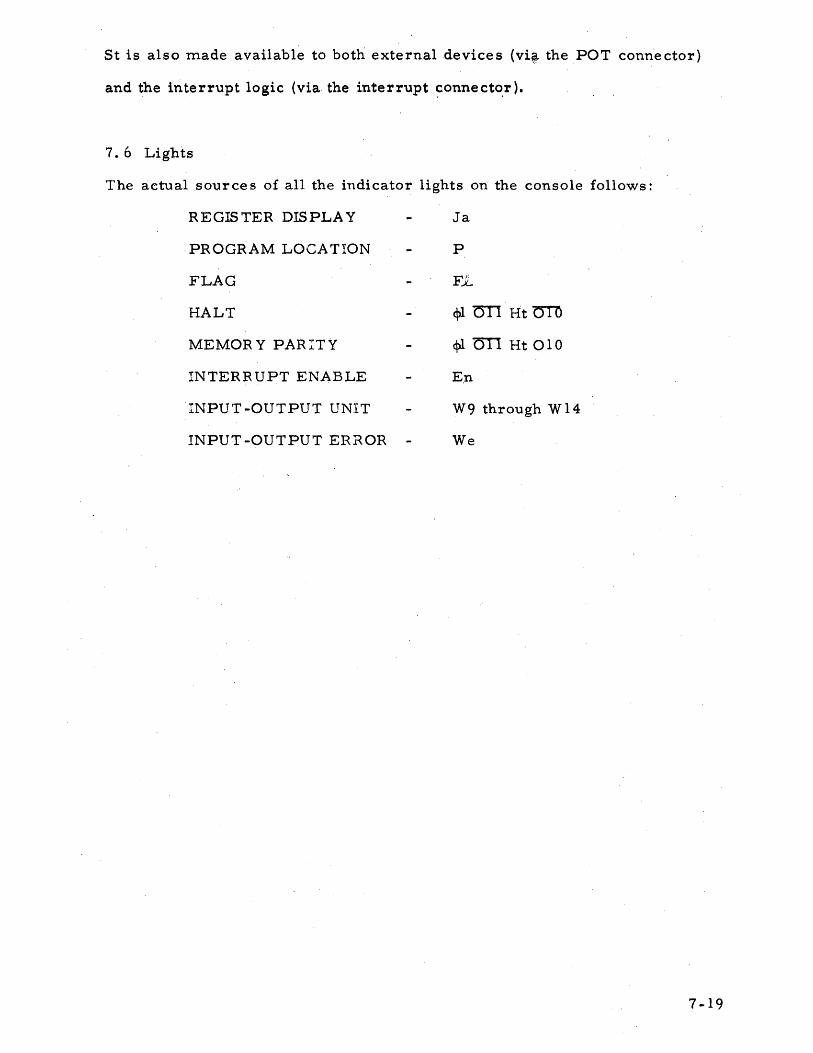
St is also made available to both external devices (vii- the POT connector)
and the interrupt logic (via the interrupt ~onnect~r).
7. 6 Lights
The actual source s of all the indicator lights on: the console follows:
REGISTER DISPLAY
,PROGRAM LOCATION
FLAG
HALT
MEMOR Y PARITY
INTERRUPT ENABLE
INPUT-OUTPUT UNIT
INPUT-OUTPUT ERROR
Ja
P
Fl.
cp1 c:m H t '()IT)
cp1 on Ht 010
E,n
W9 through W14
We
7 -19

CHAPTER 8
Int.errupts
8. 1 Introduction
8. 2 Recognition
8. 3 BR C opcode
8.4 Leaving IDLE
8. 5 Single -instruction interrupts

8. 1 Introduction
A priority interrupt level has three states:
INACTIVE
WAITING
ACTIVE
No interrupt signal has been' received into the
level and none is currently being processed by
its interrupt servicing subroutine.
An interrupt signal has been received into the
level, but is not yet being processed by its
interrupt servi'cing subroutine. (This situation
may be due to an interrupt of higher priority
being proce ssed at this time. )
An interrupt signal. has been received into the
level and is c'Urrently being processed by i.ts
interrupt servicing subroutine. This means
the' main frame has recognized the interrupt's
pre sence by exe cuting the ins tru cHon in its
assigned memory location (which is usually
a BMC, 37, to the body of its interrupt ser
vicing subrou tine).
Some flexibility is provided in the transferring bet,veen interrupt state s:
INACTIVE-WAITING Interrupt levels which do not have the
arming feature will automatically proceed
from the INACTIVE state to the WAITING
state whenever an interrupt signal is
recognized. Interrupt levels which have
the arming feature will change state s
upon r'ecognizing the interrupt signal
only if the corresponding arm is set.
If the arm is reset, no change of states
will occur and all record of the interrupt
8-1

WAITING~ACTIVE
'signal is 'lost.
Some interrupt levels will automatically
pro'ceed from the WAITING state to the
AC TIVE state if las soon as there are no
interrupts of higher priority in either the
. WAITING state or the A.CTIVE state.
Other interrupt levels will change states
only if there are no interrupts of higher
priority in the. WAITING or ACTIVE
state and the interrupt system is enabled
(i.e. En is set).
ACTIVE-"INACTIVE For those interrupt lev·els whose inter
rupt servicing subroutine consists of a
single instruction (the hardware defines
the single instruction interrupt levels by
a spe cial signal). the interrupt .level will
automatically proceed from the ACTIVE
state to the INACTIVE state at the End
of the execution of the instruction in its
as signed rnernor y lO<Ycition. For the othe r
interrupt levels, the change of states will
occur at the conclusion of the interrupt
servicing subroutine (signalled by a BR C
instruction).
E~ch interrupt level has two flip-flops (Is, Ip) to decode the three states
de$cribed above,
Is Ip => INACTIVE state
Is Ip =*WAITING state
Is Ip ~A.CTIVE state
The ~ignals from the main fram.e to the interrupt logic include:
8-2

Ti
Ie
'Ii cIo cks tL.v set of the Is flip -flop of (:~ a cll
interrupt level. Thus, the change from
the INACT~VE state to the WA ITING state
occurs on the trailing edge of Ti.
Ie cloc~the set of the Ip flip-flop associated
with the currently WAITING (Is Ip) interrupt
level of h ighe st priority .. Thu s, the chang".:
from the WA':TING state to the ACT rVE state
occurs' on the tra.iling edge of Ie.
Ib Ib clocksthe clear of both the Is and the Ip flip
flops associated with the currently ACTIVE
(Is ~p) interrupt level of highest priority. Thus,
the change from the ACTIVE state to the INACTIVE
state occurs on the trailing edge of lb.
Each of the main frame signals to the interrupt logic is normally two clock
times long
Ti TO
Ie T1
Ib Tl
=8 I ib signal only during the entering/leaving of an interrupt servicing
subroutine 0 Ti is normall y signalling during every machine cycle.
However, Ti is not allowed to drop during any machine cycle in which
Ie signals. Since it is logically impossible to enter two different
interrupt servicing subroutines on two 'consecutive machine cycles,
Ti is maxim.ally five clock time s long. This leads to: ANY EXTER NAL
INTERRUPT SIGNAL TO THE INTEHRUPT LOGIC SHOULD BE AT
LEAST 3 CYCLES LONG.
The signals from the interruptlevelsto th~_' ITlain fran'le include:
8-3
Ir
Ij
N6-N14
8.2 Recognition
and all interrupt levels of higher priority are in the
INACTIVE .state.:. . This interrupt level may proceed
to the ACTIVE state whether the interrupt system
is enabled or not.
An interrupt level is currently in the WAITING state
and all interrupt levels of higher priority are in the
INACTIVE state. This interrupt level may proceed
to the ACTIVE state only if the interrupt system is
enabled (i. e. En is set).
The currently ACTIVE interrupt level of highest
priority isa single-instruction i:q.terrupt.
The interrupt address associated with the currently
WAITING interrupt level of highest priority. These
address lines will be shifted left one binary position
to define a unique pair of memory locations.
During the End phase of most opcodes, Ir and Is are examined. If a
WAITING inter:rupt level may go ACTIVE, the next instruction is not
accessed. Instead, the instruction at the assigned memory location is
accessed and executed-with the P register still containing the address
of the ~ext instruction in the main instruction sequence. [This executed
instruction will normally be a BMC, 37, to the body of the interrupt
servicing subroutine for that interrupt level. ]
The following opcodes never allow interrupts during their End cycle:
EOM (00/40)
PO T /B PO ( 1 0/50)
WOT/ROT (11/51)
:PIN/BPI (14/54)
WIN/RIN (15/55)
BAX
BRL/BRU
(30)
(33/73) 8-4.

If the follc:>wing opcodes branch, then interrupts will not be allowed
duri:ng their End. cycle:
BDA
BFF/BFT
(70)
(31/71)
Certain conditions' will also block interrupt recognition:
1. When'STEPPING (Ks,>
2. When halting (Ht)
3. When executing the 'instruction of a single -instruction
i.nt~trupt subroutine (Ij). (If interrupts were not blo~ked)
the a\ltomatic 1b might occur after a new Ie.]
4, . When signalling a memory parity inter~upt (Cp Kpi~ [The
End Int
Tl
two tnemoryp~rity b:lterrupt signals are only one clock
time (TI) long and their falling edges will gate their
respective interrupt levels from the INACTIVE state to
the WAITING state (even though Ti remains tru.e). If>
interrupts were not blocked, this change of state might
interfere with Ie.,]
N-S
END
(Access the next· instruction from the assigned
interru.pt addre s s]
Set Ip
[Ip will block any change of P during'the next c;o.
Thus' the instruction ~t -the inter:rupt'"·address is
truly 'E~EGUTED. ]

TO
Tp
Set Ie
[Ie will gate the cU3rently WAITING interrupt level
of highes't priority to the ACTIVE state]
Do not clear Ti
[No new interrupt levels will be gated from the
INACTIVE state to the WAITING state while we
are gating this' interrupt level from the WAITING
state to the ACTIVE state (via Ie)]
Or :=;>A~:e
[~estore A and B-during operand assembly (qD),
Or caused A and B to be swapped]
M-'C (Jm)
'[i.,e. next instruction-C]
(MO-M5)-'O (Jm)
[i. e. next opcode-"'O]
M6-Lp(Jm)
[Set up Lp for cjl) J
Set Fp
[Set Fp for cjl)]
Clear Ie
[This drops the Ie signal to the interrupt logic]
Ip -=:>Set Cpe
[Check parity of the riext instruction]
'Go to qD
[Perform the next instruction]
8. 3 BR C opcode
For normal interrupt le'vels (IJ), the interrupt servicing subroutine
8-6

will control the change :trom the ACT!VEstate to the INACTIVE state.
A specialinstrnction. BRC (32). will gate (via Ib) the currently ACTIVE
interrupt level of highest prio.rity to the INACTIVE state. Unless special
programming precautions are taken; the BR C instruction should only be
used as the ~ast instruction in the interrupt servicing subroutine (i. e. the
instruction that exits from the interrupt servicing subroutine back to the
,main program). The BRC instruction has been made a 3 -cycle instructi-on
so that another interrupt may be recognized during its End ph~se.
qi1 Fp
TI
BRC
(32)
TO' cO-FL
Tp
<til Lp
T1
TO
[This loads FL from bit 0 of the first word of an
instruction (either direct or indirect)]
C1-+Pct
[This loads Pct from bit 1 of the first word of an
instruction (either direct or indirect)]
Note that this machine cycle could be concurrent with
<ji) Fpabove.
Set 011
[all will gate S to P at Tp]
Ib (through Tp)
[Ib will gate the currently ACTIVE interrupt level
of highest priority to the INACTIVE state] 8-7

Tp
Tl
.TO
Tp
Tl
TO
Tp
Oll~ S~+P (Ja, Pr)·
[i. e. effective address-+P; the branch is taken]
Ib =;::;.>Block End
[011 wQuld normally have gated End at cpo Tp.
BR C will have two extra machine cyclee to
allow the recognition of interrupts during its
End phase]
End (through Tp)
[End gates the preparation for the next instruction]
8. 4 Leaving IDLE
If a HALT instruction is executed but the RUN /IDLE/STEP switch is
left in RUN, any interrupt (En Ir + Is) will be properly processed. Upon
entering the interrupt s'ervicing subroutine, P contains the address of the
instruction following the HALT command. This usually means that, after
pro'ce s sing the interrupt, the instruction sequence will be re -entered at 8-
the instruction following the HALT comman«i.
End Ht lP
<1>1 on Ht
Tl
TO
M---C; Clear 010; Clear 011
Clear 0
[This clears out the opcode']
Clear 09
[This forces C to be displayed on the R~GISTER
DISPLA Y lights]
09~C---REGISTER DISPLAY lights (Ja, Pr)
[The REGISTER DISPLA Y lights are driven from Ja]
O~O=;>HALT light
Tem=>Mgm
(If the ~emory stack is not up to a t;n~nimum opera~ing
temperature (Tem), a memory reference will pot be
made]
Tp (jT() St Tern Kg (En Ir + ~s) ::=;, Clear Ht
<l>lorl 'Ht
[Le. Go to cpl CTI1 Ht; this is only effe'c~e4 if there is
no parity error indication (C511r), RESET is not 1;>eing
actuated (St), the memory stack temperature ism.inimal
(Tern), and the RUN/IDLE/STEP switcl1 is in RUN (Kg)]
T 1 , 'Kg =+ End (through Tp)
TO.
Tp
[End gates the preparation for the next instr'Uction
note that 0 is cleared thu s ailowing the interrupt to
always be recognized]
End::::::>Block the interchange of A and B
[End or would have gated this interchange]
8-9

End (ill + Ip) => Go to cj:O
[EXECUTE the instruction at, the interrupt addre s s]
8,5 Single .instruction interrupts
Some interrupt levels can be completely processed with one instruction
(e. g. real time clock pulse). Hardware provisions have been made to
handle these single-instruction interrupts:
1. A signal, Ij, will be held true by the interrupt logic whenever
a single-instruction interrupt level is ACTIVE.
2. Ib will be automatically sent to the interrupt logic during the
Encl pha,se 0.£ the single-instruction interrupt servicing sub
routi:~le .
3. No new interru pts will be allowed during the End phase of the
single -instruction interrupt servicing subroutine.
, Orily the following opcodes will be meaningfully interpreted as single
instruction interrupt servicing subroutine s:
EOM (00/40)
POT, PIN (10/14)
WOT, WIN (11/15)
MPO (16 )
BMC, BRM ( 37/77)
EXU (72) - Only the allowable opcode s
above may be EXECUTED
From the above, 'an earlier rule m.ay be expanded:
ANY EXTERNAL INTERRUPT SIGNAL TO THE INTERRUPT LOGIC
SHOULD BE BETWEEN 3 AND 4 CYCLES LONG.
8-10

End Ij
Tl
TO
Tp
END
Block any interrupt recognition
[End would normally have gated such recognition]
p-S
[Access the next instruction from the addr~ss in p]
Ib (through Tp)
[Ib 'will gate the currently ACTIVE interrupt level
of highest priority (i. e. the single-instruction
interrupt level) to the INACTIVE state. Note that
(since interrupt recognition at Tl time was blocked)
no other interrupt levels are currently, being gated
(via' Ie) from the V{AITING state to the ACTIVE state] . .
Ip ===;> B 10 ck Ib
[If the single -instruction interrupt subroutine is an
EXU, Ib will not be signalled until, the End of the
EXECUTED instruction]
Or~A~B
[Restore A and B-During operand assembly (<ji)),
Or caused A and B to be swapped]
M-C (Jm).
[i. e. next instruction-C]
.(MO-M5)-0 (Jm)
[i. e. next opcode -0 J
M6-Lp (Jm)
[Set 'upLp for cji)]
Set Fp
[Set 'Fp for cji)]
8-11

Clea'r 010
[Clear the memory parity error indicator -in case
a transfer to IDLEjs gated (see below)]
Clear 011
[Set up for a possible transfer to IDLE (see below)]
(Ht + Ip) ==>Set Cpe
[Check parity of the next instruction]
Go to qD
[Perform the next instruction]
Ht IP ~Go to cp1 (more precisely, <1>1 '()T1 Ht)
[IDLE -note that the HALT flip-flop, Ht, must be set
and this (Ip) must not be the End pha.se of an EXU opcode]
MPO (16) is significantly altered when executed as a single-instruction
interrupt servicing s.ubroutine. In fact, the use of MPO in this manner is
fairly well limited to the real tim.e clock pulse interrupt level.
<Ii> Lp
Tl
TO'
Tp
<P4
TI
M .... C (Jrn)
[i. e.
MPO
(16 and Ij)
operand-C]
Set Cpe
[Che ck parity of the operand]
C + l-C (J a, Pr, K 11 )
[The operand has been properly incremented]
Do not alter FJ.
[The carry out of the adder, Ku2, usually goes to F.{]
8-12

<\>7
TO
Ku2 =9- Clear Fp
[Thus Fp il1lplie'l ihatthe incremented operand now
equals 00008 (Fp was left set by ~ Lp)]
.MwCthrough Tp)
[This mernory cycle will be' a write cycle]
C"'M (Jm ... through Tp)
[The' increlnented operand will now be returned to
memory)
Fp .=>' 5 ki (throu.gh cJ>7 Tp)
[An inte~ru.pt signal is sent to the real time clock
sync inte'rru.pt level ,if the incremented, . restored
operand equ.als OOOOS]
Tl ' End (thr9u.gh Tp)
TO
Tp
[End gates the preparation for the next instruction]
8-13

CHAPTER 9
Alert and Test I/O Equipment
9. 1 Introduction
9. 2 EOM opcode
. 9.3 SES opcode

9. 1 Introduction
The ,EOM opcode s (00/40) provide one form of ou:tput from the ,main'
frame. Correspondingly, the SES opcodes (01/41) provide one form
of input to the main frame. Both EOM and SES pre sent a 16 bit control
word' (in fact, oni y the least significant 12 bits' of the control word are
presented at some I/O connectors) and various timing signals at the
, I/O conne,ct,ors.Additionally, the response.or lack of response to the , '
control word will cau.se SES'to set or clear F:.e.
The effective address (EO-EI4) ,provides 15 of the 16 bits in an EOM/SES
'control word. [~his ,effective address is'ac~ally presented from'09-011
and C.] The remaining bit is provided by the most significant bit o£ the
opcode, Or. The 16 bits of the EOM /SES control word are 1abled
GI, C9,. CIO; ••• , C22, C23
at the I/O conne ctor s. All of the above may be summ'arize d a sfollows :
Control Word Logical Source Actual Source
CI Or Or
C9 EO 09
CIO El 010
CII E2 011
C12 E3 CO
C13 E4 Cl
C14 E5 C2
CIS E6 C3
C16 E7 C4
C17 E8 C5
CI8 E9 c6
C19 ElO C7
C20 Ell C8
C21 E12 C9
C22 E13 CIO 9-1

Control Word'
C23
Logical Source
El4
Actual Source
ell
In practice, EOM's are generally used to alert an external device for an
ensuing' I/O' operation (either via the standard I/O channel or via POT /PIN);
SES's are g.enerally used to test operating states and conditions within the
external device~ .
Several general remarks may be made concerning the executiori of either
an EOM or an SES opcode:' .
1, The actual execution {i. e. pre sentation of the control word and
ti min g pul s e s} 0 c cu r s in cps.
2. The actual execution will last exactly two contiguous machine
c yele S·.
3. The C\ct~al execution v,lill start at T l Ta - and hence run through
Tp Ta.
4. The actual execution will in no way be altered by any intervening
TIMESHARE.
The above is effected by using Fp and Lp to divide <Ifi into four subphases.
Fp Lp Subphase
1 o
1 I
o 1
This is a pre -exe cution subphase that is remained
in until the first execution subphase, <Ifi Fp Lp,
may start at T 1 Ta [<ID Fp Lp is only entered if
necessary]
This is the first execution subphase"
This is the second execution subphase.
9-2

Fp
o
Lp
o
9.2 EOM opcode
The timing signals
Ql, 02
SUbphase
This is a post-executio.n subphase that is
remained in until TIMESHARE is concluded
and the next instruction may be accessed
[<j£ Fp Lp is only entered if necessary]'
are as shown below for any EOM.
'The control signal
Eom
is as shown 'below for any EOM.
One of the control signals
Buc, lac, Sys
may also be signalling, as shown below, for a given EOM (depending
on C 1, C 9, C 1 0, and C 11) •
'Ta '~l __________________ ~
cps Fp Lp J l ... ______ ---______ _
<\£ry LP ............................ ________ ---L
Q1
Q2 I Eorn I Buc
Ioc
Sys
9 ... 3

Some inte:rnal operations are effected via EOM. The as sociated control
words have been chosen so as to allow._direct scratch pad addressing.
Cl era en C17 signals one of the se internal functions. In these
cases only C 19 through C23 need be further examined:
q£) Lp
Tl
TO
Tp
C19
0'
X
X
X
X
X
1
1
C20
0
X
X
X
1
1
X
X
e21
0
0
1
1
X
X
X
X
EOM
(00/40)
C22
0
1
0
1
X
X,
X
X
(SO,..S11)-C (Ja, Pr)
C23 Function
X 'HALT
0 Clear F.i
0 Set F.J2.
0 Toggle Fi
0 Clear En
1 Set En
0 Clear Pet
1 , Set Pct
[The least significant 12 bits of the effective address
will be presented from C]
(SuO-Su2) .... (09-01l)
[The most significant 3 bits of the effective address will
be presented from 09, 010, and all]
Ta~Block the clearing of Lp
[i. e" Go to q£ Fp Lp and begin the actual execution of
the EOM]
9-4

q£) Fp Lp
Tl
TO
Tp
TO
Tp
T a :::=;> Allow Lp to cle ar
[i. e. Go to qD Fp Lp and wait o:nern.achine cy·cle before
beginning the actual execution of the EOMI
Ta~Set Lp
. [i. e. Go to qD Fp Lp and begin the actual execution
of the EOM]
Eorn (through qD Fp LpTp)
[This control signal is not gated by any special EOM
control word( s)]
Eorn. cr CTIT CIT::::>Buc (through qD Fp Lp Tp)
[Internally this is equivalent·to Eorn. Or crnJ on]
01 (through ctD FP Lp'TO)
[This tirn.ing signal is !lot ga.-ted by any special opcode(s)]
02 (through ctDFP Lp Tl)
[This tirn.ing signal is not gated by any special opcode(s).]
Eorn. C 1 CIa Cll:::::>Ioc (thi"ough q£) FpLp TO)
[Internally this is equivalent toEorn. Or 010011]
Clear Fp
[i;e.Go to 46Jp Lp, where the actual execution of
the EOM is concluded] ,~ ,
-Eorn. ~ 'CIO Cll~Sys (throughq£) Fp LpTO)
{Internally this is equivalent to Eorn. 09 010 011]
9-5

TO
Tp
q£) E:P Lp
fp Tsq =-End (through Tp)
[End gates the preparation for the next instruction
if a TIMESHARE is not about to begin (Tsq) and. this
is not theautomat.ic EOM of a: FILL operation (iP)]
Block any interrupt recognition
[End wou.ld normally have gated such recognition]
(q£) Tp End rp Ts)=;>FILL~558-0
Ts :$ClearLp
[1. e. R IN -0 ]
Set Fp
[This initializes Fp for cp2]
Clear Lp
[This initializes Lp for cpz]
Clear Ip
[This initialize s Ip for the End of RIN]
Go to <jl2
[The R IN opcode sequence is.
entered at <jl2]
[i. e. Go to cjD 1P Lp to await the conclusion of TIMESHARE]
Ti· Ip Tsq ~End (through Tp)
TO
[End gates the preparation for the next instruction
if a TIMESHARE is not about to begin {"TS"Ci'} and this
is not the automatic EOM oia FILL operation (IPl]
lUock any interrupt recognition
[End would normally have gated such recognition]
9-6

---Tp (<t>5 Tp End Fp Ts)==>FILL~558"'O
[i.~. RIN-+O]
Set Fp
[This initializes Fp for cpzl
Leave Lp clear
[This initializes Lp for 4>2]
Clear Ip
[This initializes Ip for the End
of RIN]
G'.I to $2
[The RIN opcode sequence is
entered a,t cp2]
Ts .... Do nothing
[i, e. Renlain in cp5 FP Lp awaiting the conclusion
of TIMESHARE]
9. 3 SES opcode
The timing signals
01, 02
are as shown below for any SES.
The control signal
Skss
is as sho'wn below. However, note that the re are two pas sible tirrlings-
depending upon C9 of the SES control word. The response to the control
word (this response is stored in FX) may come, externally, from either of
Sio, Sse
depending on C 1, C 9, C 1 0 and C 11 .
9-7

Ta
Qf) Fp Lp. ___ .....
qD Tp Lp. ...... ' _________ --..1
Q'l
02 I,
Skss" C9 --.....
Tp TI TO Tp TI TO Tp Tl
9-8

Some internal tests are made via SE5. The associated control words have
been chosen so as to allow direct scratch pad addressing. Cl C9 ClO Cli C1"7
" signal s one of these internal tests. In these cases only C19 through
C23 need be further exanlined:
<pO Lp
Tl
TO
Tp'
Cl9 C20 C21 C2l C23 Test
X X I 0 0 BREA,KPOINT # 1 (Kbl-+Fl)
X X I 0 I BREA,KPOINT #2 (Kb2-+F.RJ
X X 1 1 0 BREA.KPOINT #3 (Kb3-+F1.)
X X 1 1 1 BREAKPOINT #4 (Kb4-+F,Q)
X I X, X X Interrupt enable (En-+F,()
1 X X X X Program controlled trap (Pct-+F)J
SES
(01/41)
(50-511 )-+C (Ja, Pr)
[The least signific'ant 12 bits of the effective address
will be presented from C]
(SuO-Su2)-+(09-01l)
[The most significant 3 bits of the effective address
will be presented from 09, 010, and all]
Ta~Block the clearing of Lp.
[i. e. Go to cpS Fp Lp and begin the actual execution
of the SES]
Ta~Allow Lp to clear
[i. e. Go to cp5 Fp Lp and wait one nlachine cycle before
beginning the actual execution 6£ the SESJ
9-9

cps Fp Lp
Tl
TO
Tp Ta ::::::>Set Lp
cps Fp Lp
[1. e. Go to cj£ Fp Lp and be gin the actual exe cution
of the SES]
Tl C9 ~Sk.ss (through q:6 FP'Lp Tp)
[Internally this is equivalent to C59]
TO Q 1 (through <f:6 FP Lp TO)
[This timing signal isnot gated by any special opcode(s)]
02 (through q:6 Fp Lp T 1)
[This timing signal is not gated by any special opcode(s)]
Tp Clear Fp'
cps Fp Lp
[1. e. Go to qs Fp Lp J whe re the actu.al exe cution of the
SES is concluded]
T 1 ' C9 =+Skss (through cj£ Fp Lp Tp')
TO
[Internally this is ,equ.ivalent to 09]
Tsq~End (through Tp)
, [End gates the preparation for the next instruction
if a TIMESHARE is not about to begin (Tsq)]
Tp $es-..Fl.
[Se s iS t logical! y J the re sponse to the SES control word]
Ts ~C1ear Lp
[i. e~ Go to cj£ Fp Lp to await the conclusion of
TIMESHARE]
9-10

cp5 Fp LP"
Tl
TO
Tp
Tsq~End(through Tp)
[End gat~s the preparation for the next instructi~n
if a TIMESHARE is not about to begin (Tsq)]
Ts =::!;>Do nothing
[i. e. Remain in <l>5Fp Lp awaiting the conclusion
of TIMESHARE]
9-11

CHA.PTER 10
Parallel I/O
10. 1 Introduction
10.2 Connectors
10.3 POT/BPO opcode
10. 4 PIN/BPI opcode

10. 1 Intr'oduction
Th~re are two independent I/O' paths on ,all 92 comput~rs:
1. Standard 1/0 Channel
a. Cha'racter I/O
b. ' ~uffered
c. ' Oriented towards stanc;lard peripherals
2. POT/PIN'
a. Full word I/O
b. Unbuffered
c. Oriented towards systems application,s
. This chapter is ~onc.erned with the POT /PIN system. The POT
(parallel, output) operation is very similar to the' PIN (parallel input)
operation; hence the two operatio~s wi.11 be discussed simultaneously.
The actual execution of the POT /PIN oc~urs during .~2. The logic will
hang up in cpZ'waiting fora READY Signal from, the external equit:>ment.
Upon 'receiving the READY signal, the nlain frame will send a reply
(Pot2/Pin)~ If this is a POT, operation', the output word will be avail
able at the output connector (G1Z through C23) while Pot2 is true. If
this is a PIN operation, the input word will be sampled at the input
conQ,ector (Cd12 through Cd23) on the trailing edge of Pin.
There are two speeds of POT/PIN available. There are two possible
READY, signals (Rt and Rtf) from the external equipment to the main
frame. The external equipment will select the, high speed mode (Rtf)
or the low speed mode (Rt) by the REA,DYsignal which it sends.
HIGH SPEED MODE'
Rtf causes 010 to set at any T1 time. 010 then gates the execution of a,
POT /PIN, operati<?n in one machine cycle. The timing of the pertinent
signals is: 10-1

010
Ta
Lp
01
Tp Tl TO Tp Tl TO
L OW SPEED· MODE
Rt causes Lp to set at any Tl Tatime. Lp then gates the execution of a
POT/PIN operation in two machine cycles; naturaily this execution will
not be a~tered in any way by an intervening TIMESHA.RE. The timing of
the pertinent signal~ is:
QZ .1 _________________ _
Tp Tl TO Tp Tl TO Tp Tl
10-2

The POT (10) and PIN (14) opcodes b"'~re the block .transfer equivalents
BP.O (50) and BPI (54). The logi-c stays. in tP2 throughout the block
transfer. As each word in the block is transferred, the A registe.r
will be decrelnented by one. The block transfer is terminated either
by program control (the A registe14 decrernents through zero - thus
. the original contents of A. equaled the block length minus one) or by
external control (the external equipment signals BLOCK TERMINA.TE,
Bt), In the high speed nlode, BPO/ brl Inay (depending on Rtf) transfer
a word every machine cycle. IXl the low speed "mode, BPO/BPI may.
(depending on Rt) transfer a word every tw'O machine cycles .
. A POT (BPO) uperation provides one additional signal, Potl, which
is true as long as the logic reITlains in <1>2. A. PIN (BPI) operation
provides one additional pulse, Rti, 'which is true for two clock times
when the logic leaves 'cj>2.
Some of the general purpose flip-flops used in cp2 of the execution of
POT/BPO and PIN/BPI include:
Fp During BPO operations Fp' gates the next output
word into C, the parity checking of this new output
word, arid the incrementing of S so that the following
word in the output block may be accessed.
Durirg BPI operations Fp gates the incrementing of
S so that the current input word may be stored into._
the next word of the input block.
Lp Lp will gate the transfer of one word in the low
speed mode (Rt).
09 09 gates the termination of POT/BPO or PIN/BPI.
(1. e. 09 gates the exit from cj>2) .. 09 may be
set because:
10-3

1. A. word has. been transferred and the
. oper~tion was .not a block transfer
(i. e. the opcode was POT or PIN)
2. All words in the defined block have
been transferred (i. e. A has been
decremented to 7777 8)
3. The exte rnal device has signalled the
end of the block (via Bt)
010 010 will gate the transfer of one word in the high
speed mode (Rtf).
all puring BPI operations 01T signals that the last
input word has been stored in memory.
10.2 Connectors
Following are the logic signals on the POT /PIN connectors. Note also
the many EOM/SES signals on these connectors.
POT PIN CONNECTOR CONNECTOR
1. Potl Pin L.
2. Pot2 2.
3. Ioc Sio 3.
4 •. Buc 4.
5. Sys 5.
6. Earn 6.
7. QI. 7.
8. QZ Rti 8.
9. lftT Rtf 9.
10. Rti 10.
10-4

CONl'-.fEC; TOR CONNECTOR
11-. Bt 11.
12. Q2 12.
13. Skss Skss 13.
14. Sio· 14.
15 .. sse 'SSc' 15.
16. Rt lIT 16 ..
17. St 17.
18. Cl7 m 18.
19. . 19.
20. 20.
21. CI 21.
2Z. 22.
23. 23 •.
24. 24.
25. 25.
26. 26.
27 ;. 27.
28. 28.
29. C9 29.
30 CIO 30.
31. CII 31.
32. C12 CdI2 32
33. CI3 Cd13 33.
34. C14 Cdl4 34.
35. CIS CdI5 35.
36. CI6 Cdl6 36.
37. C17 Cdl7 37.
38. Cl8 Cd18 38.
10-5
POT PIN CONNECTOR CONNECT,OR
39. C19 Cd19 39.
40. C20 Cd20 40. '
41. C21 Cd21 41.
'42. - C22 Cd22 42.
43. _ C23 Cd23 43.
10.3 POT/BPO opcodes
<pO Lp
TI
TO
Tp
Tl
POT/BPO - LOW SPEED
(10/50)
Set Cpe
[Check parity of the first output word]
NOTE: Fp is set; 09, 010, 011, and Lp are cleared;
Go to cj>2 Ta or <{l2 Ta - depending on Ta.
Pot! (through cj>2)
[Potl is true throughout a POT/BPO operation]
Fp TS=!!>M:+C (Jm)
[This takes -the next (first) output word to C]
S + I ....... S (Ja, Pr, Kll)
[Thus the following word in the output block will
be accessed]
Cle~r Fp
[The logic is now ready to output a word from C]
10-6

TO
Tp
<1>2 Ta
T1
Rt'09 (rp + TS)~Set Lp
[The low spee'd ~EADY signal, Rt, will be' recognized
if th~ logiG is not gated to terminate the output' (C5.9)
and either the C register already has the next output
word (Fp) or this next output word is currently being
gate d to C (TaT]
Lp =;>PotZ (t~rough TO Ta)
[PotZ indicates, to the external equipment, that the
data lines (C12-C23) may be strobed]
Lp BPO ~A, .. l-+A, (Ja, Gn, Pr)
[A, is decremented by one as each word is transmitted]
Lp 'RU2 => Set 09
[The POT I BPO ope'ration will be concluded following
'th£s transmission either, because it was a single ~ord
transmission (POT :::::> KuZ) or because the ']j'PO ·block
len,gth has been reached (decremented A = 77,77 8~''R\i"2). ]
Fp 09 TS ~ Set Cpe
[Check parity of the next word in the block]
(09 + Lp) ~Stay in <1>2
[The transmis sion is not co,mpleted]
09 Lp =>Go to <\>7
[The transmission is complete]
Fp Ts =>M-+C
[This takes the next (first) output word to C]
s + 1-+-5 (Ja, Pr, K11)
[Thus the following word in the output blo~k will be
accessed]
Clear Fp
[The logic is now ready to output a word frOm C]
10-7

TO
Tp
Tl
TO
Tp
cpO Lp
Tl
TO
Tp
Lp==>Set Fp
[Fp gates the, prep~ration for the next output word]
Clear Lp
[This concludes the transmission of a data word]
Fp 159 TS::::;> Set Cpe
[Check parity of the next word in the block]
'm ~Stay in cp2
[The transmission is not completed]
09 => Go to <1>7
[The tr'ansmis sian is complete]
End (through Tp)
[End gates the preparation for the next instruction]
Block any interrupt recognition
[End would norm.ally have gated such recognition]
POT /BPO - HIGH SPEED
(10/50)
Set Cpe
[Check parity of the first output word]
NOTE: ,Fpis set; 09, 010, 011, and Lp are cleared
Pot 1 (thr ough cp2)
[Potl is true throughout a POT / BPO operation]
10-8

Tl
TO
Tp
Fp Ts =>M"'C (Jrn)
[This takes the next (first) output word to cl S + 1-.s (Ja, Pr, Kll)
[Thus the following word in the (possible) output block
will be accessed]
Clear Fp
[The logic is now r'eady to output aword from. CJ
Clear 010
[This concludes the transmission of a data word]
Rtf '09 Tsq ~Set 010
[The high speed REA.DY signal, Rtf, will be recognized
if the logic is not gated to terminate the output ('09) and,
the next word in the (possible) block may be accessed at
the conctusion of this word transmis sion ("T"SVl
010 =9Pot2 (through Tp) ,
[Pot2 indicate s, to the exte rnai equipment, that the '
data lines (C12-C23) may be strobed]
Set Fp
[Fp gates the pr~paration for the next output word]
010 BPO :::::::.>A.-l-+A (Ja, Gn, Pr)
[A is decrem.ented by one as each word is transmitted]
010 Ku2 ==:> Set 09
[The POT I BPO operation will be concluded following
this transm.ission either because it was a single.
word transmission (POT ~'Ku2) or because the BFO
block length has been reached (decremented A
Ku2)]
'09 010 Ku2 ~Set Cpe
[Check parity of the next word in the block]
..
10 ... 9

cp7
(09 + 01 0) ~Stay in q)2
[The transmissio~ is not completed]
09 oro ~Go to c\>7
[The transmis sion is complete]
Tl . End (through Tp)
TO
Tp
(End gates the preparation for the next instruction]
Block any interrupt recognition
[End would· normally have gated such rec~gnition]
10. 4 PIN / BPI opcode s
. ~ Lp
Tl
TO
PIN /BPI - LOW SPEED
(14/54) .
Tp NOTE: Fp is set; 09,010,011, and Lp are cleared; Go
to ~ Ta or ~ Ta - depending on Ta.
~ Ta Mw
[Every m.emory cycle in ~ will be a write cycle]
C-M (Jin)
[The input word in C will be written into m.emory J
T 1 R t 09 (011 + T s q) ~ S et Lp
[The low speed READY signal, R t, will be recognized
if the logic is not gated to term.inate the output (09) and
either the previous input word has already been stored
in memory (OIT) or this previous input word may be
stored during the ensuing mem.ory reference (Tsq). ]
10-10

TO
Tp
4>2 Ta
Tl
Lp :::::;> Pin (through TO Ta)
[Pin indicate s, to the exte rnal equiprnent, that the
data lines (Ccl12-Cd23) will be strobed (on the t,railing
'edge of Pin)]
"TS~Clear 011
[The current memory reference is storing the last
input word]
Lp BPI ·=;'A,-l"'A, (Ja, Gn, Pr)
[A, is decrenlented by one as each word is transmitted]
Lp Ku2 ::.~Set 09
[The PIN/BPI ope ration' will be concluded following
this transmission either because it was a single word
transmission (PIN ,~Ku2) or because the BPI block
length has been reached {decremented A = 7777 8 ~ "RU!J]
(09 + Lp) ~ Stay in </>2
[The transrnis sian is not completed]
09 Lp ~ Go to </>4
[The transmission is complete]
Mw
[Every memory cycle in cp2 will be a write cycle]
C ... M (Jm)
[The input word in C will be writte'n into memory]
Lp FP ~S + l"'S (Ja, Pr, Kl1)
[The address within the data block is incremented to
store the currently incoming data word]
Lp -=>C,1ear Fp
[FP gates the incren1.ent of S (see above) before
stOring every input word except the first one]
10-11

TO
Tp
T1
TO
Tp
<1>7
Tl
Lp~Cd-+C
[The input word is gated into C]
Ts Lp ~Clear all
[The currentnlemory reference is storing the last
input word]
Lp =:> Set all
[A. new input word has been gated into C and must
be stored in rrlemory - the current memory reference
is storing unpredictable results since C was changed
in the middle of the memory cycle]
Clear .Lp
[This concludes the transmission of a data word]
09 ~Stay in cj>2
[The transmission is not' completed]
09~Go to cp4
[The transn'lission is complete]
C-+C (Ja, Pr)
[This is a hardware quirk]
Mw (through Tp)
[This memory cycle will be a write cycle]
C-+M(Jm-through Tp)
[The last input word will be written into memory]
Rti (through Tp)
[R ti indicate s, to the exte rnal equipment, the completion
of a PIN/BPI operation]
End (through Tp)
[End gates the preparation for the next instruction]
10-12

TO
Tp
cpO. Lp
Tl
TO
Tp
Tl
Block any interrupt recognition
[End w.ould normally have ga~ed such recognition]
PIN/BPI - HIGH SPEED
( 14(54)
NOTE: Fp is set; 09, 010, all, and Lp are cleared.
Mw
[Every memory cycle in 4>2 will be a write cycle]
C-..M· (Jm)
[The input word in C will be written into m.em.ory]
010 Fp =>5 + 1-..5 (Ja, Pr, K11)
[The address within the data block is incremented to
store the newly strobed input word]
. 010 ~Clear Fp
[Fp gates the increment of 5 (se.e above) before
storing every input word except the first one]
Clear 010
[This concludes the transmission of a data word]
R·tfm Tsq~SetOl0
[The high speed READY signal, Rtf, will be recognized
if the logic is not gated to te rrninate the output ('09Y
and the previous input word m.ay be stored during
the ensuing m.em.ory reference (Tsq)]
10-13

TO
Tp
Tl
TO
Tp
010 ::::;:'Pin (through Tp)
[Pin indicates, to the external equipment, that the
data lines {Cd12-Cd23} will be strobed (on the trailing
edge of Pin)]
010 =>Cd .... C
[The input word is gated into CJ
010 BPI ~A-l~A. {Ja, Gn, Pr}
[A. is decremented by one as each word" is transmitted]
010 Ku2 ~Set 09
[The PIN! BPI operation will be concluded following
this transrnission either because it was a single word
transmission {PIN~Ku2} or because the BPI block
length has been reached (decremented A = 7777 8~
Ku2)]
"(09 + 01 O) ~ Stay in <1>2
[The transmis sion is not completed]
09 010 =>Go to <1>4
[The transmission is complete]
C .... C (Ja, Pr)
[This is a hardware quirk]
Mw (through Tp)
[This memory cycle will be a write cycle]
C .... M (Jm-through Tp)
[The last input word is {unnecessarily} re-written
into memory]
Rti (through Tp)
[Rti indicates, to the external equipment, the
completion of a PIN/BPI operation]
10-14

4>7
. Tl
TO
Tp
End (through Tp)
[End gates the preparation for the next instructi~n 1 Block any interrupt recognition
[End would normally ha.ve gated such recognition]
10;...15

CHAPTER 11
Standard I/O Channel
11 . 1 Initialization
11.2 Character transmission and precessing
i 1.3 Parity
11.4 Channel error
11. 5 Te rrnination
11 . 6 Channel te sts
11. 7 Interrupts
11.8 Mag-tape. SCA.N
11.9 Interlace
11. 10 Connectors
11 . 11 Channel timing charts
11. 12 Channel opcode s
11.13 WOT IROT opcodes
11.14 WIN/RIN opcodes .

11 . 1 Initialization
The standard I/O channel operates, basically, in the following manner .
. A. buffer control (Cl era CII ::::;.Buc) EOM with Cl7 true 'will initialize
both the channel arid the selected peripheral for an I/O operation.' The
initializing of the channel is perfo.rmed in two stage s:
1. Wc clears the channel
2. 'We gates the set-up of the channel. according to the EOM
control word:
a. C13 is examined on output ope rations to determine
if leader is desired. C13 gates leader-basically
. by forcing an all-zero ·(including zero parity)
output character before transnlitting the prograrn
defined output characters.
h. GI6, which defines Z character/word m.ode, is
"permanently" stored in Wt and used to initialize
the character counter, W8.
c. CI8-CZ3 are stored in the unit address register,
W9-WI4. Note that the rtlost significant bit of
the unit address defines the direction of the
transmission (i. e. C18 = W9·~ INPUT; CI8 = W9·~
OUTPUT).
11. Z Character transnlission and precessing
After initialization the transmission of I/O characters may begin:
The channel contains a 12-bit buffer register, ·WrO-Wrll, and a 12-bit
character register, RI-RI2. All input characters are strobed from the
input character lines, Zwl-Zw12, into·R. All output characters are
presented to the output character lines, Rwl-RwlZ, fronl R. The Wr
register acts as a one word buffer between the nlain frarne and the
11.1
peripheral. During input operations, characters are assembled in Wr
until thedefin~d computer word is complete (1 o~ 2 characters/word) .
. Wfsignals that Wr is full. The main frame nlust then store this word
in memory; meanwhile, however, 1he channel could be strobing another
input character intoR .. During output operations, characters .are dis-.
assembled from Wr until the defined computer word is exausted (1 or 2
characte~s lword). Wl signals that. Wr is elllpty. The main frame must
then load Wr with another wordfrom .rr.Lemory; meanwhile, however, the
. channel is presenting the last, disassembled output character from. R.
·The· actual transr.niss.ion of I/O characters is controlled by character
clocks ,Ecw, from the peripherals. The character clock is syncronized
(and voltage spikes eliminated) within the channel by two flip-flops, W6
W6W5 The channel is awaiting a character clock.
If this is an output operation, a character
is currently being presented on the output
lines (from R)
W6 W5 The channel has recognized the character
clock. If this is an output operation, a
character is currently being presented on ,
the output lines (from R). If this is an
input operation, the input lines are being
strobed (into R)
W6 W5 The channel has recognized the dropping
of the character chck. If this is an output
operation,. the channel is attempting to
disassemble the next output character
(from Wr) for presentatiori (the current
contents of the output li.ne s are unpredictable).
11-2

W6W5
If this is an input opera;tion, the channel is
attempting to as se;mble the just- received
input character (into W'r) fi
If this disassembly/ assembly can be,
effected (Wf) the' channel will return to
the m W5 state.
The channel could not effect a dis'assembly/
assen1bly (W1). The channel must wait, in
this state, until the main frame presents
(to Wr) a new data word (for the output
operation) or ,stores (from Wr) the 'assembled
data w~rd (from the input operation)., This
action by the main frame (signalled by Wx)
will then allow the disassembly/ assembly to
be effected (Wx will set Wf) and the channel
will return to the Wb W'"s state. [During output
operations, all output line s (including parity)
will be held clear while the channel remains
in this, state. ]
The disassem,bly/ assembly of characters between Wr and R has been giv,en
a spe·cial name, precessing. Precessing is gated by W4. Precessing is
accomplished by an interchange of Wr and R. The actual interchange effect
ed depends on the operation (input or output) being performed.
During input operations, precessing gates the following shift paths:
0 Wr 5 f:::J 6 Wr 11
D I
<J 1 R 6 7 R 12
11-3

where the 1 character /word mode must always effect two precessing
steps (on two contiguous clock times).
During output ope rations, pre ces sing gate s the following shift paths:
o Wr5 6 Wr 11
1 R 6 7 R 12
where there is no difference between the 1 character/word mode and the
2 character/word mode.
Like most other I/O operations, two machine cycles are (rr:Linimally)
needed to complete one character transmission. The timing of the
pe'rtinentsignals is: ,
Ta'
01
02
Ecw .~ """-----__ ~I W6
W5
Tp T1 TO Tp T1 TO Tp T1
11-4
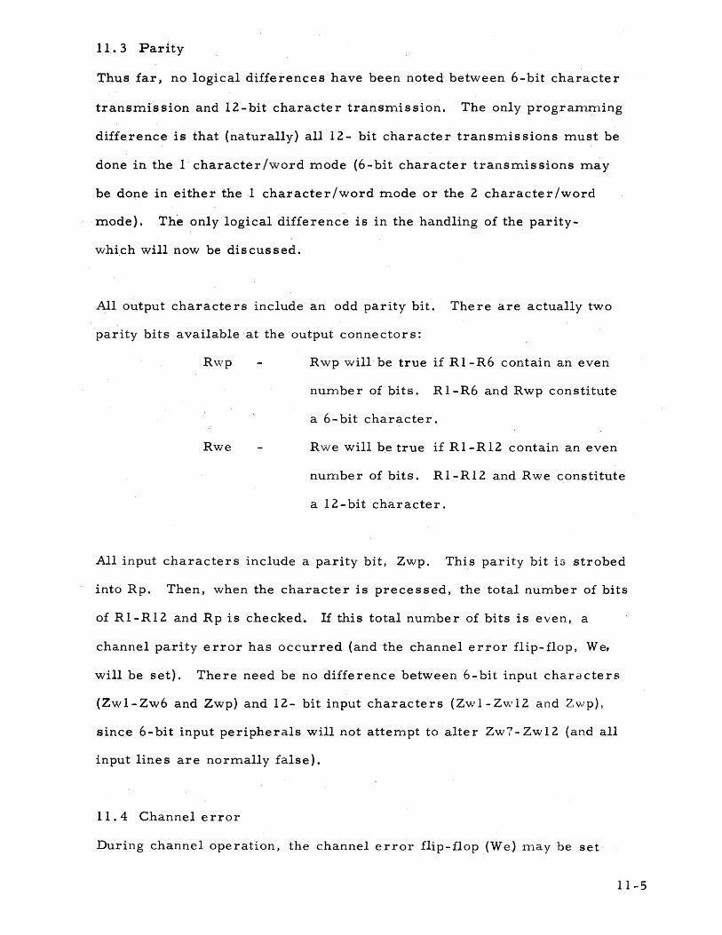
11. 3 Parity
Thus far, no logical differences have be'en noted between 6-bit character
transmission and 12-bit character transmission. The only progranlnling
difference is that (naturally) all 12- bit character transmissions must be
done in the I character/word mode (6-bit character transmissions rrlCiy
be done in either the ,1 character/word mode or the 2 character/word
mode). The only logical difference is in the handling of th~ parity
which will now be discussed.
All output characte rs include an odd parity bit. There are actually two
parity bits available 'at the output connectors:
Rwp Rwp will be true if R1-R6 contain an even
nun1be r of bits. R l-R6 and Rwp constitute
a 6- bit character.
Rwe Rwe will b,e true if R1-RI2 contain an even
nUITlber of bits. RI-R12 and Rwe constitute
a 12-bit character.
All input characters include a parity bit, Zwp. This parity bit is strobed
into Rp. Then, when the character is precessed, the total number of bits
of R1-R12 and Rp is checked. If this total number of bits is even, a
channel parity error has occurred (and the channel error flip-flop, We,
will be set). There need be no difference between 6-bit input characters
(ZwI-Zw6 and Zwp) and 12- bit input characters (Zv/I-Zw12 and Zwp),
since 6-bit input peripherals will not attempt to alter Zw7-Zw12 (and all
input lines are normally false).
II . 4 Channel error
During channel operation, the channel error flip-flop (We) ITlay be set
11-5

in three possible way:
1.. The peripheral can detect an error and signal the channel
{viaWes} .
2. The channel can detect a parity error in an input character,
. [The peripheral can signal the channel (via Np) to delete the
parity checking of input characters.]
3. The channel can detect a RATE error if an incorning character·
. clock {Ecw TO Ta} can not be processed {because the channel
is in the Wb W5 state}.
11 . 5 Termination
An I/O channel operation n1.ay be terminated by the peripheral. The
peripheral halt signal, Whs, is received in the channel halt flip-flop,
Who Wh will then gate a disconnect {i. e. the unit address will be
cleared-no peripheral will have a unit address of 008} and the I/O
operation is corDpleted-as far as the peripheral is concerned. The
n'lain fran1.e may still have input characters (in Wr~ and even R) to
store in memory.
During a paper tape input operation, the I/O channel actually generates
the halt signal, Wph. Wph will also set Wh and the termination of the
operation will be as above. This paper tape halt signal, Wph, is gen
erated when an all-zero input character (including zero parity) is
received into R. This all-zero, halt character is not further treated
as an input character (i. e. unlike the meaningful data characters, it
will not be precessed into Wr).
An I/O channel operation may also be terminated by program. An
input/output control ('C1 'CTn C 11 ~ Ioc) EOM vv'ith
11-6

C13 = 1
C17 = 1
C19 = 0
C20 = 0
C21 = 0
e22 = 0
C23 = ·0
will effect this program termination (TIP ~Terminate input;
TOP =9Terminate output)
During the init ialization for an input operation, the terminate input flip
flop (Wtr) was cleared. When the program terminates an input ope:ration,
Wb: will be set.' Wtr will hold Wf set. This means that the Wr register
will never again appear "full". Input characters will be received normally.
But these characters will be shuffled through· Wr and lost; the main frame
will not be gated to store anymore data words.· When a halt signal (Whs or
Wph) sets Wh, the channel will conclude' its ope ration normally.
During the initialization for. an output operation. the terminate output flip
flop (WO) was set. When the program terminates an output operation, WO.
will be. cleared. When the .last remaining character in Wr has been trans. ...
mitted, the channel will enter the Wb W5 WO state. If the channel is not
doing a mag-tape operation, the m W5 WQ state will directly' ~et Wha,nd
the channel will conclude its operation· normally. If the channel is doing a
mag;,..tape operation, the channel will remain. in the m W5 'W'O state until
the m.ag-tape,,·sets Wh (viaWhs).. The channel will then conclude its op
eration normally. [The WO flip-flop has a different function during input
operations. WO is cle·ared during the initialization for an input operation.
11-7

WO will be set (and remain set) when one computer word of input
characters (lor 2 characters as defined in the initializing EOM)
has been received (in R) by the channel..J
All termination sequences (both input and output - both peripheral
initiated and program initiated) will clear WO at some time in the
sequence. , we gates the conclusion of any termination sequence:
1. WO will block any TIMESHARE requests by the interlace
logic.
2. WO will block any Ilw interrupt signals.
3. W1f will block any action by a WOT fROT or WIN fRIN opcode.
4. WlJ will gate the I2winterrupt signal (which must be' 2 cycles
long, since Ti may remain true throughout anyone given cycle).
11.6 Channel te sts
Two conditions in the channel may be program. tested. A buffer control
(C1 C9 cro CTI) SESwith C17 true will effect these test:
1. The channel error flip-flop, W'e, is tested by also having C2
true. Then
We~Set Fl
We==:;. Clear F~
2. The current operating condition of the channel (ACTIVE or
,INACTIVE) is tested by also having CO true. Then
INACTIVE ~Set Fi
ACTIVE ==;>Clear Fl
The channel is INACTIYE only if the unit address is clear (i. e. W9-
W 14 = OOS) and no inpu~ cha.racters are remaining to be stored following
the termination of an input operation.
11-8

11. 7 Interrupts
Two .interrupt levels, with arms , are available for use in conjunction
with an rio operation.
The Ilw interrupt (armed by setting Aiwl) signals that the Wr registe~.
is full (during input operations) or empty (during output operations).
The 12w interrupt (armed by setting Aiw2) signals that the channel
has. gone from the ACTIVE state to the INACTIVE state.
These interrupts .are .armed and disarmed by an input/output control
(Cl CTO Cll.:::::::;.Ioc) EOM with
C14 = 1
C17 = 1
Cl9 = 0
C20 = 0
C21 = 0
e22 -= 0
C23 = 0
C 15 will be copied into Aiw2; Cl6 will be copied into Aiwl.
11. 8 Mag-tape SCAN
The rio channel participates in the execution of one, very special
periphe·ral function: A mag-tape SCAN. When SCANNING, Wf 'is
blocked from re setting. This means that input character s are re
ceived normally into R but are shuffled through Wr and lost. The
main frame will not be· gate~ to store any input words. When the
tape unit reaches the end of the tape record, the mag-tape gap signal
(Mtg) will become true. This will force Wf to clear. The main frame
11-9

is now gated to store a data \Nord (the last two characters in the tape
record). [An Ilw interrupt will also (if armed) be generated when
Mtg. clear s W£' ]
SCANNING is only allowed in the 2 character /v..;ord mode. The character
counter, W8, has long since gone to zero (W8) vvhen Mtg first becomes,
trueo When the main frame store s the data word (the Last two characters
in the tape record), the character count will be reinitialized (this nleans~
in the 2 character /word mode, that W8 will be set). W8 will be used to
blockMtg (which is still true) from again clearing Wf. [If Wf were ag2in
cleared, another Ilw interrupt would be generated (if armed). ]
A mag-tape READ operation may be converted to a SCAN operation at any
point in the tape block. This change is effected by an input/output control
(eI era C 11 ==;Ioc) EOM with
11. 9 Interl ace
C 12 = 1
C 17 = 1
C19 = c
C20 = 0
C21 = 0
C22 = 0
C23 = 0
An interlace option is available for the I/O channel. Basically, the interlace
will automatically service Wr {when Wf clears} by directly referencing'mem
ory (via TIMESHARE). During output operations, M will be gated directly to
Wr (via Jm). During input operations, Wr will be gated directly to M (via Jm).
The address of the memory reference is given by the Iwa register
11-10
in the interlace ·l~gic.. The lnte.rbice also has a' block length regi • ..,r,.
Iwl .. After ea'ch interlaeemem(>~y :refe;rence(signalled. by the ·traU';' . . .' - ',' "
ing edge ofDmc Tsl, the interl~cewill inc.rement Iwa byona and .
de crement Iwl by one. [Note that the interlace will never TIMESRAR~,
two contiguo~ s rnemor y-,ey~+, .. ii~b~JA~~1~9~.,;1~I~~,.vdl~.).,\,at~;:,~~s'iQ~ . =::: '" '. ';: ,: ",'(':.,'& v"'::';">" i"~~I .. :,,~~... f .. "~.\~.; .. ;::,'.~~'''''' ',:. ,:,;: >:- : .. ~ ' ...... ',- . ~l;'.~'·'.J . '. '. ;>:'~:./.} .. :. "'~":'.> :':{ ... ','.; -, .' :"".' -:. .'. ~:"'.: ;
Wf t~o late in' the TIME~AREf>,me~Qry c:yc:le ~o;t: ~y'p~e~e.sinl. dU:~li~'(; . that rrtemory cycle). Th\l.s tbe~.1tit~rla,~en1ayp~rfQ;tn. theincr'emenJJlLna)
de crement at leisure.' ~
The interlace informs t1\f:"ina~n frame' of its cu;rl."trdt .. trt.i~ JJy threeai,"'.l.: " :"1" \ ,... .. , .. :;",'" ,',
1. Ewl + EwZ ... , .
2 .. " Iw
3. . Iwf
. . .
01" i'~ in the pro~s~of reeel .. ingthe·
starting a6dr :'<9,><lwa}Ud\lle biltck , .' ~ \;~' .-.:' ""., . ~', ... . .
,thi$ i8 actually th.
b~<>ck l,ength ~~$.'()n~}~
'[The interl~cf, i • • 1~"~4 .fo~ th •• : ."I~·:.;-'>·\ .' ",' .... .... . . ...... ,...'.,:',:'i," '.' . \::"i}', :\:,·,i.:'; .
up by any bixf£ereoatrof:(e1 :l!t1:,:~'('i~~~' . ':-,,' ...•........ . >.,., , .' " ,<:,:,\;,;;·<·.:*:,'i"
Buer~r inPut/OU~\U;Q"c)l(C1'~;"::1 =+
'. IoelEOMWl1~~~h:.~£y. T)le'~!' set-up is acc~mpUal)'AlIy·three PQ'.':Y~
ttiF1nt~ r la ce "iOki~·~·.r.~~·'~\.; .', •. ,'./'" ' ',',: 'The interlace h~s li"etii~,~,~:~\1P M:t.r~.d.y
. • '. "'? : ,"'" " >'1( ,. 'Jt ,.,.;, ~.;;' ,:",~"" i'··. '.'". .
to';$erVice wi,: byTiMi,$~~~,·a~:hee4ed . .• fhe 'llioc~ '~enith q~~«1~::);I~',' has be_ti .
, ' .... . " . , " .. :' <: ~ .:; " ," •. "
··de't*~m~,i1ted't6 .. 177 78~J:;i.,~bis 'me.anl.,tl+~t· . the~rill~lly given b~oc':kJ,ength~'.·lte •• '
~", ,',; ',' . , . ":,' '..' ,'" " . , '~~ .'z·;." '.' ..... '
r~.ched: •• :
memory references by the interlace logic (normally gated by Iw) must
be blocked. One of two possible events will be gated by Iwf:
1. If II w is armed (i. e. Aiw 1 is set), an II w interrupt will occur ..
[The usual Ilw interrupts have been blocked by Ewl + Ew2 and
Iw. ]
2. If Ilw is not armed (i. e. Aiw1 is reset), then an automatic
te.rmination (TIP or TOP) of the operation will occur. This
means that: during input operations, Wtr will be set; during
output operations, WO will be cleared.
11.10 Connectors
Following are the logic signals on the channel connectors. There are
three diffe rent conne ctor s :
1. AUX All peripherals -except mag -tape-
plug into this conne ctor.
2. MAG All mag-tapes plug into this connector.
3. EXT
It differs from the AUX connector on~y
at pin 12.
All peripherals which transmit/receive
characters of more than 6-bits must plug
into this connector-as well as either AUX
or MAG.
Note, also, the many EOM/SES signals on these connectors.
AUX MAG EXT
l' • Zwl Zw1 R.7 1 • ..
2. Zw2 Zw2 R8 2.
3. Zw3 Zw3 R9 3.
4. Zw4 Zw4 RIO 4.
5. Zw5 Zw5 R 11 5.
",-
11-12

AUX MAG' EXT
6. Zw6 Zw6 R12 6.
7. Zwp Zwp 7.
8. Ecw Ecw 8.
9. \VIiS W'fiS 9.
10. STO Slo 10.
II., Euc Buc 11.
, 12. Np Mtg 12.
13. Wes wes 13.
14. WO WO 14.
15. W5 W5 15.
16. W6 W6 16.
17. 02 Q2 17.
18. loc loc 18.
19. W9 W9 Rwe 190
20. WI0 WI0 20.
21. Wl1 W11 21.
2Z. W12 W12 22.
23. Wl3 Wl3 23.
24'. W14 Wl4 24.
25. Rl RI 7W7 25.
26. R2 R2 Zw8 26.
27. R3 R3 Zw9 27.
28. R4 R4 ZwlO 28. '
29,. R5 R5 "ZWTI 29. '
30. R6 R6 Zw12 30.
31. R\vp Rwp 31,
32. e12 ell 32.
33. C13 e13 33.
34. C14 e14 34., '
11-13

AUX MAG· EXT
35. CIS CIS 35.
36. C16 C16 36.
37. C17 C17 37.
3S. C18 CIS 38.
39. C19 C19 39.
40. C20 C20 40.
41. C21 C21 41.
42. C22 C22 42.
43. C23 C23 43.
11. 11 Channel timing charts
11-14

Buc Ta
Tl
TO
Tp
INITIATE INPUT OPERATION
Wc .~ Clear WO
[WO will be set when one computer word (1 or 2
characters) has bcenleceived (in R).l
Clear W5
Clear W6
[The channel is initialized to accept characte r
clocks]
Clear· W8
[The character counter is cleared-see Ws below]
Clear W9-W14
[The unit address is cleared-see Ws belo'V\i·l
Clear We
[Any channel error indication is cleared]
Clea.r Wh
[Any channel halt gating is cleared]
Clear Wt
[The characters Iword flip-flop is cleared-see
Ws below]
Clear Wtr
[Any terminate input gating is cleared]
Set Wf
[Wf \.vill be cleared each time that a computer
word has been assembled (in Wr)]
11-15
Buc Ta
Tl
TO
Tp
Ta,
Tl
TO
Tp
• • • Ta
Ws=:?';> (C6-Cll)-+(W9-W14)
[The unit address is set-up from. C18-C23] ,
C4-+Wt
[The characters /word flip-flop is set-up from. C16]
C4-+W8
[The' character counter is initialized from C 16]
INPUT CHARACTER PROCESSING
[2 characters /word (Wt) -first char~cter (W8)]
A,ssume that W6 and W5 are clear-the logic is then ready
to"recognize a character clock. Ecw.
m W5 -w9=O;Clear R
Clear Rp
'[The character register is cleared]
m Ecw~Set W6
[W6 w;- signals that a character clock has been
recognizedl
W6 W5 ::::':>(R +Zw)-R
(Rp + Zwp)-Rp,
[The input lines are logically OR led into the input
character register]
Reviewing conditions: W6 is set, W5 is re set, and the
11-16

Tl
TO
Tp
input lines are being sampled every clock time (i. e.
R + Z.w .... R, Rp + Zwp .... R,})) -the logic is now ready
to recognize the dropping of the character clock, Ecw.
W6 W5 ~(R + Zw)-R
(R P + Z wp ) -H P
[The inpu.t lines are logically OR led into the input
character register]
W6 m ~(R '+ Zw) .... R
(Hp + Zwp) .... Rp
[The input lines are logically OR led into the input
, character register]
w6 Ec\v ~Set W5
[W6 W5 signals that the dropping of the character
clock has been recognized]
W5 =:>Clear w6
[The logic will enter either the W6 W5 state (if
the precessing below could not be effected) or
the Wb W5 state (if the precessing below could
be effe cted)]
W5 Wf Tp ~W4 =--=:>Clear W5
[Le. Enter the W6 W5 state
and allow new character clocks
to be recognized]
Clear W8
[Decrement the character
COlln ter]
(R l .. R 6)-(Wr6- Wr 11)
[Precess the character into Wr J
Pe 12 ==>Set We
[L e. Check the parity of th(' input
character] 11-17

Ta
Tl
TO
Tp
• • •
Tl
TO
INPUT CHARACTER PROCESSING
[2 characters /word (Wt)-second character (W8)}
Assume that W6 and WS are clear-the logic is now r~ady
to recognize a character clock, Ecw.
WS Wb W9 ~Clear R
Clear Rp
[The character register is cleared]
W'"s Ecw ::=::;>Set W 6
[W6 WS signals that a character clock has been
. re cognized]
W6 W; ~(R + Zw)-R
(Rp + Zwp)-Rp
[The input lines are logically OR led into the input
character register]
W6 WS W8 ===>Set WO
[During input operations, WO signifies that enough
characters have been received to assemble into a
computer word].
Reviewing conditions: W6 is set, WS is reset, and the
input line s are beirtg sampled every clock time (i. e.
R + Zw-R, Rp + Zwp-Rp)-the logic is now ready to
recognize the dropping of the character clock, Ecw.
W6 ~ ===>(R + Zw)-R
(Rp + Zwp)-Rp
[The input lines are logically OR led into the input
character register]
W6 WS =? (R + Zw)-R
(Rp + Zwp)-Rp 11-18
Tp
Tl
TO
character register]
W6 Ecw ~Set W5
[W6 WS signals that the dr.opping of the character
clock has been recognized]
W5 ~Clear W6
[The logic will enter the wr; WS state (since the
precessing below can always be effected)]
W5 Wf Tp-~~:~W4 ~::~Clear W5
r. .. nd ~l1ow nc"Vv ch~~~.r(~ ct·.;. r clccks
to be re cognized]
(Wr6-Wrll)"'(WrO-Wr5)
(R l-R 6)-(Wr6-Wr 11)
[Precess the character into Wr; a
computer word has now been assem-
bled in Wr]
Pe12 ~Set We,
[i. e. Check the parity oi the input
character]
Clear Wi
[Wf implie s that Wr is full]
INPUT CHARACTER PROCESSING
£1 character /word (Wt W8):
Assum.e that W6 and W5 are clear -the logic is now ready
to recognize a character clock, Ecw.
W5 Wb W9 =:::;'Clear R
Clear Rp
11-19

Ta
Tp
• • •
TI
TO.
[The cha.racte r re gister is cleared]
W5 Ecw ~Set W6
[W6 W5 signals that a character clock has been
re cognized]
W6 W5 ~(R + Zv;)-R
(Rp + Zwp)-Rp
[The input lines ar@ logically OR led into the input
character register]
W6 W5 W8 :;.~Set WO
[During input operations, WO signifies that enough
characters have been received to assemble into a
computer word]
Reviewing conditions: W6 is set, W5 is reset, and the
input line s are being sampled ever}r clock time (i. e. R
+ Zw-R, Rp + Zwp-Rp) - the logic is now ready to
recognize the dropping of the character clock, Ecw.
w6 W5 ==;>(R + Zw)-R
(Rp + Zwp)-Rp
[The input lines are logically OR 'ed into the input
character register]
W6 W5 ~(R + Zw)-R
(Rp + Zwp)-Rp
[The input line s are logicall y OR led into the input
character register 1
w6 Ecw ~Set W5
[W6 W5 signals that the dropping of the character
clock has been re cognized]
11-20

Tp W5'~Clear W6
[The logic will enter eithe,r the W'6 W5 state (if
the precessing below cou.ld not be effected) <?r the
m ~. state (if the pre ce s sing below could'be
effected)]
W5 Wf Tp =:>W4===;;,Clear ' W5
[i. e. Enter the W6 W5 state and allow
new character clocks to be recognized]
(R l-R 6)-'(Wr6-Wr 11)
(R 7 -R 12) -+(R I - R 6) .
[Precess the character]
PeI2 ~Set We
[i. e. Check,'the parity of the input
character]
Set wa
{wa will gate another precessing at the
next clock time]
Clear Wf
, ,~implie's that Wr is full]
TI W8 Wt ~(Wr6-Wrl1)-+(WrO-Wr5)
TO
Tp
(R 1-R 6)-(Wr6-Wr 11)
[Precess the character again-a computer
word has now been assembled in Wr]
. Clear W8 .
[The precessing of the character is
completed]
Tl
TO
Tp
STQRING ~N INPUi,I' WORD
Wt signifies that Wr is full. One more input character
may be processed into R -but no further precessing (W4)
is allowed (and thus no more character processing since
WS remains set) until Wf is set.
wo Wi Iw Aiwl ~Ilw
[rlw is ,an interrupt signal to the interrupt logic.
It signifies. during non-inte,rlaceoperations (!WJ',
that Wr contains an assembled computer word]
WO WI Iw!Wr=>Tsq ,[This~equests a TIME,SHARE so that the interlace
logic (Iw) may store Wr in memory]
Dmc Ts~Mw (through TI)
[The interlace memory cycle will be a
write cycle 1
Wr-+!vl (Jm-through T 1)
[Wr will be written into memory]
(WIN + RIN) ==>Wr-+C
[If the channel is being serviced directly by the program.
{either a WIN or RIN opcode),Wr will be taken to C
(from whence it will be stored in memory)]
(Dm.cTs + ,WIN + RIN) ~Wx ~Wt-+W8
[Reinitialize the character counter]
Set Wf
[Wr has been emptied-allow
precessing to proceed normally]
11-22

1'1
TO
Tp
:',N Pt..r T 'J'ER M':N/\ 'r~Ol\; S E(, {} ENCF.:
-Signal from the p< ri':lheral (Whb)
Wh ~Clear W9-vV14
[Clear the unit address r'~gister]
Whs::::;> Set Wh
[The halt signal initiates the sequence' by setting
Wh-note that the unit address register will not be
cleared unti1 two tuachine cycles later 1
Wh ~Block the possible set of W6
[i. e. Ignore fllrther cha.racter clocks]'
w-; Wf Wh (W8 + wt + mag tape scan):---:::;>Set Wtr
[During the inptlt termination sequenc(~ ~ Wtr signifi,:,::s
that there are no more meaningful data vv'ords to' be
stored. Note that Wtr will hold Wf set]
Wh ~Block the possible set of we
[w 6 W5 W8 would have gated this s~:' tJ
Block the normal prece s s (W 4) t~atin g
[WS Wf Tp would have gated a 1~)reC(\S8J
W f W 0 Wh Tp ~~ W 4~ E ff e eta no r rn a i i.' r e c e s s in g
[This will precess either a recr2.dved in~~H:t character
(W5) or a dummy character (WS) into Vv'r. 'n the
latter case, parity checking of the (durnnly) input
character must be blocked]
11-23

Ta
Tl
TO
Tp
W5 Wf Wh (W8 + Wt + mag tape scan)'-::::~Set Wtr
[During the input termination sequence, Wtr
signifies that there a.re no more meaningful
data words to be stored. Note that Wtr will
hold Wf set]
. Wh ~Block the possible set of WO
[W6 W5 W8 would have gated this set]
Block the normal precess (W4) gating
[WS Wf Tp would have gated a precess]
Wf WO Wh Tp ~W4~Effect a normal prece'ssing
[This will precess either a received input characte r
(WS) or a dummy character (W'Sl into Wr. In the
latter case, parity checking of the (dummy) input
character must be 'blocked]
NOTE: T~e logic will precess every Tp until Wf is cleared. The logic
will then wait for the meaningful data word to be stored in
memory. This sequence will be repeated until Wtr is set (see
. TO time above).
11-24

Wh Wtr Ta
TI Clear W9-Wl4 . .
[Clear the \lni t a ddr0 s s r(8 gister (if it is not a.lread y
clear) ]
Clear WO
[Wo \:v'ill gate the conclt1sion cf the V~rmlnc,,,tton sequence]
TO Wh:::::;>Elock the possible set of W6
[i.eo Ignore furth."r character clocks]
Wh Wo '~I2w (through TI Ta)
[I2w is an interr1.1pt signal to the interrllpt lcgic. It
signifies that the cha.nnel is going from the ACTIVE ~---~".-...
state to the INACTIVE stated
Tp
TI
TO
Tp
Wh WTJ Ta
TI (W9-Wl4 = 0) :~Wc ::::-:>Clear w6
Clear W5
[The logic is forcE·d into the
m W; state]
Clear Wh
[This drops the .;:Zw inte rrupt
signal and concludes thc' tern1-
ination sequEnce 1
Clear W9-Vll4
[Cle8.r the unit o.ddress register (if it is not rdrcady
clear) ] 11-25

Ta
TO
Tp
Tl
TO
Tp
INPUT TERMINATION SEQUENCE
{All- zero paper tape input character]
Assume that a paper tape input unit (W9'"WTO WT1 Wl2 W13}
is currently connected to the channel. Assume further that
the character clock has been recognized-so that w6 is set,
W5 is reset, and the input lines are being sampled every
clock time (i. e. R + Zw-R, Rp + Zwp-Rp). The logic is
now ready to recognize the dropping of the character clock,
Ecw.
W6 W5'~(R + Zw)-R
(Rp + Zwp)-Rp
[The input lines are logically OR led into the input
character register]
W6 W5 ~(R + Zw)-R
(Rp + Zwp)-Rp
[The input lines are logically OR led into the input
character register]
W6 Ecw::::>Set W5
[W6 W5 signals that the "dropping of the character
clock has been recognized]
W 5 =>Clear W 6
[The logic will enter the W6 W5 state as the all
zero character will not be treated like a T\ormal
input character]
11-26
ButTa
, (R I-R8 = 0) Rp ,W5 =;>Wph ~Clear W5 '
[i'.e. Ent,er the W6 WS '
state]
Block precessing
[The all ... z~ro character
is not considered a9ata
character]
Set Wh'
[It now appears, logically,
as if the perlpheralhad
sent a halt signal (Whs)
-and the remainder of
the t~rrninationsequence
is entirel y similiar to the
Whs termination sequence
(q.v.)]
INITIATE OUTPUT OPERATION
[With leader (CD)}
w c ====> Clear WO
[But WO wili be set by Ws (see below)]
Clear W5
Clear W6
[The channel is initiali,zed to accept character clo~ks]
Clear W8
, [The character counter is cleared]
Clear W9-Wl4
[The unit address is cleared - see Ws below]

Tl
·TO
Tp
Buc Ta
Tl
Clear We
[Any channel error indication is cleared]
Clear Wh
[Any channel halt gating is cleared]
Clear Wt
[The characters/word flip-flop is cleared-see
Ws below]
Clear Wtr
[Any terminate input gating is cleared]
Set Wf
[But Wi will be cleared by Ws (see below)]
Ws W9 ~Clear R 1-R 12
[This sets up the all-zero output character (see Rp below)
that signals leader to the peripheral]
TO Ws ~(C6-Cll)-(W9-Wl4)
[The unit address is set-up from C18-C23]
C4-+Wt
[The characters /word flip-flop is set-up from C 16]
Set WO
[WO will gate the output termination sequence]
Set Rp
[This force s the paritie s (R wp and R we) ()£ the all
zero leader character to also be zero]
Clear Wf
[Wf is cleared whenever there are no outpu
11-28

Tp
,Buc Ta
characters relTIai~ing in the buffer register (Wr)]
INTITATE OUTPUT· OPERATION
{Without leader (Cl:3)}
WcO=:>Clear WO
[But WO will 'b~ set by Ws (see below)]
Clear WS
Clear w6
[But WS will be set by Ws (see below) to force
the W6 W5 state]
Clear W8
[Th'e character counter is cleared]
Clear W9-Wl4
[The unit address is cleared-see Ws below]
Clear We
[Any channel error indication is cleared1
Clear Wh
[Any channel halt gating is cleared]
Clear Wt
[The characters Iword flip-flop is cleared-see
Ws below]
Clear ,Wtr
[Any terlTIinate input gating is cleared]
SetWf.
, [But Wfwill be cleared by Ws (see below)]
'Wi 'W9 => Clear R l-R 12
[This se;ts up an all-zero output character {see Rp ,
belovV) since a legitimate output' character has not
'yet been provided Un Wr)]

Tl
TO
Tp
Buc Ta
TI
TO
Tp
Ws ~(C6-Cll)-(W9-W14)
[The unit address is set-up from C18-C23]
C4-Wt
[The characters /word flip-flop is set-up
from C 16]
Set WO
[wo will gate the output termination sequence]
Set W5
[This forces the Wo W5 state-which implies that
there is not a legitimate output character in R]
Set Rp
[This forces the output parity lines (Rwp and
Rwe) to zero, since there is no output character
available (R l-R 12 are also zero)]
Clear Wf
[Wf is cleared whenever there are no output
characters remaining'in the buffer re gister
(Wr) ]
OUTPUT CHARACTER PROCESSING
{Z characters Iword (Wt)-first character (W8~]'
11-30

Tl
TO
Tp
• • •
Ta
Tl
TO
Tp
A.ssume that W6.and W5 are cle.ar and an output
. charact.er is being presented (from R ) .. the logic
is then ;oeady to recognize a character clock. Ecw.·
W; Ecw =>Set W6
[W6 Ws signals that.acharacter clock has been
recognized]
Reviewing conditions': W6 is set~ W5 is reset, and· an
output character is being pre sented (from R) -the logic
, is now ready to recognize the dropping of the character
clock, Ecw.
W6 Ecw ==t>Set W5
[W6 W5 signals that the'dropping of the character
clock has been recognized]
W5 "Clear W6
[The logic will enter the m W5 state (since the
precessingb6l~w can always be effected)]
W5 Wf Tp~W4 :;"Clear W5
[i.e. Enter the W6 W5 state .. and
allow new character clocks to be
recognized]
(WrO-WrS)-+(R l-R 6)
[The next output character is
pre ce s sed into R -and pre sented
. on the output lines]
11-31

Tl
TO
Tp , .
Ta
TI
TO
Tp
ClearWf
[Wf implie s that Wr, is empty]
OUTPUT CHARACTER PROCESSING
{2 characters/word (Wt)-second character (Wan
Assume, that W6 and WS are clear and an output character
is being pre'sented (from R) - the logic is then ready to
recognize a character' clock, Ecw. '
Ws Ecw ~Set w6
[W6 'W5 signals that a character clock has been
re co gnized]
Reviewing conditions: W6 is set, WSis reset, and an
output character is being presented (from R )-the logic
is now'ready to recognize the dropping of the character
clock, Ecw.
W6 Ecw =>Set WS
[W6 WS signals that the, dropping of the character,
clock has been 'recognized]
WS.::::>Clear W6
[The 'logic will enter either the W6 WS state (if the
precessing below could not be effected) or the Wb 'WS
state (if the precessing below could be effected)]
WS Wf ,Tp==>W4 ~Cle,ar WS
[1. e. Enter the W6 WS state and
allow new character clocks to be
recognized]
11-32

Ta
Tl
TO
Tp
• • •
(WrO-WrS )-.(R l-R6)
(Wr6-Wr 11 )-'(WrO-WrS)
[The next output character is
precessed into R -and presented
on the ou tpu t line s ]
Clear Rp
[Rp will allo\v the correct
parities to be presented on
the output parity lines (Rwp
and Rwe)]
Clear W8
[Decrement the character
counter]
OUTPUT CHARACTER PROCESS:NG
(1 character /word {Wt wm]
Assume that W6 and WS are clear and an output character
is being presented (from R}-the logic is then ready to
recognize a character clock, ECVl.
m EcvJ=:>Set W6
[W6 Ws signals that a character clock has been
recognized]
Reviewing conditions: W6 is set, W5 is reset~ and an
output character is being presented (from R )-the logic
11-33

TI
TO
Tp
W9 W1'
. is now ready to ·recognize the dropping of the character
clock •. Ecw.
W6 Ecw ===>Set W5
[W6 W5 signals that the drcpping of the character
clock has been recognizedJ
W5 =>Clear W6
[The logic will enter either the Wb W5 state (if the
precessing below could not be effected) or the Wb W;
s tat e (if the prece s sing below could be effe cted)]
W5 Wf Tp =>W4 ~ Clear W.5
[i. e. Enter the. Wb W5 state and
allow new character clocks to be
recognized]
(WrO-Wr 11 ) .... (R 1 ~R 12)
[The next output character is .
prece ssed into R -and presented
on the ou tput line s ]
Clear Rp
[Rp will allow the carre ct paritie s
to be presented on the output.
parity lines (Rwp and Rwe)]
Clear Wf
[WI implie s that Wr is empty]
FETCHING AN OUTPUT WORD
Wf signifies that Wr is empty. One more output character
may be processed from R -but no further precessing (W4)
11-34

TI
is allowed (and thus no more character processing
since W5 remains set) until W"f is set.
W5 m W9~Clear RI-RI2
Set Rp
[This holds all output lines -inclu.ding the parit'ies
(R wp and Rwe) -at zero]
WO Wl IW Aiwl ~Ilw
[rlw is an interrupt signal to the interrupt logic.
It signifies, during non-interlace operations (Iw),
that Wr contains no more characters for disassembly]
WO Wi Iw Iwf ~Tsq
[This requests a TIMESHARE so that the interlace
logic (Iw) may fetch another output word (for Wr)
from memory]
(WOT + ROT) ~C-+Wr
[If the channel is being serviced directly by the
program (either a WOT o'r a ROT opcode), Wr is
reloaded from C]
(Dmc 1's)====- M-+Wr (Jrn)
[If the channel is being serviced by the interlace, Wr
is reloaded directly from memory]
(Dmc Ts + WOT + ROT) -~Wx:,-=>Wt-+W8
[R e in i tiali ze the c ha r a cte r
counter]
Set Wf
[Wr has been filled
allow precessing to
proceed norma.lly]
11-35

Ta
'II
TO
Tp
TI
TO
Tp
Wh Ta
TI
OUTPUT TERMINAT":"ON SEQUENCE
W11s :::::;>SetWh
[The peripheral signal, Whs, initiates the output
termination sequence 1
wo Wb W5 (p"-r~ ·~ape ()peration) =>Set Wh
[The oUtptlt termination sequence may be initiated,
under prvgrarn control (TOP clears WO), when all
available output characters have been transmitted
TWb W5)]
Wh .:=:;»Block the possible set of w6
[i. e. Ignore further character clocks]
Wh W9 ~Block any precess (W4) gating
[W5 Wf 'Ip would have gated normal precessing;
Wf WO Wh Tp would have gated halt sequence
pre ce s sing]
Wh W9 ~Block any precess (W4) gating
[W5 Wf Tp would have gated norrnal precessing;
Wf WO Wh Tp would have gated halt sequence
precessing]
Wh ~Clear W9-W14
[Clear the unit address register]
Clear WO
[W~ is cleared (if it is not already clear). WO
will gate the conclusion of the terrnination sequence]
11-36

TO
Tp
Wh wtr Ta
Tl
TO
Tp
Wh W1)'Ta..
Tl
TO
Tp
Wh~Block the possible" set" of W6
[i. e. Ignore" further character clocks]
Wh m ~I2w (thro~gh' Tl Ta)
" [I,zw is an interrupt signal to the interrupt lo"gic.
It signifies that the channel is going from the
ACTIVE state to the INACTIVE state}
Wh WO ~Block any precess (W4) gating
[This include s both normal pre ce ssing and halt
sequence precessing]
Wh WO ~Block any precess (W"4) gating
[This include s both normal pre ce s sing and halt
sequence precessing]
(W9-W14 = 0) =:t!>Wc ~ Clear W6
Clear W5
[The logic is forced into the
W6 W; state}
Clear Wh
[This drops the I2w interrupt
signal and concludes the term ...
ination sequence]
Clear W9-W14
[Clear the unit address register (if it is not already
clear)]
11-37 " .... ~

11. 12 Channel opcode s
Two op<?odes have been provided to dirGctly service the I/O channel:
WOT (11)
WIN (15)
WOT loads ',-.,rr with a data word when Wr becomes
empty during an Otltp\.lt operation.
WIN stores Wrin memory when Wr becomes full'
during an input operation.
These t:V0'QPcodes also have record transfer equivalents, ROT (51) and
RIN (55). Throughout the record, the logic remains in~. Whenever
Wr becomes empty/full, the logic will re10ad/ store it. As each word
in the record is transferred, the A register will be decremented by one.
The record transfer is terminated either by program control (the A reg
ister decrements through zero -thu s the ori,ginal contents of A equalled
the record 1 eng t h min u son e ) or by peripheral control (the
peripheral signals a halt via Whs; th2 ~eripheral is disconnected by the
,channel; and no input characters remain to be stored).
Some of the general purpose flip-flops used in ~ of the execution of WOT!
ROT and WIN/RIN include:
Fp
09
During ROT operations Fp gates the next output
word into C and the incrementing of S so that the
following word in the output record may be accessed.
During RIN operations Fp gates the incrementing of S
so that the current input v/ord may be stored (from C)
into the next word of the input record.
09 gates the termination of WOT /ROT or WIN /RIN
(i. e. 09 gates the exit from ~). 09 may be set
because:
1. A word has been transferred and the operation
was not a record transfer (i. eo the opcode was
11-38

010
WOT or WIN·)~
2. All \vords in the defined record have been
transferred (io e. A has been decremented
to 77778
).
3. The channel has disconnected (W9 wI 0 W 11
wn WT3 'WT4) andno more (possible) input
words remain to be stored (WO).
010 will gate the actual transfer of one input/output
word between Wr and C. (input ~Wr-+C; output=~
C-+Wr).
11. 13 WOT /ROT opcodes
¢D Lp
Tl
TO
Tp
Tl .
Set Cpe
WOT/ROT
(11/51)
[Check parity of the first output word]
NOTE: Fp is set; 09, 010, alIi and Lp are clea.red
Fp Ts ~M-C
[This takes the next (first) output v ... ord to C]
S + 1 -5 (J a, Pr, K 11 )
[Thus the following Vv'ord in the (possible)
record will be accessed]
Clear Fp
[The logic is now ready vvith the next (first)
output \vord in C]
11-39

TO
Tp
Clear 010
[This ~~.~.:ludes the tranr ~ r of one output word]
Wf WO 09 Tsq ~Set 010
[The fact that Wr is eITlpty (Wf) will be recognized
if the channel is not gated to terITlinate the trans
ITlission (WO), the Jogic is not gated to terITlinate
the operation (09), and the next word in the (possible)
recora ITlay be accessed at the conclusion of this
word transfer (Tsq)]
010 ~Set Fp
[Fp gates 'the preparation for the next output word]
010 ROT ~A-I-A (Ja, Gn, Pr)
[A is decreITlented by one as each word is transferred]
'010 Ku2 =9Set 09
[The WOT fROT operation will be concluded following
this transfer either because it was a single word
transITlission (WOT ~ Ku2) or because the ROT record
length has been reached (decreITlented A = 77778-==7
Ku2)]
010 -::::!!;:>Wx
[Wx will actually gate C-Wr as well as gating certain
channel housekeeping functions]
09 010 Ku2 =;'Set Cpe
[Check parity of the next word in the record]
(0"9 + (10) ==>Stay in ql
[The operation is not cOITlpleted]
09 'C5TO 9Go to cj>7
[The operation is cOITlpleteJ
11-40

a;,7
T.1
TO
Tp
End (thro u,gh Tp)
(::ndgates the preparation for the next instr~ct~on]
Block any interrupt re'cognition
[.t!..nd would n,c .~ ally have gated such recognition] ,
11. 14 WIN /RIN opcodes
<jt> Lp
T1
TO
Tp
Tl
WIN/RIN
(15/::··~
, NOTE: Fp is set; 09, 010 ,011, and Lp are cleared.
Mw
[Every memory ~ycle in'~ will bea write cycle]
C-M (Jm)
[The input word in C will be written into memory]
010 Jp =>5 + 1 ..... 5 (Ja, Pr, KIl)
[The' address within the record is incremented to
, store th~ newl y strobed (from Wr) input word]
010 ~Clear Fp
[Fp gates the increment of 5 (see above) before
storing every input word except the first one]
Clear 010
[This conclu.de s the transfer of one input word]
11-4,1

TO
Tp
Tl
Wf WO 09 Tsq :=:::>Set 010
[The fact that Wr is empty (Wf) will be recognized
if the channel is not gated to terminate the trans
mission (We), the lo~ic is not gated to terminate
the operation (09), and the previous input word
may be stored during the ensuing memory refer-
ence (Tsq). ]
010 HIN "=9A-I-A (Ja, Gn, Pr)
fA is" decremented by one as each word is transferred]
010 Ku2 ~Set 09
[The WIN /R IN operation will be conclUded following
this transfer either because it ,vas a single word
transmission (\V~N~ Ku2) or because the RIN record
lengtb has been reached (decremented A = 7777"8 ~
Ku2)]
010 ~Wr-+C
[Wr is empt:2d into C -from vv-hence it 'Nill be stored
in memory]
010 :::::;;,Wx
[Wx will gate certain channel housekeeping functions]
[09 + 010} ~Stay in ~
[The operation is not completed]
09 crro ~ Go to cp4
[The operation is complete]
c-c (Ja J Pr)
[This is a hardware quirk]
11-42

<1>7
TO
Tp
Tl
TO
Tp
Mw (through Tp)
[This metnor'y cycle will be a write cycle]
C---M (Jm-through Tp)
[The-last input word is (unnecessarily) re-vvritteri"
into -memory]
End (through Tp)
[End gate s the preparation for the next instruction]
Block any interrupt recognition
[End would normally have gated such- recognition]-
li-43