model no.: n133hse suffix: ea1 - vslcd.com · global lcd panel exchange center one step solution...
TRANSCRIPT
Global LCD Panel Exchange Center www.panelook.com
One step solution for LCD / PDP / OLED panel application: Datasheet, inventory and accessory! www.panelook.com
PRODUCT SP ECIFICATION
Version 0.0 16 February 2012 1 / 29
copyright belongs to CHIMEI InnoLux. Any unauthorized use is prohibited.
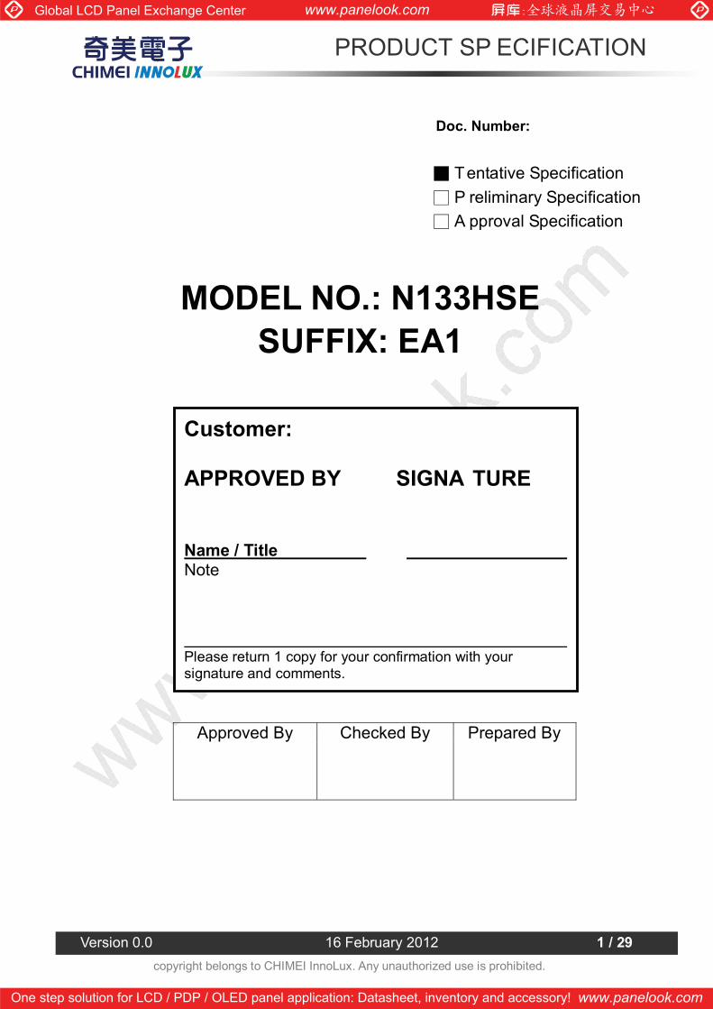
Customer: APPROVED BY SIGNA TURE Name / Title Note Please return 1 copy for your confirmation with your signature and comments.
Doc. Number:
Tentative Specification P reliminary Specification A pproval Specification
MODEL NO.: N133HSE SUFFIX: EA1
Approved By Checked By Prepared By
http://www.Datasheet4U.com

Global LCD Panel Exchange Center www.panelook.com
One step solution for LCD / PDP / OLED panel application: Datasheet, inventory and accessory! www.panelook.com
PRODUCT SP ECIFICATION
Version 0.0 16 February 2012 2 / 29
copyright belongs to CHIMEI InnoLux. Any unauthorized use is prohibited.
CONTENTS 1. GENERAL DESCRIPTION ......................................................................................................... 4
1.1 OVERVIEW ........................................................................................................................... 4 1.2 GENERAL SPECIFICATI0NS................................................................................................ 4
2. MECHANICAL SPECIFICATIONS ............................................................................................. 4 2.1 CONNECTOR TYPE.............................................................................................................. 4
3. ABSOLUTE MAXIMUM RATINGS ............................................................................................. 5 3.1 ABSOLUTE RATINGS OF ENVIRONMENT ....................................................................... 5 3.2 ELECTRICAL ABSOLUTE RATINGS .................................................................................. 5
3.2.1 TFT LCD MODULE ........................................................................................................5 4. ELECTRICAL SPECIFICATIONS............................................................................................... 6
4.1 FUNCTION BLOCK DIAGRAM........................................................................................... 6 4.2. INTERFACE CONNECTIONS.............................................................................................. 6 4.3 ELECTRICAL CHARACTERISTICS .................................................................................... 8
4.3.1 LCD ELETRONICS SPECIFICATION............................................................................8 4.3.2 LED CONVERTER SPECIFICATION........................................................................... 10 4.3.3 BACKLIGHT UNIT....................................................................................................... 12
4.4 DISPLAY PORT SIGNAL TIMING SPECIFICATION......................................................... 13 4.4.1 DISPLAY PORT INTERFACE....................................................................................... 13
4.5 DISPLAY TIMING SPECIFICATIONS................................................................................ 14 4.6 POWER ON/OFF SEQUENCE ............................................................................................ 15
5. OPTICAL CHARACTERISTICS ............................................................................................... 17 5.1 TEST CONDITIONS............................................................................................................ 17 5.2 OPTICAL SPECIFICATIONS .............................................................................................. 17
6. RELIABILITY TEST ITEM ....................................................................................................... .20 7. PACKING..................................................................................................................... ............. 21
7.1 MODULE LABEL................................................................................................................ 21 7.2 CARTON ..................................................................................................................... ......... 22 7.3 PALLET..................................................................................................................... ........... 23
8. PRECAUTIONS ................................................................................................................. ....... 24 8.1 HANDLING PRECAUTIONS.............................................................................................. 24 8.2 STORAGE PRECAUTIONS ................................................................................................ 24 8.3 OPERATION PRECAUTIONS............................................................................................. 24 Appendix. EDID DATA STRUCTURE....................................................................................... 25 Appendix. OUTLINE DRAWING .............................................................................................. 28

Global LCD Panel Exchange Center www.panelook.com
One step solution for LCD / PDP / OLED panel application: Datasheet, inventory and accessory! www.panelook.com
PRODUCT SP ECIFICATION
Version 0.0 16 February 2012 3 / 29
copyright belongs to CHIMEI InnoLux. Any unauthorized use is prohibited.
REVISION HISTORY
Version Date Page Description
0.0 Feb.16, 2012 All Spec. Ver. 0.0 was first issued.
Global LCD Panel Exchange Center www.panelook.com
One step solution for LCD / PDP / OLED panel application: Datasheet, inventory and accessory! www.panelook.com
PRODUCT SP ECIFICATION
Version 0.0 16 February 2012 4 / 29
copyright belongs to CHIMEI InnoLux. Any unauthorized use is prohibited.
1. GENERAL DESCRIPTION 1.1 OVERVIEW
N133HSE – EA1 is a 13.3” TFT Liquid Crystal Display module with LED Backlight unit and 30 pins eDP
interface. This module s upports 1920 x 1080 F HD mode and c an d isplay 16, 777,216 c olors. The
optimum viewing angle is at 6 o’clock direction. The converter module for Backlight is built in.
1.2 GENERAL SPECIFICATI0NS Item S pecification Unit Note Screen Size 13.3 diagonal Driver Element a-si TFT active matrix - - Pixel Number 1920 x R.G.B. x 1080 pixel - Pixel Pitch 0.1529 (H) x 0.1529 (V) mm - Pixel Arrangement RGB vertical stripe - - Display Colors 16,777,216 color - Transmissive Mode Normally black - - Surface Treatment Hard coating (3H), Anti-Glare - - Luminance, White 350 Cd/m2 Power Consumption Total (6.39 W)(Max.) @ cell (1.24W)(Max.), BL (5.15 W)(Max.) (1)
Note (1) The specified power consumption (with converter efficiency) is under t he conditions at VCCS =
3.3 V, fv = 60 Hz , LED_VCCS = Typ, fPWM = 200 Hz , Duty=100% and Ta = 25 ± 2 ºC, whereas mosaic
pattern is displayed.
2. MECHANICAL SPECIFICATIONS Item Mi n. Typ. Max. Unit Note
Horizontal (H) 305.05 305.35 305. 65 m m Vertical (V) (W/ PCBA) 187.47 187.77 188.07 mm Module Size Thickness (T) (W/ PCBA) NA 2.7 2.85 mm
(1)
Horizontal 293.46 293.76 294. 06 m m Active Area
Vertical 164.94 165.24 165. 54 m m Weight - 245 260 g
Note (1) Please refer to the attached drawings for more information of front and back outline dimensions.
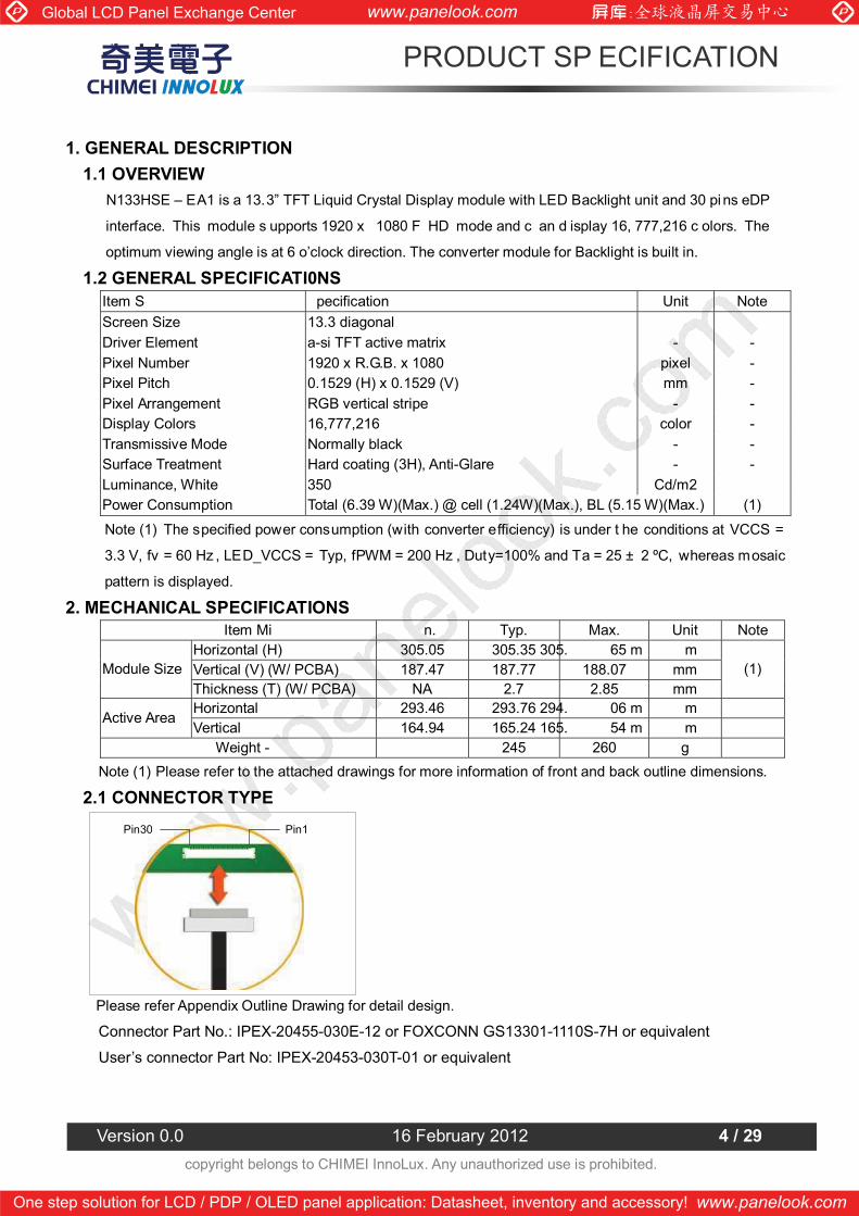
2.1 CONNECTOR TYPE
Please refer Appendix Outline Drawing for detail design.
Connector Part No.: IPEX-20455-030E-12 or FOXCONN GS13301-1110S-7H or equivalent User’s connector Part No: IPEX-20453-030T-01 or equivalent
Pin1 Pin30

Global LCD Panel Exchange Center www.panelook.com
One step solution for LCD / PDP / OLED panel application: Datasheet, inventory and accessory! www.panelook.com
PRODUCT SP ECIFICATION
Version 0.0 16 February 2012 5 / 29
copyright belongs to CHIMEI InnoLux. Any unauthorized use is prohibited.
3. ABSOLUTE MAXIMUM RATINGS 3.1 ABSOLUTE RATINGS OF ENVIRONMENT
Value Item Symbol
Min. Max. Unit Not e
Storage Temperature TST -20 +60 ºC (1) Operating Ambient Temperature TOP 0 +50 ºC (1), (2)
Note (1) (a) 90 %RH Max. (Ta <= 40 ºC).
(b) Wet-bulb temperature should be 39 ºC Max. (Ta > 40 ºC).
(c) No condensation.
Note (2) The temperature of panel surface should be 0 ºC min. and 60 ºC max.
3.2 ELECTRICAL ABSOLUTE RATINGS 3.2.1 TFT LCD MODULE
Value Item S ymbol Min. Ma x.
Unit Note
Power Supply Voltage VCCS -0.3 +4.0 V Logic Input Voltage VIN - 0.3 VCCS+0.3 V
(1)
Converter Input Voltage LED_VCCS -0.3 (25) V Converter Control Signal Voltage LED_PWM, -0.3 (5) V Converter Control Signal Voltage LED_EN -0.3 (5) V
Note ( 1) Stresses bey ond t hose listed in abo ve “ ELECTRICAL A BSOLUTE R ATINGS” may c ause
permanent da mage to the de vice. Nor mal oper ation s hould be r estricted t o t he c onditions
described in “ELECTRICAL CHARACTERISTICS”.
Storage Range
Relative Humidity (%RH)
Operating
Temperature (ºC)
100
80 60 -20 40 0 20 -40
80
40
60
20 10
90

Global LCD Panel Exchange Center www.panelook.com
One step solution for LCD / PDP / OLED panel application: Datasheet, inventory and accessory! www.panelook.com
PRODUCT SP ECIFICATION
Version 0.0 16 February 2012 6 / 29
copyright belongs to CHIMEI InnoLux. Any unauthorized use is prohibited.
4. ELECTRICAL SPECIFICATIONS 4.1 FUNCTION BLOCK DIAGRAM
4.2. INTERFACE CONNECTIONS
PIN ASSIGNMENT Pin Sy mbol Description Remark 1 NC No Connection (Reserved for CMI test) 2 H_GND High Speed Ground 3 ML1- Complement Signal-Lane 0 4 ML1+ True Signal-Main Lane 0 5 H_GND High Speed Ground 6 M L0- Complement Signal-Lane 0 7 ML0+ True Signal-Main Lane 0 8 H_GND High Speed Ground 9 AUX+ True Signal-Auxiliary Channel
10 A UX- Complement Signal-Auxiliary Channel 11 H_GND High Speed Ground 12 VCCS Power Supply +3.3 V (typical)
13 VCCS Power Supply +3.3 V (typical) 14 NC No Connection (Reserved for CMI test) 15 GND Ground
16 G ND Ground 17 HPD Hot Plug Detect
18 B L_GND BL Ground
19 B L_GND BL Ground 20 B L_GND BL Ground 21 B L_GND BL Ground 22 LED_EN BL_Enable Signal of LED Converter
EDID EEPROM
Display port Signals
VCCS
GND
TFT LCD PANEL
SCA
N D
RIVER
IC
BACKLIGHT UNIT
DP INPUT /
TIMING CONTROLLER
DATA DRIVER IC
DC/DC CONVERTER & REFERENCE VOLTAGE
GENERATOR
INPU
T CON
NEC
TOR
LED CONVERTER
Converter Input Signals
Global LCD Panel Exchange Center www.panelook.com
One step solution for LCD / PDP / OLED panel application: Datasheet, inventory and accessory! www.panelook.com
PRODUCT SP ECIFICATION
Version 0.0 16 February 2012 7 / 29
copyright belongs to CHIMEI InnoLux. Any unauthorized use is prohibited.
23 LE D_PWM PWM Dimming Control Signal of LED Converter
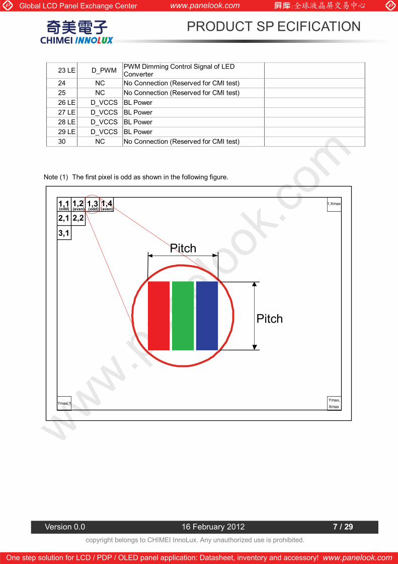
24 NC No Connection (Reserved for CMI test) 25 NC No Connection (Reserved for CMI test) 26 LE D_VCCS BL Power 27 LE D_VCCS BL Power 28 LE D_VCCS BL Power 29 LE D_VCCS BL Power 30 NC No Connection (Reserved for CMI test)
Note (1) The first pixel is odd as shown in the following figure.
1,1 (odd) 1,2
(even) 1,3 (odd) 1,4
(even) 2,1 2,2
3,1
Ymax,1 Ymax, Xmax
1,Xmax
Pitch
Pitch

Global LCD Panel Exchange Center www.panelook.com
One step solution for LCD / PDP / OLED panel application: Datasheet, inventory and accessory! www.panelook.com
PRODUCT SP ECIFICATION
Version 0.0 16 February 2012 8 / 29
copyright belongs to CHIMEI InnoLux. Any unauthorized use is prohibited.
4.3 ELECTRICAL CHARACTERISTICS 4.3.1 LCD ELETRONICS SPECIFICATION
Value Parameter Sy mbol
Min. T yp. Max. Unit Not e
Power Supply Voltage VCCS 3.0 3.3 3.6 V (1)-
High Level 2.25 - 2.75 V HPD
Low Level 0 - 0.4 V
Ripple Voltage VRP - 5 0 - mV (1)-
Inrush Current IRUSH - - 1.5 A (1),(2)
Mosaic (343) (376) mA (3)a Power Supply Current
White lcc
( 408) (448) mA (3)b
Note (1) The ambient temperature is Ta = 25 ± 2 ºC.
Note (2) IRUSH: the maximum current when VCCS is rising
IIS: the maximum current of the first 100ms after power-on
Measurement Conditions: Shown as the following figure. Test pattern: black.
R1
(High to Low) (Control Signal)
+12V
SW Q2
C1
1uF
VCCS +3.3V
2SK1470
Q1 2SK1475
47K
R2
1K
VR1 47K C2
0.01uF
C3 1uF
FUSE (LCD Module Input)
VCCS rising time is 0.5ms

Global LCD Panel Exchange Center www.panelook.com
One step solution for LCD / PDP / OLED panel application: Datasheet, inventory and accessory! www.panelook.com
PRODUCT SP ECIFICATION
Version 0.0 16 February 2012 9 / 29
copyright belongs to CHIMEI InnoLux. Any unauthorized use is prohibited.
Note (3) The specified power supply current is under the conditions at VCCS = 3.3 V, Ta = 25 ± 2 ºC, DC
Current and fv = 60 Hz, whereas a power dissipation check pattern below is displayed.
Active Area
a. Mosaic Pattern
Active Area
b. White Pattern
Global LCD Panel Exchange Center www.panelook.com
One step solution for LCD / PDP / OLED panel application: Datasheet, inventory and accessory! www.panelook.com
PRODUCT SP ECIFICATION
Version 0.0 16 February 2012 10 / 29
copyright belongs to CHIMEI InnoLux. Any unauthorized use is prohibited.
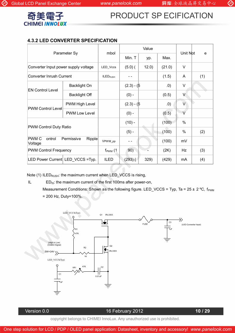
4.3.2 LED CONVERTER SPECIFICATION Value
Parameter Sy mbol Min. T yp. Max.
Unit Not e
Converter Input power supply voltage LED_Vccs (5.0) ( 12.0) (21.0) V
Converter Inrush Current ILEDRUSH - - (1.5) A (1)
Backlight On (2.3) - (5 .0) V EN Control Level
Backlight Off
(0) - (0.5) V
PWM High Level (2.3) - (5 .0) V PWM Control Level
PWM Low Level
(0) - (0.5) V
(10) - (100) % PWM Control Duty Ratio
(5) - (100) % (2)
PWM C ontrol Permissive Ripple Voltage VPWM_pp - - (100) mV
PWM Control Frequency fPWM (1 90) - (2K) Hz (3)
LED Power Current LED_VCCS =Typ. ILED (293) ( 329) (429) mA (4)
Note (1) ILEDRUSH: the maximum current when LED_VCCS is rising,
IL EDIS: the maximum current of the first 100ms after power-on,
Measurement Conditions: Shown as the following figure. LED_VCCS = Typ, Ta = 25 ± 2 ºC, fPWM
= 200 Hz, Duty=100%.
R1
(High to Low) (Control Signal)
LED_VCCS(Typ)
SW=24V
Q2
C1
1uF
LED_VCCS(Typ)
IRL3303
Q1 IRL3303
47K
R2
1K
VR1 47K C2
0.01uF
C3 1uF
FUSE (LED Converter Input)

Global LCD Panel Exchange Center www.panelook.com
One step solution for LCD / PDP / OLED panel application: Datasheet, inventory and accessory! www.panelook.com
PRODUCT SP ECIFICATION
Version 0.0 16 February 2012 11 / 29
copyright belongs to CHIMEI InnoLux. Any unauthorized use is prohibited.
90%
10%
0.5ms
0V
ILEDRushILEDIS
ILED
LED_VCC
100ms
LED_PWM
LED_EN
0V
0V
Note (2) If the PWM control duty ratio i s less than 10%, there is some possibility that acoustic noise or
backlight flash can be found. And it is also difficult to control the brightness linearity.
Note (3) If PWM control frequency is applied in the range less than 1KHz, the “waterfall” phenomenon on
the screen may be found. To avoid the issue, i t’s a s uggestion t hat PWM c ontrol frequency should
follow the criterion as below.
PWM control frequency fPWM should be in the range
≤∗+ fN )33.0( fPWM fN ∗+≤ )66.0(
N : Integer )3( ≥N
f : Frame rate
Note (4) The specified LED power supply current is under the conditions at “LED_VCCS = Typ.”, Ta = 25
± 2 ºC, fPWM = 200 Hz, Duty=100%.
VLED rising time is 0.5ms

Global LCD Panel Exchange Center www.panelook.com
One step solution for LCD / PDP / OLED panel application: Datasheet, inventory and accessory! www.panelook.com
PRODUCT SP ECIFICATION
Version 0.0 16 February 2012 12 / 29
copyright belongs to CHIMEI InnoLux. Any unauthorized use is prohibited.
4.3.3 BACKLIGHT UNIT Ta = 25 ± 2 ºC
Value Pa rameter Symbol Min. T yp. Max. Unit Not e
LED Light Bar Power Supply Voltage VL 25.2 27 29. 7 V
LED Light Bar Power Supply Current IL 125. 4 132 138.6 mA
(1)(2)(Duty100%)
Power Consumption PL 3. 160 3.564 4.116 W (3) LED Life Time LBL 12, 000 - - Hrs (4)
Note (1) LED current is measured by utilizing a high frequency current meter as shown below :
Note (2) For better LED light bar driving quality, it is recommended to utilize the adaptive boost converter with
current balancing function to drive LED light-bar.
Note (3) PL = IL ×VL (Without LED converter transfer efficiency)
Note (4) The lifetime of LED is defined as the time when it continues to operate under the conditions at Ta = 25 ±2 oC and IL = 20 mA(Per EA) until the brightness becomes 50% of its original value.
LED
Light Bar
VL, IL
Light Bar Feedback
Channels

Global LCD Panel Exchange Center www.panelook.com
One step solution for LCD / PDP / OLED panel application: Datasheet, inventory and accessory! www.panelook.com
PRODUCT SP ECIFICATION
Version 0.0 16 February 2012 13 / 29
The copyright belongs to CHIMEI InnoLux. Any unauthorized use is prohibited.
4.4 DISPLAY PORT SIGNAL TIMING SPECIFICATION 4.4.1 DISPLAY PORT INTERFACE
Parameter Sy mbol Min. Typ. Max. Unit Notes
Differential Signal Common Mode Voltage(MainLink and AUX) VCM 0 2 V (1)(3)
AUX AC Coupling Capacitor CAUX 75 200 nF (2) Note (1) Display port i nterface rel ated AC coupled s ignals s hould follow VESA Di splayPort S tandard
Version1. Revision 1a and VESA Embedded DisplayPortTM Standard Version 1.1.
(2) The AUX AC Coupling Capacitor should be placed on Source Devices.
(3)The s ource de vice s hould p ass t he t est c riteria des cribed i n D isplayPortCompliance Test
Specification (CTS) 1.1
0V
VCM |VID|
Single Ended
VD+
VD-
Global LCD Panel Exchange Center www.panelook.com
One step solution for LCD / PDP / OLED panel application: Datasheet, inventory and accessory! www.panelook.com
PRODUCT SP ECIFICATION
Version 0.0 16 February 2012 14 / 29
The copyright belongs to CHIMEI InnoLux. Any unauthorized use is prohibited.
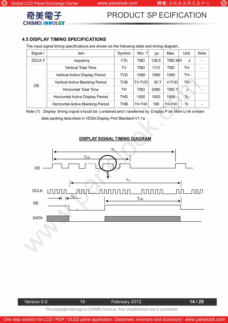
4.5 DISPLAY TIMING SPECIFICATIONS The input signal timing specifications are shown as the following table and timing diagram.
Signal I tem Symbol Min. T yp. Max. Unit Note
DCLK F requency 1/Tc TBD 138.5 TBD MH z -
Vertical Total Time TV TBD 1112 TBD TH -
Vertical Active Display Period TVD 1080 1080 1080 TH -
Vertical Active Blanking Period TVB TV-TVD 30 T V-TVD TH -
Horizontal Total Time TH TBD 2080 TBD T c -
Horizontal Active Display Period THD 1920 1920 1920 Tc -
DE
Horizontal Active Blanking Period THB TH-THD 160 TH-THD Tc -
Note (1) Display timing s ignal should be c ontained and t ransferred by D isplay P ort Main Li nk s tream
data packing described in VESA Display Port Standard V1.1a
DISPLAY SIGNAL TIMING DIAGRAM
TH
TC DCLK
THD
TVD
Tv
DE
DE
DATA
Global LCD Panel Exchange Center www.panelook.com
One step solution for LCD / PDP / OLED panel application: Datasheet, inventory and accessory! www.panelook.com
PRODUCT SP ECIFICATION
Version 0.0 16 February 2012 15 / 29
The copyright belongs to CHIMEI InnoLux. Any unauthorized use is prohibited.
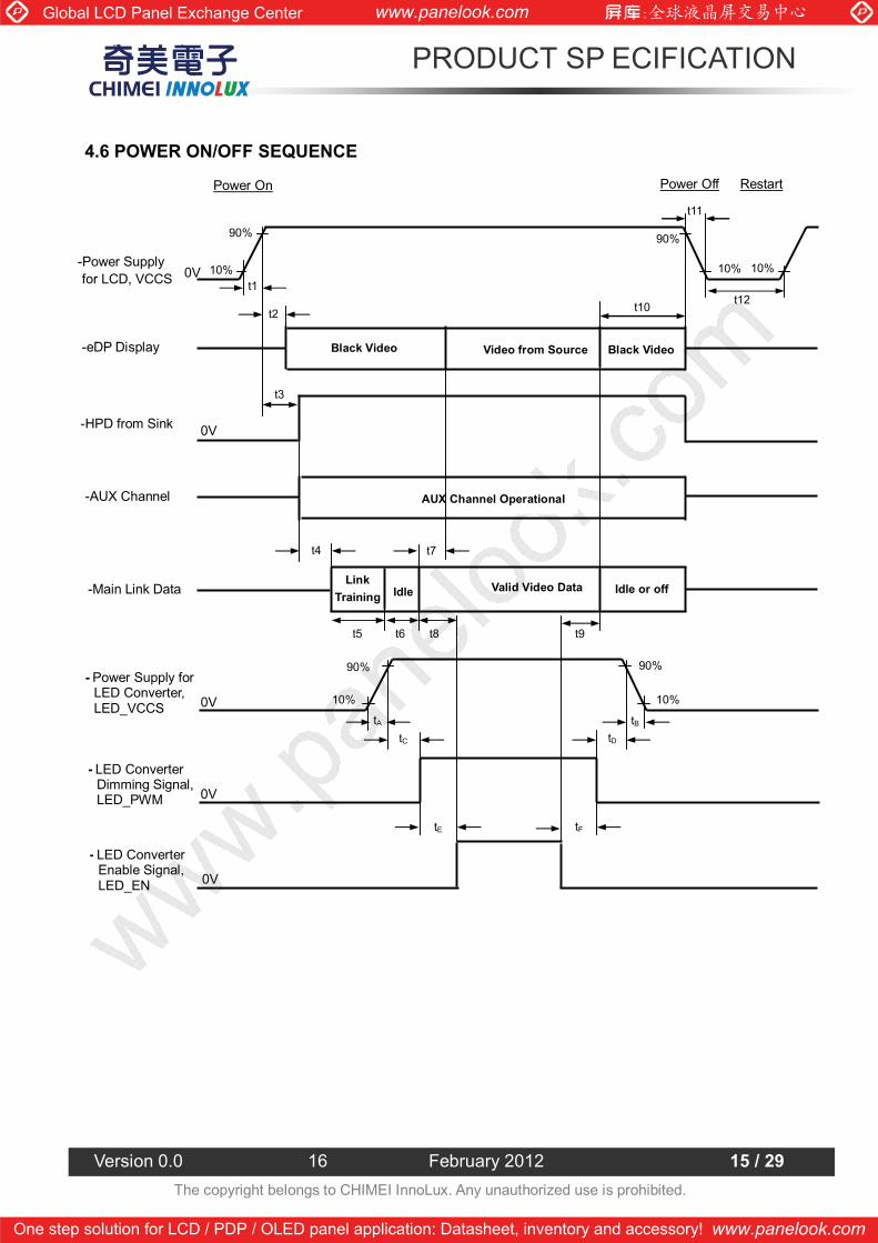
4.6 POWER ON/OFF SEQUENCE
t1 t12
Restart Power On Power Off
10% t10 t2
90% 10%
90%
Black Video
t11
10%
Black Video Video from Source
t3
AUX Channel Operational
Link Training Idle Valid Video Data
tA 0V
0V
0V
tC
tE
tB
Idle or off
t4
t5 t6
t7
t8 t9
-Power Supply for LCD, VCCS 0V
0V
90% 10%
tF
tD
-eDP Display
-HPD from Sink
-AUX Channel
-Main Link Data
- Power Supply for LED Converter, LED_VCCS
- LED Converter Dimming Signal, LED_PWM
- LED Converter Enable Signal, LED_EN
90% 10%
Global LCD Panel Exchange Center www.panelook.com
One step solution for LCD / PDP / OLED panel application: Datasheet, inventory and accessory! www.panelook.com
PRODUCT SP ECIFICATION
Version 0.0 16 February 2012 16 / 29
The copyright belongs to CHIMEI InnoLux. Any unauthorized use is prohibited.
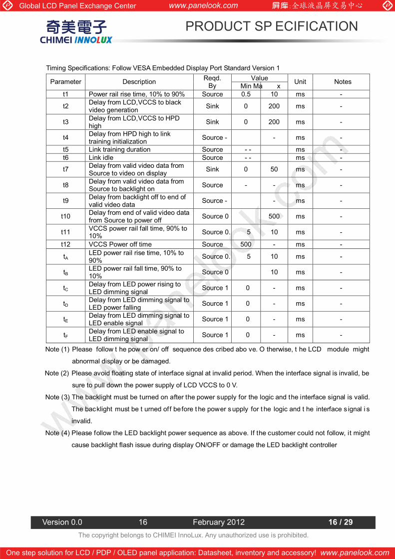
Timing Specifications: Follow VESA Embedded Display Port Standard Version 1 Value Parameter Description Reqd.
By Min Ma x Unit Notes
t1 Power rail rise time, 10% to 90% Source 0.5 10 ms -
t2 Delay from LCD,VCCS to black video generation Sink 0 200 ms -
t3 Delay from LCD,VCCS to HPD high Sink 0 200 ms -
t4 Delay from HPD high to link training initialization Source - - ms -
t5 Link training duration Source - - ms - t6 Link idle Source - - ms -
t7 Delay from valid video data from Source to video on display Sink 0 50 ms -
t8 Delay from valid video data from Source to backlight on Source - - ms -
t9 Delay from backlight off to end of valid video data Source - - ms -
t10 Delay from end of valid video data from Source to power off Source 0 500 ms -
t11 VCCS power rail fall time, 90% to 10% Source 0. 5 10 ms -
t12 VCCS Power off time Source 500 - ms -
tA LED power rail rise time, 10% to 90% Source 0. 5 10 ms -
tB LED power rail fall time, 90% to 10% Source 0 10 ms -
tC Delay from LED power rising to LED dimming signal Source 1 0 - ms -
tD Delay from LED dimming signal to LED power falling Source 1 0 - ms -
tE Delay from LED dimming signal to LED enable signal Source 1 0 - ms -
tF Delay from LED enable signal to LED dimming signal Source 1 0 - ms -
Note (1) Please follow t he pow er on/ off sequence des cribed abo ve. O therwise, t he LCD module might
abnormal display or be damaged.
Note (2) Please avoid floating state of interface signal at invalid period. When the interface signal is invalid, be
sure to pull down the power supply of LCD VCCS to 0 V.
Note (3) The backlight must be turned on after the power supply for the logic and the interface signal is valid.
The backlight must be t urned of f before t he power s upply for t he logic and t he interface s ignal i s
invalid.
Note (4) Please follow the LED backlight power sequence as above. If the customer could not follow, it might
cause backlight flash issue during display ON/OFF or damage the LED backlight controller
Global LCD Panel Exchange Center www.panelook.com
One step solution for LCD / PDP / OLED panel application: Datasheet, inventory and accessory! www.panelook.com
PRODUCT SP ECIFICATION
Version 0.0 16 February 2012 17 / 29
The copyright belongs to CHIMEI InnoLux. Any unauthorized use is prohibited.
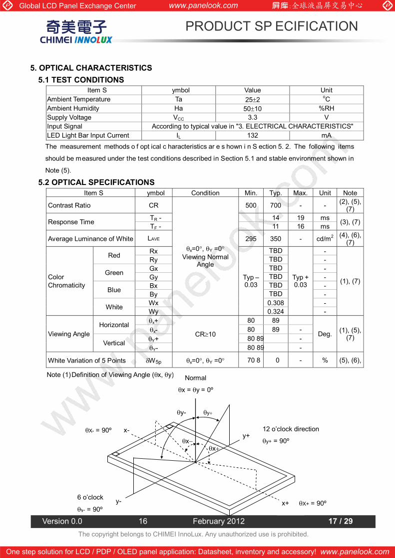
5. OPTICAL CHARACTERISTICS 5.1 TEST CONDITIONS
Item S ymbol Value Unit Ambient Temperature Ta 25±2 oC Ambient Humidity Ha 50±10 %RH Supply Voltage VCC 3.3 V Input Signal According to typical value in "3. ELECTRICAL CHARACTERISTICS" LED Light Bar Input Current IL 132 mA
The measurement methods o f opt ical c haracteristics ar e s hown i n S ection 5. 2. The following items
should be measured under the test conditions described in Section 5.1 and stable environment shown in
Note (5).
5.2 OPTICAL SPECIFICATIONS Item S ymbol Condition Min. Typ. Max. Unit Note
Contrast Ratio CR 500 700 - - (2), (5), (7)
TR - 14 19 ms Response Time TF - 11 16 ms
(3), (7)
Average Luminance of White LAVE 295 350 - cd/m2 (4), (6), (7)
Rx TBD - Red Ry TBD - Gx TBD - Green Gy TBD - Bx TBD - Blue By TBD - Wx 0.308 -
Color Chromaticity
White Wy
θx=0°, θY =0° Viewing Normal
Angle
Typ – 0.03
0.324
Typ + 0.03
-
(1), (7)
θx+ 80 89 Horizontal
θx- 80 89 - θY+ 80 89 -
Viewing Angle Vertical
θY-
CR≥10
80 89 -
Deg. (1), (5), (7)
White Variation of 5 Points δW5p θx=0°, θY =0° 70 8 0 - % (5), (6),
Note (1) Definition of Viewing Angle (θx, θy):
12 o’clock direction
θy+ = 90º
6 o’clock
θy- = 90º
θx− θx+
θy- θy+
x- y+
y- x+
Normal
θx = θy = 0º
θX+ = 90º
θX- = 90º
Global LCD Panel Exchange Center www.panelook.com
One step solution for LCD / PDP / OLED panel application: Datasheet, inventory and accessory! www.panelook.com
PRODUCT SP ECIFICATION
Version 0.0 16 February 2012 18 / 29
The copyright belongs to CHIMEI InnoLux. Any unauthorized use is prohibited.
Note (2) Definition of Contrast Ratio (CR):
The contrast ratio can be calculated by the following expression.
Contrast Ratio (CR) = L63 / L0
L63: Luminance of gray level 63
L 0: Luminance of gray level 0
CR = CR (1)
CR (X) is corresponding to the Contrast Ratio of the point X at Figure in Note (6).
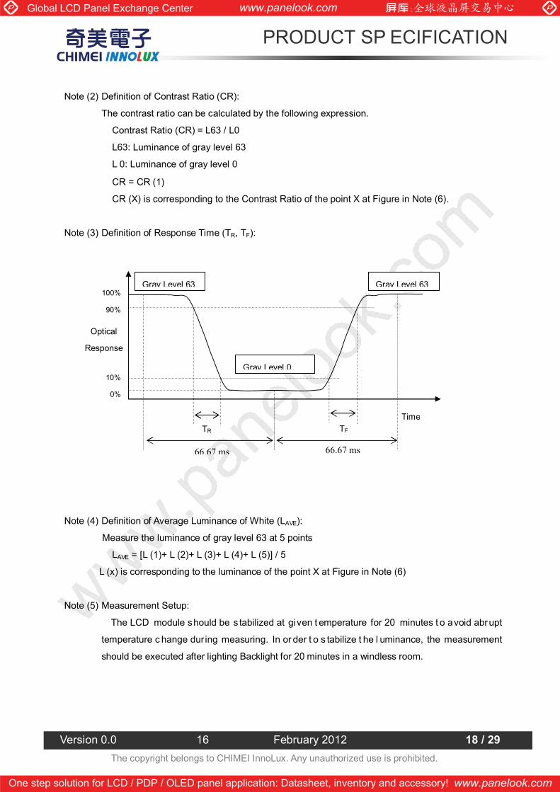
Note (3) Definition of Response Time (TR, TF):
Note (4) Definition of Average Luminance of White (LAVE):
Measure the luminance of gray level 63 at 5 points
LAVE = [L (1)+ L (2)+ L (3)+ L (4)+ L (5)] / 5
L (x) is corresponding to the luminance of the point X at Figure in Note (6)
Note (5) Measurement Setup:
The LCD module should be s tabilized at given t emperature for 20 minutes t o avoid abrupt
temperature c hange during measuring. In or der t o s tabilize t he l uminance, the measurement
should be executed after lighting Backlight for 20 minutes in a windless room.
100%
90%
10%
0%
Gray Level 63
Gray Level 0
Gray Level 63
Time TF
Optical
Response
TR
66.67 ms 66.67 ms

Global LCD Panel Exchange Center www.panelook.com
One step solution for LCD / PDP / OLED panel application: Datasheet, inventory and accessory! www.panelook.com
PRODUCT SP ECIFICATION
Version 0.0 16 February 2012 19 / 29
The copyright belongs to CHIMEI InnoLux. Any unauthorized use is prohibited.
CS - 2000T
500 mm
LCD M odule
LCD P anel
Center of the S creen Light Shield Room ( Ambient L uminance < 2 l u x)
USB2000
Note (6) Definition of White Variation (δW):
Measure the luminance of gray level 63 at 5 points
δW5p = {Minimum [L (1)~L (5)] / Maximum [L (1)~ L (5)]}*100%
Active area
Note (7) The listed optical specifications refer to the initial value of manufacture, but the condition of
the specifications after long-term operation will not be warranted.
: Test Point
X=1 to 13
X
or equivalent or equivalent
Global LCD Panel Exchange Center www.panelook.com
One step solution for LCD / PDP / OLED panel application: Datasheet, inventory and accessory! www.panelook.com
PRODUCT SP ECIFICATION
Version 0.0 16 February 2012 20 / 29
The copyright belongs to CHIMEI InnoLux. Any unauthorized use is prohibited.
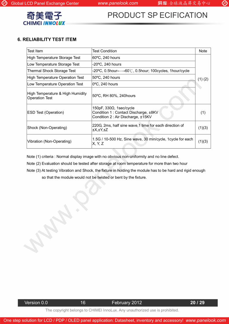
6. RELIABILITY TEST ITEM
Test Item Test Condition Note
High Temperature Storage Test 60ºC, 240 hours
Low Temperature Storage Test -20ºC, 240 hours
Thermal Shock Storage Test -20ºC, 0.5hour←→60 , 0.5hour; 100cycles, 1hour/cycle
High Temperature Operation Test 50ºC, 240 hours
Low Temperature Operation Test 0ºC, 240 hours
High Temperature & High Humidity Operation Test 50ºC, RH 80%, 240hours
(1) (2)
ESD Test (Operation) 150pF, 330Ω, 1sec/cycle Condition 1 : Contact Discharge, ±8KV Condition 2 : Air Discharge, ±15KV
(1)
Shock (Non-Operating) 220G, 2ms, half sine wave,1 time for each direction of ±X,±Y,±Z (1)(3)
Vibration (Non-Operating) 1.5G / 10-500 Hz, Sine wave, 30 min/cycle, 1cycle for each X, Y, Z (1)(3)
Note (1) criteria : Normal display image with no obvious non-uniformity and no line defect.
Note (2) Evaluation should be tested after storage at room temperature for more than two hour
Note (3) At testing Vibration and Shock, the fixture in holding the module has to be hard and rigid enough
so that the module would not be twisted or bent by the fixture.
Global LCD Panel Exchange Center www.panelook.com
One step solution for LCD / PDP / OLED panel application: Datasheet, inventory and accessory! www.panelook.com
PRODUCT SP ECIFICATION
Version 0.0 16 February 2012 21 / 29
The copyright belongs to CHIMEI InnoLux. Any unauthorized use is prohibited.
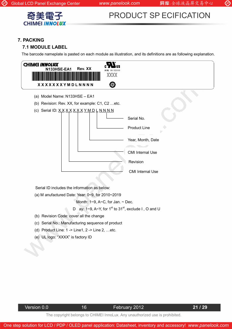
7. PACKING 7.1 MODULE LABEL The barcode nameplate is pasted on each module as illustration, and its definitions are as following explanation.
(a) Model Name: N133HSE – EA1
(b) Revision: Rev. XX, for example: C1, C2 …etc.
(c) Serial ID: X X X X X X X Y M D L N N N N
Serial ID includes the information as below:
(a) M anufactured Date: Year: 0~9, for 2010~2019
Month: 1~9, A~C, for Jan. ~ Dec.
D ay: 1~9, A~Y, for 1st to 31st, exclude I , O and U
(b) Revision Code: cover all the change
(c) Serial No.: Manufacturing sequence of product
(d) Product Line: 1 -> Line1, 2 -> Line 2, …etc.
(e) UL logo: “XXXX” is factory ID
N133HSE-EA1
X X X X X X X Y M D L N N N N
Product Line
Year, Month, Date
CMI Internal Use
Revision
CMI Internal Use
Serial No.
Rev. XX
Global LCD Panel Exchange Center www.panelook.com
One step solution for LCD / PDP / OLED panel application: Datasheet, inventory and accessory! www.panelook.com
PRODUCT SP ECIFICATION
Version 0.0 16 February 2012 22 / 29
The copyright belongs to CHIMEI InnoLux. Any unauthorized use is prohibited.
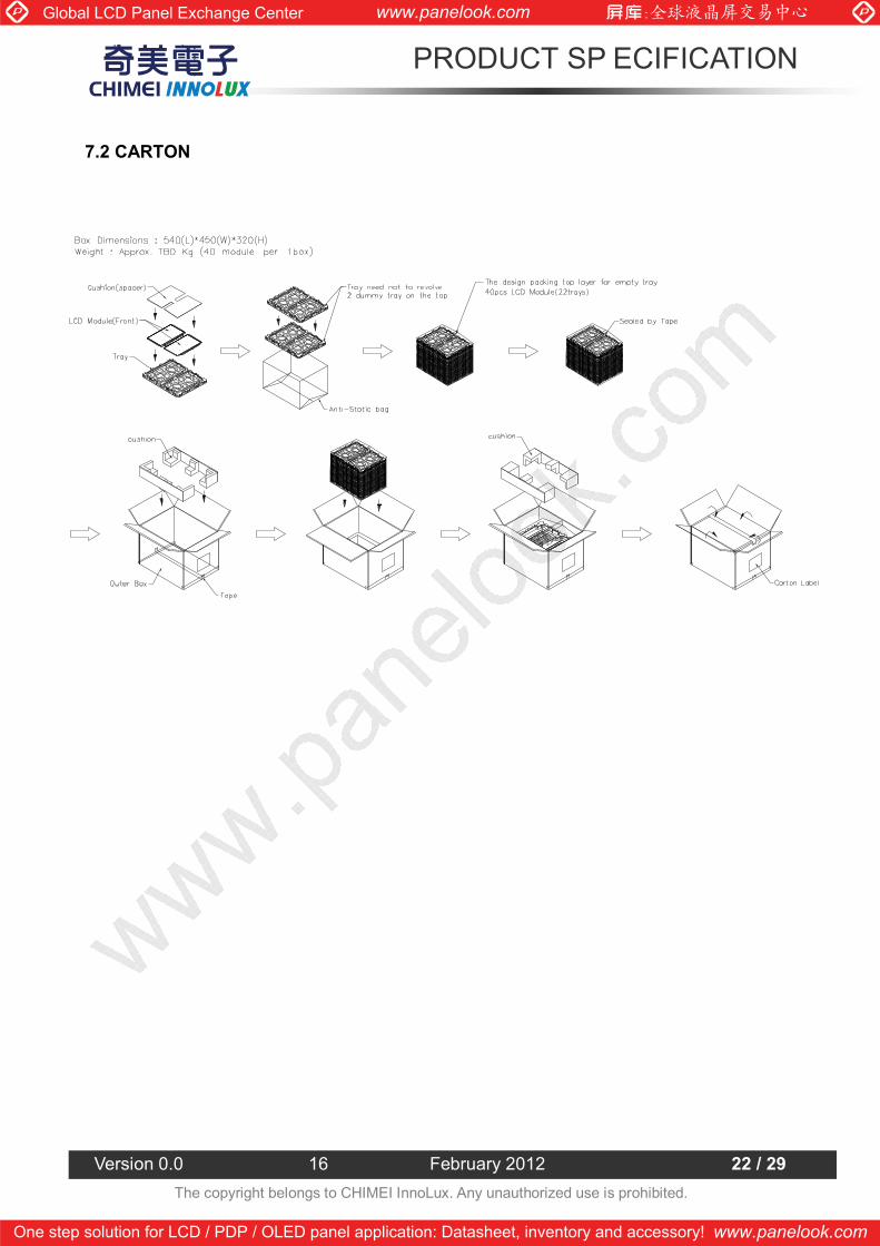
7.2 CARTON

Global LCD Panel Exchange Center www.panelook.com
One step solution for LCD / PDP / OLED panel application: Datasheet, inventory and accessory! www.panelook.com
PRODUCT SP ECIFICATION
Version 0.0 16 February 2012 23 / 29
The copyright belongs to CHIMEI InnoLux. Any unauthorized use is prohibited.
7.3 PALLET
Global LCD Panel Exchange Center www.panelook.com
One step solution for LCD / PDP / OLED panel application: Datasheet, inventory and accessory! www.panelook.com
PRODUCT SP ECIFICATION
Version 0.0 16 February 2012 24 / 29
The copyright belongs to CHIMEI InnoLux. Any unauthorized use is prohibited.
8. PRECAUTIONS 8.1 HANDLING PRECAUTIONS
(1) The module should be as sembled into the system firmly by using every mounting hole. Be careful
not to twist or bend the module.
(2) While assembling or installing modules, it can only be in the clean area. The dust and oil may cause
electrical short or damage the polarizer.
(3) Use f ingerstalls or s oft g loves i n or der t o k eep d isplay c lean dur ing the incoming inspection and
assembly process.
(4) Do not press or scratch the surface harder than a HB pencil lead on the panel because the polarizer
is very soft and easily scratched.
(5) If the surface of the polarizer is dirty, please clean it by some absorbent cotton or soft cloth. Do not
use K etone t ype materials ( ex. A cetone), E thyl al cohol, Toluene, E thyl ac id or M ethyl c hloride. It
might permanently damage the polarizer due to chemical reaction.
(6) Wipe off water droplets or oil immediately. Staining and discoloration may occur if they left on panel
for a long time.
(7) If the liquid crystal material leaks from the panel, it should be kept away from the eyes or mouth. In
case of contacting with hands, legs or clothes, it must be washed away thoroughly with soap.
(8) Protect the module from static electricity, it may cause damage to the C-MOS Gate Array IC.
(9) Do not disassemble the module.
(10) Do not pull or fold the LED wire.
(11) Pins of I/F connector should not be touched directly with bare hands.
8.2 STORAGE PRECAUTIONS
(1) High t emperature or humidity may r educe t he performance of module. P lease s tore LCD m odule
within the specified storage conditions.
(2) It is dangerous that moisture come i nto or contacted the LCD module, because the moisture may
damage LCD module when it is operating.
(3) It may reduce the display quality if the ambient temperature is lower than 10 ºC. For example, the
response t ime w ill bec ome s lowly, and t he s tarting voltage o f LE D w ill be hi gher than t he r oom
temperature.
8.3 OPERATION PRECAUTIONS (1) Do not pull the I/F connector in or out while the module is operating.
(2) Always f ollow t he correct power on/ off sequence whe n LCD module i s c onnecting and oper ating.
This can prevent the CMOS LSI chips from damage during latch-up.
(3) The s tartup voltage o f Backlight i s appr oximately 1000 Volts. I t may c ause el ectrical s hock w hile
assembling with converter. Do not disassemble the module or insert anything into the Backlight unit.

Global LCD Panel Exchange Center www.panelook.com
One step solution for LCD / PDP / OLED panel application: Datasheet, inventory and accessory! www.panelook.com
PRODUCT SP ECIFICATION
Version 0.0 16 February 2012 25 / 29
The copyright belongs to CHIMEI InnoLux. Any unauthorized use is prohibited.
Appendix. EDID DATA STRUCTURE The EDID (Extended Display Identification Data) data formats are to support displays as defined in the
VESA Plug & Display and FPDI standards. Byte
#(decimal) Byte
#(hex) Field Name and Comments Value (hex)
Value (binary)
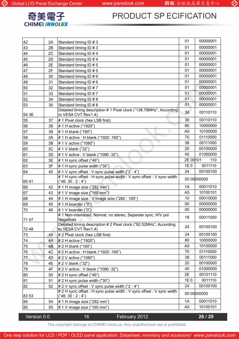
0 0 Header 00 00000000 1 1 Header FF 11111111 2 2 Header FF 11111111 3 3 Header FF 11111111 4 4 Header FF 11111111 5 5 Header FF 11111111 6 6 Header FF 11111111 7 7 Header 00 00000000 8 8 EISA ID manufacturer name (“CMN”) 0D 00001101 9 9 EISA ID manufacturer name (Compressed ASCII) AE 10101110 10 0A ID product code (N133HSE-EA1) 43 01000011 11 0B ID product code (hex LSB first; N133HSE-EA1) 13 00010011 12 0C ID S/N (fixed “0”) 00 00000000 13 0D ID S/N (fixed “0”) 00 00000000 14 0E ID S/N (fixed “0”) 00 00000000 15 0F ID S/N (fixed “0”) 00 00000000 16 10 Week of manufacture (fixed week code) 34 00110100 17 11 Year of manufacture (fixed year code) 15 00010101 18 12 EDID structure version # (“1”) 01 00000001 19 13 EDID revision # (“4”) 04 00000100 20 14 Vedio Input Definition A5 10100101 21 15 Max H image size (“28.186cm”) 1C 0001 1100 22 16 Max V image size (“16.524cm”) 10 00010000 23 17 Display Gamma (Gamma = ”2.2”) 78 01111000 24 18 Feature support 02 00000010 25 19 Red/Green (Rx1, Rx0, Ry1, Ry0, Gx1, Gx0, Gy1, Gy0) 93 10010011 26 1A Blue/White (Bx1, Bx0, By1, By0, Wx1, Wx0, Wy1, Wy0) AD 10101101 27 1B Red-x (Rx = “0.662”) A9 10101001 28 1C Red-y (Ry = “0.325”) 53 01010011 29 1D Green-x (Gx = ”0.296”) 4C 01001100 30 1E Green-y (Gy = ”0.588”) 96 10010110 31 1F Blue-x (Bx = ”0.146") 25 00100101 32 20 Blue-y (By = ”0.068”) 11 00010001 33 21 White-x (Wx = ”0.311”) 4F 01001111 34 22 White-y (Wy = ”0.325”) 53 01010011 35 23 Established timings 1 00 00000000 36 24 Established timings 2 00 00000000 37 25 Manufacturer’s reserved timings 00 00000000
38 26 Standard timing ID # 1 01 00000001 39 27 Standard timing ID # 1 01 00000001 40 28 Standard timing ID # 2 01 00000001 41 29 Standard timing ID # 2 01 00000001
Global LCD Panel Exchange Center www.panelook.com
One step solution for LCD / PDP / OLED panel application: Datasheet, inventory and accessory! www.panelook.com
PRODUCT SP ECIFICATION
Version 0.0 16 February 2012 26 / 29
The copyright belongs to CHIMEI InnoLux. Any unauthorized use is prohibited.
42 2A Standard timing ID # 3 01 00000001
43 2B Standard timing ID # 3 01 00000001 44 2C Standard timing ID # 4 01 00000001 45 2D Standard timing ID # 4 01 00000001 46 2E Standard timing ID # 5 01 00000001 47 2F Standard timing ID # 5 01 00000001 48 30 Standard timing ID # 6 01 00000001 49 31 Standard timing ID # 6 01 00000001 50 32 Standard timing ID # 7 01 00000001 51 33 Standard timing ID # 7 01 00000001 52 34 Standard timing ID # 8 01 00000001 53 35 Standard timing ID # 8 01 00000001
54 36 Detailed timing description # 1 Pixel clock (“138.78MHz”, According to VESA CVT Rev1.4) 36 00110110
55 37 # 1 Pixel clock (hex LSB first) 36 00110110 56 38 # 1 H active (“1920”) 80 10000000 57 39 # 1 H blank (“160”) A0 10100000 58 3A # 1 H active : H blank (“1920 :160”) 70 01110000 59 3B # 1 V active (”1080”) 38 00111000 60 3C # 1 V blank (”32”) 20 00100000 61 3D # 1 V active : V blank (”1080 :32”) 40 01000000 62 3E # 1 H sync offset (”46”) 2E 00101 110 63 3F # 1 H sync pulse width ("30”) 1E 0 0011110 64 40 # 1 V sync offset : V sync pulse width (”2 : 4”) 24 00100100
65 41 # 1 H sync offset : H sync pulse width : V sync offset : V sync width (”46: 30 : 2 : 4”) 00 00000000
66 42 # 1 H image size (”282 mm”) 1A 00011010 67 43 # 1 V image size (”165 mm”) A5 10100101 68 44 # 1 H image size : V image size (”282 : 165”) 10 00010000 69 45 # 1 H boarder (”0”) 00 00000000 70 46 # 1 V boarder (”0”) 00 00000000
71 47 # 1 Non-interlaced, Normal, no stereo, Separate sync, H/V pol Negatives 18 00011000
72 48 Detailed timing description # 2 Pixel clock (“92.52MHz”, According to VESA CVT Rev1.4) 24 00100100
73 49 # 2 Pixel clock (hex LSB first) 24 00100100 74 4A # 2 H active (“1920”) 80 10000000 75 4B # 2 H blank (“160”) A0 10100000 76 4C # 2 H active : H blank (“1920 :160”) 70 01110000 77 4D # 2 V active (”1080”) 38 00111000 78 4E # 2 V blank (”32”) 20 00100000 79 4F # 2 V active : V blank (”1080 :32”) 40 01000000 80 50 # 2 H sync offset (”46”) 2E 00101110 81 51 # 2 H sync pulse width ("30”) 1E 0 0011110 82 52 # 2 V sync offset : V sync pulse width (”2 : 4”) 24 00100100
83 53 # 2 H sync offset : H sync pulse width : V sync offset : V sync width (”46: 30 : 2 : 4”) 00 00000000
84 54 # 1 H image size (”282 mm”) 1A 00011010 85 55 # 1 V image size (”165 mm”) A5 10100101

Global LCD Panel Exchange Center www.panelook.com
One step solution for LCD / PDP / OLED panel application: Datasheet, inventory and accessory! www.panelook.com
PRODUCT SP ECIFICATION
Version 0.0 16 February 2012 27 / 29
The copyright belongs to CHIMEI InnoLux. Any unauthorized use is prohibited.
86 56 # 1 H image size : V image size (”282 : 165”) 10 00010000
87 57 # 2 H boarder (”0”) 00 00000000
88 58 # 2 V boarder (”0”) 00 00000000
89 59 # 2 Non-interlaced, Normal, no stereo, Separate sync, H/V pol Negatives 18 00011000
90 5A Detailed timing description # 3 00 00000000 91 5B # 3 Flag 00 00000000 92 5C # 3 Reserved 00 00000000 93 5D # 3 FE (hex) defines ASCII string (Vendor “CMO”, ASCII) FE 1111111 0 94 5E # 3 Flag 00 00000000 95 5F # 3 1st character of string (“C”) 43 01000011 96 60 # 3 2nd character of string (“M”) 4D 01001101 97 61 # 3 3rd character of string (“N”) 4E 01001 110 98 62 # 3 New line character indicates end of ASCII string 0A 00001010 99 63 # 3 Padding with “Blank” character 20 00100000 100 64 # 3 Padding with “Blank” character 20 00100000 101 65 # 3 Padding with “Blank” character 20 00100000 102 66 # 3 Padding with “Blank” character 20 00100000 103 67 # 3 Padding with “Blank” character 20 00100000 104 68 # 3 Padding with “Blank” character 20 00100000 105 69 # 3 Padding with “Blank” character 20 00100000 106 6A # 3 Padding with “Blank” character 20 00100000 107 6B # 3 Padding with “Blank” character 20 00100000 108 6C Detailed timing description # 4 00 00000000 109 6D # 4 Flag 00 00000000 110 6E # 4 Reserved 00 00000000
111 6 F # 4 FE (hex) defines ASCII string (Model Name“N156B3-L03”, ASCII) FE 1111111 0
112 70 # 4 Flag 00 00000000 113 71 # 4 1st character of name (“N”) 4E 01001110 114 72 # 4 2nd character of name (“1”) 31 00110001 115 73 # 4 3rd character of name (“3”) 33 00110011 116 74 # 4 4th character of name (“3”) 33 00110011 117 75 # 4 5th character of name (“H”) 48 01001000 118 76 # 4 6th character of name (“S”) 53 01010011 119 77 # 4 7th character of name (“E”) 45 01000101 120 78 # 4 8th character of name (“-”) 2D 00101101 121 79 # 4 9th character of name (“E”) 45 01000101 122 7A # 4 Ath character of name (“A”) 41 01000001 123 7B # 4 Bth character of name (“1”) 31 00110001 124 7C # 4 New line character indicates end of ASCII string 0A 00001010 125 7D # 4 Padding with “Blank” character 20 00100000 126 7E No extension 00 00000000 127 7F Checksum CD 11001101
Global LCD Panel Exchange Center www.panelook.com
One step solution for LCD / PDP / OLED panel application: Datasheet, inventory and accessory! www.panelook.com
PRODUCT SP ECIFICATION
Version 0.0 16 February 2012 28 / 29
The copyright belongs to CHIMEI InnoLux. Any unauthorized use is prohibited.
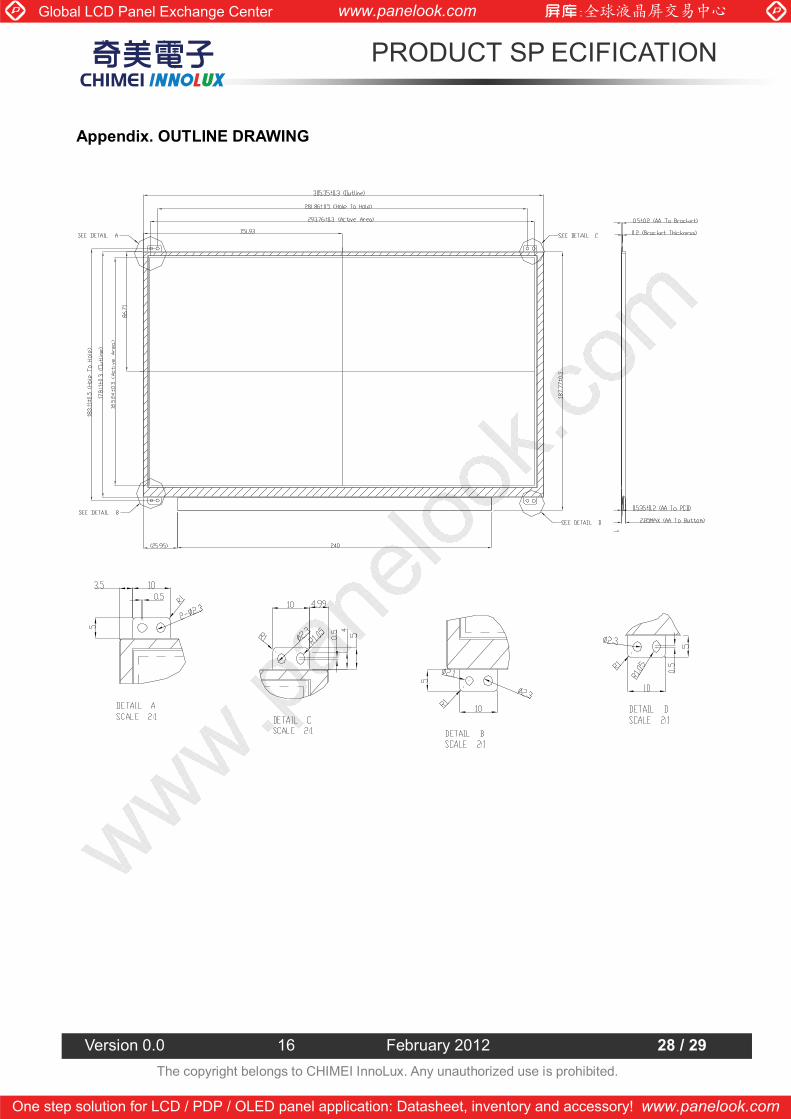
Appendix. OUTLINE DRAWING

Global LCD Panel Exchange Center www.panelook.com
One step solution for LCD / PDP / OLED panel application: Datasheet, inventory and accessory! www.panelook.com
PRODUCT SP ECIFICATION
Version 0.0 16 February 2012 29 / 29
The copyright belongs to CHIMEI InnoLux. Any unauthorized use is prohibited.