model predictive control circuit of the current source matrix … · in this paper, a new...
TRANSCRIPT

Journal of Power and Energy Engineering, 2015, 3, 136-145 Published Online April 2015 in SciRes. http://www.scirp.org/journal/jpee http://dx.doi.org/10.4236/jpee.2015.34020
How to cite this paper: Tadra, G., Fedyczak, Z. and Szcześniak, P. (2015) Model Predictive Control Circuit of the Current Source Matrix Converter. Journal of Power and Energy Engineering, 3, 136-145. http://dx.doi.org/10.4236/jpee.2015.34020
Model Predictive Control Circuit of the Current Source Matrix Converter Grzegorz Tadra, Zbigniew Fedyczak, Paweł Szcześniak Power Electronics Department, Institute of Electrical Engineering, University of Zielona Gora, Zielona Góra, Poland Email: [email protected], [email protected], [email protected] Received January 2015
Abstract In this paper, a new predictive control strategy for current source matrix converter (CSMC) is presented. Proposed predictive control strategy allows for creating output voltages with boost type voltage transfer ratio and desired frequency. The description of predictive control circuit of the CSMC is presented. Furthermore the simulation test results to confirm functionality of the proposed control strategy and converter properties under this strategy are shown.
Keywords AC/AC Frequency Converters, Current Source Matrix Converter, Predictive Control Strategy
1. Introduction An alternative for commonly used indirect (AC/DC/AC) frequency converters with DC storage elements is con-stantly searched for. One of the proposed alternatives is the direct voltage source matrix converter (VSMC). The main disadvantage of the VSMC, virtually limiting its industrial application in power networks or electric drives, is the relationship between the input and output voltages (voltage transfer ratio). The quotient of the rms values of these voltages (while retaining their sinusoidal shape) is lower than 1 [1]-[5]. In this respect, hybrid matrix converters, where an additional DC/DC converter and a small capacitor for energy storage are used, have more favorable properties due to the fact that their voltage transfer ratio can be higher than 1 [6] [7]. Such transfer ra-tio is also characteristic for direct and indirect matrix reactance frequency converters (MRFC) [8]-[11] and di-rect current source matrix converters (CSMC) [12]-[15]. MRFC and CSMC are converters without the DC energy storage alike VSMC. So far, modeling, analysis and studying the properties of these converters has in-cluded two control strategies: 1) modified classical control strategy based on low frequency transfer matrix [1] and 2) modified space vector modulation [3]. Simplified topology of CSMC with ideal switches as well as ideal current and voltage sources is shown in Figure 1. Results of the analyses CSMC under control strategy 1) pre-sented in paper [12] shows that the achievement of the voltage transfer ratio higher than 1 is possible.
Furthermore, input power factor can be controlled but not irrespective of output power factor which is the main disadvantage of this solution. Studies of CSMC under control strategy 2) presented in [13]-[15] also proves that the voltage transfer ratio higher than 1 can be obtained, but other than in [12], the input power factor can be

G. Tadra et al.
137
Figure 1. Simplified topology of current source matrix converter.
controlled independently of the output power factor [14].
Carried out in recent years, an intensive research of the use of the predictive control strategy implemented in power electronic converters yielded a number of very good results [16]-[19]. The use of those control strategies in VSMC allows for the improvement of their properties especially in relation to the dynamic ones [17]-[18]. That is why predictive control strategies are also interesting for CSMC.
The aim of this article is to propose and describe the model predictive control (MPC) circuit for CSMC. The proposed control strategy is presented in Section 2.
In Section 3 control circuit is proposed, simulation test results to confirm functionality of the proposed control strategy and converter properties under this strategy are presented in section IV. The conclusion is drawn in the last section
2. Control Description Simplified functional diagram of the proposed control system for direct CSMC is shown in Figure 2. Following parts of the control circuit can be distinguished: 1) model predictive sub-circuit, 2) optimization sub-circuit. Generally, the predictive model sub-circuit is used for the prediction of the phase load voltages ( ), ,a b cu u u and phase source currents ( ), ,A B Ci i i for all 27 allowed switch configurations. Optimization sub-circuit generates control signals for the CSMC switches. Those control signals are generated according to switch configuration selected for optimal (smallest) cost function value.
Diagram describing the steps realized in every k sampling period by the proposed control system is shown in Figure 3. The initial action is the measurement of all the instantaneous values of the source phase voltages ( )1 2 3, ,S S Su u u , input currents ( ), ,A B Ci i i and output phase voltages ( ), ,a b cu u u . In the next step, for each of the allowed CSMC switch configurations (SC) jKS ( )1, , 27x = collected in Table 1 [14], output currents ( ), ,ak bk cki i i of the CSMC are determined with the use of Equation (1) (mathematical model describing the CSMC current relations) [12]-[15]. For the previously calculated output currents by means of differential Equa-tion (2) and its discrete form obtained by the forward Euler approximation-Equation (3), instantaneous output voltages ( ) ( ) ( )( )1 1 1, ,a k b k c ku u u+ + + for the next ( )1k + sampling period are predicted.
o
a aA aB aC A A
b bA bB bC B B
c cA cB cC C C
i s s s i ii s s s i ii s s s i i
= = =
i T (1)
where: iA, iB, iC—phase input currents, ia, ib, ic—phase output currents, T—transfer matrix,
open
, , , ,Cclos
1, , ,
, e0 jK
jKjK
Sj a b c
Ss K A B
= = =
sjK—state function of the switches jKS ,
o oo
ddF
L
Ct R= +
u ui (2)
( ) ( ) ( )o o o1 1D D
F L F
T Tk k kC R C
+ = + +
u i u (3)

G. Tadra et al.
138
Figure 2. Simplified block scheme of the current source matrix converter with model predic-tive control circuit.
Figure 3. Steps diagram for the proposed model predictive control strategy.

G. Tadra et al.
139
Table 1. Allowed switching configurations of the CSMC with vector representarions of output currents ( Lio o e β=i i ) and
input voltages ( Sii i e α=u u ).
Nr A B C uAB uBC uCA iu αS ia ib ic oi Lβ
1 a a a 0 0 0 0 - 0 0 0 0 -
2 b b b 0 0 0 0 - 0 0 0 0 -
3 c c c 0 0 0 0 - 0 0 0 0 -
4 a c c −uca 0 uca 2/3uca π iA 0 −iA 2 3ai √ π 6
5 b c c ubc 0 −ubc 2/3ubc 0 0 iA −iA 2 3ai √ π 2
6 b a a −uab 0 uab 2/3uab π −iA iA 0 2 3ai √ 5π 6
7 c a a uca 0 −uca 2/3uca 0 −iA 0 iA 2 3ai √ 5π 6−
8 c b b −ubc 0 ubc 2/3ubc π 0 −iA iA 2 3ai √ π 2−
9 a b b uab 0 − uab 2/3uab 0 iA −iA 0 2 3ai √ π 6−
10 c a c uca −uca 0 2/3uca π 3− iB 0 −iB 2 3bi √ π 6
11 c b c −ubc ubc 0 2/3ubc 2π 3 0 iB −iB 2 3bi √ π 2
12 a b a uab −uab 0 2/3uab π 3− −iB iB 0 2 3bi √ 5π 6
13 a c a −uca uca 0 2/3uca 2π 3 −iB 0 iB 2 3bi √ 5π 6−
14 b c b ubc −ubc 0 2/3ubc π 3− 0 −iB iB 2 3bi √ π 2−
15 b a b −uab uab 0 2/3uab 2π 3 iB −iB 0 2 3bi √ π 6−
16 c c a 0 uca −uca 2/3uca π 3 iC 0 −iC 2 3ci √ π 6
17 c c b 0 −ubc ubc 2/3ubc 2π 3− 0 iC −iC 2 3ci √ π 2
18 a a b 0 uab −uab 2/3uab π 3 −iC iC 0 2 3ci √ 5π 6
19 a a c 0 −uca uca 2/3uca 2π 3− −iC 0 iC 2 3ci √ 5π 6−
20 b b c 0 ubc −ubc 2/3ubc π 3 0 −iC iC 2 3ci √ π 2−
21 b b a 0 −uab uab 2/3uab 2π 3− iC − iC 0 2 3ci √ π 6−
22 a b c uab ubc uca - - iA iB iC - -
23 a c b ubc uca uab - - iC iA iB - -
24 b a c uca uab ubc - - iB iC iA - -
25 b c a −uab −uca −ubc - - iB iA iC - -
26 c a b −uca −ubc −uab - - iA iC iB - -
27 c b a −ubc −uab −uca - - iC iB iA - -
where: [ ]To a b ci i i=i —load currents vector, [ ]To a b cu u u=u —output voltages vector, TD—discretization time.
In the next step Equation (4) is used for cost function calculations, which is described for all allowed switch configurations ( )1, , 27x = . The cost function is expressed as a sum of coordinate subtracts of the reference and the predicted output voltages vectors. Vector coordinates are obtained by using Equations (5) and (6) [20].
( ) ( )1 1 1x xx o o o og u u k u u kα α β β
∗ ∗= − + + − + (4)
C o
1 1 2 1 223 0 3 2 3 2
ao
bo
c
uu
uu
u
α
β
∗∗
∗ ∗∗
∗
− −
= = −
T u (5)
G. Tadra et al.
140
( )( ) ( )C o
11
1
xo xxo
u kk
u kα
β
+= +
+ T u (6)
where: ou α∗ , ou β
∗ , ( )1xou kα + , ( )1x
ou kβ + —coordinates of the space vector representations of the reference and predicted voltages, CT —Clarke transformation matrix for symmetrical system.
Further, taking into account Equations (7) and (8), using Equation (9) values of the phase input currents are calculated.
TA aA bA cA a a
i B aB bB cB b b
C aC bC cC c c
u s s s u uu s s s u uu s s s u u
= = =
u T (7)
where: uA, uB, uC—matrix converter input phase voltages, ua, ub, uc—matrix converter output phase voltages, TT —transposed transfer matrix.
dd
SS S S S iL R
t= + −
ii u u (8)
( ) ( ) ( ) ( )( )1 1 S D DS S S i
S S
R T Tk k k kL L
+ = + + −
i i u u (9)
where: [ ]TS A B Ci i i=i —phase input currents vector; [ ]T1 2 3S S S Su u u=u —phase source voltages vector; [ ]Ti A B Cu u u=u —input phase voltages vector.
Next for all possible switch configurations ( )1, , 27x = the cost function, expressed by Equation (10) [17], [21] is described. This cost function allows for determining the value of the factor thanks to which, the influence of the switch configuration on the input power factor can be determined. Switch configuration for the next dis-cretization period is selected basing on Equation (11)—global cost function. Switching configuration x for which gx has smallest value is selected. The value of the global cost function depends on individual cost functions 1xg ,
2xg and weighing factors A and B values. The values of the weighing factors are preset depending on the im-portance of the individual cost functions (A—tracking reference output voltages values, B—input power factor).
( ) ( ) ( ) ( ) ( ) ( )2 Im 1 1 1 1 1 1x xx S Sx S S S Sg Q k k u k i k u k i kβ α α β
∗= = + ⋅ + ≈ + ⋅ + − + ⋅ +u i (1)
where: Su —space vector representation of source voltages, Sx∗i —complex conjugate of the space vector repre-
sentation of predicted input currents for x switches configuration, Su α , su β —space vector coordinates of Su , , x x
S Si iα β —space vector coordinates of Sx∗i .
1 2x x xg A g B g= ⋅ + ⋅ (2)
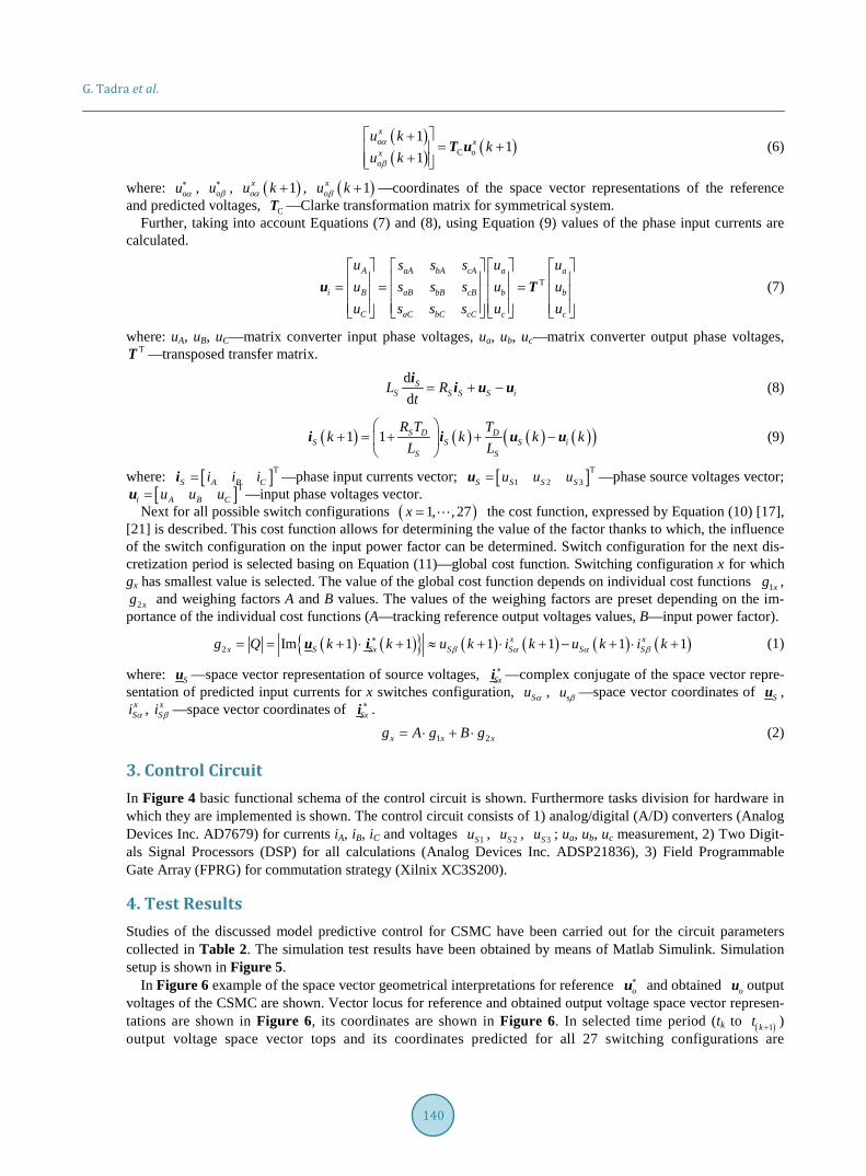
3. Control Circuit In Figure 4 basic functional schema of the control circuit is shown. Furthermore tasks division for hardware in which they are implemented is shown. The control circuit consists of 1) analog/digital (A/D) converters (Analog Devices Inc. AD7679) for currents iA, iB, iC and voltages 1Su , 2Su , 3Su ; ua, ub, uc measurement, 2) Two Digit-als Signal Processors (DSP) for all calculations (Analog Devices Inc. ADSP21836), 3) Field Programmable Gate Array (FPRG) for commutation strategy (Xilnix XC3S200).
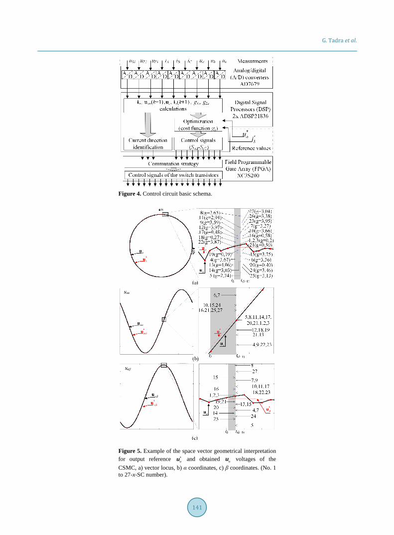
4. Test Results Studies of the discussed model predictive control for CSMC have been carried out for the circuit parameters collected in Table 2. The simulation test results have been obtained by means of Matlab Simulink. Simulation setup is shown in Figure 5.
In Figure 6 example of the space vector geometrical interpretations for reference o∗u and obtained ou output
voltages of the CSMC are shown. Vector locus for reference and obtained output voltage space vector represen-tations are shown in Figure 6, its coordinates are shown in Figure 6. In selected time period (tk to ( )1kt + ) output voltage space vector tops and its coordinates predicted for all 27 switching configurations are
G. Tadra et al.
141
Figure 4. Control circuit basic schema.
Figure 5. Example of the space vector geometrical interpretation for output reference o
∗u and obtained ou voltages of the CSMC, a) vector locus, b) α coordinates, c) β coordinates. (No. 1 to 27-x-SC number).
G. Tadra et al.
142
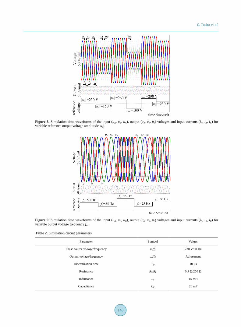
shown. It can be seen that predicted vector closest to the reference vector (with smallest g) is selected in time moment ( )1kt + . In Figure 7 for transfer ratio higher than one and three different frequencies 50 Hz, 25 Hz, 75 Hz CSMC currents and voltages’ time waveforms are presented. The response of the circuit to the output refer-ence voltage changes is shown in Figure 8. In Figure 9 the response of the circuit to the output frequency changes is presented. As it can be seen from Figure 8 and Figure 9 output voltage of the current source matrix converter under proposed model predictive control strategy reaches its reference with a very fast dynamics.
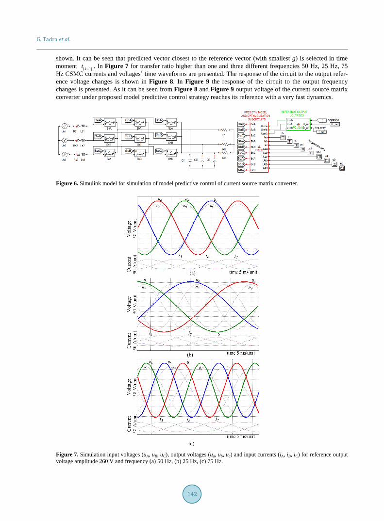
Figure 6. Simulink model for simulation of model predictive control of current source matrix converter.
Figure 7. Simulation input voltages (uA, uB, uC), output voltages (ua, ub, uc) and input currents (iA, iB, iC) for reference output voltage amplitude 260 V and frequency (a) 50 Hz, (b) 25 Hz, (c) 75 Hz.
G. Tadra et al.
143
Figure 8. Simulation time waveforms of the input (uA, uB, uC), output (ua, ub, uc) voltages and input currents (iA, iB, iC) for variable reference output voltage amplitude |uo|.
Figure 9. Simulation time waveforms of the input (uA, uB, uC), output (ua, ub, uc) voltages and input currents (iA, iB, iC) for variable output voltage frequency fo.
Table 2. Simulation circuit parameters.
Parameter Symbol Values
Phase source voltage/frequency uS/fS 230 V/50 Hz
Output voltage/frequency uO/fO Adjustment
Discretization time TD 10 µs
Resistance RS/RL 0.5 Ω/250 Ω
Inductance LS 15 mH
Capacitance CF 20 mF

G. Tadra et al.
144
5. Summary In this paper, model predictive control and a control circuit of the current source matrix converter has been pre-sented. Proposed control strategy allows obtaining output voltages with desired frequency and amplitude. Vol-tage transfer ratio for CSMC under presented control strategy can be higher than 1. Reference values are reached with fast dynamic. Furthermore, the input power factor can be controlled but it highly depends on circuit ele-ments and set parameters. Future investigations will be focused on the improvement of the input power factor control and experimental implementation of the proposed control strategy in current source matrix converter.
Acknowledgements This work was supported by the European Union, Human Capital within the project "Scholarships for PhD stu-dents studying faculties recognized as particularly important for the development of Lubuskie voivodeship", Sub-8.2.2, Action 8.2, Priority VIII.
References [1] Venturini, M. and Alesina, A. (1980) The Generalized Transformer: A New Bidirectional Sinusoidal Waveform Fre-
quency Converter with Continuously Adjustable Input Power Factor. Proceedings of the IEEE Power Electronics Spe-cialists Conference, PESC’80, Atlanta, 16-20 June 1980, 242-252.
[2] Ziogas, P.D., Khan, S.I. and Rashid, M.H. (1986) Analysis and Design of Forced Commutated Cycloconverter Struc-tures with Improved Transfer Characteristics. IEEE Transactions on Industrial Electronics, IE-33, 271-280. http://dx.doi.org/10.1109/TIE.1986.350233
[3] Huber, L. and Borojevic, D. (1989) Space Vector Modulator for Forced Commutated Cycloconverters. Conference Record of the 1989 IEEE Industry Applications Society Annual Meeting, San Diego, 1-5 October 1989, 871-876.
[4] Casadei, D., Grandi, G., Sierra, G. and Tani, A. (1993) Space Vector Control of Matrix Converters with Unity Input Power Factor and Sinusoidal Input/Output Waveforms. Fifth European Conference on Power Electronics and Applica-tions, Brighton, 13-16 September 1993, 170-175, Vol. 7.
[5] Wheeler, P.W., Rodriguez, J., Clare, J.C., Empringham, L. and Weinstein, A. (2002) Matrix Converters : A Technolo-gy Review. IEEE Transactions on Industrial Electronics, 49, 276-288. http://dx.doi.org/10.1109/41.993260
[6] Klumpner, C. and Pitic, C. (2008) Hybrid Matrix Converter Topologies: An Exploration of Benefits. Power Electron-ics Specialists Conference PESC’08, Rhodos, 15-19 June 2008, 2-8.
[7] Wijekoon, T., Klumpner, C. and Wheeler, P. (2006) Implementation of a Hybrid AC/AC Direct Power Converter with Unity Voltage Transfer Ratio. Applied Power Electronics Conference APEC’06, Dallas, 19-23 March 2006, 1478-1484.
[8] Fedyczak, Z., Szcześniak, P. and Korotyeyev, I. (2008) Generation of Matrix-Reactance Frequency Converters Based on Unipolar PWM AC Matrix-Reactance Choppers. Power Electronics Specialists Conference PESC’08, Rhodos, 15-19 June 2008, 1821-1827.
[9] Fedyczak, Z., Szcześniak, P., Kaniewski, J. and Tadra, G. (2009) Implementation of Three-Phase Frequency Conver-ters Based on PWM AC Matrix-Reactance Chopper with Buck-Boost Topology. Power Electronics and Applications EPE’09, Barcelona, 8-10 September 2009, 1-10.
[10] Szcześniak, P. (2013) Three-Phase AC-AC Power Converters Based on Matrix Converter Topology. Springer. http://dx.doi.org/10.1007/978-1-4471-4896-8
[11] Itoh, J., Koiwa, K. and Kato, K. (2010) Input Current Stabilization Control of a Matrix Converter with Boost-Up Func-tionality. International Power Electronics Conference IPEC’10, Sapporo, 21-24 June 2010, 2708-2714.
[12] Kwon, W.H. and Cho, G.H. (1993) Analyses of Static and Dynamic Characteristics of Practical Step-Up Nine-Switch Matrix Convertor. IEE Proceedings B Electric Power Applications, 140, 139-146.
[13] Nikkhajoei, H. (2007) A Current Source Matrix Converter for High-Power Applications. IEEE Power Electronics Spe-cialists Conference PESC’07, Orlando, 17-21 June 2007, 2516-2521.
[14] Fedyczak, Z., Tadra, G. and Klytta, M. (2010) Implementation of the Current Source Matrix Converter with Space Vector Modulation. Power Electronics and Motion Control Conference EPE/PEMC’10, Ohrid, 6-8 September 2010, T2-97-T2-102.
[15] Tadra, G. (2010) Układ sterowania do przekształtnika matrycowego prądu o modulacji wektorowej oraz czterostopniowej strategii komutacji. Przegląd Elektrotechniczny, No. 6, 159-162.
[16] Vasquez, S., Leon, J.I., Franquelo, L.G., Rodriguez, J., Young, H.A., Marquez, A. and Zanchetta, P. (2014) Model Predictive Control: A Review of Its Applications in Power Electronics. IEEE Industrial Electronics Magazine, 8, 16-31.

G. Tadra et al.
145
http://dx.doi.org/10.1109/MIE.2013.2290138 [17] Kouro, S., Cortés, P., Vargas, R., Ammann, U. and Rodríguez, J. (2009) Model Predictive Control—A Simple and
Powerful Method to Control Power Converters. IEEE Transactions on Industrial Electronics, 56, 1826-1838. http://dx.doi.org/10.1109/TIE.2008.2008349
[18] Rodríguez, J. and Cortes, P. (2012) Predictive Control of Power Converters and Electrical Drives. John Wiley & Sons Ltd. http://dx.doi.org/10.1002/9781119941446
[19] Rodriguez, J., Rivera, M., Kolar, W. and Wheeler, P.W. (2012) A Review of Control and Modulation Methods for Ma-trix Converters. IEEE Transactions on Industrial Electronics, 59, 58-70.
[20] Clarke, E. (1964) Circuit Analysis of AC Power Systems. John Wiley & Sons Ltd., New York. [21] Akagi, H., Watanabe, E.H. and Aredes, M. (2007) Instantaneous Power Theory and Applications to Power Conditioning.
Wiley-Interscience, A John Wiley & Sons Inc., New York.