model predictive control of power electronics converter … · · 2017-01-22model predictive...
TRANSCRIPT

Model Predictive Control of Power Electronics Converter
Jiaying Wang
Master of Science in Electric Power Engineering
Supervisor: Lars Einar Norum, ELKRAFT
Department of Electric Power Engineering
Submission date: June 2012
Norwegian University of Science and Technology


Acknowledgment First of all, I would like to thank my parents who raise me and support me to do further study in Norway. I appreciate the help from my supervisor Lars Einar Norum and Phd student Hamed Nademi. I benefit a lot from their meticulous attitude to study, abundant knowledge and minded guidance. I am very grateful that NTNU Department of Electric Power Engineering provides very good hardware resources. I would also like to thank my fellow classmates through the pleasant master-education life. Again I am cheerful that I can graduate from NTNU, a very nice university. Recalling the past two years of life in Norway, I feel very happy that I found good teachers and good friends, such as Hans, Shahbaz, Martin, Chen and so on, in the form of helping people that I will always remember. Trondheim, 12th June 2012 Jiaying Wang

2

3
Abstract Voltage-source PWM (Pulse Width Modulation) rectifier can provide constant DC bus voltage and suppress harmonic distortion of grid-side currents. It also has power feedback capability and has a broad prospect in the field of DC power supply [1], reactive power compensation, active filtering and motor control system.
This dissertation studies the theory and implementation of PWM rectifier and completes the following tasks:
1. Analyze three-phase voltage-source PWM rectifier (VSR), including its topology, mathematical model and principle. Derive Clarke transformation and Park transformation and analyze the mathematical model in the two-phase αβ stationary coordinate and dq rotating coordinate.
2. Make a detailed analysis on the principle and characteristics of Direct Power Control (DPC) strategy and Model Predictive Control (MPC) strategy and study the instantaneous active power and reactive power flow in the rectifier.
3. Based on the principle of traditional switching table of DPC, an improved table is proposed. Then this project presents a further improved switching table to achieve better control performance and the simulation model in Matlab/Simulink environment is established to verify the algorithm of voltage-oriented direct power control strategy.
4. Based on different strategy studies and the simulation results from DPC system, propose our model predictive control (MPC) algorithm.
5. Analyze the modulation principle of the space vector pulse width modulation (SVPWM).
6. Build the MPC-SVPWM model in Matlab/Simulink to verify our MPC algorithm. 7. The simulation result shows that MPC-SVPWM performs better in harmonic
suppression, unity power factor, DC output voltage ripple coefficient and dynamic response than DPC.
Key words: PWM rectifier, unity power factor, direct power control, model predictive control, harmonic suppression, SVPWM

4
5
Contents Abstract ...................................................................................................................................... 3
Contents ...................................................................................................................................... 5
Chapter 1 Introduction ............................................................................................................... 1
1.1 Background and significance of the study ....................................................................... 1
1.2 Current state of PWM converter research ........................................................................ 2
1.3 The application fields of PWM converters ....................................................................... 3
1.3.1 Active power filter and static var generator .............................................................. 3
1.3.2 Unified power flow controller ................................................................................... 4
1.3.3 Superconducting magnetic energy storage ................................................................ 4
1.3.4 Four-quadrant electrical drive ................................................................................... 4
1.3.5 Grid-connected renewable energy ............................................................................. 5
1.4 The main work of this thesis ............................................................................................ 5
Chapter 2 Three phase VSR mathematical model ...................................................................... 7
2.1 Derivation of coordinate transformation .......................................................................... 7
2.2 Principle of PWM VSR .................................................................................................... 9
2.2.1 Mathematical model in αβ stationary coordinate system ........................................ 12
2.2.2 Mathematical model in dq rotating coordinate system ........................................... 13
Chapter 3 Principle of Direct power control ............................................................................ 15
3.1 Power theory and calculation of instantaneous power ................................................... 15
3.2 Voltage-oriented direct power control of PWM VSR .................................................... 16
3.2.1 System composition of VSR ................................................................................... 16
3.2.2 Principle of DPC ..................................................................................................... 17
3.3 Power flow in the converter ........................................................................................... 25
Chapter 4 Principle of Model predictive control ...................................................................... 28
4.1 Review of MPC in power converters ............................................................................. 29
4.2 Process, model and controller of VSR ........................................................................... 30
4.3 Two-level SVPWM modulation technique .................................................................... 32
4.3.1 Voltage space vector distribution of three-phase VSR ............................................ 32
4.3.2 Synthesis of voltage space vector ............................................................................ 34
Chapter 5 Simulation ................................................................................................................ 37
5.1 Simulation of direct power control system .................................................................... 37
5.1.1 Comparison of different switching tables ............................................................... 38
5.1.2 Dynamic response of DPC ...................................................................................... 42
5.1.3 Summary ................................................................................................................. 45
5.2 Simulation of model predictive control .......................................................................... 46
5.2.1 Startup and steady state ........................................................................................... 48

6
5.2.2 Dynamic performance of MPC-SVPWM ............................................................... 50
5.2.3 Summary ................................................................................................................. 63
Chapter 6 Conclusion and future work .................................................................................... 64
6.1 Conclusions from the Simulink results .......................................................................... 64
6.2 Suggested future work .................................................................................................... 64
Appendix .................................................................................................................................. 65
Deviation of power supply voltages in dq frame ed and eq .................................................. 65
Switching function waveforms in six sectors ....................................................................... 65
Codes in Embedded MATLAB Function ............................................................................. 67
References ................................................................................................................................ 72
1
Chapter 1 Introduction
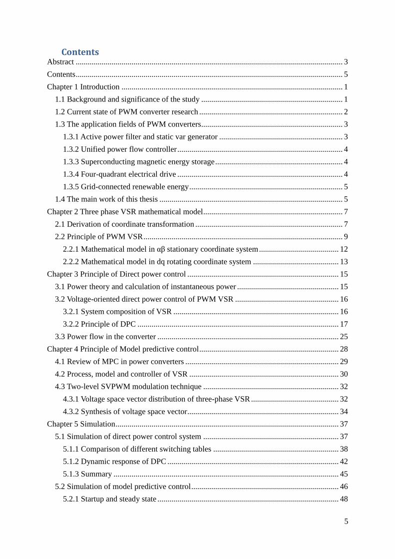
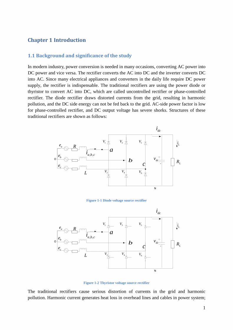
1.1 Background and significance of the study In modern industry, power conversion is needed in many occasions, converting AC power into DC power and vice versa. The rectifier converts the AC into DC and the inverter converts DC into AC. Since many electrical appliances and converters in the daily life require DC power supply, the rectifier is indispensable. The traditional rectifiers are using the power diode or thyristor to convert AC into DC, which are called uncontrolled rectifier or phase-controlled rectifier. The diode rectifier draws distorted currents from the grid, resulting in harmonic pollution, and the DC side energy can not be fed back to the grid. AC-side power factor is low for phase-controlled rectifier, and DC output voltage has severe shorks. Structures of these traditional rectifiers are shown as follows:
ae
be
ce
R
LR, ,a b ci
L
O
b
-dcv
dci
Lia
b c
1V 3V 5V
2V 4V 6V
Figure 1-1 Diode voltage source rectifier
ae
be
ce
R
LR, ,a b ci
L
O
b
-dcv
dci
Lia
b c
1V 3V 5V
2V 4V 6V
Figure 1-2 Thyristor voltage source rectifier
The traditional rectifiers cause serious distortion of currents in the grid and harmonic pollution. Harmonic current generates heat loss in overhead lines and cables in power system;

2
harmonic currents flowing in the overhead line will cause serious electromagnetic interference to adjacent communication equipment and interfere with the protection devices and cause malfunction; harmonic currents cause dielectric loss in power capacitors and speed up aging; much reactive power exchanges with the grid, producing large amount of additional energy losses. These factors restrict its application in industry.
The most fundamental way to solve this harmonic pollution is to make the converter produce no harmonics and realize the sinusoidal current in the grid side and unity power factor. With the development of power electronics, the advanced full-controlled power semiconductor devices and microprocessor technology and control theories promote the development of the converter. A variety of converters emerge based on pulse width modulation control. Voltage-source PWM rectifier (VSR) has the following advantages: low harmonics of the currents in the grid side, unity power factor, constant DC voltage and bi-directional energy flow.
With certain topology of main circuit, to achieve the above advantages of VSR, various control strategies have been proposed. Turn off and on the fully-controlled power devices in accordance with a certain control strategy, we can control the magnitude and phase angle of AC currents, supplying appropriate power to the load and AC currents close to sinusoidal waveform, in phase with supply voltages. Then the power factor will be close to unity, achieving the purpose to improve power factor and to suppress harmonics. The significance of improvement of power factor on the actual production is enormous. For example, in a 10,000 ton-class chemical plant, DC current is needed to electrolyze the saline solution to produce the most basic raw materials for the chemical industry: chlorine gas and sodium hydroxide. In this energy-intensive industry, if the power factor can be increased by a few percentage points, a very considerable part of electric energy can be saved. PWM converter can work in four quadrants due to its fully-controlled switching devices (referring to chapter 2.2), so that energy can be fed back into the supply grid when the motor works in regenerate mode.
1.2 Current state of PWM converter research PWM rectifier research began in the 1980s, when the self-turn-off devices became mature, promoting the application of the PWM technique. In 1982 Busse Alfred and Holtz Joachim proposed the three-phase full-bridge PWM rectifier topology based on self-turn-off devices and the grid-side current amplitude and phase control strategy [2], and implemented unity power factor and sinusoidal current control of the current-source PWM rectifier. In 1984, Akagi Hirofumi with others proposed reactive power compensation control strategy based on the PWM rectifier topology [3], which was actually the early idea of voltage-source PWM rectifier. At the end of the 1980s, Green A.W proposed continuous and discrete dynamic mathematical models and control strategy of PWM rectifier based on coordinate transformation, raising PWM rectifier research and development to a new level [4]. PWM rectifier according to the output can be divided into the voltage-source and current-source rectifier. For a long time, the voltage-source PWM rectifier (VSR) for its low losses, simple structure and control strategy has become the focus of the study of PWM rectifier, while the current-source PWM rectifier (CSR) is relatively complex due to the presence of DC energy-storage inductor and AC LC filter inductor. Voltage-source inverter has a similar topology with VSR but operating in opposite direction. The main power converter that is
3
investigated in this work is VSR. There are several control strategies: current control (including indirect current control and direct current control) and nonlinear control strategy (including instantaneous power control, feedback linearization control, Lyapunov control and so on). Indirect current control strategy controls grid currents indirectly by controlling the amplitude and phase angle of the fundamental component of input voltage of rectifier. However, this strategy has some disadvantages: bad stability, slow dynamic response and current overshoot in dynamic process, restricting its application [5]. Direct current control strategy controls AC current directly by following the given reference current. The typical example is the dual-loop PI control. This strategy with fast dynamic response uses space vector modulation, increases the utilization of DC voltage and has been applied in practical projects. PWM converter has the following characteristics: nonlinear, multivariable and strong coupling. Its traditional control algorithms adopt linearization based on small signal disturbance on steady operating point, which may not maintain the stability of large range disturbances. So some proposed control strategy based on Lyapunov stability theory. This novel control scheme builds the Lyapunov function based on the quantitative relationship of inductor and capacitor energy storage. The Lyapunov function combines the PWM mathematical model in dq rotating frame and corresponding SVPWM constraints to deduce the control algorithm. This control strategy solves the stability issue of large range disturbances [6]. To increase the performance of PWM VSR, research on nonlinear control method and new control algorithm is a new challenge for the reseachers now.
1.3 The application fields of PWM converters The AC side of PWM rectifier has a characteristic of controlled current source, which makes the development of the control strategies and topologies of PWM rectifier. Power converter are used in many fields, such as static var generator (SVG), active power filter (APF), unified power flow controller (UPFC), superconducting magnetic energy storage (SMES), high voltage direct current transmission (HVDC), electrical drive and grid-connected renewable energy [7].
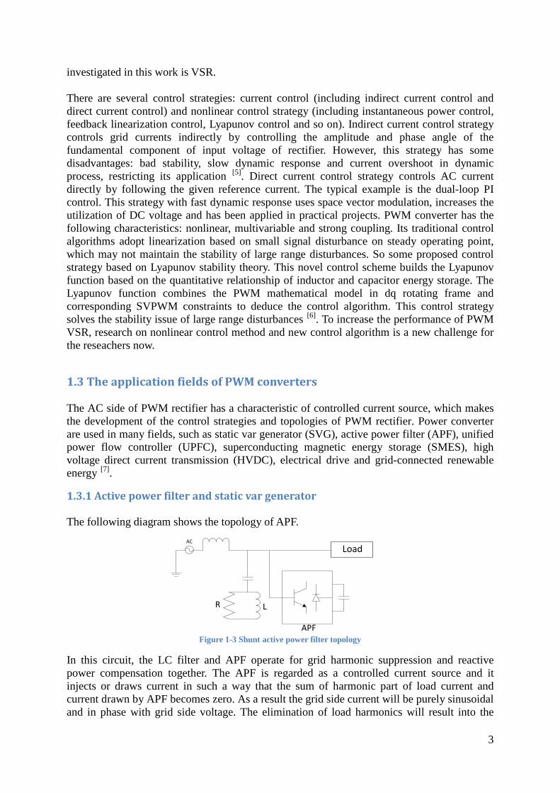
1.3.1 Active power filter and static var generator The following diagram shows the topology of APF.
ACLoad
R L
APF Figure 1-3 Shunt active power filter topology
In this circuit, the LC filter and APF operate for grid harmonic suppression and reactive power compensation together. The APF is regarded as a controlled current source and it injects or draws current in such a way that the sum of harmonic part of load current and current drawn by APF becomes zero. As a result the grid side current will be purely sinusoidal and in phase with grid side voltage. The elimination of load harmonics will result into the

4
improvement of reactive power control as well [8].
1.3.2 Unified power flow controller The UPFC is the most promising power compensation device in flexible alternating current transmission system. UPFC is used in the transmission grid, controlling active power flow and absorbing or supplying reactive power. UPFC consists of combination of series active power filter and shunt active power filter. The series APF is equivalent to a controlled voltage source, compensating high frequency components of grid voltage, zero sequence component and negative sequence component of fundamental component of grid voltage; while shunt APF is equivalent to an APF, a controlled current source, absorbing or supplying reactive power. Its topology is shown as follows:
AC
Grid
Figure 1-4 UPFC topology
1.3.3 Superconducting magnetic energy storage SMES is mainly used for peak load regulation control, and other occasions where short-time compensation of electrical energy is needed. When current consumption of electricity is normal, the electricity in the grid is converted into energy in superconducting coils through converter to store enough energy. During large power consumption, the energy in the superconducting coil is fed to the grid through the converter, in order to achieve the purpose of peak load regulation. Its topology is shown as follows:
GridSuperconductingcoil
Figure 1-5 SMES topology
The main circuit of SMES is usually composed by current-source PWM rectifier. The lossless superconducting coil is connected in series with the DC side of PWM rectifier. The coil itself is both a DC buffer inductor and load of the DC side. This design simplifies the structure of main circuit of current-source rectifier, and overcomes the shortcoming—the large loss of conventional current-source rectifier.
1.3.4 Four-quadrant electrical drive PWM rectifier replaces the diode rectifier, eliminates the energy dissipation device at the DC side of inverter, achieves steady DC voltage at the DC side of rectifier and enhances the actuating performance of motor. On the other hand, appropriate control strategy can reduce
5
the capacitance of the DC side capacitor. The four-quadrant electrical drive topology is shown as follows:
AC
rectifier
M
inverter
Figure 1-6 Four-quadrant electrical drive topology
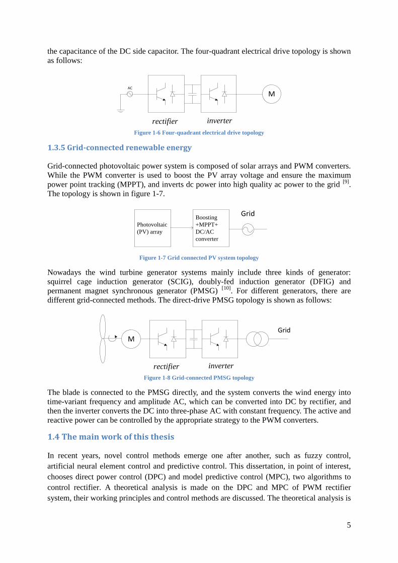
1.3.5 Grid-connected renewable energy Grid-connected photovoltaic power system is composed of solar arrays and PWM converters. While the PWM converter is used to boost the PV array voltage and ensure the maximum power point tracking (MPPT), and inverts dc power into high quality ac power to the grid [9]. The topology is shown in figure 1-7.
GridPhotovoltaic(PV) array
Boosting+MPPT+DC/AC converter
Figure 1-7 Grid connected PV system topology
Nowadays the wind turbine generator systems mainly include three kinds of generator: squirrel cage induction generator (SCIG), doubly-fed induction generator (DFIG) and permanent magnet synchronous generator (PMSG) [10]. For different generators, there are different grid-connected methods. The direct-drive PMSG topology is shown as follows:
rectifier
M
inverter
Grid
Figure 1-8 Grid-connected PMSG topology
The blade is connected to the PMSG directly, and the system converts the wind energy into time-variant frequency and amplitude AC, which can be converted into DC by rectifier, and then the inverter converts the DC into three-phase AC with constant frequency. The active and reactive power can be controlled by the appropriate strategy to the PWM converters.
1.4 The main work of this thesis In recent years, novel control methods emerge one after another, such as fuzzy control, artificial neural element control and predictive control. This dissertation, in point of interest, chooses direct power control (DPC) and model predictive control (MPC), two algorithms to control rectifier. A theoretical analysis is made on the DPC and MPC of PWM rectifier system, their working principles and control methods are discussed. The theoretical analysis is
6
checked through simulation and at the end some conclusions are drawn. The main content is as follows:
1. The first chapter describes that developing PWM rectifier becomes an important way to solve the harmonic pollution and analyzes the status of PWM rectifier technology, introduces some new PWM rectifier control strategies, and finally introduces the applications of PWM rectifier in different fields.
2. In the first half of second chapter, the derivation of coordinate transformation is done and in the second of the working principle of the PWM rectifier and its mathematical model in different coordinate systems are discussed.
3. The third chapter analyzes the power control theory, the principle of direct power control strategy and fundamentals of the traditional switching table and the components of direct power control system, and improves the traditional switching table.
4. The fourth chapter focuses on the principle of model predictive control, and gives the mathematical prediction model of VSR.
5. The fifth chapter simulates the direct power control and model predictive control strategy in the Matlab/Simulink environment, respectively, and simulation results are compared and analyzed in detail. It draws the conclusion that model predictive control of PWM rectifier performs better and MPC of VSR has the following advantages: unity power factor, small AC current harmonics, and small DC voltage ripple coefficient.
6. The content of the research is summarized and forecasted in the last chapter, mainly summarizing the fulfillment of this project, conclusion and next-stage working plan.
7
Chapter 2 Three phase VSR mathematical model This chapter mainly analyzes mathematical model of voltage-source rectifier, and then describes its operating principle in favor of establishing simulation model in Simulink. In the beginning of this chapter, the coordinate transformations namely Clarke transformation and Park transformation which are used in building the mathematical model are formulated briefly [11].
2.1 Derivation of coordinate transformation Derivation of the coordinate theory includes: abc stationary coordinate to αβ stationary coordinate system, abc stationary coordinate system to dq rotating coordinate system. There are two standards for transformation: power invariance and amplitude invariance. In this paper, power invariance is used in the modeling of direct power control. The following figure shows the relationship of different coordinate systems.
a
θ
ωc
b
axisa −
axisb −
d axis−
q axis−
dx
Figure 2-1 Relationship of coordinates
In the beginning the amplitude invariant transformation is introduced. The amplitude invariant coordinate transformation is that one common vector of one coordinate system is equal to another common vector of other coordinate system. Power invariant transformation refers to coordinate transformation before and after, the power does not change. The general vector x will be taken for example to discuss two standards of coordinate transformation.
1 abc-αβ transformation
We use a set of orthogonal αβ axes affixed where α-axis is aligned with the a-axis. The angle between x and α is δ. The projection of vector x along the abc-axis is obtained:
8
coscos( 2 / 3)cos( 2 / 3)
a m
b m
c m
x xx xx x
dd πd π
= ⋅ = ⋅ − = ⋅ +
(2.1)
Where xm is the magnitude of vector x. The projection of vector x along the αβ-axis is as follows:
2 2
cossin
m
m
m
x xx x
x x x
a
b
a b
dd
= ⋅ = ⋅ = +
(2.2)
We know the following trigonometric relations:
2 1 1cos cos cos( 2 / 3) cos( 2 / 3)3 2 23 32sin cos( 2 / 3) cos( 2 / 3)3 2 2
d d d π d π
d d π d π
= − − − + = − − +
(2.3)
Combining the equations (2.1) (2.2) (2.3), we got
2 1 1( )3 2 2
3 32 ( )3 2 2
a b c
b c
x x x x
x x x
a
b
= − − = −
(2.4)
Set zero-axis component 1 ( )3o a b cx x x x= + + we got,
1 112 2
2 3 303 2 2
1 1 12 2 2
a
b
co
x xx x
xx
a
b
− − = −
(2.5)
2 abc-dq transformation
The outstanding advantage of dq transformation is that the fundamental sinusoidal variables are transformed into DC variables. In three-phase stationary abc coordinate system, e and i represent grid emf vector and current vector respectively, and rotate with speed of ɷ (fundamental angular frequency) in anticlockwise direction. When describing the three-phase electrical parameters, to simplify the analysis, the d-axis of the two-phase rotating reference frame aligns with the grid emf vector e.
As shown in figure 2-1, the angle between vector x and α-axis is δ and the angle between d-axis and α-axis is θ, the projection of vector x along the dq-axis will be:

9
2 2
cos( )sin( )
d m
q m
m d q
x xx x
x x x
θ dd θ
= ⋅ − = ⋅ − = +
(2.6)
We know the following trigonometric relations:
[ ][ ]
2cos( ) cos cos cos( 2 / 3)cos( 2 / 3) cos( 2 / 3)cos( 2 / 3)32sin( ) sin cos sin( 2 / 3)cos( 2 / 3) sin( 2 / 3)cos( 2 / 3)3
θ d d θ θ π d π θ π d π
θ d θ d θ π d π θ π d π
− = + − − + + +
− = + − − + + +
(2.7)
Also set zero-axis component 1 ( )3o a b cx x x x= + + we got,
cos cos( 2 / 3) cos( 2 / 3)
2 sin sin( 2 / 3) sin( 2 / 3)3
1 1 12 2 2
d a
q b
co
x xx x
xx
θ θ π θ πθ θ π θ π
− + = − − − − +
(2.8)
Transformation matrix in the equations (2.5) and (2.8) is not orthogonal matrix, which makes matrix operations difficult. So power invariant transformation is raised as follows:
1 112 2
2 3 303 2 2
1 1 12 2 2
a
b
co
x xx x
xx
a
b
− − = −
(2.9)
cos cos( 2 / 3) cos( 2 / 3)
2 sin sin( 2 / 3) sin( 2 / 3)3
1 1 12 2 2
d a
q b
co
x xx x
xx
θ θ π θ πθ θ π θ π
− + = − − − − +
(2.10)
2.2 Principle of PWM VSR The main circuit topology of three-phase voltage-source PWM rectifier is shown in figure 2-2 [12], which is the most common topology. The project studies various control strategies based on this three-phase half-bridge topology.
10
ae
be
ce
R
LR, ,a b ci
L
O
b
-dcv
dci
Li
ab c
as
1V 3V5V
2V 4V 6V
csbs
Figure 2-2 Topology of three-phase PWM rectifier
, ,a b ce e e e= are the three-phase power supply phase voltages, , ,a b ci i i i= are the three-phase currents. V1-V6 are the power electronic devices, for example, IGBT and diode. L is inductance of the filter and R is the sum of resistance of filter and equivalent resistance of the switch power losses. RL is the load resistance. The inductor of the filter suppresses harmonics in AC currents and boosts the output voltage of VSR. , ,r ao bo cov v v v= are the input voltages of VSR. Current i is controlled by the difference of power supply e and input voltage vr if we neglect the influence of voltage across R. Since e is given, i is determined by vr. If the amplitude and phase of vr can be controlled, then the amplitude and phase of i can be controlled accordingly. It can operate in four quadrants, and its vector diagram is shown as follows:
ei
rv
Rv
Lve
e
e
i
i
i
rectifier
Lv
Lv
LvRv
Rv
Rv
rv
rv
rv
inverter
capacitance characteristics inductance characteristics
)a )b
)c )d
Figure 2-3 Four-quadrant vector diagram
In figure 2-3 a), i is in phase with e, and it’s in unity power factor rectifier mode. In b), the circuit operates as an inverter, achieving the feedback of energy. In c), the converter does not absorb active power from the grid, and only absorbs the capacitive reactive power from the grid. In d), the converter does not absorb active power from the grid, and only absorbs inductive reactive power from the grid. By controlling the vector vr, the PWM VSR can operate in any position of the four quadrants.

11
, ,a b cs s s are switching function of the power converter. Unipolar binary logic switch function is defined as follows:
1
(k ,b,c)0ks a
= =
(2.11)
1ks = means that upper switch is on and 0ks = means lower switch is on. Our mathematical model is derived based on this switching function, and since it does not neglect the role of high-frequency component, this model reflects the operation mechanism. It can be used to get the high-accuracy dynamic simulation. It is also helpful for the implementation of the physical hardware circuit. In the equivalent mathematical model, conduction voltage drop and switching losses of the switching devices are excluded, and AC side inductor saturation is excluded as well. Three- phase balanced power supply voltages are given:
2 cos
2 cos( 2 / 3)
2 cos( 2 / 3)
a m
b m
c m
e U t
e U t
e U t
ω
ω π
ω π
= = −
= +
(2.12)
Where Um is the Root-Mean-Square value of grid phase to phase voltage. Apply Kirchhoff's voltage law on the AC side of rectifier, and we got the circuit equation of phase A,
0( )aa a aN N
diL Ri e v vdt
+ = − + (2.13)
When V1 is on and V2 is off, Sa =1, aN dcv v= ; when V1 is off and V2 is on, Sa =0, 0aNv = . It means aN dc av v s= . We can also get equations of phase B and C in the same way,
0
0
( )
( )
bb b dc b N
cc c dc c N
diL Ri e v s vdtdiL Ri e v s vdt
+ = − + + = − +
(2.14)
In three-phase neutral system, the sum of three-phase currents is zero. 0a b ci i i+ + = (2.15)
For three-phase balanced grid voltage, we got 0a b ce e e+ + = (2.16)
Adding the left side and right side of equations (2.13) (2.14) respectively, we got
0 ( )3dc
N a b cvv s s s= − + + (2.17)
In addition, apply Kirchhoff's current law at DC capacitor positive node, we got

12
dcdc L
dvC i idt
= − (2.18)
Where dc a a b b c ci i s i s i s= + + and for resistive load, L dc Li v R= . By solving equations (2.13), (2.14) and (2.18), we got the general mathematical model of three-phase VSR under the three-phase stationary abc coordinate system:
( )3
( )3
( )3
a a b ca a a dc
b a b cb b b dc
c a b cc c c dc
dc dca a b b c c
L
di s s sL e Ri s vdtdi s s sL e Ri s vdtdi s s sL e Ri s vdtdv vC i s i s i sdt R
+ + = − − −
+ + = − − − + + = − − −
= + + −
(2.19)
The physical meaning of this mathematical model is clear, yet the variables in AC side are time-varying quantities, which is inconvenient to design the control system. Therefore, coordinate transformation is used.
2.2.1 Mathematical model in αβ stationary coordinate system Since we have two standards of coordinate transformation, we will list both. Amplitude invariant transformation:
( )32
dc
dc
dcL
diL e Ri v sdtdi
L e Ri v sdt
dvC i s i s idt
aa a a
bb b b
a a b b
= − − = − −
= + −
(2.20)
Power invariant transformation:
( )
dc
dc
dcL
diL e Ri v sdtdi
L e Ri v sdt
dvC i s i s idt
aa a a
bb b b
a a b b
= − − = − −
= + −
(2.21)
The mathematical model structure of VSR under αβ stationary coordinate is shown as follows:

13
⊕1
R sL+ea
⊗
+
−
sa
⊗ia
⊕1
R sL+eb
⊗
+
−
sb
⊗ib
⊕+
+⊕+−
Li1
sCdcv
Figure 2-4 Structure of VSR in stationary frame
It can be seen from above figure that if vdc is constant, there is no coupling between i and ia b in αβ stationary frame. However, the voltages ,e ea b and the currents ,i ia b are still sinusoidal variations, which are complex to control. To solve this problem, the model in dq rotating coordinate frame is built.
2.2.2 Mathematical model in dq rotating coordinate system Amplitude invariant transformation:
3 ( )2
dd q d dc d
qq d q dc q
dcd d q q L
diL e Li Ri v sdtdi
L e Li Ri v sdtdvC i s i s idt
ω
ω
= + − − = − − −
= + −
(2.22)
Power invariant transformation:
( )
dd q d dc d
qq d q dc q
dcd d q q L
diL e Li Ri v sdtdi
L e Li Ri v sdtdvC i s i s idt
ω
ω
= + − − = − − −
= + −
(2.23)
The mathematical model structure of VSR under dq rotating coordinate is shown as follows:

14
⊕1
R sL+de
⊗
+−
ds
⊗di
⊕1
R sL+qe
⊗
+−
qs
⊗qi
⊕+
+⊕+−
Li1
sCdcv
Lω−
Lω
+
−
Figure 2-5 Structure of VSR in rotating frame
There is coupling between d qi and i in dq rotating frame. Coupling terms make complexity in the design of control system, so the decoupling control is needed.

15
Chapter 3 Principle of Direct power control From the energy point of view, when AC voltage is given, if the instantaneous power of PWM rectifier can be controlled within the allowable range, the instantaneous current within the allowable range can be controlled indirectly, and such control strategy is the direct power control (DPC). In the early 1990s, Tokuo Ohnishi proposed a new control strategy using instantaneous active and reactive power in a closed loop control system of PWM converter, and then Toshihiko Noguchi and other scholars studied and made progress. Structure of DPC rectifier system contains the DC voltage outer loop and power control inner loop, and it selects switches in the switching table according to the AC-side instantaneous power, to achieve low total harmonic distortion (THD), high power factor, simple algorithm and fast dynamic response.
3.1 Power theory and calculation of instantaneous power To study the direct power control strategy of VSR, instantaneous power theory is used to calculate the instantaneous values of active and reactive power. Instantaneous values of three-phase voltages and three-phase currents are a b c a b cu u u and i i i respectively. After Clarke transformation, we can get voltages u ua b and currents i ia b under two-phase αβ coordinate system.
(1) Three-phase abc stationary coordinate In the three-phase circuit, instantaneous phase to phase voltages and the instantaneous phase currents can compose the instantaneous voltage vector u and current vector i in the Cartesian coordinate abc system. [ ]T
a b cu u u u= (3.1)
[ ]Ta b ci i i i= (3.2)
Instantaneous active power is the scalar product while instantaneous reactive power is the vector product. So we got, a a b b c cp u i u i u i u i= ⋅ = + + (3.3)
1 [( ) ( ) ( ) ]3 b c a c a b a b cq u i u u i u u i u u i= × = − + − + − (3.4)
(2) Two-phase stationary αβ coordinate For power invariant transformation, we got
3 2 3 2, ( ), , ( )2 2 2 2a b c a b ci i i i i u u u u ua b a b= = − = = − (3.5)
From equations (3.3) (3.4) and (3.5), the formula of power can be expressed as follows:
16
p u i u i u iq u i u i u i
a a b b
b a a b
= ⋅ = + = × = −
(3.6)
So similarly, we could find formula of power in dq coordinate system. (3) Two-phase dq rotating coordinate
d d q q
q d d q
p u i u iq u i u i= +
= − (3.7)
For a three-phase balanced power system, we have
3 , 0d m q
d d
d q
u U u
p u iq u i
= =
= = −
(3.8)
Where Um is the Root-Mean-Square value of grid phase to phase voltage. Power factor is cosλ ϕ= , and ϕ is the phase difference between the voltage and current when the voltage and current are sinusoidal quantities. However, the phase difference between the instantaneous voltage vector and instantaneous current vector is not constant in the process of instantaneous power adjustment. We can use instantaneous power method to calculate the power factorλ ,
2 2
pp q
λ =+
(3.9)
3.2 Voltage-oriented direct power control of PWM VSR Take the angle of the rotating vector of the grid voltage as the reference angle of the controller and then determine all the vectors’ position in the reference coordinate system, eventually control the phase angle of the AC current. It is called voltage orientation control and this control scheme needs to obtain the accurate phase angle of the grid voltage, usually obtained by the direct detection of the grid voltage. Voltage-Oriented direct power control strategy uses two options: with AC voltage sensors and without AC voltage sensors [13], calculates the instantaneous active and reactive power of the rectifier in real-time, compares them with a given active and reactive power, and finally gives commands to keep the instantaneous power as well as the instantaneous current in allowed limits. This report only covers AC voltage sensor strategy.
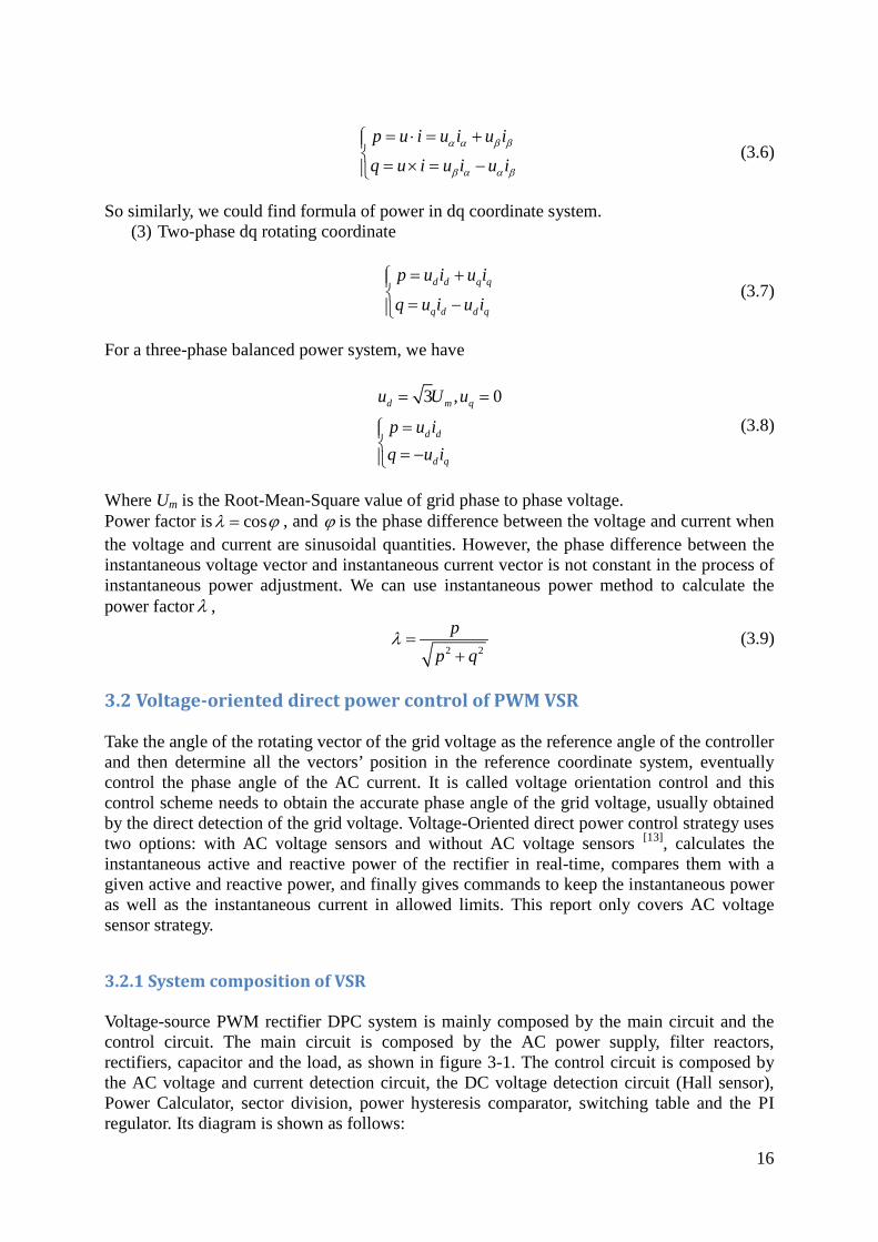
3.2.1 System composition of VSR Voltage-source PWM rectifier DPC system is mainly composed by the main circuit and the control circuit. The main circuit is composed by the AC power supply, filter reactors, rectifiers, capacitor and the load, as shown in figure 3-1. The control circuit is composed by the AC voltage and current detection circuit, the DC voltage detection circuit (Hall sensor), Power Calculator, sector division, power hysteresis comparator, switching table and the PI regulator. Its diagram is shown as follows:
17
Figure 3-1 DPC block diagram
3.2.2 Principle of DPC
1. Calculation of power We can use mathematical model in αβ stationary coordinate system and equation (3.6) to calculate instantaneous active power and reactive power.
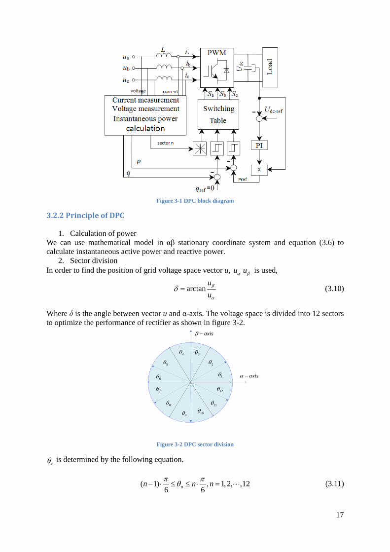
2. Sector division In order to find the position of grid voltage space vector u, u ua b is used,
arctanuub
a
d = (3.10)
Where δ is the angle between vector u and α-axis. The voltage space is divided into 12 sectors to optimize the performance of rectifier as shown in figure 3-2.
1θ axisa −
axisb −
2θ3θ4θ
5θ
6θ
7θ
8θ
9θ 10θ
12θ
11θ
Figure 3-2 DPC sector division
nθ is determined by the following equation.
( 1) , 1, 2, ,126 6nn n nπ πθ− ⋅ ≤ ≤ ⋅ = ⋅⋅⋅ (3.11)

18
3. Power hysteresis comparator The input of two hysteresis comparators are the difference ∆𝑝 = 𝑝𝑟𝑟𝑟 − 𝑝 of given value of active power and actual value of active power and the difference ∆𝑞 = 𝑞𝑟𝑟𝑟 − 𝑞 of given value of reactive power and actual value of reactive power. 𝑝𝑟𝑟𝑟 is set by the product of the PI regulator output and DC output voltage; 𝑞𝑟𝑟𝑟 is set to be zero to achieve unity power factor. The output of hysteresis comparators reflects the deviation of actual power from given power. The power hysteresis comparator can be implemented by Schmitt circuit or software. We define the following state values which reflect the deviation of actual power from given power.
1,
0,
1,
0,
ref pp
ref p
ref qq
ref q
p p HS
p p H
q q HS
q q H
< −= > +< −= > +
(3.12)
When the input of hysteresis comparator exceeds positive hysteresis band width Hp or Hq, the output is 1, which means that the driving signals of PWM through modulation should increase the power of rectifier. When the input is lower than negative hysteresis band width –Hp or –Hq, the output is zero and the driving signals of PWM which will decrease the power of rectifier should be chosen. When the input of comparator is between -H and +H, the output will be the output of previous cycle. The values of Hp and Hq have an important impact on the harmonic current and switching frequency and power tracking capability. Based on equation (3.12), if the active power or reactive power amplitude is not in their desired range, the selection of switches is made. The logic of selection is mentioned in chapter 3 table 3-1 and the comparator model is drawn as follows:
Figure 3-3 Power hysteresis comparators
Power hysteresis band affects the control precision of instantaneous power, DC voltage and AC currents. From equation (3.6), there is cross coupling between the control of active and reactive power. When the control system operates at border region of two sectors, wrong switches can be chosen easily and with big hysteresis band, duration time of wrong switches is long. It reveals that with a larger band, the power can vary over a larger range yet increasing the instantaneous power ripple, DC voltage ripple and AC current distortion, which is bad for converter and load. Some negative impact on performance of DPC is inevitable with big ,p qH H . With small hysteresis band, the switch frequency increases and losses of switches increase as well.
2sq
1sp
Relay1
Relay
4P
3P'
2Q
1Q'
19
Another important issue in DPC is the PI controller. The proportional gain and integral gain also have significant impact on the performance of DPC. Usually these gains are obtained by trial and error.
4. Switching table Rewrite the first two equations in (2.21), and we got
dc
r
dc
diL e Ri v sdidt L e Ri v
di dtL e Ri v s
dt
aa a a
bb b b
= − − ⇒ = − − = − −
(3.13)
Where , ,a r dc dce e je i i ji v v s jv sb a b a b= + = + = + . If the impact of R is neglected, we got
0
1(0) ( )T
r rdiL e v i i e v dtdt L
= − ⇒ = + −∫ (3.14)
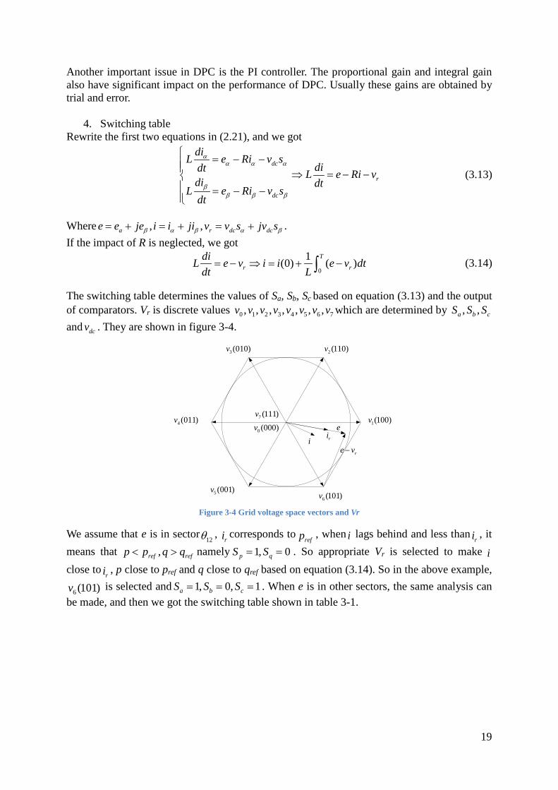
The switching table determines the values of Sa, Sb, Sc based on equation (3.13) and the output of comparators. Vr is discrete values 0 1 2 3 4 5 6 7, , , , , , ,v v v v v v v v which are determined by , ,a b cS S Sand dcv . They are shown in figure 3-4.
1(100)v
2 (110)v3 (010)v
4 (011)v
5 (001)v6 (101)v
7 (111)v
0 (000)v
re v−
e
i ri
Figure 3-4 Grid voltage space vectors and Vr
We assume that e is in sector12θ ,
ri corresponds torefp , when i lags behind and less than
ri , it means that ,ref refp p q q< > namely 1, 0p qS S= = . So appropriate Vr is selected to make iclose to
ri , p close to pref and q close to qref based on equation (3.14). So in the above example,
6 (101)v is selected and 1, 0, 1a b cS S S= = = . When e is in other sectors, the same analysis can be made, and then we got the switching table shown in table 3-1.

20
Table 3-1 DPC improved switching table
pS qS , ,a b cS S S
1θ 2θ 3θ 4θ 5θ 6θ 7θ 8θ 9θ 10θ 11θ 12θ 1 0 101 100 100 110 110 010 010 011 011 001 001 101 1 1 110 010 010 011 011 001 001 101 101 100 100 110 0 0 100 100 110 110 010 010 011 011 001 001 101 101 0 1 110 110 010 010 011 011 001 001 101 101 100 100
The classical switching table is presented in the following:
Table 3-2 DPC classical switching table
pS qS , ,a b cS S S
1θ 2θ 3θ 4θ 5θ 6θ 7θ 8θ 9θ 10θ 11θ 12θ 1 0 111 100 000 110 111 010 000 011 111 001 000 101 1 1 111 000 000 111 111 000 000 111 111 000 000 111 0 0 100 100 110 110 010 010 011 011 001 001 101 101 0 1 110 110 010 010 011 011 001 001 101 101 100 100
In the classical switching table, extensive use of vectors V0 and V7 weakens the control of reactive power. Zero vectors can increase active power but the capability is weak. Its main purpose is to reduce the switching frequency. The average switching frequency of classical switching table is low, which is an advantage. Compared with classical table, this improved switching table improves its ability to regulate the reactive power; however the area exists where active power is out of control. See the figure below for specific analysis.
e axisa −
axisb −
2θ3θ4θ
5θ
6θ
7θ
8θ
9θ 10θ
12θ
11θ
2v
Figure 3-5 Analysis of uncontrollable area
When e is in sector1θ and 1, 1p qS S= = . According to the switching table, V2 is selected. When
e is the green line, V2 is correct. The vector angle between vector e and vector (e-vr) is acute angle, which increases i and decreases the angle between ir and i. However, when e is the purple line, the vector angle between vector e and vector (e-vr) is obtuse angle, which decreases i and decreases the angle between ir and i. V2 makes the active power even less. The size of the uncontrollable area is determined by the ratio of radius of two circles:

21
3 3
223
m m
r dcdc
Ue Uv vv
= = (3.15)
In the following, we will derive a new switching table, where the best basic voltage vector Vr in each sector is selected. This table is synthesized by analyzing the change in the active and reactive power [14]. Adopt the discrete first order approximation on equation (3.13) and neglect the impact of R, and we got the change of current vectors,
( 1) ( ) ( ( ) ( ))
( 1) ( ) ( ( ) ( ))
dc
dc
Ti i k i k e k v s kLTi i k i k e k v s kL
a a a a a
b b b b b
∆ = + − = −∆ = + − = −
(3.16)
Where 1/T is the sampling frequency. Rewrite the equation (3.6), and the instantaneous power can be expressed as follows:
p u i e i e iq u i e i e i
a a b b
b a a b
= ⋅ = + = × = −
(3.17)
We assume that ,e ea b are constant in one sampling period due to the high switching frequency. So the changes of power in next period can be estimated by:
[ ][ ]
( 1) ( ) ( 1) ( )
( 1) ( ) ( 1) ( )
p e i k i k e i k i k
q e i k i k e i k i ka a a b b b
b a a a b b
∆ = + − + + −
∆ = + − − + − (3.18)
Substituting ,i ia b∆ ∆ in equation (3.16) for equation (3.18), we got changes of active power and reactive power in the next period ( 1) ( ), ( 1) ( )p p k p k q q k q k∆ = + − ∆ = + − ,
2 2( ) ( ) ( ) ( ) ( )
( ) ( ) ( ) ( )
dc dc
dc dc
T Tp e e e k v s k e k v s kL LTq e k v s k e k v s kL
a b a a b b
a b b a
∆ = + − − ∆ = −
(3.19)
For power invariant transformation, we got,
3 cos
3 sinm
m
e U
e Ua
b
θ
θ
=
= (3.20)
For the basic vectors 2 20,1,2,...,6,7 ( ) ( )dc dcv v s v sa b= + , the αβ components are shown in the
following table:
22
Table 3-3 Basic space vectors in αβ frame
( )r a b cv s s s dcv sa dcv sb
0v (000) 0 0
1v (100) 23 dcv 0
2v (110) 16 dcv 1
2 dcv
3v (010) 16 dcv− 1
2 dcv
4v (011) 23 dcv− 0
5v (001) 16 dcv− 1
2 dcv−
6v (101) 16 dcv 1
2 dcv−
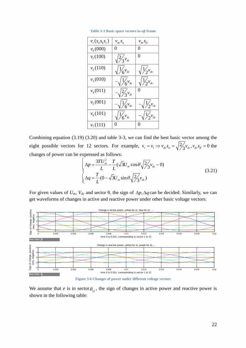
7v (111) 0 0 Combining equation (3.19) (3.20) and table 3-3, we can find the best basic vector among the
eight possible vectors for 12 sectors. For example, 12 , 03r dc dc dcv v v s v v sa b= ⇒ = = the
changes of power can be expressed as follows:
23 2( 3 cos 0)3
2(0 3 sin )3
mm dc
m dc
TU Tp U vL L
Tq U vL
θ
θ
∆ = − −∆ = −
(3.21)
For given values of Um, Vdc and sector θ, the sign of ,p q∆ ∆ can be decided. Similarly, we can get waveforms of changes in active and reactive power under other basic voltage vectors:
Figure 3-6 Changes of power under different voltage vectors
We assume that e is in sector12θ , the sign of changes in active power and reactive power is
shown in the following table:
0 0.002 0.004 0.006 0.008 0.01 0.012 0.014 0.016 0.018 0.02
0
1
2
3
4
time 0 to 0.02s, corresponding to sector 1 to 12
Sig
n of
cha
nge,
pos
itive
zer
o, n
egat
ive
Change in active power, yellow for v1, blue for v2, ...
0 0.002 0.004 0.006 0.008 0.01 0.012 0.014 0.016 0.018 0.02-4
-2
0
2
4
time 0 to 0.02s, corresponding to sector 1 to 12
Sig
n of
cha
nge,
pos
itive
zero
, neg
ativ
e
Change in reactive power, yellow for v1, purple for v2,...

23
Table 3-4 Sign of changes in power
p∆ q∆ 0p∆ > 0p∆ < 0q∆ > 0q∆ = 0q∆ <
0,3,4,5,7v 1v 1,2,3v 0,7v 4,5,6v When 1, 0p qS S= = , it means ,ref refp p q q< > , the voltage vector which can increase active power and decrease reactive power at the same time ( 0p∆ > 0q∆ < ) will be selected, and that is 4 5v and v . When e is in other sectors, and for other combinations of ,p qS S , the same analysis can be made:
Table 3-5 Sign of changes in power in other sectors
1θ 2θ 3θ 4θ 5θ 6θ 7θ 8θ 9θ 10θ 11θ 12θ
0p∆
> 0,7,3
,4,5 0,7,4,5,6
0,7,4,5,6
0,7,1,5,6
0,7,1,5,6
0,7,1,2,6
0,7,1,2,6
0,7,1,2,3
0,7,1,2,3
0,7,2,3,4
0,7,2,3,4
0,7,3,4,5
0p∆
< 1 2 2 3 3 4 4 5 5 6 6 1
0q∆
> 2,3,4 2,3,4 3,4,5 3,4,5 4,5,6 4,5,6 1,5,6 1,5,6 1,2,6 1,2,6 1,2,3 1,2,3
0q∆
< 1,5,6 1,5,6 1,2,6 1,2,6 1,2,3 1,2,3 2,3,4 2,3,4 3,4,5 3,4,5 4,5,6 4,5,6
Then we got the proposed switching table shown in table 3-6.
Table 3-6 Further improved switching table
pS qS , ,a b cS S S
1θ 2θ 3θ 4θ 5θ 6θ 7θ 8θ 9θ 10θ 11θ 12θ 1 0 001 001 101 101 100 100 110 110 010 010 011 011 1 1 011 011 001 001 101 101 100 100 110 110 010 010 0 0 100 100 110 110 010 010 011 011 001 001 101 101 0 1 110 110 010 010 011 011 001 001 101 101 100 100
Comparing the above two tables, we can also find the flaw of this table that the active power is not regulated timely when 0pS = . In each sector, there is only one voltage vector which can be chosen to decrease the active power. This flaw exists in the three switching tables: classical table, improved table and further improved table. It is important to calculate the quotient
23 3m dcU v to determine the change in active power p∆ , as we can see form equation
(3.21), there is a shift in the sinusoidal waveform of p∆ .
5. PI regulator. When losses of R and switches are neglected, the system operates in steady state with unity power factor, we got
24
2
dc dcdc
L
dv vp cvdt R
= + (3.22)
Set 0dc dc dcv v v= + ∆ , the above equation can be written as
0 ( )dc dcdc
L
dv vp cvdt R c
≈ + (3.23)
With Laplace transforms, we got
0( )( ) 1
L
dc dc
L
Rv s vp s R cs
=+
(3.24)
Due to high switching frequency of power inner loop, the power inner loop can be regarded as a small inertia link,
1( )1p
p
G sT s
=+
(3.25)
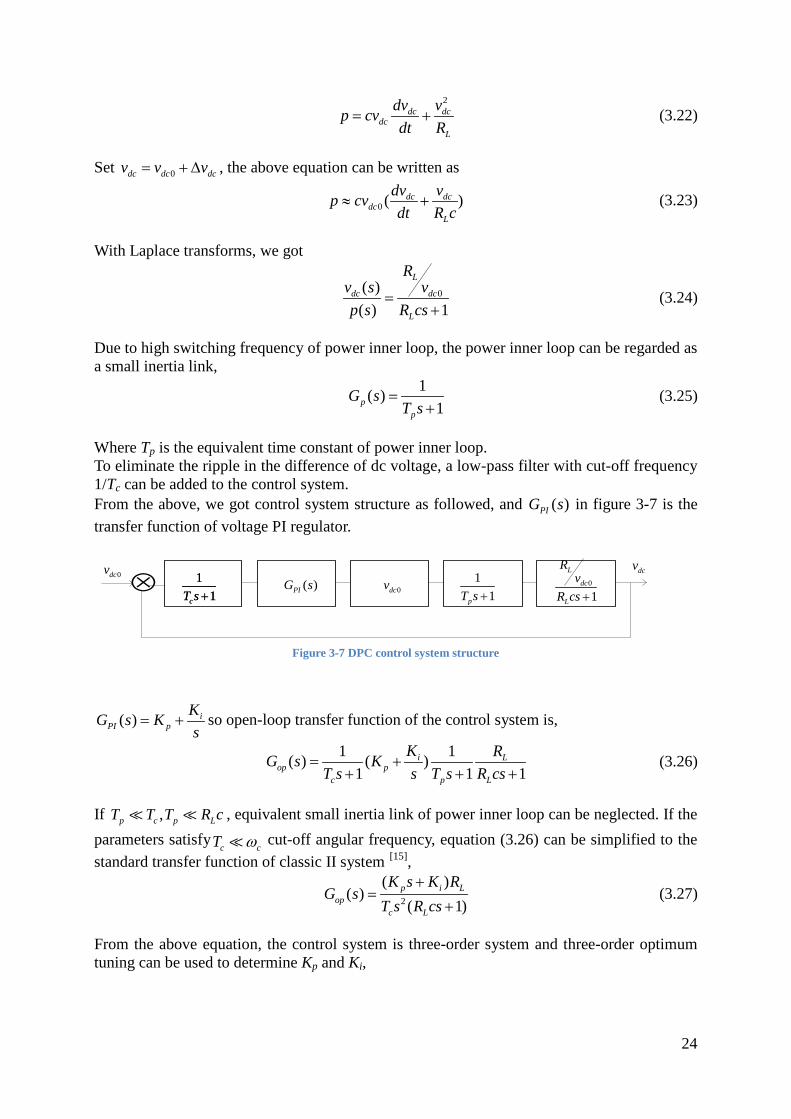
Where Tp is the equivalent time constant of power inner loop. To eliminate the ripple in the difference of dc voltage, a low-pass filter with cut-off frequency 1/Tc can be added to the control system. From the above, we got control system structure as followed, and ( )PIG s in figure 3-7 is the transfer function of voltage PI regulator.
11cT s +
11cT s +
11pT s +
0
1
L
dc
L
Rv
R cs +0dcv( )PIG sdcv
0dcv⊗
Figure 3-7 DPC control system structure
( ) iPI p
KG s Ks
= + so open-loop transfer function of the control system is,
1 1( ) ( )1 1 1
i Lop p
c p L
K RG s KT s s T s R cs
= ++ + +
(3.26)
If ,p c p LT T T R c , equivalent small inertia link of power inner loop can be neglected. If the parameters satisfy
c cT ω cut-off angular frequency, equation (3.26) can be simplified to the standard transfer function of classic II system [15],
2
( )( )
( 1)p i L
opc L
K s K RG s
T s R cs+
=+
(3.27)
From the above equation, the control system is three-order system and three-order optimum tuning can be used to determine Kp and Ki,
25
2
3 2
0.6
0.12
cp
L
ci
L
TKR c
TKR c
= =
(3.28)
3.3 Power flow in the converter Started with mathematical model of PWM rectifier in the two-phase stationary coordinate frame, the power flow in the converter is studied.
dc
dc
diL e Ri v sdtdi
L e Ri v sdt
aa a a
bb b b
= − − = − −
(3.29)
Both ends of the equations are multiplied by ib and ia respectively, and we got,
dc
dc
diL i e i Ri i v s idtdi
L i e i Ri i v s idt
ab a b a b a b
ba b a b a b a
= − − = − −
(3.30)
Subtracting the two equations gives
( ) ( ) ( )dc dc
didiL i i v s i v s i e i e idt dt
bab a b a a b b a a b− = − − − (3.31)
According to the definition of instantaneous power, introduce the concept of instantaneous active and reactive power of AC side of the rectifier.
r dc dc
r dc dc
p v s i v s iq v s i v s i
a a b b
b a a b
= + = −
(3.32)
Disregarding the filter resistance, the energy in the AC-side inductor flows in a form of reactive power. Define the active and reactive power of AC-side inductor:
0i
i
didip L i L idt dt
di diq L i L idt dt
baa b
b aa b
= + =
= −
(3.33)
,didiL L
dt dtba are projection values of the resultant vector of three-phase voltages across the
AC-side inductors along the αβ axes respectively. The equation (3.31) can be expressed as follows: i rq q q= − (3.34)
The above equation shows that the AC-side reactive power of the PWM rectifier is determined by the instantaneous power of inductor and the reactive power that the grid supplies. The instantaneous reactive power of AC inductor is not only in connection with the
26
reactive current, but also active current, which reflects the coupling between the active power and reactive power, and this coupled relationship exists in the form of the inductor power. In particular, when the PWM rectifier operates at unity power factor, sum of AC-side reactive power of rectifier and the reactive power of inductor is zero. Then where does the AC-side reactive power of rectifier go? Both ends of the equation (3.29) are multiplied by ia and ib respectively, and we got,
dc
dc
diL i e i Ri i v s idtdi
L i e i Ri i v s idt
aa a a a a a a
bb b b b b b b
= − − = − −
(3.35)
Adding the two equations gives
2 2( ) ( ) ( )dc dc
didiL i L i e i e i R i i v s i v s idt dt
baa b a a b b a b a a b b+ = + − + − + (3.36)
The above equation can be written in the form of the instantaneous power: i R r0 p p p p= = − − (3.37)
Where Rp means active power consumed by the resistor R. The equation (3.37) clearly shows that the AC-side active power flows from the grid to the AC-side of rectifier. Now analyze the DC-side power flow.
Both ends of the equation ( )dcL
dvC i s i s idt a a b b= + − are multiplied by vdc ,and we got,
( )dcdc dc L dc
dvC v i s i s v i vdt a a b b= + − (3.38)
The left side of the equation is the instantaneous energy of the capacitor C, and the right part can be written as follows: dc dc L dc r Lv s i v s i i v p pa a b b+ − = − (3.39)
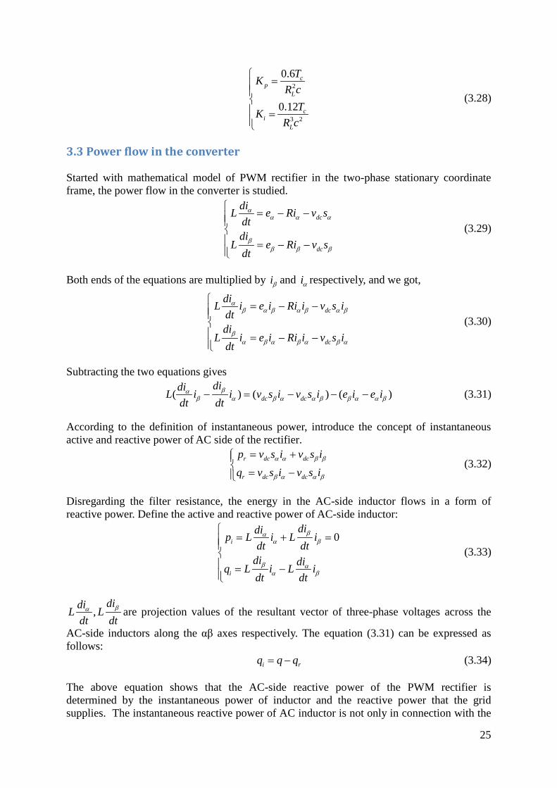
The equation (3.38) can be written in the form of the instantaneous power: C r Lp p p= − (3.40)
Where Lp and Cp are instantaneous load energy and DC capacitor energy respectively. The equation (3.40) shows that the AC-side active power of the rectifier is equal to the load energy plus the capacitor energy and active power goes to the DC side from the AC side of the rectifier. Then we can answer the last question. The AC-side reactive power of rectifier charges the DC-side capacitor to boost the DC voltage. Now we can get the power flow diagram from equations (3.34), (3.37) and (3.40).

27
Rect
ifier
p rp
RpCp
rpLp
AC side
q Cq
DC side
rq
iq
rq
Figure 3-8 Power flow in rectifier
28
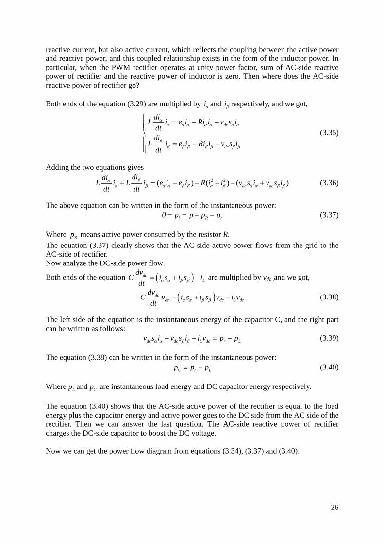
Chapter 4 Principle of Model predictive control Model predictive control strategy has become an advanced process control technology in chemical process industry, and its usage is spreading to other application areas. Model predictive control uses the model to compute a trajectory of a future manipulated variable u to optimize the future behavior of the plant output x (controlled variable). MPC uses the model and the current measurements of the process to calculate the future actions of manipulated variables and ensures the controlled variables and manipulated variables to satisfy the constraints, and then MPC controller puts the first element of the calculated manipulated variable sequences to the process plant.
Figure 4-1 MPC scheme
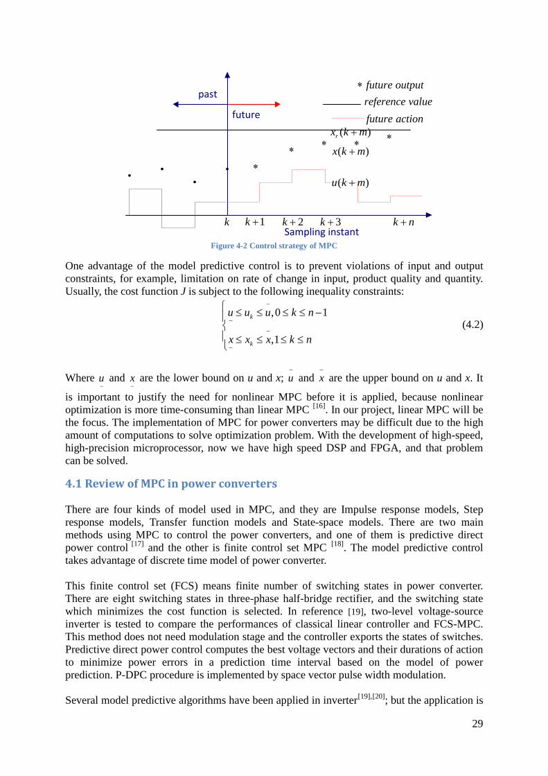
The detailed control strategy is shown in figure 4-2. x is the controlled variable and u is manipulated variable. At the time instant k, with initial state xk, the manipulated variables, at the next n sampling instants, u(k), u(k+1), …, u(k+n-1) are computed. n means prediction horizon. These manipulated variables are calculated to minimize a cost function J, for example, the predicted deviations from the reference trajectory over the next n sampling instants. The first element u(k) will be applied to the system for interval from k to k+1. At the next sampling instant, k+1, the above steps are repeated. Typically, quadratic programming is used to calculate the manipulated variables at each sampling instant.
(4.1)
Where Q and R are weighting matrices used to weight prediction error and control actions. If Q and R are positive definite, the quadratic problem would be convex.
29
future
kSampling instant
( )u k m+
past
1k + 2k + 3k + k n+
∗∗ ∗ ∗ ∗
( )x k m+
∗ future output
future actionreference value
( )rx k m+
Figure 4-2 Control strategy of MPC
One advantage of the model predictive control is to prevent violations of input and output constraints, for example, limitation on rate of change in input, product quality and quantity. Usually, the cost function J is subject to the following inequality constraints:
,0 1
,1
k
k
u u u k n
x x x k n
−
−
−
−
≤ ≤ ≤ ≤ − ≤ ≤ ≤ ≤
(4.2)
Where u−
and x−
are the lower bound on u and x; u−
and x−
are the upper bound on u and x. It
is important to justify the need for nonlinear MPC before it is applied, because nonlinear optimization is more time-consuming than linear MPC [16]. In our project, linear MPC will be the focus. The implementation of MPC for power converters may be difficult due to the high amount of computations to solve optimization problem. With the development of high-speed, high-precision microprocessor, now we have high speed DSP and FPGA, and that problem can be solved.
4.1 Review of MPC in power converters There are four kinds of model used in MPC, and they are Impulse response models, Step response models, Transfer function models and State-space models. There are two main methods using MPC to control the power converters, and one of them is predictive direct power control [17] and the other is finite control set MPC [18]. The model predictive control takes advantage of discrete time model of power converter. This finite control set (FCS) means finite number of switching states in power converter. There are eight switching states in three-phase half-bridge rectifier, and the switching state which minimizes the cost function is selected. In reference [19], two-level voltage-source inverter is tested to compare the performances of classical linear controller and FCS-MPC. This method does not need modulation stage and the controller exports the states of switches. Predictive direct power control computes the best voltage vectors and their durations of action to minimize power errors in a prediction time interval based on the model of power prediction. P-DPC procedure is implemented by space vector pulse width modulation. Several model predictive algorithms have been applied in inverter[19],[20]; but the application is
30
limited to the control of three-phase rectifier. In this project, our main goal is to investigate the MPC of rectifier using discrete-time state-space model for prediction.
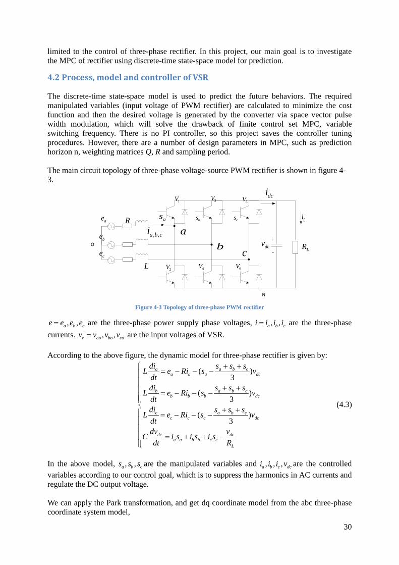
4.2 Process, model and controller of VSR The discrete-time state-space model is used to predict the future behaviors. The required manipulated variables (input voltage of PWM rectifier) are calculated to minimize the cost function and then the desired voltage is generated by the converter via space vector pulse width modulation, which will solve the drawback of finite control set MPC, variable switching frequency. There is no PI controller, so this project saves the controller tuning procedures. However, there are a number of design parameters in MPC, such as prediction horizon n, weighting matrices Q, R and sampling period. The main circuit topology of three-phase voltage-source PWM rectifier is shown in figure 4-3.
ae
be
ce
R
LR, ,a b ci
L
O
b
-dcv
dci
Li
ab c
as
1V 3V5V
2V 4V 6V
csbs
Figure 4-3 Topology of three-phase PWM rectifier
, ,a b ce e e e= are the three-phase power supply phase voltages, , ,a b ci i i i= are the three-phase currents. , ,r ao bo cov v v v= are the input voltages of VSR. According to the above figure, the dynamic model for three-phase rectifier is given by:
( )3
( )3
( )3
a a b ca a a dc
b a b cb b b dc
c a b cc c c dc
dc dca a b b c c
L
di s s sL e Ri s vdtdi s s sL e Ri s vdtdi s s sL e Ri s vdtdv vC i s i s i sdt R
+ + = − − −
+ + = − − − + + = − − −
= + + −
(4.3)
In the above model, , ,a b cs s s are the manipulated variables and , , ,a b c dci i i v are the controlled variables according to our control goal, which is to suppress the harmonics in AC currents and regulate the DC output voltage. We can apply the Park transformation, and get dq coordinate model from the abc three-phase coordinate system model,
31
( )
dd q d dc d
qq d q dc q
dcq q d d L
diL e Li Ri v sdtdi
L e Li Ri v sdtdvC i s i s idt
ω
ω
= + − − = − − −
= + −
(4.4)
Now ,d qs s are the manipulated variables and , ,d q dci i v are the controlled variables. As we can see from the equation, it is a nonlinear system. We use some approximation to simplify the system to get a linear system to apply the linear model predictive control. To achieve the rapid regulation of the DC voltage, ignore the losses on AC side resistor and switches, and we use energy conservation law: input power from the grid should be equal to the load power and capacitor charging power. Assuming that the system is in steady state, and we have dc dcov v= , which is the reference value of output DC voltage. ( )d d q q dco q q d dp e i e i v i s i s= + = + (4.5)
From equation (4.4), we have ,dc dcq q d d L L
L
dv vi s i s C i idt R
+ = + = ,
Substituting for q q d di s i s+ from above equation,
( )dc dcd d q q dco
L
dv vp e i e i v Cdt R
= + = + (4.6)
So we have,
dc d d dc
dco L
dv e i vCdt v R
= − (4.7)
Then the dynamic model of the power rectifier is expressed by:
dd q d dc d
qq d q dc q
dc d d dc
dco L
diL e Li Ri v sdtdi
L e Li Ri v sdtdv e i vCdt v R
ω
ω
= + − − = − − −
= −
(4.8)
Equation (4.8) can be written in a state-space form as follows:
10 0
10 0
0 010
dd
d dc dq q
q dc qdc
ddc
dco L
Ri L Li
e v sRi ie v sL L
vevCv CR
ω
ω
− − = − − + − −
(4.9)
A discrete-time form with sampling time T can be used to predict the future value of

32
controlled variables. Using Euler approximation ( 1) ( )di i k i kdt T
+ −= , we obtain a discrete-time
model,
1 0 0( 1) ( )( 1) 1 0 ( ) 0
( ) 0 0( 1) 0 1
dd
d dc dq q
q dc qdc
ddc
dco L
RT TTi k L Li ke v sRT Ti k T i ke v sL L
v ke T Tv kCv CR
ω
ω
− + − + = − − + − + −
(4.10)
We restate the aim of the model predictive control here, suppressing the harmonics of the input current with unity power factor operation and regulating the DC output voltage quickly, which means 0,q dc dcoi v v= = and id supplying exact required power to the load. So we want our MPC controller to track these references. Then our cost function is,
[ ] [ ] [ ] [ ]1
0
1min ( 1) ( 1) ( 1) ( 1) ( ) ( ) ( ) ( )2
nT T
r r r rk
J x k x k Q x k x k u k u k R u k u k−
=
= + − + + − + + − −∑ (4.11)
Where ( )
( ) ( )( )
d
q
dc
i kx k i k
v k
=
, ( ) d dc d
q dc q
e v su k
e v s−
= − ,
2 0 02 0
0 2 0 ,0 2
0 0 2Q R
= =
.
A quadratic objective function with some linear constraints can be solved by a quadratic program [21]. MPC controller can compute the control action u(k) which minimizes the cost function, and then ( ) ( )dc d dc qv s k and v s k are derived as the desired input voltage to the PWM rectifier. We get the input voltage to the PWM rectifier in dq frame. We have to transform input voltage from dq frame to αβ frame, and then space vector pulse width modulation (SVPWM) is used to modulate this desired space vector:
2 2( ) ( ) ( tan )dc ddc d dc q
dc q
v sV v s v s t arcv s
ω∗ = + ∠ +
4.3 Two-level SVPWM modulation technique
4.3.1 Voltage space vector distribution of three-phase VSR Space vector PWM (SVPWM) control strategy is a novel idea to control the converter. Space vector control strategy was introduced by the Japanese in the early 1980s for AC motor drive system. SVPWM compared to conventional Sinusoidal PWM method has the following advantages: increasing the voltage utilization rate by 15.47%, having a lower switching frequency, easier to implement for microprocessor due to simple vector mode switching. In figure 4-3 and for abc coordinate system, we have

33
( )3
( )3
( )3
a b cao a dc
a b cbo b dc
a b cco c dc
s s sv s v
s s sv s v
s s sv s v
+ += −
+ += −
+ += −
(4.12)
There are six switches and the two switches on the same bridge can not close or open at the same time, so only 23=8 switch combinations exist. The combinations are shown as follows:
Table 4-1 Voltage values of the different switch combinations
Voltage vector switch voltage
as bs cs aov bov cov
0V 0 0 0 0 0 0
1V 1 0 0 23 dcv 1
3 dcv− 13 dcv−
2V 1 1 0 13 dcv 1
3 dcv 23 dcv−
3V 0 1 0 13 dcv− 2
3 dcv 13 dcv−
4V 0 1 1 23 dcv− 1
3 dcv 13 dcv
5V 0 0 1 13 dcv− 1
3 dcv− 23 dcv
6V 1 0 1 13 dcv 2
3 dcv− 13 dcv
7V 1 1 1 0 0 0
It is not difficult to find that the AC side input voltage of different switch combinations can be
expressed by a space vector with length 23 dcv . Take 1V for example, using power invariant
transformation from abc to αβ coordinate system, we got
1 1 212 2 3
22 3 3 1 230 33 2 2 3 01 1 1 1
32 2 2
dc
dc jodc dc
o
dc
vV
V vV v V v e
VVv
aa
b ab
b
− − = = − − ⇒ ⇒ = = −
(4.13)
Number of different switch combinations is limited, so there are only eight basic space vectors 0 1 2 3 4 5 6 7, , , , , , ,V V V V V V V V .
( 1) /3
0,7
2 ( 1,...,6)30
j kk dcV v e k
V
π− = =
= (4.14)

34
4.3.2 Synthesis of voltage space vector
The objective of the SVPWM control is to synthesize the desired AC side input voltage space vector. Six non-zero vectors form six sectorsⅠⅡⅢⅣⅤⅥ. For any given voltage space vector *V , it can be synthesized by the eight basic space vectors, as shown in figure 4-4.
I
II
III
IV
V
VI
1(100)v
2 (110)v3 (010)v
4 (011)v
5 (001)v6 (101)v
7 (111)v
0 (000)v
*V
2 2
S
V TT
1 1
S
V TT
Figure 4-4 basic vectors and sectors
We will focus on the voltage space vector in sectorⅠand later on generalize the discussion to other sectors. 1 2,V V are applied for intervals 1 2,T T respectively, and zero vectors are applied for interval 0,7T to synthesize V ∗ over a time period sT . The voltage vector can be expressed as, *
1 1 2 2 sTV T V V T+ = (4.15)
The angle between V ∗ and 1V is α, according to the sinusoidal law, we got
2 1* 2 1
2 sinsin sin( )3 3
s s
T TV VV T Tπ πa a= =
− (4.16)
And we have dcvVV 32
21 == , the time interval can be calculated as follows:
1
2
0,7 1 2
2sin( )
3
2sin
sdc
sdc
s
VT T
v
VT T
vT T T T
π a
a
∗
∗
= −
= = − −
(4.17)
Constraint of linear SVPWM modulation is, 1 2 sT T T+ ≤ (4.18)
Combining equation (4.17) and (4.18), we got

35
2 2
sin( ) sin3s s s
dc dc
V VT T T
v vπ a a
∗ ∗
− + ≤ (4.19)
The above equation should be tenable for any possible value of α, then we got,
2
dcvV ∗ ≤ (4.20)
If V ∗ rotates at a constant speed in the complex plane, three-phase balanced sinusoidal voltages will be modulated. In fact, V ∗ can only rotates at a stepper speed due to the switching frequency and limited switch combinations. However, the amplitude of the voltage space vector V ∗ should be limited to the circle within the hexagon in Fig.4-4 to prevent
distortion in the AC side currents. It is possible for V ∗ bigger than2
dcv , and this condition
is called over saturation of SVPWM. To solve this problem, let2
dcvV ∗ = .
In practice, there are several ways to synthesize the desired voltage space vectorV ∗ . In this project, seven-segment SVPWM control strategy [22] is used, which reduces the amplitude of harmonic at the switching frequency and improves the waveform quality, however it increases the switching frequency. The seven-segment SVPWM strategy divides the interval 0,7T into three segments, two 0V s lie in the desired vector’s start and end, and 7V lies in the middle ofV ∗ . Two repeated non-zero basic vectors compose two triangles. The order of on and off of six switches should satisfy the following principle: only one of six switches can change the position, close or open, for change of one basic voltage vector to another vector. For example, supposing the voltage vectorV ∗ in sector 1 as shown in figure 4-4. V ∗ is made up of vectors
0 1 2 7 2 1 0, , , , ,V V V V V V and V . The rectifier with this strategy will switch six times in one PWM cycle. For the choice of zero vectors, making fewer changes of switches and reducing the switching losses are the main consideration.
1(100)V
2 (110)V
2 2
2 s
V TT
1 1
2 s
V TT
*V
1 1
2 s
V TT
2 2
2 s
V TT
Figure 4-5 Synthesis of seven-segment SVPWM
Corresponding switch , ,a b cs s s values and switching function waveforms for sectorⅠare shown as follows:

36
Table 4-2 Switch state values
switch 0 1 1 1 1 1 0 0 0 1 1 1 0 0
0 0 0 1 0 0 0
Figure 4-6 Switching function waveforms in sector 1
The flowchart of MPC-SVPWM is drawn below:
Figure 4-7 Flowchart of MPC-SVPWM
For the implementation of SVPWM and MPC controller in Matlab/Simulink, please see the appendix.

37
Chapter 5 Simulation This chapter builds models of DPC and MPC-SVPWM power rectifier in Matlab/simulink environment. Based on these models, their static and dynamic responses, parameter errors on performance and other factors affecting performances are studied and compared. The inductor and capacitor are important components of the rectifier. The AC-side inductor stores energy and filters harmonic currents. It isolates grid voltages from input voltages of VSR and uses the stored energy to boost the DC output voltage. There are two principles for determining value of inductor: meeting the requirement of output power of VSR and good current tracking performance. DC-side capacitor provides a buffer for energy exchange between DC side of VSR and load, and reduces the DC voltage ripple coefficient. There are also two principles for determining value of capacitor: fast voltage tracking capability and good anti-disturbance ability. Combined with engineering practice, trial-and-error method is used to determine the value of the inductor and capacitor.
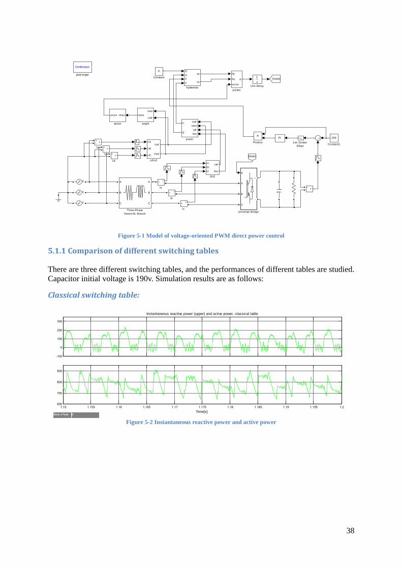
5.1 Simulation of direct power control system Based on figure 3-1 control block diagram and analysis of system composition in 3.2.1 model of voltage-oriented PWM direct power control system is built in Matlab/simulink environment. Figure 5-1 shows the model, and part of the simulation parameters are as follows:
Table 5-1 Simulation parameters
AC side Voltage source peak amplitude 110v Frequency 50Hz Inductance 0.022H Resistance 1Ω
DC side Capacitance 0.0022F Load resistance 50 Ω Given DC voltage 200v
Sampling frequency 20k Hz
38
Figure 5-1 Model of voltage-oriented PWM direct power control
5.1.1 Comparison of different switching tables There are three different switching tables, and the performances of different tables are studied. Capacitor initial voltage is 190v. Simulation results are as follows:
Classical switching table:
Figure 5-2 Instantaneous reactive power and active power
UA
UB
UC
Ualf
Ubet
u3/u2
thetasector
sector
Sp
Sq
sector
g
pulses
Continuous
pow ergui
Ualf
Ubet
Ialf
Ibet
P
Q
power
Q'
Q
P'
P
sp
sq
hysteresis
Ubet
Ualftheta
angle
g
A
B
C
+
-
Universal Bridge
z
1
Unit Delay
v+-
v+-
Uc
v+-
Ub
v+-
Ua
A
B
C
A
B
C
Three-PhaseSeries RL Branch
Product
PI
i+ -
Ic
i+ -
Ib
i+ -
Ia
IA
IB
IC
Ialf
Ibet
I3/I2
[Gate]
[Gate]
200
Constant1
0
Constant
1st-Order Filter
-100
0
100
200
300
Instantaneous reactive power (upper) and active power, classical table
1.15 1.155 1.16 1.165 1.17 1.175 1.18 1.185 1.19 1.195 1.2600
700
800
900
Time[s]
39
Figure 5-3 Instantaneous reactive power and active power, startup
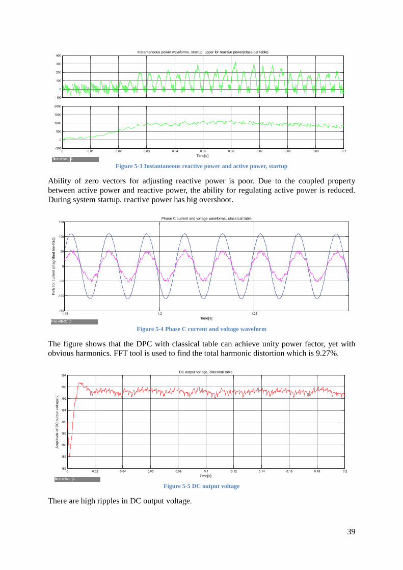
Ability of zero vectors for adjusting reactive power is poor. Due to the coupled property between active power and reactive power, the ability for regulating active power is reduced. During system startup, reactive power has big overshoot.
Figure 5-4 Phase C current and voltage waveform
The figure shows that the DPC with classical table can achieve unity power factor, yet with obvious harmonics. FFT tool is used to find the total harmonic distortion which is 9.27%.
Figure 5-5 DC output voltage
There are high ripples in DC output voltage.
-100
0
100
200
300
400Instantaneous power waveforms, startup, upper for reactive power(classical table)
0 0.01 0.02 0.03 0.04 0.05 0.06 0.07 0.08 0.09 0.1-500
0
500
1000
1500
2000
Time[s]
1.15 1.2 1.25-150
-100
-50
0
50
100
150
Time[s]
Pin
k fo
r cur
rent
(mag
nifie
d te
n-fo
ld)
Phase C current and voltage waveforms, classical table
0 0.02 0.04 0.06 0.08 0.1 0.12 0.14 0.16 0.18 0.2186
187
188
189
190
191
192
193
194
Time[s]
Am
plitu
de o
f DC
out
put v
olta
ge[v
]
DC output voltage, classical table

40
Improve switching table
Figure 5-6 Instantaneous reactive power and active power
Figure 5-7 Instantaneous reactive power and active power, startup
The improved switching table decreases the reactive uncontrollable area. During system startup, active power has big overshoot.
Figure 5-8 Phase C current and voltage waveform
The figure shows that the DPC with improved table can achieve unity power factor with obvious harmonics. FFT tool is used to find the total harmonic distortion which is 7.06%. Harmonics in currents are reduced and the current waveform is improved using this improved
-100
0
100
200
300
Instantaneous reactive power (upper) and active power, improved table
1.15 1.155 1.16 1.165 1.17 1.175 1.18 1.185 1.19 1.195 1.2600
700
800
900
Time[s]
-100
0
100
200
300
400Instantaneous power waveforms, startup, upper for reactive power (improved table)
0 0.005 0.01 0.015 0.02 0.025 0.03 0.035 0.04 0.045 0.05-500
0
500
1000
1500
2000
Time[s]
1.15 1.2 1.25-150
-100
-50
0
50
100
150
Time[s]
Pin
k fo
r cur
rent
(mag
nifie
d te
n-fo
ld)
Phase C current and voltage waveforms, improved table
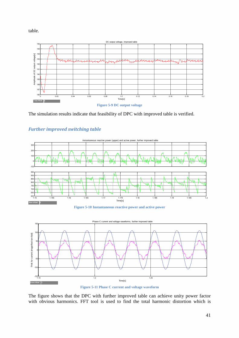
41
table.
Figure 5-9 DC output voltage
The simulation results indicate that feasibility of DPC with improved table is verified.
Further improved switching table
Figure 5-10 Instantaneous reactive power and active power
Figure 5-11 Phase C current and voltage waveform
The figure shows that the DPC with further improved table can achieve unity power factor with obvious harmonics. FFT tool is used to find the total harmonic distortion which is
0 0.02 0.04 0.06 0.08 0.1 0.12 0.14 0.16 0.18 0.2186
187
188
189
190
191
192
193
194
195
196
Time[s]
Am
plitu
de o
f DC
out
put v
olta
ge[v
]
DC output voltage, improved table
-100
0
100
200
300
Instantaneous reactive power (upper) and active power, further improved table
1.15 1.155 1.16 1.165 1.17 1.175 1.18 1.185 1.19 1.195 1.2600
650
700
750
800
850
900
950
Time[s]
1.15 1.2 1.25-150
-100
-50
0
50
100
150
Time[s]
Pin
k fo
r cur
rent
(mag
nifie
d te
n-fo
ld)
Phase C current and voltage waveforms, further improved table
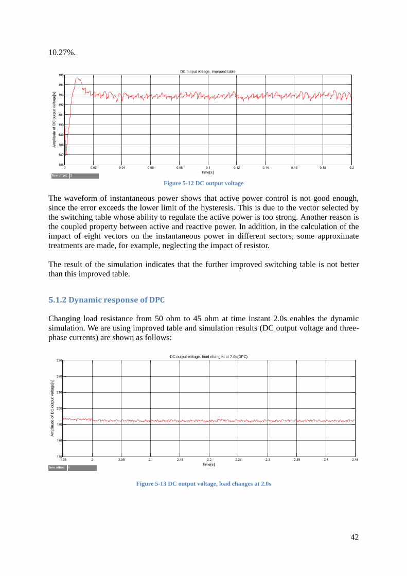
42
10.27%.
Figure 5-12 DC output voltage
The waveform of instantaneous power shows that active power control is not good enough, since the error exceeds the lower limit of the hysteresis. This is due to the vector selected by the switching table whose ability to regulate the active power is too strong. Another reason is the coupled property between active and reactive power. In addition, in the calculation of the impact of eight vectors on the instantaneous power in different sectors, some approximate treatments are made, for example, neglecting the impact of resistor. The result of the simulation indicates that the further improved switching table is not better than this improved table.
5.1.2 Dynamic response of DPC Changing load resistance from 50 ohm to 45 ohm at time instant 2.0s enables the dynamic simulation. We are using improved table and simulation results (DC output voltage and three-phase currents) are shown as follows:
Figure 5-13 DC output voltage, load changes at 2.0s
0 0.02 0.04 0.06 0.08 0.1 0.12 0.14 0.16 0.18 0.2186
187
188
189
190
191
192
193
194
195
Time[s]
Am
plitu
de o
f DC
out
put v
olta
ge[v
]
DC output voltage, improved table
1.95 2 2.05 2.1 2.15 2.2 2.25 2.3 2.35 2.4 2.45170
180
190
200
210
220
230
Time[s]
Am
plitu
de o
f DC
out
put v
olta
ge[v
]
DC output voltage, load changes at 2.0s(DPC)
43
Figure 5-14 Three-phase currents, load changes at 2.0s
Figure 5-15 Phase C voltage and current waveforms, load changes at 2.0s
The following table summarizes the harmonics of current C of steady state before and after load changes:
Table 5-2 THD and value of current C
Ic Peak value(A) Rms value THD Before change 4.714 3.333 7.58% After change 5.198 3.675 6.99%
Magnitude of three-phase currents increased and the DC output voltage barely changed as we decreased the load resistor. The AC-side power is equal to DC-side power. We know that the DC-side power is increased when the load resistance decreases. To increase the AC side power, the AC side currents should increase.
Above simulation results are obtained with a small load change, and test with a big change in load resistance is investigated, load resistance from 50 ohm to 25 ohm at time instant 2.0s. Simulation results are shown as follows:
1.95 2 2.05 2.1 2.15 2.2 2.25 2.3 2.35 2.4 2.45-10
-8
-6
-4
-2
0
2
4
6
8
10
Time[s]
Am
plitu
de o
f cur
rent
[A]
Three-phase current, load changes at 2.0s(DPC)
1.95 2 2.05 2.1 2.15 2.2 2.25 2.3 2.35 2.4 2.45-150
-100
-50
0
50
100
150
Time[s]
Pin
k fo
r cur
rent
(mag
nifie
d te
n-fo
ld)
Phase C voltage and current waveforms, load changes at 2.0s(DPC)

44
Figure 5-16 DC output voltage, load changes to 25 ohm at 2.0s
Figure 5-17 Three-phase currents, load changes to 25 ohm at 2.0s
Figure 5-18 Phase C voltage and current waveforms, load changes to 25 ohm at 2.0s
The following table summarizes the harmonics of current C of steady state before and after load changes:
1.95 2 2.05 2.1 2.15 2.2 2.25 2.3 2.35 2.4 2.45170
180
190
200
210
220
230
Time[s]
Am
plitu
de o
f DC
out
put v
olta
ge[v
]
DC output voltage, load changes to 25 Ohm at 2.0s(DPC)
1.95 2 2.05 2.1 2.15 2.2 2.25 2.3 2.35 2.4 2.45-15
-10
-5
0
5
10
15
Time[s]
Am
plitu
de o
f cur
rent
[A]
Three-phase currents, load changes to 25 Ohm at 2.0s(DPC)
1.95 2 2.05 2.1 2.15 2.2 2.25 2.3 2.35 2.4 2.45-150
-100
-50
0
50
100
150
Time[s]
Pin
k fo
r cur
rent
(mag
nifie
d te
n-fo
ld)
Phase C voltage and current waveform, load changes to 25 Ohm at 2.0s(DPC)
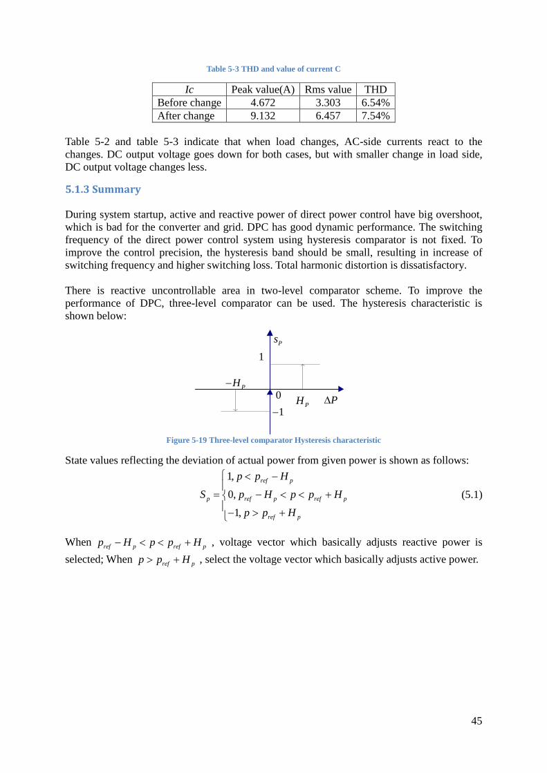
45
Table 5-3 THD and value of current C
Ic Peak value(A) Rms value THD Before change 4.672 3.303 6.54% After change 9.132 6.457 7.54%
Table 5-2 and table 5-3 indicate that when load changes, AC-side currents react to the changes. DC output voltage goes down for both cases, but with smaller change in load side, DC output voltage changes less.
5.1.3 Summary During system startup, active and reactive power of direct power control have big overshoot, which is bad for the converter and grid. DPC has good dynamic performance. The switching frequency of the direct power control system using hysteresis comparator is not fixed. To improve the control precision, the hysteresis band should be small, resulting in increase of switching frequency and higher switching loss. Total harmonic distortion is dissatisfactory. There is reactive uncontrollable area in two-level comparator scheme. To improve the performance of DPC, three-level comparator can be used. The hysteresis characteristic is shown below:
Ps1
P∆0PH−
PH1−
Figure 5-19 Three-level comparator Hysteresis characteristic
State values reflecting the deviation of actual power from given power is shown as follows:
1,
0,
1,
ref p
p ref p ref p
ref p
p p HS p H p p H
p p H
< −
= − < < +− > +
(5.1)
When ref p ref pp H p p H− < < + , voltage vector which basically adjusts reactive power is selected; When ref pp p H> + , select the voltage vector which basically adjusts active power.
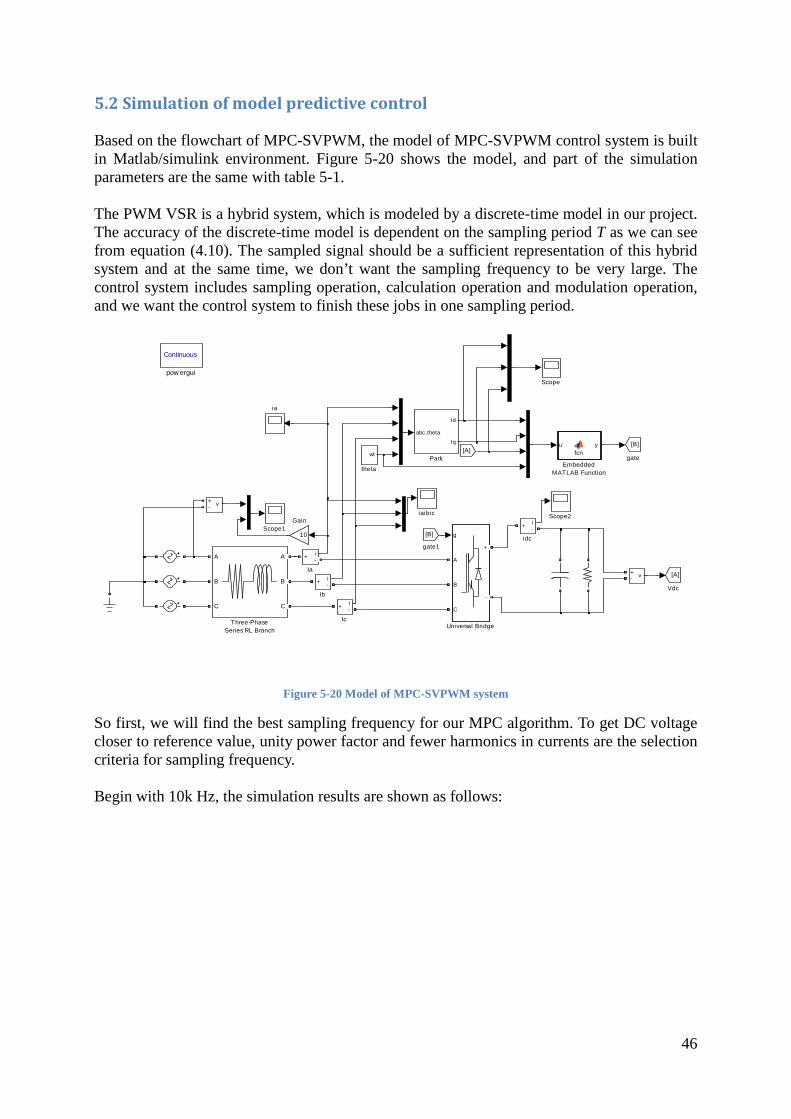
46
5.2 Simulation of model predictive control Based on the flowchart of MPC-SVPWM, the model of MPC-SVPWM control system is built in Matlab/simulink environment. Figure 5-20 shows the model, and part of the simulation parameters are the same with table 5-1. The PWM VSR is a hybrid system, which is modeled by a discrete-time model in our project. The accuracy of the discrete-time model is dependent on the sampling period T as we can see from equation (4.10). The sampled signal should be a sufficient representation of this hybrid system and at the same time, we don’t want the sampling frequency to be very large. The control system includes sampling operation, calculation operation and modulation operation, and we want the control system to finish these jobs in one sampling period.
Figure 5-20 Model of MPC-SVPWM system
So first, we will find the best sampling frequency for our MPC algorithm. To get DC voltage closer to reference value, unity power factor and fewer harmonics in currents are the selection criteria for sampling frequency. Begin with 10k Hz, the simulation results are shown as follows:
wt
theta
Continuous
pow ergui
i+ -
idc
iaibic
ia
[B]
gate1
[B]
gate[A]
[A]
Vdc
g
A
B
C
+
-
Universal Bridge
v+-
v+-
A
B
C
A
B
C
Three-PhaseSeries RL Branch
Scope2
Scope1
Scope
abc,theta
Id
Iq
Park
i+ -
Ic
i+ -
Ib
i+ -
Ia
10
Gain
u yfcn
EmbeddedMATLAB Function
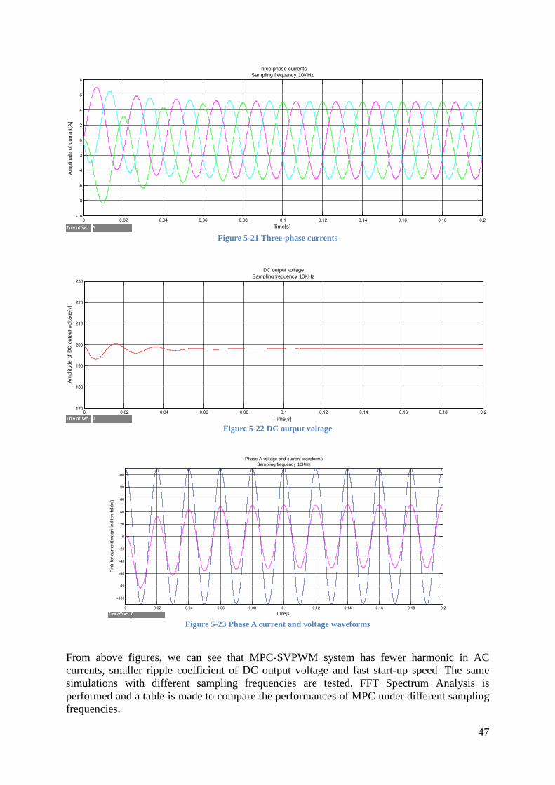
47
Figure 5-21 Three-phase currents
Figure 5-22 DC output voltage
Figure 5-23 Phase A current and voltage waveforms
From above figures, we can see that MPC-SVPWM system has fewer harmonic in AC currents, smaller ripple coefficient of DC output voltage and fast start-up speed. The same simulations with different sampling frequencies are tested. FFT Spectrum Analysis is performed and a table is made to compare the performances of MPC under different sampling frequencies.
0 0.02 0.04 0.06 0.08 0.1 0.12 0.14 0.16 0.18 0.2-10
-8
-6
-4
-2
0
2
4
6
8
Time[s]
Am
plitu
de o
f cur
rent
[A]
Three-phase currentsSampling frequency 10KHz
0 0.02 0.04 0.06 0.08 0.1 0.12 0.14 0.16 0.18 0.2170
180
190
200
210
220
230
Time[s]
Am
plitu
de o
f DC
out
put v
olta
ge[v
]
DC output voltageSampling frequency 10KHz
0 0.02 0.04 0.06 0.08 0.1 0.12 0.14 0.16 0.18 0.2
-100
-80
-60
-40
-20
0
20
40
60
80
100
Time[s]
Pin
k fo
r cur
rent
(mag
nifie
d te
n-fo
lder
)
Phase A voltage and current waveformsSampling frequency 10KHz

48
Table 5-4 DC output voltage and THD under different sampling frequencies
Frequency (Hz) Actual DC output (v) THD in phase current a,b,c 12k 197.0 0.52% 0.51% 0.51% 10k 198.3 0.62% 0.61% 0.61% 8k 199.7 0.76% 0.76% 0.76% 5k 203.3 1.16% 1.16% 1.16%
To solve the following quadratic programming problem is time-consuming.
[ ] [ ] [ ] [ ]1
0min ( 1) ( 1) ( 1) ( 1) ( ) ( ) ( ) ( )
nT T
r r r rk
J x k x k Q x k x k u k u k R u k u k−
=
= + − + + − + + − −∑
For carefully consideration of power factor, DC output voltage, THD in AC currents and calculation in digital control system, the sampling frequency 8 KHz is chosen for our case.
5.2.1 Startup and steady state We can see from equation (4.8) that the MPC model is built based on steady state, which means the capacitor voltage is the reference value 200 v. It is needed to consider whether to pre-charge the DC capacitor in the startup process; it is related to system response speed and transient AC current overshoot problem. It can be predicted that the response speed is slow without pre-charging. In the case of the same simulation model parameters, two situations are simulated: pre-charging DC capacitor and not pre-charging, respectively, and the simulation results are as follows: The capacitor initial voltage is zero:
Figure 5-24 DC output voltage without pre-charging
When the initial voltage across the capacitor is zero, the DC output voltage takes approximate 0.35s to reach the reference value 200v.
0 0.1 0.2 0.3 0.4 0.5 0.60
50
100
150
200
Time[s]
Am
plitu
de o
f DC
out
put v
olta
ge[v
]
DC output voltage without pre-chargingSampling frequency 8KHz

49
Figure 5-25 Grid-side current waveforms without pre-charging
Figure 5-26 Phase A voltage and current waveforms without pre-charging
The capacitor initial voltage is 200v:
Figure 5-27 DC output voltage with pre-charging
0 0.02 0.04 0.06 0.08 0.1 0.12 0.14 0.16 0.18 0.2-25
-20
-15
-10
-5
0
5
10
15
20
25
Time[s]
Am
plitu
de o
f cur
rent
[A]
Three-phase currents without pre-chargingSampling frequency 8KHz
0 0.02 0.04 0.06 0.08 0.1 0.12 0.14 0.16 0.18 0.2-150
-100
-50
0
50
100
150
Time[s]
Pin
k fo
r cur
rent
(mag
nifie
d te
n-fo
ld)
Phase A voltage and current waveforms without pre-chargingSampling frequency 8KHz
0 0.02 0.04 0.06 0.08 0.1 0.12 0.14 0.16 0.18 0.2110
120
130
140
150
160
170
180
190
200
210
Time[s]
Am
plitu
de o
f DC
out
put v
olta
ge[v
]
DC output voltage with capacitor initial voltage 200vSampling frequency 8KHz

50
Figure 5-28 Grid-side current waveforms with pre-charging
Figure 5-29 Phase A voltage and current waveforms with pre-charging
When the capacitor initial voltage is 0, the response speed of DC output voltage and AC-side currents is slow; the grid-side current overshoot is much more serious; the speed of the current tracking voltage phase is slow, taking about a few line cycles. Pre-charging is superior to non-pre-charging. In the following, all the simulations are tested with pre-charging.
5.2.2 Dynamic performance of MPC-SVPWM Performance of MPC depends on the accuracy of the open-loop prediction, which depends on the accuracy of the plant model. Prediction model can not be completely the same with actual plant. Simplification of plant model brings uncertainty. In addition, MPC controller parameters are not same with the main circuit parameters such as resistance, inductance and capacitance. Measurement noise and parameter uncertainty (or variation under operation) degrade the control system performance and even affect system stability. In order to assure the system performances, these factors must be considered in the design of MPC controller, for example, building a system parameter estimator. Some important issues regarding these factors which affect the performance of model predictive control will be discussed in this project.
0 0.02 0.04 0.06 0.08 0.1 0.12 0.14 0.16 0.18 0.2-10
-8
-6
-4
-2
0
2
4
6
8
Time[s]
Am
plitu
de o
f cur
rent
[A]
Three-phase current with capacitor initial voltage 200vSampling frequency 8KHz
0 0.02 0.04 0.06 0.08 0.1 0.12 0.14 0.16 0.18 0.2-150
-100
-50
0
50
100
150
Time[s]
Pin
k fo
r cur
rent
(mag
nifie
d te
n-fo
ld)
Phase A voltage and current waveforms with pre-chargingSampling frequency 8KHz
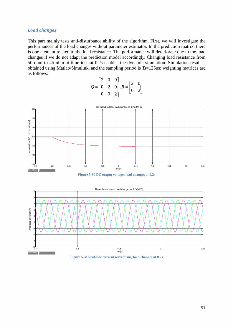
51
Load changes This part mainly tests anti-disturbance ability of the algorithm. First, we will investigate the performances of the load changes without parameter estimator. In the prediction matrix, there is one element related to the load resistance. The performance will deteriorate due to the load changes if we do not adapt the prediction model accordingly. Changing load resistance from 50 ohm to 45 ohm at time instant 0.2s enables the dynamic simulation. Simulation result is obtained using Matlab/Simulink, and the sampling period is Ts=125us; weighting matrices are as follows:
2 0 02 0
0 2 0 ,0 2
0 0 2Q R
= =
Figure 5-30 DC output voltage, load changes at 0.2s
Figure 5-31Grid-side current waveforms, load changes at 0.2s
0.15 0.2 0.25 0.3 0.35 0.4 0.45 0.5 0.55 0.6 0.65170
180
190
200
210
220
230
Time[s]
Am
plitu
de o
f DC
out
put v
olta
ge[v
]
DC output voltage, load changes at 0.2s (MPC)
0.15 0.2 0.25 0.3 0.35-10
-8
-6
-4
-2
0
2
4
6
8
Time[s]
Am
plitu
de o
f cur
rent
[A]
Three-phase currents, load changes at 0.2s(MPC)
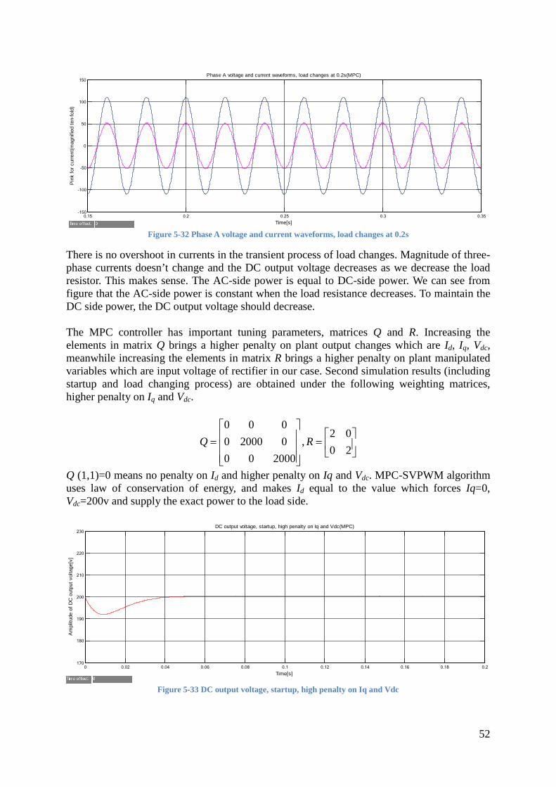
52
Figure 5-32 Phase A voltage and current waveforms, load changes at 0.2s
There is no overshoot in currents in the transient process of load changes. Magnitude of three-phase currents doesn’t change and the DC output voltage decreases as we decrease the load resistor. This makes sense. The AC-side power is equal to DC-side power. We can see from figure that the AC-side power is constant when the load resistance decreases. To maintain the DC side power, the DC output voltage should decrease. The MPC controller has important tuning parameters, matrices Q and R. Increasing the elements in matrix Q brings a higher penalty on plant output changes which are Id, Iq, Vdc, meanwhile increasing the elements in matrix R brings a higher penalty on plant manipulated variables which are input voltage of rectifier in our case. Second simulation results (including startup and load changing process) are obtained under the following weighting matrices, higher penalty on Iq and Vdc.
0 0 02 0
0 2000 0 ,0 2
0 0 2000Q R
= =
Q (1,1)=0 means no penalty on Id and higher penalty on Iq and Vdc. MPC-SVPWM algorithm uses law of conservation of energy, and makes Id equal to the value which forces Iq=0, Vdc=200v and supply the exact power to the load side.
Figure 5-33 DC output voltage, startup, high penalty on Iq and Vdc
0.15 0.2 0.25 0.3 0.35-150
-100
-50
0
50
100
150
Time[s]
Pin
k fo
r cur
rent
(mag
nifie
d te
n-fo
ld)
Phase A voltage and current waveforms, load changes at 0.2s(MPC)
0 0.02 0.04 0.06 0.08 0.1 0.12 0.14 0.16 0.18 0.2170
180
190
200
210
220
230
Time[s]
Am
plitu
de o
f DC
out
put v
olta
ge[v
]
DC output voltage, startup, high penalty on Iq and Vdc(MPC)
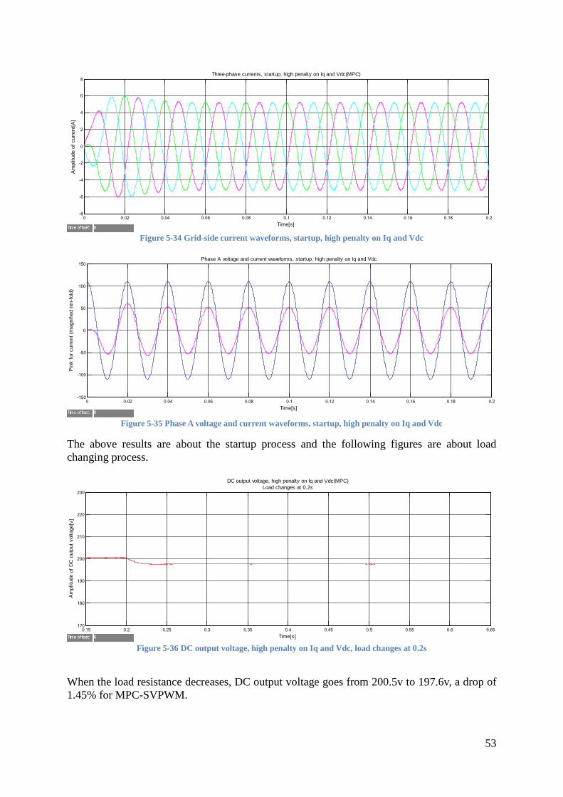
53
Figure 5-34 Grid-side current waveforms, startup, high penalty on Iq and Vdc
Figure 5-35 Phase A voltage and current waveforms, startup, high penalty on Iq and Vdc
The above results are about the startup process and the following figures are about load changing process.
Figure 5-36 DC output voltage, high penalty on Iq and Vdc, load changes at 0.2s
When the load resistance decreases, DC output voltage goes from 200.5v to 197.6v, a drop of 1.45% for MPC-SVPWM.
0 0.02 0.04 0.06 0.08 0.1 0.12 0.14 0.16 0.18 0.2-8
-6
-4
-2
0
2
4
6
8
Time[s]
Am
plitu
de o
f cur
rent
[A]
Three-phase currents, startup, high penalty on Iq and Vdc(MPC)
0 0.02 0.04 0.06 0.08 0.1 0.12 0.14 0.16 0.18 0.2-150
-100
-50
0
50
100
150
Time[s]
Pin
k fo
r cur
rent
(mag
nifie
d te
n-fo
ld)
Phase A voltage and current waveforms, startup, high penalty on Iq and Vdc
0.15 0.2 0.25 0.3 0.35 0.4 0.45 0.5 0.55 0.6 0.65170
180
190
200
210
220
230
Time[s]
Am
plitu
de o
f DC
out
put v
olta
ge[v
]
DC output voltage, high penalty on Iq and Vdc(MPC)Load changes at 0.2s
54
Figure 5-37 Grid-side current waveforms, high penalty on Iq and Vdc, load changes at 0.2s
Figure 5-38 Phase A voltage and current waveforms, high penalty on Iq and Vdc, load changes at 0.2s
The following table summarizes the harmonics of current A of steady state before and after load changes:
Table 5-5 THD and value of current A
Ia Peak value(A) Rms value THD Before change 5.196 3.674 0.75% After change 5.637 3.986 0.69%
When Q = 2*diag([0, 1000, 1000]), R = [2 0; 0 2], higher penalty on Vdc and Iq makes the control more aggressive so that the output tracks the setpoints aggressively and faster. Since a higher value of Q (a lower value of R relatively) gives a smaller punishment on the manipulated variables.
Above simulation results are obtained with a small load change, and test with a big change in load resistance is investigated under the following weighting matrices, load resistance from 50 ohm to 25 ohm at time instant 0.2s. Simulation results are shown as follows:
0.15 0.2 0.25 0.3 0.35 0.4 0.45 0.5 0.55 0.6 0.65-8
-6
-4
-2
0
2
4
6
8
Time[s]
Am
plitu
de o
f cur
rent
[A]
Three-phase currents, startup, high penalty on Iq and Vdc(MPC)Load changes at 0.2s
0.15 0.2 0.25 0.3 0.35-150
-100
-50
0
50
100
150
Time[s]
Pin
k fo
r cur
rent
(mag
nifie
d te
n-fo
ld)
Phase A voltage and current waveforms, high penalty on Iq and Vdc, load changes at 0.2s
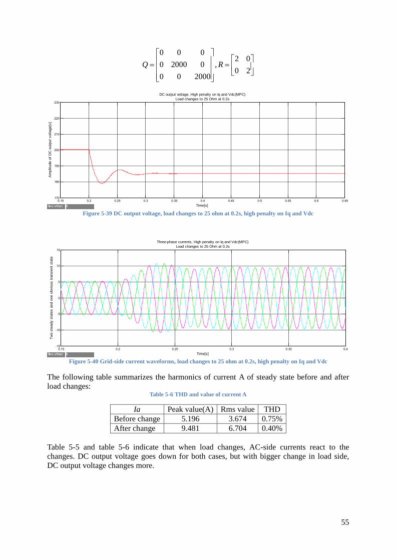
55
0 0 02 0
0 2000 0 ,0 2
0 0 2000Q R
= =
Figure 5-39 DC output voltage, load changes to 25 ohm at 0.2s, high penalty on Iq and Vdc
Figure 5-40 Grid-side current waveforms, load changes to 25 ohm at 0.2s, high penalty on Iq and Vdc
The following table summarizes the harmonics of current A of steady state before and after load changes:
Table 5-6 THD and value of current A
Table 5-5 and table 5-6 indicate that when load changes, AC-side currents react to the changes. DC output voltage goes down for both cases, but with bigger change in load side, DC output voltage changes more.
0.15 0.2 0.25 0.3 0.35 0.4 0.45 0.5 0.55 0.6 0.65170
180
190
200
210
220
230
Time[s]
Am
plitu
de o
f DC
out
put v
olta
ge[v
]
DC output voltage, High penalty on Iq and Vdc(MPC)Load changes to 25 Ohm at 0.2s
0.15 0.2 0.25 0.3 0.35 0.4-15
-10
-5
0
5
10
15
Time[s]
Two
stea
dy s
tate
s an
d on
e ob
viou
s tra
nsie
nt s
tate
Three-phase currents, High penalty on Iq and Vdc(MPC)Load changes to 25 Ohm at 0.2s
Ia Peak value(A) Rms value THD Before change 5.196 3.674 0.75% After change 9.481 6.704 0.40%

56
Figure 5-41 Phase A current and voltage waveforms, load changes to 25 ohm at 0.2s, high penalty on Iq and Vdc
This big change in load causes non-unity power factor.
Parameter error Model Predictive control is a parametric model-based approach and it is sensitive for parameter changes. We have invested the effects of load changes and now we will investigate the filter parameter errors (inductance and resistance) on performances of MPC-SVPWM. The following table summarizes the parameter errors which affects the performances of MPC-SVPWM.
Table 5-7 Parameter errors
Error Filter inductance L AC-side resistance R 0 0.022H 1Ω
-50% 0.011H 0.5Ω +50% 0.033H 1.5Ω
Simulation results are shown as follows:
Figure 5-42 DC output voltage, startup, 0.5L
0.15 0.2 0.25 0.3 0.35 0.4-150
-100
-50
0
50
100
150
Time[s]
Pin
k fo
r cur
rent
(mag
nifie
d te
n-fo
ld)
Phase A current and voltage waveforms, High penalty on Iq and Vdc(MPC)Load changes to 25 Ohm at 0.2s
0 0.05 0.1 0.15 0.2 0.25 0.3 0.35 0.4 0.45 0.5120
130
140
150
160
170
180
190
200
210
Time[s]
Am
plitu
de o
f DC
out
put v
olta
ge[v
]
DC output voltage, parameter error 0.5L
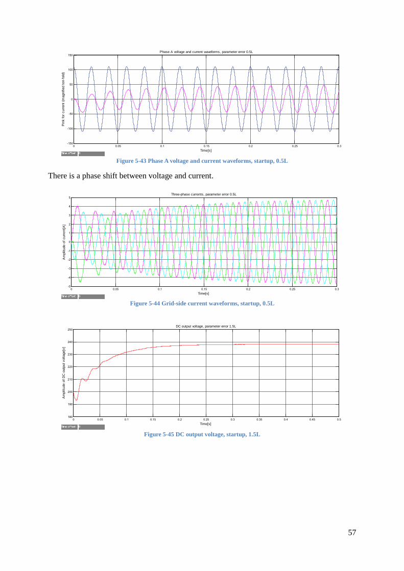
57
Figure 5-43 Phase A voltage and current waveforms, startup, 0.5L
There is a phase shift between voltage and current.
Figure 5-44 Grid-side current waveforms, startup, 0.5L
Figure 5-45 DC output voltage, startup, 1.5L
0 0.05 0.1 0.15 0.2 0.25 0.3-150
-100
-50
0
50
100
150
Time[s]
Pin
k fo
r cur
rent
(mag
nifie
d te
n-fo
ld)
Phase A voltage and current waveforms, parameter error 0.5L
0 0.05 0.1 0.15 0.2 0.25 0.3-5
-4
-3
-2
-1
0
1
2
3
4
5
Time[s]
Am
plitu
de o
f cur
rent
[A]
Three-phase currents, parameter error 0.5L
0 0.05 0.1 0.15 0.2 0.25 0.3 0.35 0.4 0.45 0.5180
190
200
210
220
230
240
250
Time[s]
Am
plitu
de o
f DC
out
put v
olta
ge[v
]
DC output voltage, parameter error 1.5L
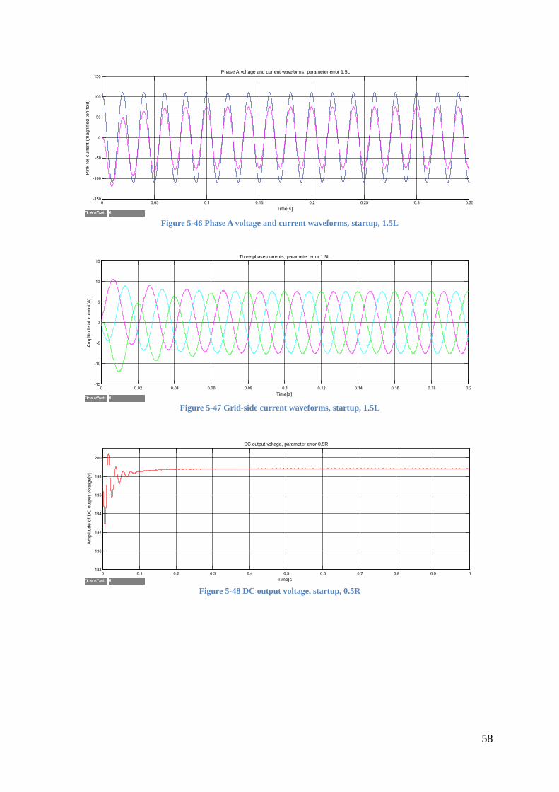
58
Figure 5-46 Phase A voltage and current waveforms, startup, 1.5L
Figure 5-47 Grid-side current waveforms, startup, 1.5L
Figure 5-48 DC output voltage, startup, 0.5R
0 0.05 0.1 0.15 0.2 0.25 0.3 0.35-150
-100
-50
0
50
100
150
Time[s]
Pin
k fo
r cur
rent
(mag
nifie
d te
n-fo
ld)
Phase A voltage and current waveforms, parameter error 1.5L
0 0.02 0.04 0.06 0.08 0.1 0.12 0.14 0.16 0.18 0.2-15
-10
-5
0
5
10
15
Time[s]
Am
plitu
de o
f cur
rent
[A]
Three-phase currents, parameter error 1.5L
0 0.1 0.2 0.3 0.4 0.5 0.6 0.7 0.8 0.9 1188
190
192
194
196
198
200
Time[s]
Am
plitu
de o
f DC
out
put v
olta
ge[v
]
DC output voltage, parameter error 0.5R
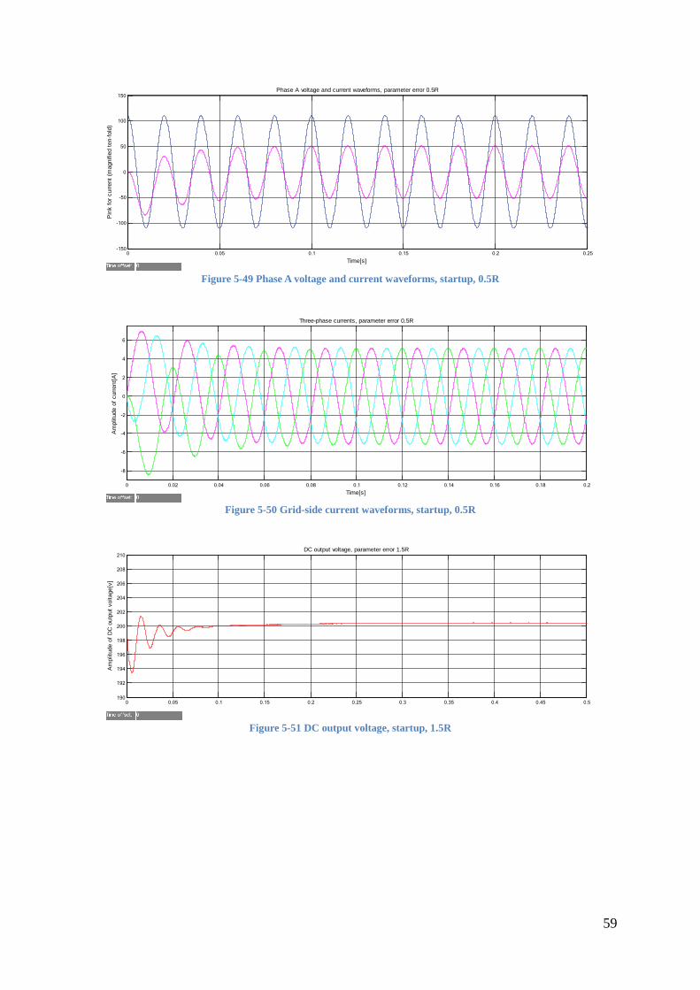
59
Figure 5-49 Phase A voltage and current waveforms, startup, 0.5R
Figure 5-50 Grid-side current waveforms, startup, 0.5R
Figure 5-51 DC output voltage, startup, 1.5R
0 0.05 0.1 0.15 0.2 0.25-150
-100
-50
0
50
100
150
Time[s]
Pin
k fo
r cur
rent
(mag
nifie
d te
n-fo
ld)
Phase A voltage and current waveforms, parameter error 0.5R
0 0.02 0.04 0.06 0.08 0.1 0.12 0.14 0.16 0.18 0.2
-8
-6
-4
-2
0
2
4
6
Time[s]
Am
plitu
de o
f cur
rent
[A]
Three-phase currents, parameter error 0.5R
0 0.05 0.1 0.15 0.2 0.25 0.3 0.35 0.4 0.45 0.5190
192
194
196
198
200
202
204
206
208
210
Am
plitu
de o
f DC
out
put v
olta
ge[v
]
DC output voltage, parameter error 1.5R
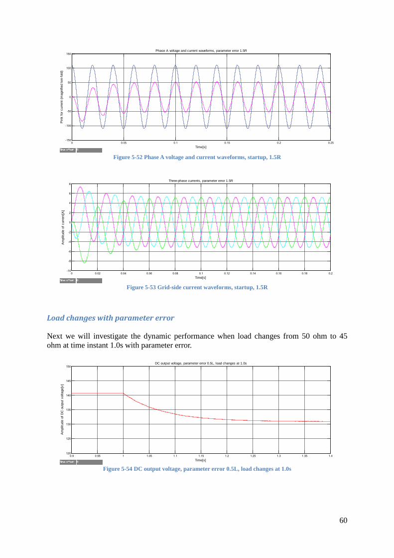
60
Figure 5-52 Phase A voltage and current waveforms, startup, 1.5R
Figure 5-53 Grid-side current waveforms, startup, 1.5R
Load changes with parameter error Next we will investigate the dynamic performance when load changes from 50 ohm to 45 ohm at time instant 1.0s with parameter error.
Figure 5-54 DC output voltage, parameter error 0.5L, load changes at 1.0s
0 0.05 0.1 0.15 0.2 0.25-150
-100
-50
0
50
100
150
Time[s]
Pin
k fo
r cur
rent
(mag
nifie
d te
n-fo
ld)
Phase A voltage and current waveforms, parameter error 1.5R
0 0.02 0.04 0.06 0.08 0.1 0.12 0.14 0.16 0.18 0.2-10
-8
-6
-4
-2
0
2
4
6
8
Time[s]
Am
plitu
de o
f cur
rent
[A]
Three-phase currents, parameter error 1.5R
0.9 0.95 1 1.05 1.1 1.15 1.2 1.25 1.3 1.35 1.4120
125
130
135
140
145
150
Time[s]
Am
plitu
de o
f DC
out
put v
olta
ge[v
]
DC output voltage, parameter error 0.5L, load changes at 1.0s
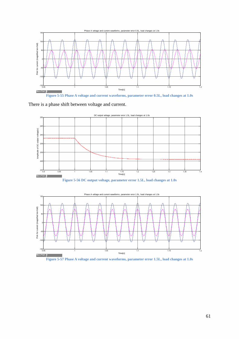
61
Figure 5-55 Phase A voltage and current waveforms, parameter error 0.5L, load changes at 1.0s
There is a phase shift between voltage and current.
Figure 5-56 DC output voltage, parameter error 1.5L, load changes at 1.0s
Figure 5-57 Phase A voltage and current waveforms, parameter error 1.5L, load changes at 1.0s
0.95 1 1.05 1.1 1.15 1.2-150
-100
-50
0
50
100
150
Time[s]
Pin
k fo
r cur
rent
(mag
nifie
d te
n-fo
ld)
Phase A voltage and current waveforms, parameter error 0.5L, load changes at 1.0s
0.9 0.95 1 1.05 1.1 1.15 1.2 1.25 1.3 1.35 1.4220
225
230
235
240
245
250
Time[s]
Am
plitu
de o
f DC
out
put v
olta
ge[v
]
DC output voltage, parameter error 1.5L, load changes at 1.0s
0.95 1 1.05 1.1 1.15 1.2-150
-100
-50
0
50
100
150
Time[s]
Pin
k fo
r cur
rent
(mag
nifie
d te
n-fo
ld)
Phase A voltage and current waveforms, parameter error 1.5L, load changes at 1.0s
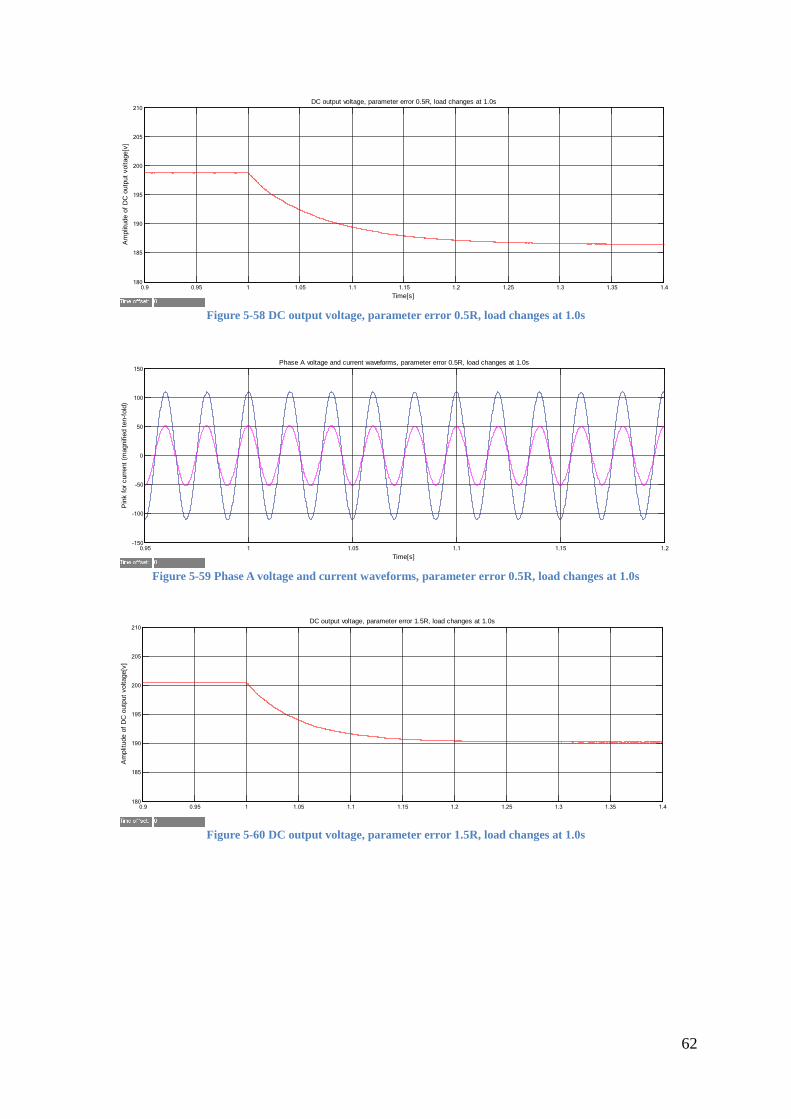
62
Figure 5-58 DC output voltage, parameter error 0.5R, load changes at 1.0s
Figure 5-59 Phase A voltage and current waveforms, parameter error 0.5R, load changes at 1.0s
Figure 5-60 DC output voltage, parameter error 1.5R, load changes at 1.0s
0.9 0.95 1 1.05 1.1 1.15 1.2 1.25 1.3 1.35 1.4180
185
190
195
200
205
210
Time[s]
Am
plitu
de o
f DC
out
put v
olta
ge[v
]
DC output voltage, parameter error 0.5R, load changes at 1.0s
0.95 1 1.05 1.1 1.15 1.2-150
-100
-50
0
50
100
150
Time[s]
Pin
k fo
r cur
rent
(mag
nifie
d te
n-fo
ld)
Phase A voltage and current waveforms, parameter error 0.5R, load changes at 1.0s
0.9 0.95 1 1.05 1.1 1.15 1.2 1.25 1.3 1.35 1.4180
185
190
195
200
205
210
Am
plitu
de o
f DC
out
put v
olta
ge[v
]
DC output voltage, parameter error 1.5R, load changes at 1.0s
63
Figure 5-61 Phase A voltage and current waveforms, parameter error 1.5R, load changes at 1.0s
The following table summarizes the harmonics of current of steady state before and after load changes:
Table 5-8 THD and value of current A
Ia Peak value(A) Rms value THD Figure5-57 Before change 7.545 5.335 0.56%
After change 7.534 5.327 0.55% Figure5-59 Before change 5.138 3.633 0.78%
After change 5.005 3.539 0.77% Figure5-61 Before change 5.207 3.682 0.77%
After change 5.207 3.682 0.73% As we can see from table 5-8, when the load has a small change, the AC-side currents almost don’t change and even become smaller. The system does not work with parameter errors.
5.2.3 Summary The performance is sensitive for parameter changes and parameter errors, especially for the filter inductance. Additional control block with online parameters estimation should be added in order to decrease control sensitivity to parameter changes. Adaptive control can overcome the impact of changes in system parameters and adaptive control applied to the PWM converter is worth studying.
0.95 1 1.05 1.1 1.15 1.2-150
-100
-50
0
50
100
150
Time[s]
Pin
k fo
r cur
rent
(mag
nifie
d te
n-fo
ld)
Phase A voltage and current waveforms, parameter error 1.5R, load changes at 1.0s

64
Chapter 6 Conclusion and future work This thesis carried out the theoretical study and Matlab simulation on the direct power control and model predictive control of PWM rectifier, and completed the following tasks:
• Study the principles of DPC and MPC-SVPWM • Build DPC and MPC-SVPWM models in Matlab/Simulink environment • Compare results from respective models
Through simulation results, conclusions are drawn:
6.1 Conclusions from the Simulink results
1. Sampling rate of MPC-SVPWM scheme is low, reducing the switch loss and increasing its lifecycle. Voltage-orientation direct power control could not achieve the same experimental performance even if the sampling rate is higher.
2. Both MPC-SVPWM and DPC have good dynamic performance when load changes. Model predictive control is a parametric model-based approach and it is sensitive for parameter changes but there is no parameter error issue in direct power control.
3. Synchronous phase angle and frequency are needed for Park transformation in MPC-SVPWM. There is no complicated park transformation in DPC.
Voltage-source PWM rectifier with model predictive control strategy performs better in the following aspects:
• Fewer harmonics in AC currents • Smaller DC voltage ripple coefficient • Unity power factor • Good static and dynamic performance • Higher utilization of the DC bus voltage
The performance of MPC-SVPWM is sensitive for parameters. To increase the performance, the accuracy of a model should be increased, and more exact model should be built. Make less approximate treatment to get the prediction model. Parameter estimator and adaptive control applied to the PWM converter are worth studying to overcome the impact of parameter uncertainty. Though this project achieves its expected purpose, there are a lot of work has to be done, for example, increasing system stability.
6.2 Suggested future work
1. Solving the MPC problem takes a substantial amount of computation time. The computation time should be investigated and compared with the sampling period.
2. Select an appropriate digital signal processor for this demanding power electronics control application.
3. Establish the simulation model in DSP in the lab to verify the algorithm of model predictive control.
4. Energy feedback and the inverter aspects should be included in the experiment. 5. Test other load rather than resistive load in the experiment.
65
Appendix
Deviation of power supply voltages in dq frame ed and eq Three phase balanced power supply voltages are given:
2 cos
2 cos( 2 / 3)
2 cos( 2 / 3)
a m
b m
c m
e U t
e U t
e U t
ω
ω π
ω π
= = −
= +
(1.2)
Power invariant transformation,
cos cos( 2 / 3) cos( 2 / 3)
2 sin sin( 2 / 3) sin( 2 / 3)3
1 1 12 2 2
d a
q b
co
x xx x
xx
θ θ π θ πθ θ π θ π
− + = − − − − +
(1.3)
Note that tθ ω= , therefore,
[ ]
cos 2 cos cos( 2 / 3) 2 cos( 2 / 3)23 cos( 2 / 3) 2 cos( 2 / 3)
cos cos cos( 2 / 3) cos( 2 / 3)2cos( 2 / 3) cos( 2 / 3)3
cos cos cos cos(2 / 3) sin sin(2 / 3)
cos23
m md
m
m
m
U t U te
U t
t tUt
t
U
θ ω θ π ω π
θ π ω π
θ ω θ π ω πθ π ω π
θ ω θ π θ π
⋅ + − ⋅ − +=
+ ⋅ + ⋅ + − ⋅ − +
= + ⋅ + ⋅ + + ⋅
=[ ][ ][ ]
cos(2 / 3) sin sin(2 / 3)
cos cos(2 / 3) sin sin(2 / 3)
cos cos(2 / 3) sin sin(2 / 3)
2 3 3cos cos sin sin2 23
3 cos( )
3
m
m
m
t t
t t
U t t
U t
U
ω π ω π
θ π θ π
ω π ω π
θ ω θ ω
θ ω
+ +
− ⋅ − = +
= −
=
(1.4)
In the same way, we got eq=0.
Switching function waveforms in six sectors
0
4T 0
2T1
2T 0
4T2
2T
1
2T2
2T
as
bs
cs
1
1
1
Figure 0-1 Switching function waveforms in sector 1
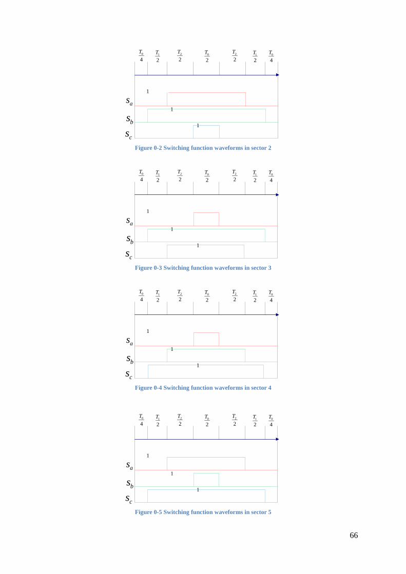
66
0
4T 0
2T1
2T 0
4T2
2T
1
2T2
2T
as
bs
cs
1
1
1
Figure 0-2 Switching function waveforms in sector 2
0
4T 0
2T1
2T 0
4T2
2T
1
2T2
2T
as
bs
cs
1
1
1
Figure 0-3 Switching function waveforms in sector 3
0
4T 0
2T1
2T 0
4T2
2T
1
2T2
2T
as
bs
cs
1
1
1
Figure 0-4 Switching function waveforms in sector 4
0
4T 0
2T1
2T 0
4T2
2T
1
2T2
2T
as
bs
cs
1
1
1
Figure 0-5 Switching function waveforms in sector 5
67
0
4T 0
2T1
2T 0
4T2
2T
1
2T2
2T
as
bs
cs
1
1
1
Figure 0-6 Switching function waveforms in sector 6
Codes in Embedded MATLAB Function % MPC controller function y = fcn(u) % Declare following functions to be extrinsic eml.extrinsic('sparse'); eml.extrinsic('blkdiag'); eml.extrinsic('optimset'); eml.extrinsic('quadprog'); % persistent fcn_caltime; if isempty(fcn_caltime) fcn_caltime = double(zeros(1,1)); end % nu: number of controls persistent nu; if isempty(nu) nu = double(2); end % System matrices Ad and Bd persistent Ad; if isempty(Ad) Ad = double([ 0.9915 0.0393 0; -0.0393 0.9915 0; 0.0383 0 0.9989]); end persistent Bd; if isempty(Bd) Bd = double([ 0.0057 0; 0 0.0057; 0 0]); end % n: Length of control horizon persistent n; if isempty(n) n = double(3); end % Weighting matrix Q and R in cost funtion persistent I_n; if isempty(I_n) I_n = zeros(3);
68
I_n = (eye(3)); end persistent Qk; if isempty(Qk) Qk = double(2*diag([1, 1, 1])); end persistent Rk; if isempty(Rk) Rk = double([2 0; 0 2]); end % Equality constraint persistent Aeq_c1; if isempty(Aeq_c1) Aeq_c1 = zeros(9); Aeq_c1 = (eye(3*3)); end persistent Aeq_c2; if isempty(Aeq_c2) Aeq_c2 = zeros(9); Aeq_c2 = (kron(diag(ones(2,1),-1), -Ad)); end persistent Aeq_c3; if isempty(Aeq_c3) Aeq_c3 = zeros(9,6); Aeq_c3 = kron(I_n, -Bd); end persistent Aeq; if isempty(Aeq) Aeq = zeros(9,15); Aeq = [(Aeq_c1 + Aeq_c2), Aeq_c3]; end % Inequality constraints % Lower bound on x persistent x_lb; if isempty(x_lb) x_lb = double(-Inf(3*3,1)); end % Upper bound on x persistent x_ub; if isempty(x_ub) x_ub = double(Inf(3*3,1)); end % Lower bound on u persistent u_lb; if isempty(u_lb) u_lb = double(-Inf(3*2,1)); end % Upper bound on u persistent u_ub; if isempty(u_ub) u_ub = double(Inf(3*2,1)); end % Lower bound on z persistent lb; if isempty(lb) lb = double([x_lb; u_lb]); end % Upper bound on z persistent ub; if isempty(ub)
69
ub = double([x_ub; u_ub]); end persistent Q_mpc; if isempty(Q_mpc) Q_mpc = double(kron(I_n, Qk)); end persistent R_mpc; if isempty(R_mpc) R_mpc = kron(I_n, Rk); end persistent G_mpc; if isempty(G_mpc) G_mpc = zeros(15); G_mpc = double(blkdiag(Q_mpc, R_mpc)); end persistent Aeq_mpc; if isempty(Aeq_mpc) Aeq_mpc = double([Aeq_c1 + Aeq_c2, Aeq_c3]); end persistent opt; if isempty(opt) opt = optimset('Display','off', 'Diagnostics','off', 'LargeScale','on'); end persistent beq_mpc; if isempty(beq_mpc) beq_mpc = double([zeros(3,1); zeros(2*3,1)]); end % Sampling frequency persistent freq_signal; if isempty(freq_signal) freq_signal = double(8000); end persistent fcn_outstate; if isempty(fcn_outstate) fcn_outstate = double([0,0,0,0]); end persistent fcn_wt; if isempty(fcn_wt) fcn_wt = double(zeros(1)); end persistent fcn_gate; if isempty(fcn_gate) fcn_gate = double(zeros(2,6)); end persistent fcn_limitT; if isempty(fcn_limitT) fcn_limitT = double(zeros(1,6)); end persistent fcn_tnow; if isempty(fcn_tnow) fcn_tnow = double(zeros(1)); end if u(3) <= 0.01 y = [0;1;0;1;0;1]; else % Solve optimization problem at each sampling instant if u(4)/(2*pi*50/freq_signal) >= fcn_caltime x = u(1:3)-[5.938157;0;200]; beq_mpc(1:3) = Ad*x;

70
z = zeros(15,1); %fval = zeros(1); %exitflag = zeros(1); %output = %lambda = struct('lower',zeros(15,1),'upper',zeros(15,1),'eqlin',zeros(9,1),'ineqlin',zeros(0,1)); [z,fval,exitflag,output,lambda] = quadprog(G_mpc,[],[],[],Aeq_mpc,beq_mpc,lb,ub,[],opt); u_mpc = double(z(10:11)); % Only first element is used u_mpc = [125.8147,-41.0416]' - u_mpc; u_mag = sqrt(u_mpc(1)^2 + u_mpc(2)^2); u_angle = acos(u_mpc(1)/u_mag); if u_mpc(2) < 0 u_angle = -u_angle; end u_angle = u(4) + u_angle; if u_mag > u(3)/sqrt(2) u_mag = u(3)/sqrt(2); end while u_angle < 0 u_angle = u_angle + 2*pi; end part_value = u_angle/(pi/3); part_in = fix(part_value); part_angle = u_angle - part_in*pi/3; part_in = rem(part_in,6); part_in = part_in + 1; T_temp = sqrt(2)*u_mag/u(3)*1/freq_signal; T1 = T_temp*sin(pi/3-part_angle); T2 = T_temp*sin(part_angle); T0 = 1/freq_signal - T1 - T2; fcn_outstate = [T1,T2,T0,part_in]; switch (part_in) case 1 fcn_gate = [1,0,0,1,0,1; 1,0,1,0,0,1]; case 2 fcn_gate = [1,0,1,0,0,1; 0,1,1,0,0,1]; case 3 fcn_gate = [0,1,1,0,0,1; 0,1,1,0,1,0]; case 4 fcn_gate = [0,1,1,0,1,0; 0,1,0,1,1,0]; case 5 fcn_gate = [0,1,0,1,1,0; 1,0,0,1,1,0]; otherwise fcn_gate = [1,0,0,1,1,0; 1,0,0,1,0,1]; end % SVPWM modulation fcn_limitT(1) = T0/4; fcn_limitT(2) = fcn_limitT(1) + T1/2; fcn_limitT(3) = fcn_limitT(2) + T2/2; fcn_limitT(4) = fcn_limitT(3) + T0/2; fcn_limitT(5) = fcn_limitT(4) + T2/2; fcn_limitT(6) = fcn_limitT(5) + T1/2; fcn_caltime = fcn_caltime + 1;
71
fcn_tnow = u(4)/(100*pi); end y0 = [0,1,0,1,0,1]; t_now = 0; t_now = u(4)/(100*pi) - fcn_tnow; if t_now < fcn_limitT(1) y0 = [0,1,0,1,0,1]; else if t_now < fcn_limitT(2) y0 = fcn_gate(1,:); else if t_now < fcn_limitT(3) y0 = fcn_gate(2,:); else if t_now < fcn_limitT(4) y0 = [1,0,1,0,1,0]; else if t_now < fcn_limitT(5) y0 = fcn_gate(2,:); else if t_now < fcn_limitT(6) y0 = fcn_gate(1,:); else y0 = [0,1,0,1,0,1]; end end end end end end y = y0'; end end

72
References [1] Sun Zhou; Yin Zhongdong; Chen Anyuan; Zhen Xiaoya; , "Application of voltage PWM rectifier in the charger of electric vehicles based on power feed-forward decoupling control," Electric Utility Deregulation and Restructuring and Power Technologies (DRPT), 2011 4th International Conference on , vol., no., pp.554-557, 6-9 July 2011. [2] Busse Alfred, Holts Joachim, "Multiloop control of a unity power factor fast switching AC to DC converter," Proceeding of Powre Electronics Specialist Conference, 1982, pp.171-179. [3] Akagi, Hirofumi; Kanazawa, Yoshihira; Nabae, Akira, “Instantaneous Reactive Power Compensators Comprising Switching Devices without Energy Storage Components” in Industry Applications, IEEE Transactions on, pp. 625-630. 1984. [4] Green, A.W; Boys, J.T.; Gates, G.F. “3-phase voltage sourced reversible rectifier”, in Electric Power Applications, IEE Proceedings B, Nov 1988, pp. 362 – 370. [5] Dixon, J.W; Boon-Teck Ooi, “Indirect current control of a unity power factor sinusoidal current boost type three-phase rectifier”, Industrial Electronics, IEEE Transactions on, Nov 1988, pp.508-515. [6] Komurcugil, H.; Kukrer, O.; , "Lyapunov-based control for three-phase PWM AC/DC voltage-source converters," Power Electronics, IEEE Transactions on , vol.13, no.5, pp.801-813, Sep 1998. [7] Chenwei, "Research and realization on direct power control of three-phase voltage-source PWM rectifier", Huazhong University of scisece & Technology, 2009. [8] Marei, M.I.; El-Saadany, E.F.; Salama, M.M.A.; , "A novel control scheme for STATCOM using space vector modulation based hysteresis current controller", Harmonics and Quality of Power, 2004. 11th International Conference on , vol., no., pp. 58- 65, 12-15 Sept. 2004. [9] Jain, S.; Agarwal, V.; , "A Single-Stage Grid Connected Inverter Topology for Solar PV Systems With Maximum Power Point Tracking", Power Electronics, IEEE Transactions on , vol.22, no.5, pp.1928-1940, Sept. 2007. [10] Xin-yan Zhang; Xiao-bo Zhang; Wei-qing Wang; Suonan Jiale; , "The Study of on Grid Wind Turbine Generator Made in China", Power and Energy Engineering Conference (APPEEC), 2010 Asia-Pacific , vol., no., pp.1-4, 28-31 March 2010. [11] Ned Mohan, Advanced Electric Drives: Analysis, Control and Modeling Using Simulink, Mnpere, October 2001. [12] Ned Mohan, Tore M. Undeland, William P. Robbins, Power Electronics: Converters, Applications, and Design, Wiley; 3 edition, October 10, 2002. [13] Noguchi, T. ; Tomiki, H. ; Kondo, S. ; Takahashi, I. “Direct power control of PWM converter without power-source voltage sensors” in Industry Applications, IEEE Transactions on, Volume: 34, Issue: 3, pp. 473 – 479, May/Jun 1998. [14] Bouafia, A.; Gaubert, J.-P.; Krim, F, “Analysis and design of new switching table for direct power control of three-phase PWM rectifier”, in EPE-PEMC, pp.703 - 709, Sept. 2008. [15] Brogan,W. “Modern Control Theory”, Prentice-Hall, 1985. [16] Lars Imsland. “Introduction to Model Predictive Control”, May. 2007. [17] YANG Xingwu, JIANG Jianguo, “Predictive Direct Power Control for Three-phase Voltage Source PWM Rectifiers”, Bulletin of Polish Academy of Science, vol. 54, no. 3, pp. 287–292, 2006.

73
[18] Aguilera, R.P. and Quevedo, D.E, “On stability and performance of finite control set MPC for power converters”, Predictive Control of Electrical Drives and Power Electronics, pp. 55-62, Oct. 2011. [19] Larrinaga, S.A.; Vidal, M.A.R.; Oyarbide, E.; Apraiz, J.R.T.; , "Predictive Control Strategy for DC/AC Converters Based on Direct Power Control," Industrial Electronics, IEEE Transactions on , vol.54, no.3, pp.1261-1271, June 2007. [20] Kouro, S.; Cortes, P.; Vargas, R.; Ammann, U.; Rodriguez, J. "Model Predictive Control—A Simple and Powerful Method to Control Power Converters," Industrial Electronics, IEEE Transactions on , vol.56, no.6, pp.1826-1838, June 2009. [21] Jorge Nocedal, Stephen J. Wright, “Numerical Optimization”, pp449, Jul 27, 2006. [22] Shutuan Zhang, Kai Zhang, Zhongshan Jiang and Fang Lu, “Modeling and Simulation of Three-phase Rectifier Based on SVPWM”, 2010 Third International Conference on Information and Computing.