model sp-600-jx - james a. moorer · model sp-600-jx instructions issue 2 - march 1951 manufactured...
TRANSCRIPT

GENERAL PURPOSE
COMMUNICATIONS RECEIVER
MODEL SP-600-JX
INSTRUCTIONS
ISSUE 2 - MARCH 1951
Manufactured by
THE HAMMARLUND MFG. CO. INC.460 West 34th St. New York 1, New York, U.S.A.
GENERAL PURPOSE
COMMUNICATIONS RECEIVER
MODEL SP-600-JX
INSTRUCTIONS
ISSUE 2 - MARCH 1951
Manufactured by
THE HAMMARLUND MFG. CO. INC.
460 West 34th St. New York 1, New York, U.S.A.
Printed in U. S. 1\.

FIG 1FRONT VIEW .SP-600-JX INOFC RECEIVERABINET
2

TABLE OF CONTENTS
Title
T1::chnical Summary
General Description
II Circuit Description
II [ Installation ...
Page
,5
6
8
IV Operation and Description of Controls .........•.....
V Maintenance ....
VI Alignment ..
VII Conversion of Table Model Receiver for Rack Mounting .....
Table I-Tube Socket Voltages.
Table 2-Tube Socket Terminal Resistances.
Table ~-RF and HF Oscillator Alignmcm fro:quencics .........•...•...............
Table 4-Approx. Signal lnputs at IF and AF St;I~CS.•.••.•.•.•••••..•••...•..•.•.
Table 5-Parts List
ILLUSTRATIONS
9
12
16
10
II
13
II
17
Figure
Figure 2
Figure
Figure ,Figure 5
Figure 6
FIgure 7
FIgure 8
Figure 9
Figure 10
Figure II
FIgure 12
Figure I:;
Figure 14
Front View of Receiver SP·600·jX, in cabinet..
Block Diagram
Location of Tubes and Adjustments .
Audio and Overall Fidelity Curves .
Selectivity Curves
Rear Vicw of Receiver .
Top View of Receiver .
Top Vio:w of Receiver-eapaciror Shield Removed ...
BoHom View of Receiver SP·600-JX ...
BoHom View of Receiver-Tuning Unit Shield Removed.
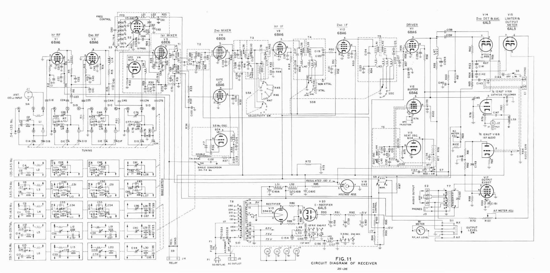
Circuit Diagram of Receivcr. .
Connection Diagram-Recclver Chassis.
ConncctiOn Diagram-Tuning Unit .....
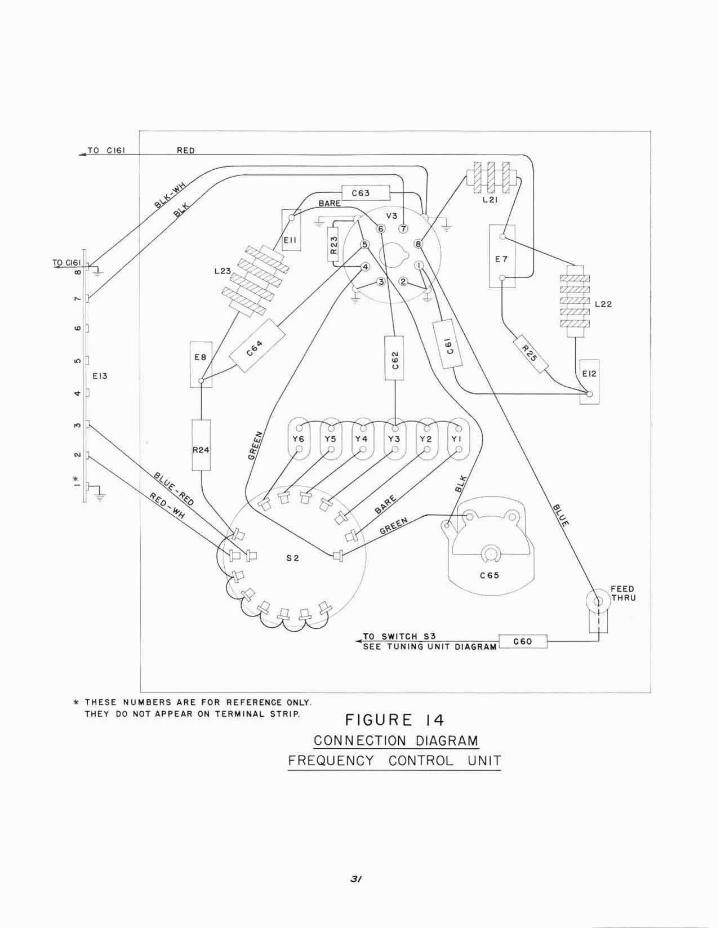
Connection Diagram-Frequency Control Unit.
2
7
I'
14
15
20
21
23
24
25
27
29
JI
3

.54 to 54.0 me
.,54 to 1.3.5 mc1.3.5 to i,45 mci.45 to 7.•0 mc7,40 to 14.8 mc
\•.80 to 29.7 mc29.70 to .504.0 me
7- 68A6.'- 6C.1- 6AC72 - 68E6J- 6ALS1- 12AU71-6V6CT1-5R4CY1- OA2
GENERAL PURPOSE COMMUNICATIONS RECEIVER
MODEL SP-600-JX
TECHNICAL SUMMARY
Electrical CharacteristicsFrequency Range--cotal 6 bands .......•.........•....•....•....•....•....•....•.....
Band I ..........................••......•••••••...••....•......••.•.••.•.....Band 2 .........................•............................. _.......•.......Band .\ ....................•..............•....•....•....•....•....•....•.....Band -4 •.....•.•.........••..•.•.••.•..••.••••••••••••••••••••••.••...•.•..••.Band 5........................... . .Band 6 .............................................•....•...•..••...•....
Maximum UndistorlW Output-approximate-2.5 waUS.
Output Impedance-600 ohms-balanced split windmgs.Phone jack-winding: delivcrs 1.5 milliwatts to iln 8000 ohm resistivc 10ild, when the iludio output to the600 ohm power lood is adjusted to .500 milliwalt5.
Power Supply RequirementsLine Rating _ _. . . . . . . . . . 95, 105, 117, DO, 190, 210, 234 OInd 260 volt tilpS, 50-60 cyeln.Power COIl5\lmpuon.................................. 130 watts. 1.25 ilrnpt. ilt 117 vol1$-mill:irnum.
Tube Complement - total 20RF, fF and BFO A.mplifiers .................•..... _ _ .HF, 2nd ConversIOn and BFO O.scillillors , ....•...••........Crystal Controlled HF Oscillator ....................................•..•.•.. _.•......Mi:ters ..............................................................•.... _ .Detector, "C" Bias Rectifier and Noise Limiter & Meter Rectifier .......•....•............AF Amplifier and IF Output ......................................•... , ...• , .Power Oul put .........................................................•...........Rectifier , ..............................•......Voltage Regulator .
Mechanical SpecificationsRack Modcl- Dimensions: 19 Ulchcs wide, 100 Inches high and 160 inches deep from rack mountingsurface. Weight 66 lbs.Table Modcl- DImensIOns: 21H Inches wide. 12.l.j inches high and 17}i inches deep. Wei~ht 87'~ lbs.
Performance Data - (approximate valurs·takt'h on a sample rect'iver)SenSItivity is 2.3 miuO\'olu, or beuer, throughout the entire frequency n.nge. for a signal to nOIse power ratiooflOto1.Image rejection ratios are better than 80 db throughout the frequency n.nge.The IF rejection ratio at 600 kc is 1700 to 1The AVC action will maintain the output constant within 12 db when the input is increased from 2 to200,000 microvolts.
4
GENERAL PURPOSE COMMUNICATIONS
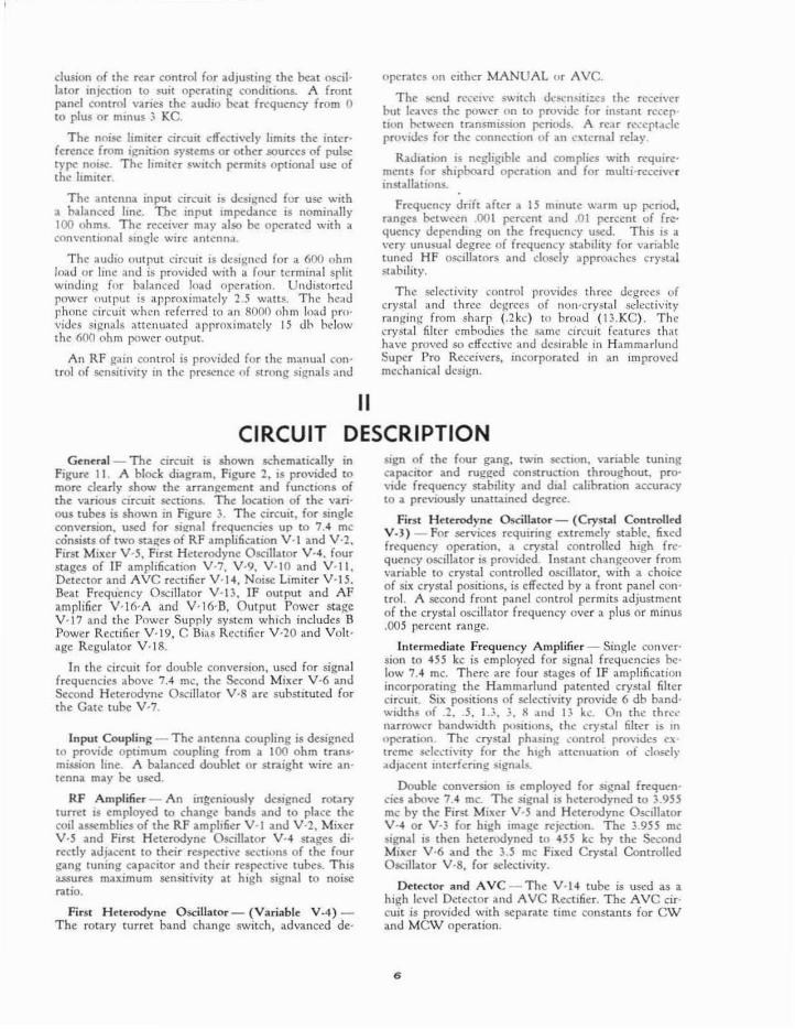
GENERAL DESCRIPTION
RECEIVER
The SP·600-]X is a 20 tube Radio CommunicationsReceiver with self contained power supply. The JXsuffix in this model number denotes that this receiveris made in accordance with JAN specifications. withthe exception of the use of a few capacitors and resis·tors where special design considerations require specialvalues and tolerances nm included in the JAN preferred value lists or where space limitations do notpermit their use. The special componclHs so used arcequal or su~riur to the JAN components in quality.
The receiver is supplied in either a well vcntil:l.tcdsteel, tanle model cabinet finished in dark grey to complement the lighter ~rcy front panel or for mountingin a standard 19 inch rclay rack.
The self contained power supply is designed foropcntion from a single phase. 50 to 60 cycle ahemating current power source. The power transformerprimary is provided with taps covering a line voltagerange from 90 to 270 volts. The power consumptioniF no watts.
The receiver is suitable for either headphone or louospeaker reception of AM radio telephone, CW tcle~raph or AM MCW telegraph signals.
The standard modd provides continuous coverageover a frequency range from 0.54 to 54.0 megacyclesin sill: bands. The lar~e eHily operated band changecontrol knob. on the front p.lncl, selects the desiredfrequency band and a band indicator visible througha small front p.lncl window indicates the frequencyhand 1Il u~e. This control also aligns the dial frequencyindi..:ator with the pr()pcr dial scale.
In addition to the frcqucnc}' scal..:.s, the. main dialhas an arbitrary ~::tle which in conjunction with theband spread dial provides continuous band sprcadscales Over each frequency band f{lr clI:tremely ::tccu'r:\tc logging and resctability.
The single tUlling control is large and of special design to permit ma:<immn traverse speed as well as e:<ccptional opcrating case. It controls both the mainand band spread dials. An anti-backlash gear trainprovides extremely close calibration accuracy and completely accurate resctlbility. A tuning lock providespositi\·e locking action without affecting the frequencysetting.
The tuning ratio from the tuning control to themain dial is 50 to I and the ratio from the band spreaddial to the maiJl dial is 6 to 1.
An ingeniously designed rotary turret is employedto change bands and to place the coil assemblies ofthe RF amplifier. Mixer :lnd First Heterodyne Oscil·
5
lator stages directly adjacent to their respective 5ec'tions of the four gang tuning capacitor and their re'spccti"c tubes. This assures mall:imum sensitivity athigh signal to noise ratio.
Two stages of tuned radio frequenc}' amplificationarc provided on all bands. The circuit for single conversion, uso.:d 011 frequencics up to 7.4 megacycles, includes a mixer, h.:terodync oscillator, fnur stages ofIF amplification, detector and AVC rectifier, noiselimiter and meier rectifier. beat frequcncy oscillator,be;ll frequcn.:y buffer ;lmplifier. IF output, A.F amplifier and output powcr stage. The drcuit for doublecOllversion. employed for frequencies abo\'!': 7.4 mega·cycles, include,; a second m;lI:cr and a second heterodyne crystal controlled oscillator. The power supplysystem includes a B powo'r rectifier, C bias rectifier and,I voltage regulator_
The frequency control unit provides for fixed channel crystal controlled operation on any six frequencieschosen within the range of the ro.:ceivcr. Front panelcomrols permit the sele.:tion of the normal hig:h stability continuously variahle lUning or either of the sixselected fixed fretjuency signals. F(lr crystal controlledfixed channc1l)pcr:Hion it is only nl:ccssary to set thedial to the signal frequency, switch to the crystal frequency desired and tunc with the delt,1 frequency con'trol. Nl) retuning of the main tuning is necessary ordesirable, when swit.ching (rom VFO to crystal opera·tion for the same signal frequency. These crystals arcnot supplied with the rCCclvl:f, but shnuld be purchased on special order from HAMMARLUNDMFG. CO. specifying: the signal frequency for whichIt is til (unction.
The two scale tuning meter 11I1rm.dly lIlclk,ltes therdative strength of the r..:ccived signal in db from 1microvolt, when operatcd on A VC ;\110 with the RFg;lin cOlltrol ;ll maximum. A re,lr .:ontrol is providedfor adjl.1stmcnt at the plus 20 db scale reading with anRF signal input of 10 mi.:rovolts. 011 depression of thepanel meter switch the lower scale of the metcr indicates the audio output power level in db from 6 milli'watts. A rear control is provided for adju.stlOent ofthe 0 db reading.
The AVC circuit is provided with s.:par:ltc timeconstants for CW and Mew (lperatioll. The beat frequency oscillator employs a hIgh cap,lClty Colpitts circuit which gives a high ordcr of frcquency stabilityand minimizes oscill:llOr harmonics. The beat frequency oscillator vollage is introduced into lhe dctcctor through a buffer amplifier which eliminat.esoscillator lock-in. This feature mdkcs it possible totune signals sharply to :cro beat and permits the in-
dusion of the rear control for ;adjustine the beat ascii·lator lIlJecrion to suit opcr.umfZ" .:onditions. A frontfUnd control varies the audio Ix.t frequency from 0to plus or rnmU5 3 KC.
The nni~ limiter circuit effectively hmits the inter·ference from ic:nition systems or other .soUft:es of pulsetype nOI~. The hmitcr SWItch permits optional usc ofthe hmlter.
The antenna input cirCUli is duiJ,.:ned for USl: wuha halanccd Ime. Thc mput Impedancc IS nominally100 ohms. The receiver may also be operated with ;aCOnventional STOgie wire antcnn,l.
The audIO output circULt IS tle~IJ:JH:d for a 600 ohmload (lr Illle and is provided with a four terminal spiltwllldlrl~ for balanced load oper-ttiOIl. Undlstoncdpower output IS approll:imatcly 2.5 W;lttl!. The headphone circuit whell referred to;'1I1 ROOO (111m load provides si~nals ;"tlcnuated apprOll:imatcly 15 dl:- helowthe 600 ohm power output.
An RF f!ain conlrol is provided for the manual COil'trol of sensitlvity In the prescnce of strong signals and
tlper-lles on either MANUAL or Aye.
The scnd rc':CI\'O:: switch dl:5Cn~ltl:es the receiverbut Ic,Ixcs the power on to provide for mstant recep'tlon ~twccn transmissIOn pcmx!s.. A re,lr re.:ept'Il.:leproVides for the connectiun uf an external rela)'
Radiation is negligible :lIld complies with requir~
ments for .!lhlpboard OflCr:lIIOn and for multi·rccclwrinsullations.
Frequency drift after a IS mlllute warm up pcmx).ranges between .001 percent and .01 pcr..:enr of frequency depending on the frequency u$:d. This IS avcry unusual dCj.!fCe of frequency stability for \'an,lbletuned HF oscillators and dosd}' appro.1.chcs crystal.!ltabllity.
The selectivity control pro\'ides three degrecs ofcrystal and three degrees of nOll'cryst:11 .selectivityranging from sh;'trp (.2kc) tl) broad (13.KC). Thecrystal tiltcr embodies the S,IIllC Circuit fealures thathave provcd so effective OInd deSIrable ill HammarlundSuper Pro Recei\'.::rs. incorporated in an improvcdmechanical design.
IICIRCUIT DESCRIPTION
Gtntral- The circuit is shown schem;atie:tlly inFigure 11. A block diagram. Figure 2. is provided tomore deilfly show [he arranflemen[ and functions ofthe various Circuit sections. The locatlon of the van'ous tubes is shown in Figure J. The circuit, for singleconversion. used for sienal frequencies up [0 7.4 meconsists of two staJtes of RF amplification V·I and Y·2.First MotU Y,S. First Heterodyne Oscillator Y-4. fourstagCll of IF amplification Y'?, Y·9. Y·IO and Y-li,Detector and Aye rectifier Y·H. Noise Limiter Y·15.Beat Frequency Oscillator Y-n. IF output :md AFamplifier Y·16·A and Y-16-B. OutpUt Power st'ageY'J? and the Power Supply system which includes BPower Rectifier Y-19, e Bias Rectifier Y·20 and Yoh·age Regulator V-JB.
In the circuit for double convcrsion. used fnr signalfrequencies above 7.4 me. the Second Mixer Y'6 andSecond Heterodyne Oscillalor Y·S are substituted forthe Gate tube Y-?
Input Coupling - The antenna coupling is designedto provide optimum coupling from ;a 100 ohm trans'miMion Ime. A M.laneed doublet or straight wire an'tenna may be used.
RF Amplifiu - An ingeniously designed rotarylurret is employed to change bands and to place theCOli as-~mblies of the RF amplifier Y·I and Y·l, MixerY·5 and First Heterodyne Oscillator V·4 stages di·rectly adjacent to their respeetiv~ SC.:tl(1115 of the fourgang tuning capacitor and their respective tubes. ThiSassures maximum sensitivity at high signal to noiseratio.
Firsf Heterodyne O.scil1ator_ (Variable V4)The rotary turret band change swilch, advanced de·
Sign of the four gang, twm section. \'anable tunlllgcapacitor and rug~ed construction throughout. pro'Vide frequency stability and dial calibration accuracyto a previously unattained degree.
First Heterodyne Oscillator - (Crystal ControllrdV.j) _ For services requmng extremely stable. fixedfrequency operation. a crystal controlled high fre·queney oscillator is proVided. Instant ch"n~eover fromvariable to crystal controlled oscillator. with a choiceof silt crystal positions. is effected by a front panel con'trol. A .second front panel control permits adjustmentof the crystal oscillator frequency over a plus Of minus.005 percent range.
Intermediale Frequency Amplifier - Single cOllver'sion to 4S5 kc is employed for signal frequencies be'low 7.4 mc. There arc four stages of IF ampltficationincorporating the Hammarlund patented crystal filtercircuit. Six positions of scl~etivlty prOVIde 6 db band·widths of 2•.5, 1.3. :.. Sand 13 kc. On the thre.:narrower bandwidth positions, th.: cry9.,,1 filta IS III
IIpcratlQl\ The .::rystal ph<lsmg .:ontrol prOVides extreme SCIC':I1\·lty for tho? high :lttenualloo of dC1SClr,tdJ.cent lllierfermg sign:lls.
Double conversion is employed for signal fre.quen'des alXl\"c 7.4 me. The signal IS heterodyned to :;.955me by the First Mixer V·S and Heterodyne Oscllla!OrY'4 or Y'3 for high Image rejection. The 395S mesignal is then heterodyned to 455 ke by the SecondMixer Y'6 and the 3.05 me Fixed Crystal ControlledOscillator Y·B, for selectivity.
Detector and AVC - The Y,14 tube is used as ahigh levcl Detector and Aye RectIfier. The Aye cir·euit is provided with separate time constants for CWand Mew operation.
6
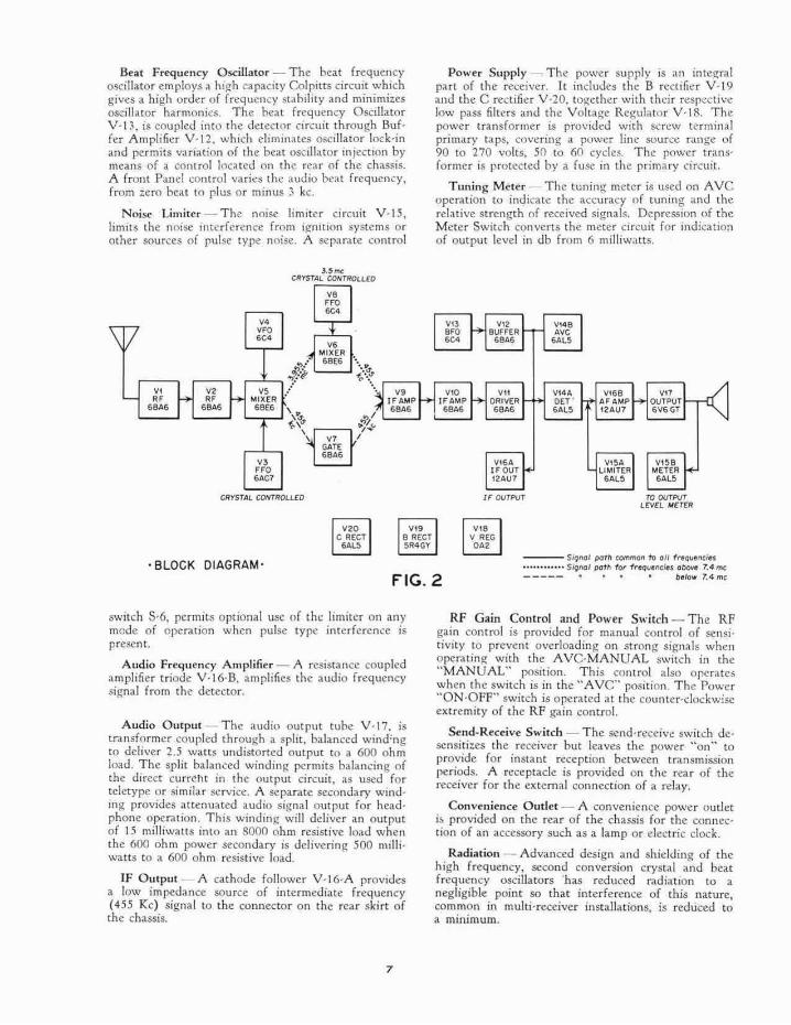
Beat Frequency Oscillator - The beat frequencyoscillalor employs a high capacity Colpitts circuit whichgives a high order of frequency stabIlity and minimiz.esoscillator harmonics. The beat frequency OscillatorY-I 3. is coupled into the detector circuit through Buf·fer Amplifier Y-12. which eliminates oscillator lock-inand permits vuiation of the beat oscillator injection bymeans of a eOlllrol [l1cated on the rear of the ch;lssis.A frolll Panel control varies the audio beat frequency,from "era beat to plus or minus 3 kc.
Noise Limiter-The noise limiter circuit Y-15,limits the noisc interference from ignition systems orOther sources of pulse type noise. A separate control
,,~
Clll'$TAl CONrllOllEO
Power Supply - The power supply is an imegralpart of the recei ...'er. It includes the B recnfit'r Y'19and the C rectifier Y-20, together with their respectivelow pass filters and the Yoltage Regulator Y·IS. Thepower transformer is provided with screw terminalprimary taps, covering a power line source range of90 to '270 volts, 50 to 60 cycles. The power transformer is protected by a fuse in the primary circuit.
Tuning MelCr- The tuning meter is used on AYCoperation to indicate thc accuracy of tuning and therelative strength of received signals. DeprcS5ion of theMeter Switch converts the meter circuit for indicationof output level ill db from 6 milliwatts.
IF outpur
''0c REcr
""",a RECT
5R4GY '"II REG0"
,BLOCK DIAGRAM'f1G.2
---Sl9nQI II'lT~ e,,"'"wm ft> "" f"Q~ne;n............ 5'9"'" pot!> fGI' frfll~1ICj•• obG';. 7.4""• • b.'o... 7.4 me
switch S-6, permits optional use of the limiter on an)'mode of operation when pulse type interference ispresent.
Audio Frequency Amplifier - A resistance coupledamplifier triode Y·16-B. amplifies thc audio frequencysignal from the detector.
Audio OUfpul-The audio output tube Y·17. istransformer coupled through a split. balanccd wind:ngto deliver 2.5 watts undislOrted output to a 600 ohmload. The split balanced winding pcrmilS balancing ofthe direct currellt in the Output circuit, as used forteletype or similar service. A separate secondary wllld·ing provides attenuated audio signal output for headphone operation. This winding will deliver an outputof 15 milliwatts inro an 8000 ohm resistive load whenthe 600 ohm power secondary is delivering 500 milli·watts to a 600 ohm resistive load.
IF Outpul- A cathode follower Y-16·A providesa low impedance source of intermediate frequency(455 Kc) signal to the connector on the rear skirt ofthe chassis.
7
RF Gain Control and Power Switch - The RFgain control is provided for manual control of sensi·ti\.ity to prevent overloading on strong signals whenopcratin2 with the AYC·MANUA.L switch in the"MANUAL" position. This comrol al.so operateswhen the switch is in the" AVC" position. The Power··ON-OFF" switch is operated at the counter-clockwiseextremity of the RF gain control.
Send·Receive S..... itch - The send-receive switch dc·scnsitizes the receiver but leaves the power "on" toprovide for instant reception between transmissionperiods. A rl!ceptacle is provided on the rear of thereceiver for the extental connection of a relay.
Convenience Outlel - A cOllvenience pOwcr outleti1> provided on the rcar of the chassis for the connec'tion of an :lccessory such as a lamp or electric clock.
Radiation - Advanced design and shielding of thehigh frequency, second conversion crystal and beatfrequency oscillators 'has reduced radia'tioll to anegligible point so that interference of this nature,common in multi· receiver installations, is reduced toa minimum.
IIIINSTALLATION
Tu~s and Packing-Inspect the chusis to see thatall tubes are: firmly in their respective sockets ;md tha.tany p;lcking is removed from the receIver.
Power Supply- Make sure that the primary taplead on the power tri!.l1sforrner is connected to thetransformer tap which most nearly agrees with the 50to 60 cycle power source voltage.
Anlenna - The input impedance at the antennaterminals is designed to match OJ. 100 ohm transmissionhne. The angle plug adapter and connector. suppliedWIth the receiver, is designed for use with a small diameter, "TWINAX" tr.tnsmission Ime, which shouldbe used with a bab.nced antenna Installation. If it isdeSired to operate with a smgle wi~ antenna. the ;mleona lud·in wire should be. connected to one tcrminOlIof the connector plug and a ground lead should beconnected from the other terminal of the connector
plug to the ground terminal. whIch is adjacent to the;l.ntenna input receptacle :u the reu of the tumng unit.
Speaker - The loud spea kcr should be of the pt:rmanent magnet dynamic typt: and should include aspeaker voice coil to 600 ohm linc matching traIl!former for connectiOn to the 600 ohm audio outputterminals of the receiver.
Headphones - Either low or hi~h impedance head·phones may be used in the phone jack. The high 1m·pedance type is recommended. The phone jack IS 10CilIOO at the lower left side of the front panel.
Mounting - The receivcr may be plotced on a tahleor mounted In a ~D.ndard 19 lOch nll'k. If a table modelIS purchased. It is supplied WIth a steel cablllel Thecabinet should be placed in a position which permlUthe free access of air for the ventilation louvers.
IVOPERATION
DESCRIPTION OF CONTROLSThe front panel dials and controls ue shown in
Figure I and the rear chassis skirt controls ilnd terminals are shown 10 FIgure 6.
Tuning Dials - The milin diiil is to the left and theband spread dial is to the right. The main dial has sixfrequency band scales, calibrated in megat:yclcs and anarbItrary, outer scale. The band spread dial has an arbItrary. 0 to 100. scale The numernl under the fixedp,.,inter of the main dial indicates the number of revo'lutions thilt have been made by the band spread dialat any setting Thus. if the pointer, for the outerscale. of the main dial indicates over the figure 4 andthe bitnd spread dIal indicates 87.6. the reading to lol,!lor this setting IS read. 487.6. This precise mechanicalhand spread system divides the rotation of the maindIal over each frequency band into approximately 600band spread divisions. with one half division calibra.tlOn pomts. SlOce it is easy to estimate one tenth dIVislons. on the I»nd spread snle, thLS divides each frequency hand into itpproximately 6000 readilble settings. ThIS permits extreme i1ccuracy in the logging ofstations.
Crystal Controlled HF Oscilla.tor - for operntionon fil(eJ frequency chilnncls the "FREQUENCYCONTROL" IS provided. The crystals are not supplied with the receiver, hut will be supplied on specialorder. In order to insure correct crystal controlledfrequency operation crystal units should be orderedfrom HAMMARLUND MFG. CO. INC. and theorder should specify the signal frequency. for whicheach unit is to be used. The frequency control unithas provision for six crystals. Variable frequency op-
cration or crystal controlled frequcncy operation onany of the six crystOlI positions is sclected by the"CRYSTAL SWITCH". The crystal OSCillator is desIgned for uSC! WIth suitOlble crystals at ;)Iny frequency10 the rnnge of the receiver Olbo".:: one megacycle. The"DELTA FREQ" control is uSC!d to compcns..lte for avery small plus or minus frequency tolerance of thecrystals.
The procedure for crystal frequency control operation should be as follows: Loosen the knurled thumbscrew on top of the crystal unit and push the retainerspring assembly to the reu. lnscn the crystal or cry'stals in the crystal sockets, numbered I to 6. Bring thel'Ctainer spring assembly fOl"\ollard so th;n the sprinc:spress on top of the cryst41 holders and tl.ghten thethumb screw. Mark the sign:lll frequency for whicheach crystal was selected. in megacycles on the plasticchart provided for this purposc alongSIde the crystalswitch. PenCil or mk may be used and can be ernsedIf It is desired to change these figures at any time. Thenumerals on the chart should be used !O that theyagree with the numerals on the crystal socket positions.which are also indicated by the crystal switch. Themain tuning dIal should be set at the signal frequencyfor which oocration IS desired. The crystal switchshould be set at the pOsition corresponding to thenumber for that si~nal frequency on the chart. TheDelta Frequency control should be adjusted for m:tximum si~nal or for 2.ero beat as required. It ~hould benOled that this luning adjustment of the Delta Frequency control must be made each time that the si~
nal frequency is changed and that the main tuning dIalshould be set to agree with the new signal frequency.
"
Tuning Lock - The tumng lock, located to theright of the tumn~ knob, ptovidcs a posillVC lockingfor the tuning me.:hamsm without affecting the fre'quency settmg. when it IS clesLrt~d tl) prevent accidentalshlflln~ of the tumO(:: or when the receiver is operatedunder:" severe condition of 'I.-ibration.
Tuning Meter- The tunmg metcr at the upperleft on the front pand 15 useful m a..::curau:ly tunm~ asljtnal and provides ;m mdic.ition of the relativcstrength of the rccel'l.'ed signal in clb from I microvolt.The "METER AD) RF" ,:ontml at the rear of thechassis proVides adjustment of the plus 20 db readmRon the Rf scale, with a 10 microvolt input signal. Dc,pression of the "METER SWITCH" co",,'ercs themeur circuit for Illdlcatl0n of the AF output powerI~vcl in t1b from 6 mllhwaltS. This switch is springreturned to the RF scale cirCUlt pnsition when releasedand should 110t be depressed for Ihe AF scale ulIlcssthe audio output has bC1'1i adjuslcd for 10", po",cr outpili, by means of hcadphones or speaker. Failure toobserve this precaution may re<ult ill dama~e 10 themeter. The "METER AD) AF" control at the rear ofthe chassis proVides adjustment of the 0 db reading (Inthe AF scale. which should be made when the AF out·put power from the 600 ohm ,lUdio output termllldls IS
6 milliwatts or 1.9 voll.5 acrOM :l 600 ohm load
Band Change - Th~ large knob, to the left. is theband change 1.'0ntroi. Each revolution of thiS controlturns the turret. contilimn,l:l the RF and HF oscil1uorCOIl, tnmmer and SWlt.:h cont<lct <tsscmbiic.s, from onefrequency band to the neX[. The turret has no stopsand m<lY ble turned 11\ either direction desired. A po.!Iitive detent machanism <lSsures correct location of thevarious bands. The: band change control simultaneously operates the small frequency band dial, locatedat the center of the panel and aligns the dial frcquenC)findIcator with the proper scale.
Selectivity Switch - The selectivity switch providesthree crystal and three non-crystal degrees of sclel.'tlvity. ranging from extremely sharp, for CW recep'tlOn. LO broad for good fidelity MCW opc.r,luon. Thecontrol knob di;ll indicates the 6 db band width at eachsetting.
Phasing Control - The phasing control permitshlllh attenuation of closely adjacent channel interference on either side of the signal frequency. when thecrystal selectivity positions are used.
Beat Frequency Oscillator - The: 1>£at frequencyos..:lll,ltor is turned "on" for CW si~na.1 operuinn bytht: "MOD-CW" SWitch. The heat frequency dial
l>hould be set at z.ero for tunin~ to l.ero beat and thenadJum:d to -,!,i"e the desired audio pitch. The heat frequency OSI:llIator inJection '·olu.gc is ;p.dJostablc hy the"BFO IN)" control on the rt:;1r skirt of the chassis_
No~ Limiur - The noise limiter switch i lOdepend..nt of other controls a.nd is useful 10 e:rca.t1y attl'nua.ung nolSC mterference from ignluon or similarpulse .ype sources. regardless of the mode of operation.
Send-Recdve - The send· receive switch permitsdescnsitl:ing the receiver during transmission periods.to prevent damage to the receiver. when operated inproximity to the lransmitter ;\nd provides instant re~
turn to reception between transmission periods
Relay Receptacle - The relay receptacle. on therear of the receiver. is connected in paralh::l wHh thel>cnd-rcceive switch ;\nd provides for the connl;ctiorr ofan externally connected relay. to perform the scnd·receive operation. When the relay is used the send·receive switch is left in the "open" or "scnd" position.
A VC-Manual Switch - The AVC-Manual Switchpi'rmlts the chOice of either AVC or Manual sensillvIty Oper.ttlOIi as desired. The AVe has a dcldy bias.which insures maximum sensitivity for weak Signals.
RF Gain Control- The RF gain contrlll prOVidesadjustment of the sensitivity for signals of varioussuength. when under the "manua'" opcratlllg condition. in ordi:T th.u the receiver scnsitivit)· may be adJusted to SUit the Signal strength and prevent owrloadmg_ This control IS also in the cirCUli when Opeutllll::on AVe. III order that the senSitivity may be adJu5h:::dto reduce undCSll'<Ible nOISC dunng "off" periods III thetransmission of the received si~nal. When it IS dc'Sired to use the tunin~ meter fllr indication of rc!atn·csignal strength. the RF gain control should be at maxImum.
Audio Gain Control- The audio galll control adJUSts the audiO input to the audio >tmpldier tube. Itshould be adjusted for the reqUIred audio output whenoperating on AVe and is nest left :n or ncar maximumwhell operating 011 MANUAL contro!'
Phono Input - Termmals arc provided on the rearof the n;cclver for phonograph or other audl() freoquency source IIlput to the audiO frequency a.mplifier.
Convenience OUllet - A pow.::r outlet receptacle isprovided on the rear of the receiver chassis for operatmg an accessory, !Uch as an dectne dock or lamp.
V
MAINTENANCEThis receiver IS deSigned for continuous duty and
should normally require httle attention beyond thereplacement of tubes. However, should trouble develop that c-a.nnot be eliminated with new tubes, thesocket voltages and resistances should be measured to.:hassis. Any ;\PPTf'l.'iable departure from the valuesshown in tables 1 and 2 will generally indicate the
9
L-omponent or circuit at fault.
Opcratinf[ and maintenance of the rccel'l.·er will be~reatly facilitatecl if the contenlS of this instructionm;\nual are thoroughly dit;ested. Approximate lIlputsignal values for stajZe hy !ta.$tc gain checks arc shownIII table 4.
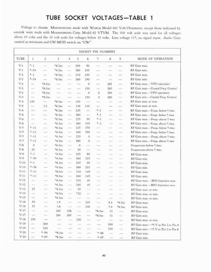
TUBE SOCKET VOLTAGES-TABLE 1
Volu,gc to chusis. Ma.surements m.de with Westen Model 661 Volt-Ohmmwer. except those indIcated by
<Istcflo!k were milde with Mca.surcrncnu Corp. Model 62 VTVM. The 500 ..-olt scale "''as used for all "'oltagcs
above 10 volts iilld the 10 volt scale (or voluges below 10 volts. Lme \'Oltagc 117, no signill mpu!. Audlu G:am,,:oolrol at minimum and C\V-MOD SWitch on "CW"
SOCKET PIN NUMBERS
TUBE I 2 , • , • , , , MODE OF OPERATION
V·I '-I - -6.3ac - '00 '0 - - - RF G:lIn max.
V·I ·-5~ - ·6.3:1.<:- - 260 III - - - RFG~m min.V., '-I - -6.1;0., - 210 100 - - - RFCam mn.
V·, ·-5-1 - ·6.33C - '60 1<0 - - - RF Gain min.
V., - ·6.h.c - - - 0 - 265 - Rt' G;o.m max.-VFO operatlon
V·, - t6.hc - - - ISO - 2" - RF Gam mn.-Crystal fretl. ControlV., - t6.h.c - - - 0 0 290 - RF O,lIn mm._VI'Q operation
V., - -6.h.c - - - ISO 0 280 - RF Gam mm.-Cr~·5tal Frcq. ContrQ[
V·. 130 - -6.);&c - 130 - - - - RF Gam mn. or mm.V·, - l.l t6.3ac - 1<0 110 - - - RF Gam max. or mm.
V.• - - -6.hc - ns - '-I - - RF Gam mu.-Frc'ls. bc-Iow 1.4mc
V·. - - '6.lac - '60 - '-I - - RF Glom m,n._Frc'l" b<low 7 4mcV., - - '6.lac - 225 90 '-I - - RF G:un mn. FrclI,.loixwc 7.4mcV•• - - '6 hc - '60 10' '-1 - - RF Gaon mm. Frrq$.lobovr 7.-4mcV., '-II - -6hc - 225 170 - - - RF Gam mu.-Frrq,. brlow 1 4mc
V·, '-II - '6 lac - 260 190 - - - RF Glom mon.-frrqs.. b<low 1 4mc
V·, '-II - '6hc - 215 0 - - - RF Gam mu -Frtqf. abovc 7..4mcV., '-II - '6.3at - 260 0 - - - RF Gloon mm.-Frrq5...bolle 7.4mcV., 0 - '6 lac - 0 - - - - FrrquenclCf below 7.4mc
V·, '0 - '6.3:.c - '0 - - - - freqUtnen:f lobovt 7.-4mt
V·, '-I - '6.lae - 205 '0 - - - RF Glom mu.V., '-54 - '6.3:.c - 260 235 - - - Rf Glom mm.V·IO '-1 - '6.3:.r - 105 '0 - - - RF Gain mon.
V·IO '-54 - '6.3ae - 260 235 - - - RI'Cain min.V·II --II - '6.3:.c - 210 '<5 - - - RF C;lln max.
V·II '-II _. '6lar - 240 1<5 - - - RI' Cain min.
v·n - - '6.lae 210 .0 - - - RF C:l1n max nro h1ltetion maxv·n - - '6.3loC 140 <5 - RF Gam nun,-BfO Inll:CllOn max.V·13 " - e6 hc - " - - - RF C.un mu. "r nunV'14 - - '6.hc - '22 - - - - RF Gloin max. or mm.V·iS - - ·6.hc - - - - - - RF Glom lOU. or m,n.V-16 '0 - Il - - HO - ••• '6.3lo( RFCa,n mu.V'16 52 - I' - ~ '<0 - ,.. '6.3..( RF Cain min.V-11 - - 260 228 - - '6 he 12 - RF Glom muV-17 ~ - 280 2" ~ - '6.3u 13 - RF Gam mm.Y·18 "0 - - - "0 - - - - RF Gain ron or min.Y-19 - '00 - - - - - '00 - RF Gain mu-'S Y I( Pon 2 to Pm IIV-19 - no - - - - - 520 ~ RF Gam mm.-'S V loe Pin 2 [0 Pm 8V-lO - '-96 '6.lae - - - '-96 - - RFGlom mn.V-20 - '-97 '6.31oc - - - '-97 - - RFGalll min.
10
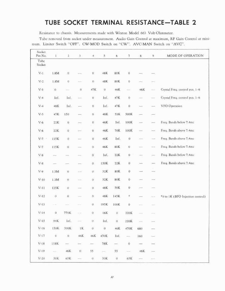
TUBE SOCKET TERMINAL RESISTANCE-TABLE 2Resistance to chassis. MC,l.Surcmcnts made wIth WestOll Modd 663 Volt-Ohmmeter,
Tub.:. removed from socket under Illcasurcm..:m. Audio Gain Control ,n maximum, RF Gain Control at mini"
mum. Limiter S\\!ltch "OfF". CW·MOD Switch on "CW", AVe·MAN SWitch all ..AVe",
SocketPin No. , , 8 , MODE OF OPERATION
Tub.::Socket
V., 1.8M 0 0 -18K SOK 0
V·l L.8M 0 0 <8K 80K 0
V·3 0 0 47K 0 <16K 'oK Crystal Frc,,!_ ,<mtrol pu~. ,-,V·, Inr. Inf. 0 In£' 47K 0 Cr}'sl;Il frc",. control pus. ,-,V·, '8K I "f. 0 luI. <1K 0 vre Operatlon
V·5 47K 150 0 <8K 51K SOOK
V·, nK 0 0 46K Info ,OOK !'rel.!. Band~ below 7 -Ime
V., nK 0 0 -16K 70K LOOK I'rcq. Bands above 7.4me
V., IISK 0 0 <OK In!' 0 Preq. Bands above 7Ame
V·, IISK 0 0 46K 80K 0 F.eq. Bands below 7.4mc
V·, 0 Inf. 22K 0 frcQ. Bands below 1.4me
V·1f 0 150K 22K 0 Frel.l. Bands above 7.4me
V., UM 0 0 52K 80K 0
V·lO l.3M 0 0 52K 80K 0
V·ll 12SK 0 0 48K SOK 0
V-12 0 0 0 48K 145K • "0 to I K (BI'O InJcctlon c<.>l1trvl1
V·l:; 0 1'J5K lOOK 0
V·H 0 770K 0 16K 0 220K
V·15 \I-IK InL 0 Inf. 0 220K
V-Ill 150K 500K 'K 0 0 46K 470K 680
V.l7 0 0 46K 46K 470K InC 360
V·18 118K 78K 0
V-19 46K 0 " " "K
V·1O SDK 6~K 0 SOl( 0 65K

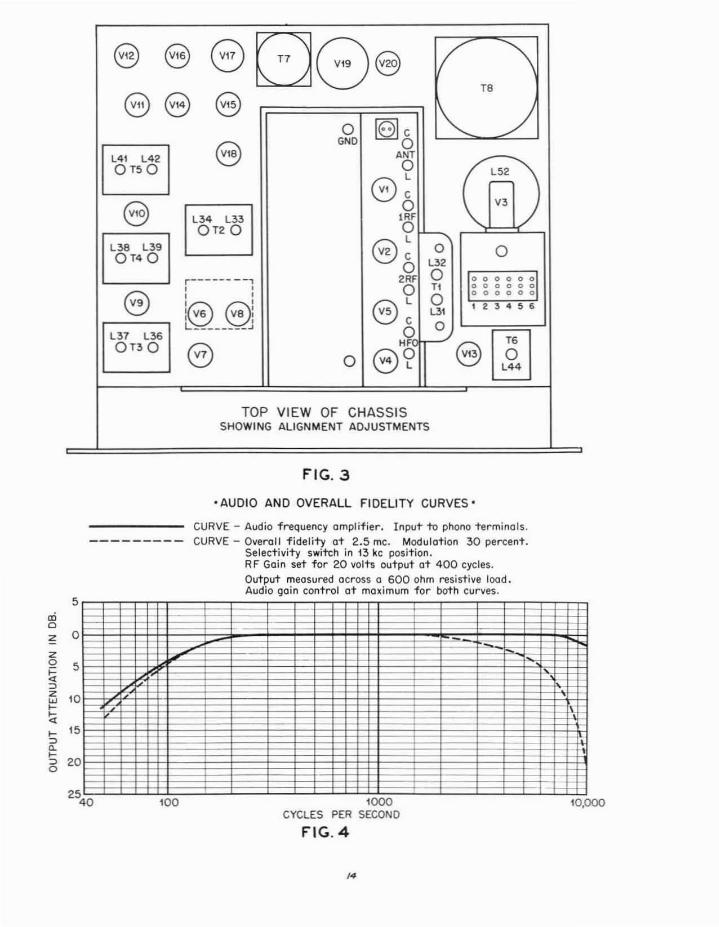
VIALIGNMENT
The alignment of a mndcrn communications re'ceiver requires precision instruments ilnd a thoroughkr)O\Vletl~c uf the circuits involved. This receiver, bemg .1 douhle super-hcterooyne. the <llignmcl'lt procc'dure is even more involved than is usual.
UIH.kr normal service the receiver will stay in aliJ!I1'ment for extremely long periods of time. Cf'lIlscqucntly
realiJ!nmcrH should not be attempted unless all otherpossible causes of a particular trouble h.\\'c been eliminated When It has hCt:11 ddcrmincd that any rc,d(l!nmenl should be ,ltu:mptcd, :1 g:rcat dc:d (If caution...hould be cl\crciscd in makin~ the adjustments. as an)'required readjustment should not entail mOre than aslight angu[M motion of lh..: aJjusting screw.
ALIGNMENT OF THE IF STAGES
The signal generator should be modulated :iO percent at 400 cycles. Turn the selectivity switch to the3 kc Dosition :lnd advance the RF Cain control tllmaxim'um. Sct the signal generator frequency to 455kc and adjus.t Its output until some deflection is not;.:don the Output meier. Refer to figure?> for the locationof the various alignment adjustments. Adjust L42.1.4 [, L:i9, L?>8. L?>6 and L32 for maximum output. rc'ducing the signal generator output and the RF Gaincontwl as required to prevent overload or excessiveoutput. Now lurn the selectivity SWitch to the narrow'est position, .2 kc. and adjust the sign,ll KencTrI!Or frcquency for the maximum nutpuL This establishes the
The low frequency IF should be aligned first, Therecommended method for aligning the low frequencyIF involves the use of 11 sweep frequency si~nal generator and ;U\ oscilloscope. Since thcSi: instruments arenot avaIlable at the average service station the alternate method using all amplitude modulated signal g.ma:\.lor and ;In output meter will be described first.The additional information required for the visualdlignmcllt nlcthod will be cov..:recl in a later paragraph.
Th..: si~nal gencr.llor should b..: coupled to the gridof the mixer tube V5 thmugh a capacitance of ap'proximately .01 mfd. A miniature tube adapter willbe required to make the mixer grid connection avail·.Ihle. Such an adapter is.mlll1\lfactured b}' the AkknManufacturing Co. An output meter should be connected across the output terminals of the receiver orthe speakl?r voice coil. The receiver controls shouldIIOW be Sd as follows:
COlilrolSelectivitySend~ Recci\''':CW~MoJ
PhasingAVC~ManAudIO CainRF GainHand SwitchDial
PosilionSec textRecckeModArrowManSet for approx. 20 voltsSec text1.35 - 3.45 me2.5 me
correct signal frequency by the 455 kc crystal for theIF amplifier and the frequcncy of the signal ~":llerator
should not be disturhed for the rcm.tinUo:t of the lowfrequency IF alignment, unless it should be to recheckthis establishment of crystal frequency to make sureth,lt the signal generlltor frequcn..:y h,ls not Jnftcddllnng the alignment. The sekl:tivity switch is nnwlurned to the?> kc position and L42, L41, U9. US.L?>6 and L:.2 :Ire ;Ig-al1l adJustct.l for maximum Output.Now turn the selectivity switch to th..: I.:' kc pos:tit1nand :ldjust U7 for maximum output. llcJor..: ch:lng'ing this sct-up the BFO should be turned on by throw·mg the CW-Mod switch to CW and checked for zerobeat with the BFa knob dial at its :i:ero read mg. Ifnecessary LH should be adjusted for :i:ero ompul. Thischeck and adjustment of the BFa should be done WIththe signal generator carrier unmodulatcd.
The procedure for the visual method of aligning thelow frequency IF should be the SJme ,u; the above ex..:ept thJt the adjustments arc made for hoth m;u;imum:Imphlud..: and coincidence of the oscilloscope images.The oscilloscope vcrtic,d input should be I:onllcctcdacross the dIOde detector load resistance, from thejunction of R64 <tnd R65 to ch~lssis.
The high frequency IF should be aligned next. Setthe band switl:h [0 th..: 7.4~ 1~.8 mc b<tnd. The sc'I.:::CtJvit}, switch should be in the:' kc position. Adju.stIhe si!!nal generator frequency to ;'.955 mc ami adjustUl, U:' ;1l1d U4 ffIT maximum output.
The ?> ..i mc I:rystal used III thlt s<;:cond ':(lllv.. rSIIHloscillator circuit is held to :\ wry dose frt.:qucilcy tolerance :lIld may be used <I.!' a frcqucney s[;:Uldard atmultiplc-s of :1.5 me from 10.5 Ttl..: upwards. III ordato do this. in \,iew of the .::umplete shlc1t.ling ag<tinstr,ldia.tioll from this os.6I1ator, it will be necessary !(\
t..:.mpor:trily connect a two foot length of Insul;Hedwire to the antenna terminal and dress the fre..: endof chis le:td around the tulle shield Oil th..: .~ ..s m\'CJscill,lwr tube V8. This t..:St kad should, of ..:our:...:.he rcmov..:d exr..:pt \vhd~' in us,' ,IS a fn:yu'·l1q·.;t.lndard.
ALIGNMENT OF THE RF AMPLIFIER & HF OSCILLATORTo ;uJcquately align the RF Amplifier and HF Os
cIllator an accur.ttdy calibrated slj.:nal generator lindan output meter arc required. The frequencies n:qui red arc shown in table :'t. The location 1)( the adJustments is showil in Figure ). The use of Table ~
and Figure:; should be made in following this put ufthe alignment which will llOW be described for uneircquenc)' band. The s.1mc procedure should then befollowed for the other frequency bands.
To align the .54-1.35 me band the sign.d generatoris coupled to the antenna input terminal through a100 ohm carbon resistor. The gcncr;llor should bemodulated :;0 percent at 400 cycles and the outp\llmeter cnnnected across the receiver Output terminals.The nX:l.'i\'cr controls should be set as follows;
ControlSelectivityS~nd·Reccive
CW-ModAVC-ManAudio GainRF GainBand SwitchLimiter
PositiOn:;kcRecei\,c.ModSec TextSet (or appro:.:. 20 voltsSec textset for band to be alignedoff
Set the re..:.:iva and signal generator dIals to .56 m.::.The RF Gam control should be set at maxmmrl"\ andIh;: AVe - Man .o;wHch sct Oll Ave. The HF Os,:. Ladjustmcm shown in Figure :;, should now t-l: set formaximum output. Then the Ant., 1st RF and 2nd RFI. adjustments should he .set for maximum output. Th~receiver and signal genc.r'ltor dIals are now set ttl I.:'me and the C adjustments, ~hown in Figure 3, shouldbe adjusted for maximum output in the same orJer,beginning with the Os.: C adjustment and then m,lk·ing: the C adjustments for the Am, 1st RF and 2ndRF. This proccdur\: should be ..:arcfully rcpe'ltcd un'til 110 inerc,,-sc in output can be r.::all:cd. The AVeMan switch should then be set II) Man and the sic-nalI-:enerator should he set for ,ipproximatc1y :; n~icro\'oIts. The Land C adjustments should now bechecked for maximum OutpUl, adjusting the RF Gaincontrol as found necessary to m,lintaill the output at;lpproximatc1y 20 vOllS.
Following the frcqUl::ncit:s, shown in Table 3, alignthe rcmainlllg banus using the same procedure .t$
above.
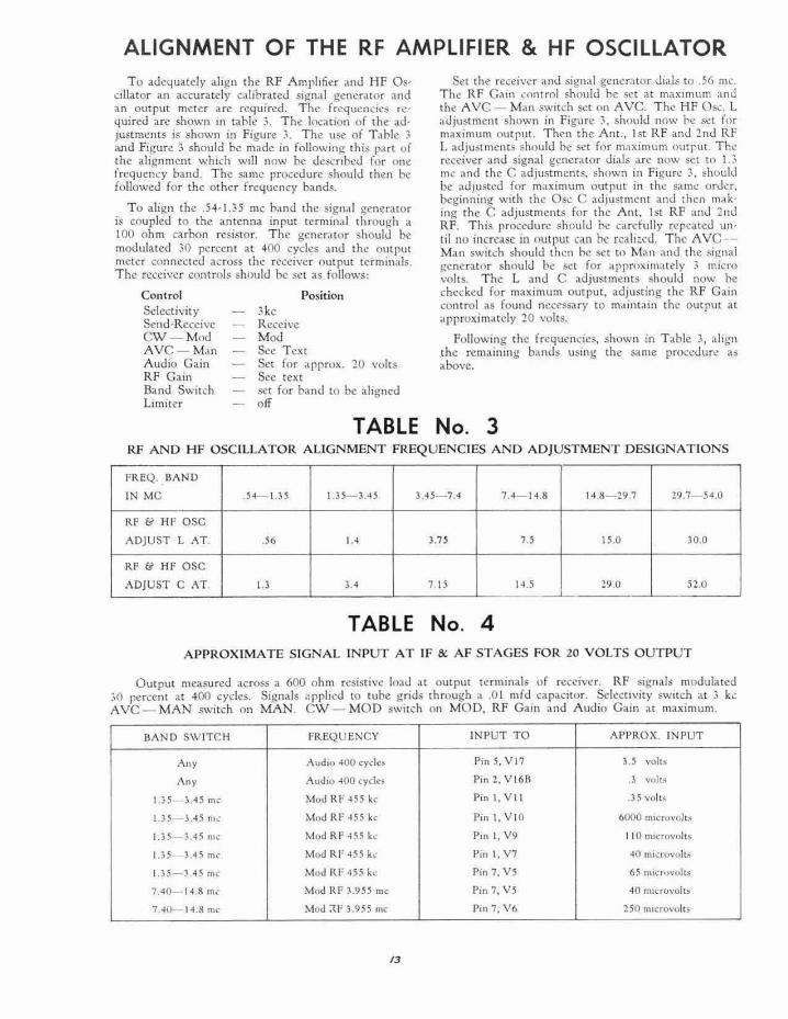
TABLE No. 3RF AND HF OSCILLATOR ALIGNMENT FREQUENC.IES AND ADJUSTMENT DESIGNATIONS
!'REQ. BAND
IN Me H-l.3~ t.H-3.4S 3.45-7.4 7.4-14.8 \4.8-297 29.7-54.0
Rf " HI' OSC
:\DJUST L ."T. .56 I.' 3.75 7.' 15.0 30.0
RF Ei HI' OSC
ADJUST C AT J.j ~.4 7.1S 14.5 29.U 52.0
TABLE No.4APPROXIMATE SIGNAL INPUT AT IF & AF STAGES FOR 20 VOLTS OUTPUT
Output measured across a 600 ohm resistive load at output terminals of rccciva. RF signals modulated30 percent at 400 cycles. Signals :lpphcd to tube ltrids through ,I .01 mfd capacitor. Selccllvity switch ;n 3 kcAVC-MAN .o;wit.::h On MAN. CW-MOD switch on MOD, RF Galli ;Ind Audio Gain at maximum.
BAND SWITCH FREQUENCY INPUT TO APPROX. INPUT
Any AudIO 400 cyel.:s 1'",5,V17 U ,"olts
Aoy i\udlO 400 eyell's Pin 2, VI6B ., ,"olt•
U5-).4~ me Mod RF 4H kc l)in I, VI t .35volt<
1.35 3.45 no.: l'o.·lod R!' 455 ke Pin l. VIO ClOOO 'meru\'olt.,
1.3 .•-345 Ill(' Mod Rf 455 ke Pm t. V? 110 nllcnwolts
1.35-3 4~ nit"" Mod RF 455 k.- Pm I, V7 40 lI"n"volts
l,l~-345 In,' Mud ItF 45~ k.. Pm 7. V5 65 Oller' "'olts
7.40~ 14 8 In". Mod R!' ~_955 me P'" 7. V5 40 Il"novolu
7.40-14.1I me Mod :~I' l.9~S me Pin 7, V6 2501llICrtwolts
13
§ 8 8 80@ 1/ '\T8
8 e e 1"'- /0 ~c
e OND 0L42 ANTL41
0OT50L ~GC
V3e 0L34 L33 'RFOT20 0
--."L38 L39 e~ 0 0OT40 L32
00i------ --, 2RF 000000, ,
0 Tl 000000
e , ,0
000 0 0 0
lee! @~ L3\ I 2 :5 4 5 6
L..: ________ J
00
L37 L36 rnOT30 6HF e 00 8? L44
TOP VIEW OF CHASSISSHOWING ALIGNMENT ADJUSTMENTS
FIG.3
'AUDIO AND OVERALL FIDELITY CURVES'
10,0001000CYCLES PER SECOND
FIG.4
CURVE - Audio frequency amplifier. Input to phono 'terminals.CURVE - Overall fidelity at 2.5 me. Modulation 30 percent.
Selectivity switch in 13 kc position.RF Gain set for 20 volts output at 400 cycles.Output measured across 0 600 ohm resistive lood.Audio goin control at maximum for bath curves.
100
,-
- ~
~ ,0
\
5
0
5
5
ozo 5~::>i1i \....\i....::>a.....::> 2o
<Xioz

• SELECTIVITY CURVESOverall at 2 Megacycles.
1
1510505KC OFF RESONANCE
FIG.5
10
NUMBERS DENOTE SELECTIVITY SWITCH POSITIONS1,2 AND 3 NON CRYSTAL - 4 15 AND 6 CRYSTAL
2 3 456 654 3 2
15
0
1\
0
i,
I
I
I
"' .... ~!.I
l.o::'
1a
100 1
10>-:::>"-zwuZ<IZ0(flW0::
(flW:;;>-
/5
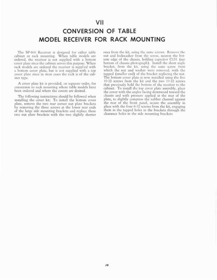
VIICONVERSION OF TABLE
MODEL RECEIVER FOR RACK MOUNTING
Tho.: SI'·60() RCCC1\"er 15 UC$l'i!I1Cd for either t<lbl..:cahinet or rack mounting. \Vhcll table modds arcordered. Ihe receiver is not supplied with a bottom.:o\'cr plate SIlH:C the cabinet SCfV':.s this purpOSl:. Wh.:nrack moods arc ord..red the rC';":lvcr IS suppl~cd WIth
a bottom cover pl.llC. but is not supplied WIth :1 topcover pl.IlC .;llllCe In milst elSC! the r:u:k is of the cabmet 1}'Po.:
A cover pl,tlC kit IS pro\'ldcd, Oil SoCpdr,lt..: order, forconversion to r,lck mountinj! where table models havebeen ordered and where the covers arc desired.
The following instructions should be followed whenlllslallin~ the -co\'er kit: To install the bottom co\'crp1:llc. rcmO\'e the twO rear corner nut plate bracketsby rcmovlIlg the Ihr.:c. screws at the lower rear endsof the large side mounting brackcts ;lnd r~place thesetWo nut plate buckets with Ihe two slIghtly shaner
oues from the kIt, USll1~ the $,\m,' 'erews. Remove th.::nut and lock.... asher from the !crcw, near.:st the bottom ec.Ig,; of the chassis. holdmg C,lpaCltur CIS I (~"
bottom of I:has,sls pholllgraph) Install Ihe short an!.:!ebracket, from Ihe kil, U~l1lg the ...1m,; s..:rew fromwhkh the nUl and washer wer..: rel1l()vec.I, with thet;tppcd (smaller end) of the bracket replal:lI1g Ihl: nutThe bottom CU\'U plate is now l1lstatled US1l1~ the fiv.-:10-32 screws from the kit ,lnd the two 10,32 screwsthat previollsly held the hottom of the receiver 10 thecabinet. To install the top cover plate assembly, pldeethe cover WIth the dn~1cs faclllg: dl)Wnward tow:trd thechassis anJ with pressure appheJ at the rear of theplate, to slightly compress the rubber chaonel againstthe rear of the front P,Ut.::!. s.::curc. the assembly inplace With the four 6-:;2 scr.:ws from the kit, eng<tgingthem in the tilpp.:J holes lI\ the brackets through theclearance holes III the sldc mountll1~ hrack':IS
'6
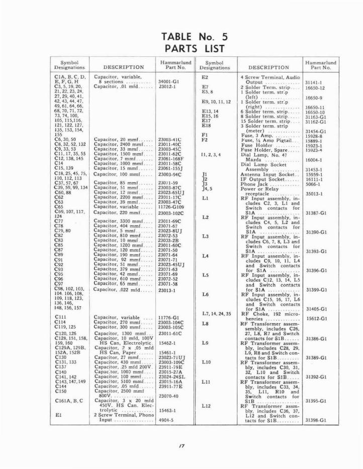
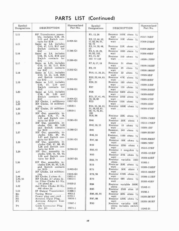
TABLE No. 5PARTS LIST
Symbol Hammarlund Symbol HammarlundDesignations DESCRIPTION Part No. Designations DESCRIPTION Part No.
CIA. B,C. D. CapOICilor, variable. £2 4 Screw Terminal. AudioE,F,G.H 8 sections 34001-0. Output _ 31141_1C3. $. 19.20. Capacitor, .01 mfd 23012_. £7 2 SoJdn Term. strip 16650-1221,22.23.24. ES.8 I Soldcr term. Slr:p21,29,40.41. (left) 16650-942,43.44, '!1. E9, 10. II, 12 I Solder' term.·~tr:p49,61. 64. 66. (riiht) .. 16650-1168.10.71. 72. E13.14 6 Solder term. strip .. 16650·\073.74. 100. E15,16 8 Solder term. strip .. JII6J·Ol105,115.116. £17 15 Solder term. strip 31162·Gl121. 122,127. £18 3 Solder term. strip135.153.154, (meter) ....... 31454-01IS' FI Fuse, 3 Am'p... .. 15928-8C6. 30. 50 Capacilor, 20 rnmf. .... 23003-41(,; F2 "'usc, !I.i AmI) Pit/:tail 158119.1C8. 32. 52. 132 Capacitor. 2400 mmf. 23011-40C Fuse Holder ... 15923-1C9. 33, 53 Capacitor, 33 mmf ...... 23003·45C Fuse Holder, Spare .. 15923·-'1Cll.17,35.55 Capacitor, 1500 mmf. 2301l·62C 11.2.3.4 Uial Lamp. No. -'17C12,138.145 Capacitor, 7 mmf . .... 23061.168F Muda
S~Ck;t16004·1
CI< Capacitor. 1000 mmf. 23011·58C Dial l.ampC15,1J9 Capacitor, 15 mmf ... 23061.155J Assembly 31453-1CI8.25.45.75. Capacitor. 100 mmf. .. 23003·94C JI AIlIenna Input Socket. 15959·1110. 1I2. 113 J2 IF Output Socket.. .. 16111-1C37.57.67 Capacitor. 85 mmf ... 2301\·59 J3 Phone Jack .. 5066-1C39, 59. 99.134 Capacitor. 51 mmf .. 23003·87C J4.5 Power or RdayC60.88 Capacitor. 12 mmf .. 23023·65UJ receptade 35013-1C62 Capacitor, 2200 mmf. 23011·17C LI RF Input asse~bly. in:C63 Capacitor. 39 mmf .... : ~ 23003.47C dudes C2. 3. L I andC" Capacitor, variable .... 11726·GI09 Switch contacts fo,C69.107.117. Cap.acitor.22O mmf.. 23003·102C SIA
~s~~~biy:.. 31387-GI
12' L2 RF Input in-
Icn Capacitor. 3300 mmf.... 23011-69C dudes C,. ,. L2 ,,'C78 Capacitor. 404 mmf... 23071_67 Switch contaca '0'C19.80 Capacitor• .5 mmf 23023·8UJ SIA 31 39O·G IC82 Capacitor. 810 mmf .. 23072·53 L3 RF Inp~; a~~~;"biy:·i~.C83 Capacitor. 10 mmf .. 230J3·28 dudcs C6, 7. S. L3 andC" Capacitor. 1200 mmf.. 2301I·6OC Switch contacts fo'C87 Capacitor. 120 mmL .. 23071·50 SIA
a~~e~bly. i~:31393·GIC89 Capacnor. 190 mmf. 23071·64 L' RF Input
C91 Capacitor, 92 mmf. .. .. 23011·71 dudes C9, 10. II . L,C92 Capacitor, 51 mm£.. 23023-45UJ '0' Switch contactsC93 Capacitor, 379 mmf .. 23071·63 fo, SIA
a~~~~bi;: 'i~:31396·GI
C" Capacitor. 42 mmf .. ... 23071_69 U RF InputCOO Capacitor. 610 rnmF .. 23072.52 dudes C12. 13. 1< . UC97 Capacitor, 65 mmf ... 23071-.58 '0' Switch COntaCISe98, 102. 103. Ca,Iacilor..022 mid .. " 23013-1 for SIA ... 31399-GI104. 106, 108, L' RF Illput assembly, in.109,118.123, dudes C15. 16. t7. L'136,146, '0' Switch contacts148,1.56,157 for SlA 31405·GI
L7, 14. 24, 35 RF Choke:' i92 micro-CIlI Capacitor. variable .. 11776·GI henries .. ...... . ... 15612·GICII4 Capacitor. 270 mmi. 23003.I04C La RF Transformer assem-C1I9,125 Capacitor. 300 mmf. .. :: 23003-105C sembly. includes C26,C120, 126 Capacitor. 1300 mmf . 23011-61C 27, L8, R7 and SwitchC128. 1.51, ISS. Capacitor. 10 mfd, IOOV contacts for SI8 ...•.. 31386-GI159.160 HS Can, Electrolytic 15462·1 L' RF Translormer assem·CI29A.I298. Capacitor. 2 • .0' mid bly. includes C2a. 29.152A,1528 HS Can. Paper 15-'161·1 L9. RS and S.....itch con-CI30
ICaj».citor. 27 mmf_ .. 23023·71UJ tacts for SI 8 .... _. 31389·GI
C131,13] Capacitor. 430 rnmf _. . 23003·109C 1I0 RF Translonner assem-CI3l Capacitor•.2.5 mfd 200V 23911·:i9E bly. includes C30. 31.CI40 CapaC:l0r. 100J mmf .. 23015·21A 32. LIO '0' SwitchC141,142 Capacitor, 100 mmf .. 23024-24SL contacts for SIB ..•.. 31392·GICI43.147.149 Capacilor. 5100 mmf 2301.5-16A LII RF Tran.sformer assem-CI44 Capacitor, .05 mfd .. 23911-77E bly, includes C33, 34.CI50 Capacitor. 2500 mmf ". LII. RIO '0'8OOV. .. 23070-40 Switch contacts fo'CI61A, B, C Capacitor. 3 • 20 mid SIB .. .. 31395·G I
4S0V. HS Can. Elec- L12 RF Tr'a'n"s1o'r~~~ . assm-trolytic 15463-1 bly. includes C36, 37.
£1 2 Screw Te~~j~~i:Ph~~o L12 '0' Switch con·Input ......... ...... 4904·5 tacts for SIB ... .... 31398·GI
17
PARTS LIST (Continued)Symbol
DesIgnations DESCRIPTIONHammarlund
Part No.Symbol
Dc:siRnalions DESCRIPTIONHammarlund
Part No.
15342-11
15342-21
19309·IBP
19309-45BF
19309·21881"
19396-1
19309-113BF
19310·179BF
19309-18181"
19309·79BF'
19309_287BF
19309-6981"
19309-5781"
19309-5381"
19309-97BF
19309_17081"
19309.19381"
19309-18981"
19309-981"
19309-898 I~
19309-3181"
19309-25981"
19309-2828 I"
19309_4981"
19317-7681"
19309-27881"
Resistor 51 ohms \Iiwall ..
Resistor 24 "hmswatt ..
Res:stor 22 ohmswatt
ReSistor 47K ohms \Iiwatt
Resistor 180 ohms Y;walt
Resistor 150 ohms Yiwatt
Resistor 6800 ohms Yiwatt., . , .... . . .. . ..
ResiStor 2200 ohms \Iiwatt.. . ...
Resisor 1500 ohms Viwatt., ., ...
Resistor lOOK ohms Yowatt., ..
Rui9tor 510K ohms l-Swatt .,
Resistor 10K ohms Y2wall
Resistor 33K ohms ~
watt .... ,. .. ',;Resistor 1000 ohms I/z
wattResistor 510 ohms
watt
Resistor 22K ohms Yiwatt.. 19309·1788F
Resinor 20K ohms Iwall
Resistor 10 ohms \Iiwatt ....
Resistor. 240 ohms Yiwatt .. 19309-201BF
Resistor, 1100 ohms Yiwatt
l<esistor 18K ohm;' V. 19309-208BFwatt
Resistor 2200 ohms Iwatt.. ., 19310-5781"
Resistor I megohm 'hwatt 19309_12181"
Resistor 27K ohms I/zwatt..... .. .. ".... 19309.83BF
Resistor variable 1000ohms. 15363-1
Resis:or 20K ohms Vzwatt ..
Resistor 56K ohms Iwatt... 19310.186BF
Resistor 470K ohms Vzwatt .....
Res:stor 680 ohms Vzwatt ..
Resistor variable SOOKohms ., .
Resistor 2500 ohm 10watts .
Resistor 82K ohms Y2watt
Resistor 120K ohms Vzwatt .
Resistor variable SOKohms includes switchSIO ..
Rl. 13.26
R2. 12. 44. 52.57.82.90.91.92.70R3. 14. 39, 48.53R4, 6. 16.29,30.83.102.R5.15.32103 10110
R7.8.17.18
R9.19
RIO. 11.20.21.
R22, 23. 64. 65,
"R24,25
R27
R28
R31. 37,41. 49.54.58.80R33
R59
R60.61
R63
R73
Ri8.98
R19
R84
Ras
R86, 89, 95
R87,88
R93
R46.94
R47.66
R69.74
R72
R34. 35. 38. 43,51.56,62,67.68.75.76,81.100R36.96
R40
R42, 50. 55
R<S31388-GI
31392·GI
31385·GI
31031_231488-14903-26143_116016-1
15987-1
16071_1
31397-GI
31394_GI
31391-GI
31404·GI15617·GI
15618·1
15619-1
31395-GI
31398·GI
31403-GI
1~16-GI
15611-115613-1
31030-2
31389-GI
31404-·GI
31386-GI
RF Transformer assembly, includes C38. 39,til and Switch con·tacts for SIB
Same as L8. includesC46. 47. LIS. R17 andSwitch contacts forSIC .. .. . ..... ..
Same: 35 L9. includesC48, 49. 1.16. RIB andSwitch contacts forSIC ""
Same as L10, includesC~O. 51. 52, 1.17, Rigand Switch contactsfor SIC ..
Same: as 1.11, includesC53, 54, 55, LI8, R20and Switch contac~s
for SiC .Same: as L12. includes
C56. 57. L19 andSwitch contacts lorSIC
Same: as 1.13, includese58. 59, L20 andSwitch conlatls forSIC
RF Choke, 1 ~fliil';~~;~RF Choke. 10 millihen.
ries .RF Choke, 25 millihen-
ries " .. ,.HI" Ost, assembly, in
cludes Ci6, 71, 78,L25 and Switch con·tacts for SID ..... "
HF Osc, assembly, in.c1udes C81, 82, L26and Switch contactSfor SID .. , .. , .
HI" Osc. assembly, indudes C83, 84. 85.L27 and Switch contacts for SID ...
HI" Osc. assembly, in·c1udes C8!i. 87, 88. 89,L28 and Switch contacts for SID ... , ...
HI" Osc, assembly includes C90, 91. 92. 93.L29 and Switch cont3ctS for SID
HI" Osc. assembly. indudes C94. 95. 96. L30.and Switch contactsfor SID .
RF Choke. 3,8 millihen-ries. .. ., ...
RF Choke. 2 ohms dc ..RF Choke, 2.7 ohms de.1st Filter Choke 8.5 H y,
170 ohms dc2nd Filter Choke 20 Hy,
440 ohms de .,I I" Output TransrormerTunin~ MeterPower plug and cordAntenna Input Plug ...Antenna Adapter Con·
nectorCable Connector Plug
(for J2)
L29
L2IL22
L23
L25
L20
L2S
L30
L19
P,
L27
L<7
L48L49. SOLSI
L53MIPIP2P3
L15
L16
L20
LI8
L13
L52
L11
"

PARTS LIST (Continued)
SymbolDC~lgnations DESCRIPTION
HammarlundPart No.
SymbolDesignations DESCIHI-'TlON
HammarlundPart No,
16092-5
15989-5
l1227·GJ
31227·G2
l1227-G5l1463-1l12l9-1
l1U7·G1
l120S-131434·GIl1<462·GIl1215-GIJ1227-GI
31125_1l1126_1
15989-J16100-1
31473-spec.
ll130-lll~71-1
11806-211806-l11806-429619·2l1275·GI
Tube soc:ket, miniature,ceramic, less center
shield ....Tube socket, miniature,
ceramic. with centershield . .. ,
Tube socket. "Noval"Crystal socket. c:eramic.
for c:rystals VI to Y6Crystal. order special.
spedfy signal fre.quency ...
Crystal. l.5mcCrystal. 455kc .Wrench. SCI screw No.6Wrench, set screw No.8Wrench. set screw No. 10Snap Bulton Plug .Shaft Coupling, rigId .Shaft Coupling, Rexible,
soh.. .,.. 415·G3Shalt Coupling. R~~ible.
stiff.. . ... 41$·G2Spring. l'elainer for RF
coil assemblies" liOOl-1Spring, retainer lor RF
coil' _ ". .. 310G4-1Spring, grounding for IF
transformer shields ' JI023·1Spring. com'ersion
switch ...Spring. indicator slideSpdn!:". band change
detent ., ".Knob, frequency controlKnob, tunin!: lock .Knob & Skin (large) ..Knob & Dial (RF Gain)Knob & Dial
(Audio Gain)Knob & Dial
(Crystal Phasing)Knob & Dial
(Beat Freq. Osc.)Knob & Dial
(Selectivity). .. ,Chart, frequency controlSpring, anti-backlash ,
XS
XI8X21
YI.2.J,4,5.6
X4
VIV8Miscellaneous
lll02·GI
l1106-GI
31086-231029-2
15989.4
16082-1
l1114·GI
l1102-GI
l1116-GI
3118l-GI
15880-1
15852·1
15856-115864-115866-115867·1
31234·GI15879·131469-1
19309-133BF19310·211BF
15342·4
Resistor 3.3 megohmsYo: waH .
Resistor 360 ohms I wattResistor variable 25K
ohms .Swill;:". base and spring
assemblyCrystal selector switch.Crystal switch .Switch, conversion
switching .Selectivity switch, 3 sec-
lion ,_ .Toggle Switch SPST ..Toggle Swhch DPST ..To~"lc Switch DPDT..SWlIch "ON-OFF" pan
of R93 .. . .....Switch, DPDT, spring
return..... . .Mixer plate coil assem
bly. includes C67. 69.70. L31. 32. R31 ...
IF Transformer assem·bly. includes C97, 98,99. L33. 34. R35 .
Crystal Filter assembly,includes CI07, 110,111.112. 113, II~. U6. 37.R41, Y8 .,. . ..
I F Transformer, includesCI17, 118. 119. 120,L38, 39. 40. R49, ... ,
Same as T4, includesC123. 124. 125, 126.L41. 42, 43, R54 ."
Beat Frequency Osc:.assy.. includes C130,13!. 132, 133. 134, L44,'IS. 46, R76, 77" ..
Transformer, AudioOutput
Transformer. Power
Tube soc:ket, mmiature.
Tube socket, octal
T2
TS
T1
T8
Xl,2,6.7.8.9.10, II, 12. 13.14,15.18.20Xl17.19
T3
T.
SSA. D.C
56.9S1S8SIO
SII
TI
SIA. B, C. 0
S2S3S'
R97
R99RIOt
/9

FIG.6REAR VIEW OF RECEIVER
20
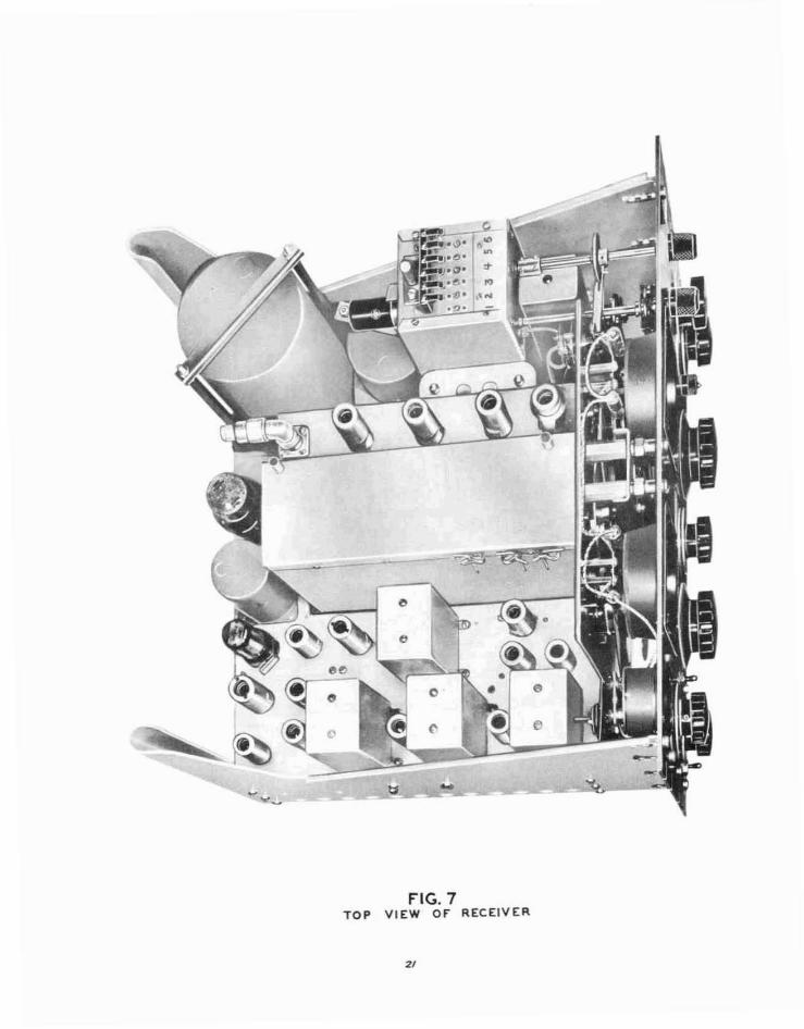
FIG. 7TOP VIEW OF RECEIVER
21
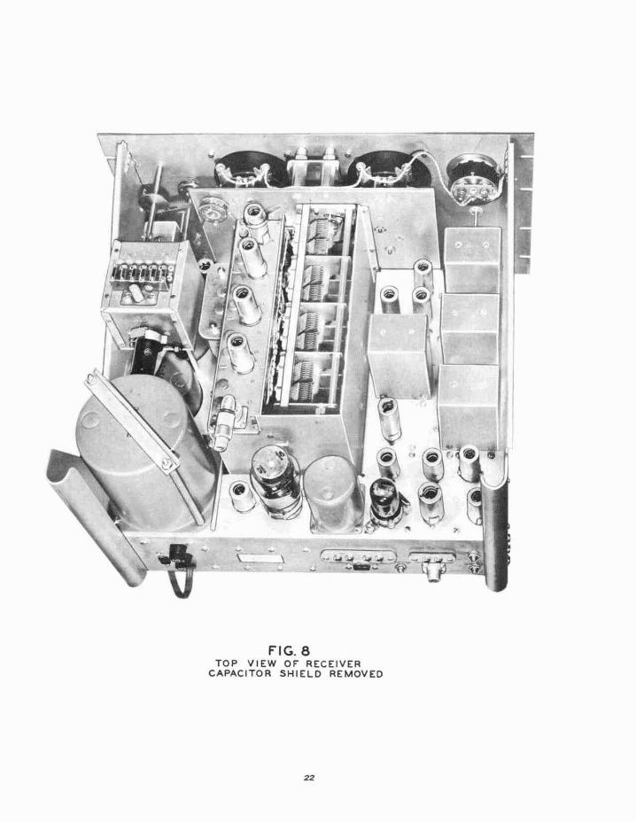
FIG.8TOP VIEW OF RECEIVER
CAPACITOR SHIELD REMOVED
22

...
o·-<u<
FIG.9BOTTOM VIEW OF" RECEIVER SP-600-JX
23
e.::=f,j--R"ROO
'".-"1--- gS\c,'"",.","Cl"9e,
C ...
'"FlIOI."Re,.,.C,m
;C147
-::::~~~ll~n
t:::"$-t!==:R"R102
R"C\4$RIOO.,.
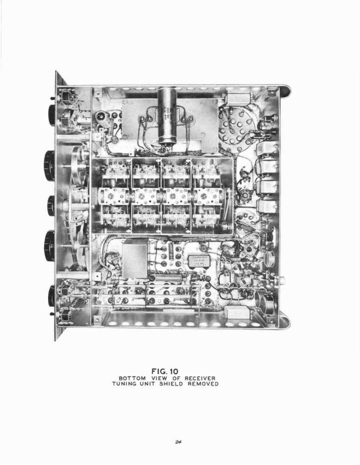
FIG.l0BOTTOM VIEW OF RECEIVER
TUNING UNIT SHIELD REMOVED
II SINGLE CO!'iV(IISlONI .S<l·T4 tile
I
...( •..-_.
N
"•
'"V7GSA
,.------IIIIIIII'ntl2q:~f"sa::JN-- ---
1"·~<IM, CIO! ...
" ,'-' f
II.
//
/
n
" "w ffi~s.
RELAY
n
C7'
'" ®5
l----*-h~
.1~~"I·I.,.,.I,I
)'1I II II II II II II 1/
/rfI II II ,
: II I
L30 ~ I,)'-----.,jIH"!!:---'"1.1-- •
1- *,---0-,..,IC95 t
t ••C66 us ~ ~
.------iIHiiTf~ , C81
,
FREQ.CONTROL
2ND RFV2
68A6
'25 ". , CO,
s"rf ®- r1'CO, m
R~~ ;;llC41 • C1!~
~+ C4~ ,
-I"i~;r. RI~ I, uF t
•
,
•,,II
TIlt ' K';=" '- ~ ,,;~ f--11rt iCIC~ " CIO L __"o',.JL-,-'-C/j'" L_C'7"C/+-,-c--'/~CIHi
__ L __ ...L...____ .£ J. _ J_../ I
TUNING I,I,,I-,I,II
lSI RFVI
68A6
,
'"•
JI
•
:!tcr-,---=-,------,--,~
ro~
2Htl MIXER
2>ll> IF
YOO6BA6
.12
"6BA6
1ST IF
'",,
:' ~R"1: .-7 o~1..,-- ..... __ 0_°_
SELECTIVITY SW.
ss.
GATE
"GBAG,
',nv ~.~'J: ~ GO
CONV£IlSION.<
CI RCUIT DIAGRAM or RECEIVER
25-26
"
<,
REGULATED 150 v: __
'"~CJ6IC
S8 Ave
I-':~
.~_0Cco'.~co
"f ••, <,10 V.
I ••, <III
,•<
CI38
2ND IF DRIVER
"0 VII
6BA6 6BA6
", c
i'-~;----~-- --,
~, ,, ,, "I::in: ~ '+-=:_{,r--=c'
,1-=,. ,119 :;:1 R50
2 :-6r , •,"
JII 1 l <l:,
0 II I... s:Jl 1 ~T,= 0"'- , ~ 1lI1!';! a:"'- U-, ;; • , : :~N:~, ,. • , l ~ U1.I C;
'",± •:~1 '"
1_ •'N • I -
~~:OI N I• 10 = •• • I . ,,
N, , ,---1,.J , I 0
L ___ ---- - --'NON XTAL
CI39
;;;•
V,.2/lD DET a Ave.
GAL5
,., ~ *" R67~ ~C!41
~ : $C142
VI5
LIMITER 6OUTPUT
METER.6ALS
" 12AU7 VI6B1ST AUDIO,
0' - t
~VI'
OUTPUTGVGGT
'r./ r--.I •• I, .-
••
,v.IolnEIl '"Ae ~r-r--'=
IF
57
, ", I ~I •
:::~I
~:f:I ,I ,I •
-~ I
'" J-
• " I T7 J.-,•
'"• r0 1; ie ~0 §, •• ' ' •, L.- • , •• '" I r,
,, , ~
PHONES,
J' ~
C!.E...l1 OFF :~-+ ' IolDD-CW
VI2BUffER6BA6,
• "' '" ''0 RIO!• R.f.• METER
10 V. " I OUTPUT
• k©1 "LEVEL
" ,w,• ~,• 'l.F..A.F, LEVEL A.F.
S8 AV~r:--
, lolA"'.0
'EO 150 v._
- XTAL
/' '- VI8~' Lt.m' \1 OA 2
~V~-VDLTAGe RCG.
V '0, RECTIfiER6ALS
FIG. '1:UlT DIAGRAM OF RECEIVER
25-25

,"
'eo
MAIN WIRING CABLE...,....-...; CIQ2: iGR~C~'~£O~- ,F.i'~.J"-'-GR
l I 2:3'f
h S'
NOTE. SWITCHON TUNING UNI~S MOUNTEDBY BANDswrTCH OPERATED
2-3 CLOSED 8ELOW'-2 CLOSED ABOVE 74 Me14 Me
.:-I~4;----~~:~I~3~_·elJ.!A"C",,--_----~·i'l~-,[---
,,
,.LU -RED
'@
o
B A K-WHI
co,
, -,"
BLACK
WH-GREEN
WHITE-BlA K
27-'
N-
59
••
••
!:""
EI C
WHlTE-Q, ACK
,.CI06
~":"'~ WHIT'
> '0O~
;~vi56' T200 ,'z~i
i6~ ... 2" .II: .i:fIE91 _
"
27-28
FIGURE NUMBER 12 CHASSISM- RE,(C; EEJlIVo'EE,!R,--,,-==_j;CC!'0,!!N~N!!:E~CC!T~I02!N~D~1A",G",R.:.:A~_

'S3 ,..OTE: THIS SWITCHCLOSED ON POSITIONS1-6 OF 52
TO CiD ON FREOllEtlCYCONTROL UNIT
, THESE NUMBERS "IE FOR REHII[NCE a'lLVTtlEY DO ,..OT ilPPEUI ON TERMINAL STRIP
lui
~ANT-:::Q..INPUT
RED-GUEN
BlACl\
"o
Y[LlOW-BlACIl
"OTt HUMBERS ON
~ ~c!:F ~:~T(G~·:·:~~s1RE, ON SCI1[MATIC 01,1,-
1:::\. . ::::/2:0S~~i~HAND SWITCHASS[IllILlU
TO
--I,"::IJ(j)~V~I'4f"-'~
>l@
FIGURE 13
CONNECTION DIAGRAM
TUNING UNIT
•U,
SLACK
'-24
III'II'
REO-GREEH
GREEN'WHITETO CHASSIS
[11 T£Fl)r,IIIUll£14 TERIIIINH T
8lUf:-lllAClotTO CI1ASSIS12. TERMINAL".
Ili
000
L-:a-:-4
,~
GIiASSIS
"
:ot~
TO CIGl RE
'"' THESE NUMBERS ARE FOR REFERENCE ONLY.THEY 00 NOT APPEAR ON TERMINAL STRIP,
, CIG!
"j,
•
0
I
'"•
•
N
~
EB
"
C65
TO SWITCH S3SEE TUNING UNIT Ol06.GR06.M
FIGURE /4CON N ECTION DIAGRAM
FREQUENCY CONTROL UNIT
C60
3/

Notes
1ST RF
"6BA6
2ND RF
"6BA6
.
25-26
'"2,,0 OET 6 AVeGAL5
'"LIMITER aQUTPUl
METERGALS
, '

$9
<u<
\
YEL W
EI8
$~l
~ YE ,SlK
L5>
',11
\ J2~r_~__~-_~~h'i=-__--jO:69
ft::;::> EI c
, II
U• '""
8LACK-WHI E
BLACK-WHITEB ACK-WHlT
REO-BlA K
WHITE
• I
~"
WHITE-BLACK
'C,),12 ~ 11
~==
BLACK. -
I
RB4 '/2,
NOTE; $W1TCH 1$ MOUNTEDON TUNING UNIT OPERATEDElY BANOSWITCH2-3 CLOSED ElELOW 1.'1lo1C1- 2 CLOSED ABOVE 7.4 Me
C02
l'..
r-__C"C':.:IN WIRING CABLE
2
,
• I
~
B A K -WHIT
L52 'i!fa.
(~
9 01
"",I 0
[51 ""
I 2 , ,')
~,\
.. < •.It ~)o u~<-
R90 +,.oJ' f' "'••'~
e , ~•~,• ,
WHITE-BLACK
FIGURE NUMBER 12CONNECTION DIAGRAM- RECEIVER CHASSIS
THESE NUMBERS ARE FOR REFERENCEONLY THEY DO NOT APPEAR ONTERMINAL STRIP.