modeling and simulation of closed loop controlled zvs non-isolated
TRANSCRIPT
Abstract- This paper deals with the design, analysis and simulation
of ZVS controlled non-isolated converter. The prominence of this topology is to diminish the conduction losses and complexity of the circuit. The non-isolated converter used as DC-DC converter is suitable for low and medium power application. The aspire of this work is to build up the blocks of Simulink ZVS controlled non-isolated DC to DC converter. The 48V DC voltage is stepped down to 12V DC. The switches in this proposed topology is operated under ZVS condition to decrease the switching loss. The Non-isolated DC-DC ZVS Converter is modeled using Simulink and the simulation results are presented. Keywords- Closed Loop Control, Non-isolated Converter and ZVS.
I. INTRODUCTION NCLUSION of power electronic converter is getting increased because of increased applications such as Industrial
equipment, Household appliances, Motor drives, Tractions, Switched power supplies etc.High power density is an everlasting topic on power electronics. The effective way to improve power density is to increase switching frequency. In order to rise the switching frequency, the switching loss should be reduced at first. The fast switching power semiconductor devices, such as MOSFET or IGBT are used as they have less switching losses, small in size, lower in cost and as higher efficiency. Moreover, due to the limited energy storage capability of batteries, the efficiency requirement for DC/DC converter in UPS systems [1] will be high. Thus, the study on the soft-switching push-pull converter has become more and more essential. DC-DC converter with soft-switching operation with high power and isolated bi-directional operation is given in [2].
Advanced applications in power electronics such as renewable energy systems, high-frequency systems require incredible increase or decrease in voltage ratio is given in [3]. This absurd change in voltage ratio will make the duty ratio to exceedingly high or low. The operation using small duty cycle in buck converter cases influences the steady state and transient state performance.
Mrs. S. Devikala is PhD Student, Sathyabama University, India. Email: [email protected].
Dr.P.NirmalKumar is working as an Assistant Professor in Anna University, India.
This small duty cycle reduces the efficiency of power as well as characteristics of transients with the small pulse width [4].Simulation and experimental verifications of soft switched DC to DC converter is given by Lui [5].
ZV/ZC resonant push-pull converter is given by Mori [6]. The autotransformer is replaced by the tapped inductor. Furthermore, copper loss is less because of one winding in autotransformer than that of an isolation-type transformer [7]. Though, there are some disadvantage like higher voltage stress and increased EMI due to leakage inductance and parasitic capacitance .These problems avert the use of tapped inductor for the best solution for intense variation of ratio applications. The conventional critical conduction mode buck converter that has a ZVS operation extended by the tapped-inductor turn ratios [8]. High efficiency DC to DC converter with high voltage gain and reduced switching stress is given by Wai [9]. DC to DC converter is energy storing interfacing in fuel cell hybrid vehicles is given by Vacca [10]. High efficiency parallel port regulator for wide range input DC to DC converter is given by Wang [11].A bidirectional DC to DC converter for low power application is given by Jain [12]. To overcome the drawbacks this topology has been proposed which reduces the switching losses, complexity of the circuit, minimize EMI and increase efficiency. The circuit model for closed loop control of ZVS resonant converter is developed using simulation The above literature does not deal with Simulink modeling of closed loop controlled DC to DC converter. This work proposes a model for closed loop DC to DC converter. In this paper, zero-voltage switching buck converter with the tapped-inductor is proposed.
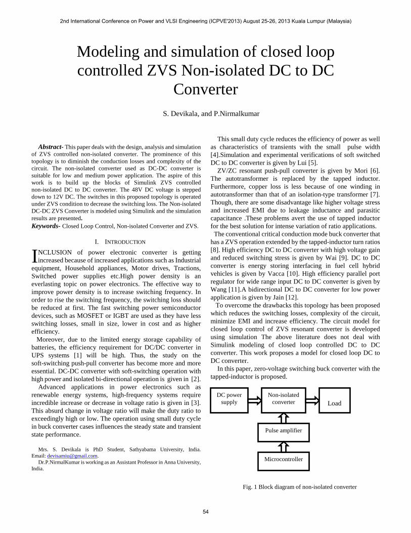
Fig. 1 Block diagram of non-isolated converter
Modeling and simulation of closed loop controlled ZVS Non-isolated DC to DC
Converter S. Devikala, and P.Nirmalkumar
I
DC power supply
Non-isolated converter
Load
Pulse amplifier
Microcontroller
2nd International Conference on Power and VLSI Engineering (ICPVE'2013) August 25-26, 2013 Kuala Lumpur (Malaysia)
54

The converter is fed from pulse amplifier which has been generated by microcontroller. The basic block diagram of non-isolated converter is shown in fig: 1 .In this 48V DC is stepped down to 12V DC voltage and is fed to load. The switching pulse hence soft-switching technique is incorporated in order to minimize these problems.
The paper is organized as follows. In section II the basics of non-isolated converter are presented. In section III the circuit description and operating principle of proposed topology is presented. In section IV simulation results of the converter are presented. Finally, section V gives the conclusion of the proposed work
II. NON-ISOLATED BUCK CONVERTER The DC load is supplied by buck converter. The buck converter is shown in Fig:2a
Fig: 2a DC-DC Buck converter
The assumption is as follows: The switches are assumed to be ideal. Steady state operation is used for converter. In order to maintain the output voltage constant, the
capacitor value used should be large. Inductor current operates in continuous conduction
mode. Ideal buck converter is designed as shown in Fig: 2b
Fig: 2b Buck converter with MOSFET and DIODE
Mode:1 S1 is ON The switch S1 is switched ON is shown in Fig:2b (i).As S1 is ON, the diode gets reverse biased therefore the input voltage appears across LC filter. Thus the inductor current start building up and transfers the energy to the capacitor and builds the output voltage. Let S1 be ON for a time period DTs and OFF for the period (1-D) Ts=D’Ts, where D is the duty ratio.
By KVL,
0=++− oLg VVV [1]
ogL VVV −= 2]\
Fig: 2b (i) Switch S1 is ON
Mode: 2 S1 is OFF The S1 is switched OFF as shown in Fig:2b (ii). As S1 is OFF, the inductor current will not suddenly drops to zero but will not change instantaneously. Hence the energy stored in the inductor keeps the voltage across the capacitor constant. Thus forward biases the diode and forms the closed path for the discharge of the inductor current. By KVL
0=+ oL VV [3]
oL VV −= [4]
Fig: 2b (ii) Switch S1 is OFF
Fig: 2c (i) Capacitor current
2nd International Conference on Power and VLSI Engineering (ICPVE'2013) August 25-26, 2013 Kuala Lumpur (Malaysia)
55
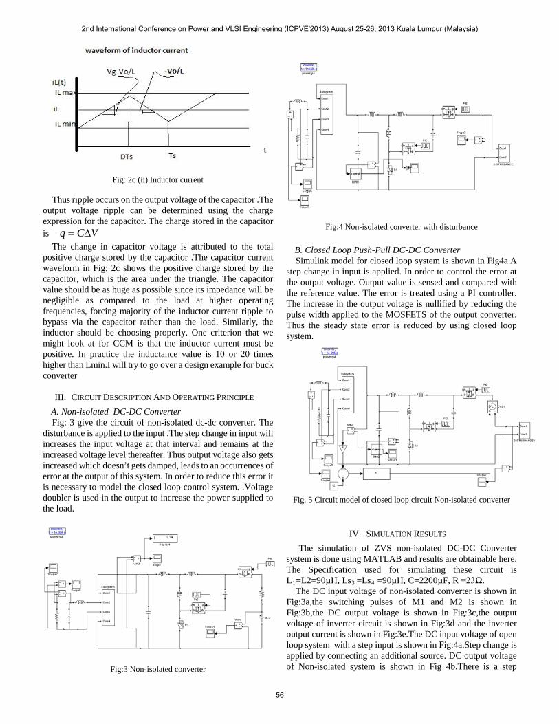
Fig: 2c (ii) Inductor current Thus ripple occurs on the output voltage of the capacitor .The output voltage ripple can be determined using the charge expression for the capacitor. The charge stored in the capacitor is VCq ∆= The change in capacitor voltage is attributed to the total positive charge stored by the capacitor .The capacitor current waveform in Fig: 2c shows the positive charge stored by the capacitor, which is the area under the triangle. The capacitor value should be as huge as possible since its impedance will be negligible as compared to the load at higher operating frequencies, forcing majority of the inductor current ripple to bypass via the capacitor rather than the load. Similarly, the inductor should be choosing properly. One criterion that we might look at for CCM is that the inductor current must be positive. In practice the inductance value is 10 or 20 times higher than Lmin.I will try to go over a design example for buck converter
III. CIRCUIT DESCRIPTION AND OPERATING PRINCIPLE A. Non-isolated DC-DC Converter
Fig: 3 give the circuit of non-isolated dc-dc converter. The disturbance is applied to the input .The step change in input will increases the input voltage at that interval and remains at the increased voltage level thereafter. Thus output voltage also gets increased which doesn’t gets damped, leads to an occurrences of error at the output of this system. In order to reduce this error it is necessary to model the closed loop control system. .Voltage doubler is used in the output to increase the power supplied to the load.
Fig:3 Non-isolated converter
Fig:4 Non-isolated converter with disturbance
B. Closed Loop Push-Pull DC-DC Converter Simulink model for closed loop system is shown in Fig4a.A step change in input is applied. In order to control the error at the output voltage. Output value is sensed and compared with the reference value. The error is treated using a PI controller. The increase in the output voltage is nullified by reducing the pulse width applied to the MOSFETS of the output converter. Thus the steady state error is reduced by using closed loop system.
Fig. 5 Circuit model of closed loop circuit Non-isolated converter
IV. SIMULATION RESULTS The simulation of ZVS non-isolated DC-DC Converter
system is done using MATLAB and results are obtainable here. The Specification used for simulating these circuit is L1=L2=90µH, Ls3 =Ls4 =90µH, C=2200µF, R =23Ω. The DC input voltage of non-isolated converter is shown in Fig:3a,the switching pulses of M1 and M2 is shown in Fig:3b,the DC output voltage is shown in Fig:3c,the output voltage of inverter circuit is shown in Fig:3d and the inverter output current is shown in Fig:3e.The DC input voltage of open loop system with a step input is shown in Fig:4a.Step change is applied by connecting an additional source. DC output voltage of Non-isolated system is shown in Fig 4b.There is a step
2nd International Conference on Power and VLSI Engineering (ICPVE'2013) August 25-26, 2013 Kuala Lumpur (Malaysia)
56

change in the output voltage, this is due to the step change in the input voltage. The inverter output voltage is shown in Fig: 4c and current through the load is shown in Fig: 4d. In closed loop system a step change in input is applied shown in Fig: 5a. Output is sensed and it is compared with the reference value. The error is processed using a PI controller. A controlled converter is suggested at the output. The increase in the output voltage is nullified by reducing the pulse width applied to the MOSFETS of the output converter. The output voltage of the proposed converter system is shown in Fig: 5b. It can be seen that the error is reduced by using closed loop system. The inverter output voltage and output current is shown in Fig: 5c and Fig: 5d.
2nd International Conference on Power and VLSI Engineering (ICPVE'2013) August 25-26, 2013 Kuala Lumpur (Malaysia)
57
V. CONCLUSION Non-isolated DC/DC Converter is simulated using
MATLAB. The error occurred in the output voltage is shown in the simulated output waveform. Then the closed loop system is modeled and simulated successfully and their results are presented in this paper. The result shows that the error produced has been attenuated by the use of PI controller. The converter presents a range of avenues for new research. Non-isolated Converter can be used to increase switching speed, reduce hardware, reduce switching losses and EMI. The extent of this work is modeling and simulation of ZVS DC-DC non-isolated converter. The hardware will be implemented in future. The simulation results are in line with the prediction.
REFERENCES [1] Kwok Kai & Yim-shu Lee, “An Integrated Fly back converter for DC
UPS”, IEEE Trans. Power Electronics, Vol II, No. 2 March 1996. [2] K.Wang,C.Y.Lin,L.Zhu,D.QU,F.C.Lee &J.Lai, “Bi-directional DC to
DC converter for fuel cell systems”, in Conf.Rec 1998 IEEE workshop on Power Electronics In Transportation, pp 47-51.
[3] Qun Zhao, Fengfeng Tao, Yongxuan Hu, Lee, F.C., “Active-clamp DC/DC converters using magnetic switches,” IEEE Applied Power Electronics Conference and Exposition, Page(s): 946 –952, vol.2, 2001.
[4] J Kingston, R Morrison, M. G. Egan, G Hallissey, “Application of a passive loss-less snubber to a tapped inductor buck dc/dc converter,” IEE Power Electronics Machines and Drives 2002, 445-450
[5] Lui Li, Fang Z.Peng & J.Lawler, “Modeling, Simulation & experimental Verification of Soft-Switched bi-directional DC-DC Converters”, IEEE APEC proceedings 2001, pp 736-742.
[6] I.Boonyaroonate & S.Mori, “A New ZVCS Resonant Push-pull DC/DC Converter Topology”, IEEE APEC’ 2002.
[7] Kaiwei Yao, Yuancheng Ren, Jia Wei, Ming Xu and Fred Lee, “A family of Buck type DC-DC Converters with Autotransformers,” IEEE APEC 2003, 114-120
[8] J.H. Park, B.H. Cho, “The zero voltage switching (ZVS) critical conduction mode (CRM) buck converter with tapped-inductor,” Applied Power Electronics Conf., Vol. 2, pp. 1077 –1081, Feb. 2003.
[9] R.J.Wai, C.Lin & Y.Chang, “High Efficiency DC/DC Converter with high voltage gain and reduced switch stress”. IEEE Transaction Power Electronics, Vol 54, No.1, Feb 2007, pp 354-364.
[10] Marchesoni M, Vacca.C. “New DC-DC Converter for Energy Storage Interfacing in Fuel Cell Hybrid Electric Vehicles”, Power Electronics, IEEE Transactions on, Vol 22, Issue 1, Jan 2007, pp 301-308.
[11] Wang X.C, Tian F, Batarseh I, “ High Efficiency parallel post Regulator for wide Range input DC-DC Converter”, Power Electronics,IEEE Transactions 0n 2008, pp 852-858.
[12] M.Jain, M.Daniele & P.K.Jain, A bi-directional dc-dc converter topology for low power application”, IEEE Transactions on Power Electronics, Vol .15, No.4, pp595-606, July 2010.
S.Devikala received her BE degree in Electrical and Electronics Engineering from Bharath Institute Of Technologt, Madras University, Chennai in the year 1999.She has done her M.E. degree in Power Electronics and Industrial Drives from Sathyabama University, Chennai in the year 2003. She has 13 years of teaching experience.Currently she is a research scholar at
Sathyabama University Her areas of research interest are ZVS push-pull DC to DC Converter. Mail id:[email protected],Ph:9789047410 Dr.P.Nirmal Kumar received his B.E degree from in Electronics and Communication Engineering from Madras University in the year 1998. He has done his M.E. Barathiyar University in the year 2001 and PhD from Anna University in the year 2008 currently he is working as an Assistant Professor in Anna University. His areas of research interest DC to DC Converter. Mail id:[email protected]; Phone: 9444141048
2nd International Conference on Power and VLSI Engineering (ICPVE'2013) August 25-26, 2013 Kuala Lumpur (Malaysia)
58